1
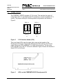
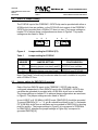
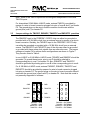
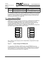
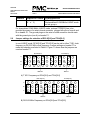
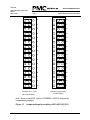
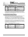
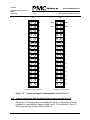
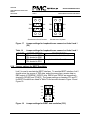
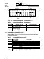
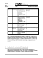
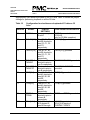
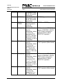
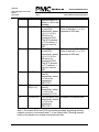
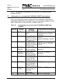
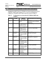
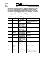
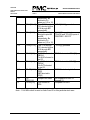
PM2352 FREEDM -32P672 RELEASED DEVELOPMENT KIT BOARD USER MANUAL PMC-2001840 ISSUE 1 P11 RCLK[31:16] P13 TCLK[15:0] P14 TCLK[31:16] P7 RCL52[2:0] P7 TCL52[2:0] P15 TD RD[15:2] P10 TD RD[31:16] P2 TD RD[1:0] DEVELOPMENT KIT BOARD USER MANUAL C15 shorted to pins B0 through B15 respectively Pins C16 through C31 shorted to pins B16 through B31 respectively Pins C0 through C15 shorted to pins B0 through B15 respectively Pins C16 through C31 shorted to pins B16 through B31 respectively No shorting jumper placed on this header No shorting jumper placed on this header Pins A2 through A15 shorted to pins B2 through B15 respectively Pins A16 through A31 shorted to pins B16 through B31 respectively TD0 shorted to RD0, TD1 shorted to RD1 RCLK[31:16] grounded TCLK[15:0] grounded TCLK[31:16] grounded Loopback on links 2 through 15 Loopback on links 16 through 31 Loopback on links 0 and 1 Note 1: 4.096 MHz oscillator should be placed in socket OSC 2. Note 2: If all the link-groups are not configured for unchannelized 2.048 Mbit/s HMVIP mode, unused RMVCK and TMVCK should be grounded. No shorting jumpers should be used over unused RD and TD. For example, if link-group 0 alone is configured for unchannelized 2.048 Mbit/s H-MVIP mode, 4.096 MHz clock should be provided to RMVCK[0] only. Hence, on header P5, pin B0 should be shorted to A0, whereas pins B1, B2 and B3 should be shorted to pins C1, C2 and C3 respectively (i.e. RMVCK[3:1] grounded). Also, pins corresponding to TD[31:8] and RD[31:8] are not shorted to each other. PROPRIETARY AND CONFIDENTIAL TO PMC-SIERRA, INC., AND FOR ITS CUSTOMERS’ INTERNAL USE 39