1
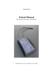
QDS
QwikRadio™ Development System
User’s Guide
Covers the follow parts:
DS-QDS-315
DS-QDS-418
DS-QDS-433
DS-QDS-915
RF Laboratories, Inc.
QwikRadio™ Development System User’s Guide
Table of Contents
QwikRadio™ Development System Limitations
QwikRadio™ Development System Warranty
1. QwikRadio™ Development System Introduction
1.1 General Description
1.2 Intended User
2. Getting Started
2.1 QDS diagram
2.2 Quickstart instructions
3. Assembly and QDS Overview
3.1 Assembly of Development System
3.2 Jumpers and DIP Settings
3.3 Power Supply and Regulation
3.4 Microcontroller (MCU) Section
3.5 Antenna Options and Interfaces
3.6 RS-232 Interface
3.7 Breadboard Area
3.8 Receiver Section
3.9 Transmitter Section
2
4. Operation Instructions and GuidelinesSample Firmware
4.1 Theory of Operation
4.2 I/O Interface
4.3 LED, Piezo and Button Functions
4.4 Microcontroller Protocol
4.5 RS232 Interface and Windows Software
5. Developing Applications with Micrel’s QwikRadio™ IC’s
5.1 A QwikRadio™ Overview
5.2 Reference Oscillator and External Timing Element
5.3 Slicing Level and the CTH Capacitor
5.4 AGC Function and the AGC Capacitor
5.5 Antenna Design Considerations
5.6 Bandwidth and Data Rate
5.7 Noise Management
6. Low-power Radios and Regulatory Compliance
6.1 Electromagnetic Compliance
6.2 A Regulatory Overview
7. FAQ’s
8. Sample Firmware
9. QDS Diagram
10. Data Sheets and Application Notes
3
QwikRadio™ Development System Limitations
The QwikRadio™ Development System (“QDS”) is intended for use by engineers for the purpose of
evaluating the feasibility of implementing the QwikRadio™ series of Micrel’s RF IC’s in various wireless applications. The user’s environment must be limited to use of the development system within an
environment which provides for adequate isolation of RF emissions which might be caused by operation
of the QDS. In field testing, the device must not be operated in a residential area or any area where radio
devices might be subject to harmful electrical interference. The development system has not been certified for use by the FCC in accord with Part 15, ETSI I-ETS 300 220 or I-ETS 300 220-1 regulations, or
other known standards of operation governing radio emissions. Distribution and sale of the QDS is
intended solely for use in future development of devices which may be subject to FCC regulation, or
other authorities governing radio emission. QDS may not be resold by users for any purpose. Accordingly, operation of the QDS in the development of future devices is deemed within the discretion of the
user and the user shall have all responsibility for any compliance with any FCC regulation or other
authority governing radio emissions of such development or use, including without limitation reducing
electrical interference to legally acceptable levels. All products developed by user must be approved by
the FCC or other authority governing radio emission prior to marketing or sale of such products and user
bears all responsibility for obtaining the FCC’s prior approval, or approval as needed from any other
authority governing radio emissions.
QDS is an experimental device, and RF Laboratories, Inc. (“RFL”) makes no representation with respect
to the adequacy of the QDS in developing low-power wireless data communications applications or
systems, nor for the adequacy of such design or result. RFL does not and cannot warrant that the functioning of the QDS will be uninterrupted or error-free.
The QDS and products based on the technology in the QDS operate on shared radio channels. Radio
interference can occur in any place at any time, and thus the communications link may not be absolutely
reliable. Products using the QwikRadio™ technology must be designed so that a loss of communications
due to radio interference or otherwise will not endanger either people or property and will not cause the
loss of valuable data. RFL assumes no liability for the performance of products which are designed or
created using the QDS. RFL’s products are not suitable for use in life-support applications, biological
hazard applications, nuclear control applications, or radioactive areas.
4
QwikRadio™ Development System Warranty
RF Laboratories, Inc. (“RFL”) warrants solely to the purchaser that the hardware components of the
QwikRadio™ Development System (QDS) will be free from defects in materials and workmanship
under normal use for a period of 90 days from the date of shipment by RFL. This limited warranty does
not extend to any components or circuits which have been subjected to modification, misuse, neglect,
accident, or improper installation or application. RFL’s entire liability and the purchaser’s sole and
exclusive remedy for the breach of this Limited Hardware Warranty shall be, at RFL’s option, when
accompanied by a valid receipt, either (i) repair or replacement of the defective components or (ii) upon
return of the defective QDS, refund of the purchase price paid for the QDS. EXCEPT FOR THE LIMITED HARDWARE WARRANTY SET FORTH ABOVE, RFL AND ITS LICENSORS PROVIDE
THE HARDWARE ON AN “AS IS” BASIS, AND WITHOUT WARRANTY OF ANY KIND EITHER EXPRESS, IMPLIED OR STATUTORY, INCLUDING BUT NOT LIMITED TO THE IMPLIED WARRANTIES OF NONINFRINGEMENT, MERCHANTABILITY OR FITNESS FOR A
PARTICULAR PURPOSE. Some states do not allow the exclusion of implied warranties, so the above
exclusion may not apply to you. This warranty gives you specific legal rights and you may also have
other rights which vary from state to state.
Limitation of liability. IN NO EVENT SHALL RFL OR ITS SUPPLIERS BE LIABLE FOR ANY
DAMAGES (WHETHER SPECIAL, INCIDENTAL, CONSEQUENTIAL OR OTHERWISE) IN
EXCESS OF THE PRICE ACTUALLY PAID BY YOU TO RFL FOR THE QDS, REGARDLESS OF
UNDER WHAT LEGAL THEORY, TORT, OR CONTRACT SUCH DAMAGES MAY BE ALLEGED (INCLUDING, WITHOUT LIMITATION, ANY CLAIMS, DAMAGES, OR LIABILITIES
FOR LOSS OF BUSINESS PROFITS, BUSINESS INTERRUPTION, LOSS OF BUSINESS INFORMATION, OR FOR INJURY TO PERSON OR PROPERTY) ARISING OUT OF THE USE OR INABILITY TO USE THE QDS, EVEN IF RFL HAS BEEN ADVISED OF THE POSSIBILITY OF
SUCH DAMAGES. BECAUSE SOME STATES DO NOT ALLOW THE EXCLUSION OR LIMITATION OF LIABILITY FOR CONSEQUENTIAL OR INCIDENTAL DAMAGES, THE ABOVE
LIMITATION MAY NOT APPLY TO YOU.
5
1. QwikRadio™ Development System Introduction
1.1 General Description
The QwikRadio™ Development System comprises the hardware, firmware and software resources
commonly used by wireless designers in the design and development of wireless applications. The
QwikRadio™ Development System (QDS) offers a comprehensive test suite that allows the developer/
designer to vary a number of electrical firmware, software and antenna parameters to facilitate the
optimal architecture and topology for the given application being developed.
1.2 Intended User
The QwikRadio™ Development System (“QDS”) is intended for use solely by engineers for the purpose
of evaluating the feasibility of implementing the QwikRadio™ series of Micrel’s RF IC’s in various
wireless applications. The user’s evaluation must be limited to use of the development system within a
environment which provides for adequate isolation of RF emissions which might be caused by operation
of the QDS. In field testing, the device must not be operated in a residential area or any area where radio
devices might be subject to harmful electrical interference. This Kit has not been certified for use by the
FCC in accord with Part 15 ETSI I-ETS 300 220 or I-ETS 300 220-1 regulations or other known standards of operation governing radio emissions.
6
7
Transmitter
Antenna Jack
Momentary
Buttons
MCU DIP
Switches
RS232 Port
Breadboard Area Receiver Test Points Receiver Section
Relay Terminals 9V Battery Holder Compartment
(opposite side)
FIGURE 1
Jumper Bus MCU LEDs
Piezo Element
Transmitter Section
Microprocessor
(MCU)
2.2 Getting Started
Required Equipment:
QDS (QwikRadio™ Development System)
- Two QDS development boards (Figure 1)
- Two antennas
- Two 9 volt batteries
- QDS user’s manual
*
QDS Windows software
*
Two computers each with one available 9 pin, serial communication port
and Windows 95 or later installed.
*
Two serial cables - male to female, DB9
Note 1: For RS-232 Windows-based Software Testing Only
Setup:
1. Select a location that lends itself to wireless testing, i.e., line-of-sight with as
few metal objects and RF pathway obstructions as practical.
2. Ensure that jumper and dipswitch settings match that required for desired test.
Units are shipped with the radios interfaced to microcontroller.
3. Install 9 volt battery in holder underneath each development board.
4. Install two monopole antennas per unit into PCB mounted jacks indicated by
“Receiver Antenna Jack” and “Transmitter Antenna Jack” in Figure 1.
5. Turn power switch to the “ON” position, and you are ready to test.
8
3 Assembly and QDS Overview
3.1 Assembly of Development System
The QwikRadio™ Development System comes assembled in a default configuration for immediate
evaluation except for battery and antenna installations.
3.2 Jumpers and DIP Settings
The QDS units are shipped with the following default jumper settings:
(“ON” MEANS THAT JUMPER IS INSERTED, “OFF” MEANS THAT IT IS NOT)
JUMPER BUS:
RECEIVER CONFIGURATION SETTINGS:
RXDATA -> MCU (ON)
RXDATA -> 232 (OFF)
RXDATA -> BB (OFF)
RXWUP -> MCU (ON)
RXWUP -> BB (OFF)
RXSDN -> MCU (ON)
RXSDN -> BB (OFF)
RELAY -> MCU (ON)
RELAY -> MCU (OFF)
FETSW -> MCU (ON)
FETSW -> BB (OFF)
TXDATA ->MCU (ON)
TXDATA ->232 (OFF)
TXDATA ->BB (OFF)
+5V -> RXPWR (ON)
+5V -> TXPWR (ON)
+5V -> 232PWR (OFF)
SEL0 (ON)
SWEN (ON)
SEL1 (ON)
SDN (ON)
*
The settings may be modified after the demands of the respective application.
3.3 Power Supply and Regulation
The QDS units are power by a 9 volt alkaline cell and regulated with a industry standard 7805 voltage
regulator. The board’s VCC/VDD is therefore 5 volts.
9
3.4 Microcontroller (MCU) Section
All QDS’s are supplied with an on-board, 4 MHz, flash-based, microcontroller (MCU). It can be reprogrammed up to 10,000 times with an inexpensive programmer. The MCU comes pre-programmed with
sample code which allows the user to transmit and receive simple asyncronous protocol with its corresponding QDS unit. The sample code can be modified in an ASCII editor and reprogrammed according
to the requirements of the user’s application. The MCU is connected to the receiver’s data output, wakeup and power down features, as well as, the transmitter’s data input, two LEDs, a piezo element and one
relay.
The MCU comes pre-programmed with embedded firmware and software which supports simple,
asyncronous communication between both QDS development boards. The sample code includes a basic
method for preemption detection, LED and relay activation as well as a warbling beep routine to drive
the on-board piezo element.
3.5 Antenna Options and Interfaces
The QwikRadio™’s antenna input can be matched to a number of external antennas by using the “L”
inductor network provided on the development unit.
The QDS allows for two antenna polarizations and several different antenna types such as monopole
whip, helical, helically loaded whips and others. There are two antenna feed ports: horizontal SMA and
direct PCB mount via the on-board jack. The units a shipped with two monopole whip antennas which
are inserted directly into the transmit and receive antenna ports (Figure 1)
3.6 RS-232 Interface
The Windows-based software supplied with the QDS package permits the users to communicate PC to
PC where both QDS units are connected via their RS232 port and the associated jumpers are appropriately placed.
3.7 Breadboard Area
The development board offers a prototype area with several 0.100” spaced vias. There are also VCC
and GND rails provided at the top and bottom of this section.
3.8 Receiver Section
The receiver section is the core of the development system and the primary purpose for its use. The
receiver area includes one QwikRadio™ RFIC which comes with a factory preset frequency.
10
The reference frequency can also be generated by an alternate crystal oscillator in the receiver section
(Figure 1). The user must populate and calibrate the alternate oscillator as it does not come pre-installed
from the factory. All QwikRadio™ series chips allow the user to select between different baud rates and
either a scanning or fixed local oscillator (LO). The development board allows the user to quickly and
easily reconfigure these settings by the placement or removal of shorting jumpers. In addition, the units
provide two different automatic gain control (AGC) configurable settings: positive and ground bias.
Several different data slicer reference configurations are also possible: integrator capacitor, voltage
reference, divider and variable among others.
3.9 Transmitter Section
The development system board includes a transmitter which can be used to test the receiver portion of
the system if other external transmitters or signal generators are not available. The on-board
transmitter’s frequency, modulation and baud rate are all set to match the default configuration of the
receiver as shipped from the factory.
11
4 Operation Instructions and Guidelinesample Firmware
4.1 Theory of Operation
The QDS system employs one receiver and one transmitter per unit. Transmission and reception of
wireless data is controlled in one of three ways: by microprocessor, RS232 (PC) or external hardware
mounted in the prototyping area.
The development boards ship with microprocessor control as their default setting. After applying
power, the asyncronous preemption can the initiated by the depression of SW2 (the yellow momentary
button). The data packet is a simple three byte word preceded by a two byte preamble to place the
comparator threshold of the QwikRadio™ IC in at optimal bias for reception of the first byte of data.
As the QwikRadio™ receiver IC demodulates the received data from the transmitter, the IC’s data
output is sent to either the MCU, RS232 or breadboard for processing. If the MCU is interfaced to the
RFIC, the sample firmware will acknowledge a valid data packet by responding with a beep, blink an
LED once and finally toggle the on-board relay between states. If both QDS boards are jumpered to the
RS232 interface and connected to a PC with the QDS development software via a serial cable, the
RFIC’s data output will be shown in the software “received data” display screen.
The units come with two monopole antennas which employ the ground plane of the QDS board itself as
a reference. The socket the antennas use will also accept other antennas with diameters between 0.048"0.064". Located on the edge of the receiver side of the units (Figure 1, “Receiver Antenna Jack”) is an
SMA edge connector footprint intended for future installation of an SMA connector in the event the user
desires to supply a signal to the QwikRadio™ receiver from another signal source.
4.2 I/O Interface
The QDS boards are provided with one RS232 port, one relay output and one SMA edge connector
footprint.
4.3 LED, Piezo and Button Functions
The development system is shipped with the microprocessor jumpered such that a depression the yellow
button on the left side of the QDS will prompt the transmission of one data packet. The LED will light
also to indicate that a transmission did indeed occur. The piezo element in turn is prompted to warble as
an indication of a valid reception of one data packet.
4.4 Microcontroller Protocol
The microcontroller is preprogrammed with a simple asynchronous protocol intended to serve as a
starting point for those unfamiliar with wireless data transmission. It consists of a three-byte word
preceded by a two-byte preamble to place the comparator threshold of the QwikRadio™ IC in an optimal bias for reception of the first byte of data. The protocol in hexadecimal is as follows: FF, 00, F5,
AA,AA.
12
4.5 RS232 Interface and Windows Software
Installation:
Insert QDS CD into PC and navigate to “QDS Windows Software (Installation Files)\setup.exe”.
Follow all prompts, and repeat process for other PC to be used in test.
The RS232 port is located to the rear of the both units (Figure 1, “RS232 Port”). After installing the
QDS development software and determining which serial communication port is free for use, connect a
nine-pin serial cable between the QDS RS232 port and the PC’s serial communication port.
To open the QDS software, go to the Windows start menu, and after going into programs, scroll down
to QwikRadio™ Development System. Before starting your testing, it is necessary to designate a communications port from the scroll-down menu labelled “Comm Port” to the right of the “File” menu. Next a
baud rate must be assigned in the next menu tab to the right. The baud rates for both sides of the QDS
system must match each other in order for the units to communicate. The last menu bar is to execute a
clear screen function which clears the receive data screen of all of its contents.
The preamble section in the lower left hand corner of the QDS software window contains two userdefinable bytes that can be modified to experiment with comparator bias levels which are necessary to
optimize for best reception of the first data byte of the transmitted data packet.
The three header bytes can be used for redundancy or as address bytes. They will, along with the preamble bytes, be transmitted with every packet. It is necessary that the header bytes match each other in
both QDS software windows.
The software also facilitates a checksum feature which is activated by selection of the “Checksum”
radial box. The final feature of the program is an auto-transmit switch which causes the last entered data
packet to be re-transmitted continuously.
After all of the above settings have been determined, set and are matching in both QDS software windows, testing may begin by simply typing any text into the lower window label “Transmit Data.” Thereafter, each depression of the “Send” button will cause the current data in the “Transmit Data” window to
be transmitted once.
If user desired to experiment with different baud rates, care must be taken that the QwikRadio™ receiver
IC bandwidth settings match the data rates used in the QDS software.
13
5 Developing Applications with Micrel’s QwikRadio™ IC’s
5.1 A QwikRadio™ Overview
The QwikRadio™ series RF IC’s are single chip OOK (ON-OFF Keyed) receiver IC for remote wireless
applications, employing Micrel’s QwikRadio™ technology. All RF and IF tuning is accomplished
automatically within the IC, which eliminates manual tuning and reduces production costs. Receiver
functions are completely integrated. The result is a highly reliable yet extremely low cost solution for
high volume wireless applications. Because the QwikRadio™ IC is a true single-chip radio receiver, it is
extremely easy to apply, minimizing design and production costs, and improving time to market.
The QwikRadio™ IC provides two fundamental modes of operation, FIXED and SWP. In FIXED mode,
the device functions like a conventional superheterodyne receiver, with an (internal) local oscillator
fixed at a single frequency based on an external reference crystal or clock. As with any conventional
superheterodyne receiver, the transmit frequency must be accurately controlled, generally with a crystal
or SAW (Surface Acoustic Wave) resonator. In SWP mode, the QwikRadio™ IC sweeps the (internal)
local oscillator at rates greater than the baseband data rate. This effectively “broadens” the RF bandwidth of the receiver to a value equivalent to conventional super-regenerative receivers. Thus the
QwikRadio™ IC can operate with less expensive LC transmitters without additional components or
tuning, even though the receiver topology is still superheterodyne. In this mode the reference crystal can
be replaced with a less expensive ± 0.5% ceramic resonator.
All post-detection (demodulator) data filtering is provided on the QwikRadio™ IC, so no external filters
need to be designed. Any one of four filter bandwidths may be selected externally by the user. Bandwidths range in binary steps, from 0.625kHz to 5kHz (SWP mode) or 1.25kHz to 10kHz (FIXED mode).
The user only needs to program the appropriate filter selection based on data rate and code modulation
format.
5.2 Reference Oscillator and External Timing Element
All timing and tuning operations on the QwikRadio™ IC are derived from the reference oscillator
function. This function is a singe-pin Colpitts-type oscillator. The user may handle this pin in one of
three possible ways:
•Connect a ceramic resonator
•Connect a crystal
•Drive this pin with an external timing signal
The third approach is attractive for further lowering system cost if an accurate reference signal exists
elsewhere in the system (e.g. a reference clock from a crystal or ceramic resonator-based microprocessor), and flexibility exists in the choice of system transmit frequency. The user should AC couple this
signal into the REFOSC pin, and resistively divide (or otherwise limit) the signal to approximately
0.5Vpp. A sinusoid is preferred, and sharp transitions on this signal should be avoided to the extent
possible.
14
5.3 Slicing Level and the CTH Capacitor
Extraction of the DC value of the demodulated signal for purposes of logic-level data slicing is accomplished by external capacitor C TH and the on-chip switched-cap “resistor ” R SC. The effective resistance of R SC varies in the same way as the demodulator filter bandwidth, in four binary steps, from
approximately 1600k to 200k. Once the filter bandwidth is selected, this “resistance” is determined; then
the value of capacitor C TH is easily calculated, once the slicing-level time constant is determined.
Values vary somewhat with decoder type, but typical slicing- level time constants range 5ms to 50ms.
Optimization of the C TH value will be required to maximize range.
5.4 AGC Function and the AGC Capacitor
The signal path features automatic gain control (AGC) to increase input dynamic range. An external
capacitor, C AGC , must be applied to set the AGC attack and decay time-constants. With the addition
of only a capacitor, the ratio of decay-to-attack time-constant is fixed at 10:1 (i.e. the attack time constant is 1/10th the decay time constant), and this ratio cannot be changed by the user. However, the
attack time constant is selectable by the user through the value of capacitor C AGC . By adding resistance from the C AGC pin to VDDBB or VSSBB in parallel with the C AGC capacitor, the ratio of
decay-to-attack time-constant may be varied.
5.5 Antenna Design Considerations
Three types of antennas are normally associated with QwikRadio™ applications, (1) quarter-wave
monopole, (2) helical (coil), and (3) pcb loop. Of these antenna types, the quarter-wave monopole is
preferred, giving the best range performance. Typical SR and SH receivers employing quarter-wave
monopole antennas generally provide about 100 meters open field range. The QwikRadio™ IC is
designed to be connected to a quarter-wave monopole antenna at its input ANT pin, with no further
coupling network, and provide this similar range. Of course, the monopole can be a free-standing
“wire,” or a metal trace built directly into the pcb. The antenna need not be a quarter-wavelength long,
but shorter lengths will reduce range. Although the other two antenna types, helical and pcb loop, are
less efficient antennas than the monopole, they provide cost and/or ergonomic advantages. The pcb loop
antenna is a very inexpensive structure to produce, being built into the pcb. The only requirement is that
there be enough “room ” on the pcb to build a sufficiently effective antenna. This antenna has the
further advantage that it can be hidden from the end- user. The primary disadvantage is that this is
usually the least efficient of the three antenna types being discussed, with a typical range of 30 meters.
Loop antennas are more commonly found in transmitters than receivers. Where the antenna must be
hidden, but still be rather efficient, a good choice is the helical antenna. The structure is simply a “coil ”
of wire, inexpensive, and easy to fabricate. Typical range for this type of antenna is 60 meters. (Both
helical and pcb loop antennas are commonly found in transmitter designs, which usually requires a small
unit with the antenna hidden from the user.) Another aspect of antenna selection, aside from its effectiveness at “picking-up ” signal from the “ether,” is its directionality. Every type of antenna has its own
signature of energy distribution in the 3-dimensional space that surrounds it. This signature is generally
composed of “peaks” and “nulls”; if the transmit antenna “peak” is pointed at the receiving antenna’s
“peak,” then range is maximized. However, optimizing this for a particular application or installation is
generally not practical. All one can do in these cases is choose the antenna that meets the other constraints, like cost and form-factor, then test to determine if the system provides adequate range in all the
required directions and orientations. Unfortunately, much of this work is empirical.
15
Antenna types are described above without any special coupling circuits required. However, Micrel
does recommend some sort of DC path be provided from the ANT pin to VSSRF. This could be provided by an LC filter attached from the ANT pin to VSSRF, or simply a resistor. The ANT input is
internally AC-coupled, so no external biasing is required. The input circuit impedance is very high (i.e.
a FET gate), shunted by approximately 2pF of parasitic capacitance, giving an input AC-impedance of
about 200 Ω at 400MHz. Specialized 50 Ω antennas may also be connected directly to the MICRF001.
The antenna should be connected as closely as possible to the IC pin, minimizing parasitic inductance
between the antenna pad and the pin. (Use a >25mil trace,<200mil long, if possible). The antenna can
be located away from the pin of the device, but this requires using a transmission line from the antenna
to the IC input pin and an impedance matching coupling circuit. Micrel does not recommend such an
approach for users who lack the necessary RF expertise and test equipment to design transmission line
matching networks.
Suitable antennas are crucial to the success the application. Here are several key points to consider in
designing antennas for your application:
Where possible, the antenna should be placed on the outside of the product. Also, try to place the antenna on the top of the product. If the product is “body worn”, try to get the antenna away for the body
as far as practical.
Regulatory agencies prefer antennas that are permanently fixed to the product. Antennas can be supplied
with a cable, provided a non-standard connector is used to discourage antenna substitution (these connectors are often referred to as “Part 15” connectors).
An antenna can not be placed inside a metal case, as the case will shield it. Also, some plastics (and
coatings) significantly attenuate RF signals and these materials should not be used for product cases, if
the antenna is going to be inside the case. The antenna designs used in the kit are included in the Drawings section of the manual. Many other antenna designs are possible, but efficient antenna development
requires access to antenna test equipment such as a vector network analyzer, calibrated test antenna,
antenna range, etc. Unless you have access to this type of equipment, the use of an antenna consultant is
recommended. A patch or slot antenna can be used in some applications where an external antenna
would be subject to damage. These types of antennas usually have to be designed on a case-by-case
basis.
5.6 Bandwidth and Data Rate
The inputs SWEN, SEL0 and SEL1 control the operating mode and selectable features of the IC. These
inputs are CMOS compatible, and are pulled-up on the IC. The inputs SEL0 and SEL1 control the
Demodulator filter bandwidth in four binary steps (625Hz—5000Hz in SWP, 1250Hz—10000Hz in
FIXED mode), and the user must select the bandwidth appropriate to his needs.
16
5.7 Noise Management
Noise sources are found in all places and at all times. So the real question regarding noise generation and
management is not IF but: how much, what frequency and at what amplitude. Radios which operate
under FCC “Part 15” guidelines are subject to noise like any other receiver. Some noise sources commonly encountered by wireless developers are microprocessors, motors or fans, high frequency logic
circuits among others. When there exist sufficient speed regarding the rise time and fall time of microprocessor clocks, harmonics can be found around critical frequencies of the receiver. If the option exists,
the designer should choose a microprocessor that has the slowest rise and fall time possible for the given
application to avoid problematic harmonics relative to the receiver. Swithing power supplies, brush-type
motors and other radio unfriendly devices should be avoided around the receive circuitry. Adequate
bypass capacitors, chokes, series resistors and shielding can be helpful in managing such problems.
17
6 Low-power Radios and Regulatory Compliance
6.1 Electromagnetic Compliance
All low-power radio utilizing a frequency 9 Khz or about is subject to electromagnetic compliance and
conformance. Often these devices use less than 1 mW or 0 dBm of power, operate shorter distances (1 to
1000 feet) and are simple in design.These devices are unlicensed meaning that they may be used without
the end user having to apply for any other type of FCC authorization. In that the frequencies these
devices use are shared by millions, one has to take occupied bandwidth inference into account when
determining if the desired application is suitable for this regulatory area.
Normally part 15 or low-power radios are used for short-range low-cost applications where human life
or safety are not considerations. Among some of these are remote controls for automotive and home
alarms, garage door openers and simple contact closers amoung others. Data and telemetry is also
another area where Part 15 devices are employed. QDS is intended to support the design of these types
of low-power wireless applications. Most low-power wireless systems operate with few interference
problems. However, these systems operate on shared radio channels, so interference can occur at any
place and at any time.
6.2 A Regulatory Overview for The United States
Although the QwikRadio series RFIC’s normally do not exceed the FCC regulations for unintentional
radiation, the wireless developer should be aware of the requirements for the transmitter being used.
Non-licensed transmitters operate on a variety of frequencies. They must share these frequencies with
licensed transmitters and are prohibited from causing interference to licensed transmitters.
The Federal Communications Commission (FCC) has rules to limit the potential for harmful
interference to licensed transmitters by low-power, non-licensed transmitters. In its regulations, the
FCC takes into account that different types of products that incorporate low-power transmitters have
different potentials for causing harmful interference. As a result, the FCC’s regulations are most
restrictive on products that are most likely to cause harmful interference, and less restrictive on those
that are least likely to cause interference.
This overview is intended to provide a general understanding of the FCC’s regulations and policies
applying to products using low-power transmitters. It reflects the current text and interpretations of
the FCC’s regulations. More detailed information is contained in the regulations themselves, which
can be found in Part 15 of Title 47 of the Code of Federal Regulations.
Manufacturers and parties selling low-power, non-licensed transmitters, or products containing
low-power, non-licensed transmitters, are strongly encouraged to review the FCC’s regulations closely.
Recognizing that new uses of low-power transmitters often generate questions that are not directly
addressed in the regulations, we welcome inquiries or requests for specific interpretations.
Occasionally, the FCC proposes changes to its regulations, generally to address industry concerns
and/or as new uses of low-power transmission equipment appear.
18
The terms “low-power transmitter,” “low-power, non-licensed transmitter,” and “Part 15 transmitter” all
refer to the same thing: a low-power, non-licensed transmitter that complies with the regulations in Part
15 of the FCC rules. Part 15 transmitters use very little power, most of them less than a milliwatt. They
are “non-licensed” because their operators are not required to obtain a license from the FCC to use them.
Although an operator does not have to obtain a license to use a Part 15 transmitter, the transmitter itself
is required to have an FCC authorization before it can be legally marketed in the United States. This
authorization requirement helps ensure that Part 15 transmitters comply with the Commission’s technical standards and, thus, are capable of being operated with little potential for causing interference to
authorized radio communications.
If a Part 15 transmitter does cause interference to authorized radio communications, even if the transmitter complies with all of the technical standards and equipment authorization requirements in the FCC
rules, then its operator will be required to cease operation, at least until the interference problem is
corrected.
Part 15 transmitters receive no regulatory protection from interference.
Changing the antenna on a transmitter can significantly increase, or decrease, the strength of the signal
that is ultimately transmitted. Except for cable locating equipment, the standards in Part 15 are not based
solely on output power but also take into account the antenna characteristics. Thus, a low power transmitter that complies with the technical standards in Part 15 with a particular antenna attached can exceed
the Part 15 standards if a different antenna is attached. Should this happen it could pose a serious interference problem to authorized radio communications such as emergency, broadcast and air-traffic
control communications.
In order to prevent such interference problems, each Part 15 transmitter must be designed to ensure that
no type of antenna can be used with it other than the one used to demonstrate compliance with the
technical standards. This means that Part 15 transmitters must have permanently attached antennas, or
detachable antennas with unique connectors. A “unique connector” is one that is not of a standard type
found in electronic supply stores.
It is recognized that suppliers of Part 15 transmitters often want their customers to be able to replace an
antenna if it should break. With this in mind, Part 15 allows transmitters to be designed so that the user
can replace a broken antenna. When this is done, the replacement antenna must be electrically identical
to the antenna that was used to obtain FCC authorization for the transmitter. The replacement antenna
also must include the unique connector described above to ensure it is used with the proper transmitter.
Hobbyists, inventors and other parties that design and build Part 15 transmitters with no intention of
ever marketing them may construct and operate up to five such transmitters for their own personal use
without having to obtain FCC equipment authorization. If possible, these transmitters should be tested
for compliance with the Commission’s rules. If such testing is not practicable, their designers and
builders are required to employ good engineering practices in order to ensure compliance with the
Part 15 standards.
19
Home-built transmitters, like all Part 15 transmitters, are not allowed to cause interference to licensed
radio communications and must accept any interference that they receive. If a home-built Part 15 transmitter does cause interference to licensed radio communications, the Commission will require its operator to cease operation until the interference problem is corrected. Furthermore, if the Commission determines that the operator of such a transmitter has not attempted to ensure compliance with the Part 15
technical standards by employing good engineering practices then that operator may be fined up to
$10,000 for each violation and $75,000 for a repeat or continuing violation.
Operating a prototype of a product that is ultimately intended for market is not considered “personal
use.” Thus, a party that designs and builds a transmitter with plans to mass produce and market a future
version of it must obtain an experimental license from the FCC in order to operate the transmitter for
any purpose other than testing for compliance with the Part 15 technical standards.
A Part 15 transmitter must be tested and authorized before it may be marketed. There are two ways to
obtain authorization: certification and verification.
The certification procedure requires that tests be performed to measure the levels of radio frequency
energy that are radiated by the device into the open air or conducted by the device onto the power lines.
A description of the measurement facilities of the laboratory where these tests are performed must be on
file with the Commission’s laboratory or must accompany the certification application. After these tests
have been performed, a report must be produced showing the test procedure, the test results, and
some additional information about the device including design drawings. Certified transmitters also are
required to have two labels attached: an FCC ID label and a compliance label. The FCC ID label identifies the FCC equipment authorization file that is associated with the transmitter, and serves as an indication to consumers that the transmitter has been authorized by the FCC. The compliance label indicates to
consumers that the transmitter was authorized under Part 15 of the FCC rules and that it may not cause,
nor is it protected from, harmful interference. The FCC ID. The FCC ID must be permanently marked
(etched, engraved, indelibly printed, etc.) either directly on the transmitter, or on a tag that is permanently affixed (riveted, welded, glued, etc.) to it. The FCC ID label must be readily visible to the
purchaser at the time of purchase.
The FCC ID is a string of 4 to 17 characters. It may contain any combination of capital letters, numbers,
or the dash/hyphen character. Characters 4 through 17 may be designated, as desired, by the applicant.
The first three characters, however, are the “grantee code,” a code assigned by the FCC to each particular applicant (grantee). Any application filed with the FCC must have an FCC ID that begins with an
assigned grantee code.
The Grantee Code. To obtain a code, new applicants must send in a letter stating the applicant’s name
and address and requesting a grantee code. This letter must be accompanied by a completed “Fee Advice
Form” (FCC Form 159), and a $45 processing fee.
The Compliance Label. The applicant for a grant of certification is responsible for having the compliance label produced and for having it affixed to each device that is marketed or imported. The wording
for the compliance label is in Part 15, and may be included on the same label as the FCC ID, if desired.
The compliance label and FCC ID label may not be attached to any devices until a grant of certification
has been obtained for the devices.
20
Once the report demonstrating compliance with the technical standards has been completed, and the
compliance label and FCC ID label have been designed, the party wishing to get the transmitter certified
(it can be anyone) must file a copy of the report, an “Application for Equipment Authorization” (FCC
Form 731) and an $845 application fee, with the FCC.
After the application is submitted, the FCC’s lab will review the report and may or may not request a
sample of the transmitter to test. If the application is complete and accurate, and any tests performed by
the FCC’s lab confirm that the transmitter is compliant, the FCC will then issue a grant of certification
for the transmitter. Marketing of the transmitter may begin after the applicant has received a copy of this
grant.
Typically, 90% of the applications for certification that the FCC receives are processed within 30 calendar days. This time frame may increase due to incomplete applications and pre-grant sampling, if determined to be necessary.
The verification procedure requires that tests be performed on the transmitter to be authorized using a
laboratory that has calibrated its test site or, if the transmitter is incapable of being tested at a laboratory,
at the installation site. These tests measure the levels of radio frequency energy that are radiated by the
transmitter into the open air or conducted by the transmitter onto the power lines. After these tests are
performed, a report must be produced showing the test procedure, the test results, and some additional
information about the transmitter including design drawings.
Once the report is completed, the manufacturer (or importer for an imported device) is required to keep a
copy of it on file as evidence that the transmitter meets the technical standards in Part 15. The manufacturer (importer) must be able to produce this report on short notice should the FCC ever request it.
The manufacturer (or importer) is responsible for having the compliance label produced, and for having
it affixed to each transmitter that is marketed or imported. Verified transmitters must be uniquely identified with a brand name and/or model number that cannot be confused with other, electrically different
transmitters on themarket. However, they may not be labelled with an FCC ID or in a manner that could
be confused with an FCC ID.
Once the report showing compliance is in the manufacturer’s (or importer’s) files and the compliance
label has been attached to the transmitter, marketing of the transmitter may begin. There is no filing
with the FCC required for verified equipment.
Any equipment that connects to the public switched telephone network, such as a cordless telephone, is
also subject to regulations in Part 68 of the FCC Rules and must be registered by the FCC prior to
marketing. The rules in Part 68 are designed to protect against harm to the telephone network
21
6.4 FAQ’s
22
QDS Sample Firmware
;**********************************************************************
;
*
;
Filename:
QDS.asm
*
;
Date:
11/28/01
*
;
File Version: A
*
;
*
;
Author:
Engineering
*
;
Company:
RF Laboratories
*
;
*
;
*
;**********************************************************************
;
*
;
Files required:
*
;
*
;
p16F84A.inc
*
;
*
;**********************************************************************
;
*
;
Notes:
*
;
Sample asyncronous communication code
*
;
for Quikradio Development System
*
;
*
;
*
;**********************************************************************
list
p=16F84A
#include <p16F84A.inc>
__CONFIG
;List directive to define processor
;Processor specific variable definitions
_CP_OFF & _WDT_OFF & _PWRTE_ON & _XT_OSC
;Configuration directive
; ‘__CONFIG’ directive is used to embed configuration data within .asm file.
; The lables following the directive are located in the respective .inc file.
; See respective data sheet for additional information on configuration word.
;——— Define Ports ——————————————————————————
#Define relay
porta, 0
;Relay controller pin (output)
#Define txdata
porta, 1
;Output pin for transmitting data (output)
#Define piezo
porta, 2
;Piezo pin for controlling beeper (output)
#Define led2
porta, 3
;Led2 power pin (output)
#Define led1
porta, 4
;Led1 power pin (output)
#Define rxdata
#Define fetsw
portb, 0
portb, 1
#Define rxsdn
portb, 2
#Define
#Define
#Define
#Define
#Define
portb,
portb,
portb,
portb,
portb,
rxwup
button1
button2
dip1
dip2
3
4
5
6
7
;Data input pin for recieving data (input)
;Control pin for switching MOSFET in receiver
section
;Shut down control pin for QwikRadio™ receiver
(output)
;Wake-up input pin from receiver (input)
;Input from button one (depressed = low)
;Input from button two (depressed = low)
;Input from DIP one (On = low)
;Input from DIP two (On = low)
23
;——— variables —————————————————————————————temp
tempstatus
temp1
temp2
beepctr
equ
equ
equ
equ
equ
0x0C
0x0D
0x0E
0x0F
0x10
bitCntr
equ
0x11
TXByte
equ
0x12
RXByte
TempData
repeat
equ
equ
equ
0x13
0x14
0x15
count1
count2
count3
MS_Tim
equ
equ
equ
equ
0x16
0x17
0x18
0x19
;Temporary storage of W
;Temporary storage of status reg
;Delay constant value for beep subroutine
;Delay constant value for beep subroutine
;Counter for length of each tone for multitonal
beep subroutine
;Counter for tracking how many bits have been
sent or received
;Contains byte to transmit upon entry into
SendByte routine
;Contains received byte from Receiver
;Temporary storage of data to transmit
;Counter for number of times to repeat beep
subroutine
;Counter for misc. delay routines
;Counter for misc. delay routines
;Counter for misc. delay routines
;Counter for Dly1 and Dly2 routines
;**********************************************************************
ORG
0x000
;Processor reset vector
goto
Init
;Go to beginning of program
;<——————————————— Check button depression ————————————————>
checkbutton btfsc button2
;Test button2, skip next line if depressed
return
;Return from subroutine
call SendBurst
;Send data burst
return
;Return from subroutine
;<——————————————— GetByte Receive Routine ————————————————>
;Received byte is in RXByte on exit
GetByte
movlw 0x08
movwf BitCntr
;Load bit counter for 8 data bits
TestInput
btfss
rxdata
goto TestInput
;Look for start bit (high), skip if true
;loop if no data detected
InputHigh
call
WaitHalfBit
btfss rxdata
goto TestInput
;Wait one half of one bit length
;Check start bit again
;Loop if no data detected
GetBits
call
Wait1Bit
btfss rxdata
bcf
status,c
btfsc rxdata
bsf
status,c
rrf
RxByte,1
decfsz BitCntr,1
;Wait one bit length
;Test bit condition
;Set carry if incoming bit is low (zero)
;Test bit
;Clear carry if incoming bit is high (one)
;Rotate carry into RxByte
;Decrease counter, skip if all 8 bits have been
received
;Get more bits
;Shift to stop bit (low) before looking for next
start bit
;Return with received byte in RxByte
goto
call
return
GetBits
Wait1Bit
24
;<———————————————— Serial Data TX Routine ——————————————————>
;Enter routine with byte to transmit in txbyte
SendByte
movlw 0x08
movwf BitCntr
;Load bit counter for 8 data bits
bsf
txdata
;Begin start bit (High)
call
Wait1Bit
;Wait one bit length
NextBit
rrf
btfss
bcf
btfsc
bsf
txbyte,1
status, C
txdata
Status, c
txdata
;Rotate TxByte out to carry
;Test carry, skip if set
;Clear output pin for logical low (zero)
;Test carry, skip if set
;Set output pin for logical high (one)
Continue
call
Wait1Bit
;Wait one bit length
decfsz BitCntr,1
goto
bcf
NextBit
txdata
;Decrease bit counter & skip if zero. Result —>
register
;no more bits so jump and do stop bits
;Begin stop bit
call
call
Wait1Bit
Wait1Bit
;Wait 1 stop bit
;Wait 1 stop bit (total 2 stop bits)
return
;<———————————————— Warble Beep Routine ——————————————————>
Beep
movlw 0x05
movwf repeat
Tone1
movlw 153
movwf beepctr
bp1
bsf
call
bcf
call
decfsz
goto
piezo
delay1
piezo
delay1
beepctr,1
bp1
movlw 7
call
dly2
Tone2
bp2
movlw
movwf
bsf
call
bcf
call
decfsz
goto
122
beepctr
piezo
delay2
piezo
delay2
beepctr,1
bp2
;Repeat Warble x times
;Move constant to repeat register
;Generate 5.1KHz Tone
;Load working value for number of times to beep
;Move working value into beepctr register
;Start high period of beep signal
;Wait 98uS
;Start low period of beep signal
;Wait 98uS
;One period is complete, skip next line if
beepctr is depleted
;Repeat 5.1KHz beep routine
;Load value for a wait period between high and
low frequency beeps
;Call delay routine
;Generate 4KHz Tone
;Load working value for number of times to beep
;Move working value into beepctr register
;Start high period of beep signal
;Wait 124uS
;Start low period of beep signal
;Wait 124uS
;One period is complete, skip next line of
beepctr is depleted
;Repeat 4KHz beep routine
25
decfsz repeat,f
goto Tone1
return
;Decrease repeat register and skip if zero
;Repeat beep signal
;Return from beep routine
;<—————— Delay routine for waiting one bit period (833uS @ 1200 baud) ———————>
Wait1Bit
repeat1
movlw d’255'
movwf count1
decfsz count1,f
repeat2
goto
movlw
movwf
decfsz
repeat1
d’22'
count2
count2,f
goto repeat2
return
;Load constant into working for count1
;Load working into count1 register
;Decrease count1 and skip when counter equals
zero
;Repeat until counter equals zero
;Load constant into working for count2
;Load working into count2 register
;Decrease count2 and skip when counter equals
zero
;Repeat until counter equals zero
;Return from delay routine
;<—————————————— Pre/interbyte delay of 2.0 mS ——————————>
ByteDelay
repeat3
movlw d’255'
movwf count1
decfsz count1,f
repeat4
goto
movlw
movwf
decfsz
repeat3
d’255'
count2
count2,f
repeat5
goto
movlw
movwf
decfsz
repeat4
d’155'
count3
count3,f
goto repeat5
return
;Load constant into working for count1
;Load working into count1 register
;Decrease count1 and skip when counter equals
zero
;Repeat until counter equals zero
;Load constant into working for count2
;Load working into count2 register
;Decrease count1 and skip when counter equals
zero
;Repeat until counter equals zero
;Load constant into working for count3
;Load working into count3 register
;Decrease count3 and skip when counter equals
zero
;Repeat until counter equals zero
;Return from delay routine
;<——— Delay routine for waiting one half a bit period (416uS @ 1200 baud) ———>
WaitHalfBit movlw d’138'
movwf count3
repeat6
decfsz count3,f
goto repeat6
return
;Load constant into working for count3
;Load working into count3 register
;Decrease count3 and skip when counter equals
zero
;Repeat until counter equals zero
;Return from delay routine
;<———————————————98uS delay—————————————————>
delay1
dl1
clrf
movlw
movwf
decfsz
temp1
32
temp1
temp1,1
goto dl1
return
;Clear temp1 register
;Load constant into working for temp1
;Load working into temp1 register
;Decrease temp1 and skip when counter equals
zero
;Repeat until counter equals zero
;Return from delay routine
26
;<———————————————124uS delay—————————————————>
delay2
dl2
clrf
movlw
movwf
decfsz
temp1
41
temp1
temp1,1
goto dl2
return
;Clear temp1 register
;Load constant into working for temp1
;Load working into temp1 register
;Decrease temp1 and skip when counter equals
zero
;Repeat until counter equals zero
;Return from delay routine
;<———————
Delay Routine (approx. 1/2 sec.)———————>
Dly1
clrf
tt1loop
ttloop
Count1
movlw 100
movwf MS_Tim
movlw
6
movwf
Count2
decfsz Count1,f
goto
ttloop
decfsz Count2,f
goto
ttloop
decfsz MS_Tim,f
goto
return
;<———————
tt1loop
;Clear counter for this routine, other counters
are being loaded
;Load MS_Tim register with constant for 1/2 sec
;Load working into MS_Tim register
;Load constant into working for Count2
;Load working into Count2 register
;Count1 becomes 0xFF on first decrement
;Repeat until Count1 equals zero
;Decrease secondary counter
;Repeat until Count2 equals zero
;Decrease MS_Tim counter and skip when counter
equals zero
;Repeat until MS_Tim equals zero
;Return from delay routine
Delay Routine ———————>
;Dly enters with a number in MS_Timer and delays in increments of this number
;times 6FFH to give delays in increments of 5 milliseconds.
;set at approx. 5 Msec delay
;Uses Count1,Count2,MS_Timer
Dly2
clrf
Count1
movwf MS_Tim
ttloop3
ttloop2
movlw
movwf
decfsz
goto
decfsz
goto
decfsz
d’6'
Count2
Count1,f
ttloop2
Count2,f
ttloop2
MS_Tim,f
goto
return
ttloop3
;Clear counter for this routine, other counter
being loaded
;Load working into MS_Tim for any desired
time period
;Load constant into working for Count2
;Load working into Count2 register
;Count1 becomes 0xFF on first decrement
;Repeat until Count1 equals zero
;Decrease secondary counter
;Repeat until Count2 equals zero
;Decrease MS_Tim counter and skip when counter
equals zero
;Repeat until MS_Tim equals zero
;Return from delay routine
27
;<——————————————— Send Entire Data Burst Routine ——————————————>
SendBurst
movlw b’11111111’
movwf TxByte
call Sendbyte
;Load first preamble byte into working
;Load working into TXByte register
;Send first preamble byte
movlw b’00000000’
movwf TxByte
call Sendbyte
;Load second preamble byte into working
;Load working into TxByte register
;Send second preamble byte
movlw 0xF5
movwf TxByte
call SendByte
;Load first header byte into working
;Load working into TxByte register
;Send first header byte
movlw 0xAA
movwf TxByte
call SendByte
;Load address byte 0 into working
;Load working into TxByte register
;Send address byte 0
movlw 0xAA
movwf TxByte
call SendByte
;Load address byte 1 into working
;Load working into TxByte register
;Send address byte 1
return
;Done with SendBurst, return to Start
;<——————————————— Main Loop ————————————————>
Start
GetByte
;Call data receive routine
CheckPreamble
movlw
subwf
btfss
goto
0xF5
RxByte,0
status,z
Chkbut
;Load constant into working for RxByte
;Subtract working from RxByte
;Skip if subtraction set zero flag high
;Check button 2 status for depression
CheckAdr0
call
GetByte
;Call data receive routine for next byte
movlw
subwf
btfss
goto
0xAA
RxByte,0
status,z
Chkbut
;Load first address byte into working
;Subtract working from RxByte
;Skip if subtraction set zero flag high
;Check button 2 status for depression
call
GetByte
;Call data receive routine for next byte
movlw
subwf
btfss
goto
0xAA
RxByte,w
status,z
Chkbut
;Load second address byte into working
;Subtract working for RxByte
;Skip if subtraction set zero flag high
;Check button 2 status for depression
call
beep
;Beep once when good data is received
call
goto
checkbutton
Start
;Check button 2 for depression
;Go back to start and do it all over again
CheckAdr1
Chkbut
call
28
;<———————————————— Init Ins & Outs ——————————————————>
Init
bsf
movlw
movwf
movlw
movwf
movlw
movwf
status, rp0
B’11110000'
TRISA
B’11111001'
TRISB
B’10001000'
option_reg
bcf
status, rp0
movlw B’00000000'
movlw B’10001000'
;
;Select bank #1
;Initialize port “a” (0=output 1=input)
;Load working value into tris register
;Initialize port “b” (0=output 1=input)
;Load working value into tris register
;Prescale assigned to WDT = 1:1
;TMR0 on internal instruction cycle, DISABLE
pull-ups
movwf intcon
;Switch back to bank 0
;DISABLE ALL INTERRUPTS
;Enable global interrupts, enable rb4-rb7 pin
change
;Load working value into interrupt register
bcf
bcf
bcf
bcf
bcf
relay
led1
led2
piezo
txdata
;Turn OFF
;Turn OFF
;Turn OFF
;Turn OFF
;Set Data
clrf
clrf
clrf
clrf
Count1
Count2
Count3
MS_Tim
;Initialization
;Initialization
;Initialization
;Initialization
goto
Start
;Go to main program
END
29
relay
led1
led2
piezo
low (normal state)
of
of
of
of
delay
delay
delay
delay
counter
counter
counter
counter
by
by
by
by
clearing
clearing
clearing
clearing