1
Embedded Solutions
21F206N00 E1 – 2006-03-14
Nios®-CompactPCI® Open
Platform FPGA
Development Package
F206N – 3U CompactPCI® Intelligent Nios® Slave Board
Programmer’s Guide
®
About this Document
About this Document
This manual describes how to use the the F206N Nios Slave Board as an open
FPGA development platform by means of the MEN FPGA development package.
It describes how to create a configuration table with a list of the IP Cores included in
the design as well as how to create the Wishbone bus logic.
In addition it contains a tutorial on how to install a program on the board.
For a detailed description of the Quartus II development software see the respective
documentation from Altera. See Chapter 7.1 Literature and Web Resources on page
28.
History
Edition
E1
Comments
First edition
Technical Content
M.Ernst
Date of Issue
2006-03-14
Conventions
!
italics
bold
monospace
hyperlink
This sign marks important notes or warnings concerning proper functionality of the
product described in this document. You should read them in any case.
Folder, file and function names are printed in italics.
Bold type is used for emphasis.
A monospaced font type is used for listings, C function descriptions or wherever
appropriate.
Hyperlinks are printed in blue color.
The globe will show you where hyperlinks lead directly to the Internet, so you can
look for the latest information online.
IRQ#
/IRQ
Signal names followed by "#" or preceded by a slash ("/") indicate that this signal is
either active low or that it becomes active at a falling edge.
MEN Mikro Elektronik GmbH
21F206N00 E1 – 2006-03-14
2
About this Document
Copyright Information
MEN Mikro Elektronik reserves the right to make changes without further notice to any products herein. MEN makes no
warranty, representation or guarantee regarding the suitability of its products for any particular purpose, nor does MEN assume
any liability arising out of the application or use of any product or circuit, and specifically disclaims any and all liability,
including without limitation consequential or incidental damages.
"Typical" parameters can and do vary in different applications. All operating parameters, including "Typicals" must be
validated for each customer application by customer's technical experts.
MEN does not convey any license under its patent rights nor the rights of others.
Unless agreed otherwise, MEN products are not designed, intended, or authorized for use as components in systems intended
for surgical implant into the body, or other applications intended to support or sustain life, or for any other application in which
the failure of the MEN product could create a situation where personal injury or death may occur. Should Buyer purchase or
use MEN products for any such unintended or unauthorized application, Buyer shall indemnify and hold MEN and its officers,
employees, subsidiaries, affiliates, and distributors harmless against all claims, costs, damages, and expenses, and reasonable
attorney fees arising out of, directly or indirectly, any claim of personal injury or death associated with such unintended or
unauthorized use, even if such claim alleges that MEN was negligent regarding the design or manufacture of the part.
Unless agreed otherwise, the products of MEN Mikro Elektronik are not suited for use in nuclear reactors and for application
in medical appliances used for therapeutical purposes. Application of MEN products in such plants is only possible after the
user has precisely specified the operation environment and after MEN Mikro Elektronik has consequently adapted and
released the product.
ESM™, MDIS™, MDIS4™, MENMON™, M-Module™, M-Modules™, SA-Adapter™, SA-Adapters™ and UBox™ are
trademarks of MEN Mikro Elektronik GmbH. PC-MIP® is a registered trademark of MEN Micro, Inc. and SBS Technologies,
Inc. MEN Mikro Elektronik® and the MEN logo are registered trademarks of MEN Mikro Elektronik GmbH.
Altera®, Avalon®, Cyclone™, Nios® and Quartus® are trademarks or registered trademarks of Altera Corp.
CompactPCI® is a registered trademark of PCI Industrial Computer Manufacturers Group.
Microsoft® and Windows® are registered trademarks of Microsoft Corp.
Tornado® and VxWorks® are registered trademarks of Wind River Systems, Inc.
All other products or services mentioned in this publication are identified by the trademarks, service marks, or product names
as designated by the companies who market those products. The trademarks and registered trademarks are held by the
companies producing them. Inquiries concerning such trademarks should be made directly to those companies. All other brand
or product names are trademarks or registered trademarks of their respective holders.
Information in this document has been carefully checked and is believed to be accurate as of the date of publication; however,
no responsibility is assumed for inaccuracies. MEN Mikro Elektronik accepts no liability for consequential or incidental
damages arising from the use of its products and reserves the right to make changes on the products herein without notice to
improve reliability, function or design. MEN Mikro Elektronik does not assume any liability arising out of the application or
use of the products described in this document.
Copyright © 2006 MEN Mikro Elektronik GmbH. All rights reserved.
Please recycle
Germany
MEN Mikro Elektronik GmbH
Neuwieder Straße 5-7
90411 Nuremberg
Phone +49-911-99 33 5-0
Fax +49-911-99 33 5-901
E-mail [email protected]
www.men.de
France
MEN Mikro Elektronik SA
18, rue René Cassin
ZA de la Châtelaine
74240 Gaillard
Phone +33 (0) 450-955-312
Fax +33 (0) 450-955-211
E-mail [email protected]
www.men-france.fr
MEN Mikro Elektronik GmbH
21F206N00 E1 – 2006-03-14
UK
MEN Micro Ltd
Whitehall, 75 School Lane
Hartford, Northwich
Cheshire UK, CW8 1PF
Phone +44 (0) 1606 781105
Fax +44 (0) 1606 784566
E-mail [email protected]
www.menmicro.co.uk
USA
MEN Micro, Inc.
PO Box 4160
Lago Vista, TX 78645-4160
Phone (512) 267-8883
Fax (512) 267-8803
E-mail [email protected]
www.menmicro.com
3
Contents
Contents
1 General. . . . . . . . . . . . . . . . . . . . . . . . . . . . . . . . . . . . . . . . . . . . . . . . . . . . . . . . 5
2 Getting Started . . . . . . . . . . . . . . . . . . . . . . . . . . . . . . . . . . . . . . . . . . . . . . . . . 7
3 Contents of Package . . . . . . . . . . . . . . . . . . . . . . . . . . . . . . . . . . . . . . . . . . . . . 8
4 Programming Interface . . . . . . . . . . . . . . . . . . . . . . . . . . . . . . . . . . . . . . . . . . 9
4.1 Wishbone Basics . . . . . . . . . . . . . . . . . . . . . . . . . . . . . . . . . . . . . . . . . . 9
4.1.1
Wishbone Signals . . . . . . . . . . . . . . . . . . . . . . . . . . . . . . . . . . 9
4.1.2
Wishbone Access . . . . . . . . . . . . . . . . . . . . . . . . . . . . . . . . . 10
4.2 Configuration Table . . . . . . . . . . . . . . . . . . . . . . . . . . . . . . . . . . . . . . . 10
4.3 Creation of the Wishbone Bus. . . . . . . . . . . . . . . . . . . . . . . . . . . . . . . 11
4.3.1
Connections at the Wishbone Bus. . . . . . . . . . . . . . . . . . . . . 13
4.4 Interrupt Controller . . . . . . . . . . . . . . . . . . . . . . . . . . . . . . . . . . . . . . . 13
4.4.1
Interrupt Map . . . . . . . . . . . . . . . . . . . . . . . . . . . . . . . . . . . . 13
4.4.2
Address Map . . . . . . . . . . . . . . . . . . . . . . . . . . . . . . . . . . . . . 14
4.4.3
Register Description . . . . . . . . . . . . . . . . . . . . . . . . . . . . . . . 14
4.5 Reset Controller. . . . . . . . . . . . . . . . . . . . . . . . . . . . . . . . . . . . . . . . . . 16
4.5.1
Address Map . . . . . . . . . . . . . . . . . . . . . . . . . . . . . . . . . . . . . 16
4.5.2
Reset Cause Register RCR (0x00) (read/write) . . . . . . . . . . 16
4.5.3
Reset Mask Register RMR (0x04) (read/write) . . . . . . . . . . 16
4.5.4
Reset Request Register RRR (0x08) (read/write) . . . . . . . . 17
4.5.5
Watchdog Timer Register WDTR (0x10) (read/write). . . . . 17
4.5.6
Watchdog Value Register WDVR (0x14) (read/write). . . . . 18
4.6 Standard Factory FPGA Configuration . . . . . . . . . . . . . . . . . . . . . . . . 19
4.6.1
IP Cores. . . . . . . . . . . . . . . . . . . . . . . . . . . . . . . . . . . . . . . . . 19
4.6.2
FPGA Configuration Table . . . . . . . . . . . . . . . . . . . . . . . . . . 19
5 FPGA/PLD Integration . . . . . . . . . . . . . . . . . . . . . . . . . . . . . . . . . . . . . . . . . 20
5.1 Synthesis Constraints. . . . . . . . . . . . . . . . . . . . . . . . . . . . . . . . . . . . . . 20
6 Programming the Nios Soft Processor . . . . . . . . . . . . . . . . . . . . . . . . . . . . .
6.1 Overview . . . . . . . . . . . . . . . . . . . . . . . . . . . . . . . . . . . . . . . . . . . . . . .
6.2 Creating the Project . . . . . . . . . . . . . . . . . . . . . . . . . . . . . . . . . . . . . . .
6.3 Editing the Source Code . . . . . . . . . . . . . . . . . . . . . . . . . . . . . . . . . . .
6.4 Compiling and Downloading the Program . . . . . . . . . . . . . . . . . . . . .
22
22
22
26
26
7 Appendix . . . . . . . . . . . . . . . . . . . . . . . . . . . . . . . . . . . . . . . . . . . . . . . . . . . . . 28
7.1 Literature and Web Resources . . . . . . . . . . . . . . . . . . . . . . . . . . . . . . . 28
MEN Mikro Elektronik GmbH
21F206N00 E1 – 2006-03-14
4
General
1
General
The Nios II-CompactPCI Open Platform FPGA Development Package includes a
sample design with an internal PCI system unit, integrating the standard Wishbone
and the Altera Avalon bus.
The PCI to Wishbone bridge forms the interface to the PCI bus, where the F206N
can then be addressed as a PCI slave. It connects to the Wishbone bus where an
SDRAM and a Flash controller are already implemented. The user can now add any
kind and number of IP cores to the Wishbone bus by using MEN's Wishbone Bus
Maker tool, which is part of the package and which can be used to generate the
Wishbone bus. The Wishbone Bus Maker can generate multi-master and multislave bus systems.
A Wishbone-to-Avalon-bridge and vice versa, an Avalon-to-Wishbone-bridge both developed by MEN - allow the additional integration of Avalon-based IP cores
and especially of the Nios II soft processor from Altera. Nios connects to the
Avalon bus, where a GPIO module for user LED control is already implemented as
well. The user can now also add any kind and number of IP cores to the Avalon bus
by using the SOPC Builder tool from Altera. The SOPC builder is a part of the
Quartus II development package of Altera - see Chapter 7.1 Literature and Web
Resources on page 28. It is not part of MEN's Nios-CompactPCI Open Platform
FPGA Development Package.
You can find an overview of all available FPGA IP cores on MEN’s website. You
can find a detailed description of each FPGA IP core in the respective user manual
also available on MEN’s website.
Chapter 4.6 Standard Factory FPGA Configuration on page 19 gives an example
configuration, including a configuration table.
MEN Mikro Elektronik GmbH
21F206N00 E1 – 2006-03-10
5
General
Figure 1. FPGA — Block Diagram
PCI bus
FPGA
PCI
Master PCI-toWishbone
PCI Bridge
Slave
Configuration
Table
Nios
Wishbone
-toAvalon
Bridge
JTAG UART
UART
Flash
Avalon Bus
Interrupt
Controller Nios
Wishbone Bus
Interrupt
Controller CPU
AvalontoWishbone
Bridge
Timer
Performance
Counter
Reset
Controller Nios
SDRAM
GPIO for LEDs
User Module
Avalon IP Core
Note that with regard to the FPGA resources such as available logic elements or pins
it is not possible to grant all possible combinations of the FPGA IP cores. Chapter
4.6 Standard Factory FPGA Configuration on page 19 describes the configuration of
the FPGA the F206N is delivered with.
MEN Mikro Elektronik GmbH
21F206N00 E1 – 2006-03-10
6
Getting Started
2
Getting Started
; Install the F206N board as is described in the F206N user manual.
; Download the Quartus II Development Software including the SOPC Builder
and the Nios II Integrated Development Environment (IDE). See Chapter 7.1
Literature and Web Resources on page 28.
; Download the MEN Nios-CompactPCI Open Platform FPGA Development
Package. See Chapter 7.1 Literature and Web Resources on page 28.
; Create the Configuration Table as is described in Chapter 4.2 Configuration
Table on page 10.
; Create the Wishbone bus logic as is described in Chapter 4.3 Creation of the
Wishbone Bus on page 11.
MEN Mikro Elektronik GmbH
21F206N00 E1 – 2006-03-10
7
Contents of Package
3
Contents of Package
The development package contains the following files:
+busmaker
| |-busmaker.exe
| |-cygwin1.dll
|
+Chameleon
| |-chameleon.hex
| |-chameleon.xls
| |-Chameleon_V2.exe
|
|-F206n00IC001C01.qar
|-F206n00IC001C01.sof
Bus Maker
This folder contains the files needed for the creation of the Wishbone bus logic.
Configuration Table
The folder Chameleon contains the files needed for the creation of the file
chameleon.hex. This file contains the configuration table with a list of the IP Cores
included in the FPGA.
Quartus Project Archive
The F206n00IC001C01.qar file contains all sources and the bridge modules needed
to connect the Wishbone bus to the Avalon bus. MEN cores are included as vqm
files.
Program File
The file F206n00IC001C01.sof is the tested program file which contains the
original MEN FPGA configuration.
MEN Mikro Elektronik GmbH
21F206N00 E1 – 2006-03-10
8
Programming Interface
4
Programming Interface
4.1
Wishbone Basics
The Wishbone bus is an open source system-on-chip (SoC) interconnection
architecture. It was developed to provide a standard internal bus interface. This
enables the user to reuse designs and avoid interconnection problems.
The Wishbone bus is a master/slave bus which supports multiple masters and
multiple slaves. While creating the Wishbone master bus, the user can decide which
master has access to which slave. A slave can be accessed by more than one master.
The arbitration is done inside the Wishbone bus module. MEN designs are based on
the Wishbone bus. So in order to understand the integration of IP Cores inside an
MEN system, the user needs to know the basics of the Wishbone bus and its
connection prerequisites. Though the Wishbone bus can be created using the bus
maker, the connections to the PCI core cannot be altered. The PCI core needs to be
created at MEN.
4.1.1
Wishbone Signals
The Wishbone bus uses a standard handshake which requires a chip select (cycle), a
strobe and acknowledge as response. Furthermore there are data in/out and address
in.
Table 1. Wishbone bus signal mnemonics (slave side)
Signal
Direction
Function
clk
in
Master clock
rst
in
Reset
adr [31:0]
in
Address bits
dat_i [31:0]
in
Data towards the core
dat_o [31:0]
out
Data from the core
sel [3_0]
in
Byte select signals
we
in
Write enable
stb
in
Strobe signal
cyc
in
Valid bus cycle
ack
out
Bus cycle acknowledge
int
out
Interrupt request
In addition to above signals there can be an error signal and burst signals. For a
detailed description please refer to the Wishbone specification. See Chapter 7.1
Literature and Web Resources on page 28.
The MEN Wishbone system supports bursts only with an address increment of 4.
Any other increments will probably result in an error.
There is a Wishbone monitor which can survey all signals on the bus. It can be used
while simulating the design. It can be integrated in synthesis too, but at the moment
it is recommended to use it in simulation only.
MEN Mikro Elektronik GmbH
21F206N00 E1 – 2006-03-10
9
Programming Interface
4.1.2
Wishbone Access
A basic read access looks like this (n= slave number at Wishbone bus):
Figure 2. Wishbone Read Cycle
clk
wbsi_n_cyc
wbsi_n.stb
wbso_n.ack
wbsi_n.we
wbsi_n.adr
wbsi_n.dat
valid
valid
Cycle and strobe are set to one. The address needs to be a valid address for the IP
Core during the access. The IP Core prepares the data and asserts acknowledge.
While acknowledge is asserted, the data on the output port needs to be valid.
Acknowledge is asserted for one clock cycle. Strobe is reset immediately after
assertion of acknowledge. If strobe is set to zero, it will be interpreted as the next
access.
!
Note: All outputs of the Wishbone IP Cores should be registered. Having non registered output generates long signal paths and should be avoided. Problems
arising out of non registered IP Core outputs may result in timing problems
all over the Wishbone bus.
4.2
Configuration Table
The FPGA contains a configuration table, also called chameleon table, which
provides the information which IP Cores are implemented (device number) in the
current configuration. Furthermore the revision, the instance number (one module
can be instantiated more than one time), the interrupt routing and the base address of
the IP Core are stored. At initialization time, the CPU has to read the chameleon
table to get the information of the base addresses of the included IP Cores.
The chameleon table is stored in an internal RAM at address 0x0000 of the FPGA.
The Magic Word is used by software to identify the chameleon table.
The chameleon table is created out of the Excel sheet provided as part of the
development package. To create a hex file out of the chameleon.xls file you need to
use the Perl script Chameleon_V2.exe also included in the development package.
To start the compilation process, start cham.exe with parameter -i=infile. The Excel
file will be converted into a file called chameleon.hex. This file needs to be inside
the synthesis folder to make sure it is compiled correctly. A path can be defined as
MEN Mikro Elektronik GmbH
21F206N00 E1 – 2006-03-10
10
Programming Interface
generic for the system module, but in a precompiled system module the standard
path (inside the synthesis folder) will be used.
If you have problems to find the chameleon table after the compilation process,
make sure it is included in the design. The existence of the hex file in the design and
the path to the hex file can be checked inside the Quartus Design Software. Check
the compilation report in the fitter section and check for RAM summary. Also make
sure that the write enable on the IRAM module is tied to ‘0’.
You can find the MEN standard FPGA configuration table in Chapter 4.6 Standard
Factory FPGA Configuration on page 19.
4.3
Creation of the Wishbone Bus
The PCI Bus is created at MEN and distributed as a precompiled core. The
Wishbone Bus is created by using the Wishbone bus maker. The bus maker can be
found inside the PCI Core Module work directory and is a simple command line
based creation tool for a Wishbone bus.
In order to create a Wishbone bus you will be prompted to enter the number of
masters and slaves.
Number of Wishbone-Master Interfaces: 2
Number of Wishbone-Slave interfaces: 7
The following dialog will define the interconnections between each master and
slave. Every single connection possibility inside the system (master/slave) will be
asked and a connection can either be set or not set. A connection is set by entering
‘1’ when asked, no connection is reflected by ‘0’.
Is
Is
Is
Is
Is
Is
Is
Is
Is
Is
Is
Is
Is
Is
master
master
master
master
master
master
master
master
master
master
master
master
master
master
0
0
0
0
0
0
0
1
1
1
1
1
1
1
with
with
with
with
with
with
with
with
with
with
with
with
with
with
slave
slave
slave
slave
slave
slave
slave
slave
slave
slave
slave
slave
slave
slave
0
1
2
3
4
5
6
0
1
2
3
4
5
6
connected
connected
connected
connected
connected
connected
connected
connected
connected
connected
connected
connected
connected
connected
(1=yes/0=no)?
(1=yes/0=no)?
(1=yes/0=no)?
(1=yes/0=no)?
(1=yes/0=no)?
(1=yes/0=no)?
(1=yes/0=no)?
(1=yes/0=no)?
(1=yes/0=no)?
(1=yes/0=no)?
(1=yes/0=no)?
(1=yes/0=no)?
(1=yes/0=no)?
(1=yes/0=no)?
1
1
1
0
0
0
1
0
0
0
1
1
1
1
To avoid errors while entering the connections, it is recommended to create a table
with all connections before creating the bus.
MEN Mikro Elektronik GmbH
21F206N00 E1 – 2006-03-10
11
Programming Interface
Table 2. Exemplary setup of Wishbone connections
S0
S1
S2
S3
S4
S5
S6
M0
1
1
1
0
0
0
1
M1
0
0
0
1
1
1
1
After entering all connections, the program will close and two files will be edited
inside the bus maker directory. wb_bus.vhd and wb_bus_inst.vhd will contain the
new bus configuration now. wb_bus.vhd will contain the Wishbone bus and should
be copied to the source directory. wb_bus_inst.vhd contains an instantiation and
signal declaration of the Wishbone bus. All standard signals are defined in this file.
Note that one slave can be accessed by up to four masters. If more masters are
needed for a single slave, a new arbitration unit needs to be created.
MEN Mikro Elektronik GmbH
21F206N00 E1 – 2006-03-10
12
Programming Interface
4.3.1
Connections at the Wishbone Bus
In the current configuration five masters and nine slaves are connected via the
Wishbone bus. The following table shows which master has access to which slave.
IRQ CPU
IRQ Nios
Reset Nios
UART
GPIO
Flash Controller
SDRAM
User Module
PCI
Chameleon
Table 3. Connections at the Wishbone bus
x
x
x
x
x
x
x
x
x
User Master
Avalon BAR0
x
x
Avalon SDRAM
Avalon User Module
4.4
x
x
x
x
x
x
x
x
Interrupt Controller
Interrupts can be created in three different ways: Parallel, sequential and with
regular PCI Interrupts.
In the current design, the interrupt controller is an individual module. It has to be
defined which type of interrupt is used. The interrupts are routed into the module as
a vector.
Interrupts can be set and reset by writing to a register. Note that a ‘1’ will toggle the
interrupt requests. Interrupts can only be reset when the interrupt inputs from the
modules are not ‘1’.
4.4.1
Interrupt Map
Table 4. Interrupt Map
Interrupt
Module
1
UART
2
GPIO
3
User Module
4
SoftIRQ CPU
5
SoftIRQ Nios
MEN Mikro Elektronik GmbH
21F206N00 E1 – 2006-03-10
13
Programming Interface
4.4.2
Address Map
Table 5. FPGA — Address Map
Address
(x-1)..0
0x00
Interrupt Request Register (IRQR) (r/w)
0x08
Interrupt Enable Register (IRER) (r/w)
0x10
reserved
4.4.3
Interrupt Method Register
(IMTHD) [7..0](r)
Register Description
There are some registers which can be accessed via the FPGA-internal Wishbone
bus. Note that any module’s interrupt request must be enabled or disabled in the
module which generates the interrupt. Interrupt signaling for each request can be
enabled or disabled.
For interrupt requests from FPGA-internal modules (e.g. on Wishbone or Avalon
bus) the default for interrupt enable should be generally enabled.
Interrupt requests cannot be reset in the 16z052_GIRQ interrupt controller. Interrupt
acknowledge must be done in the module which is the source of the interrupt. The
Interrupt Request Register (IRQR) only indicates the state of the interrupt requests.
4.4.3.1
x-1
Interrupt Request Register IRQR (0x00) (read/write)
x-2
IRQR (x-1) IRQR (x-2)
3
...
2
1
0
IRQR(3) IRQR(2) IRQR(1) IRQR(0)
Default value: 0x0 (all bits)
IRQRx
Interrupt request for input x
0 = No interrupt pending for source (module) x
1 = Interrupt pending for source (module) x
The interrupt request register can be used to set a software interrupt. If no external
signal is set at the input, then the interrupt request register can be toggled by writing
‘1’ to the specific register bit.
4.4.3.2
x-1
Interrupt Enable Register IREN (0x08) (read/write)
x-2
IREN (x-1) IREN (x-2)
3
...
2
1
0
IREN(3) IREN(2) IREN(1) IREN(0)
Default value: depending on GENERIC IRQ_EN_DFLT
IRENx
MEN Mikro Elektronik GmbH
21F206N00 E1 – 2006-03-10
Interrupt enable for input x
0 = No interrupt will be generated for source (module) x
1 = Interrupt generated for source (module) x
14
Programming Interface
4.4.3.3
Interrupt Method Register (0x10) (read only)
7
6
5
4
3
2
1
0
IRQ Method
Default value: as GENERIC
IRQ Method Interrupt signaling method to CPU
0x00 =
Interrupt signaling via single PCI interrupt
0x01 =
Interrupt signaling via serial interrupt stream to EPIC
0x02 =
Interrupt signaling via parallel interrupt
0x03..0xFF Reserved for future use
=
MEN Mikro Elektronik GmbH
21F206N00 E1 – 2006-03-10
15
Programming Interface
4.5
Reset Controller
4.5.1
Address Map
Table 6. FPGA — Address Map
Address
D15..D0
0x00
Reset Cause Register RCR (r/w)
0x04
Reset Mask Register RMR (r/w)
0x08
Reset Request Register RRR (r/w)
0x10
Watchdog Timer Register WDTR (r/w)
0x14
Watchdog Value Register WDVR (r/w)
4.5.2
Reset Cause Register RCR (0x00) (read/write)
This register stores every reset which is not masked by the corresponding bit in
RMR.
x-1
x-2
RST (x-1)
RST (x-2)
3
...
2
1
0
RST(3) RST(2) RST(1) RST(0)
Default Value: 0x00000000 (after power up)
RST
Reset input x
0=
Read: reset x not occurred
Write: do not clear reset cause
1=
Read: reset x occurred
Write: clear reset cause
4.5.3
Reset Mask Register RMR (0x04) (read/write)
This register supplies a mask bit for every reset input and is used to decide whether
a reset has to be generated or not. The designer can preset the reset mask.
x-1
x-2
MRST (x-1) MRST (x-2)
3
...
2
1
0
MRST(3) MRST(2) MRST(1) MRST(0)
Default Value: depends on DEFAULT_RESET_MASK (after power up)
MRST
MEN Mikro Elektronik GmbH
21F206N00 E1 – 2006-03-10
Mask for reset input x
0=
Mask for reset input x is not set
1=
Mask for reset input x is set
16
Programming Interface
4.5.4
Reset Request Register RRR (0x08) (read/write)
This register shows the status of each reset input and is used together with the reset
mask register to generate the reset controller reset output. When activating the mask
bit for some reset input, this input can be monitored without a reset being generated.
x-1
x-2
MRST (x-1) MRST (x-2)
3
...
2
1
0
MRST(3) MRST(2) MRST(1) MRST(0)
Default Value: 0x00000000 (after power up)
RSTR
4.5.5
Reset request on input x
0=
Read: reset x not occurred
Write: do not clear reset cause
1=
Read: reset x occurred
Write: clear reset cause
Watchdog Timer Register WDTR (0x10) (read/write)
This register is used to set the watchdog expiration time and to activate the
watchdog.
15
14..0
WDEN
WDET
Default Value: 0x0000
WDEN
WDET
Watchdog enable
0=
Internal watchdog is disabled
1=
Internal watchdog is enabled
Watchdog expiration time value
(is multiplied by the period time of CLK_500)
MEN Mikro Elektronik GmbH
21F206N00 E1 – 2006-03-10
17
Programming Interface
4.5.6
Watchdog Value Register WDVR (0x14) (read/write)
This register has to be used to trigger the watchdog.
When no trigger occurs after the watchdog has been activated the internal watchdog
counter times out and a watchdog reset is generated.
15..0
Watchdog trigger value
Default value: 0xFFFF
WDTV
Watchdog trigger value
Valid trigger value
0x5555
0xAAAA
(must be set when previous watchdog trigger value =
0xAAAA)
Valid trigger value
(must be set when previous watchdog trigger value =
0x5555)
MEN Mikro Elektronik GmbH
21F206N00 E1 – 2006-03-10
18
Programming Interface
4.6
Standard Factory FPGA Configuration
4.6.1
IP Cores
The factory FPGA configuration for standard boards comprises the following FPGA
IP cores:
•
•
•
•
•
•
16Z052_GIRQ — Interrupt Controller CPU
16Z052_GIRQ — Interrupt Controller Nios
16Z069_RST — Reset Controller Nios
16Z025_UART — UART Controller (controls COM10)
16Z045_FLASH — Flash Controller
16Z043_SDRAM — SDRAM Controller
4.6.2
FPGA Configuration Table
The resulting chameleon table of the standard FPGA is as follows:
Table 7. FPGA — Factory Standard Configuration Table for F206N
Name
Chameleon Table
16Z052_GIRQ
16Z052_GIRQ
16Z069_RST
16Z025_UART
16Z045_FLASH
16Z043_SDRAM
prefetchable
16Z043_SDRAM
User Module
Avalon Bus
General Descriptors
Device Variant Revision Interrupt Group Instance BAR Offset Size
24
1
1
3F
0
0
0
0
200
52
0
2
4
0
0
0
200
100
52
0
2
5
1
1
0
300
100
69
0
2
3F
1
1
0
400
100
25
0
A
1
0
0
0
500
100
45
0
2
3F
0
0
0
600
100
43
43
62
46
ABCE
2
1
Magic Word
Variant
Revision
Name
Nios
8
8
0
0
3F
3F
2
6
0
0
0
1
0
1
0
0
1
2
3
4
0
0
0
0
2E+06
2E+06
2E+06
2E+06
All values are given in
hexadecimal notation.
CPU Descriptors
Device Variant Revision Interrupt Group Instance Boot address
78
0
0
3
1
0
0
MEN Mikro Elektronik GmbH
21F206N00 E1 – 2006-03-10
0
0
0
0
19
FPGA/PLD Integration
5
FPGA/PLD Integration
5.1
Synthesis Constraints
The synthesis constraints for the F206N FPGA are:
# Analysis & Synthesis Assignments
# ================================
set_global_assignment -name DEVICE_FILTER_PACKAGE FBGA
set_global_assignment -name DEVICE_FILTER_PIN_COUNT 324
set_global_assignment -name DEVICE_FILTER_SPEED_GRADE 6
set_global_assignment -name EDA_DESIGN_ENTRY_SYNTHESIS_TOOL "<None>"
set_global_assignment -name FAMILY Cyclone
set_global_assignment -name ALLOW_POWER_UP_DONT_CARE OFF
set_global_assignment -name TOP_LEVEL_ENTITY f206_top
set_global_assignment -name AUTO_ENABLE_SMART_COMPILE ON
# Fitter Assignments
# ==================
set_global_assignment -name DEVICE EP1C12F324C6
set_global_assignment -name CYCLONE_CONFIGURATION_SCHEME "PASSIVE
SERIAL"
set_global_assignment -name RESERVE_ALL_UNUSED_PINS "AS INPUT TRISTATED"
set_global_assignment -name ENABLE_INIT_DONE_OUTPUT ON
set_instance_assignment -name IO_STANDARD "3.3-V PCI" -to ad[0]
set_instance_assignment -name IO_STANDARD "3.3-V PCI" -to ad[10]
set_instance_assignment -name IO_STANDARD "3.3-V PCI" -to ad[11]
set_instance_assignment -name IO_STANDARD "3.3-V PCI" -to ad[12]
set_instance_assignment -name IO_STANDARD "3.3-V PCI" -to ad[13]
set_instance_assignment -name IO_STANDARD "3.3-V PCI" -to ad[14]
set_instance_assignment -name IO_STANDARD "3.3-V PCI" -to ad[15]
set_instance_assignment -name IO_STANDARD "3.3-V PCI" -to ad[16]
set_instance_assignment -name IO_STANDARD "3.3-V PCI" -to ad[17]
set_instance_assignment -name IO_STANDARD "3.3-V PCI" -to ad[18]
set_instance_assignment -name IO_STANDARD "3.3-V PCI" -to ad[19]
set_instance_assignment -name IO_STANDARD "3.3-V PCI" -to ad[1]
set_instance_assignment -name IO_STANDARD "3.3-V PCI" -to ad[20]
set_instance_assignment -name IO_STANDARD "3.3-V PCI" -to ad[21]
set_instance_assignment -name IO_STANDARD "3.3-V PCI" -to ad[22]
set_instance_assignment -name IO_STANDARD "3.3-V PCI" -to ad[23]
set_instance_assignment -name IO_STANDARD "3.3-V PCI" -to ad[24]
set_instance_assignment -name IO_STANDARD "3.3-V PCI" -to ad[25]
set_instance_assignment -name IO_STANDARD "3.3-V PCI" -to ad[26]
set_instance_assignment -name IO_STANDARD "3.3-V PCI" -to ad[27]
set_instance_assignment -name IO_STANDARD "3.3-V PCI" -to ad[28]
set_instance_assignment -name IO_STANDARD "3.3-V PCI" -to ad[29]
set_instance_assignment -name IO_STANDARD "3.3-V PCI" -to ad[2]
set_instance_assignment -name IO_STANDARD "3.3-V PCI" -to ad[30]
set_instance_assignment -name IO_STANDARD "3.3-V PCI" -to ad[31]
set_instance_assignment -name IO_STANDARD "3.3-V PCI" -to ad[3]
set_instance_assignment -name IO_STANDARD "3.3-V PCI" -to ad[4]
set_instance_assignment -name IO_STANDARD "3.3-V PCI" -to ad[5]
set_instance_assignment -name IO_STANDARD "3.3-V PCI" -to ad[6]
set_instance_assignment -name IO_STANDARD "3.3-V PCI" -to ad[7]
set_instance_assignment -name IO_STANDARD "3.3-V PCI" -to ad[8]
set_instance_assignment -name IO_STANDARD "3.3-V PCI" -to ad[9]
MEN Mikro Elektronik GmbH
21F206N00 E1 – 2006-03-10
20
FPGA/PLD Integration
set_instance_assignment -name IO_STANDARD "3.3-V PCI" -to
set_instance_assignment -name IO_STANDARD "3.3-V PCI" -to
set_instance_assignment -name IO_STANDARD "3.3-V PCI" -to
set_instance_assignment -name IO_STANDARD "3.3-V PCI" -to
set_instance_assignment -name IO_STANDARD "3.3-V PCI" -to
set_instance_assignment -name IO_STANDARD "3.3-V PCI" -to
set_instance_assignment -name IO_STANDARD "3.3-V PCI" -to
set_instance_assignment -name IO_STANDARD "3.3-V PCI" -to
set_instance_assignment -name IO_STANDARD "3.3-V PCI" -to
set_instance_assignment -name IO_STANDARD "3.3-V PCI" -to
set_instance_assignment -name IO_STANDARD "3.3-V PCI" -to
set_instance_assignment -name IO_STANDARD "3.3-V PCI" -to
set_instance_assignment -name IO_STANDARD "3.3-V PCI" -to
set_instance_assignment -name IO_STANDARD "3.3-V PCI" -to
set_instance_assignment -name IO_STANDARD "3.3-V PCI" -to
set_instance_assignment -name IO_STANDARD "3.3-V PCI" -to
set_instance_assignment -name IO_STANDARD "3.3-V PCI" -to
set_global_assignment -name ERROR_CHECK_FREQUENCY_DIVISOR
set_global_assignment -name STRATIX_DEVICE_IO_STANDARD
# Timing Assignments
# ==================
set_instance_assignment -name
set_instance_assignment -name
set_instance_assignment -name
set_instance_assignment -name
set_instance_assignment -name
set_instance_assignment -name
set_instance_assignment -name
set_instance_assignment -name
set_instance_assignment -name
set_instance_assignment -name
set_instance_assignment -name
set_instance_assignment -name
set_instance_assignment -name
set_instance_assignment -name
set_instance_assignment -name
set_instance_assignment -name
set_instance_assignment -name
set_instance_assignment -name
set_instance_assignment -name
set_instance_assignment -name
set_instance_assignment -name
set_instance_assignment -name
set_instance_assignment -name
set_instance_assignment -name
set_instance_assignment -name
set_instance_assignment -name
set_instance_assignment -name
set_instance_assignment -name
set_instance_assignment -name
set_instance_assignment -name
set_instance_assignment -name
set_instance_assignment -name
set_instance_assignment -name
set_instance_assignment -name
set_instance_assignment -name
MEN Mikro Elektronik GmbH
21F206N00 E1 – 2006-03-10
TSU_REQUIREMENT
TCO_REQUIREMENT
TSU_REQUIREMENT
TSU_REQUIREMENT
TSU_REQUIREMENT
TSU_REQUIREMENT
TSU_REQUIREMENT
TCO_REQUIREMENT
TSU_REQUIREMENT
TSU_REQUIREMENT
TSU_REQUIREMENT
TSU_REQUIREMENT
TSU_REQUIREMENT
TCO_REQUIREMENT
TSU_REQUIREMENT
TSU_REQUIREMENT
TSU_REQUIREMENT
TCO_REQUIREMENT
TCO_REQUIREMENT
TCO_REQUIREMENT
TCO_REQUIREMENT
TCO_REQUIREMENT
TCO_REQUIREMENT
TCO_REQUIREMENT
TCO_REQUIREMENT
TCO_REQUIREMENT
TSU_REQUIREMENT
TCO_REQUIREMENT
TCO_REQUIREMENT
TCO_REQUIREMENT
TCO_REQUIREMENT
TCO_REQUIREMENT
TCO_REQUIREMENT
TCO_REQUIREMENT
TCO_REQUIREMENT
cbe_n[0]
cbe_n[1]
cbe_n[2]
cbe_n[3]
devsel_n
frame_n
gnt_n
idsel
inta_n
intb_n
irdy_n
par
perr_n
req_n
serr_n
trdy_n
pci_rst_n
1
"7 ns" -to ad
"11 ns" -to ad
"7 ns" -to cbe_n
"7 ns" -to devsel_n
"7 ns" -to frame_n
"7 ns" -to gnt_n
"7 ns" -to idsel
"11 ns" -to inta_n
"7 ns" -to intb_n
"7 ns" -to irdy_n
"7 ns" -to lock_n
"7 ns" -to par
"7 ns" -to perr_n
"11 ns" -to req_n
"7 ns" -to serr_n
"7 ns" -to stop_n
"7 ns" -to trdy_n
"11 ns" -to cbe_n
"11 ns" -to devsel_n
"11 ns" -to frame_n
"11 ns" -to irdy_n
"11 ns" -to par
"11 ns" -to perr_n
"11 ns" -to serr_n
"11 ns" -to stop_n
"11 ns" -to trdy_n
"2.1 ns" -to sd_d
"6 ns" -to sd_a
"6 ns" -to sd_ba
"6 ns" -to sd_cas_n
"6 ns" -to sd_cs_n
"6 ns" -to sd_d
"6 ns" -to sd_dqm
"6 ns" -to sd_ras_n
"6 ns" -to sd_we_n
21
Programming the Nios Soft Processor
6
Programming the Nios Soft Processor
6.1
Overview
This is a small tutorial on how to create and download a simple example for the
F206N Nios CPU. It requires the Nios II integrated development environment (IDE)
installed on your PC and a JTAG connection to the F206N board. Alternatively the
program can be downloaded directly into the SDRAM at offset address 0x0.
The result of this tutorial will be a program running on your F206n board. The
LEDs will blink, so there is a visible result.
6.2
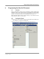
Creating the Project
; The first step is the creation of a project in the Nios IDE. Start the IDE and set
up a workspace at a location on your hard disk.
; Create a new project. Choose New in the file menu and select Project...
MEN Mikro Elektronik GmbH
21F206N00 E1 – 2006-03-10
22
Programming the Nios Soft Processor
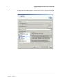
; Choose C/C++ Application in the window and press on Next.
MEN Mikro Elektronik GmbH
21F206N00 E1 – 2006-03-10
23
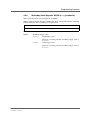
Programming the Nios Soft Processor
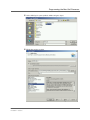
; Choose the Hello LED template. Then in order to select a target hardware click
on Browse.
MEN Mikro Elektronik GmbH
21F206N00 E1 – 2006-03-10
24
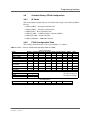
Programming the Nios Soft Processor
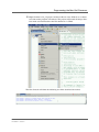
; Select NIOS.ptf in your synthesis folder and press Open.
; Finish the project creation.
MEN Mikro Elektronik GmbH
21F206N00 E1 – 2006-03-10
25
Programming the Nios Soft Processor
6.3
Editing the Source Code
The code needs a bit of editing in order to match a 4 Bit PIO.
; Open the hello_led.c file and change the direction switch condition.
; The LED PIO will switch the direction when reaching the outermost LEDs
now.
6.4
Compiling and Downloading the Program
; Make sure that you have activated the Avalon bus by clearing the reset. This can
be done by writing 0x02 to the Reset Mask Register RMR (0x04) of the reset
controller.
MenMon> cb0 80200404
80200404: 00-> 02
80200404: 02-> q
MenMon>
After the reset is disabled, the Nios tries to boot from SDRAM.
MEN Mikro Elektronik GmbH
21F206N00 E1 – 2006-03-10
26
Programming the Nios Soft Processor
; Right click the hello_led project and choose Run As Nios II Hardware to download and run the program on hardware. The project will be built if changes have
been made and downloaded to the Nios hardware via JTAG.
The Nios Console will show the following text if the download succeeded:
MEN Mikro Elektronik GmbH
21F206N00 E1 – 2006-03-10
27
Appendix
7
Appendix
7.1
Literature and Web Resources
• For up-to-date information on accessories and software for the F206N see the
F206N data sheet on MEN’s website
• WISHBONE System-on-Chip (SoC) Interconnection Architecture for Portable
IP Cores
Revision: B.3, Released: September 7, 2002
www.opencores.org/projects.cgi/web/wishbone/wbspec_b3.pdf
• For more information about Altera’s Nios Processor and Quartus Design Software see www.altera.com/literature
MEN Mikro Elektronik GmbH
21F206N00 E1 – 2006-03-10
28