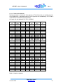
1
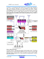
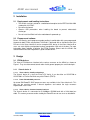
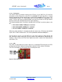
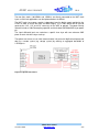
AD481 user manual
V1.1
AD481
User Manual
4DSP Inc, 955 S Virginia Street, Suite 214, Reno, NV 89502, USA
4DSP bv, Crown Business Centre, Leidse Schouw 2, 2408 AE Alphen a/d Rijn, Netherlands
Email: [email protected]
This document is the property of 4DSP Inc. and may not be copied nor communicated to a
third party without the written permission of 4DSP Inc.
© 4DSP 2008
AD481 user manual
V1.1
Revision History
Date
Revision
Version
02-09-07
First release
1.0
05-11-08
Updated the document to reflect the latest state of the
HW
1.1
10-11-08
november 2008
AD481 User manual
www.4dsp.com
-2-
AD481 user manual
V1.1
Table of Contents
1
2
3
4
5
6
7
8
9
Acronyms and related documents ............................................................................. 4
1.1
Acronyms............................................................................................................... 4
1.2
Related Documents ............................................................................................... 4
1.3
General description................................................................................................ 4
Installation ................................................................................................................... 6
2.1
Requirements and handling instructions ................................................................ 6
2.2
Firmware and software........................................................................................... 6
Design .......................................................................................................................... 6
3.1
FPGA devices ........................................................................................................ 6
3.1.1
Virtex-4 device A ............................................................................................ 6
3.1.2
Virtex-4 device B ............................................................................................ 9
3.2
FPGA devices configuration..................................................................................10
3.2.1
Flash storage ................................................................................................10
3.2.2
CPLD device .................................................................................................10
3.2.3
JTAG.............................................................................................................12
3.3
Clock tree..............................................................................................................13
3.4
Memory resources ................................................................................................13
3.4.1
QDR2 SRAM.................................................................................................13
3.4.2
DDR2 SDRAM ..............................................................................................13
3.5
DAC inputs and outputs main characteristics ........................................................14
3.6
DAC connector locations.......................................................................................14
3.7
DAC Clock tree .....................................................................................................16
3.8
Front Panel optical transceivers ............................................................................16
Power requirements ...................................................................................................18
4.1
External power connector for stand alone mode ...................................................19
System Side view........................................................................................................20
Environment................................................................................................................20
6.1
Temperature .........................................................................................................20
6.2
Convection cooling................................................................................................20
6.3
Conduction cooling ...............................................................................................20
Safety...........................................................................................................................20
EMC .............................................................................................................................21
Warranty......................................................................................................................21
november 2008
AD481 User manual
www.4dsp.com
-3-
AD481 user manual
V1.1
1 Acronyms and related documents
1.1
Acronyms
ADC
DAC
DCI
DDR
DSP
EPROM
FBGA
FPDP
FPGA
JTAG
LED
LVTTL
LVDS
LSB
LVDS
MGT
MSB
PCB
PCI
PCI-e
PLL
PMC
QDR
SDRAM
SRAM
Analog to Digital Converter
Digital to Analog Converter
Digitally Controlled Impedance
Double Data Rate
Digital Signal Processing
Erasable Programmable Read-Only Memory
Fineline Ball Grid Array
Front Panel Data Port
Field Programmable Gate Array
Join Test Action Group
Light Emitting Diode
Low Voltage Transistor Logic level
Low Differential Data Signaling
Least Significant Bit(s)
Low Voltage Differential Signaling
Multi-Gigabit Transceiver
Most Significant Bit(s)
Printed Circuit Board
Peripheral Component Interconnect
PCI Express
Phase Locked Loop
PCI Mezzanine Card
Quadruple Data rate
Synchronous Dynamic Random Access memory
Synchronous Random Access memory
Table 1: Glossary
1.2
Related Documents
•
•
•
•
•
•
•
1.3
IEEE Std 1386.1-2001 : IEEE Standard Physical and Environmental Layers for PCI
Mezzanine Cards (PMC).
ANSI/VITA 32-2003 : Processor PMC.
ANSI/VITA 39-2003 : PCI-X for PMC and Processor PMC.
IEEE Std 1386-2001 : IEEE Standard for a Common Mezzanine Card (CMC) Family.
Xilinx Virtex-4 user guide
Xilinx PCI-X core datasheet
Xilinx Virtex-4 Rocket I/O guide
General description
november 2008
AD481 User manual
www.4dsp.com
-4-
AD481 user manual
V1.1
The AD481 is a high performance PMC module with two analogue outputs dedicated to
digital signal processing applications with high bandwidth and complex algorithms
requirements. The AD481 can interface to a PCI-express, PCI-X and/or PCI bus. In addition
to two 1000MSPS DAC channels, the AD481 offers fast on-board memory resources and
two Virtex-4 FPGAs. Up to 4x 2.5Gbps optical transceivers for serial FPDP or gigabit
Ethernet applications are available for communication with external systems. The AD481 is
mechanically and electrically compliant to the standard and specifications listed in section 1.2
of this document.
Figure 1: AD481 block diagram
The AD481 converts 2 14-bit digital data streams into two analogue signals. The digital to
Analogue conversion is performed by the MB86064 Device with a conversion rate up to 1000
MSPS per channel. The clock source can be set to external or internal using the software
and firmware settings available to users. Please note that the clock generation is using lowjitter clock synthesizers.
november 2008
AD481 User manual
www.4dsp.com
-5-
AD481 user manual
V1.1
2 Installation
2.1
Requirements and handling instructions
The AD481 must be installed on a motherboard compliant to the IEEE Std 1386-2001
standard for 3.3V PMC.
Do not flex the board
Observe SSD precautions when handling the board to prevent electrostatic
discharges.
Do not install the AD481 while the motherboard is powered up.
•
•
•
•
2.2
Firmware and software
Drivers, API libraries and a program example working in combination with a pre-programmed
firmware for both FPGAs are provided. The AD481 is delivered with an interface to the Xilinx
PCI core in the Virtex-4 device A and an example VHDL design in the Virtex-4 device B so
users can start digitizing and performing data manipulation right out of the box. For more
information about software installation and FPGA firmware, please refer the AD481 Get
Started Guide and to the Programmer’s guide available online.
3 Design
3.1
FPGA devices
The Virtex-4 FPGA devices interface to the various resources on the AD481 as shown on
Figure 1. They also interconnect to each other via 86 general purpose pins and 2 clock pins.
3.1.1
3.1.1.1
Virtex-4 device A
Virtex-4 device A family and package
The Virtex-4 device A is from the Virtex-4 FX family. It can be either an XC4VFX20 or
XC4VFX60 in a Fineline Ball Grid array with 672 balls (FF672).
3.1.1.2
Power PC embedded processor
Up to two IBM PowerPC RISC processor cores are available in the Virtex-4 device A. This
core can be used to execute C based algorithms and control the logic resources
implemented in the FPGA.
3.1.1.3
Virtex-4 device A external memory interfaces
The Virtex-4 device A is connected to a 128Mbytes SDRAM bank with a 32-bit data bus
width. This memory resource can be used by the PowerPC core or can serve as data buffer.
november 2008
AD481 User manual
www.4dsp.com
-6-
AD481 user manual
3.1.1.4
V1.1
PCI interface
The Virtex-4 device A interfaces directly to the PCI bus via the PMC Pn1, Pn2 and Pn3
connectors or to the PCI-e bus via the Pn5. An embedded PCI core from Xilinx is used to
communicate over the PCI bus with the host system on the motherboard. PCI-e 4 lanes, PCIX 64-bit 66MHz/133MHz, PCI 64-bit 66MHz and PCI 32-bit 33MHz are supported on the
AD481. The bus type must be communicated at the time of the order so the right Virtex-4
device A firmware can be loaded into the flash prior to delivery.
The following performances have been recorded with the AD481 transferring data on the
bus:
PCI-X 64-bit 133MHz: 750Mbytes/s sustained
PCI-X 64-bit 66MHz: 425Mbytes/s sustained
PCI 32-bit 33MHz: 112Mbytes/s sustained
Without any data reduction it is therefore possible to transfer over a PCI-X bus two digitized
signals with a 12-bit resolution each. The resulting bandwidth would be 630Mbytes/s.
The PCI-express 4-lane is using the MGT I/Os on the Virtex-4 device A. Power filtering, low
jitter clock and special routing are used to achieve the performances required by this
standard. Please refer to the Front Panel Optical transceivers section of this document for
more details (3.6).
3.1.1.5
LED
Four LEDs are connected to the Virtex-4 device A. In the default FPGA firmware, the LEDs
are driven by the Virtex-4 device B via the Virtex-4 device A/ Virtex-4 device B interface.
The LEDs are located on side 2 of the PCB in the front panel area.
Figure 2: FPGA LED locations
november 2008
AD481 User manual
www.4dsp.com
-7-
AD481 user manual
3.1.1.6
V1.1
Pn4 user I/O connector
The Pn4 connector is wired to the Virtex-4 device A. The 32 lower bits are available only if an
XC4VFX60 device is mounted on board. The 32 higher bits are available only if PCI 32-bit is
used and only if specified at the time of order.
All signals are user-defined 3.3V LVTLL./LVCMOS.
Connector
pin
1
3
5
7
9
11
13
15
17
19
21
23
25
27
29
31
33
35
37
39
41
43
45
47
49
51
53
55
57
59
61
63
Signal
name
Pn4_IO0
Pn4_IO2
Pn4_IO4
Pn4_IO6
Pn4_IO8
Pn4_IO10
Pn4_IO12
Pn4_IO14
Pn4_IO16
Pn4_IO18
Pn4_IO20
Pn4_IO22
Pn4_IO24
Pn4_IO26
Pn4_IO28
Pn4_IO30
Pn4_IO32
Pn4_IO34
Pn4_IO36
Pn4_IO38
Pn4_IO40
Pn4_IO42
Pn4_IO44
Pn4_IO46
Pn4_IO48
Pn4_IO50
Pn4_IO52
Pn4_IO54
Pn4_IO56
Pn4_IO58
Pn4_IO60
Pn4_IO62
FPGA
pin
M9
N11
N7
N6
P10
P9
R8
R6
N21
M20
P19
N18
P16
R18
P21
R17
L9
L5
AD10
L3
AC11
N4
T8
R5
AB10
R3
Y10
P3
U5
T3
V6
V4
FPGA
pin
M10
M11
N8
P6
P11
N9
P8
R7
M21
M19
N19
N17
N16
P18
P20
R16
M5
AD11
L4
AB11
M4
T9
P5
AA10
P4
W10
N3
U6
T4
U7
U4
U9
Signal
name
Pn4_IO1
Pn4_IO3
Pn4_IO5
Pn4_IO7
Pn4_IO9
Pn4_IO11
Pn4_IO13
Pn4_IO15
Pn4_IO17
Pn4_IO19
Pn4_IO21
Pn4_IO23
Pn4_IO25
Pn4_IO27
Pn4_IO29
Pn4_IO31
Pn4_IO33
Pn4_IO35
Pn4_IO37
Pn4_IO39
Pn4_IO41
Pn4_IO43
Pn4_IO45
Pn4_IO47
Pn4_IO49
Pn4_IO51
Pn4_IO53
Pn4_IO55
Pn4_IO57
Pn4_IO59
Pn4_IO61
Pn4_IO63
Connector
pin
2
4
6
8
10
12
14
16
18
20
22
24
26
28
30
32
34
36
38
40
42
44
46
48
50
52
54
56
58
60
62
64
Table 2 : Pn4 pin assignment
november 2008
AD481 User manual
www.4dsp.com
-8-
AD481 user manual
3.1.2
3.1.2.1
V1.1
Virtex-4 device B
Virtex-4 device B family and package
The Virtex-4 device B is dedicated to interfacing to the A/D circuitry and can also perform
Digital Signal Processing algorithms. It is available in the Virtex-4 SX or LX family devices
and is packaged in a 1148-ball Fineline Ball Grid array. In terms of logic and dedicated DSP
resources, The FPGA B can be chosen in 5 different sizes: SX55, LX40, LX60, LX80, LX100
and LX160.
3.1.2.2
Virtex-4 device B external memory interfaces
The Virtex-4 device B interfaces to four 8Mbytes QDR2 SRAM devices with 32-bit data bus,
Please note that the four QDR2 SRAM devices are only available with the LX80, LX100 and
LX160 devices. For smaller Virtex-4 FPGAs (LX40, LX60 and SX55) only three QDR2 SRAM
devices are connected to the FPGA.
november 2008
AD481 User manual
www.4dsp.com
-9-
AD481 user manual
3.2
V1.1
FPGA devices configuration
3.2.1 Flash storage
The FPGA firmware is stored on board in a flash device. The 128Mbit device is partly
used to store the configuration for both FPGAs. In the default CPLD firmware
configuration, the Virtex-4 devices A and B are directly configured from flash if a valid
bitstream is stored in the flash for each FPGA. The flash is pre-programmed in factory
with the default firmware example for both FPGAs.
Figure 3 : Configuration circuit
3.2.2 CPLD device
As shown on Figure 2, a CPLD is present on board to interface between the flash device and
the FPGA devices. It is of type CoolRunner-II. The CPLD is used to program and read the
flash. The data stored in the flash are transferred from the host motherboard via the PCI bus
to the Virtex-4 device A and then to the CPLD that writes the required bit stream to the
storage device. A 31.25 MHz clock connects to the CPLD and is used to generate the
configuration clock sent to the FPGA devices. At power up, if the CPLD detects that an
FPGA configuration bitstream is stored in the flash for both FPGA devices, it will start
programming the devices in SelectMap mode.
Do NOT reprogram the CPLD without 4DSP approval
The CPLD configuration is achieved by loading with a Xilinx download cable a bitstream from
a host computer via the JTAG connector. The FPGA devices configuration can also be
performed using the JTAG.
3.2.2.1
DIP Switch
A switch (J1) is located next to the JTAG programming connector (J6) see Figure 4. The
switch positions are defined as follows:
november 2008
AD481 User manual
www.4dsp.com
- 10 -
AD481 user manual
V1.1
Figure 4: switch (J1) location
Sw1
OFF
Default setting. The Virtex-4 device A configuration is loaded from the flash at
power up.
ON
Virtex-4 device A safety configuration loaded from the flash at power up. To be
used only if the Virtex-4 device A cannot be configured or does not perform
properly with the switch in the OFF position.
Sw2
Reserved
Sw3
Reserved
Sw4
Reserved
Table 3: Switch description
3.2.2.2
LED and board status
Four LEDs connect to the CPLD and give information about the board status.
LED 0
LED 1
LED 2
LED 3
LED 3
Flashing
FPGA A or B bitstream or user_ROM_register is currently
being written to the flash
ON
FPGA A not configured
OFF
FPGA A configured
Flashing
FPGA A or B bitstream or user_ROM_register is currently
being written to the flash
ON
FPGA B not configured
OFF
FPGA B configured
Flashing
The Virtex-4 device A has been configured with the safety
configuration bitstream programmed in the flash at factory.
Please write a valid Virtex-4 device A bitstream to the flash.
ON
Flash is busy writing or erasing
OFF
Flash device is not busy
ON
CRC error. Presumably a wrong or corrupted FPGA bitstream
has been written to the flash. Once on this LED remains on
OFF
No CRC error detected
Table 4: LED board status
november 2008
AD481 User manual
www.4dsp.com
- 11 -
AD481 user manual
V1.1
Figure 5: CPLD LED locations
3.2.3 JTAG
A JTAG connector is available on the AD481 for configuration purposes. The JTAG can also
be used to debug the FPGA design with the Xilinx Chipscope.
The JTAG connector is located on side 1 of the PCB in front (see Figure 6).
vcc
tms
gnd
tdi
tck
tdo
JTAG connector
Figure 6: JTAG connector (J6) location
The JTAG connector pinout is as follows:
Pin #
1
2
3
Signal
1.8V
GND
TCK
Signal
TMS
TDI
TDO
Pin #
4
5
6
Table 5 : JTAG pin assignment
november 2008
AD481 User manual
www.4dsp.com
- 12 -
AD481 user manual
3.3
V1.1
Clock tree
The AD481 clock architecture offers an efficient distribution of low jitter clocks. In addition to
the PCI Express bus, the MGT reference clocks of 106.25MHz and 125MHz (Epson
EG2121CA) make it possible to implement several standards over the MGT I/Os connected
to the optical transceivers.
Both FPGAs receive a low jitter 125MHz clock. A low jitter programmable clock able to
generate frequencies from 62.5MHz to 255.5MHz in steps of 0.5MHz is also available. This
clock management approach ensures maximum flexibility to efficiently implement multi-clock
domains algorithms and use the memory devices at different frequencies. Both clock buffer
devices (CDM1804) and the frequency synthesizer (ICS8430-61) are controlled by the
Virtex-4 device A.
Figure 7 : Clock tree
3.4
Memory resources
3.4.1 QDR2 SRAM
Four independent QDR2 SRAM devices are connected to the Virtex-4 device B. The QDR2
SRAM devices available on the AD481 are 2M words deep (8Mbytes per memory device).
Please note that only three QDR SRAM devices are available to the user if the XC4VLX40,
XC4VLX60 or XC4VSX55 FPGA device is mounted on board. In this case the mounted
banks are A(0), C(2) and D(3).
3.4.2 DDR2 SDRAM
Two 16-bit DDR2 SDRAM devices of 128MBytes each are connected to Virtex-4 device A.
The two memories share the same address and control bus and have their own data bus.
This memory resource can be accessed by the PowerPC processor in the Virtex-4 device A
or can be used as a data buffer for custom user logic.
november 2008
AD481 User manual
www.4dsp.com
- 13 -
AD481 user manual
3.5
V1.1
DAC inputs and outputs main characteristics
Table 6: AD481 A/D characteristics
Analogue outputs
Output current range
20mA
Data Format
Analogue current
External sampling clock inputs
LVPECL Clock
Signal format
LVPECL
Frequency range
25MHz to 1000 MHz
RF Clock
Signal format
Sinus wave
Frequency range
25MHz to 1000 MHz
Amplitude
0dBm Typ
External trigger inputs
Signal format
LVPECL
Frequency range
DC to 100 MHz
ADC Performance @ Single tone at -1dBFS, 800MSa/s, DC to 400MHz (From DAC datasheet)
Spurious Free Dynamic Range (SFDR) @ 20MHz
75dBc
Spurious Free Dynamic Range (SFDR) @ 300MHz
58dBc
Cross-talk 4 tone test, each tone at -15dBFS, centred at 276MHz
67dBc
3.6
DAC connector locations
The following diagram indicates the location of all the important connectors and components
on the DAC281 PCB.
Figure 8 : DAC281 top view
november 2008
AD481 User manual
www.4dsp.com
- 14 -
AD481 user manual
V1.1
Table 7: DAC281 connector locations
Diagram
Ref
Pcb
RefDes
Description
Notes
A
J11
External Trigger B
Channel
LVPECL Signal. Positive on inside of connector. Negative on outside of
connector.
B
J10
External Trigger A
Channel
LVPECL Signal. Positive on inside of connector. Negative on outside of
connector.
C
J13
DAC Output
Channel (neg)
B
Analog Signal. Signal on inside of connector. GND on outside of connector. For
DC Coupling only (differential signal, split over both connectors).
D
J3
DAC Output
Channel (pos)
B
Analog Signal. Signal on inside of connector. GND on outside of connector. For
AC Coupling (single ended), and pos side of DC coupling (differential)
E
J12
DAC Output
Channel (neg)
A
Analog Signal. Signal on inside of connector. GND on outside of connector. For
DC Coupling only (differential signal, split over both connectors).
F
J2
DAC Output
Channel (pos)
A
Analog Signal. Signal on inside of connector. GND on outside of connector. For
AC Coupling (single ended), and pos side of DC coupling (differential).
G
J1
DAC Test
Output
Clock
LVPECL output test clock. Copy of clock going to DAC. Postive on inside of
connector, negative on outside of connector. Used for verification of the clock
going to the DAC.
H
J5
External RF clock
input
External Analog input Clock to DAC. Clock on inside of connector, DGND on the
outside of connector.
I
J4
External ECL clock
input
External ECL input Clock to DAC. Positive on inside of connector, negative on
the outside of connector.
Table 8: DAC281 component locations
Diagram
Ref
Pcb
RefDes
Description
Notes
J
J8
FPGA
/
MSP
JTAG Connector
FPGA / MSP430 on SMT338-VP JTAG routed down to SMT338-VP. Use for
without having to remove the SMT381.
K
U9
Fujitsu DAC
DAC Requires heat-sink with air-flow system setup.
L
TRANS2
M/A Com TP101
Transformer
By default the SMT381 analog input through a twisted pair balum transformer
single ended). It is possible to change this to DC coupled by taking out the
transformer and installing some resistors on the board.
M
TRANS1
M/A Com TP101
Transformer
By default the SMT381 analog input through a twisted pair balum transformer
single ended). It is possible to change this to DC coupled by taking out the
transformer and installing some resistors on the board.
N
VCO1
UMC
600
1200MHz VCO
System Clock for the DAC. VCO Requires with air-flow cooling in a system
setup.
O
U31
Clock Synthesizer
50 – 950MHz
november 2008
–
Test Clock for DAC. The range of this than the operating range of the DAC.
AD481 User manual
www.4dsp.com
- 15 -
AD481 user manual
3.7
V1.1
DAC Clock tree
The main clock source of the module is an UMC 600MHz to 1200MHz voltage controlled
oscillator. The frequency range of the VCO is adjustable with a frequency synthesizer. The
output of the VCO + Synthesizer combination is passed through a Maxim high frequency
comparator with an LVPECL output to form the main system clock. In addition to this clock
there is a clock synthesizer on the module that can generate a 50 to 950 MHz clock. This
clock is ideal for testing purposes. Alternatively the user can provide the module with an
external LVPECL clock.
Comperator
max9601
10.00Mhz
Oscilator
Lmx2330
Frequency
synthesizer
VCO
600-1200
MHz
16.00Mhz
Oscilator
:2
Fpga_clk0
Divide by 8
&
1:2 buffer
Fpga_clk1
Clock
synthesizer
50-950 MHz
SY89430
DAC clk
Ext
DAC
clk
out
Figure 9: DAC281 clock tree
The clock synthesizer does not offer a clock as good as the VCO does. Therefore the
performances of the module degrade when using the clock synthesizer and it is
recommended to use the VCO whenever possible.
The FPGA controls the LVPECL multiplexers that drive the clock fed to the ADC device
(clock synthesizer, PLL+VCO, or external). The selected clock is distributed to the DAC and
the FPGA on the host module for synchronization purposes. The digital interface works in a
Dual data rate mode, which means that the clock from the DAC to the FPGA runs at half the
conversion frequency.
3.8
Front Panel optical transceivers
Four 2.5Gb/s optical transceivers (LTP-ST11M) are available on the AD481 in the front panel
area. They are connected to the MGT I/Os of the Virtex-4 device A. Infiniband protocols as
well as Gigabit Ethernet and Fibre channel (sFPDP) can be implemented over the
transceivers. Lower rate optical transceivers (2.125Gb/s and 1.0625Gb/s) are available in the
same form factor.
november 2008
AD481 User manual
www.4dsp.com
- 16 -
AD481 user manual
V1.1
Two low jitter clocks (106.25MHz and 125MHz) are directly connected to the MGT clock
inputs so multi-rate applications can be implemented on the AD481.
The MGT banks have power supplies independent from the digital supply provided to the
FPGAs in order to insure low noise and data integrity. The LT1963 device will be used to
generate the 1.2V, 1.5V and 2.5V necessary for the MGT to operate. The power filtering
network includes a 220nF decoupling capacitor and ferrite bead (MP21608S221A) per power
pin.
The signal differential pairs are routed on a specific inner layer with one reference GND
plane on each side of the layer stack up.
The optical transceivers are an ideal communication link to transfer digitized and processed
data to a remote system (eg, storage system) by offering an aggregate bandwidth of
1.25GBytes/s.
Figure 10: Optical transceivers
november 2008
AD481 User manual
www.4dsp.com
- 17 -
AD481 user manual
V1.1
4 Power requirements
The power is supplied to the AD481 via the PMC connectors. Several DC-DC converters
generate the appropriate voltage rails for the different devices and interfaces present on
board.
The AD481 power consumption depends mainly on the FPGA devices work load. By using
high efficiency power converters, all care has been taken to ensure that power consumption
will remain as low as possible for any given algorithm.
After power up, the AD481 typically consumes 5W of power. For precise power
measurements it is recommended to use the Xilinx power estimation tools for both FPGA A
and B. The maximum current rating given in the table below is the maximum current that can
be drawn from each voltage rail in the case where resources are used to their maximum
level.
Device/Interface
Voltage
Maximum
current rating
0.9V
5A
Virtex-4 device A & B core
1.2V
12A
QDR2, DDR2 SDRAM core and
I/O banks, Virtex-4 devices I/O
banks
1.8V
10A
Virtex-4 device B I/O bank
connected to the front panel
daughter card
1.8V/2.5/3.3V
1.5A
Virtex-4 device A I/O bank
connected to the PCI bus, Flash,
CPLD, front Panel I/O daughter
card, A/D circuitry
3.3V
4A
1.2V, 1.5V, 2.5V
1.7A, 0.5A, 0.01A
respectively
DCI and
voltage
memory
MGT power supply
reference
Table 9 : Power supply
november 2008
AD481 User manual
www.4dsp.com
- 18 -
AD481 user manual
V1.1
Figure 11 : Power supply
An ADT7411 device is used to monitor the power on the different voltage rails as well as the
temperature. The ADT7411 data are constantly passed to the Virtex-4 device A.
Measurements can be accessed from the host computer via the PCI bus. A software utility
delivered with the board allows the monitoring of the voltage on the 2.5V, 1.8V, 1.2V and
0.9V rails. It also displays the Virtex-4 device B junction temperature.
4.1
External power connector for stand alone mode
An external power connector (J2) is available on side 2 of the PMC, next to the PMC
connectors. It is used to power the board when it is in stand alone mode. This is a right
angled connector and it will be mounted on board only if the card is ordered in its stand alone
version (AD481-SA). The height and placement of this connector on the PCB breaches the
PMC specifications and the module should not be used in an enclosed chassis compliant to
PMC specifications if the external power connector is present on board.
Do not connect an external power source to J2 if the board is powered via the
PMC connectors. Doing so will result in damaging the board.
The external power connector is of type Molex 43045-1021. Each circuit can carry a
maximum current of 5A. The connector pin assignment is as follows:
Pin #
1
3
5
7
9
Signal
3.3V
5V
GND
GND
-12V
Signal
3.3V
5V
GND
GND
12V
Pin #
2
4
6
8
10
Table 10 : External power connector pin assignment
november 2008
AD481 User manual
www.4dsp.com
- 19 -
AD481 user manual
V1.1
5 System Side view
The following diagram shows a side view of the AD481 mounted a motherboard.
Figure 12: System side view
6 Environment
6.1
Temperature
Operating temperature
• 0°C to +60°C (Commercial)
• -40°C to +85°C (Industrial)
Storage temperature:
• -40°C to +120°C
6.2
Convection cooling
600LFM minimum
6.3
Conduction cooling
The AD481 can optionally be delivered as conduction cooled PMC. The AD481 is compliant
to ANSI/VITA 20-2001 standard for conduction cooled PMC.
7 Safety
This module presents no hazard to the user.
november 2008
AD481 User manual
www.4dsp.com
- 20 -
AD481 user manual
V1.1
8 EMC
This module is designed to operate from within an enclosed host system, which is build to
provide EMC shielding. Operation within the EU EMC guidelines is not guaranteed unless it
is installed within an adequate host system. This module is protected from damage by fast
voltage transients originating from outside the host system which may be introduced through
the system.
9 Warranty
Hardware
Software/Firmware
Basic Warranty (included)
1 Year from Date of Shipment
90 Days from Date of Shipment
Extended Warranty (optional)
2 Years from Date of Shipment
1 Year from Date of Shipment
november 2008
AD481 User manual
www.4dsp.com
- 21 -