1
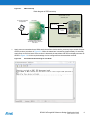
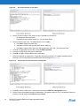
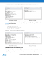
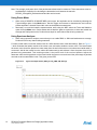
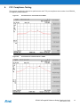
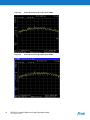
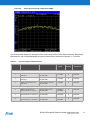
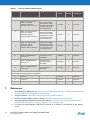
APPLICATION NOTE Atmel AT04467: Wireless SoC Reference Design with RFMDs RF6555 NOT RECOMMENDED FOR NEW DESIGNS Atmel MCU Wireless Description The RF6555_ATmega_256_Referenceboard is a reference design developed by the partnership between RFMD and Atmel® Corporation. This design presents a complete solution using a 2.4GHz ZigBee® IEEE® 802.15.4 based compliant radio transceiver solution that conforms to FCC CFR47 part 15. Atmel introduces the ATmega256RFR2 as its ZigBee platform which features a low power 2.4GHz radio frequency transceiver and a high performance, low power AVR®, 8-bit microcontroller delivered as a 9mm x9 mm x 0.9mm 64-pin QFN package. RFMD presents a world class Front End Module (FEM), the RF6555 for efficient extended output power beyond 18dBm with harmonic filtering, diversity switch, and LNA with bypass. Features Output power +18dBm (0.063 Watt) Industry leading 129dB link budget Low harmonic content Antenna diversity RoHS compliant Single differential bidirectional TX/RX interface 42262A-WIRELESS-04/2014 1. Overview This application note provides information about the evaluation and analysis of the data and design tools for implementing a ZigBee solution using the RF6555 ATmega256 Reference board. The RF6555 [2] FEM is a medium power (14 to 18dBm) Smart Energy front end solution available on a singlechip. It integrates the PA with harmonic filtering, LNA with bypass, SPDT switch for TX/RX functionality, DP2T switch for antenna diversity and a 100 ohm Balun for single differential bidirectional TX/RX interface all on a single 5mm x 5mm x 0.975mm VQFN 24-Pin package. The RF6555_ATmega256_Referenceboard design is a proven range extension for the Atmega256RFR2 with a link budget of 103.5dBm. The RF6505, RFFM6201, RF6545, and RF6575 [3] also serves as range extensions for the ATmega128RFA1, ATmega256RFR2 [1] and AT86RF231 radio transceivers. This reference board is pre-flashed with the performance test EVK application from MAC 2.8.0 stack software interface to allow performance verification. This reference board is available for purchase at RFMD Online Store (www.rfmd.com). Contact RFMD Technical Support at [email protected]. 2. Applications This reference board design can be used for: 3. ZigBee 802.15.4 based systems for Remote Monitoring and Control Communications Hub for Smart Energy/Home Automation Smart meters for Energy Management Functional Descriptions Interfacing -The RF6555_ATmega256_Referenceboard is equipped with two 50mil, 30-pin connectors (EXT0/1) that are placed parallel to each other 22mm apart. These are for interfacing with the STB. EEPROM - An EEPROM is provided on the RF6555_ATmega256_Referenceboard to identify the transceiver and software. It stores the production calibration and MAC address information. This EEPROM might not be required on the final product, after completing the user design. RF Communications - The RF6555_ATmega256_Referenceboards are equipped with two PCB antennas A1 and A2 used for antenna diversity for over-the-air testing. A SMA female connector X1, which is Digi-Key P/N J500-ND is used for conducted measurements. Supports conducted testing using J1, an MS-147 receptacle which is Digi-Key P/N H2800DKR-ND that mates to Digi-Key P/N H2802-ND. 4. Mechanical Descriptions The RF6555_ATmega256_Referenceboard contains a 4-layer design on standard FR4 material (IS400) with a total thickness of 66 mils. It can be designed on a 2-layer board [4]. The top and bottom layers are large copper planes with their grounds stitched together with through-hole vias placed close to the GND pins of critical RF components [4]. 1. 2. 3. 2 The top layer contains a solid 1oz base copper and plating for digital ground plane. It is used for RF and digital signal routing and contains an isolation between the digital and RF traces. The middle layer 1 is a solid digital ground. The middle layer 2 is an internal layer and a solid power plane with nets to VCC and V_RCB. The power plane should be surrounded with through-hole ground vias that connect the ground layers. RF6555 ATmega256 Reference Design [Application Note] 42262A-WIRELESS-04/2014 4. The bottom layer is a digital ground plane shared with RF and made using solid 1oz base copper and plating. The filter-balun B1 requires a solid ground connection. See Figure 4-1 for layer stack-up details. Figure 4-1. RF6555_ATMmega256_Referenceboard Layer Stack-Up Note: It is highly recommended to follow the PCB layout as close as possible. Deviations from the layout can alter the performance of the reference design. Shielding - The reference design does not contain a metal shield. However, it might be necessary to protect the ICs from external noise and strong interference. Such shields may suppress radiated harmonics from the reference design but is not necessary. The recommended size for the metal shield is 30mm x 25mm. RF Layout Optimization - The RF6555 ground pad contains a 4 x 4 via pattern (See Figure 4-2), with through-hole vias that route from the top layer to the bottom layer. The size of via hole is 12mils and the diameter is 24mils. These specifications enhance thermal dissipation and provides a short return path for the signal. In the final product, the solder mask or solder resist can be removed from the bottom layer beneath the ground pad for improved thermal dissipation. Figure 4-2. RF6555 Ground Slug Via Pattern RF6555 ATmega256 Reference Design [Application Note] 42262A-WIRELESS-04/2014 3 5. Evaluation and Configuration Equipment needed for evaluation Atmel RCB Sensor Terminal Board (STB) [6] Signal or Spectrum analyzer for conducted measurements Computer with a terminal emulator application SMA MS-147 Cables (2) USB cable (if using STB) Power meter Evaluation Board The RF6555_ATmega256_Referenceboard is evaluated on the Atmel RCB Sensor Terminal Board (Figure 51). The Sensor Terminal Board (STB) establishes a USB-based UART connection, programming interfaces, and provides RCB power supply using the USB cable. Ordering information for the STB, descriptions, technical data, documentation, and drivers are available at http://www.dresden-elektronik.de/funktechnik/products/boards-and-kits/development-boards/. Figure 5-1. Sensor Terminal Board Configuration To configure the RF6555_ATmega256_Referenceboard mounted on the STB, connect the STB and the host computer using a USB cable. RCBs may be evaluated using on-board antennas A1 and A2, or by placing SMA connectors on J1 (MS-147) for Antenna 1, or X1 for Antenna 2. Note: RF6555_ATmega256_Referenceboards are shipped with connector X1 out-of-circuit. To evaluate the demo board using connector X1, 4 populate R14 with a 0ohm 0402 resistor remove resistor R13 (located between X1 and balun) RF6555 ATmega256 Reference Design [Application Note] 42262A-WIRELESS-04/2014 Steps for installing and configuring the demo board: If you are using a Sensor Terminal Board, connect the cable to X2 of the STB. Depending on your operating system the driver software for the STB may automatically install. If the installation does not start automatically, download the necessary driver from www.ftdichip.com/Products/ICs/FT245R.htm. After installing the driver, note the COM port number assigned for the device (Illustrated in Figure 5-2). Figure 5-2. 5. Device Manager after Driver Installation The maximum current is limited to 400mA by the on-board voltage regulator in the Sensor Terminal Board. An external power source is not required to achieve full RF power using the RF6555_ATmega256. Figure 5-3. USB Port Settings RF6555 ATmega256 Reference Design [Application Note] 42262A-WIRELESS-04/2014 5 6. Configure the following settings in the relevant COM port (Port Settings tab in Figure 5-3): Baud (Bits per second): 9600 Parity: None Data Bits: 8 Stop Bits: 1 Flow Control: None 7. 8. To establish a connection between the RF6555_ATmega256_Referenceboard and enable the test menu options, configure the terminal emulator application with the COM port settings specified in previous step. Press any key (send ASCII character) to establish communication with the RF6555_ATmega256_Referenceboard. Note: After establishing a connection with the computer terminal, the RF6555_ATmega256_Referenceboard searches for a peer device. This feature allows the remote RF6555_ATmega256_Referenceboard to operate without a computer terminal. For transmission performance testing (single node) mode, press the Enter key on the computer to skip this search. The main menu for the Transmission Performance Evaluation section is displayed as shown in Figure 5-4. If a peer device is detected, both the devices assume PER testing mode. Screen is displayed as in Figure 5-9. The Transmitter Terminal screen is the main menu for the PER Evaluation section. Figure 5-4. 6 RF6555_ATmega256_Referenceboard Terminal Emulator Main Menu RF6555 ATmega256 Reference Design [Application Note] 42262A-WIRELESS-04/2014 5.1 Transmission Performance Evaluation Steps for transmission verification test setup: 1. From the single-node main menu, press 1 to enter the Transceiver Configuration menu. Figure 5-5. 2. 3. 4. Transceiver Configuration Menu Screen Set the channel number for the channel to be tested. By default channel 21 is tested. To change the default channel press C, type channel number (11…26) and press Enter. Set the Transmission Power level. The default is 20dBm. a. Press W to change the power level. b. Press A for absolute and type the power level in dBm (or) c. Press R for register value; type a two digit hexadecimal value (00…0F) and press Enter. Press Y to select antenna, and enter 1 or 2. Press Y again to re-enable Antenna diversity wherein both antennas are used. Note: Antenna diversity should be disabled while validating only one antenna. 5. 6. Press O to exit the Transceiver Configuration menu. From the Main menu, press 2 to enter Transceiver State Selection menu (Figure 5-6). RF6555 ATmega256 Reference Design [Application Note] 42262A-WIRELESS-04/2014 7 Figure 5-6. 7. 8. Transceiver State Selection Menu Screen Set Antenna diversity if it has not been configured earlier. This setting can be configured similar to the Transceiver Configuration menu. Press U to start transmission. Select C for continuous waveform or Select P for modulated (Pseudo Random Binary Sequence) waveform. The demo board is transmitting a signal. 9. 5.2 Press any key to terminate transmission. Packet Error Rate (PER) Evaluation Two RF6555_ATmega256_Referenceboards are required to perform PER testing. The setup is shown in Figure 5-7. One board acts as a transmitter and requires a computer terminal. Another board acts as receiver for which a computer terminal is optional. 8 RF6555 ATmega256 Reference Design [Application Note] 42262A-WIRELESS-04/2014 Figure 5-7. PER Test Setup Block diagram of PER test setup Everything in the box indicates inside a screen (Shielded) room PC running Performance test application Transmitter Receiver Coaxial cable to ANT Variable Attenuator 2.0 to 3.6VDC Voltage Supply or AA batteries USB Cable + RF6555_ATMega256_Reference board connected to battery terminal set as Peer device (Reflector) RF6555_ATMega256_Reference board connected to Sensor Terminal Board set to search for Peer device 1. Apply power to transmitter board. With terminal emulator window active, press any key to search for peer device (receiver) as shown in Figure 5-8. While the transmitter is searching (approximately 12 seconds), apply power to receiver board. If the receiver is detected, the transmitter and receiver displays screens as shown in Figure 5-9. All the required settings can be configured from the transmitter terminal. Figure 5-8. Transmitter Node Searching for Peer Node RF6555 ATmega256 Reference Design [Application Note] 42262A-WIRELESS-04/2014 9 Figure 5-9. 2. 3. 4. 5. 6. 7. Set the Channel number to the channel to test. The default is Channel 21. ̶ To change the channel press C ̶ Type the two digit channel number (11...26) and press Enter. Set the transmit power level. The default power level is 20dBm. a. Press W to change the power level. b. Press A for absolute and type the power level in dBm (or) c. Press R for register value; type a two digit hexadecimal value (00…0F) and press Enter. Press A, to Toggle ACK request until it reads no ACK requested. Press F, to Toggle Frame retry until it reads false. Press M, to Toggle CSMA enabled until it reads false. Select the antenna for transmission. Toggle the antenna by pressing Y. To validate, disable antenna diversity in a Receiving antenna and select that particular antenna Figure 5-10. Figure 5-10. 8. 9. 10 Successful Detection of Peer Node Terminal Screens after Transceiver Configuration Press O to return to Main menu. Then press 3 to enter the PER-Test Configuration menu. Set the number of packets (frames) for transmission. The default number is 100. To change the number of packets, press N, specify the number and press Enter. RF6555 ATmega256 Reference Design [Application Note] 42262A-WIRELESS-04/2014 10. Select the antenna for reception by pressing Q, followed by C and then 2 or 3. Refer Figure 5-11. Figure 5-11. Terminal Screens after Receiver Configuration In the main menu, press 5 and the text Transmitting… Wait until test is completed is displayed on the screen. The main screen displays the number of packets (frames) received. This defines your PER value. See Figure 5-12 for more information. For example, 1000/1000 equates to a 0% PER… 990/1000 equates to 1% PER. Average PER < 1% at -100dBm. Figure 5-12. Terminal Screens after PER Test Transmission PER Radio to Radio Manual Station set up For an instance of radio to radio conducted PER measurements, set the board that transmits packets in its minimum power level. This ensures that the EVM is at a low level and to minimize the number of attenuators required. Start transmitting packets and use either a power meter or a spectrum analyzer to measure the amplitude of the packets. RF6555 ATmega256 Reference Design [Application Note] 42262A-WIRELESS-04/2014 11 Note: The average, peak power level of the packets transmitted must be measured. This measurement must be considered as a baseline for calculating the attenuation level between the transmit RF6555_ATmega256_Referenceboard and the receive board. Using Power Meter When using a ROHDE & SCHWARZ NRP power meter, the amplitude can be recorded by selecting the T’gate Average option in the Mode menu. Set the Trigger and increase or decrease the level until the packet amplitude is located. Record this value as the baseline measurement. Alternately, to record the baseline measurements, while using the NRP, select the Trace and Statistics option from the Mode menu. Select Gates and set both the gates to capture the on-burst and record the Average and Peak power levels. Perform these steps for each channel that is being measured. Using Spectrum Analyzer When using a spectrum analyzer, ensure that you use a wide RBW i.e. 3MHz and set detector to average. Perform this for every channel being measured. For each coaxial cable, record the insertion loss at 2.4GHz and the value of the attenuator(s). Refer to Figure 57 which illustrates the cables outside of the screen room and cables inside the screen room. The board inside the screen room should be placed one meter away from the wall of the screen room where the outside cable is connected. Add all the losses from the cables and attenuator(s) and subtract it from the power level of the packets being transmitted. This resulting number is the power level of the received packets. Adjust the attenuator while receiving packets on the board inside the screen room and record the percentage of packets received at various attenuation levels. This gives you the PER. Figure 5-13. 12 Typical TX Output Power (dBm) per TX_PWR, CW, Settings RF6555 ATmega256 Reference Design [Application Note] 42262A-WIRELESS-04/2014 6. FCC Compliance Testing This section provides the harmonics performance and FCC pre-compliance test results of the RF6555_ ATmega256_Referenceboard. Figure 6-1. Second Harmonic Conducted Pout=18dBm Figure 6-2. Third Harmonic Conducted Pout = 18dBm RF6555 ATmega256 Reference Design [Application Note] 42262A-WIRELESS-04/2014 13 14 Figure 6-3. Power Spectral Density at CH11 Pout=18dBm Figure 6-4. Power Spectral Density at CH19 Pout=18dBm RF6555 ATmega256 Reference Design [Application Note] 42262A-WIRELESS-04/2014 Figure 6-5. Power Spectral Density at CH25 Pout=18dBm The following table displays the test results of the various tests such as Power Spectral Density, Band Edges Measurement, and Occupied Bandwidth using the measurements conducted on channels 11,19, and 25. Table 6-1. FCC Pre-compliance Measurements S.No Test Case Expected Result Measured Value Power Setting Measurement Conditions FCC Compliance [5] 1 Measure the Peak Power on channel 11 Power measured should be less than 30dB 21.74dBm 21 Conducted 2 Measure the Peak Power on channel 19 Power measured should be less than 30dB 21.90dBm 21 Conducted 3 Measure the Peak Power on channel 25 Power measured should be less than 30dB 21.86dBm 21 Conducted Peak Power Spectral Density (PSD) 4 Measure the Peak Power Spectral Density on channel 11 Measure PSD should be less than 8dBm 6.64dBm at 3kHz RBW 21 Conducted 5 Measure the Peak Power Spectral Density on channel 19 Measure PSD should be less than 8dBm 5.06dBm at 3kHz RBW 21 Conducted 6 Measure the Peak Power Spectral Density on channel 25 Measure PSD should be less than 8dBm 4.375dBm at 3kHz RBW 21 Conducted RF6555 ATmega256 Reference Design [Application Note] 42262A-WIRELESS-04/2014 15 Table 6-1. FCC Pre-compliance Measurements S.No Test Case Expected Result Measured Value Power Setting Measurement Conditions Band Edges Measurement Measure the radio Frequency power in the 100kHz bandwidth outside the frequency bands in channel 11 The radio frequency power should be at least 20dB below that in the 100kHz bandwidth within the band that contains the highest level of desired power 40.76dBc 21 Conducted Measure the radio Frequency power in the 100kHz bandwidth outside the frequency bands in channel 19 The radio frequency power should be at least 20dB below that in the 100kHz bandwidth within the band that contains the highest level of desired power 48.67dBc 21 Conducted Measure the radio Frequency power in the 100kHz bandwidth outside the frequency bands in channel 25 The radio frequency power should be at least 20dB below that in the 100kHz bandwidth within the band that contains the highest level of desired power 50.00dBc 21 Conducted 10 Measure the 6dB Bandwidth on channel 11 The minimum 6dB bandwidth should be at least 500kHz 1.4925MHz 21 Conducted 11 Measure the 6dB Bandwidth on channel 19 The minimum 6dB bandwidth should be at least 500kHz 1.5825MHz 21 Conducted 12 Measure the 6dB Bandwidth on channel 25 The minimum 6dB bandwidth should be at least 500kHz 1.5000MHz 21 Conducted 7 8 9 6db Bandwidth Occupied Bandwidth: Bandwidth containing 99% of the total integrated power of the transmitted spectrum, centered on the assigned channel frequency is measured. 7. Channel 11 - 2.310MHz 21 Conducted 14 Channel 19 - 2.367MHz 21 Conducted 15 Channel 25 - 2.370MHz 21 Conducted References 1. 2. 3. 4. 5. 16 13 ATmega256RFR2 Datasheet, http://www.atmel.in/Images/Atmel-8393-MCU_Wireless-ATmega256RFR2ATmega128RFR2 -ATmega64RFR2_Datasheet.pdf RF6555 Datasheet, http://www.rfmd.com/CS/Documents/RF6555DS.pdf RF6575+ATmega128RFA1 reference design, http://www.rfmd.com/atmel/zigbeerf.aspx Atmel AVR10004 RCB256RF2-Hardware User Manual, http://www.atmel.com/Images/Atmel-42081RCB256RFR2-Hardware-User-Manual_Application-Note_AVR10004.pdf FCC Code of Federal Register (CFR); Part 47; Section 15.35, Section 15.205, Section 15.209, Section 15.231, RF6555 ATmega256 Reference Design [Application Note] 42262A-WIRELESS-04/2014 6. Sensor terminal board: www.dresden-elektronik.de/funktechnik/service/download/documentation/ ?L=1#c3646 RF6555 ATmega256 Reference Design [Application Note] 42262A-WIRELESS-04/2014 17 8. 18 Revision History Doc. Rev. Date Rev. A 04/2014 Comments Initial document release. RF6555 ATmega256 Reference Design [Application Note] 42262A-WIRELESS-04/2014 XXXXXX Atmel Corporation 1600 Technology Drive, San Jose, CA 95110 USA T: (+1)(408) 441.0311 F: (+1)(408) 436.4200 | www.atmel.com © 2014 Atmel Corporation. / Rev.A: Atmel-42262A-WIRELESS-RF6555 ATmega256 Reference Design-ApplicationNote_04/2014. Atmel®, Atmel logo and combinations thereof, AVR®, Enabling Unlimited Possibilities®, and others are registered trademarks or trademarks of Atmel Corporation or its subsidiaries. Other terms and product names may be trademarks of others. DISCLAIMER: The information in this document is provided in connection with Atmel products. No license, express or implied, by estoppel or otherwise, to any intellectual property right is granted by this document or in connection with the sale of Atmel products. EXCEPT AS SET FORTH IN THE ATMEL TERMS AND CONDITIONS OF SALES LOCATED ON THE ATMEL WEBSITE, ATMEL ASSUMES NO LIABILITY WHATSOEVER AND DISCLAIMS ANY EXPRESS, IMPLIED OR STATUTORY WARRANTY RELATING TO ITS PRODUCTS INCLUDING, BUT NOT LIMITED TO, THE IMPLIED WARRANTY OF MERCHANTABILITY, FITNESS FOR A PARTICULAR PURPOSE, OR NON-INFRINGEMENT. IN NO EVENT SHALL ATMEL BE LIABLE FOR ANY DIRECT, INDIRECT, CONSEQUENTIAL, PUNITIVE, SPECIAL OR INCIDENTAL DAMAGES (INCLUDING, WITHOUT LIMITATION, DAMAGES FOR LOSS AND PROFITS, BUSINESS INTERRUPTION, OR LOSS OF INFORMATION) ARISING OUT OF THE USE OR INABILITY TO USE THIS DOCUMENT, EVEN IF ATMEL HAS BEEN ADVISED OF THE POSSIBILITY OF SUCH DAMAGES. Atmel makes no representations or warranties with respect to the accuracy or completeness of the contents of this document and reserves the right to make changes to specifications and products descriptions at any time without notice. Atmel does not make any commitment to update the information contained herein. Unless specifically provided otherwise, Atmel products are not suitable for, and shall not be used in, automotive applications. Atmel products are not intended, authorized, or warranted for use as components in applications intended to support or sustain life. SAFETY-CRITICAL, MILITARY, AND AUTOMOTIVE APPLICATIONS DISCLAIMER: Atmel products are not designed for and will not be used in connection with any applications where the failure of such products would reasonably be expected to result in significant personal injury or death (“Safety-Critical Applications”) without an Atmel officer's specific written consent. Safety-Critical Applications include, without limitation, life support devices and systems, equipment or systems for the operation of nuclear facilities and weapons systems. Atmel products are not designed nor intended for use in military or aerospace applications or environments unless specifically designated by Atmel as military-grade. Atmel products are not designed nor intended for use in automotive applications unless specifically designated by Atmel as automotive-grade.