1
• SAFETY PRECAUTIONS •
(Read these precautions before using.)
Before using this product, please read this manual and the relevant manuals introduced in this manual
carefully and pay full attention to safety to handle the product correctly.
The instructions given in this manual are concerned with this product. For the safety instructions of the
programmable controller system, please read the user's manual of the CPU module used.
In this manual, the safety instructions are ranked as "DANGER" and "CAUTION".
DANGER
Indicates that incorrect handling may cause hazardous conditions,
resulting in death or severe injury.
! CAUTION
Indicates that incorrect handling may cause hazardous conditions,
resulting in medium or slight personal injury or physical damage.
!
Note that the ! CAUTION level may lead to a serious consequence according to the circumstances.
Always follow the instructions of both levels because they are important to personal safety.
Please save this manual to make it accessible when required and always forward it to the end user.
[DESIGN PRECAUTIONS]
!
DANGER
• When a communication error occurs on PROFIBUS-DP, the status of the faulty station is as
follows. Configure an interlock circuit in the sequence program using the communication status
information (input X1) so that the system can operate safely.
Erroneous outputs and mis-operation could cause accidents.
(1) The input data from the master station remains unchanged from the data prior to the
communication error.
(2) When the master station becomes faulty, the output status of the QJ71PB93D will be as in
the parameter settings of the master station.
(3) When any QJ71PB93D is down, the output state of other slave stations will be in
accordance with the parameter settings of the master station.
• Do not output (turn on) the "Use prohibited" signal as the output signal to an intelligent function
module from the CPU module.
Writing data into the "system area" or outputting a signal for "Use prohibited" may cause system
malfunction in the programmable controller.
!
CAUTION
• When the PROFIBUS cable is laid, do not lay it close to main circuits or power lines.
They should be installed 100mm(3.9inch) or more from each other.
Not doing so could result in noise that would cause malfunctioning.
A-1
A-1
[INSTALLATION PRECAUTIONS]
!
CAUTION
• Use the programmable controller under the environment specified in the user's manual of the
CPU module to be used.
Otherwise, it may cause electric shocks, fires, malfunctions, product deterioration or damage.
• While pressing the installation lever located at the bottom of the module, insert the module fixing
projection into the fixing hole in the base unit to mount the module.
Incorrect mounting may cause malfunctions, a failure or a drop of the module.
In an environment of frequent vibrations, secure the module with the screw.
• Tighten the screws within the range of specified torque.
If the screws are loose, it may cause the module to fallout, short circuits, or malfunction.
If the screws are tightened too much, it may cause damage to the screw and/or the module,
resulting in fallout, short circuits or malfunction.
• Be sure to shut off all phases of the external power supply used by the system before mounting
or removing the module.
Failure to do so may damage the module.
• Do not touch the conductive area or electric parts of the module.
Doing so may cause module malfunctioning or breakdowns.
[WIRING PRECAUTIONS]
!
CAUTION
• Be sure to shut off all phases of the external power supply used by the system before wiring
PROFIBUS cables.
Failure to do so may result in failure or malfunctions of the module.
• Be careful not to let foreign matter such as filings or wire chips get inside the module. These can
cause fire, breakdowns and malfunctioning.
• Be sure to place the PROFIBUS cables in a duct or clamp them.
If not, dangling cables may be shifted or inadvertently pulled, resulting in damages to the
module or cables or malfunctions due to poor cable contact.
• When disconnecting the PROFIBUS cable from the module, do not pull by holding the cable
section. To disconnect the cable, make sure to hold the connector which is coupled with the
module. Do not attempt to pull the cable to disconnect it from the module. It could damage the
module or the cable, or cause malfunction due to a poor contact of the cable.
• A protective film is attached onto the module top to prevent foreign matter such as wire chips
from entering the module when wiring.
Do not remove the film during wiring.
Remove it for heat dissipation before system operation.
A-2
A-2
[STARTING AND MAINTENANCE PRECAUTIONS]
!
DANGER
• Before cleaning, be sure to shut off all phases of the external power supply used by the system.
Failure to do so may cause electrical shocks.
!
CAUTION
• Never disassemble or modify the module.
This may cause breakdowns, malfunctioning, injury and/or fire.
• When using a wireless communication device such as a cellular phone, keep a distance of
25cm (9.85 inch) or more from the programmable controller in all directions. Failure to do so can
cause a malfunction.
• Be sure to shut off all phases of the external power supply before mounting or removing the
module.
Failure to do so may result in failure or malfunctions of the module.
• Do not mount/remove the module onto/from the base unit more than 50 times (IEC 61131-2
compliant), after the first use of the product.
Failure to do so may cause the module to malfunction due to poor contact of connector.
• Before handling the module, always touch grounded metal, etc. to discharge static electricity
from the human body.
Failure to do so can cause the module to fail or malfunction.
[DISPOSAL PRECAUTIONS]
!
CAUTION
• When disposing of this product, treat it as industrial waste.
A-3
A-3
REVISIONS
* The manual number is given on the bottom left of the back cover.
Print Date
Mar., 2002
Apr., 2004
* Manual Number
SH(NA)-080318E-A First Edition
SH(NA)-080318E-B Correction
Revision
Section 2.1, 2.3, 3.1, 3.3.2, 3.5, 5.2.1, 7.3.1, 7.3.2, 9.5
Addition
Aug., 2004
SAFETY PRECAUTIONS
SH(NA)-080318E-C Correction
Aug., 2006
SAFETY PRECAUTIONS, Section 5.2.1, Chapter 7, Section 8.1, 8.2
SH(NA)-080318E-D Correction
SAFETY PRECAUTIONS, Conformation to the EMC Directive and Low
Voltage Instruction, Section 2.3, 3.1 to 3.5, 5.1, 5.5, 5.7.2, 8.1, 8.2, 9.5,
Appendix 2
Addition
About Manuals, About the Generic Terms and Abbreviations, Meanings
and Definitions of Terms, Section 1.1, 2.1, 2.2, 4.1.1 to 4.1.4, 5.2.1 to
5.2.3, 5.6, 5.7.1, Chapter 6, Section 6.1, 6.2, 7.1 to 7.4, Chapter 8,
Appendix 1
New Addition
Section 5.3
Section number change
Section 3.5 5.2, 3.5.1 to 3.5.3
5.2, 5.2 to 5.5 5.4 to 5.7
Jul., 2007
5.2.1 to 5.2.3, 3.6
3.5, 5.1.1
SH(NA)-080318E-E Change of a term
"PLC" was changed to "programmable controller".
Correction
About the Generic Terms and Abbreviations, Section 2.1, 2.3, 3.1,
3.4.1, 5.5, 8.2 to 8.3, Appendix 1
Addition
Section 5.3.1, 5.4.1, 7.3.1, 7.3.2, 9.4
Section number change
Chapter 8(3)
Nov., 2007
SH(NA)-080318E-F
Section 8.1, Section 8.1 to 8.2
8.2 to 8.3
Correction
Section 3.3.2, 3.4.1, 7.3.1
Japanese Manual Version SH-080317-E
This manual confers no industrial property rights or any rights of any other kind, nor does it confer any patent
licenses. Mitsubishi Electric Corporation cannot be held responsible for any problems involving industrial property
rights which may occur as a result of using the contents noted in this manual.
© 2002 MITSUBISHI ELECTRIC CORPORATION
A-4
A-4
INTRODUCTION
Thank you for purchasing the Mitsubishi Programmable Controller MELSEC-Q Series.
Before using the equipment, please read this manual carefully to develop full familiarity with the functions
and performance of the graphic operation terminal you have purchased, so as to ensure correct use.
Please forward a copy of this manual to the end user.
CONTENTS
SAFETY PRECAUTIONS.............................................................................................................................A - 1
REVISIONS ...................................................................................................................................................A - 4
INTRODUCTION...........................................................................................................................................A - 5
CONTENTS...................................................................................................................................................A - 5
About Manuals ..............................................................................................................................................A - 7
Conformation to the EMC Directive and Low Voltage Instruction ...............................................................A - 7
About the Generic Terms and Abbreviations ...............................................................................................A - 8
Meanings and Definitions of the Terms........................................................................................................A - 9
Product Configuration ...................................................................................................................................A -10
1 OVERVIEW
1- 1 to 1- 3
1.1 QJ71PB93D Features............................................................................................................................ 1 - 2
2 SYSTEM CONFIGURATION
2- 1 to 2- 5
2.1 Applicable Systems................................................................................................................................. 2- 1
2.2 Precautions for Configuring a System.................................................................................................... 2- 3
2.3 Confirmation of Function Version and Serial No.................................................................................... 2- 4
3 SPECIFICATIONS
3- 1 to 3-22
3.1 Performance Specifications .................................................................................................................... 3- 1
3.2 Network Configuration ............................................................................................................................ 3- 2
3.3 I/O Signal................................................................................................................................................. 3- 3
3.3.1 I/O signal list ..................................................................................................................................... 3- 3
3.3.2 I/O signal detail description ............................................................................................................. 3- 4
3.4 Buffer Memory List ................................................................................................................................. 3-14
3.4.1 Buffer memory/configuration............................................................................................................ 3-14
3.4.2 Buffer memory detail description ..................................................................................................... 3-15
3.5 Operation Mode ...................................................................................................................................... 3-22
4 FUNCTIONS
4- 1 to 4-12
4.1 Functions for Communication with Class 1 Master ............................................................................... 4- 1
4.1.1 I/O data communication function ..................................................................................................... 4- 1
4.1.2 I/O data separation prevention function .......................................................................................... 4- 4
4.1.3 Global control function ..................................................................................................................... 4- 7
4.1.4 Word data swapping function .......................................................................................................... 4-10
5 PROCEDURES BEFORE SYSTEM OPERATION
5- 1 to 5-27
5.1 Procedures before Operation ................................................................................................................. 5- 1
A-5
A-5
5.2 Parameter Setting to Master Station ...................................................................................................... 5- 2
5.2.1 Data module setting ......................................................................................................................... 5- 4
5.2.2 Data assignment mode setting ........................................................................................................ 5- 8
5.2.3 Swap setting ..................................................................................................................................... 5-11
5.3 Parameter Setting to Slave Station (QJ71PB93D) ................................................................................ 5-13
5.3.1 Setting FDL address and automatic refresh parameters................................................................ 5-13
5.4 Installation ............................................................................................................................................... 5-21
5.4.1 Handling precautions ....................................................................................................................... 5-21
5.4.2 Installation environment ................................................................................................................... 5-21
5.5 Part Names ............................................................................................................................................. 5-22
5.6 Execution Method for Self-diagnosis...................................................................................................... 5-23
5.7 Wiring....................................................................................................................................................... 5-25
5.7.1 PROFIBUS cable wiring................................................................................................................... 5-25
5.7.2 Wiring precautions............................................................................................................................ 5-27
6 TRANSMISSION DELAY TIME
6- 1 to 6- 5
6.1 Transmission Delay Time of Output Receive (Master station QJ71PB93D).................................... 6- 4
6.2 Transmission Delay Time of Input Send (QJ71PB93D Master station) ........................................... 6- 5
7 PROGRAMMING
7- 1 to 7-22
7.1 Communication Sequence .................................................................................................................... 7 - 1
7.2 Station Number Setting.......................................................................................................................... 7 - 3
7.3 Communication of I/O Data ................................................................................................................... 7 - 5
7.3.1 LUMP mode...................................................................................................................................... 7 - 5
7.3.2 DIVIDED mode................................................................................................................................. 7 -14
7.4 Global Control-driven Program Execution ............................................................................................ 7 -22
8 DEDICATED INSTRUCTIONS
8- 1 to 8- 4
8.1 Precautions for Execution of Dedicated Instructions ............................................................................ 8 - 1
8.2 G.BBLKRD ............................................................................................................................................. 8 - 3
8.3 G.BBLKWR ............................................................................................................................................ 8 - 4
9 TROUBLESHOOTING
9- 1 to 9- 5
9.1 LED-indicated Error Causes and Actions................................................................................................ 99.2 Checks and Actions for Network-related Faults...................................................................................... 99.3 Causes of Failure to Make Normal Data Communication and Actions to Be Taken............................. 99.4 Error Code List ......................................................................................................................................... 99.5 Checking the QJ71PB93D Status by System Monitor of GX Developer ............................................... 9APPENDICES
1
1
2
3
4
App - 1 to App - 2
Appendix 1 Differences Between QJ71PB93D and A1SJ71PB93D.......................................................App - 1
Appendix 2 External Dimensions..............................................................................................................App - 2
INDEX
A-6
Index - 1 to Index - 3
A-6
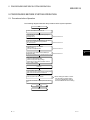
About Manuals
The following are manuals related to this product.
Request for the manuals as needed according to the chart below.
Related Manuals
Manual Name
Manual Number
PROFIBUS-DP Master Module User's Manual
Describes the overview, system configuration, specifications, functions, procedures before system
operation, programming and dedicated instructions of the QJ71PB92V.
SH-080572ENG
(13JR84)
(Sold separately)
PROFIBUS-DP Interface Module User's Manual
Describes the overview, system configuration, specifications, functions, procedures before system
operation, programming and dedicated instructions of the QJ71PB92D.
SH-080127
(13JR22)
(Sold separately)
Type AJ71PB92D/A1SJ71PB92D PROFIBUS-DP Interface Module User's Manual
Describes the overview, system configuration, specifications, functions, procedures before system
operation and programming of the A1SJ71PB92D/AJ71PB92D.
IB-66773
(13JL20)
(Sold separately)
GX Configurator-DP Version 7 Operating Manual
Explains the overview, installation method, screen operations, etc. of GX Configurator-DP Version 7.
SH-080579ENG
(13JU54)
(Sold separately)
Conformation to the EMC Directive and Low Voltage Instruction
When incorporating the Mitsubishi programmable controller into other machinery or
equipment and keeping compliance with the EMC and low voltage directives, refer to
Chapter 3 "EMC Directive and Low Voltage Instruction" of the User's Manual
(hardware) supplied with your CPU module or base unit.
The CE logo is printed on the rating plate of the programmable controller, indicating
compliance with the directives.
Note that no additional measures are necessary for this product to make compliance
with the directives.
A-7
A-7
About the Generic Terms and Abbreviations
Unless otherwise specified, this manual uses the following generic terms and
abbreviations to describe the Type QJ71PB93D PROFIBUS-DP slave module.
Generic Term/Abbreviation
QJ71PB93D
QJ71PB92V
QJ71PB92D
A1SJ71PB92D
AJ71PB92D
CPU module
GX Developer
GX Configurator-DP
PROFIBUS-DP
BBLKRD
BBLKWR
A-8
Description of the abbreviation/general terms
Abbreviation for the model QJ71PB93D PROFIBUS-DP slave module.
Abbreviation for the model QJ71PB92V PROFIBUS-DP master module.
Abbreviation for the model QJ71PB92D PROFIBUS-DP interface module.
Abbreviation for the model A1SJ71PB92D PROFIBUS-DP interface module.
Abbreviation for the model AJ71PB92D PROFIBUS-DP interface module.
Generic term for Q00JCPU, Q00CPU, Q01CPU, Q02CPU, Q02HCPU, Q06HCPU,
Q12HCPU, Q25HCPU, Q12PHCPU, Q25PHCPU, Q02UCPU, Q03UDCPU,
Q04UDHCPU and Q06UDHCPU modules.
Generic product name for SWnD5C-GPPW-E, SWnD5C-GPPW-EA, SWnD5CGPPW-EV, and SWnD5C-GPPW-EVA. ("n" means version 4 or later.)
"-A" and "-V" mean "volume license product" and "version-upgrade product"
respectively.
Generic term for the product name SWnD5C-PROFID-E. ("n" means version 5 or
later.)
Abbreviation of PROFIBUS-DP network.
Abbreviation for G.BBLKRD.
Abbreviation for G.BBLKWR.
A-8
Meanings and Definitions of the Terms
The terms used in this manual have the following meanings and definitions.
Term
PROFIBUS-DPV0
PROFIBUS-DPV1
PROFIBUS-DPV2
Class 1 master station
Class 2 master station
Slave station
Repeater
Bus terminator
Configuration tool
GSD file
Station number
Slave parameter
I/O configuration information
(Data module)
Input data
Output data
Global control
Communication watchdog
timer
Extended diagnostic error
information
Bus cycle time
Module watchdog timer
A-9
Definition
A basic version of PROFIBUS-DP.
The following functions are executable:
• I/O data exchange
• Diagnostic information notification
etc.
A PROFIBUS-DP version for which the following functions have been added to the
basic functionality of PROFIBUS-DPV0.
• Acyclic communication
• Alarm function
etc.
A PROFIBUS-DP version for which the following functions have been added to the
PROFIBUS-DPV1 functionality.
• Time stamping
etc.
A device exchanging I/O data with a slave stations. (QJ71PB92V, QJ71PB92D, etc.)
A device that communicates with slave stations and checks their station number
settings and/or operation states.
The Class 2 master station is used as a master station for supervising the network,
which can start, maintain, and diagnose the system.
A device that exchanges I/O data with a Class 1 master station. (QJ71PB93D,
ST1H-PB, etc.)
A device used to connect different segments of PROFIBUS-DP.
A terminating resistor that is connected to either end of each segment on
PROFIBUS-DP.
Software used to set slave parameters, etc. and to write them to a master station.
(GX Configurator-DP, etc.)
An electronic file that contains parameters of a slave station.
The GSD file is used to set up the slave parameters on configuration tool.
The numbers assigned to a master station and slave stations.
The station number is set within the range from 0 to 125.
The parameter for a slave station, which is set on the master station.
The setting items are described on the GSD File.
Information on I/O configuration of a slave station.
Data sent by the QJ71PB93D and received by the master station. (data input by the
master station.)
Data sent by the master station and received by the QJ71PB93D. (data output by the
master station.)
This function enables synchronization command transmission for I/O data from a
Class 1 master station to slave stations.
Watchdog timer set in the slave parameter of the master station.
Diagnostic information specific to each slave station.
Each of slave stations notifies of it to the master station when an error is detected.
PROFIBUS-DP processing time for the master station to perform cyclic transfer with
each slave station.
Watchdog timer in the QJ71PB93D.
A-9
Product Configuration
The product configuration of this product is given in the table below.
Model
QJ71PB93D
A - 10
Product name
QJ71PB93D PROFIBUS-DP slave module.
Quantity
1
A - 10
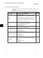
1 OVERVIEW
MELSEC-Q
1 OVERVIEW
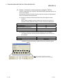
This is the user's manual for the QJ71PB93D PROFIBUS-DP slave module (hereafter
abbreviated as "QJ71PB93D"), which is used to connect a MELSEC-Q series
programmable controller to a PROFIBUS-DP network.
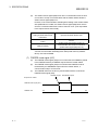
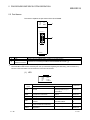
The QJ71PB93D operates as a slave station in the PROFIBUS-DP network.
Class 1 master station
(QJ71PB92V)
Slave station (QJ71PB93D)
Slave station (MELSEC-ST system)
S T 1P S D
Bus terminator
S T 1 H -P B
R UN
SYS
A U .X
ERR
Slave station
S T1PD D
R UN
11
ER R
21
R UN
11
ER R
R UN
ERR
R UN
ER R
R UN
ER R
21
AU X
RELEASE
R ESET
PR OF IBU S I/F
Bus terminator
1-1
1-1
1
1 OVERVIEW
MELSEC-Q
1.1 QJ71PB93D Features
1
(1) Conformance with EN50170 Volume 2 (Part 1, 2, 3, 4, 8)
The module conforms with EN50170 Volume 2 (Part 1, 2, 3, 4, 8) and can
communicate with the master station as a PROFIBUS-DP slave station.
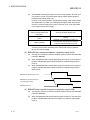
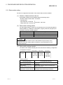
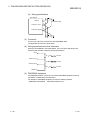
(2) I/O data communication with class 1 master station
The module can communicate I/O data with the class 1 master station (master
station that makes data communication cyclically with a slave station) of
PROFIBUS-DP.
The QJ71PB93D supports the PROFIBUS-DPV0 function.
PROFIBUS-DPV1 and PROFIBUS-DPV2, which are extended versions of
PROFIBUS-DP, are not supported.
(a) Available data size
The QJ71PB93D can handle the following size of data. (Refer to Section
4.1.1)
Input data
: Max. 122 words
Max. 192 words in total
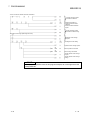
Output data : Max. 122 words
Class 1 master station
Output
image
Input
image
Bus terminator
PROFIBUS-DP network
Bus terminator
Buffer memory
Read 1
Write 2
CPU module
Output
receive
area
Output
image
Input
send
area
Input
image
QJ71PB93D (slave station)
1: Reads with BBLKRD/MOV/FROM instruction
or automatic refresh
2: Writes with BBLKWR/MOV/TO instruction or
automatic refresh
(3) Communication can be made by merely setting the master station
parameters
After you have set the parameters at the master station, the QJ71PB93D can
make communication by merely setting the station number. (Refer to Section 5.1)
1-2
1-2
1 OVERVIEW
MELSEC-Q
(4) Swapping of I/O data
When I/O data is sent/received from/to the master station, their upper and lower
bytes can be swapped.
Though PROFIBUS-DP handles the upper and lower bytes of I/O data differently
depending on the master station type, the I/O data need not be swapped in a
sequence program. (Refer to Section 4.1.4)
(5) Start/stop of refreshing the input send area
Refreshing of send data from the QJ71PB93D to the master station is
controllable by an output signal (Y00).
Providing an interlock disables the buffer memory data from being sent to the
master station at error occurrence. (Refer to Section 4.1.1)
(6) Extended trouble notification function
Data stored in the extended trouble information area of the buffer memory can be
sent to the master station as extended trouble information when the host is
faulty, for example.
When the host is not faulty anymore, notify the master station that there is no
fault. (Refer to Section 3.4.2(9))
: Diagnostics Information (device-related trouble information set by the user as
desired)
(7) Compatibility with global control function
Compatibility with the global control function allows the updating of I/O data at the
QJ71PB93D to be controlled from the class 1 master station using the command
(SYNC, UNSYNC, FREEZE, UNFREEZE) sent by the class 1 master. (Refer to
Section 4.1.3)
(8) Communication with class 2 master station
The following communications can be made with the class 2 master station
(master station designed for network management to perform booting,
maintenance and diagnostics) of PROFIBUS-DP.
• Read from input send area/output receive area
• Read of I/O configuration information
• Station number change
For the way to use each function, refer to the manual of the class 2 master
station used.
(9) I/O data separation prevention
For data transmission between the CPU module and buffer memory of
QJ71PB93D, automatic refresh or dedicated instruction are used to prevent I/O
data from being separated . (Refer to Section 4.1.2)
: The data of specified sizes are not matched with each other.
(10) Compatibility with multiple CPU system
Even when a plurality of CPU modules are installed through the multiple CPU
system, this model can be controlled by any CPU module.
1-3
1-3
2 SYSTEM CONFIGURATION
MELSEC-Q
2 SYSTEM CONFIGURATION
2.1 Applicable Systems
This section describes applicable systems.
2
(1) Mountable modules, No. of mountable modules, and mountable
base unit
(a) When mounting to CPU module
The following shows the mountable CPU modules, No. of mountable
modules, and mountable base unit of the QJ71PB93D.
Power shortage may occur depending on the combination with other
mounted modules or the number of mounted modules.
When mounting modules, pay attention to the power supply capacity.
When the power shortage occurs, review the combination of modules to be
mounted.
Mountable CPU module
CPU type
Basic model
QCPU
CPU model name
Q00JCPU
Q00CPU
Q01CPU
No. of mountable
modules 1
Mountable base unit 2
Main base unit
Extension base unit
Up to 8
Up to 24
Q02CPU
Q02HCPU
High Performance
Q06HCPU
model QCPU
Q12HCPU
Programmable
controller CPU
Up to 64
Q25HCPU
Process CPU
Redundant CPU
Q12PHCPU
Q25PHCPU
Q12PRHCPU
Q25PRHCPU
Q02UCPU
Universal model
QCPU
Up to 64
Not mountable
Up to 36
*3
*3
Q03UDCPU
Q04UDHCPU
Up to 64
Q06UDHCPU
: Mountable, : Not mountable
1 Limited to the range of the number of I/O points in the CPU module
2 Mountable on any I/O slot of the mountable base unit.
3 GX Configurator-DP cannot be used for setting.
Set station numbers in sequence programs. (Refer to Section 7.2.)
Substitute dedicated instructions or MOV/FROM/TO instructions for
automatic refresh. (Refer to Sections 4.1.1 (1) and 7.3.)
2-1
2-1
2 SYSTEM CONFIGURATION
MELSEC-Q
POINT
(1) There are restrictions on the number of automatic refresh parameters that can
be set for CPU modules.
For details, refer to Section 5.3.1(5).
(2) To utilize the data consistency function and dedicated instruction, use a CPU
module whose first 5 digits of the serial No. is "02092" or later.
If this function is used in any other models, I/O data may be identified as invalid
values.
(b) When mounting to remote I/O station of MELSECNET/H
The QJ71PB93D cannot be mounted to remote I/O station of the
MELSECNET/H.
Mount it next to the CPU module on the MELSECNET/H remote master
station.
(2) Compatibility with a multiple CPU system
When using the QJ71PB93D in a multiple CPU system, first read the QCPU
User's Manual (Multiple CPU System).
(a) Compatible QJ71PB93D
The function version of the QJ71PB93D has been "B" from the first release
and it supports the multiple CPU system.
(3) Compatibility with online module change
The QJ71PB93D cannot be changed online.
(4) Applicable software packages
Please configure the system by combining QJ71PB93D and software package
as follows:
GX Developer
: For setting CPU module parameters and creating
sequence programs (Required)
GX Configurator-DP : For setting the QJ71PB93D station number and automatic
1
refresh parameter
1 GX Configurator-DP is required when using automatic refresh.
The station number can also be set on a sequence program. (Refer to Section 5.3)
Software Version
System
Q00J/Q00/Q01CPU
Q02/Q02H/Q06H/Q12H/Q25HCPU
Q12PH/Q25PHCPU
Q02UCPU
Q03UD/Q04UDH/Q06UDHCPU
2-2
Single CPU system
GX Developer
Version 7 or later
Multiple CPU system
Version 8 or later
Single CPU system
Version 4 or later
Multiple CPU system
Version 6 or later
Single CPU system
Multiple CPU system
Single CPU system
Multiple CPU system
Single CPU system
Multiple CPU system
GX Configurator-DP
Version 5 or later
Version 7.10L or later
Version 8.48A or later
Not available
Version 8.48A or later
Version 7.02C or later
2-2
2
2 SYSTEM CONFIGURATION
MELSEC-Q
2.2 Precautions for Configuring a System
(1) Precaution for station number setting
(a) If a station number different from the one of the currently operating station is
set during I/O data communication, the communication is suspended to
execute the setting.
It is restarted after completion of the station number setting.
(b) Do not change the operation mode during execution of the station number
setting.
Doing so may disable proper station number setting or mode change.
(2) Precaution for parameter writing
(a) If a parameter based on a station number setting different from the one of the
currently operating station is written to the QJ71PB93D that is exchanging I/O
data, the I/O data communication is suspended. It is restarted after
completion of parameter writing.
(b) Do not change the operation mode from the sequence program during
parameter writing.
Doing so may disable proper station number setting or mode change.
(c) Do not write parameters from multiple GX Configurator-DPs to a single
QJ71PB93D at the same time.
Doing so makes the parameter values of the QJ71PB93D incorrect.
(3) When switching the operation mode using Y11/X11 on the
sequence program
Be sure to switch the mode while the module READY signal (X1D) of the
QJ71PB93D is ON.
If data are read from or written to the buffer memory with the X1D status ignored,
the CPU module may detect an error to stop the sequence calculation.
2-3
2-3
2 SYSTEM CONFIGURATION
MELSEC-Q
2.3 Confirmation of Function Version and Serial No.
This section explains how to check the function version and serial No. of the
QJ71PB93D.
(1) Checking the "Rating plate" on the side of the module
The serial No. and function version of the module are printed in the SERIAL
section of the rating plate.
Serial No. (Upper 5 digits)
Function version
Conformed standard
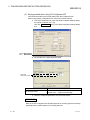
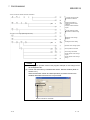
(2) Checking through GX Developer
The following explains how to check the serial No. and function version of the
module through GX Developer.
The serial No. and function version are displayed on the "Product information list"
or "Module's Detailed Information" screen of GX Developer.
The procedure for checking the serial No. and function version on the "Product
information list" screen is shown below.
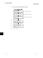
[Start Procedure]
"Diagnosis"
"System monitor"
"Product inf. list"
[Serial No., Ver., Product No.]
The serial No. of the module is displayed in the "Serial No." column.
The function version of the module is displayed in the "Ver." column.
The serial No. (Product No.) shown on the rating plate is displayed in the
*1
"Product No." column.
Note that "-" is displayed in the "Product No." column for the QJ71PB93D
since this module is not supporting Product No. display.
2-4
2-4
2 SYSTEM CONFIGURATION
MELSEC-Q
1 The Product No. is displayed in the column only when the Universal model QCPU
is used.
POINT
The serial No. described on the rated plate may not match with the serial No.
displayed on the product information of GX Developer.
The serial No. on the rated plate describes the management information of the
product.
The serial No. displayed on the product information of GX Developer describes
the function information of the product.
The function information of the product is updated when adding functions.
2-5
2-5
3 SPECIFICATIONS
MELSEC-Q
3 SPECIFICATIONS
This chapter describes the performance specifications, network configuration, I/O
signals, buffer memory and operation modes of the QJ71PB93D.
For the general specifications of the QJ71PB93D, refer to the QCPU User's Manual
(Hardware Design, Maintenance and Inspection).
3.1 Performance Specifications
Item
Specifications
Slave station (Complies with EN50170 Volume2 (Part 1, 2, 3, 4, 8))
Station numbers that may be set
0 to 125
Max. number of data that may be
communicated
Number of I/O data is 192 words in total. (Size of I/O data is up to 122 words.)
Transmission specifications
PROFIBUS-DP station type
Electrical standard/characteristics
Complies with EIA-RS485
Medium
Shielded twisted pair cable (Type A) (Refer to Section 5.7.1)
Network topology
Bus topology (Tree topology when repeaters are used)
Data link method
Polling method
Encoding method
3
2
NRZ
Transmission speed
1
9.6 kbps to 12 Mbps (Refer to (1) in this section)
Transmission distance
Differs depending on the transmission speed (Refer to (1) in this section)
Maximum number of repeaters
3 units (Refer to (1) in this section)
Number of connectable modules
(Per segment)
32 units (including repeaters)
Flash ROM write count
Max. 10000 times
Number of occupied I/O points
32 points (I/O assignment : 32 intelligent points)
5VDC Internal power consumption
0.44 A
External dimensions
98(3.86) (H) × 27.4(1.08) (W) × 90(3.55) (D) [mm(inch)]
Weight
0.11 kg
1 Transmission speed control within +/- 0.3% (EN50170 Volume 2 compliant)
2 Factory-set to "126" (EN50170 Volume 2 compliant)
Set a station number within 0 to 125 for I/O data communication.
For the noise immunity, withstand voltage, insulation resistance and others in the
programmable controller system using this module, refer to the power supply module
specifications given in the QCPU User's Manual (Hardware Design, Maintenance and
Inspection).
(1) Transmission distance
Transmission Speed
Transmission Distance
Max. Transmission Distance when
Repeater is Used 3
9.6 kbps
1200 m (3937 ft.)/segment
4800 m (15748 ft.)/network
187.5 kbps
1000 m (3281 ft.)/segment
4000 m (13123 ft.)/network
500 kbps
400 m (1312 ft.)/segment
1600 m (5249 ft.)/network
1.5 Mbps
200 m (656 ft.)/segment
800 m (2625 ft.)/network
100 m (328 ft.)/segment
400 m (1312 ft.)/network
19.2 kbps
93.75 kbps
3 Mbps
6 Mbps
12 Mbps
3 The max. transmission distance in the table above is based on the case where 3 repeaters are used.
The calculation formula for the transmission distance extended using a repeater(s) is:
Max. transmission distance [m/network] = (Number of repeaters + 1) x Transmission distance [m/segment]
3-1
3-1
3 SPECIFICATIONS
MELSEC-Q
3.2 Network Configuration
This section explains the basic PROFIBUS-DP configuration for using the QJ71PB93D
as a slave station.
(1) System equipment
The following table shows the equipment required for the PROFIBUS-DP system.
System Equipment
Slave station
3
Description
QJ71PB93D
Class 1 master station
QJ71PB92V, QJ71PB92D, etc.
Configuration tool
Configurator applicable to the master station
Repeater
Required when 32 or more slave stations are connected
PROFIBUS cable
Refer to section 5.7.1
Bus terminator
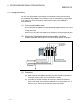
(2) Network configuration
In the PROFIBUS-DP system configuration, the following conditions must be
satisfied:
(a) Number of connectable modules in the whole network (when repeaters are
used)
Master station + Slave station 1 126
1: Including the QJ71PB93D
(b)
Number of connectable modules per segment
Master station + Slave station 1 + repeaters 2
1: Including the QJ71PB93D
2: A repeater is counted for both segments.
32
(c)
Maximum number of repeaters
Up to 3 repeaters can be used for communication between master station
and the QJ71PB93D.
(d)
Number of slave stations that are connectable to master station
The maximum number of slave stations that may be connected to one
master station depends on the specifications of the master station.
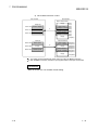
Class 1
Master station
Bus terminator
Bus terminator
QJ71
CPU
module PB93D
Slave
Station No. 1
Slave
Station No. 2
Slave
Station No. 30
Bus terminator
Repeater
Bus terminator
QJ71
CPU
module PB93D
Slave
Station No. 31
3-2
Slave
Station No. 32
Slave
Station No. 60
3-2
3 SPECIFICATIONS
MELSEC-Q
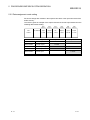
3.3 I/O Signal
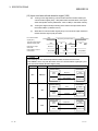
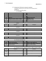
3.3.1 I/O signal list
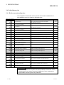
The I/O signal configuration used in the QJ71PB93D and the data communications
with the CPU module are described below.
The following I/O signal assignment is based on the case where the start I/O No. of the
QJ71PB93D is "0000" (installed to slot 0 of the main base unit).
Device X represents an input signal from the QJ71PB93D to the CPU module.
Device Y shows an output signal from the CPU module to the QJ71PB93D.
Refer to the corresponding reference sections for details.
Signal direction: QJ71PB93D
Device No.
CPU module
Description
Signal direction: CPU module
Device No.
QJ71PB93D
Description
X00
Watchdog timer error
Y00
Input send area refresh directive signal
X01
I/O communication signal
Y01
Use prohibited
X02
Extension trouble notification completion signal
Y02
Extension trouble notification request signal
X03
Module error signal
Y03
Module error reset request signal
X04
Use prohibited
Y04
X05
SYNC mode signal
Y05
X06
SYNC receive signal
Y06
X07
FREEZE mode signal
Y07
X08
X09
Use prohibited
Y08
Use prohibited
Y09
X0A
BBLKRD start request acceptance completion signal
Y0A
BBLKRD start request signal
X0B
BBLKWR start request acceptance completion signal
Y0B
BBLKWR start request signal
X0C
Y0C
X0D
X0E
Y0D
Use prohibited
Y0E
X0F
Use prohibited
Y0F
X10
Y10
X11
Operation mode change completion signal
Y11
Operation mode change request signal
X12
Use prohibited
Y12
Use prohibited
X13
Station number change completion signal
Y13
Station number change request signal
X14
Y14
X15
Y15
X16
Y16
X17
X18
Y17
Use prohibited
Y18
X19
Y19
X1A
Y1A
X1B
Y1B
X1C
Y1C
X1D
X1E
X1F
Module READY signal
Use prohibited
Y1D
Y1E
Use prohibited
Y1F
POINT
Do not output (turn ON) the "Use prohibited" signals.
Doing so may cause the programmable controller system malfunction.
3-3
3-3
3 SPECIFICATIONS
MELSEC-Q
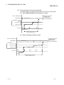
3.3.2 I/O signal detail description
(1) Watchdog timer error (X00)
(a)
This signal turns on when a watchdog timer error occurs on the
QJ71PB93D.
(b)
The watchdog timer error (X00) does not turn off until the following
operation is performed.
• Turning the programmable controller power OFF to ON
• Resetting the CPU module
If the signal turns on again, a hardware error may be the cause.
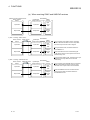
(2) I/O communication signal (X01)
(a)
This signal turns on when the module is ready to communicate with the
master station properly.
(b)
While the I/O communication signal (X01) is on, the output receive area is
updated to the output data sent from the master station.
(It is independent of the status of the input send area refresh directive
signal (Y00).)
(c)
The I/O communication signal (X01) turns off when a communication timeout error occurs due to a stop of communication with the master station.
However, if the communication watchdog timer setting in the master station
side parameters is "invalid", the I/O communication signal does not turn off
since a communication time-out error does not occur.
(The output data in the output receive area is held.)
Communication watchdog timer Setting
in Master Station Side Parameters
Operation at Master Station Fault
No error
Invalid
(I/O communication signal (X01) remains on)
Communication time-out error occurrence
Valid (2 to 65025)
(I/O communication signal (X01) turns off)
The communication watchdog timer setting can be confirmed in the
"Current communication watchdog timer value (buffer memory address:
8D1H)" of the QJ71PB93D.
(d)
Use this signal as a signal for interlocking output receive area read
performed with the MOV/FROM instruction.
Communication with
master station
Communication stop
I/O communication signal (X01)
Data update in output
receive area
Output receive area
(Buffer memory address :
0H to BFH)
3-4
OFF
Not updated
Communication in progress
ON
Updated
Communication stop
OFF
Not updated
MOV/FROM instruction
Execution of read from
output receive area
3-4
3 SPECIFICATIONS
MELSEC-Q
(3) Extension trouble notification completion signal (X02)
(a)
The extension trouble notification completion signal (X02) turns on when
the extension trouble information is sent to the master station by turning on
the extension trouble notification request signal (Y02).
(While the I/O communication signal (X01) is off, the extension trouble
notification completion signal (X02) does not turn on since an extension
trouble notification request is ignored.)
(b)
Turning off the extension trouble notification request signal (Y02) turns off
the extension trouble notification completion signal (X02).
I/O communication signal (X01)
Extension trouble
notification request
Extension trouble notification
request signal (Y02)
Extension trouble
notification completion
Extension trouble notification
completion signal (X02)
Extension trouble information area
(Buffer memory address :
7f9H to 805H)
MOV/TO
Instruction
Extension trouble
information write
POINT
When performing the extension trouble notification requests consecutively, provide
an interlock using the extension trouble notification completion signal (X02) in the
procedure shown above.
(4) Module error signal (X03)
(a)
This signal turns on when an error occurs.
At this time, an error code is stored into the module error information area
(buffer memory address: 7F8H)).
(b)
This signal turns off when the error is reset by turning on the module error
reset request signal (Y03) or resetting the CPU, for example. At this time,
the ERR. LED goes off and the error code is cleared.
The module error reset request signal (Y03) turns off after confirming that
the module error signal (X03) have turned off.
(c)
Error reset
Module error reset request signal (Y03)
Error detection
Module error signal (X03)
MOV/FROM
instruction
Module error information area
(Buffer memory address : 7F8H)
The error code is read from the buffer memory to the CPU module.
(5) SYNC mode signal (X05)
3-5
(a)
This signal turns on when the QJ71PB93D is placed in the SYNC mode by
a SYNC request from the master station.
(b)
The SYNC mode signal (X05) turns off when the SYNC mode is terminated
by an UNSYNC request from the master station, a communication stop or a
CPU reset.
3-5
3 SPECIFICATIONS
MELSEC-Q
(c)
The SYNC LED turns on/off in synchronization with the on/off of the SYNC
mode signal (X05).
(d)
The SYNC mode signal (X05) turns off if a communication time-out error
occurs due to a stop of communication with the master station while the
SYNC mode signal (X05) is on.
However, if the communication watchdog timer setting in the master station
side parameters is "invalid", the SYNC mode signal (X05) does not turn off
since a communication time-out error does not occur. (The output data in
the output receive area is held.)
Communication watchdog timer
Setting in Master Station Side
Operation at Master Station Fault
Parameters
No error
Invalid
(SYNC mode signal (X05) remains on)
Communication time-out error occurrence
Valid (2 to 65025)
(SYNC mode signal (X05) turns off)
The communication watchdog timer setting can be confirmed in the
"Current communication watchdog timer value (buffer memory address:
8D1H)" of the QJ71PB93D.
(6) SYNC receive signal (X06)
(a)
The SYNC receive signal (X06) turns on receipt of a SYNC request from
the master station.
(b)
While the SYNC mode signal (X05) is on, the receipt of a SYNC request
from the master station changes the on/off state of the SYNC receive signal
(X06).
At this time, the SYNC mode signal (X05) remains on.
(c)
The SYNC receive signal (X06) turns off when the SYNC mode is
terminated by an UNSYNC request from the master station, a
communication stop or a CPU reset.
SYNC request
SYNC request
SYNC request
UNSYNC request
Request from master
SYNC mode signal (X05)
SYNC receive signal (X06)
SYNC LED
3-6
Off
On
Off
3-6
3 SPECIFICATIONS
MELSEC-Q
(d)
The SYNC receive signal (X06) turns off if a communication time-out error
occurs due to a stop of communication with the master station while the
SYNC receive signal (X06) is on.
However, if the communication watchdog timer setting in the master station
side parameters is "invalid", the SYNC receive signal (X06) does not turn
off since a communication time-out error does not occur. (The output data
in the output receive area is held.)
Communication watchdog timer
Operation at Master Station Fault
Setting in Master Station Side
Parameters
No error
Invalid
(SYNC receive signal (X06) remains on)
Communication time-out error occurrence
Valid (2 to 65025)
(SYNC receive signal (X06) turns off)
The communication watchdog timer setting can be confirmed in the
"Current communication watchdog timer value (buffer memory address:
8D1H)" of the QJ71PB93D.
(7) FREEZE mode signal (X07)
(a)
The FREEZE mode signal (X07) turns on when the QJ71PB93D is placed
in the FREEZE mode by a FREEZE request from the master station.
(b)
The FREEZE mode signal (X07) turns off when the FREEZE mode is
terminated by an UNFREEZE request from the master station, a
communication stop or a CPU reset.
(c)
The FREEZE LED turns on/off in synchronization with the on/off of the
FREEZE mode signal (X07).
FREEZE request
UNFREEZE request
Request from master
FREEZE mode signal (X07)
FREEZE LED
3-7
Off
On
Off
3-7
3 SPECIFICATIONS
MELSEC-Q
(d)
The FREEZE mode signal (X07) turns off if a communication time-out error
occurs due to a stop of communication with the master station while the
FREEZE mode signal (X07) is on.
However, if the communication watchdog timer setting in the master station
side parameters is "invalid", the FREEZE mode signal (X07) does not turn
off since a communication time-out error does not occur. (The output data
in the output receive area is held.)
Communication watchdog timer
Setting in Master Station Side
Operation at Master Station Fault
Parameters
Invalid
Valid (2 to 65025)
No error
(FREEZE mode signal (X07) remains on)
Communication time-out error occurrence
(FREEZE mode signal (X07) turns off)
The communication watchdog timer setting can be confirmed in the
"Current communication watchdog timer value (buffer memory address:
8D1H)" of the QJ71PB93D.
(8) BBLKRD start request acceptance completion signal (X0A)
(a)
This signal is used as an interlock condition signal to execute the dedicated
instruction BBLKRD.
(b)
When the BBLKRD start request signal (Y0A) is turned on in the sequence
program, the BBLKRD start request acceptance completion signal (X0A)
turns on.
(c)
When the BBLKRD start request signal (Y0A) is turned off in the sequence
program, the BBLKRD start request acceptance completion signal (X0A)
also turns off.
BBLKRD start request signal (Y0A)
BBLKRD start request acceptance
completion signal (X0A)
BBLKRD instruction
(9) BBLKWR start request acceptance completion signal (X0B)
3-8
(a)
This signal is used as an interlock condition signal to execute the dedicated
instruction BBLKWR.
(b)
When the BBLKWR start request signal (Y0B) is turned on in the sequence
program, the BBLKWR start request acceptance completion signal (X0B)
turns on.
3-8
3 SPECIFICATIONS
MELSEC-Q
(c)
When the BBLKWR start request signal (Y0B) is turned off in the sequence
program, the BBLKWR start request acceptance completion signal (X0B)
also turns off.
BBLKWR start request signal (Y0B)
BBLKWR start request acceptance
completion signal (X0B)
BBLKWR instruction
(10) Operation mode change completion signal (X11)
(a)
This signal turns on when an operation mode change is completed by
setting the required operation mode to the operation mode change request
area (buffer memory address: 8CFH) and turning on the operation mode
change request signal (Y11).
At this time, the result is stored into the operation mode change result area
(buffer memory address: 8D0H).
(b)
Turning off the operation mode change request signal (Y11) after
confirmation of the result turns off the operation mode change completion
signal (X11).
(c)
This signal turns on at either normal or abnormal completion of an
operation mode change.
At abnormal completion, the operation mode change request is made
invalid and operation continues in the operation mode that had been used
before the change request was given.
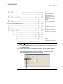
Input send area refresh
directive signal (Y00)
Operation mode change
request signal (Y11)
Operation mode change
completion signal (X11)
Operation mode change result area
(Buffer memory address: 2256(8D0H))
Change result of operation mode
MOV/TO
instruction
Sets the operation mode
in "operation mode change
request area (Address : 8CFH)".
3-9
MOV/FROM
instruction
Checks result in "operation mode
change result area (Address : 8D0H)"
and "current operation mode
(Address : 8CEH)".
3-9
3 SPECIFICATIONS
MELSEC-Q
(11) Station number change completion signal (X13)
(a)
This signal turns on when the station number setting is completed by
setting the station number to the station number change request area
(buffer memory address: 203H) and turning on the station number change
request signal (Y13).
(b)
Check the setting result in the operation station number area (buffer
memory address: 201H) and module error information area (buffer memory
address: 7F8H) of the buffer memory.
(c)
Turning off the station number change request signal (Y13) after
confirmation of the result turns off the station number change completion
signal (X13).
(d)
If a station number error (error code: 1002H) has occurred, the station
number change request is made invalid and operation continues with the
station number that had been used before the change request was given.
(e)
Turning on the station number change request signal (Y13) suspends I/O
communication.
Turning on the station number change completion signal (X13) resumes I/O
communication.
Input send area refresh
directive signal (Y00)
Station number change
request signal (Y13)
Station number change
completion signal (X13)
Buffer memory
MOV/TO
instruction
Sets station number in "station
number change request area
(Address : 203H)".
MOV/FROM
instruction
Checks result in "operation station
number area (Address : 201H),
module error information area
(Address : 7F8H)".
(12) Module READY signal (X1D)
3 - 10
(a)
This signal turns on when the QJ71PB93D is enabled for access from the
CPU module. (It turns on regardless of the operation mode.)
(b)
This signal turns off when the QJ71PB93D is disabled for access from the
CPU module due to a module watchdog timer error, hardware fault or like.
3 - 10
3 SPECIFICATIONS
MELSEC-Q
(13) Input send area refresh directive signal (Y00)
(a)
Turning on this signal during communication with the master station (I/O
communication signal (X01) = ON) starts data communication of the input
send area (buffer memory addresses: 100H to 1BFH) in the buffer memory.
(b)
Turning this signal off stops sending of the data in the input send area to
the master station. (0 data are sent.)
(c)
While the I/O communication signal (X01) is off, ON of the input send area
refresh directive signal (Y00) is invalid.
OFF
(communication stop)
I/O communication
signal (X01)
Input send area refresh
directive signal (Y00)
ON (during communication)
OFF
ON
Data send in input
send area
Not sent
Sent
Data update in output
receive area
Not updated
OFF
OFF
(communication stop)
OFF
ON
Not sent
Updated
Not updated
POINT
The following are the relationships between data send and receive of the
QJ71PB93D, which vary with the states of the I/O communication signal (X01) and
input send area refresh directive signal (Y00).
X01 State
Y00 State
Data in Output Receive Area/Input Send Area
Master station
OFF
ON/OFF
Input
area
Output
area
QJ71PB93D
Not sent
Not updated
Master station
ON
Input
area
Output
area
Input
send area
Output
receive area
QJ71PB93D
Sent
Updated
Input
send area
Output
receive area
ON
Master station
OFF
Input
area
Output
area
3 - 11
QJ71PB93D
0 data sent
Updated
Input
send area
Output
receive area
3 - 11
3 SPECIFICATIONS
MELSEC-Q
(14) Extension trouble notification request signal (Y02)
(a)
Turning on the extension trouble notification request signal (Y02) sends the
data set in the extension trouble information area (buffer memory address:
7F9H to 805H) to the master station as extension trouble information. (The
extension trouble notification request is ignored while the I/O
communication signal (X01) is off.)
(b)
When you have checked that the extension trouble notification completion
signal (X02) is on, turn off the extension trouble notification request signal
(Y02).
(c)
Refer to (3) in this section for the on/off timing.
POINT
To turn on/off Y02, provide an interlock using X02.
(15) Module error reset request signal (Y03)
(a)
Turning on the module error reset request signal (Y03) resets the error of
the QJ71PB93D. (The module error signal (X03) turns off and the ERR.
LED goes off.)
(b)
When you have checked that the module error signal (X03) is off, turn off
the module error reset request signal (Y03).
(c)
Making an error reset clears the error code in the module error information
area (buffer memory address: 7F8H).
(d)
Refer to (4) in this section for the on/off timing.
(16) BBLKRD start request signal (Y0A)
3 - 12
(a)
This signal is used to start the processing of the dedicated instruction
BBLKRD.
When executing the dedicated instruction BBLKRD, always turn on the
BBLKRD start request signal (Y0A) to turn on the BBLKRD start request
acceptance completion signal (X0A) so that it is used as an interlock
condition.
(b)
When the BBLKRD start request signal (Y0A) is turned on in the sequence
program, the QJ71PB93D starts the processing of the dedicated instruction
BBLKRD.
(c)
When the BBLKRD start request signal (Y0A) is turned off from the
sequence program, the processing of the dedicated instruction BBLKRD is
ignored.
(d)
Only when using the dedicated instruction BBLKRD, turn on the BBLKRD
start request signal (Y0A).
Note that, if the dedicated instruction BBLKRD is not executed after the
BBLKRD start request signal (Y0A) has been turned on, the transmission
delay time between the master and a slave stations is prolonged.
3 - 12
3 SPECIFICATIONS
MELSEC-Q
(17) BBLKWR start request signal (Y0B)
(a)
This signal is used to start the processing of the dedicated instruction
BBLKWR.
When executing the dedicated instruction BBLKRD, always turn on the
BBLKRD start request signal (Y0B) to turn on the BBLKRD start request
acceptance completion signal (X0B) so that it is used as an interlock
condition.
(b)
When the BBLKWR start request signal (Y0B) is turned on in the sequence
program, the QJ71PB93D starts the processing of the dedicated instruction
BBLKWR.
(c)
When the BBLKWR start request signal (Y0B) is turned off from the
sequence program, the processing of the dedicated instruction BBLKWR is
ignored.
(d)
Only when using the dedicated instruction BBLKWR, turn on the BBLKWR
start request signal (Y0B).
Note that, if the dedicated instruction BBLKWR is not executed after the
BBLKWR start request signal (Y0B) has been turned on, the transmission
delay time between the master and a slave stations is prolonged.
(18) Operation mode change request signal (Y11)
(a)
Turn on the operation mode change request signal (Y11) when changing
the operation mode to the one set in the operation mode change request
area (buffer memory address: 8CFH).
(b)
When you have checked that the operation mode change completion signal
(X11) is on, turn off the operation mode change request signal (Y11).
(c)
Refer to (10) in this section for the on/off timing.
(19) Station number change request signal (Y13)
(a)
Turn on the station number change request signal (Y13) when changing the
station number to the one set in the station number change request area
(buffer memory address: 203H).
(b)
When you have checked that the station number change completion signal
(X13) is on, turn off the station number change request signal (Y13).
(c)
Refer to (11) in this section for the on/off timing.
POINT
Station numbers can be set from the class 2 master station.
In this case, specifying "TRUE" for "No_Add_Chg" disables the station number
change on the QJ71PB93D.
The station number of the QJ71PB93D cannot be changed while the station
number change is disabled.
To change the station number again, clear the station number in the station number
change request area of the QJ71PB93D (buffer memory address: 515(203H)) to
cancel the disabled status. (Refer to Section 3.4.2 (6))
3 - 13
3 - 13
3 SPECIFICATIONS
MELSEC-Q
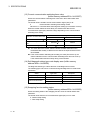
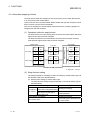
3.4 Buffer Memory List
3.4.1 Buffer memory/configuration
The configuration of the buffer memory used to receive and send data with the
QJ71PB93D and the CPU module is described below.
Buffer memory address
Hexadecimal decimal
0H
0
BFH
191
C0H 192
FFH 255
100H 256
1BFH 447
1C0H 448
1FFH 511
Area name
Output receive area
System area (Use prohibited)
Input send area
System area (Use prohibited)
Description
Stores the output data received from the master station.
(Max. usable range 122 words)
⎯
Used to set the input data to be sent to the master station.
(Max. usable range 122 words)
⎯
Read/Write
Read
⎯
Read/Write
⎯
200H 512
Operation baud rate
Stores the baud rate in current operation.
Read
201H 513
Operation station number
Stores the station number in current operation.
Read
202H 514
Station number set on flash ROM
Stores the station number saved on the flash ROM.
Read
203H 515
Station number change request area
Used to set a new station number to be set in response to the station
number change request signal (Y13).
204H 516
Station number rewritable count to flash ROM
Stores the remaining number of times when the station number can be
saved onto the flash ROM during continuous operation.
Read
⎯
⎯
205H 517
7F7H 2039
7F8H 2040
7F9H 2041
805H 2053
806H 2054
8CDH 2253
8CEH 2254
System area (Use prohibited)
Module error information
Stores the error code detected by the QJ71PB93D.
Extension trouble information area
Used to set the extension trouble notification data to the master
station.
System area (Use prohibited)
⎯
Read/Write
Read
Read/Write
⎯
Current operation mode
Stores the operation mode in current operation.
8CFH 2255
Operation mode change request area
Used to set a new operation mode to be set in response to the
operation mode change request signal (Y11).
8D0H 2256
Operation mode change result
Stores the result of changing the operation mode in response to the
operation mode change request signal (Y11).
8D1H 2257
Current communication watchdog timer value
Stores the communication watchdog timer value in current operation.
Read
8D2H 2258
Self-diagnostic status type code display area
Stores the diagnostic status type code at the time of self-diagnostics.
Read
8D3H 2259
Swapping function setting status
Stores the setting status of the swapping function in current operation.
Read
⎯
⎯
8D4H 2260
8DFH 2271
8E0H 2272
8EBH 2283
8ECH 2284
8EFH 2287
8F0H 2288
8FBH 2299
8FCH 2300
AFFH 2815
System area (Use prohibited)
Output receive area used status
System area (Use prohibited)
Input send area used status
System area (Use prohibited)
Stores the current used status of the output receive area.
⎯
Stores the current used status of the input send area.
⎯
Read
Read/Write
Read
Read
⎯
Read
⎯
POINT
Do not write any data in the "system area (Use prohibited)" of the buffer memory.
If data is written to the "system area (Use prohibited)" , there is a risk that the
programmable controller system may malfunction.
3 - 14
3 - 14
3 SPECIFICATIONS
MELSEC-Q
3.4.2 Buffer memory detail description
(1) Output receive area
(buffer memory address 0H to BFH: Un\G0 to Un\G191)
Stores the output data received from the master station.
The structure varies with the data module setting and data assignment mode
setting in the slave parameters. (Refer to Section 5.2.1 to 5.2.3)
(2) Input send area
(buffer memory address 100H to 1BFH: Un\G256 to Un\G447)
Used to store the input data to be sent to the master station.
The structure varies with the data module setting and data assignment mode
setting in the slave parameters. (Refer to Section 5.2.1 to 5.2.3)
(3) Operation baud rate (buffer memory address 200H: Un\G512)
Stores the baud rate in current operation.
Baud Rate
Stored Value
Baud rate not yet recognized
0000H
9.6 kbps
96E2H
19.2 kbps
19E3H
45.45 kbps
45E3H
93.75 kbps
93E3H
187.5 kbps
18E4H
500 kbps
05E5H
1.5 Mbps
15E5H
3 Mbps
03E6H
6 Mbps
06E6H
12 Mbps
12E6H
The stored value while the I/O communication signal (X01) is on is valid.
Use the master station parameter to set the baud rate of the PROFIBUS-DP.
(4) Operation station number (buffer memory address 201H: Un\G513)
Stores the station number of the QJ71PB93D in current operation.
The storage range is 0 to 126.
The stored value while the I/O communication signal (X01) is on is valid.
If the station number is not set (the station number is as set in the factory or has
been cleared), "126" is stored.
I/O data cannot be communicated if the station number is not set.
3 - 15
3 - 15
3 SPECIFICATIONS
MELSEC-Q
(5) Station number set on flash ROM
(buffer memory address 202H: Un\G514)
Stores the station number of the QJ71PB93D set to the flash ROM.
The storage range is 0 to 125.
If the station number is not set to the flash ROM (the station number is as set in
the factory or has been cleared), "FFFFH" is stored.
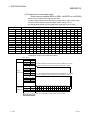
(6) Station number change request area
(buffer memory address 203H: Un\G515)
Used to set any of the following values when setting a new station number of the
QJ71PB93D in response to the station number change request signal (Y13).
Set Value
Description
Set a station number.
By turning on b8, the station number is saved onto the flash ROM.
b15 b14 b13 b12 b11 b10 b9
b8
b7
b6
b5
b4
b3
b2
b1
b0
Fixed to 0
0000H to 007DH or
0100H to 017DH
FFFFH
0: Not save onto the flash ROM
1: Save onto the flash ROM
Set a station number within the
range from 0H to 7DH (0 to125).
(Example 1) Set the station number to 12. (Not saved onto the flash
ROM): 000CH
(Example 2) Set the station number to 12. (Saved onto the flash
ROM): 010CH
Clears the station number.
After clearing, the operation station number is "126".
The station number set to the flash ROM is "FFFEH".
POINT
(1) Saving the station number to the flash ROM enables the operation based on the
station number setting stored in the flash ROM even if the module is powered
OFF and then ON or the CPU module is reset.
(2) At power-on or at CPU reset, "FFFEH" is stored.
Turn on the station number change request signal (Y13) after storing a setting
value given in the above table.
Executing the station number change request with any invalid value results in a
station number error (error code: 1002H).
(7) Station number rewritable count to flash ROM
(buffer memory address 204H: Un\G516)
Stores the remaining number of times when the station number setting can be
saved onto the flash ROM during operation.
The initial value is 60.
(a) Counting down the number of times
Every time the station number is changed on the flash ROM, the count is
decremented by 1.
The count is not decremented when station number setting is requested
with the same station number as the one saved on the flash ROM (buffer
memory address: 202H).
3 - 16
3 - 16
3 SPECIFICATIONS
MELSEC-Q
(b)
Resetting the count
The count is reset to 60 by resetting the CPU, by powering on the
QJ71PB93D or by clearing the station number on the flash ROM using the
station number change request signal (Y13).
(c)
If an attempt is made to rewrite the station number on the flash ROM at the
remaining count of 0
A station number rewrite count excess error (error code: 2001H) occurs and
the station number on the flash ROM is not changed.
If the station number rewrite count excess error has occurred, switch power
on again, reset the CPU, or clear the station number on the flash ROM
using the station number change request signal (Y13). (This returns the
remaining count to 60 times.)
(8) Module error information (buffer memory address 7F8H: Un\G2040)
Stores the error code of the error that occurred in the QJ71PB93D.
Refer to Section 9.4 for the error codes.
(9) Extension trouble information area
(buffer memory address 7F9H to 805H: Un\G2041 to Un\G2053)
Used to set the extension trouble information to be sent to the master station.
The extension trouble information sent by the QJ71PB93D is the Device Related
Diagnostic specified in PROFIBUS.
The extension trouble information can be set in a sequence program.
Data length
: Data length of the data to be sent as extension
trouble information (bytes units)
Extension trouble information : Any data to be set to the master station (max. 24
bytes)
7F9H
7FAH
805H
Data length
Extension trouble
information
The extended trouble information area is used as described below when an
extended trouble occurs and when the extended trouble is removed.
(a) When extended trouble occurs
When the host becomes faulty, for example, the data stored in the
extended trouble information area of the buffer memory is sent to the
master station as extended trouble information.
In the following procedure, the QJ71PB93D can notify the master station of
the extended trouble of the host.
1) In the buffer memory 7FAH to 805H, set the data to be sent to the
master station.
2) In the buffer memory 7F9H, set the length of the data to be sent to the
master station.
3) Turn ON the extension trouble notification request signal (Y02).
4) After the extension trouble notification completion signal (X02) has
turned ON, turn OFF the extension trouble notification request signal
(Y02).
3 - 17
3 - 17
3 SPECIFICATIONS
MELSEC-Q
(b)
When extended trouble is removed
When the host is not faulty anymore, notify the master station that there is
no fault.
In the following procedure, the QJ71PB93D can notify the master station
that the extended trouble of the host has been removed.
1) In the buffer memory 7F9H, set the data length 0.
2) Turn ON the extension trouble notification request signal (Y02).
3) After the extension trouble notification completion signal (X02) has
turned ON, turn OFF the extension trouble notification request signal
(Y02).
(c)
DIA LED of QJ71PB93D front panel is turned on as follows.
Y02
X02
Except 0
7F9H
DIA
Off
0
On
Off
(10) Current operation mode (buffer memory address 8CEH: Un\G2254)
Stores the current operation mode.
Refer to Section 3.5 for the operation mode.
Stored Value
Mode
0000H
Normal operation mode
0002H
Self-diagnostic mode
At power-on or CPU reset, the module starts in the normal operation mode.
(11) Operation mode change request area
(buffer memory address 8CFH: Un\G2255)
Set any of the following values when changing the operation mode of the
QJ71PB93D with the operation mode change request signal (Y11).
Set Value
Description
0000H
Normal operation mode
0002H
Self-diagnostic mode
At power-on or CPU reset, "FFFEH" is stored.
If an operation mode change request is executed with any value other than the
set value, the operation cannot be guaranteed.
(12) Operation mode change result area
(buffer memory address 8D0H: Un\G2256)
Stores the result of changing the operation mode in response to the operation
mode change request signal (Y11).
0 : Normal completion
1 : Abnormal completion (A change request was made with an illegal value
set in the operation mode change request area (buffer memory address:
8CFH))
3 - 18
3 - 18
3 SPECIFICATIONS
MELSEC-Q
(13) Current communication watchdog timer value
(buffer memory address 8D1H: Un\G2257)
Stores the communication watchdog timer value set in the master station side
parameters.
The stored value is invalid if the I/O communication signal (X01) is off.
0
: Communication watchdog timer setting invalid
Other than 0 : Communication watchdog timer setting (in increments of 10ms)
When the master station becomes faulty, the send/receive data and I/O
communication signal (X01) statuses change depending on the communication
watchdog timer setting.
Statuses at master station fault
Send data to master station
Current communication watchdog timer value (This area)
1
Data update in output receive
area
I/O communication signal (X01)
0
Other than 0
Retained
2
Cleared
Retained
2
Cleared
ON
2
OFF
1: The send data to the master station indicates the data that flows on the
PROFIBUS-DP actually. It differs from the data in the input send area of the
QJ71PB93D.
2: If the communication watchdog timer setting is invalid (This area is 0), the
data is retained since the communication watchdog timer does not count up
if the master station becomes faulty during communication.
(14) Self-diagnostic status type code display area (buffer memory
address 8D2H: Un\G2258)
The diagnostic status type code at the time of self-diagnostics is stored.
The following type code can be confirmed during self-diagnostics or at abnormal
termination.
Status
Type Code
Description
During self-diagnostics
0001H to 0009H
During self-diagnostics
At normal termination
0H
Normal termination
8001H to 8006H
Hardware fault
8007H
Swap test error
At abnormal termination
Refer to Section 5.6 for the way to run the self-diagnostics.
(15) Swapping function setting status
(buffer memory address 8D3H: Un\G2259)
Stores the setting status of the swapping function set in the master station side
parameter.
The stored value while the I/O communication signal (X01) is on is valid.
0 : Without swap setting
1 : With swap setting
3 - 19
3 - 19
3 SPECIFICATIONS
MELSEC-Q
(16) Output receive area used status
(buffer memory address 8E0H to 8EBH: Un\G2272 to Un\G2283)
Stores the used status of the output receive area.
The bits corresponding to the buffer memory addresses in output receive area
set by the master station parameters (Data module setting) turn on.
The stored value while the I/O communication signal (X01) is on is valid.
Buffer Memory Address
Corresponding Buffer Memory Addresses (Hexadecimal) in output receive area
Hexadecimal
Decimal
b15
b14
b13
b12
b11
b10
b9
b8
b7
b6
b5
b4
b3
b2
b1
b0
8E0H
2272
FH
EH
DH
CH
BH
AH
9H
8H
7H
6H
5H
4H
3H
2H
1H
0H
8E1H
2273
1FH
1EH
1DH
1CH
1BH
1AH
19H
18H
17H
16H
15H
14H
13H
12H
11H
10H
8E2H
2274
2FH
2EH
2DH
2CH
2BH
2AH
29H
28H
27H
26H
25H
24H
23H
22H
21H
20H
8E3H
2275
3FH
3EH
3DH
3CH
3BH
3AH
39H
38H
37H
36H
35H
34H
33H
32H
31H
30H
8E4H
2276
4FH
4EH
4DH
4CH
4BH
4AH
49H
48H
47H
46H
45H
44H
43H
42H
41H
40H
8E5H
2277
5FH
5EH
5DH
5CH
5BH
5AH
59H
58H
57H
56H
55H
54H
53H
52H
51H
50H
8E6H
2278
6FH
6EH
6DH
6CH
6BH
6AH
69H
68H
67H
66H
65H
64H
63H
62H
61H
60H
8E7H
2279
7FH
7EH
7DH
7CH
7BH
7AH
79H
78H
77H
76H
75H
74H
73H
72H
71H
70H
8E8H
2280
8FH
8EH
8DH
8CH
8BH
8AH
89H
88H
87H
86H
85H
84H
83H
82H
81H
80H
8E9H
2281
9FH
9EH
9DH
9CH
9BH
9AH
99H
98H
97H
96H
95H
94H
93H
92H
91H
90H
8EAH
2282
AFH
AEH
ADH
ACH
ABH
AAH
A9H
A8H
A7H
A6H
A5H
A4H
A3H
A2H
A1H
A0H
8EBH
2283
BFH
BEH
BDH
BCH
BBH
BAH
B9H
B8H
B7H
B6H
B5H
B4H
B3H
B2H
B1H
B0H
• Example of output receive area used status
Buffer memory
Area name
Output
receive area
Address
Hexadecimal Decimal
0H
0
1H
1
EH
14
FH
15
10H
16
11H
17
b0: ON indicates that the output receive area at address 0H is used,
and b14: ON that the output receive area at address EH is used.
b1: ON indicates that the output receive area at address 11H is used,
and b15: ON that the output receive area at address 1FH is used.
1EH
30
1FH
31
20H
32
8E0H
2272
0
1
0
0
0
0
0
0
0
0
0
0
0
0
0
1
8E1H
2273
1
0
0
0
0
0
0
0
0
0
0
0
0
0
1
0
8E2H
2274
0
0
0
0
0
0
0
0
0
0
0
0
0
0
0
0
b15 b14 b13 b12 b11 b10 b9 b8 b7 b6 b5 b4 b3 b2 b1 b0
Output
receive area
used status
0:OFF , 1:ON
Areas where output data are being received from master station
3 - 20
3 - 20
3 SPECIFICATIONS
MELSEC-Q
(17) Input send area used status
(buffer memory address 8F0H to 8FBH: Un\G2288 to Un\G2299)
Stores the used status of the input send area.
The bits corresponding to the buffer memory addresses of the input send area
set in the master station parameters (Data module setting) turn on.
The stored value while the I/O communication signal (X01) is on is valid.
Buffer Memory Address
Corresponding Buffer Memory Addresses of Input Send Area (Hexadecimal)
b15
b14
b13
b12
b11
b10
b9
b8
b7
b6
b5
b4
b3
b2
b1
b0
Hexadecimal
Decimal
8F0H
2288
10FH 10EH 10DH 10CH 10BH 10AH 109H 108H 107H 106H 105H 104H 103H 102H 101H 100H
8F1H
2289
11FH 11EH 11DH 11CH 11BH 11AH 119H 118H 117H 116H 115H 114H 113H 112H 111H 110H
8F2H
2290
12FH 12EH 12DH 12CH 12BH 12AH 129H 128H 127H 126H 125H 124H 123H 122H 121H 120H
8F3H
2291
13FH 13EH 13DH 13CH 13BH 13AH 139H 138H 137H 136H 135H 134H 133H 132H 131H 130H
8F4H
2292
14FH 14EH 14DH 14CH 14BH 14AH 149H 148H 147H 146H 145H 144H 143H 142H 141H 140H
8F5H
2293
15FH 15EH 15DH 15CH 15BH 15AH 159H 158H 157H 156H 155H 154H 153H 152H 151H 150H
8F6H
2294
16FH 16EH 16DH 16CH 16BH 16AH 169H 168H 167H 166H 165H 164H 163H 162H 161H 160H
8F7H
2295
17FH 17EH 17DH 17CH 17BH 17AH 179H 178H 177H 176H 175H 174H 173H 172H 171H 170H
8F8H
2296
18FH 18EH 18DH 18CH 18BH 18AH 189H 188H 187H 186H 185H 184H 183H 182H 181H 180H
8F9H
2297
19FH 19EH 19DH 19CH 19BH 19AH 199H 198H 197H 196H 195H 194H 193H 192H 191H 190H
8FAH
2298
1AFH 1AEH 1ADH 1ACH 1ABH 1AAH 1A9H 1A8H 1A7H 1A6H 1A5H 1A4H 1A3H 1A2H 1A1H 1A0H
8FBH
2299
1BFH 1BEH 1BDH 1BCH 1BBH 1BAH 1B9H 1B8H 1B7H 1B6H 1B5H 1B4H 1B3H 1B2H 1B1H 1B0H
• Example of input send area used status
Buffer memory
Area name
Input send
area
Address
Hexadecimal Decimal
100H
256
101H
257
10EH
270
10FH
271
110H
272
111H
273
11EH
286
11FH
287
120H
288
b1: ON indicates that the output receive area at address 101H is used,
and b15: ON that the output receive area at address 10FH is used.
b0: ON indicates that the output receive area at address 110H is used,
and b14: ON that the output receive area at address 11EH is used.
b15 b14 b13 b12 b11 b10 b9 b8 b7 b6 b5 b4 b3 b2 b1 b0
Input send
area used
status
8F0H
2288
1
0
0
0
0
0
0
0
0
0
0
0
0
0
1
0
8F1H
2289
0
1
0
0
0
0
0
0
0
0
0
0
0
0
0
1
8F2H
2290
0
0
0
0
0
0
0
0
0
0
0
0
0
0
0
0
0:OFF , 1:ON
Areas where input data are being sent to master station
3 - 21
3 - 21
3 SPECIFICATIONS
MELSEC-Q
3.5 Operation Mode
The QJ71PB93D has two operation modes, normal operation mode and selfdiagnostic mode.
The modes will be described.
Operation Mode
Reference
Description
Section
In this mode, communication is made as in the slave
parameters set to the master station.
Communication can be made if the slave parameters
are within the setting ranges.
Normal operation mode
(Set only the station number in a sequence program or Section 4.1.1
GX Configurator-DP.)
After power is switched on or the programmable
controller CPU is reset, the QJ71PB93D operates in
the normal operation mode.
In this mode, the QJ71PB93D is tested alone to
Self-diagnostic mode
diagnose a hardware fault.
Section 5.6
No communication is made with the master station.
(1) When setting operation mode using output signal
Set the operation mode using the operation mode change request area (Buffer
memory address: 8CFH) and the operation mode change request signal (Y11).
(2) When setting operation mode using GX Configurator–DP
Set the operation mode using GX Configurator Client of GX Configurator–DP.
REMARKS
Refer to Section 5.6 for changing the operation mode.
3 - 22
3 - 22
4 FUNCTIONS
MELSEC-Q
4 FUNCTIONS
4.1 Functions for Communication with Class 1 Master
This section explains the functions provided for communication between the
QJ71PB93D and class 1 master station.
4.1.1 I/O data communication function
This function allows the QJ71PB93D to operate as a PROFIBUS-DP slave station and
to communicate I/O data with the master station.
A single QJ71PB93D can handle the following size of data.
Input data : Max. 122 words
Max. 192 words in total
Output data : Max. 122 words
4
Class 1 master station
Output
image
Input
image
Bus terminator
PROFIBUS-DP network
Bus terminator
Buffer memory
Read 1
Write 2
CPU module
4-1
Output
receive
area
Output
image
Input
send
area
Input
image
QJ71PB93D (slave station)
1: Reads with BBLKRD/MOV/FROM instruction
or automatic refresh
2: Writes with BBLKWR/MOV/TO instruction or
automatic refresh
4-1
4 FUNCTIONS
MELSEC-Q
(1) Reading/writing I/O data
(a) Where to be stored
The I/O data are stored in the following buffer memory of the QJ71PB93D.
• Input data: Input send area (Buffer memory address: 100H to 1BFH)
• Output data: Output receive area (Buffer memory address: 0H to BFH)
(b) Read/write methods
Read or write I/O data (from the buffer memory) to devices in CPU module
by the following methods.
Read/Write Methods
Automatic refresh
Setting Location
GX Configurator-DP
Dedicated instructions (BBLKRD, BBLKWR) Sequence program
MOV or FROM/TO instructions
Sequence program
Data Consistency Function
Available
Not available
(2) Sending/receiving I/O data
4
The sending and receiving process is described below.
(a) The I/O communication signal (X01) turns on when the QJ71PB93D is ready
to communicate with the master station.
(b) When the I/O communication signal (X01) turns on, data output from the
master station are stored into the output receive area (Buffer memory
address: 0H to BFH).
(c) When sending input data to the master station, write the initial value to the
input send area (Buffer memory address: 100H to 1BFH).
(d) Turning on the input send area refresh directive signal (Y00) starts input
data communication.
Turning off the signal stops the input data communication.
4-2
4-2
4 FUNCTIONS
MELSEC-Q
(e) The I/O communication signal of the QJ71PB93D is turn off when
communication with the master station is stopped.
[Receiving output data from the master station]
Master
station side
*3
Data
1
Output area
Data
2
Data
3
Data
4
*1
Bc 1)
Bus cycle time (Bc)
Bc 2)
Bc 3)
Turned on when communication
with master station is ready.
Bc 4)
Turned off when communication
with master station is disabled.
I/O communication signal (X01)
QJ71PB93D
side
Output receive area
(Buffer memory address:
0H to BFH)
Data
1
Data
2
Data
4
*4
[Sending input data to the master station]
Input area
Master station
side
Input data
at Bc 1)
(Data 1 )
Previous data
Input data
at Bc 2)
(Data 2 )
Input data
at Bc 3)
(Data 4 )
*1
Bus cycle time (Bc)
Bc 1)
Bc 2)
Bc 3)
Bc 4)
Turned on when communication
with master station is ready.
I/O communication signal (X01)
*2
QJ71PB93D
side
Input send data
refresh stop
Input send data
refresh start
Input send area
refresh directive signal (Y00)
*3
Input send area
(Buffer memory address:
100H to 1BFH)
Data
1
Data
2
Data
3
Data
4
1: For the bus cycle time calculation formula, refer to the manual for the PROFIBUS-DP
module used as the master station.
2: Y00 must be turned ON after X01 turns ON and data are stored in the input send area.
3: Hold the data for more than 1 bus cycle time.
If the data are held for the time less than 1 bus cycle time, they may not be sent.
4: Transmission delay equal to 1 bus cycle time occurs to read the data in the output receive
area after X01 turns on.
Transmission delay equal to a maximum of 1 bus cycle time occurs to store data in the
input receive area after X01 turns on.
4-3
4-3
4 FUNCTIONS
MELSEC-Q
4.1.2 I/O data separation prevention function
The I/O data separation prevention function is a function to prevent the I/O data of the
CPU module from being unmatched with the I/O data of the master station.
The following shows an example of output data separation.
When not using the separation prevention function (Output data)
QJ71PB93D
Buffer memory
CPU module
1
3
B
D
1
3
B
D
0
2
A
C
Master station
1
3
5
7
0
2
A
C
Read during
data transfer
0
2
4
6
Data
transmission
: Area where data transmission from master station is updated
: Area where data transmission from master station is not yet updated
(1) I/O data separation prevention function
(a) The separation of I/O data occurs when the buffer memory is also read
from/written to the CPU module during the data transmission between the
buffer memory of QJ71PB93D and the master station.
(b) When the separation prevention function is used, the reading from the CPU
module is waited during the data transmission from the master station to the
buffer memory (output receive area ) of QJ71PB93D, and executed after the
data transmission has been completed.
Also, the data transmission to the master station is waited until the writing
from the CPU module to the buffer memory (input send area) of QJ71PB93D
is completed, and executed after the writing has been completed.
When using the separation prevention function (Output data)
QJ71PB93D
Buffer memory
CPU module
1
3
0
2
5
7
4
6
1
3
5
7
Read after
completion of
data transfer
Master station
1
3
5
7
0
2
4
6
0
2
4
6
Data transfer
completed
: Area where data transmission from master station is updated
: Area where data transmission from master station is not yet updated
4-4
4-4
4 FUNCTIONS
MELSEC-Q
(2) How to prevent data inconsistency
The I/O data separation prevention function is executed by either of the following
methods.
This function is not available when the MOV or FROM/TO instruction is used for
buffer memory reading/writing.
(a) Using automatic refresh
Automatic refresh can be set in GX Configurator–DP.
To use the data separation prevention function at the time of automatic
refresh, check the “Enable” and “Consistency” boxes in the Autom. Refresh
area on the parameter setting screen.
Put checkmarks.
REMARKS
For the automatic refresh setting method, refer to Section 5.3.1.
(b) Using dedicated instruction
Using the BBLKRD or BBLKWR instruction to read or write data prevents I/O
data separation. (Refer to Chapter 8)
REMARKS
Refer to Section 7.3.1 and 7.3.2 for program examples of the I/O data
communication using dedicated instructions.
4-5
4-5
4 FUNCTIONS
MELSEC-Q
(3) Precautions
(a) Applicable CPU module
To utilize the separation prevention function, use a CPU module whose first
five digits of the serial No. is "02092" or later. (Refer to Section 2.3)
(b) Transmission delay time caused by the separation prevention function
The delay time in transmission between the CPU module and master station
is lengthened because the QJ71PB93D have to wait for reading from or
writing to the CPU module and data transfer from/to the master station.
(Refer to Chapter 6)
The separation prevention function can be disabled in the automatic refresh
setting. (Refer to Section 5.3.1 (2))
Disable the separation prevention function when it is not necessary.
(c) When the separation prevention function is enabled in the automatic refresh
setting
Dedicated instructions are not executable. (They are not processed.)
They can be executed when the separation prevention function is disabled in
the automatic refresh setting.
4-6
4-6
4 FUNCTIONS
MELSEC-Q
4.1.3 Global control function
The inputs/outputs of slave stations are controlled simultaneously for each specified
group by multicasting (broadcasting) from the master station. (Refer to (1) in this
section)
Set group numbers when using the global control function.
The group numbers are set to the slave parameters of the master station. (Refer to (2)
in this section.)
Class 1 master station
Sent to group 1
Bus terminator
Bus terminator
Slave
station
Slave
station
Slave
station
Slave
station
Group 1
Slave
station
Group 2
(1) Global control services available for QJ71PB93D
The following table describes the global control services available for the global
control function of the QJ71PB93D.
Service name
Description
Starts the SYNC (output synchronization) mode.
SYNC
During the SYNC mode, the output status is refreshed every time the SYNC
service is received.
The output status is held as long as the SYNC service is not received.
UNSYNC
Ends the SYNC (output synchronization) mode.
Starts the FREEZE (input synchronization) mode.
FREEZE
During the FREEZE mode, the input status is refreshed every time the
FREEZE service is received.
The input status is held as long as the FREEZE service is not received.
UNFREEZE
4-7
Ends the FREEZE (input synchronization) mode.
4-7
4 FUNCTIONS
MELSEC-Q
(a) When receiving SYNC and UNSYNC services
1) Before receiving SYNC service
Class 1 master
station
Input/Output
Image memory
QJ71PB93D
Buffer
memory
Input data
Input data
Input
send
area
Output data
Output data
Output
receive
area
2) After receiving SYNC service
Class 1 master SYNC service
station
Input/Output
Image memory
Input data
Input data
Output data
3) After receiving UNSYNC service
Class 1 master UNSYNC service
Input
send
area
Output
receive
area
QJ71PB93D
Buffer
memory
station
Input/Output
Image memory
Input data
Input data
Input
send
area
Output data
Output
receive
area
Output data
4-8
Output data
QJ71PB93D
Buffer
memory
Upon reception of the SYNC service, the SYNC
mode is started and refresh from the output data
area to the output receive area is stopped.
During the SYNC mode, the SYNC LED of the
QJ71PB93D is on.
When the SYNC service is received during the
SYNC mode, refresh to the output receive area is
performed only once.
Even during the SYNC mode, refresh from the input
send area to the input data area is executed
continuously.
Upon reception of the UNSYNC service, the SYNC
mode is terminated and refresh from the output
data area to the output receive area is restarted.
When the UNSYNC service is received and the
SYNC mode is ended, the SYNC LED of the
QJ71PB93D turns off.
4-8
4 FUNCTIONS
MELSEC-Q
(b) When receiving FREEZE and UNFREEZE services
1) Before receiving FREEZE service
Class 1 master
station
Input/Output
Image memory
QJ71PB93D
Buffer
memory
Input data
Input data
Input
send
area
Output data
Output data
Output
receive
area
2) After receiving FREEZE service
FREEZE service
Class 1 master
station
Input data
Output data
Input/Output
Image memory
QJ71PB93D
Buffer
memory
Input data
Input
send
area
Output data
Output
receive
area
Upon reception of the FREEZE service, the
FREEZE mode is started and refresh from the
input send area to the input data area is stopped.
During the FREEZE mode, the FREEZE LED of
the QJ71PB93D is on.
When the FREEZE service is received during the
FREEZE mode, refresh to the input sending area
is performed only once.
Even during the FREEZE mode, refresh from the
output data area to the output receive area is
executed continuously.
3) After receiving UNFREEZE service
QJ71PB93D
Class 1 master UNFREEZE service Input/Output
Buffer
Image memory
memory
station
Input data
Output data
Input data
Output data
Input
send
area
Output
receive
area
Upon reception of the UNFREEZE service, the
FREEZE mode is terminated and refresh from the
input send area to the input data area is restarted.
When the UNFREEZE service is received and the
FREEZE mode is ended, the FREEZE LED of the
QJ71PB93D turns off.
(2) Group selection
There are a total of 8 groups from 1 to 8.
The QJ71PB93D is allowed to belong to any of the 8 groups. (Specify the group
using the configuration tool of the master station.)
4-9
4-9
4 FUNCTIONS
MELSEC-Q
4.1.4 Word data swapping function
The high and low bytes are swapped in word units when input or output data are sent
to or received from the master station.
Use this function when the used master station handles the high and low bytes of word
data in reverse to those of the QJ71PB93D.
Data can be swapped for communication without the need for creating a program for
swapping the high and low bytes.
(1) Operation outline for swap function
The data stored in the input sending area are sent to the master station after their
high and low bytes have been swapped.
The data received from the master station are stored into the output receiving
area after their high and low bytes have been swapped.
Master station
QJ71PB93D
Input sending area
Input image
Data 1
(L)
Data 1
(H)
Data 1
(L)
Data 1
(H)
Data 2
(L)
Data 2
(H)
Data 2
(L)
Data 2
(H)
Data 3
(L)
Data 3
(H)
Data 3
(L)
Data 3
(H)
Data 4
(L)
Data 4
(H)
Data 4
(L)
Data 4
(H)
Swap processing
Input data
Output data
Output image
PROFIBUS-DP data communication
Data 1
(H)
Data 1
(L)
Data 2
(H)
Data 2
(L)
Output receiving area
Data 3
(H)
Data 3
(L)
Data 4
(H)
Data 4
(L)
H: High byte, L: Low byte
(2) Swap function setting
The setting required for swapping I/O data, the setting by master station type and
the operation outline are described below.
(a) Swap function setting by master station type
The swap function setting changes depending on the master station type as
described below.
Master station type
When swap is not executed on
QJ71PB92V, master station side (Default setting)
QJ71PB92D When swap is not executed on
master station side
A1SJ71PB92D, AJ71PB92D
Other master station
4 - 10
Swap function setting of QJ71PB93D
Disable (Not swapped)
Enable (Swapped)
Disable (Not swapped)
Set according to the specifications of
the master station
4 - 10
4 FUNCTIONS
MELSEC-Q
(b) Operation outline
When the QJ71PB92V, QJ71PB92D, A1SJ71PB92D or AJ71PB92D is used
as the master station, the operation outline is as shown below.
1) When the master station is the the QJ71PB92V/QJ71PB92D/
A1SJ71PB92D/AJ71PB92D (not swapped)
Master station
QJ71PB93D
Input sending area
Input data
Input image
Data 1
(H)
Data 1
(L)
Data 1
(H)
Data 1
(L)
Data 1
(H)
Data 1
(L)
Data 2
(H)
Data 2
(L)
Data 2
(H)
Data 2
(L)
Data 2
(H)
Data 2
(L)
Output data
Output image
Output receiving area
Data 3
(H)
Data 3
(L)
Data 3
(H)
Data 3
(L)
Data 3
(H)
Data 3
(L)
Data 4
(H)
Data 4
(L)
Data 4
(H)
Data 4
(L)
Data 4
(H)
Data 4
(L)
PROFIBUS-DP data communication
H: High byte, L: Low byte
2) When the master station is the QJ71PB92V/QJ71PB92D (swapped)
QJ71PB93D
Input sending area
Master station
Output image
Data 1
(L)
Data 2
(H)
Data 2
(L)
Data 3
(H)
Data 3
(L)
Data 4
(H)
Data 4
(L)
Data 1
(L)
Data 1
(H)
Data 2
(L)
Data 2
(H)
Output data
Data 3
(L)
Data 3
(H)
Data 4
(L)
Data 4
(H)
Swap processing
Input image
Data 1
(H)
Swap processing
Input data
Data 1
(H)
Data 1
(L)
Data 2
(H)
Data 2
(L)
Output receiving area
Data 3
(H)
Data 3
(L)
Data 4
(H)
Data 4
(L)
PROFIBUS-DP data communication
H: High byte, L: Low byte
4 - 11
4 - 11
4 FUNCTIONS
MELSEC-Q
3) When high and low bytes of word data are reversed (swap) between
the master station and the QJ71PB93D
Master station
QJ71PB93D
Input sending area
Input image
Data 1
(L)
Data 1
(H)
Data 1
(L)
Data 1
(H)
Data 2
(L)
Data 2
(H)
Data 2
(L)
Data 2
(H)
Data 3
(L)
Data 3
(H)
Data 3
(L)
Data 3
(H)
Data 4
(L)
Data 4
(H)
Data 4
(L)
Data 4
(H)
Output data
Output image
PROFIBUS-DP data communication
Swap processing
Input data
Data 1
(H)
Data 1
(L)
Data 2
(H)
Data 2
(L)
Output receiving area
Data 3
(H)
Data 3
(L)
Data 4
(H)
Data 4
(L)
H: High byte, L: Low byte
(c) How to set the swap function
The swap function can be set as a slave parameter of the master station
(Word Data Swap in the user parameters setting).
Slave parameters of the master station are set from configuration tool on the
master station.
In the case of GX Configurator-DP
Set the swap
function.
REMARKS
Refer to Section 5.2.3 for a setting example using GX Configurator-DP.
When using another configuration tool, refer to the relevant manual.
4 - 12
4 - 12
5 PROCEDURES BEFORE SYSTEM OPERATION
MELSEC-Q
5 PROCEDURES BEFORE SYSTEM OPERATION
5.1 Procedures before Operation
The following diagram illustrates the procedure before system operation.
Start
Load the QJ71PB93D to the base unit.
Check that the QJ71PB93D operates properly as
a single module.
(Self-diagnostics)
Refer to Section 5.6.
Set the QJ71PB93D slave parameters to the master
station using configuration tool applicable to
the master station.
Refer to Section 5.2.
Set parameters to the QJ71PB93D.
Station number 1
Automatic refresh parameters
Refer to Section 5.3.
Connect the master station and QJ71PB93D by a
PROFIBUS cable.
Connect bus terminators to the modules at both ends.
5
Refer to Section 5.7.
Make checks before power-on.
Check the module loading status.
Check the input power supply voltage.
Check that the CPU module STOP/RUN switch is
in the "STOP" position.
Power-on
Check operation with the LEDs.
Data communication normal: RUN lit, BF extinguished
Data communication abnormal: ERR./BF lit
Write a program to the CPU module.
Reset the CPU module or switch power from OFF to
ON.
1: When setting the station number
from the class 2 master station,
connect the PROFIBUS cable to
the QJ71PB93D before the setting.
System start
End
5-1
5-1
5 PROCEDURES BEFORE SYSTEM OPERATION
MELSEC-Q
5.2 Parameter Setting to Master Station
In PROFIBUS-DP systems, slave parameters for the QJ71PB93D must be set to the
master station.
For the setting method, refer to the manual of the configuration tool to be used.
Item
FDL Address
Description
Reference
Set the station number of the QJ71PB93D.
Setting range: 0 to 125
⎯
Set the watchdog timer period of the communication watchdog
timer.
The QJ71PB93D detects a communication error if data cannot be
Watchdog
received from the master station within the configured time.
⎯
If the communication watchdog timer has not been set, no error is
detected.
Setting range: 2 to 65025 (set value
10ms)
Set the minimum response time during which the response frame is
Min T_sdr
5
sent from the QJ71PB93D to the master station.
Usually the default value is used.
⎯
Setting range: 1 to 255
Group identification number
Specify groups (Grp1 to Grp8) to which the QJ71PB93D belongs.
Multiple groups (Grp1 to Grp8) can be set.
⎯
Set the I/O configuration information (set to "Cfg_Data" of the
Data module setting
master station).
• Setting type: 96 pattern
Section
5.2.1
• Number of setting: 1 to 40
Set the data layout of the output receive area/input send area of the
Data assignment mode
setting
buffer memory (set to "User_Prm_Data" of the master station).
• Setting range
0 : LUMP mode (default)
Section
5.2.2
1 : DIVIDED mode
Set whether the word data sent/received on the QJ71PB93D side
will be swapped or not (set to "User_Prm_Data" of the master
Swap setting
station).
• Setting range
Section
5.2.3
0 : Without swap (default)
1 : With swap
5-2
5-2
5 PROCEDURES BEFORE SYSTEM OPERATION
MELSEC-Q
(1) Procedure for setting the slave parameters for QJ71PB93D to the
master station
1. Read the GSD (DDB) file of the QJ71PB93D to the configurator corresponding
to the master station used. (Refer to (2) in this section)
2. Set the QJ71PB93D slave parameters using the configurator.
3. Write the parameters to the master station.
Configurator
Write
Master station
GSD file for
QJ71PB93D
(DDB file)
REMARKS
Refer to Section 5.2.1 to 5.2.3 for setting examples using GX Configurator-DP.
When using another configuration tool on the master station, refer to the relevant
manual.
(2) GSD (DDB) file
5-3
(a)
When using GX Configurator-DP
GSD files have been incorporated into GX Configurator–DP.
GSD file installation is, therefore, unnecessary.
(b)
When using another configuration tool on the master station
Please consult your local system service center or representative for the
GSD (DDB) file of the QJ71PB93D.
5-3
5 PROCEDURES BEFORE SYSTEM OPERATION
MELSEC-Q
5.2.1 Data module setting
Set the I/O configuration information of the master station and QJ71PB93D.
(1) Number of data modules to be set
Set the data modules per QJ71PB93D within the following range.
• Number of data modules: Max. 40 modules
• Total data size
Input data: Max. 122 words
Total max. 192 words
Output data: Max. 122 words
(2) Data module setting pattern
For data module setting, choose the corresponding one from among 96 patterns
made available by combining I/O designation (3 types), data size (16 types) and
separation prevention setting (2 types).
Setting Item
Types
I/O designation
Data size
Input, output, input/output
1 to 16 words
Separation prevention setting
Word unit (con word)/data module unit (con whole)
POINT
When even one data module is set to “data module unit (con whole)” in the
separation prevention setting, data inconsistency is prevented based on the
specified data size.
(3) Data module setting example
The data module setting example given here assumes the following configuration.
• Configuration example
Data module 0
CPU
module
QJ71PB93D
Input module
64 points
(4 words)
X20 to X5F
Data module 1
Data module 2
Output module
64 points
(4 words)
Y60 to Y9F
I/O module
32 points
(2 words)
XA0 to XBF
YA0 to YBF
• Setting example
Data Module Setting
5-4
QJ71PB93D Buffer Memory
Data module 0
(Input, 4 words, word unit)
Data module 1
(Output, 4 words, word unit)
Data module 0 area (4 words) is reserved in the input
send area.
Data module 1 area (4 words) is reserved in the
output receive area.
Data module 2
(Input/output, 2 words, word unit)
Data module 2 areas (2 words each) are reserved in
the output receive area and input send area.
5-4
5 PROCEDURES BEFORE SYSTEM OPERATION
MELSEC-Q
(a) Total data size
The total data size of the data modules 0 to 2 is as follows.
• Input date size: Data module 0 (input, 4 words)
+ data module 2 (input, 2 words)
= 6 words
• Output date size: Data module 1 (output, 4 words)
+ data module 2 (output, 2 words)
= 6 words
• Total date size: Input date size (6 words)
+ output data size (6 words)
= 12 words
(b) Flows of data
The following indicates the flows of data between the modules.
Master station
Output area
Input area
Bus terminator
Bus terminator
Output receive area*1
Input
(X20 to X5F)
*2
*3
Data module 1
Data module 2
*2
Output
0(0H) to 191(BFH)
(Y60 to Y9F)
Input send area*1
(XA0 to XBF)
Data module 0
*3
Data module 2
Input/Output
(YA0 to YBF)
CPU module
256(100H) to 447(1BFH)
QJ71PB93D (Slave station)
1: Use the data assignment mode setting to set the layout on the buffer memory. (Refer to
Section 5.2.2)
2: Reads with BBLKRD/MOV/FROM instruction or automatic refresh.
3: Writes with BBLKWR/MOV/TO instruction or automatic refresh.
5-5
5-5
5 PROCEDURES BEFORE SYSTEM OPERATION
MELSEC-Q
(4) Setting method when using GX Configurator-DP
This section describes how to make setting from GX Configurator-DP.
When using another configuration tool, refer to the relevant manual.
1) Add a slave station on the graphical network editor.
Right-click on the cable section.
Select Insert DP-Slave.
2) The screen for selecting a slave station appears.
Select the QJ71PB93D.
Select Global.
Select PLC.
Select QJ71PB93D.
Click the OK button.
5-6
5-6
5 PROCEDURES BEFORE SYSTEM OPERATION
MELSEC-Q
3) Click the Select Modules button in the Slave Parameter Settings
dialog box.
Click the Select Modules
button.
4) Perform the data module setting.
5) Write the configured parameters into the master station.
REMARKS
Refer to the GX Configurator-DP Operating Manual for creating projects and writing
parameters to the master station by GX Configurator-DP.
5-7
5-7
5 PROCEDURES BEFORE SYSTEM OPERATION
MELSEC-Q
5.2.2 Data assignment mode setting
Set how to assign each module in the output receive area or the input send area of the
buffer memory.
This section gives an example of the output receive area and the input send area in the
following data module setting.
CPU
module
QJ71PB93D
Data
module 0
Data
module 1
Data
module 2
Data
module 3
Data
module 4
Data
module 5
Input
1 word
Output
2 words
I/O
1 word
Output
1 word
Input
2 words
Output
1 word
Data Module Setting
5-8
Output Data
Data module 0
1 word, input
Data module 1
2 words, output
2 words
Data module 2
Data module 3
1 word, input/output
1 word, output
1 word
1 word
Data module 4
2 words, input
Data module 5
1 word, output
Input Data
1 word
1 word
2 words
1 word
5-8
5 PROCEDURES BEFORE SYSTEM OPERATION
MELSEC-Q
(1) Data assignment modes
There are the following two assignment modes.
(a) DIVIDED mode
In this mode, storage location of I/O data is assigned in the same way as
the actual input/output of data modules.
Since arrangement in the assignment is the same as that of the actual
inputs and outputs, reading from or writing to I/O modules and/or intelligent
function modules can be done with a single instruction.
Buffer memory
address
0
1H
2H
3H
4H
5H
6H
7H
8H
9H
Output receive area
Used by data module 1
Used by data module 2
Used by data module 3
Used by data module 5
BFH
100H
101H
102H
103H
104H
105H
106H
106H
107H
108H
Input send area
Used by data module 0
Used by data module 2
Used by data module 4
1BFH
(b) LUMP mode (Default)
In this mode, the areas for storing input and output data are assigned in
order of the data modules without allowing any empty space.
Because of this, reading from or writing to I/O modules and/or intelligent
function modules may not be executable with a single instruction.
When storing data in the output receive area and the input send area,
device areas can be used effectively.
Buffer memory
address
0H
1H
2H
3H
4H
5H
6H
7H
8H
9H
BFH
5-9
Output receive area
Used by data module 1
Used by data module 2
Used by data module 3
Used by data module 5
100H
101H
Input send area
Used by data module 0
Used by data module 2
102H
Used by data module 4
103H
104H
105H
106H
107H
108H
1BFH
5-9
5 PROCEDURES BEFORE SYSTEM OPERATION
MELSEC-Q
(2) Setting method when using GX Configurator-DP
This section describes how to make setting from GX Configurator-DP.
When using another configuration tool, refer to the relevant manual.
1) From GX Configurator-DP, open the Slave Parameter Settings dialog
box. (Refer to Section 5.2.1 (4)).
Click the User Param. button in the Slave Parameter Settings dialog
box.
Click the User Param.
button.
2) Set a mode for the Data Alignment Mode.
Set a data
assignment mode.
Item
Data Alignment Mode
Description
LUMP mode
: Assigns data as a lump. (Default)
DIVIDED mode : Assigns data individually.
3) Write the configured parameters into the master station.
REMARKS
Refer to the GX Configurator-DP Operating Manual for creating projects and writing
parameters to the master station by GX Configurator-DP.
5 - 10
5 - 10
5 PROCEDURES BEFORE SYSTEM OPERATION
MELSEC-Q
5.2.3 Swap setting
Set whether the word data swap function will be used or not.
Refer to Section 4.1.4 for the word data swap function.
(1) Setting method when using GX Configurator-DP
This section describes how to make setting from GX Configurator-DP.
When using another configuration tool, refer to the relevant manual.
1) From GX Configurator-DP, open the Slave Parameter Settings dialog
box. (Refer to Section 5.2.1 (4))
Click the User Param. button in the Slave Parameter Settings dialog
box.
Click the User Param.
button.
5 - 11
5 - 11
5 PROCEDURES BEFORE SYSTEM OPERATION
MELSEC-Q
2) Make a desired setting for Word Data Swap.
Swap function
setting
Item
Word Data Swap
Description
enable : Swaps the high and low bytes of data in units of
words when receiving or sending I/O data.
disable : Sends or receives I/O data as they are. (Default)
3) Write the configured parameters into the master station.
REMARKS
Refer to the GX Configurator-DP Operating Manual for creating projects and writing
parameters to the master station by GX Configurator-DP.
5 - 12
5 - 12
5 PROCEDURES BEFORE SYSTEM OPERATION
MELSEC-Q
5.3 Parameter Setting to Slave Station (QJ71PB93D)
Set the parameters displayed below to the QJ71PB93D.
Item
Description
Set the station number of the QJ71PB93D.
Station number (FDL Address) • Setting range
From 0 to 125
Automatic refresh parameters
(Autom. Refresh)
1
Set the parameters to automatically refresh the I/O data
between the QJ71PB93D and CPU module.
1: Set the automatic refresh parameters only when using the automatic refresh.
(1) Parameter setting method
(a) FDL address
The FDL address can be set by either of the following:
• GX Configurator-DP (Refer to Section 5.3.1)
• Sequence program (Refer to Section 7.2)
(b) Automatic refresh parameters
The automatic refresh parameters can be set only in GX Configurator-DP.
(Refer to Section 5.3.1)
5.3.1 Setting FDL address and automatic refresh parameters
The following explains the procedure for setting the FDL address (station number) and
automatic refresh parameters using GX Configurator-DP.
Refer to the GX Configurator-DP Operating Manual for usage of GX Configurator-DP.
(1) Start procedure
Select [File] [New]
Configurator-DP.
5 - 13
" QJ71PB93D (PROFIBUS DP V0 Slave)" in GX
5 - 13
5 PROCEDURES BEFORE SYSTEM OPERATION
MELSEC-Q
(2) Setting items
Item
FDL Address
Autom. Refresh
Description
Set the station number of the QJ71PB93D.
• Setting range: 0 to 125
Set the automatic refresh.
Enable
Enable the automatic refresh.
Consistency
Enable the separation prevention at the time of automatic refresh. (Refer to Section 4.1.2)
Input Size (in words)
Output Size (in words)
Input CPU Device
Output CPU Device
Set the number of words of the data to be transferred from the QJ71PB93D to the CPU
module.
Set the number of words of the data to be transferred from the CPU module to the
QJ71PB93D.
Set the target storage device for the case where the data in the output receive area (buffer
memory address: 0H to BFH) of the QJ71PB93D are transferred to the CPU module.
Set the target storage device for the case where the CPU module data are transferred to the
input send area (buffer memory address: 100H to 1BFH) of the QJ71PB93D.
(3) Writing the configured parameters
Write the configured parameters to the CPU module in the following steps.
1) Save the settings from [File] [Save As…].
2) Select [Tool]
5 - 14
[Server Administrator].
5 - 14
5 PROCEDURES BEFORE SYSTEM OPERATION
MELSEC-Q
3) Click Start Server .
4) Select [Tools]
[GX Configurator Client].
5) Connect the GX Configurator-DP to the CPU module.
6) When the connection is completed, the list of installed modules is
displayed.
Select QJ71PB93D from the module list.
5 - 15
5 - 15
5 PROCEDURES BEFORE SYSTEM OPERATION
MELSEC-Q
7) Select the parameter file (*.dpx) saved in step 1) for “Project”.
Check the “Update Autorefresh in CPU” check box when automatic
refresh parameters are set.
8) Click WriteToPLC to write the parameters into the CPU module.
9) Powering OFF and then ON the programmable controller or resetting
the CPU module makes the automatic refresh enabled when automatic
refresh parameters are set.
To set intelligent function module parameters for other modules to the
same CPU module, perform the operation described in (4) in this
section.
POINT
To change the FDL address, perform the following to stop the refresh of the I/O
data between the master and slave stations.
• Turn off the Input send area refresh directive signal (Y0) of the QJ71PB93D.
• Stop I/O data communication on the master station side.
A new FDL address becomes effective right after the setting.
If the FDL address is changed during system operation, I/O data may be updated to
those for the new FDL address.
REMARKS
Station numbers (FDL addresses) can also be set from a class 2 master station.
When setting the station number from the class 2 master station, setting "TRUE" for
"No_Add_Chg" disables the station number change on the QJ71PB93D.
The station number of the QJ71PB93D cannot be changed with the station number
change disabled.
To change the station number again, clear it by a station number change request
area (buffer memory address: 515 (203H)) and then cancel the disabled status.
(Refer to Section 3.4.2 (6))
5 - 16
5 - 16
5 PROCEDURES BEFORE SYSTEM OPERATION
MELSEC-Q
(4) When setting intelligent function module parameters for other
modules
(a) When using GX Developer
After writing automatic refresh parameters with GX Configurator-DP, read
out the intelligent function module parameters by “Read from PLC” in GX
Developer.
If intelligent function module parameters of other than the QJ71PB93D are
written to the CPU module without the above operation, the automatic
refresh parameters configured for the QJ71PB93D will be deleted.
REMARKS
(1) In the Intelligent function module utility of GX Developer, the module model
name of the QJ71PB93D is displayed as “ * ”.
" " is displayed in the Module model name field.
(2) The automatic refresh parameters can be checked on the “Auto Refresh
Settings” page accessed by the web-based online access function of GX
Configurator-DP.
5 - 17
5 - 17
5 PROCEDURES BEFORE SYSTEM OPERATION
MELSEC-Q
(b) When using GX IEC Developer
Write the automatic refresh parameters to the CPU module by the following
steps.
Editing the automatic refresh settings in GX IEC Developer without
following the steps below will delete the automatic refresh parameters of
the QJ71PB93D.
1) In the “PLC and GX IEC Developer (GID) Settings” dialog box, select
“AutoRefresh (Update of GID/GD Project)”.
Select this
2) Set a GX IEC Developer project file in the “PLC and GX IEC Developer
(GID) Settings” dialog box.
3) Write the parameters to the master module with the “Download to
Module” command. This will add the automatic refresh parameters set
by GX Configurator-DP to the GX IEC Developer project.
4) Start the intelligent function module utility from GX IEC Developer.
5 - 18
5 - 18
5 PROCEDURES BEFORE SYSTEM OPERATION
MELSEC-Q
5) Edit the automatic refresh settings in the intelligent function module
utility.
6) Write the intelligent function module parameters to the CPU module.
REMARKS
(1) In the Intelligent function module utility of GX Developer, the module model
name of the QJ71PB93D is displayed as “ * ”.
" " is displayed in the Module model name field.
(2) The automatic refresh parameters can be checked on the “Auto Refresh
Settings” page accessed by the web-based online access function of GX
Configurator-DP.
5 - 19
5 - 19
5 PROCEDURES BEFORE SYSTEM OPERATION
MELSEC-Q
(5) Number of automatic refresh parameter settings for QCPUs
There are restrictions on the number of automatic refresh parameters that can be
set for CPU modules.
Set automatic refresh parameters properly so that the number of the parameters
does not exceed the limit shown below.
(a) Number of automatic refresh parameters set for all intelligent function
modules
When multiple intelligent function modules are mounted, the number of
automatic refresh parameter settings must not exceed the following limit.
CPU Type
Max. No. of Auto-refresh Parameter Settings
Q00J/Q00/Q01CPU
256
Q02/Q02H/Q06H/Q12H/Q25HCPU
256
Q12PH/Q25PHCPU
256
Q03UD/Q04UDH/Q06UDHCPU
2048
(b) Number of automatic refresh parameter settings for the QJ71PB93D
The following number of automatic refresh parameters can be set for one
QJ71PB93D.
Target Module
QJ71PB93D
Automatic Refresh Setting
2 (Maximum)
Example: Counting the number of parameters for the automatic refresh
setting.
This one line is counted as one setting.
If any device is not set, the line is not counted.
5 - 20
5 - 20
5 PROCEDURES BEFORE SYSTEM OPERATION
MELSEC-Q
5.4 Installation
The following section explains the precautions when handling the QJ71PB93D, from
the time they are unpacked until they are installed.
For more details on the module installation, refer to the QCPU User's Manual
(Hardware Design, Maintenance and Inspection).
5.4.1 Handling precautions
(1) Do not drop the module case or subject it to heavy impact since it is made of
resin.
(2) Do not remove the PCB of each module from its case. This may cause a
failure in the module.
(3) Be careful not to let foreign objects such as wire burrs enter the module
during wiring. In the event any foreign object enters, remove it immediately.
(4) The top surface of the module is covered with a protective film to prevent
foreign objects such as wire burrs from entering the module during wiring.
Do not remove this film until the wiring is complete. Before operating the
system, be sure to remove the film to provide adequate heat ventilation.
(5) Tighten the module fixing screws and connector mounting screws using
torque within the following ranges.
Screw location
Module fixing screws (M3 screws)
Tightening torque range
*1
PROFIBUS cable connector screws
(#4-40 UNC screws)
0.36 to 0.48 N · m
0.20 to 0.28 N · m
1 The module can be easily fixed onto the base unit using the hook at the top of
the module.
However, it is recommended to secure the module with the module fixing screw
if the module is subject to significant vibration or shock.
5.4.2 Installation environment
Refer to the QCPU User's Manual (Hardware Design, Maintenance and Inspection).
5 - 21
5 - 21
5 PROCEDURES BEFORE SYSTEM OPERATION
MELSEC-Q
5.5 Part Names
This section explains the part names of the QJ71PB93D.
QJ71PB93D
RUN
ERR.
DIA
BF
TEST
1)
SYNC
FREEZE
PROFIBUS I/F
2)
QJ71PB93D
No.
1)
2)
Name
LED
PROFIBUS
interface connector
Description
Displays the QJ71PB93D status. (Refer to (1) in this section)
Connector for connecting the table for the PROFIBUS-DP network.
1
1: For the connector type, use a male D-Sub 9 pin.
The PROFIBUS cable must be created by the user. (for information regarding the cable wiring, refer to section 5.7.)
The size of the screw which can be used for the connector is #4-40 UNC.
(1) LED
QJ71PB93D
RUN
ERR.
DIA
BF
LED
Name
RUN
ERR.
SYNC
FREEZE
DIA
BF
TEST
5 - 22
TEST
SYNC
FREEZE
Description
ON
Normal
Parameter setting error or
module error occurrence
During SYNC mode
During FREEZE mode
Extended trouble information
present
Before data communication or
communication error detected
During execution of selfdiagnostics
OFF
Hardware error (module
watchdog timer error) or
power failure
Reference
Section 9.1
Normal
Section 9.1
⎯
⎯
Extended trouble
information absent
Section 4.1.3
Section 4.1.3
Section 3.4.2
(9)
During data communication
Section 9.1
⎯
Section 5.6
5 - 22
5 PROCEDURES BEFORE SYSTEM OPERATION
MELSEC-Q
5.6 Execution Method for Self-diagnosis
This section describes the procedure for self-diagnosis, status during self-diagnosis,
and results after self-diagnosis.
It take about 5 seconds to complete the self-diagnosis.
(1) Procedure for self-diagnosis
The procedure for self-diagnosis is as follows.
(a) When using GX Configurator-DP
1) Set the CPU module to STOP.
2) Display the Module Configuration screen by the procedure given in
Section 5.3.1 (3).
3) Select [Diagnostic Mode] in [Mode] and then click Set Mode .
4) When the self-diagnostics starts, the "TEST LED" lights up.
(b) When using GX Developer
1) Set the CPU module to STOP.
2) In the [Online] [Debug] [Device test] of GX Developer, set 2H (selfdiagnosis mode) in the operation mode change request area (buffer
memory address: 8CFH) and turn on the operation mode change
request signal (Y11) to start the self-diagnosis automatically.
3) The TEST LED on QJ71PB93D will flash during the self-diagnosis.
5 - 23
5 - 23
5 PROCEDURES BEFORE SYSTEM OPERATION
MELSEC-Q
(2) Self-diagnosis results
(a) When completed normally
The "TEST LED" and "ERR. LED" go off.
(b) When completed abnormally
The "TEST LED" and "ERR. LED" will light up.
If the self-diagnostic result is an error, any of the following type codes is
stored into the self-diagnostic status type code display area (buffer memory
address: 8D2H).
The type code can be checked in the buffer memory batch monitor of GX
Developer.
Result of Self-diagnostics
Normal
Type code
0H
Hardware fault
8001H to 8006H
Swap test error
8007H
(3) Completion of the self-diagnostics
Perform the following operation after checking normal or abnormal termination of
the self-diagnostics.
(a) When completed normally
Return the operation mode of the QJ71PB93D to the normal operation
mode.
Doing this will place the QJ71PB93D in the state of waiting for parameter
reception from the master station.
1) When using GX Configurator-DP
Select [Normal Operation] in [Mode] on the Module Configuration
screen, and click Set Mode .
2) When using GX Developer
Select [Online] [Debug] [Device test] from the menu of GX
Developer, set 0H (normal operation mode) in the operation mode
change request area (buffer memory address: 8CFH), and turn on the
operation mode change request signal (Y11).
(b) When completed abnormally
If the self-diagnostic result is an error, consult your local service center or
representative.
(4) Cautions
(a) Buffer memory monitoring during self-diagnostics
During the self-diagnosis, do not monitor the QJ71PB93D buffer memory
from the GX Developer.
Monitor may stop if the buffer memory is monitored during the selfdiagnosis.
(b) When changing the operation mode from GX Developer
Do not change the operation mode from GX Configurator-DP when
changing it from GX Developer.
5 - 24
5 - 24
5 PROCEDURES BEFORE SYSTEM OPERATION
MELSEC-Q
5.7 Wiring
5.7.1 PROFIBUS cable wiring
The following describes the pin assignments of the PROFIBUS interface connector on
the QJ71PB93D, the PROFIBUS cable wiring specifications, bus terminator and other
information.
(1) Pin assignments of the PROFIBUS interface connector
The following shows the pin assignments of the PROFIBUS interface connector
(D-sub 9 pin female connector) on the QJ71PB93D.
Pin No.
5
9
3
7
2
⎯
SHIELD
2
⎯
3
Description
Cable color
Shield, protective ground
⎯
⎯
Open
⎯
B/B'
RxD/TxD-P
Receive/send data-P
Red
4
⎯
⎯
Open
⎯
5
C/C'
DGND
Data Ground
⎯
6
⎯
VP
Voltage +
⎯
7
⎯
⎯
Open
⎯
8
A/A'
RxD/TxD-N
Receive/send data-N
Green
9
⎯
⎯
Open
⎯
6
1
Name
1
4
8
Signal Code
1
2
2
1: Optional signal.
2: Signal used to connect the bus terminator.
(2) PROFIBUS cable
The following shows the PROFIBUS cable and wiring specifications.
(a) PROFIBUS cable
Use a PROFIBUS cable that meets the following specifications (EN50170
Volume 2: Type A compliant).
Item
5 - 25
Transmission line
Applicable cable
Shielded twisted pair cable
Impedance
135 to 165
Capacity
Less than 30 pF/m
Conductor resistance
Less than 110 /km
Cross-sectional area
0.34mm or more (22AWG)
(f=3 to 20 MHz)
2
5 - 25
5 PROCEDURES BEFORE SYSTEM OPERATION
MELSEC-Q
(b) Wiring specifications
QJ71PB93D
SHIELD
RxD/TxD-P (red)
RxD/TxD-N (green)
1
PROFIBUS cable
3
8
(3) Connector
Use a D-sub 9 pin male connector for the PROFIBUS cable.
The applicable screw size is #4-40 UNC.
(4) Wiring specifications for bus terminator
When the QJ71PB93D is a terminal station, use a connector with built-in bus
terminator that meets the following wiring specifications.
VP (6)
Ru
390
2
, min1/4W
Rt A 220
2
, min1/4W
Rd
2
, min1/4W
RxD/TxD-P (3)
RxD/TxD-N (8)
390
DGND (5)
(5) PROFIBUS equipment
The PROFIBUS cables, connectors and other PROFIBUS equipment must be
purchased or obtained at user's discretion.
For details on PROFIBUS equipment, access the following website.
• PROFIBUS International : http://www.profibus.com/
5 - 26
5 - 26
5 PROCEDURES BEFORE SYSTEM OPERATION
MELSEC-Q
5.7.2 Wiring precautions
As one of the requirements to give full play to QJ71PB93D’s functions and make up
the system with high reliability, it is necessary to have an external wiring unsusceptible
to an influence of noise. Precautions against external wiring of QJ71PB93D is
described below.
(1) Communication cable wiring
Do not install the QJ71PB93D communication cable together with the main circuit,
power lines and/or load carrying wires for other than the programmable controller,
or bring them close.
Doing so may cause the QJ71PB93D to be affected by noise and surge induction.
(2) Wiring from I/O modules among programmable controllers
Keep the PROFIBUS cable away from I/O module cables as much as possible.
Input module
Output module
QJ71PB93D
Wiring of input module
PROFIBUS cable
Wiring of output module
Shield jacket
(3) Grounding
5 - 27
(a)
When using the QJ71PB93D, basically ground the FG and LG terminals of
the power supply module of the programmable controller.
(b)
Grounding the module and other device with the same FG terminal may
apply noise through the FG terminal and result in a communication error. If
this error occurs, disconnect the FG terminal from the module.
5 - 27
6 TRANSMISSION DELAY TIME
MELSEC-Q
6 TRANSMISSION DELAY TIME
This section explains the processing time of the QJ71PB93D.
Communication processing between the master station and QJ71PB93D is shown
below.
(1) The processing of the output receive data
The following shows how the output data from the master station are read out to
a CPU module.
(a) When BBLKRD instruction is used
ON
Class 1 master station
Refer to the relevant
manual for the
processing time
of the master station.
Bus cycle time
PROFIBUS-DP
QJ71PB93D
I/O image memory
Buffer memory
END
END
END
END
CPU module
BBLKRD
6
BBLKRD
BBLKRD
Transmission delay time for output
(Refer to Section 6.1 (1))
(b) When MOV/FROM instruction is used
ON
Class 1 master station
Refer to the relevant
manual for the
processing time
of the master station.
Bus cycle time
PROFIBUS-DP
QJ71PB93D
I/O image memory
Buffer memory
END
END
END
CPU module
MOV/FROM
MOV/FROM
Transmission delay time for output
(Refer to Section 6.1 (2))
6-1
6-1
6 TRANSMISSION DELAY TIME
MELSEC-Q
(c) When automatic refresh is used
ON
Class 1 master station
Refer to the relevant
manual for the
processing time
of the master station.
Bus cycle time
PROFIBUS-DP
QJ71PB93D
I/O image memory
Buffer memory
END
END
END
END
END
END
CPU module
Transmission delay time for output
(Refer to Section 6.1 (3))
6
6-2
6-2
6 TRANSMISSION DELAY TIME
MELSEC-Q
(2) The processing of the input send data
The following shows how the CPU module data are sent to the master station.
(a) When BBLKWR/MOV/TO instruction is used
Class 1 master station
Refer to the relevant
manual for the
processing time
of the master station.
Bus cycle time
PROFIBUS-DP
QJ71PB93D
I/O image memory
Buffer memory
END
END
END
CPU module
BBLKWR/MOV/TO
Transmission delay time for input
(Refer to Section 6.2 (1))
(b) When automatic refresh is used
Class 1 master station
Refer to the relevant
manual for the
processing time
of the master station.
Bus cycle time
PROFIBUS-DP
QJ71PB93D
I/O image memory
Buffer memory
END
END
END
END
END
CPU module
ON
Transmission delay time for input
(Refer to Section 6.2 (3))
6-3
6-3
6 TRANSMISSION DELAY TIME
MELSEC-Q
6.1 Transmission Delay Time of Output Receive (Master station
QJ71PB93D)
The formulas for calculating the delay time for the output receive data transmission are
shown below.
The following symbols are used in the calculation formulas.
Bc: Bus cycle time
Scan: Scan time
(1) When BBLKRD instruction is used
Transmission delay time of output receive = Bc + Scan + 0.2 [ms]
(2) When MOV/FROM instruction is used
Transmission delay time of output receive = Scan + 0.2 [ms]
(3) When automatic refresh is used
(a) When the separation prevention function is not used
Item
Normal value
Max. value
Transmission Delay Time in Output Reception
Scan 0.5 + 0.2[ms]
Scan + 0.2[ms]
(b) When the separation prevention function is used.
Item
Normal value
Max. value
Transmission Delay Time in Output Reception
Scan 1.5 + 0.2[ms]
Scan 3 + 0.2[ms]
POINT
For the calculation formula of the bus cycle time, refer to the manual of the
PROFIBUS-DP module used on the master station.
6-4
6-4
6 TRANSMISSION DELAY TIME
MELSEC-Q
6.2 Transmission Delay Time of Input Send (QJ71PB93D
Master station)
The formulas for calculating the delay time for the input send data transmission are
shown below.
The following symbols are used in the calculation formulas.
Bc: Bus cycle time
Scan: Scan time
(1) When BBLKWR instruction is used
(a) When Scan < Bc
Transmission delay time in input transmission = Bc 3+0.2 [ms]
(b) When Scan > Bc
Transmission delay time of input transmission = Bc 2+Scan+0.2 [ms]
(2) When MOV/TO instruction is used
Transmission delay time of input transmission = Bc 2+0.2 [ms]
(3) When automatic refresh is used
(a) When the separation prevention function is not used.
Item
Normal value
Max. value
Transmission Delay Time in Output Reception
Scan 0.5 + 0.2[ms]
Scan + 0.2[ms]
(b) When the separation prevention function is used.
Item
Normal value
Max. value
Transmission Delay Time in Output Reception
Scan 1.5 + 0.2[ms]
Scan 4 + 0.2[ms]
POINT
For the calculation expression of the bus cycle time, refer to the manual of the
PROFIBUS-DP module used on the master station.
6-5
6-5
7 PROGRAMMING
MELSEC-Q
7 PROGRAMMING
This chapter gives program examples of station number setting, I/O data
communication, and global control-driven program execution.
Before using the program examples introduced in this chapter in an actual system, fully
check that there is no problem in control on the target system.
7.1 Communication Sequence
The following is the sequence of I/O data communication with the master station.
Refresh between the programmable controller CPU and QJ71PB93D and refresh of
the QJ71PB93D buffer memory (output receive area, input send area) are executed
asynchronously.
(1) When using the automatic refresh
Start
Make sure that the I/O
communication signal (X01) is on.
Refer to Section 3.3.2 (2)
Write the initial input data value to
the device set in “Output CPU
Device” of the automatic refresh
parameter.
Refer to Section 5.3.1
Turn on the input send area
refresh directive signal (Y00).
Refer to Section 3.3.2 (13)
7
Communication
7- 1
7-1
7 PROGRAMMING
MELSEC-Q
(2) When not using the automatic refresh
Start
Make sure that the I/O
communication signal (X01) is on.
Refer to Section 3.3.2 (2)
Write the initial values of the input
data to the input send area.
Refer to Section 3.4.2 (2)
Turn on the Input send area refresh
directive signal (Y00).
Refer to Section 3.3.2 (13)
Read the output data from the
output receive area using the
BBLKRD/MOV/FROM instruction.
Write the input data to the input
send area of the buffer memory
using the BBLKWR/MOV/TO
instruction.
7
7- 2
7-2
7 PROGRAMMING
MELSEC-Q
7.2 Station Number Setting
(1) System configuration example
This section gives a program example for setting a station number to the
QJ71PB93D in the following configuration.
No.0
No.
1
Module
Input signal
Output signal
0
QJ71PB93D
X0 to X1F
Y0 to Y1F
1: The QJ71PB93D is to be mounted in slot 0 of the base unit with the head I/O number set
to "00H".
(2) Settings
In the program example, the station number of the QJ71PB93D is set to 1.
(3) Assignment of device in program example
The program example given in this section uses the following device
assignments.
(a) Devices used by the QJ71PB93D
Device
Description
X0
Watchdog timer error
X13
Station number change completion
X1D
Module READY
Device
Description
⎯
Y13
Station number change request
⎯
(b) Devices used by user
Device
M0
Description
Station number setting flag
7- 3
Device
D0
Description
Operation station number storage device
7-3
7 PROGRAMMING
MELSEC-Q
(4) Program example
Sets the station number to 1.
(Stores the station number in
the flash ROM)*1
Station number change
request.
Stores the operating station
number in D0.
Resets the station number
change request.
Resets the station number
setting flag.
1: When not writing the station number to the flash ROM, replace "H101" with "H1".
POINT
(1) Storing a station number in the flash ROM allows the QJ71PB93D to operate as
the station number even if the power is switched from off to on or if the CPU
module is reset.
(2) The station number can be also set from GX Configurator-DP. (Refer to Section
5.3.1)
However, if the station number is changed in this program example, do not
perform it from GX Configurator-DP.
7- 4
7-4
7 PROGRAMMING
MELSEC-Q
7.3 Communication of I/O Data
7.3.1 LUMP mode
(1) System configuration example
A program example for I/O data communication is provided here to show the
case where the LUMP mode is used for data assignment of the following
configuration.
Refer to (2) for the outline of the program example.
No.0 No.1 No.2 No.3 No.4
1
No.
0
1
2
3
4
Module
QJ71PB93D
QX41
QY41P
Q64AD
Q64DA
Input signal
Output signal
X0 to X1F
X20 to X3F
⎯
X60 to X6F
X70 to X7F
Y0 to Y1F
⎯
Y40 to Y5F
Y60 to Y6F
Y70 to Y7F
1: Modules are to be mounted to the base unit from slot 0 as shown in the figure. Start I/O No.
data are to be set as follows:
REMARKS
Refer to Section 5.2.2 for details of the LUMP mode.
(2) Settings
The following configuration and operation are set in the program example given
in this section.
(a) Data module setting of QJ71PB93D
Data module 0
Data module 1
Data module 2
Data module 3
7- 5
Input, 2 words, word unit
Output, 2 words, word unit
Input, 4 words, word unit
Output, 4 words, word unit
7-5
7 PROGRAMMING
MELSEC-Q
(b) Used states of QJ71PB93D output receive area and input
send area
1) When dedicated instruction (BBLKRD/BBLKWR) is used
CPU module
QJ71PB93D
Output receive area
Device (D)
D100 to D101
Data output
to QY41P
D102 to D105
DA conversion
value output
to Q64DA
D200 to D201
D202 to D205
*1
Data input
from QX41
AD conversion
value input
from Q64AD
*2
0(0H)
Data module 1
(Output, 2 words) 1(1H)
2(2H)
Data module 3
3(3H)
(Output, 4 words) 4(4H)
5(5H)
6(6H)
Empty
191(BFH)
Input send area
Data module 0
(Input, 2 words)
Data module 2
(Input, 4 words)
256(100H)
257(101H)
258(102H)
259(103H)
260(104H)
261(105H)
262(106H)
Empty
447(1BFH)
1: The output receive area data are read to D100 to D105 using the BBLKRD instruction.
The data in D100 to D105 are written to the QY41P and Q64DA.
2: Data of the QX41 and Q64AD are read to the D200 to D205 beforehand.
The data in D200 to D205 are written to the input send area using the BBLKWR instruction.
7- 6
7-6
7 PROGRAMMING
MELSEC-Q
2) When MOV instruction is used
CPU module
QJ71PB93D
Output receive area
Output (Y)
Y40 to Y5F
*1
QY41P outputs
Input (X)
X20 to X3F
QX41 inputs
*2
*1
Input send area
Device (D)
D102 to D105
DA conversion value
output to Q64DA
D202 to D205
AD conversion value
input from Q64AD
Data module 1 0(0H)
(Output, 2 words) 1(1H)
2(2H)
Data module 3 3(3H)
(Output, 4 words) 4(4H)
5(5H)
6(6H)
Empty
191(BFH)
Data module 0
(Input, 2 words)
*3
Data module 2
(Input, 4 words)
256(100H)
257(101H)
258(102H)
259(103H)
260(104H)
261(105H)
262(106H)
Empty
447(1BFH)
1: Data are read from Input (X) or written to Output (Y) using the BMOV instruction.
2: The output receive area data are read to D102 to D105 using the BMOV instruction.
The data in D102 to D105 are written to the Q64DA.
3: Data of the Q64AD are read to D202 to D205 beforehand.
With the BMOV instruction, the data in D202 to D205 are written to the input receive area.
REMARKS
Refer to Section 5.2.1 for the data module setting.
7- 7
7-7
7 PROGRAMMING
MELSEC-Q
(3) Assignment of devices in program examples
The program examples given in this section use the following device
assignments.
(a) Devices used by module
1) QJ71PB93D
Device
Description
X0
Watchdog timer error
X1
I/O communication
X2
X3
Device
Description
Y0
Input send area refresh directive
Extension trouble notification completion
Y2
Extension trouble notification request
Module error
Y3
Module error reset request
⎯
X0A
BBLKRD start request acceptance completion
Y0A
BBLKRD start request
X0B
BBLKWR start request acceptance completion
Y0B
BBLKWR start request
X11
Operation mode change completion
Y11
Operation mode change request
X1D
Module READY
⎯
2) QX41
Device
Description
Device
Description
⎯
X20 to X3F Inputs of QX41
3) QY41P
Device
Description
⎯
Device
Description
Y40 to Y5F Outputs of QY41P
4) Q64AD
Device
X60
Description
Device
Description
⎯
Module READY
5) Q64DA
Device
X70
Description
Device
Description
⎯
Module READY
(b) Devices used by user
Device
Description
Device
Description
M10
Operation mode change flag
M40
Extension trouble notification flag
M11
Operation mode change storage
M41
Extension trouble notification completion flag
M20
Initial input data write
M42
Extension trouble cancel flag
M30
Error handling flag
M100
Self-diagnosis mode change
7- 8
7-8
7 PROGRAMMING
MELSEC-Q
(c) Devices used for automatic refresh or buffer memory reading
Device
Description
Device
D200 to
Description
D10
Operation mode storage
D11
Operation mode change result
D205
from the Q64AD (CH.1 to 4)
D20
Error code storage
D300
Extension trouble information data length
QY41P (Y40 to Y5F) output data storage
D301
Extension trouble information data
D100 to
D101
D102 to
D105
7- 9
Digital-to-analog conversion value to be output
to Q64DA (CH.1 to 4)
D201
D202 to
QX41 (X20 to X3F) input data storage
Analog-to-digital conversion value to be input
⎯
7-9
7 PROGRAMMING
MELSEC-Q
(4) Program example
(a) When using dedicated instructions (BBLKRD/BBLKWR)
<Initial input data write>
Initial input data write.
<Input send area refresh start>
Input send area refresh start.
<Output data read>
Output data read.
Outputs data to Y40 to Y5F.
<Input data write>
Writes digital value to Q64DA.
Stores data in X20 to X3F into
D200.
Reads digital value from Q64AD.
<Error handling>
Input data write.
Stores error code.
Resets error.
<Extension trouble information notification request>
Turns on extension trouble
notification flag when error code
is other than 0.
Sets extension trouble notification
data length.
Sets extension trouble notification
data.
Stores extension trouble
notification data in buffer memory.
Extension trouble notification
request.
Resets extension trouble
notification request.
Extension trouble notification
completion flag.
Stores error code.
7- 10
7 - 10
7 PROGRAMMING
MELSEC-Q
<Cancel of extension trouble information notification>
Cancels extension trouble
information notification.
Notifies master station of
canceling extension trouble
notification.
Extension trouble notification
request.
Resets extension trouble
information notification flag.
<Operation mode change (Self-diagnosis mode)>
Operation mode change
request.
Self-diagnosis mode setting.
Operation mode change request.
Stores operation mode data.
Stores change result data.
Resets operation mode change
request.
Resets operation mode change
storage.
POINT
(1) If changing the operation mode in this program example, do not change it from
GX Configurator-DP.
(2) Confirm that Consistency is disabled with Autom. Refresh enabled. (Refer to
Section 5.3.1)
When the automatic refresh and data separation prevention functions are
enabled, dedicated instructions are not processed.
Make sure the box is unchecked.
7- 11
7 - 11
7 PROGRAMMING
MELSEC-Q
(b) When using MOV instruction
<Initial input data write>
Initial input data write.
<Input send area refresh start>
Input send area refresh start.
<Output data read>
Outputs data to Y40 to Y5F.
Reads digital value from output
data.
<Input data write>
Writes digital value to Q64DA.
Write data in X20 to X3F to the
input send area.
Reads digital value from Q64AD.
<Error handling>
Write data in digital value to the
input send area.
Stores error code.
Resets error.
<Extension trouble information notification request>
Turns on extension trouble
notification flag when error code
is other than 0.
Sets extension trouble notification
data length.
Sets extension trouble notification
data.
Stores extension trouble
notification data in buffer memory.
Extension trouble notification
request.
Resets extension trouble
notification request.
Extension trouble notification
completion flag.
Stores error code.
7- 12
7 - 12
7 PROGRAMMING
MELSEC-Q
<Cancel of extension trouble information notification>
Cancels extension trouble
information notification.
Notifies master station of
canceling extension trouble
notification.
Extension trouble notification
request.
Resets extension trouble
information notification flag.
<Operation mode change (Self-diagnosis mode)>
Operation mode change
request.
Self-diagnosis mode setting.
Operation mode change request.
Stores operation mode data.
Stores change result data.
Resets operation mode change
request.
Resets operation mode change
storage.
POINT
If changing the operation mode in this program example, do not change it from GX
Configurator-DP.
7- 13
7 - 13
7 PROGRAMMING
MELSEC-Q
7.3.2 DIVIDED mode
(1) System configuration example
A program example for I/O data communication is provided here to show the
case where the DIVIDED mode is used for data assignment of the following
configuration.
Refer to (2) for the outline of the program example.
No.0 No.1 No.2 No.3 No.4
No.
1
0
1
2
3
4
Module
QJ71PB93D
QX41
QY41P
QH42P
QY41P
Input signal
Output signal
X0 to X1F
X20 to X3F
⎯
X60 to X7F
⎯
Y0 to Y1F
⎯
Y40 to Y5F
Y60 to Y7F
Y80 to Y9F
1: Modules are to be mounted to the base unit from slot 0 as shown in the figure. Start I/O No.
data are to be set as follows:
REMARKS
Refer to Section 5.2.2 for details of the DIVIDED mode.
(2) Settings
The following configuration and operation are set in the program example given
in this section.
(a)
Data module setting of QJ71PB93D
Data module 0
Data module 1
Data module 2
Data module 3
7- 14
Input, 2 words, word unit
Output, 2 words, word unit
Input/output, 2 words, word unit
Output, 2 words, word unit
7 - 14
7 PROGRAMMING
MELSEC-Q
(b) Used states of QJ71PB93D output receive area and input
send area
1) When dedicated instruction (BBLKRD/BBLKWR) is used
CPU module
D1000 to D1001
D1002 to D1003
D1004 to D1005
Device (D)
Data output
to QY41P
Data output
to QH42P
Data output
to QY41P
QJ71PB93D
*1
Output receive area
0(0H)
Empty
1(1H)
2(2H)
Data module 1
(Output, 2 words) 3(3H)
4(4H)
Data module 2
(Output, 2 words) 5(5H)
6(6H)
Data module 3
(Output, 2 words) 7(7H)
8(8H)
Empty
191(BFH)
Device (D)
Input send area
D1100 to D1101
Data input
to QX41
Data module 0
(Input, 2 words)
D1102 to D1103
Empty
D1104 to D1105
Data input
to QH42P
*2
Empty
Data module 2
(Input, 2 words)
256(100H)
257(101H)
258(102H)
259(103H)
260(104H)
261(105H)
262(106H)
Empty
447(1BFH)
1: The output receive area data are read to D1000 to D1005 using the BBLKRD instruction.
The data in D1000 to D1005 are written to the QY41P and QH42P.
2: Data of the QX41 and QH42P are read to the D1100 to D1105 beforehand.
The data in D1100 to D1105 are written to the input send area using the BBLKWR
instruction.
7- 15
7 - 15
7 PROGRAMMING
MELSEC-Q
2) When MOV instruction is used
CPU module
QJ71PB93D
Output receive area
Y40 to Y5F QY41P outputs
Y60 to Y7F QH42P outputs
*1
Y80 to Y9F QY41P outputs
Input send area
Input (X)
X20 to X3F
QX41 inputs
X40 to X5F
Empty
X60 to X7F
QH42P inputs
0(0H)
1(1H)
Data module 1 2(2H)
(Output, 2 words) 3(3H)
4(4H)
Data module 2
(Output, 2 words) 5(5H)
6(6H)
Data module 3
(Output, 2 words) 7(7H)
8(8H)
Empty
191(BFH)
Empty
Output (Y)
Data module 0
(Input, 2 words)
*2
Empty
Data module 2
(Input, 2 words)
256(100H)
257(101H)
258(102H)
259(103H)
260(104H)
261(105H)
262(106H)
Empty
447(1BFH)
1: The output receive area data are read to output (Y) using the BMOV instruction.
2: With the BMOV instruction, the data in input (X) are written to the input receive area.
REMARKS
Refer to Section 5.2.1 for the data module setting.
7- 16
7 - 16
7 PROGRAMMING
MELSEC-Q
(3) Assignment of devices in program examples
The program examples given in this section use the following device
assignments.
(a) Devices used by module
1) QJ71PB93D
Device
Description
X0
Watchdog timer error
X1
I/O communication
X2
X3
Device
Description
Y0
Input send area refresh directive
Extension trouble notification completion
Y2
Extension trouble notification request
Module error
Y3
Module error reset request
⎯
X0A
BBLKRD start request acceptance completion
Y0A
BBLKRD start request
X0B
BBLKWR start request acceptance completion
Y0B
BBLKWR start request
X11
Operation mode change completion
Y11
Operation mode change request
X1D
Module READY
⎯
2) QX41
Device
Description
Device
Description
⎯
X20 to X3F Inputs of QX41
3) QY41P
Device
Description
⎯
Device
Description
Y40 to Y5F Outputs of QY41P
4) QH42P
Device
Description
Device
Description
X60 to X7F Outputs of QH42P
X60 to X7F Inputs of QH42P
5) QY41P
Device
Description
Device
Description
X80 to X9F Outputs of QY41P
⎯
(b) Devices used by user
Device
Description
Device
Description
M10
Operation mode change flag
M40
Extension trouble notification flag
M11
Operation mode change storage
M41
Extension trouble notification completion flag
M20
Initial input data write
M42
Extension trouble cancel flag
M30
Error handling flag
M100
Self-diagnosis mode change
(c) Devices used for automatic refresh or buffer memory reading
Device
D10
D11
D20
Description
Operation mode storage
Operation mode change result
Device
D301
Description
Extension trouble information data
D1000 to Output data storage
D1005
Error code storage
D1100 to Input data storage
D1105
D300
7- 17
Extension trouble information data length
⎯
7 - 17
7 PROGRAMMING
MELSEC-Q
(4) Program example
(a) When using dedicated instructions (BBLKRD/BBLKWR)
<Initial input data write>
Initial input data write.
<Input send area refresh start>
Input send area refresh start.
<Output data read>
Output data read.
<Input data write>
Outputs data to Y40 to Y9F.
Stores data in X20 to X7F into
D1100.
<Error handling>
Input data write.
Stores error code.
Resets error.
<Extension trouble information notification request>
Turns on extension trouble
notification flag when error code
is other than 0.
Sets extension trouble notification
data length.
Sets extension trouble notification
data.
Stores extension trouble
notification data in buffer memory.
Extension trouble notification
request.
Resets extension trouble
notification request.
Extension trouble notification
completion flag.
Stores error code.
7- 18
7 - 18
7 PROGRAMMING
MELSEC-Q
<Cancel of extension trouble information notification>
Cancels extension trouble
information notification.
Notifies master station of
canceling extension trouble
notification.
Extension trouble notification
request.
Resets extension trouble
information notification flag.
<Operation mode change (Self-diagnosis mode)>
Operation mode change
request.
Self-diagnosis mode setting.
Operation mode change request.
Stores operation mode data.
Stores change result data.
Resets operation mode change
request.
Resets operation mode change
storage.
POINT
(1) If changing the operation mode in this program example, do not change it from
GX Configurator-DP.
(2) Confirm that Consistency is disabled with Autom. Refresh enabled. (Refer to
Section 5.3.1)
When the automatic refresh and data separation prevention functions are
enabled, dedicated instructions are not processed.
Make sure the box is unchecked.
7- 19
7 - 19
7 PROGRAMMING
MELSEC-Q
(b) When using MOV instruction
<Initial input data write>
Initial input data write.
<Input send area refresh start>
Input send area refresh start.
<Output data read>
Outputs data to Y40 to Y9F.
<Input data write>
Write data in X20 to X7F to the
input send area.
<Error handling>
Stores error code.
Resets error.
<Extension trouble information notification request>
Turns on extension trouble
notification flag when error code
is other than 0.
Sets extension trouble notification
data length.
Sets extension trouble notification
data.
Stores extension trouble
notification data in buffer memory.
Extension trouble notification
request.
Resets extension trouble
notification request.
Extension trouble notification
completion flag.
Stores error code.
7- 20
7 - 20
7 PROGRAMMING
MELSEC-Q
<Cancel of extension trouble information notification>
Cancels extension trouble
information notification.
Notifies master station of
canceling extension trouble
notification.
Extension trouble notification
request.
Resets extension trouble
information notification flag.
<Operation mode change (Self-diagnosis mode)>
Operation mode change
request.
Self-diagnosis mode setting.
Operation mode change request.
Stores operation mode data.
Stores change result data.
Resets operation mode change
request.
Resets operation mode change
storage.
POINT
If changing the operation mode in this program example, do not change it from GX
Configurator-DP.
7- 21
7 - 21
7 PROGRAMMING
MELSEC-Q
7.4 Global Control-driven Program Execution
(1) System configuration example
This section shows a program example added when the program for the
following configuration is executed using global control reception as a trigger.
No.0
No.
1
0
Module
QJ71PB93D
Input signal
Output signal
X0 to X1F
Y0 to Y1F
1: The QJ71PB93D is to be mounted in slot 0 of the base unit with the head I/O number set
to "00H".
(2) Assignment of devices in program examples
The program example given in this section use the following device assignments.
(a) Devices used by the QJ71PB93D
Device
Description
Device
Description
X0
Watchdog timer error
X6
SYNC receive
X1
I/O communication
X7
FREEZE mode
X5
SYNC mode
X1D
Module READY
(b) Devices used by user
Device
Description
M100
X6 ON processing
M102
SYNC processing
Device
M110
Description
FREEZE processing
⎯
(3) Program example
<Global control (SYNC)>
Receives SYNC service.
M102 is on during SYNC service.
M102 is off before SYNC service
reception.
<Global control (FREEZE)>
M110 is on during FREEZE service.
M110 is off before FREEZE
service reception.
7- 22
7 - 22
8 DEDICATED INSTRUCTIONS
MELSEC-Q
8 DEDICATED INSTRUCTIONS
A "dedicated instruction" is defined as an instruction designed to make programming
easy for use of the intelligent function module functionality.
This chapter describes the dedicated functions available for the QJ71PB93D.
(1) List of dedicated functions
The following list shows the dedicated instructions available for the QJ71PB93D.
Dedicated instruction
Description
Reference
Reads data from the buffer memory of a specified module,
BBLKRD
ensuring data consistency.
Writes data to the buffer memory of a specified module,
BBLKWR
ensuring data consistency.
Section 8.2
Section 8.3
(2) Available devices
The following devices are available for the dedicated instructions:
Internal devices
Bit
Word
⎯
T,ST,C,D,W
File register
R,ZR
Constant
1
K,H
1: Available devices are given in each of the Constant field.
8.1 Precautions for Execution of Dedicated Instructions
(1) CPU module usable for dedicated instructions
For execution of dedicated functions, use a CPU module whose first 5 digits of
the serial No. are "02092" or later.
(2) Check that Consistency is disabled with Autom. Refresh enabled.
If the automatic refresh and data separation prevention functions are enabled,
use of dedicated instructions is not allowed. (They are not processed.)
Dedicated instructions are executable if the data separation prevention function is
disabled in the automatic refresh setting. (Refer to Section 5.3.1)
Make sure the box is unchecked.
(3) Transmission delay time when using a dedicated instruction
Use of the data consistency function increases the transmission delay time.
(Refer to Section 6.1, 6.2)
8-1
8-1
8
8 DEDICATED INSTRUCTIONS
MELSEC-Q
(4) Execution timing
Dedicated instructions can be executed any time.
Dedicated instructions are not processed while the QJ71PB93D is executing the
data consistency function. (Refer to Section 4.1.2)
Therefore, in a program that is executed only once at the leading or trailing edge
of the pulse, I/O data may not be read or written.
(5) Number of executions within one scan
Execute dedicated instructions only once in one scan.
(6) Before executing a dedicated instruction
(a) Data module setting
Configure the data modules in the slave parameter setting on the master
station.
Dedicated instructions are not executable if this data module setting is
incomplete.
• When using BBLKRD: Set an output or I/O module
• When using BBLKWR: Set an input or I/O module
(b) Turn on the start request signal for the dedicated instruction
Turn on the following signal before executing a dedicated instruction.
• When using BBLKRD: Turn on the BBLKRD start request signal (Y0A)
• When using BBLKWR: Turn on the BBLKWR start request signal (Y0B)
Attempting to execute a dedicated instruction with the above signal OFF
results in no processing (no execution).
Note that, as interlock signals for execution of dedicated instructions, the
following signals must be used.
• When using BBLKRD: The BBLKRD start request acceptance completion
signal (X0A)
• When using BBLKWR: The BBLKWR start request acceptance
completion signal (X0B)
(Example) BBLKRD instruction
Execution
command
8
(7) Execution of the BBLKRD and BBLKWR instructions
The BBLKRD and BBLKWR instructions work independently.
8-2
8-2
8 DEDICATED INSTRUCTIONS
MELSEC-Q
8.2 G.BBLKRD
Internal device
(System, user)
Set data
Bit
Word
File
register
Usable devices
Link direct device Intelligent
function
J \
module
Bit
Word
U \G
Index
register
Zn
n1
—
—
—
D
—
—
—
n2
—
—
—
[Instruction
symbol]
[Execution
condition]
Constant
K, H
Other
—
—
—
—
Command
G.BBLKRD
G.BBLKRD
Un
n1
D
n2
Setting Data
Setting
data
Un
n1
D
n2
Detail
Module head I/O number of QJ71PB93D
(Upper 2 digits of the I/O number in 3-digit notation)
Head address of buffer memory in output receive area
Head number of device in which read data is stored
Number of reading data
Set Range
0 to FEH
Specified device area
Specified device area
1 to 122 (Word)
Data Type
BIN16 bit
Device name
BIN16 bit
Function
Reads the data of the output receive area (buffer memory) while simultaneously
preventing data separation.
Error
If the following event is encountered, an operation error will occur (Error code: 4101).
• A value out of the set range is set for the set data.
• The size of the data obtained by adding the number of data to be read to the head
address of the data to be read exceeds the buffer memory size.
• The number of data to be read for the head address and subsequent is less than the
number of reading data.
Program Example
Program for reading 122-point data, starting at the buffer memory address 0 in the
output receive area of the QJ71PB93D (module head I/O number 0), to D0 to D121
when M10 turns on.
8-3
8-3
8 DEDICATED INSTRUCTIONS
MELSEC-Q
8.3 G.BBLKWR
Internal device
(System, user)
Set data
Bit
n1
Word
File
register
Usable devices
Link direct device Intelligent
function
J \
module
device
Bit
Word
U \G
Index
register
Zn
—
—
—
S
—
—
—
n2
—
—
—
[Instruction
symbol]
[Execution
condition]
Constant
K, H
Other
—
—
—
—
Command
G.BBLKWR
G.BBLKWR
Un
n1
S
n2
Setting Data
Setting
data
Un
n1
S
n2
Detail
Module head I/O number of QJ71PB93D
(Upper 2 digits of the I/O number in 3-digit notation)
Head address of buffer memory in input send area
Set the head address as the offset address from 0H.
Example: Set "100H" as "0H", and "120H" as "20H".
Head number of device in which write data is stored
Number of writing data
Set Range
Data Type
0 to FEH
BIN16 bit
Specified device area
Specified device area
1 to 122 (Word)
Device name
BIN16 bit
Function
Writes data to the input send area (buffer memory) while simultaneously preventing
data separation.
Error
If the following event is encountered, an operation error will occur (Error code: 4101).
• A value out of the set range is set for the set data.
• The size of the data obtained by adding the number of data to be written to the head
address for data writing exceeds the buffer memory size.
• The number of data to be written for the head address and subsequent is less than
the number of writing data.
Program Example
Program for writing the 122-point data of D0 to D121 to the addresses, starting at the
buffer memory address 100H in the input send area of the QJ71PB93D (module head
I/O number 0) when M10 turns on.
8-4
8-4
9 TROUBLESHOOTING
MELSEC-Q
9 TROUBLESHOOTING
The following is the troubleshooting of the QJ71PB93D.
When any error has occurred, first check the CPU module or power supply module for
a fault.
When the CPU module has no fault, refer to Sections 9.1 to 9.4.
9.1 LED-indicated Error Causes and Actions
The following indicates the causes of the errors indicated by the LEDs and the actions
to be taken.
LED
Status
RUN
Off
Cause
Action
Consult your local service center
Watchdog timer error occurred.
or representative.
Check the error code and take
ERR.
On
Parameter setting error or module error occurred.
corrective actions. (Refer to
Section 9.4)
• Check the parameter setting
and cable wiring and check for
BF
On
Communication error was detected or data
communication is not yet started.
open cable and like. (Refer to
Section 9.2)
• Start data communication.
• Set the station number.
9.2 Checks and Actions for Network-related Faults
Checked Area
Action
Use three or less repeaters to be relayed (Refer to Section 3.1).
Use each segment within the specified length (Refer to Section 3.1).
Install one bus terminator at each end (Refer to Section 3.1).
Transmission path
LED
Module error information of
buffer memory (Buffer memory
address: 7F8H)
Master station
9-1
Use within the specified number of devices connected in each segment
(Refer to Section 3.1).
Check the cable wiring and check for open cable (Refer to Section 5.7).
Check whether the cables are of Type A or not.
Confirm the error with the on/off status of the LEDs and take the corrective
action (Refer to Section 9.1).
Confirm the error with the error code and take the corrective action
(Refer to Section 9.4).
Confirm the error of the master station and take the corrective action
(Refer to the master station manual).
9-1
9
9 TROUBLESHOOTING
MELSEC-Q
9.3 Causes of Failure to Make Normal Data Communication and Actions to Be Taken
The following I/O signal status flowchart indicates the causes of a failure to make
normal data communication and the actions to be taken.
I/O signal status
Is I/O communication
(X01) ON?
No
1)
No
2)
No
3)
Yes
Is input send
area refresh directive
(Y00) ON?
Yes
Is SYNC mode (X05) OFF?
Yes
Is FREEZE mode
(X07) OFF?
No
4)
Yes
5)
Status
1) No I/O communication.
2)
Output data is not sent to
master station.
Cause
A communication start
request is not given from the
master station.
• The output refresh
directive is not given.
• Any of the slave
parameters of the master
station is wrong.
Output data is held and data
In the SYNC mode.
does not change.
Input data is held and data
4)
In the FREEZE mode.
does not change.
3)
9
Action
• Check the master station.
• Check the transmission path (Refer to Section 9.2).
• Turn on the input send area refresh directive signal
(Y00).
• Check the slave parameters of the master station.
Execute the UNSYNC service from the master station.
Execute the UNFREEZE service from the master station.
• Check the used status of the data modules in the input
send area used status (buffer memory address: 8F0H to
8FBH and output receive area used status (buffer
memory address: 8E0H to 8EBH) 1.
• Check the sequence program.
• Check the current setting with the current
The communication
communication watchdog timer value (buffer memory
watchdog timer setting in the
address: 8D1H) 1.
parameter is 0.
• Set the communication watchdog timer in the master
station parameter.
The buffer memory address
Data is not communicated to
of the MOV/FROM/TO
a correct area.
instruction is wrong.
Error does not occur in
5) QJ71PB93D when master
station becomes faulty.
Upper and lower bytes of
data sent and received are
inverse.
The swap setting in the slave • Check the current setting with the swap function setting
parameter of the master
status (buffer memory address: 8D3H) 1.
station is not appropriate for • Set "Yes/No" of swap setting in the master station
the data sent/received by the parameter according to the data sent/received by the
master.
master station.
1: Check during I/O communication (when X01 is ON).
9-2
9-2
9 TROUBLESHOOTING
MELSEC-Q
9.4 Error Code List
The following are the error codes of the QJ71PB93D.
Any of the error codes is stored into the module error information (buffer memory
address: 7F8H) at error occurrence.
Error Code
Error Name
1001H
Station number error
1002H
Description
Corrective Action
The station number saved on the flash ROM is
Set the station number to within
outside the range.
the range again.
An attempt was made to change the station
Set the station number to within
number to the one outside the range.
the range.
A station number change request was given (Y13
1006H
Station number rewrite
error
turned on) in the following station number rewrite
disabled status.
• "TRUE" was set for "No_Add_Chg" in the station
Clear the station number with a
station number change request.
number setting from the class 2 master station.
• Switch power on again.
2001H
Station number rewrite Station number rewrite to the flash ROM was
count excess error
performed more than 60 times consecutively.
• Give a station number change
request to clear the station
number. (Refer to Section
3.4.2(6))
2002H
Flash ROM memory
access error
The setting of the communication watchdog timer
3002H
3003H
Hardware fault.
is too long.
Illegal receive
The "Min T_sdr" value is outside the setting range.
parameter error
3004H
Change the module.
Check the slave parameters of
the master station.
Check “User_Prm_Data_Size” in
The data length of a user parameter is incorrect.
GX Configurator-DP. (Refer to
Sections 5.2.2 (2) and 5.2.3 (1).)
3006H
Communication chip
fault
Hardware fault.
Change the module.
• Check the master station
status.
3007H
Communication time-
Time-out occurred in communication with the
out error
master station.
• Check the cable connection
status.
• Increase the setting of the
communication watchdog
timer.
3061H
The data module is not a word type.
3062H
3063H
3064H
The swap setting is outside the range.
The data assignment mode setting is outside the
I/O configuration
range.
Check the slave parameters of
information error
The data module count setting is outside the
the master station.
range.
3065H
The data module setting is outside the range.
3066H
The station number set in the parameter is illegal.
9-3
9-3
9 TROUBLESHOOTING
MELSEC-Q
9.5 Checking the QJ71PB93D Status by System Monitor of GX Developer
When you select the module detailed information of the QJ71PB93D in the system
monitor of GX Developer, you can check the error code and LED ON/OFF states.
(1) Operation of GX Developer
[Diagnostics]
Information]
[System monitor]
[Select QJ71PB93D]
[Module's Detailed
(2) Module detailed information
Item
Description
Module Name
Displays the model name of the target module.
I/O Address
Displays the head I/O number of the target module.
Implementation Position Displays the slot position where the module is mounted.
Displays the serial No. and function version of the target module.
Module
Product information
Module
information
Error Display
Module access
Function version
Serial number
Display Enable when the Module READY signal (X1D) is on and the Watch
dog timer error (X00) is off.
Status of I/O Address
Displays whether or not the module parameterized by the user matches the
Verify
mounted module.
Present Error
Displays "No error" only.
Error History
Error contents •
Contents
Disposal
Disposal
9-4
070620000000000 - B
Does no display an error code stored in the Module error information area
(buffer memory address: 7F8H) of the QJ71PB93D.
No display for the QJ71PB93D.
9-4
9 TROUBLESHOOTING
MELSEC-Q
(3) H/W Information
(a) H/W LED information
The LED ON/OFF states of the QJ71PB93D are displayed.
For the value of each item, "0001" indicates ON and "0000" OFF.
Item
RUN
ERR.
DIA
BF
TEST
SYNC
FREEZE
9-5
Description
ON : Normal
OFF: Hardware error (module watchdog timer error)
ON : Parameter setting error or module error occurrence
OFF: Normal
ON : Extension trouble information present
OFF: Extension trouble information absent
ON : Before data communication or communication
error detection
OFF: During data communication
ON : During self-diagnostic execution
ON : During SYNC mode
ON : During FREEZE mode
9-5
APPENDICES
MELSEC-Q
APPENDICES
Appendix 1
Differences Between QJ71PB93D and A1SJ71PB93D
The following indicates the differences between the MELSEC-Q series QJ71PB93D
and MELSEC-A series A1SJ71PB93D.
(1) Functions, specifications
Item
Type
Automatic refresh
Separation prevention function
Watchdog timer error signal
Operating
LED
station number
Buffer memory
indication
QJ71PB93D
A1SJ71PB93D
Present
Absent
• Automatic refresh
• Dedicated instructions
(With the FROM/TO instruction, division
of one-word data is prevented.)
FROM/TO instructions
X00
X0D
Absent
LED B0 to B6 lit
Station number is stored into operating
station number (address: 201H).
Station number is stored into operating
station number (address: 201H).
Type code is stored into the selfSelf-diagnostic error display method at
diagnostic status type code display area
its occurrence
(buffer memory address: 8D2H).
LED B0 to B6 lit
(2) Precautions for program diversion
The following gives the precautions for diverting the A1SJ71PB93D programs to
the QJ71PB93D.
(a) Correct the watchdog timer error from X0D to X00.
(b) To read or write IO data with the data consistency protected,
use either of the following:
• Automatic refresh
• Dedicated instructions (BBLKRD/BBLKWR)
App
App - 1
App - 1
APPENDICES
Appendix 2
MELSEC-Q
External Dimensions
QJ71PB93D
RUN
ERR.
DIA
BF
TEST
SYNC
FREEZE
98 (3.86)
PROFIBUS I/F
QJ71PB93D
90 (3.55)
4 (0.16)
27.4 (1.08)
Unit : mm (inch)
App
App - 2
App - 2
INDEX
Ind
extension trouble notification request signal..........3-12
[A]
area
extension trouble information.................... 3-17
input send .................................................. 3-15
input send area used status ...................... 3-21
output receive ............................................ 3-15
output receive area used status................ 3-20
applicable cable............................................. 5-25
applicable module .......................................... 2- 1
automatic refresh........................................... 5-13
[F]
FDL Address ..........................................................5-13
FREEZE ..................................................................4- 9
FREEZE mode signal .............................................3- 7
function version .......................................................2- 4
[G]
Global control function ............................................4- 7
group .......................................................................4- 9
group identification number.....................................5- 2
[B]
BBLKRD start request acceptance completion signal
................................................................................. 3- 8
GSD file ...................................................................5- 3
[I]
BBLKRD start request signal .................................3-12
I/O communication signal........................................3- 4
BBLKWR start request acceptance completion signal
I/O configuration information...................................A- 9
................................................................................. 3- 8
I/O data............................................................4- 1, 4- 2
BBLKWR start request signal ................................3-13
I/O designation ........................................................5- 4
BF ...........................................................................5-22
input data.................................................................A- 9
buffer memory ........................................................3-14
input send area........................................................4- 1
bus cycle time................................................. A- 9, 6- 1
input send area refresh directive signal.................3-11
bus terminator ........................................................5-26
[C]
cfg_data................................................................... 5- 2
class 1 master station .............................................A- 9
class 2 master station .............................................A- 9
communication watchdog timer .............................. 5- 2
configurator ............................................................. 5- 3
connector................................................................5-26
current communication watchdog timer value .......3-19
current operation mode..........................................3-18
[D]
Data Alignment Mode ............................................5-10
data assignment mode setting................................ 5- 8
data module ............................................................ 5- 8
data size setting ...................................................... 5- 4
DDB file ................................................................... 5- 3
DIA..........................................................................5-22
DIVIDED mode........................................................ 5- 9
[E]
error code .......................................................3-17, 9- 3
extension trouble notification completion signal
................................................................................. 3- 5
Index - 1
[L]
LED.................................................................5-22, 9- 1
LUMP mode ............................................................5- 9
[M]
Min T_sdr ................................................................5- 2
Module detailed information....................................9- 4
module error information........................................3-17
module error reset request signal ..........................3-12
module error signal .................................................3- 5
module READY signal ...........................................3-10
module watchdog timer................................. A- 9, 3-10
[N]
network configuration..............................................3- 2
No. of mountable.....................................................2- 1
normal operation mode ..................................3-22, 4- 1
[O]
operation baud rate................................................3-15
operation mode change completion signal.............3- 9
operation mode change request ............................3-18
operation mode change request signal .................3-13
operation mode change result ...............................3-18
operation station number .......................................3-15
Index - 1
output data ..............................................................A- 9
output receive area ................................................. 4- 1
Ind
[P]
pin assignments for the connector.........................5-25
PROFIBUS cable ...................................................5-25
PROFIBUS interface connector.............................5-22
PROFIBUS-DP........................................................ 1- 1
[R]
repeater .......................................................... A- 9, 3- 2
[S]
self-diagnosis
mode ..................................................................3-22
procedure for......................................................5-23
separation prevention function................................ 4- 4
separation prevention setting.................................. 5- 4
serial No. ................................................................. 2- 4
slave parameter ..............................................5- 2, 5- 3
slave station ............................................................A- 9
station number .......................................................5-13
station number change completion signal .............3-10
station number change request .............................3-16
station number change request signal...................3-13
station number set on flash ROM ..........................3-16
Status of I/O Address Verify.................................... 9- 4
swap setting ...........................................................5-11
swapping function ..................................................4-10
swapping function setting status............................3-19
SYNC ...................................................................... 4- 8
SYNC mode signal.................................................. 3- 5
SYNC receive signal ............................................... 3- 6
system monitor of GX Developer............................ 9- 4
[T]
transmission delay time .......................................... 6- 1
transmission distance ............................................. 3- 1
transmission speed ................................................. 3- 1
[U]
UNFREEZE............................................................. 4- 9
UNSYNC ................................................................. 4- 8
User_Prm_Data ...................................................... 5- 2
[W]
watchdog ................................................................. 5- 2
watchdog timer error ............................................... 3- 4
wiring specifications ...............................................5-26
Index - 2
Index - 2
MEMO
Index - 3
Index - 3
WARRANTY
Please confirm the following product warranty details before using this product.
1. Gratis Warranty Term and Gratis Warranty Range
If any faults or defects (hereinafter "Failure") found to be the responsibility of Mitsubishi occurs during use of the product
within the gratis warranty term, the product shall be repaired at no cost via the sales representative or Mitsubishi Service
Company.
However, if repairs are required onsite at domestic or overseas location, expenses to send an engineer will be solely at
the customer’s discretion. Mitsubishi shall not be held responsible for any re-commissioning, maintenance, or testing onsite that involves replacement of the failed module.
[Gratis Warranty Term]
The gratis warranty term of the product shall be for one year after the date of purchase or delivery to a designated
place.
Note that after manufacture and shipment from Mitsubishi, the maximum distribution period shall be six (6) months, and
the longest gratis warranty term after manufacturing shall be eighteen (18) months. The gratis warranty term of repair
parts shall not exceed the gratis warranty term before repairs.
[Gratis Warranty Range]
(1) The range shall be limited to normal use within the usage state, usage methods and usage environment, etc.,
which follow the conditions and precautions, etc., given in the instruction manual, user's manual and caution labels
on the product.
(2) Even within the gratis warranty term, repairs shall be charged for in the following cases.
1. Failure occurring from inappropriate storage or handling, carelessness or negligence by the user. Failure caused
by the user's hardware or software design.
2. Failure caused by unapproved modifications, etc., to the product by the user.
3. When the Mitsubishi product is assembled into a user's device, Failure that could have been avoided if functions
or structures, judged as necessary in the legal safety measures the user's device is subject to or as necessary
by industry standards, had been provided.
4. Failure that could have been avoided if consumable parts (battery, backlight, fuse, etc.) designated in the
instruction manual had been correctly serviced or replaced.
5. Failure caused by external irresistible forces such as fires or abnormal voltages, and Failure caused by force
majeure such as earthquakes, lightning, wind and water damage.
6. Failure caused by reasons unpredictable by scientific technology standards at time of shipment from Mitsubishi.
7. Any other failure found not to be the responsibility of Mitsubishi or that admitted not to be so by the user.
2. Onerous repair term after discontinuation of production
(1) Mitsubishi shall accept onerous product repairs for seven (7) years after production of the product is discontinued.
Discontinuation of production shall be notified with Mitsubishi Technical Bulletins, etc.
(2) Product supply (including repair parts) is not available after production is discontinued.
3. Overseas service
Overseas, repairs shall be accepted by Mitsubishi's local overseas FA Center. Note that the repair conditions at each FA
Center may differ.
4. Exclusion of loss in opportunity and secondary loss from warranty liability
Regardless of the gratis warranty term, Mitsubishi shall not be liable for compensation of damages caused by any cause
found not to be the responsibility of Mitsubishi, loss in opportunity, lost profits incurred to the user by Failures of Mitsubishi
products, special damages and secondary damages whether foreseeable or not , compensation for accidents, and
compensation for damages to products other than Mitsubishi products, replacement by the user, maintenance of on-site
equipment, start-up test run and other tasks.
5. Changes in product specifications
The specifications given in the catalogs, manuals or technical documents are subject to change without prior notice.
6. Product application
(1) In using the Mitsubishi MELSEC programmable controller, the usage conditions shall be that the application will not
lead to a major accident even if any problem or fault should occur in the programmable controller device, and that
backup and fail-safe functions are systematically provided outside of the device for any problem or fault.
(2) The Mitsubishi programmable controller has been designed and manufactured for applications in general industries,
etc. Thus, applications in which the public could be affected such as in nuclear power plants and other power plants
operated by respective power companies, and applications in which a special quality assurance system is required,
such as for Railway companies or Public service purposes shall be excluded from the programmable controller
applications.
In addition, applications in which human life or property that could be greatly affected, such as in aircraft, medical
applications, incineration and fuel devices, manned transportation, equipment for recreation and amusement, and
safety devices, shall also be excluded from the programmable controller range of applications.
However, in certain cases, some applications may be possible, providing the user consults their local Mitsubishi
representative outlining the special requirements of the project, and providing that all parties concerned agree to the
special circumstances, solely at the users discretion.
Company and product names herein are either trademarks or registered trademarks of their respective
owners.
SH(NA)-080318E-F
MITSUBISHI ELECTRIC
HEADQUARTERS
EUROPEAN REPRESENTATIVES
EUROPEAN REPRESENTATIVES
MITSUBISHI ELECTRIC EUROPE B.V.
EUROPE
German Branch
Gothaer Straße 8
D-40880 Ratingen
Phone: +49 (0)2102 / 486-0
Fax: +49 (0)2102 / 486-1120
MITSUBISHIELECTRICEUROPEB.V.-org.sl. CZECH REP.
Czech Branch
Avenir Business Park, Radlická 714/113a
CZ-158 00 Praha 5
Phone: +420 - 251 551 470
Fax: +420 - 251-551-471
MITSUBISHI ELECTRIC EUROPE B.V.
FRANCE
French Branch
25, Boulevard des Bouvets
F-92741 Nanterre Cedex
Phone: +33 (0)1 / 55 68 55 68
Fax: +33 (0)1 / 55 68 57 57
MITSUBISHI ELECTRIC EUROPE B.V.
IRELAND
Irish Branch
Westgate Business Park, Ballymount
IRL-Dublin 24
Phone: +353 (0)1 4198800
Fax: +353 (0)1 4198890
MITSUBISHI ELECTRIC EUROPE B.V.
ITALY
Italian Branch
Viale Colleoni 7
I-20041 Agrate Brianza (MB)
Phone: +39 039 / 60 53 1
Fax: +39 039 / 60 53 312
MITSUBISHI ELECTRIC EUROPE B.V.
POLAND
Poland Branch
Krakowska 50
PL-32-083 Balice
Phone: +48 (0)12 / 630 47 00
Fax: +48 (0)12 / 630 47 01
MITSUBISHI ELECTRIC EUROPE B.V.
RUSSIA
52, bld. 3 Kosmodamianskaya nab 8 floor
RU-115054 Мoscow
Phone: +7 495 721-2070
Fax: +7 495 721-2071
MITSUBISHI ELECTRIC EUROPE B.V.
SPAIN
Spanish Branch
Carretera de Rubí 76-80
E-08190 Sant Cugat del Vallés (Barcelona)
Phone: 902 131121 // +34 935653131
Fax: +34 935891579
MITSUBISHI ELECTRIC EUROPE B.V.
UK
UK Branch
Travellers Lane
UK-Hatfield, Herts. AL10 8XB
Phone: +44 (0)1707 / 27 61 00
Fax: +44 (0)1707 / 27 86 95
MITSUBISHI ELECTRIC CORPORATION
JAPAN
Office Tower “Z” 14 F
8-12,1 chome, Harumi Chuo-Ku
Tokyo 104-6212
Phone: +81 3 622 160 60
Fax: +81 3 622 160 75
MITSUBISHI ELECTRIC AUTOMATION, Inc.
USA
500 Corporate Woods Parkway
Vernon Hills, IL 60061
Phone: +1 847 478 21 00
Fax: +1 847 478 22 53
GEVA
AUSTRIA
Wiener Straße 89
AT-2500 Baden
Phone: +43 (0)2252 / 85 55 20
Fax: +43 (0)2252 / 488 60
TECHNIKON
BELARUS
Oktyabrskaya 19, Off. 705
BY-220030 Minsk
Phone: +375 (0)17 / 210 46 26
Fax: +375 (0)17 / 210 46 26
ESCO DRIVES & AUTOMATION
BELGIUM
Culliganlaan 3
BE-1831 Diegem
Phone: +32 (0)2 / 717 64 30
Fax: +32 (0)2 / 717 64 31
Koning & Hartman b.v.
BELGIUM
Woluwelaan 31
BE-1800 Vilvoorde
Phone: +32 (0)2 / 257 02 40
Fax: +32 (0)2 / 257 02 49
INEA RBT d.o.o.
BOSNIA AND HERZEGOVINA
Aleja Lipa 56
BA-71000 Sarajevo
Phone: +387 (0)33 / 921 164
Fax: +387 (0)33/ 524 539
AKHNATON
BULGARIA
4, Andrei Ljapchev Blvd., PO Box 21
BG-1756 Sofia
Phone: +359 (0)2 / 817 6000
Fax: +359 (0)2 / 97 44 06 1
INEA RBT d.o.o.
CROATIA
Losinjska 4 a
HR-10000 Zagreb
Phone: +385 (0)1 / 36 940 - 01/ -02/ -03
Fax: +385 (0)1 / 36 940 - 03
AutoCont C.S. s.r.o.
CZECH REPUBLIC
Technologická 374/6
CZ-708 00 Ostrava-Pustkovec
Phone: +420 595 691 150
Fax: +420 595 691 199
Beijer Electronics A/S
DENMARK
Lykkegårdsvej 17
DK-4000 Roskilde
Phone: +45 (0)46/ 75 76 66
Fax: +45 (0)46 / 75 56 26
Beijer Electronics Eesti OÜ
ESTONIA
Pärnu mnt.160i
EE-11317 Tallinn
Phone: +372 (0)6 / 51 81 40
Fax: +372 (0)6 / 51 81 49
Beijer Electronics OY
FINLAND
Peltoie 37
FIN-28400 Ulvila
Phone: +358 (0)207 / 463 540
Fax: +358 (0)207 / 463 541
UTECO
GREECE
5, Mavrogenous Str.
GR-18542 Piraeus
Phone: +30 211 / 1206 900
Fax: +30 211 / 1206 999
MELTRADE Kft.
HUNGARY
Fertő utca 14.
HU-1107 Budapest
Phone: +36 (0)1 / 431-9726
Fax: +36 (0)1 / 431-9727
Beijer Electronics SIA
LATVIA
Ritausmas iela 23
LV-1058 Riga
Phone: +371 (0)784 / 2280
Fax: +371 (0)784 / 2281
Beijer Electronics UAB
LITHUANIA
Savanoriu Pr. 187
LT-02300 Vilnius
Phone: +370 (0)5 / 232 3101
Fax: +370 (0)5 / 232 2980
ALFATRADE Ltd.
MALTA
99, Paola Hill
Malta- Paola PLA 1702
Phone: +356 (0)21 / 697 816
Fax: +356 (0)21 / 697 817
INTEHSIS srl
MOLDOVA
bld. Traian 23/1
MD-2060 Kishinev
Phone: +373 (0)22 / 66 4242
Fax: +373 (0)22 / 66 4280
HIFLEX AUTOM.TECHNIEK B.V.
NETHERLANDS
Wolweverstraat 22
NL-2984 CD Ridderkerk
Phone: +31 (0)180 – 46 60 04
Fax: +31 (0)180 – 44 23 55
Koning & Hartman b.v.
NETHERLANDS
Haarlerbergweg 21-23
NL-1101 CH Amsterdam
Phone: +31 (0)20 / 587 76 00
Fax: +31 (0)20 / 587 76 05
Beijer Electronics AS
NORWAY
Postboks 487
NO-3002 Drammen
Phone: +47 (0)32 / 24 30 00
Fax: +47 (0)32 / 84 85 77
Fonseca S.A.
PORTUGAL
R. João Francisco do Casal 87/89
PT - 3801-997 Aveiro, Esgueira
Phone: +351 (0)234 / 303 900
Fax: +351 (0)234 / 303 910
Sirius Trading & Services srl
ROMANIA
Aleea Lacul Morii Nr. 3
RO-060841 Bucuresti, Sector 6
Phone: +40 (0)21 / 430 40 06
Fax: +40 (0)21 / 430 40 02
INEA RBT d.o.o.
SERBIA
Izletnicka 10
SER-113000 Smederevo
Phone: +381 (0)26 / 615 401
Fax: +381 (0)26 / 615 401
SIMAP s.r.o.
SLOVAKIA
Jána Derku 1671
SK-911 01 Trencín
Phone: +421 (0)32 743 04 72
Fax: +421 (0)32 743 75 20
PROCONT, spol. s r.o. Prešov
SLOVAKIA
Kúpelná 1/A
SK-080 01 Prešov
Phone: +421 (0)51 7580 611
Fax: +421 (0)51 7580 650
INEA RBT d.o.o.
SLOVENIA
Stegne 11
SI-1000 Ljubljana
Phone: +386 (0)1 / 513 8116
Fax: +386 (0)1 / 513 8170
Beijer Electronics AB
SWEDEN
Box 426
SE-20124 Malmö
Phone: +46 (0)40 / 35 86 00
Fax: +46 (0)40 / 93 23 01
Omni Ray AG
SWITZERLAND
Im Schörli 5
CH-8600 Dübendorf
Phone: +41 (0)44 / 802 28 80
Fax: +41 (0)44 / 802 28 28
GTS
TURKEY
Bayraktar Bulvari Nutuk Sok. No:5
TR-34775 Yukarı Dudullu-Ümraniye-İSTANBUL
Phone: +90 (0)216 526 39 90
Fax: +90 (0)216 526 3995
CSC Automation Ltd.
UKRAINE
4-B, M. Raskovoyi St.
UA-02660 Kiev
Phone: +380 (0)44 / 494 33 55
Fax: +380 (0)44 / 494-33-66
Systemgroup
UKRAINE
2 M. Krivonosa St.
UA-03680 Kiev
Phone: +380 (0)44 / 490 92 29
Fax: +380 (0)44 / 248 88 68
EURASIAN REPRESENTATIVES
TOO Kazpromavtomatika
Ul. Zhambyla 28
KAZ-100017 Karaganda
Phone: +7 7212 / 50 10 00
Fax: +7 7212 / 50 11 50
KAZAKHSTAN
MIDDLE EAST REPRESENTATIVES
I.C. SYSTEMS LTD.
EGYPT
23 Al-Saad-Al-Alee St.
EG-Sarayat, Maadi, Cairo
Phone: +20 (0) 2 / 235 98 548
Fax: +20 (0) 2 / 235 96 625
ILAN & GAVISH Ltd.
ISRAEL
24 Shenkar St., Kiryat Arie
IL-49001 Petah-Tiqva
Phone: +972 (0)3 / 922 18 24
Fax: +972 (0)3 / 924 0761
GIRIT CELADON LTD
ISRAEL
12 H'aomanut Street
IL-42505 Netanya
Phone: +972 (0)9 / 863 39 80
Fax: +972 (0)9 / 885 24 30
CEG INTERNATIONAL
LEBANON
Cebaco Center/Block A Autostrade DORA
Lebanon - Beirut
Phone: +961 (0)1 / 240 430
Fax: +961 (0)1 / 240 438
AFRICAN REPRESENTATIVE
CBI Ltd.
Private Bag 2016
ZA-1600 Isando
Phone: + 27 (0)11 / 977 0770
Fax: + 27 (0)11 / 977 0761
SOUTH AFRICA
Mitsubishi Electric Europe B.V. /// FA - European Business Group /// Gothaer Straße 8 /// D-40880 Ratingen /// Germany
Tel.: +49(0)2102-4860 /// Fax: +49(0)2102-4861120 /// [email protected] /// www.mitsubishi-automation.com