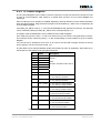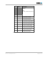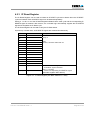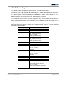
1
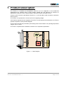
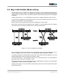
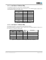
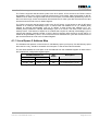
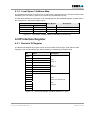
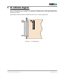
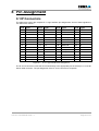
The Embedded I/O Company TCP211 Compact PCI IP Carrier Version 1.0 User Manual Issue 1.1 November 2003 TEWS TECHNOLOGIES GmbH Am Bahnhof 7 Phone: +49-(0)4101-4058-0 e-mail: [email protected] 25469 Halstenbek / Germany Fax: +49-(0)4101-4058-19 www.tews.com TEWS TECHNOLOGIES LLC 1 E. Liberty Street, Sixth Floor Phone: +1 (775) 686 6077 e-mail: [email protected] Reno, Nevada 89504 / USA Fax: +1 (775) 686 6024 www.tews.com TCP211-10 Compact modules PCI Carrier for 2 IndustryPack® This document contains information, which is proprietary to TEWS TECHNOLOGIES GmbH. Any reproduction without written permission is forbidden. TEWS TECHNOLOGIES GmbH has made any effort to ensure that this manual is accurate and complete. However TEWS TECHNOLOGIES GmbH reserves the right to change the product described in this document at any time without notice. TEWS TECHNOLOGIES GmbH is not liable for any damage arising out of the application or use of the device described herein. Style Conventions Hexadecimal characters are specified with prefix 0x, i.e. 0x029E (that means hexadecimal value 029E). For signals on hardware products, an ‚Active Low’ is represented by the signal name with # following, i.e. IP_RESET#. Access terms are described as: W Write Only R Read Only R/W Read/Write R/C Read/Clear R/S Read/Set 2003 by TEWS TECHNOLOGIES GmbH IndustryPack is a registered trademark of SBS Technologies, Inc Issue Description Date 1.0 First Issue February 2003 1.1 Correction Figure “ PCI to Local Byte lane swapping” November 2003 TCP211 User Manual Issue 1.1 Page 2 of 32 Table of Contents 1 2 3 PRODUCT DESCRIPTION ......................................................................................... 5 TECHNICAL SPECIFICATION................................................................................... 6 PCI INTERFACE......................................................................................................... 7 3.1 PCI Configuration (CFG) Registers ...............................................................................................8 3.1.1 PCI Header ...........................................................................................................................8 3.1.2 PCI Base Address Initialization ............................................................................................9 3.1.2.1 I/O Base Address Implementation..............................................................................10 3.1.2.2 Memory Base Address Implementation .....................................................................10 3.1.2.3 Expansion ROM Base Address Implementation ........................................................11 3.2 Local Configuration Register.......................................................................................................12 3.3 Target Configuration EEPROM....................................................................................................13 3.4 Endian Conventions .....................................................................................................................14 3.4.1 Intel CPU View....................................................................................................................15 3.4.2 PowerPC CPU View ...........................................................................................................16 3.4.3 Intel CPU View with TCP211 switched to Big Endian ........................................................17 3.4.4 PowerPC CPU View with TCP211 switched to Big Endian................................................18 3.5 Big / Little Endian Mode setting ..................................................................................................19 4 IP INTERFACE ......................................................................................................... 20 4.1 PCI9030 Local Space Assignment ..............................................................................................20 4.1.1 Local Space 0 Address Map...............................................................................................21 4.1.2 Local Space 1 Address Map...............................................................................................21 4.1.3 Local Space 2 Address Map...............................................................................................22 4.1.4 Local Space 3 Address Map...............................................................................................23 4.2 IP Interface Register .....................................................................................................................23 4.2.1 Revision ID Register ...........................................................................................................23 4.2.2 IP Control Register .............................................................................................................24 4.2.3 IP Reset Register................................................................................................................26 4.2.4 IP Status Register...............................................................................................................27 4.3 IP Interrupts ...................................................................................................................................28 5 6 7 8 IP STROBE SIGNAL ................................................................................................ 29 INSTALLATION OF INDUSTRYPACKS .................................................................. 30 FUSES AND FILTERS ............................................................................................. 31 PIN ASSIGNMENT ................................................................................................... 32 8.1 IP Connectors................................................................................................................................32 TCP211 User Manual Issue 1.1 Page 3 of 32 Table of Figures FIGURE 1-1 : BLOCK DIAGRAM......................................................................................................................5 FIGURE 2-1 : TECHNICAL SPECIFICATION...................................................................................................6 FIGURE 3-1 : PCI CONFIGURATION REGISTER MAP ..................................................................................8 FIGURE 3-2 : LOCAL CONFIGURATION REGISTERS.................................................................................12 FIGURE 3-3 : PCI9030 CONFIGURATION EEPROM CONTENT .................................................................13 FIGURE 3-4 : INTEL CPU VIEW.....................................................................................................................15 FIGURE 3-5 : POWERPC CPU VIEW ............................................................................................................16 FIGURE 3-6 : INTEL CPU VIEW WITH TCP211 SWITCHED TO BIG ENDIAN............................................17 FIGURE 3-7 : POWERPC CPU VIEW WITH TCP211 SWITCHED TO BIG ENDIAN ...................................18 FIGURE 3-8 : PCI TO LOCAL BYTE LANE SWAPPING ...............................................................................19 FIGURE 4-1 : PCI9030 LOCAL SPACE ASSIGNMENT.................................................................................20 FIGURE 4-2 : LOCAL SPACE 0 ADDRESS MAP ..........................................................................................21 FIGURE 4-3 : LOCAL SPACE 1 ADDRESS MAP (IP A-B ID, INT, I/O SPACE)............................................21 FIGURE 4-4 : LOCAL SPACE 2 ADDRESS MAP (IP A-B MEMORY SPACE 16 BIT) ..................................22 FIGURE 4-5 : LOCAL SPACE 3 ADDRESS MAP (IP A-B MEMORY SPACE 8 BIT) ....................................23 FIGURE 4-6 : REVISION ID REGISTER (PCI BASE ADDRESS 2 + 0X00) ..................................................23 FIGURE 4-7 : IP A CONTROL REGISTER (PCI BASE ADDRESS 2 + 0X02)...............................................24 FIGURE 4-8 : IP B CONTROL REGISTER (PCI BASE ADDRESS 2 + 0X04)...............................................25 FIGURE 4-9 : IP RESET REGISTER (PCI BASE ADDRESS 2 + 0X0A) .......................................................26 FIGURE 4-10: IP STATUS REGISTER (PCI BASE ADDRESS 2 + 0X0C)....................................................28 FIGURE 5-1 : IP STROBE SIGNAL ................................................................................................................29 FIGURE 6-1 : I/O PIN ORDER ........................................................................................................................30 FIGURE 8-1 : IP J1 LOGIC INTERFACE PIN ASSIGNMENT........................................................................32 TCP211 User Manual Issue 1.1 Page 4 of 32 1 Product Description The TCP211 is a standard 3U CompactPCI carrier for up to 2 single-size or one double-size IndustryPack (IP) modules used to build modular, flexible and cost effective I/O solutions for applications in process control, medical systems, telecommunication and traffic control. Access to all IP I/O lines is provided by two 50 pin, 0.1 inch flat ribbon cable connectors mounted in the front panel. The TCP211 can operate with 3.3V and 5.0V PCI I/O signaling voltage. All IP interrupt request lines are mapped to PCI INTA. For fast interrupt source detection, the TCP211 provides a special IP Interrupt Status Register. The IP power lines are fuse protected by self healing fuses and RF filtered. The operating temperature range is -40°C to +85°C. The TCP211 complies with the PICMG 2.0 Revision 3.0 CompactPCI specification. Figure 1-1 : Block Diagram TCP211 User Manual Issue 1.1 Page 5 of 32 2 Technical Specification Compact PCI Interface Compact PCI 3U, conforming to PICMG 2.0 R3.0 PCI Interface PCI 2.2 compliant interface, 33 MHz, 32 bit PCI I/O Signaling Voltage 3.3V or 5.0V IP Interface According to IndustryPack specification ANSI / VITA 4-1995 IP Slots Two single-size or one double-size with I/O IP Access 8 / 16 bit 8 / 32 MHz, selectable per IP 8 Mbyte memory space per IP Mapping of IP Interrupts All IP interrupts are mapped to PCI INTA, Local Interrupt Status Register I/O Access Two 50 pin, 0.1 inch flat ribbon cable connectors (stacked version), front panel I/O DMA 32 Bit Access Not supported Not supported Status LEDs No Protection Self healing fuses and RF-filtering on all IP power lines Power Requirements without IP Modules 260 mA typical @ + 5V DC 1 mA typical @ + 12V DC 1 mA typical @ -12V DC Additional power is required by IP modules Temperature Range Operating Storage MTBF 247200 h Weight Tbd Size 160 mm x 100 mm Humidity 5 – 95 % non-condensing – 40°C to + 85°C – 40°C to + 85°C Figure 2-1 : Technical Specification TCP211 User Manual Issue 1.1 Page 6 of 32 3 PCI Interface The TCP211 is accessible in the PCI memory space. The PCI9030 PCI Target Chip from PLX Technology is used as PCI target device for accessing the IP interface. A FPGA is used on the PCI9030 local bus to build the IP interface and provide IP interface control registers. The PCI9030 provides four local spaces 0:3 that are used for the IP interface. Basic PCI9030 register configuration is loaded from a serial EEPROM after power-up or board reset. TCP211 User Manual Issue 1.1 Page 7 of 32 3.1 PCI Configuration (CFG) Registers 3.1.1 PCI Header PCI CFG Register Address Write ‘0’ to all unused (Reserved) bits 31 24 23 16 15 8 7 0x00 Device ID Vendor ID 0x04 Status Command 0x08 0x0C Class Code BIST Header Type PCI Latency Timer PCI write able Read after initialization write access (hex values) N 20D3 1498 0 Y 0280 0003 Revision ID N 068000 00 Cache line Size Y[7:0] 00 00 00 00 0x10 PCI Base Address 0 for Mem Mapped Configuration Registers Y FFFFFF80 0x14 PCI Base Address 1 for I/O Mapped Configuration Registers Y FFFFFF81 0x18 PCI Base Address 2 for Local Address Space 0 Y FFFFFF00 0x1C PCI Base Address 3 for Local Address Space 1 Y FFFFFE00 0x20 PCI Base Address 4 for Local Address Space 2 Y FF000000 0x24 PCI Base Address 5 for Local Address Space 3 Y FF800000 Cardbus CIS Pointer N 00000000 N 200A 1498 Y 00000000 0x28 0x2C Subsystem ID 0x30 Subsystem Vendor ID PCI Base Address for Local Expansion ROM 0x34 Reserved 0x38 0x3C 0x40 Max_Lat Min_Gnt Power Management Capabilities 0x44 Data PMCSR Bridge Support Extensions 0x48 Reserved Control/Status 0x4C Next Cap P. Reserved VPD Address 0x50 N 000000 40 N 00000000 Interrupt Pin Interrupt Line Y[7:0] 00 00 01 00 Next Cap Pointer Capability ID N 4801 48 01 Y 00 00 0000 Power Management Control/Status Next_Cap Pointer Capability ID Y[23:16] 00 02 4C 06 Next_Cap Pointer Capability ID Y[31:16] 0000 00 03 Y 00000000 VPD Data Register Figure 3-1 : PCI Configuration Register Map TCP211 User Manual Issue 1.1 Page 8 of 32 3.1.2 PCI Base Address Initialization PCI host bus-initialization software determines the required address space by an initialization write access (writing a value of all ones ‘1’ to a PCI Base Address Register) and then reading back the value of the PCI Base Address Register. The PCI9030 (PCI Target chip) returns zero ‘0’ in don’t care address bits, specifying the required address space. The PCI software then maps the local address space into the PCI address space by programming the PCI Base Address Register. After programming the required address spaces the user must set bit 0 (enables I/O accesses) and bit 1 (enables memory accesses) of the Command Register (Offset 0x04) to ‘1’. TCP211 User Manual Issue 1.1 Page 9 of 32 3.1.2.1 I/O Base Address Implementation 1. Write a value of ‘1’ to all bits of the PCI Base Address Registers 0 to 5. 2. Check that bit 0 of the register contains a value of ‘1’ (PCI9030 needs an I/O address space). 3. Starting at bit location 2 of the PCI Base Address Register, search for the first bit set to a value of ‘1’. This bit is the binary size of the total contiguous block of I/O address space needed by the PCI9030. For example, if bit 5 of the PCI Base Address Register is detected as the first bit set to ‘1’, the PCI9030 is requesting a 32 byte block of I/O address space. 4. Write the start address of the requested I/O address space to the PCI Base Address Register. The PCI Base Address 1 for I/O Mapped Configuration Registers (128 byte) is used by the TCP211 as I/O address space. 3.1.2.2 Memory Base Address Implementation 1. Write a value of ‘1’ to all bits of the PCI Base Address Registers 0 to 5. 2. Check that bit 0 of the register contains a value of ‘0’ (PCI9030 needs a memory address space). 3. Starting at bit location 4 of the PCI Base Address Register, search for the first bit set to a value of ‘1’. This bit is the binary size of the total contiguous block of memory address space needed by the PCI9030. For example, if bit 15 of the PCI Base Address Register is detected as the first bit set to ‘1’, the PCI9030 is requesting a 32 kilobyte block of memory address space. 4. Write the start address of the requested memory address block to the PCI Base Address Register. This memory address region must not conflict with any other memory space utilized within the system. In addition, it must comply with the definition contained in bits 1 and 2 of this register. The PCI Base Address 0 for Memory Mapped Configuration Registers (128 byte) and the PCI Base Addresses 2 to 5 for Local Address Space 0 to 3 are used by the TCP211 as memory address space. TCP211 User Manual Issue 1.1 Page 10 of 32 3.1.2.3 Expansion ROM Base Address Implementation 5. Write a value of ‘1’ to bits 11 through 31 of PCI Base Address Local Expansion ROM Register. 6. Starting at bit location 11 of the PCI Base Address Local Expansion ROM Register, search upward for the first bit set to a value of ‘1’. This bit is the binary size of the total contiguous block of memory address space needed by the PCI9030. For example, if bit 16 of the PCI Base Address Local Expansion ROM Register is detected as the first bit set, the device is requesting a 64 kilobyte block of memory address space. 7. Write the start address of the requested memory address block to the PCI Base Address Local Expansion ROM Register. This memory address region must not conflict with any other memory space utilized within the system. The Expansion ROM is not used by the TCP211. For further information please refer to the PCI9030 manual which is also part of the TCP211-ED Engineering Documentation. TCP211 User Manual Issue 1.1 Page 11 of 32 3.2 Local Configuration Register After reset, the Local Configuration Registers (LCRs) are loaded from the on board EEPROM. The LCRs are accessible in the PCI Base Address 0 Memory Mapped or in the PCI Base Address 1 I/O Mapped Configuration Registers. Do not change the value of these registers because these values are hardware dependent. PCI (Offset from Local Base Address) Register Value Description 0x00 Local Address Space 0 Range 0x0FFFFF00 IP Interface Register (256 byte) 0x04 Local Address Space 1 Range 0x0FFFFE00 IP A-B ID , INT , I/O Space (512Byte) 0x08 Local Address Space 2 Range 0x0F000000 IP A-B MEM Space (16 bit) (16Mbyte) 0x0C Local Address Space 3 Range 0x0F800000 IP A-B MEM Space (8 bit) (8Mbyte) 0x10 Local Exp. ROM Range 0x00000000 Not used 0x14 Local Re-map Register Space 0 0x08000001 Enabled 0x18 Local Re-map Register Space 1 0x04000001 Enabled 0x1C Local Re-map Register Space 2 0x00000001 Enabled 0x20 Local Re-map Register Space 3 0x02000001 Enabled 0x24 Local Re-map Register ROM 0x00000000 Not used 0x28 Local Address Space 0 Descriptor 0xD44160A0 Timing local Space 0 0x2C Local Address Space 1 Descriptor 0x144120A2 Timing local Space 1 0x30 Local Address Space 2 Descriptor 0x144120A2 Timing local Space 2 0x34 Local Address Space 3 Descriptor 0x140120A2 Timing local Space 3 0x38 Local Exp. ROM Descriptor 0x00000000 Not used 0x3C Chip Select 0 Base Address 0x08000081 CS for local Space 0 0x40 Chip Select 1 Base Address 0x04000201 CS for local Space 1 0x44 Chip Select 2 Base Address 0x01000001 CS for local Space 2 0x48 Chip Select 3 Base Address 0x02800001 CS for local Space 3 0x4C Interrupt Control/Status 0x00000041 Interrupt Configuration 0x4E EEPROM Write Protect Boundary 0x00000000 No write protection 0x50 Miscellaneous Control Register 0x007A4000 Retry Delay = max 0x54 General Purpose I/O Control 0x02249252 GPI/O2=CS2# GPI/O3=CS3# 0x70 Hidden 1 Power Management data select 0x00000000 Not used 0x74 Hidden 2 Power Management data scale 0x00000000 Not used Figure 3-2 : Local Configuration Registers TCP211 User Manual Issue 1.1 Page 12 of 32 3.3 Target Configuration EEPROM After reset, the PCI9030 starts to load the configuration sequence from the on board EEPROM. This EEPROM contains the following configuration data. • From 0x00 to 0x27 : PCI Configuration • From 0x28 to 0x87 : Local Configuration EEPROM Address 0x00 0x02 0x04 0x06 0x08 0x0A 0x0C 0x0E 0x00 0x20D3 0x1498 0x0280 0x0000 0x0680 0x0000 0x200A 0x1498 0x10 0x0000 0x0100 0x4801 0x0001 0x0000 0x0000 0x0000 0x0040 0x20 0x0000 0x4C06 0x0000 0x0003 0x0FFF 0xFF00 0x0FFF 0xFE00 0x30 0x0F00 0x0000 0x0F80 0x0000 0x0000 0x0000 0x0800 0x0001 0x40 0x0400 0x0001 0x0000 0x0001 0x0200 0x0001 0x0000 0x0000 0x50 0xD441 0x60A0 0x1441 0x20A2 0x1441 0x20A2 0x1401 0x20A2 0x60 0x0000 0x0000 0x0800 0x0081 0x0400 0x0201 0x0100 0x0001 0x70 0x0280 0x0001 0x0000 0x0041 0x007A 0x4000 0x0224 0x9252 0x80 0x0000 0x0000 0x0000 0x0000 0xFFFF 0xFFFF 0xFFFF 0xFFFF 0x90 0xFFFF 0xFFFF 0xFFFF 0xFFFF 0xFFFF 0xFFFF 0xFFFF 0xFFFF 0xA0 0xFFFF 0xFFFF 0xFFFF 0xFFFF 0xFFFF 0xFFFF 0xFFFF 0xFFFF 0xB0 0xFFFF 0xFFFF 0xFFFF 0xFFFF 0xFFFF 0xFFFF 0xFFFF 0xFFFF 0xC0 0xFFFF 0xFFFF 0xFFFF 0xFFFF 0xFFFF 0xFFFF 0xFFFF 0xFFFF 0xD0 0xFFFF 0xFFFF 0xFFFF 0xFFFF 0xFFFF 0xFFFF 0xFFFF 0xFFFF 0xE0 0xFFFF 0xFFFF 0xFFFF 0xFFFF 0xFFFF 0xFFFF 0xFFFF 0xFFFF 0xF0 0xFFFF 0xFFFF 0xFFFF 0xFFFF 0xFFFF 0xFFFF 0xFFFF 0xFFFF Figure 3-3 : PCI9030 Configuration EEPROM Content TCP211 User Manual Issue 1.1 Page 13 of 32 3.4 Endian Conventions This chapter tries to illuminate the mixed use of Big Endian and Little Endian convention in one system. The major difference between Big Endian and Little Endian are swapped byte lanes. The byte lanes for 16 bit and 32 bit data busses with Big Endian and Little Endian are shown below: Little Endian convention on a 16 bit Data Bus: Byte Lane Byte 1 Byte 0 Data Line D15 : D8 D7 : D0 (LSB) Big Endian convention on a 16 bit Data Bus: Byte Lane Byte 0 Byte 1 Data Line D15 : D8 D7 : D0 (LSB) Little Endian convention on a 32 bit Data Bus: Byte Lane Byte 3 Byte 2 Byte 1 Byte 0 Data Line D31 : D24 D23 : D16 D15 : D8 D7 : D0 (LSB) Big Endian convention on a 32 bit Data Bus: Byte Lane Byte 0 Byte 1 Byte 2 Byte 3 Data Line D31 : D24 D23 : D16 D15 : D8 D7 : D0 (LSB) The PCI Bus and all Intel CPUs work in Little Endian mode. VMEbus, PowerPC and 68K CPUs work in Big Endian mode. Most IP modules, which are common in VMEbus systems, also use Big Endian byte ordering. The TCP211 works in Little Endian mode by default, but can be switched to work in Big Endian mode. This leads to 4 major Big- Little Endian combinations in one system: - Little Endian CPU with TCP211 (Little Endian) and IP module (Big Endian) - Little Endian CPU with TCP211 (Big Endian) and IP module (Big Endian) - Big Endian CPU with TCP211 (Big Endian) and IP module (Big Endian) - Big Endian CPU with TCP211 (Little Endian) and IP module (Big Endian) See the next four subchapters for a detailed view on these combinations. TCP211 User Manual Issue 1.1 Page 14 of 32 3.4.1 Intel CPU View Figure 3-4 : Intel CPU View TCP211 User Manual Issue 1.1 Page 15 of 32 3.4.2 PowerPC CPU View Figure 3-5 : PowerPC CPU View TCP211 User Manual Issue 1.1 Page 16 of 32 3.4.3 Intel CPU View with TCP211 switched to Big Endian Figure 3-6 : Intel CPU View with TCP211 switched to Big Endian TCP211 User Manual Issue 1.1 Page 17 of 32 3.4.4 PowerPC CPU View with TCP211 switched to Big Endian Figure 3-7 : PowerPC CPU View with TCP211 switched to Big Endian TCP211 User Manual Issue 1.1 Page 18 of 32 3.5 Big / Little Endian Mode setting The PCI target chip of the TCP211, the PCI9030 can be set to convert to Big Endian data ordering on the local bus. This is useful for IP modules that use Big Endian byte ordering. Big Endian byte ordering is the convention used in the Motorola 68000 microprocessor family and is the VMEbus convention. Changing local space 0, 1 or 2 to Big Endian mode results in swapped data lines of the local bus: A 32 bit access is separated by the PCI9030 into two local 16 bit accesses. Byte lane 0 and 1 are swapped, and byte lane 2 and 3 are swapped. During 16 bit access, the upper and lower bytes are displayed in reverse order. During 8 bit access odd and even addresses are swapped. To access Address 0x00, the Address 0x01 must be used. An access to Address 0x01 is done by Address 0x00. Figure 3-8 : PCI to Local Byte lane swapping The local Endian mode of the PCI9030 can be changed for each local space separately. This is done by changing the value of bit 24 in the corresponding Bus Region Descriptor Register: To change local space 0, that provides access to the local control and status registers, from Little Endian to Big Endian mode, write 0xD5 to PCI BAR0 + 0x2B. To change local space 1, that provides access to IP I/O- ID and INT space, from Little Endian to Big Endian mode, write 0x15 to PCI BAR0 + 0x2F. To change local space 2, that provides access to the IP MEM space (16 bit port), from Little Endian to Big Endian mode, write 0x15 to PCI BAR0 + 0x33. Changing local space 3 from Little Endian to Big Endian mode has no effect, because this space has only an 8 bit port. TCP211 User Manual Issue 1.1 Page 19 of 32 4 IP Interface The IP FPGA provides the interface between the PCI9030 local bus and the IP slots. The IP FPGA also provides the IP Interface Control Registers. A PCI access to the TCP211 will be terminated in every case. If the IP does not generate an ACK#, a local timeout will terminate the IP access after a timeout time of 8µs and the timeout bit is set in the IP Status Register. All F’s are returned for read cycles. The IP FPGA is configured at power-up by an on board serial PROM. 4.1 PCI9030 Local Space Assignment The PCI9030 local spaces must be used to access the IP Interface. The PCI base address for each local space can be obtained from the PCI9030 PCI configuration register space. Space 0 contains the IP Control and Status Register. Space 1 provides access to I/O ID and INT space of all IPs. Space 2 is used for the IP A-B Memory space. Space 3 is also used for IP A-B Memory space, but provides linear addressing for IP modules, that use only D7:0. PCI9030 Local Space Size (Byte) Port Width (Bit) Endian Mode IP Interface Space 0 256 16 Little IP Interface Register 1 512 16 Little IP A-B ID, INT, I/O Space 2 16M 16 Little IP A-B MEM Space (16 bit) 3 8M 8 Little IP A-B MEM Space (8 bit) Figure 4-1 : PCI9030 Local Space Assignment TCP211 User Manual Issue 1.1 Page 20 of 32 4.1.1 Local Space 0 Address Map The PCI9030 local space 0 is used for the IP Interface Registers. The PCI base address for local space 0 can be obtained from the PCIBAR2 Register at offset 0x18 in the PCI9030 PCI configuration register space. PCI Base Address 2 + Size(Byte) Register 0x00 2 REVISION ID 0x02 2 IP A CONTROL 0x04 2 IP B CONTROL 0x06 2 reserved 0x08 2 reserved 0x0A 2 RESET 0x0C 2 STATUS 0x0E 2 reserved 0x10 - 0xFF 240 reserved Figure 4-2 : Local Space 0 Address Map 4.1.2 Local Space 1 Address Map The PCI9030 local space 1 is used for the IP A-B ID, INT and I/O space. The PCI base address for local space 1 can be obtained from the PCIBAR3 Register at offset 0x1C in the PCI9030 PCI configuration register space. PCI Base Address 3 + Start End Size (Byte) Description 0x0000_0000 0x0000_007F 128 IP A I/O Space 0x0000_0080 0x0000_00BF 64 IP A ID Space 0x0000_00C0 0x0000_00FF 64 IP A INT Space 0x0000_0100 0x0000_017F 128 IP B I/O Space 0x0000_0180 0x0000_01BF 64 IP B ID Space 0x0000_01C0 0x0000_01FF 64 IP B INT Space Figure 4-3 : Local Space 1 Address Map (IP A-B ID, INT, I/O Space) TCP211 User Manual Issue 1.1 Page 21 of 32 The TCP211 supports read and write cycles to the IP I/O space. The TCP211 supports read and write cycles to the IP ID space. A PCI access to the TCP211 will be terminated in every case. If the IP supports write access to its ID space, data will be written to the IDPROM. If the IP does not support write access to its ID space, no ACK# will be generated by the IP to the local control logic, and a local timeout will terminate the IP write cycle after a timeout time of 8µs and the timeout bit is set in the IP Status Register. The TCP211 supports read and write cycles to the IP INT space. A read access to the IP INT space initiates an IP interrupt acknowledge cycle. A read access with address A1=0 (i.e. 0x0000_00c0) initiates an interrupt acknowledge cycle for IP INT0#, a read access with address A1=1 (i.e. 0x0000_00C2) initiates an interrupt acknowledge cycle for IP INT1#. The read access returns the interrupt vector. This feature is helpful for IP modules that require an interrupt acknowledge cycle to remove their pending interrupt request. If the IP does not support write access to its INT space, no ACK# will be generated by the IP, and a local timeout will terminate the cycle after a timeout time of 8µs and the timeout bit is set in the IP Status Register. 4.1.3 Local Space 2 Address Map The PCI9030 local space 2 is used for the IP A-B Memory space (16 bit port). IPs with Memory space that uses D7:0 only, should be accessed via local space 3. See section below for details. The PCI base address for local space 2 can be obtained from the PCIBAR4 Register at offset 0x20 in the PCI9030 PCI configuration register space. Start End Size (Byte) 0x0000_0000 0x007F_FFFF 8M IP A MEM Space (16 bit) 0x0080_0000 0x00FF_FFFF 8M IP B MEM Space (16 bit) PCI Base Address 4 + Description Figure 4-4 : Local Space 2 Address Map (IP A-B Memory Space 16 bit) TCP211 User Manual Issue 1.1 Page 22 of 32 4.1.4 Local Space 3 Address Map The PCI9030 local space 3 is used for the IP A-B memory space (8 bit port). This space allows linear addressing of the IP memory space for IP’s with 8 bit port width (D0-D7) only. The PCI base address for local space 3 can be obtained from the PCIBAR5 Register at offset 0x24 in the PCI9030 PCI configuration register space. Offset (Base = PCI Base Address 5) Size (Byte) Description Start End 0x0000_0000 0x003F_FFFF 4M IP A MEM Space (8 bit) 0x0040_0000 0x007F_FFFF 4M IP B MEM Space (8 bit) Figure 4-5 : Local Space 3 Address Map (IP A-B Memory Space 8 bit) 4.2 IP Interface Register 4.2.1 Revision ID Register The Revision ID Register shows the revision of the on board IP FPGA logic. Initial Value is 0x00. Changes in the on board FPGA logic will be signed by incrementing the register value. Bit Name 15 (MSB) - 14 - 13 - 12 - 11 - 10 - 9 - 8 - 7 REV_ID Description Read: Always 0 Write: No Effect 6 5 4 3 2 Read: FPGA Logic Revision ID Write: No Effect 1 0 (LSB) Figure 4-6 : Revision ID Register (PCI Base Address 2 + 0x00) TCP211 User Manual Issue 1.1 Page 23 of 32 4.2.2 IP Control Register The IP Control Registers can be used to control IP interrupts, recover time and clock rate. Each IP has its own IP Control Register. After power-up or board reset, all bits in the IP Control Register are cleared (0). Each IP interrupt can be enabled or disabled separately. Interrupt detection can be switched between level and edge sensitive. Edge sensitive interrupts must be cleared by a write to the corresponding bit in the IP Status Register. If the ERR_INT_EN bit is set to "1", an active IP ERROR# line will generate an interrupt. This interrupt can be cleared by setting the ERR_INT_EN bit of the corresponding IP to "0". The status of the IP ERROR# line can be read from the IP Status Register. If the TIME_INT_EN bit is set to “1” and an IP timeout occurs, the TCP211 will generate an interrupt. This interrupt can be cleared by writing ‘1’ to the corresponding IP timeout status bit in the IP Status Register. If IP recover time is enabled for an IP slot, an IP cycle for this slot will not begin until the IP recover time is expired. The IP recover time is app. 1µs. IP Clock Rate can be selected between 8 MHz and 32 MHz for each IP separately. After power-up or board reset, the Clock Rate is set to 8 MHz for both IPs. Bit Name 15 (MSB) - Description Read: Always 0 14 - 13 - 12 - 11 - 10 - 9 - 8 - 7 INT1_EN 0 : IP A interrupt 1 disabled 1 : IP A interrupt 1 enabled 6 INT0_EN 0 : IP A interrupt 0 disabled 1 : IP A interrupt 0 enabled 5 INT1_SENSE 0 : IP A interrupt 1 level sensitive 1 : IP A interrupt 1 edge sensitive 4 INT0_SENSE 0 : IP A interrupt 0 level sensitive 1 : IP A interrupt 0 edge sensitive 3 ERR_INT_EN 0 : IP A error interrupt disabled 1 : IP A error interrupt enabled 2 TIME_INT_EN 0 : IP A timeout interrupt disabled 1 : IP A timeout interrupt enabled 1 RECOVER 0 : IP A recover time disabled 1 : IP A recover time enabled 0 (LSB) CLKRATE 0 : IP A clock rate 8 MHz 1 : IP A clock rate 32 MHz Write: No effect, should be written with 0's Figure 4-7 : IP A Control Register (PCI Base Address 2 + 0x02) TCP211 User Manual Issue 1.1 Page 24 of 32 Bit Name 15 (MSB) - Description Read : Always 0 14 - 13 - 12 - 11 - 10 - 9 - 8 - 7 INT1_EN 0 : IP B interrupt 1 disabled 1 : IP B interrupt 1 enabled 6 INT0_EN 0 : IP B interrupt 0 disabled 1 : IP B interrupt 0 enabled 5 INT1_SENSE 0 : IP B interrupt 1 level sensitive 1 : IP B interrupt 1 edge sensitive 4 INT0_SENSE 0 : IP B interrupt 0 level sensitive 1 : IP B interrupt 0 edge sensitive 3 ERR_INT_EN 0 : IP B error interrupt disabled 1 : IP B error interrupt enabled 2 TIME_INT_EN 0 : IP B timeout interrupt disabled 1 : IP B timeout interrupt enabled 1 RECOVER 0 : IP B recover time disabled 1 : IP B recover time enabled 0 (LSB) CLKRATE 0 : IP B clock rate 8 MHz 1 : IP B clock rate 32 MHz Write: No effect, should be written with 0's Figure 4-8 : IP B Control Register (PCI Base Address 2 + 0x04) TCP211 User Manual Issue 1.1 Page 25 of 32 4.2.3 IP Reset Register The IP Reset Register can be used to initiate an IP RESET cycle and to detect when the IP RESET cycle has finished. Each IP RESET# signal can be asserted separately. Writing a ‘1’ to bit 1 or 0 of the IP Reset Register initiates that the reset cycle and the corresponding IP RESET# signal is asserted. After 200 ms, the on board logic automatically negates the IP RESET# signal and completes the IP Reset cycle. The IP Reset Register can be read to verify the IP Reset status. At power-up or board reset, all IP RESET# signals are asserted simultaneously. Name Description 15 (MSB) Bit - 14 - Read: Always 0 13 - 12 - 11 - 10 - 9 - 8 - 7 - 6 - 5 - 4 - 3 - 2 - 1 IPB_RESET 0 (LSB) IPA_RESET Write: No effect, should be written with 0's Read: 0 : IP RESET# signal is de-asserted 1 : IP RESET# signal is asserted Write: 0 : No effect 1 : Assert corresponding IP RESET# signal (automatic negation after 200 ms) Figure 4-9 : IP Reset Register (PCI Base Address 2 + 0x0A) TCP211 User Manual Issue 1.1 Page 26 of 32 4.2.4 IP Status Register The IP Status Register can be used to read IP timeout, error and interrupt status. An IP timeout occurs if the IP module fails to generate the IP ACK# signal within the IP timeout time. The IP timeout time is app. 8µs. An IP timeout is not reported to the PCI9030 or the PCI master, but in the IP Status Register. If the corresponding IP_TIME_EN bit in the IP Control Register is set, an interrupt is generated if a timeout occurs. This interrupt can be cleared by writing ‘1’ to the timeout status bit. If a timeout occurs during an IP read, all ones (0xFF) are returned. The IP ERROR# signal is used to indicate component failure, unrecoverable self-test failures or serious, hard-wired configuration errors. The status of the IP ERROR# signals can be read in the IP Status Register. Interrupt status of all IP interrupt lines can read in the IP Status Register. If edge sensitive interrupt is enabled (see IP Control Register for detail) and an interrupt is active, writing a “1” to bit 3:0 clears the corresponding interrupt status. Bit Name Description 15 (MSB) - reserved 14 - reserved 13 TIME_B Read : 0 : IP_B timeout has not occurred 1 : IP_B timeout has occurred Write : 0 : No effect 1 : Clear IP_B timeout status 12 TIME_A Read : 0 : IP_A timeout has not occurred 1 : IP_A timeout has occurred Write : 0 : No effect 1 : Clear IP_A timeout status 11 - reserved 10 - reserved 9 ERR_B Read : 0 : IP_B ERROR# signal de-asserted 1 : IP_B ERROR# signal asserted Write : 0 : No effect 1 : No effect 8 ERR_A Read : 0 : IP_A ERROR# signal de-asserted 1 : IP_A ERROR# signal asserted Write : 0 : No effect 1 : No effect 7 - reserved 6 - reserved 5 - reserved 4 - reserved 3 INT1_B Read : 0 : No IP_B interrupt 1 request 1 : Active IP_B interrupt 1 request Write : 0 : No effect 1 : Clear edge sensitive IP_B interrupt 1 status TCP211 User Manual Issue 1.1 Page 27 of 32 Bit Name Description 2 INT0_B Read : 0 : No IP_B interrupt 0 request 1 : Active IP_B interrupt 0 request Write : 0 : No effect 1 : Clear edge sensitive IP_B interrupt 0 status 1 INT1_A Read : 0 : No IP_A interrupt 1 request 1 : Active IP_A interrupt 1 request Write : 0 : No effect 1 : Clear edge sensitive IP_A interrupt 1 status 0 (LSB) INT0_A Read : 0 : No IP_A interrupt 0 request 1 : Active IP_A interrupt 0 request Write : 0 : No effect 1 : Clear edge sensitive IP_A interrupt 0 status Figure 4-10: IP Status Register (PCI Base Address 2 + 0x0C) 4.3 IP Interrupts All IP interface interrupt sources (Timeout, Error, IP A-B INT0, IP A-B INT1) are mapped to PCI interrupt INTA#. For quick interrupt source detection, the IP Status Register can be read to determine the IP interrupt source. Level sensitive IP interrupts, which are most common for IP modules are cleared by either an interrupt acknowledge cycle to the IP or by accessing an Interrupt Status Register on the IP module. A read access to the IP INT space initiates an IP interrupt acknowledge cycle. A read access with address A1=0 (i.e. 0x0000_00c0) initiates an interrupt acknowledge cycle for IP INT0#, a read access with address A1=1 (i.e. 0x0000_00C2) initiates an interrupt acknowledge cycle for IP INT1#. The read access returns the interrupt vector. This feature is helpful for IP modules that require an interrupt acknowledge cycle to remove their pending interrupt request. Timeout interrupts and edge sensitive IP interrupts must be cleared in the IP Status Register. IP error interrupts must be cleared in the corresponding IP Control Register. TCP211 User Manual Issue 1.1 Page 28 of 32 5 IP Strobe Signal The IP strobe signal is an uncommitted line of the IP logic interface, which may be used as an optional input to or output from an IP module. It is reserved for a digital strobe or clock signal related to the functionality of the IP. Strobe signals of all IP slots are accessible on the TCP211 via a 2-pin jumper field. Figure 5-1 : IP Strobe Signal TCP211 User Manual Issue 1.1 Page 29 of 32 6 Installation of IndustryPacks Before installing an IndustryPack, be sure that the power supply for the TCP211 is turned off. The component is an Electrostatic Sensitive Device (ESD). Use an anti-static mat connected to a wristband when handling or installing the components. Installing IndustryPacks on the TCP211 is done by simply snapping them into one of the two IP slots. The connectors are keyed, so the IndustryPack can only be installed correctly. After an IP has been installed it can be secured on the carrier board. This is normally necessary only in high vibration or shock environments. Screws and spacers are required to fix a single IP on the TCP211. They can be ordered from TEWS TECHNOLOGIES (Part number: TIPxxx-HK). All IPs mate with a 50-pin flat ribbon cable connectors for their I/O. The PCB and front panel labeling indicates, which connector is associated with the according IP slot. Pin 1 for each cable is identified by the mark on the connector or a square solder pad. Figure 6-1 : I/O Pin Order TCP211 User Manual Issue 1.1 Page 30 of 32 7 Fuses and Filters All IP slots are fuse protected. The fuses used on the TCP211 are self-healing fuses. For improved performance the TCP211 provides RF filtering and decoupling capacitors on all IP power lines. TCP211 User Manual Issue 1.1 Page 31 of 32 8 Pin Assignment 8.1 IP Connectors The table below shows the complete IP J1 logic interface pin assignments. Some of these signals are not used on the TCP211. Pin # Signal Pin # Signal Pin # Signal Pin # Signal 1 GND 2 CLK 26 GND 27 +5V 3 Reset# 4 D0 28 R/W# 29 IDSel# 5 D1 6 D2 30 DMAReq0# 31 MemSel# 7 D3 8 D4 32 DMAReq1# 33 IntSel# 9 D5 10 D6 34 DMAck# 35 IOSel# 11 D7 12 D8 36 Reserved 37 A1 13 D9 14 D10 38 DMAEnd# 39 A2 15 D11 16 D12 40 Error# 41 A3 17 D13 18 D14 42 IntReq0# 43 A4 19 D15 20 BS0# 44 IntReq1# 45 A5 21 BS1# 22 -12V 46 Strobe# 47 A6 23 +12V 24 +5V 48 ACK# 49 Reserved 25 GND 50 GND Figure 8-1 : IP J1 Logic Interface Pin Assignment The IP J2 I/O connector routes the IP I/O lines directly to the appropriate pins of the 50 pin 0.1 inch flat ribbon cable connector. The pin assignment of the IP J2 I/O connector is IP specific. TCP211 User Manual Issue 1.1 Page 32 of 32