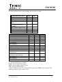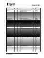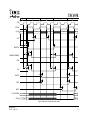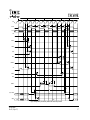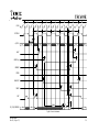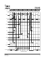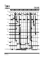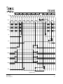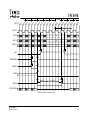
1
TSC693E TSC693E Memory Controller User's Manual For Embedded Real time 32-bit Computer (ERC32) for SPACE Applications MATRA MHS Rev. D (10 Apr. 97) 1 TSC693E TABLE OF CONTENTS Page 1. 1.1. 1.2. 1.2.1. 1.2.2. 1.3. 1.4. 1.4.1. 1.4.2. 1.4.3. INTRODUCTION ....................................................................................... 4 Scope ......................................................................................................... 4 Documents................................................................................................. 5 Applicable Documents............................................................................ 5 Reference Documents ............................................................................. 5 Glossary..................................................................................................... 6 Definitions................................................................................................. 7 Bit Numbering ........................................................................................ 7 Signal Names .......................................................................................... 7 Registers.................................................................................................. 7 2. 2.1. GENERAL OVERVIEW OF ERC32.......................................................... 8 ERC32 Overview ...................................................................................... 8 3. 3.1. 3.2. 3.2.1. 3.2.2. 3.2.2.1. 3.2.3. 3.2.3.1. 3.2.4. 3.2.5. 3.2.5.1. 3.2.6. 3.3. 3.4. 3.5. 3.5.1. 3.5.2. 3.5.3. 3.5.4. 3.5.5. 3.6. 3.7. 3.7.1. 3.7.2. 3.7.3. 3.8. 3.9. 3.9.1. 3.9.2. 3.9.3. MEMORY CONTROLLER FUNCTIONS............................................... 10 Data Types............................................................................................... 12 Memory Interface .................................................................................... 12 Memory Control Signals....................................................................... 12 RAM ..................................................................................................... 12 Extended RAM ................................................................................... 13 Boot PROM .......................................................................................... 14 Extended PROM................................................................................. 14 Exchange Memory ................................................................................ 15 I/O ......................................................................................................... 15 Extended I/O....................................................................................... 17 MEC Memory Map............................................................................... 18 DMA Interface......................................................................................... 19 Bus Arbiter .............................................................................................. 20 Execution Modes..................................................................................... 20 Reset Mode ........................................................................................... 22 Run Mode.............................................................................................. 22 System Halt Mode................................................................................. 22 Power-Down Mode............................................................................... 23 Error Halt Mode.................................................................................... 23 Wait-State and Timeout Generator.......................................................... 23 Memory Access Protection...................................................................... 24 Unimplemented Areas .......................................................................... 24 RAM Write Access Protection.............................................................. 25 Boot PROM Write Protection............................................................... 26 Register Access Protection...................................................................... 26 EDAC ...................................................................................................... 27 Check Bit Generator.............................................................................. 28 Syndrome Generator ............................................................................. 29 Syndrome Detector ............................................................................... 30 MATRA MHS Rev. D (10 Apr. 97) 2 TSC693E 3.9.4. 3.9.5. 3.10. 3.11. 3.12. 3.13. 3.14. 3.15. 3.16. 3.17. 3.18. 3.19. 3.19.1. 3.19.2. 3.19.3. 3.19.4. 3.19.5. 3.20. 3.21. 3.21.1. 3.21.2. Fault Injection ....................................................................................... 31 Memory and I/O Parity ......................................................................... 31 Memory Redundancy .............................................................................. 32 Synchronous Traps .................................................................................. 32 Interrupts (Asynchronous Traps)............................................................. 33 General Purpose and Real Time Clock Timers ....................................... 36 Watch Dog............................................................................................... 38 UART ...................................................................................................... 40 Parity Checking ....................................................................................... 41 Error Handler........................................................................................... 42 System Availability ................................................................................. 47 Test mode and Test Access Port.............................................................. 47 EDAC Test............................................................................................ 47 Parity Test ............................................................................................. 47 Interrupt Test......................................................................................... 47 Error Test .............................................................................................. 48 Test Access Port (TAP) ........................................................................ 48 System Clock........................................................................................... 48 MEC Registers ........................................................................................ 49 Register Address Map........................................................................... 49 Register Configuration and Bit Allocation ........................................... 50 4. 4.1. 4.2. 4.2.1. 4.2.2. 4.2.3. 4.2.4. 4.2.5. 4.2.6. MEMORY CONTROLLER SIGNAL DESCRIPTIONS ......................... 63 Memory Controller Signal Summary ...................................................... 63 MEC Detailed Signal Descriptions ......................................................... 65 IU/FPU Interface Signals ...................................................................... 65 Memory System Interface Signals ........................................................ 71 Interrupt and Control Signals................................................................ 75 Test Access Port Signals....................................................................... 77 UART Interface..................................................................................... 78 Power and Clock Signals ...................................................................... 79 5. 5.1. 5.1.1. 5.1.2. 5.1.3. 5.1.4. 5.2. 5.2.1. 5.2.2. ELECTRICAL AND MECHANICAL SPECIFICATION........................ 80 Maximum Rating and DC Characteristics .............................................. 80 Maximum Ratings................................................................................. 80 Operating Range ................................................................................... 80 DC Characteristics over the Operating Range ...................................... 80 Capacitance Ratings.............................................................................. 81 Package Description ................................................................................ 81 Pin Assignments.................................................................................... 81 Package Diagram .................................................................................. 82 APPENDIX 1 - TIMING DIAGRAMS MATRA MHS Rev. D (10 Apr. 97) 3 TSC693E 1. INTRODUCTION 1.1. Scope This document constitutes a functional specification of iteration two of the TSC693E Memory Controller (MEC) which is an element in the ERC32 microprocessor core. It is intended to function as a User's guide both for the software and hardware developers. The document is divided into the following sections: • GENERAL OVERVIEW OF ERC32 A short overview of a typical ERC32 based system. • TSC693E MEMORY CONTROLLER FUNCTIONS Detailed description of the MEC functions including software interface. • TSC693E MEMORY CONTROLLER SIGNAL DESCRIPTIONS Functional description of MEC signals. • TSC693E ELECTRICAL AND MECHANICAL SPECIFICATION • TIMING DIAGRAMS (APPENDIX 1) Timing specifications and diagrams. MATRA MHS Rev. D (10 Apr. 97) 4 TSC693E 1.2. Documents 1.2.1. Applicable Documents AD1 ESA 32-Bit Microprocessor and Computer Development Programme Statement of Work, WDI/JG/1317/NL, Issue 2.1, 28-05-1991. AD2 Specification for a 32-bit embedded computing core (ERC32), WDI/JG/1334/NL, Issue 3, 29-05-1991. AD3 32-bit Microprocessor Software Tools Technical Requirements, WDI/1339/FGM/NL, 05-06-1991. AD4 ERC32 Technical Specification, MCD/SPC/0001/SE, issue 7, 1 Apr 1994. 1.2.2. Reference Documents RD1 SPARC Standard Version 7 RD2 TSC691E Integer Unit RD3 TSC692E Floating Point Unit User's Manual MATRA MHS Rev. D (10 Apr. 97) 5 TSC693E 1.3. Glossary AD Applicable Document ASI Address Space Identifier ATAC Ada TAsking Coprocessor CS Chip Select DMA Direct Memory Access EDAC Error Detection And Correction EEPROM Electrically Erasable Programmable Read Only Memory ERC32 32 bit Embedded Real-time Computing Core EXM EXchange Memory FAR Failing Address Register FPU Floating Point Unit I/O Input/Output ICR Interrupt Clear Register IFR Interrupt Force Register IMR Interrupt Mask Register IPR Interrupt Pending Register IU Integer Unit MEC MEmory Controller PROM Programmable Read Only Memory RAM Random Access Memory RD Reference Document ROM Read Only Memory RTC Real Time Clock SFSRSystem Fault Status Register SW Software TAP Test Access Port TBC To Be Confirmed TBD To Be Defined UART Universal Asynchronous Receiver Transmitter WD Watch Dog MATRA MHS Rev. D (10 Apr. 97) 6 TSC693E 1.4. Definitions 1.4.1. Bit Numbering In this document the following conventions are used: - The most significant bit in a vector has the highest bit number and the leftmost position in a field. The least significant bit in a vector has the lowest bit number and the rightmost position in a field. 1.4.2. Signal Names The following conventions are used for signal names: - Signal names are written in capital letters, SIGNALNAME. Active low signals are named, SIGNALNAME*. 1.4.3. Registers The following convention is used for registers. - Register names are bolded, Register Name. MATRA MHS Rev. D (10 Apr. 97) 7 TSC693E 2. GENERAL OVERVIEW OF ERC32 2.1. ERC32 Overview The objective of the ERC32 is to provide a high performance 32-bit computing core for on-board embedded real-time computers. The core is characterized by low circuit complexity and power consumption. Extensive concurrent error detection and support for fault-tolerance and reconfiguration is emphasized. In addition to the main objective, the ERC32 core is possible to use for performance demanding research applications in deep space probes. In addition to the above characteristics the radiation tolerance and error masking are important. By including support for reconfigurable of the error handling the different demands from the applications can be optimized for the best purpose in each case. The ERC32 is to be used as a building block only requiring memory and application specific peripherals to be added to form a complete on-board computer. All other system support functions are provided by the core. The ERC32 incorporates the followings functions: - Processor, which consists of one Integer Unit: TSC691E (called IU in this document) and one Floating Point Unit: TSC692E (called FPU in this document). The processor includes concurrent error detection facilities. - Memory Controller: TSC693E (called MEC in this document), which is a unit consisting of all necessary support functions such as memory control and protection, EDAC, wait state generator, timers, interrupt handler, watch dog, UARTs, and test support. The unit also includes concurrent error detection facilities. - One or two oscillator(s). - Buffers necessary to interface with memory and peripherals. Figure 1 schematically shows a basic ERC32 computer with external functions added to form a complete system. MATRA MHS Rev. D (10 Apr. 97) 8 TSC693E Ctrl Hold Error MEC IU Ctrl FPU Data Ctrl Address ERC32 Check bits BOOT PROM Check bits RAM I/O IRQ IRQ ATAC External IRQs Figure 1 - ERC32 Computer with typical peripherals MATRA MHS Rev. D (10 Apr. 97) 9 TSC693E 3. MEMORY CONTROLLER FUNCTIONS All support functions of the ERC32 except for the local clock/oscillator and address and data bus drivers (buffers and latches) are incorporated in one single chip memory controller unit (MEC). The MEC is designed to interface the IU and the FPU to external memory and I/O units thus forming a system, with which computers for on-board embedded real-time applications can be built. In order to achieve this the MEC constitutes all necessary support and on-chip resources accordingly: - System start up control and reset Power down mode control System clock Watchdog function Memory interface to RAM ranging from 256 Kbyte to 32 Mbyte Memory interface to PROM ranging from 128 Kbyte to 4 Mbyte I/O interface to exchange memory (e.g. DPRAM) ranging from 4 Kbyte to 512 Kbyte. I/O interface to four peripherals DMA interface Bus arbiter Programmable wait-state generator Programmable memory access protection Memory redundancy control EDAC, with byte and halfword write support Trap handler including 15-level interrupt controller One 32-bit general purpose timer with 16-bit scaler One 32-bit timer with 8-bit scaler (Real-Time-Clock) UART function with two serial channels Built-in concurrent error detection including support for master/slave checking of IU and FPU System error handler Parity control on system bus Test support including a minimal TAP interface The MEC interfaces directly to the address, data, and control buses of the IU and FPU, requiring no additional components. It also interfaces directly to external memory and I/O units only requiring additional buffers for the address and data bus. The architecture of the MEC is illustrated in Figure 2. MATRA MHS Rev. D (10 Apr. 97) 10 TSC693E MEC Architecture CLK CLK2 Sysreset* WDCLK Control ROMWRT* Prom8* Reset* ExtIntack Errors* ExtINT(4:0) Ctrl & Support Interrupt & Error handler * Startup Ctrl * Reset gen. * Clock gen. * Power Down * Internal Interrupt * External Iterrupt * Failing Registers * Error Reset/Halt Access Protect ASI/Size/Par Data/Dpar TRST IOctrl MDS* Config Buffers, Latches & Parity checkers WaitSt. EDAC Timers Bus Arbiter * RTC * One General purpose Test acc. Port MEXC* DMAREQ* DMAGNT* AOE/COE/DOE* Bhold* IMCtrl/IMpar TCK TDI TDO TMS ROMCS* Mhold* NoPar* A/Apar INTACK IOSel* Buserr* ExtHOLD* IRL(3:0) MemCS* Access Control Busrdy* ExtCCV Cpuhalt* SysAv / MecErr* Memctrl System Bus Interface Address decoder Syshalt* UARTS Two programmable serial full duplex channels. TxA/TxB RxA/RxB Figure 2 - MEC architecture MATRA MHS Rev. D (10 Apr. 97) 11 TSC693E 3.1. Data Types Data type definitions follow the SPARC standard version 7. A byte is 8 bits wide, a halfword is 16 bits wide, a word is 32 bits wide, and a double word is 64 bits wide. Organization and addressing of data in memory follow the "Big-Endian" convention wherein lower addresses contain the high-order bytes. For a stored word, address N corresponds to the most significant byte and N+3 corresponds to the least significant byte. 3.2. Memory Interface 3.2.1. Memory Control Signals The MEC asserts a system address latch enable signal, ALE*, when the IU address or the DMA address is valid. This signal is asserted once in every memory access cycle. Four buffer enable signals are provided, RAMBEN*, ROMBEN*, MEMBEN* and IOBEN*. RAMBEN* is asserted during RAM access. ROMBEN* is asserted during boot PROM access. MEMBEN* is asserted both during RAM and boot PROM access. IOBEN* is asserted during I/O, Extended general area and exchange memory access. DDIR and DDIR* are output by the MEC to indicate buffer direction. As RAM chip select signals MEMCS*(9:0) are provided. The boot PROM chip select signal is ROMCS*. Four I/O device chip select signals are provided, IOSEL(3:0). EXMCS* is used as chip select signal for exchange memory. For RAM and boot PROM write access two strobe pairs are provided, MEMWR1*(1:0) and MEMWR2*(1:0). MEMWR1* is used to strobe data, D(31:0) into memory. MEMWR2* is used to strobe check bits, CB(6:0) and parity, DPARIO, into memory. For I/O and exchange memory write access the IOWR* strobe is provided. As output enable to memory during read access, OE*(1:0) is provided. BUSRDY* is used to control access cycle length when accessing I/O, exchange memory and extended areas. BUSERR* is used to signal erroneous access to the MEC when accessing I/O, exchange memory and extended areas. 3.2.2. RAM The MEC is reprogrammable to interface with a number of different RAM sizes and organisations. The table below shows all possible memory sizes and organisations: MATRA MHS Rev. D (10 Apr. 97) 12 TSC693E Table 1 - Memory sizes and organizations, using 8-bit wide memory-chips RAM Size Chip org. Chip org. Chip org. Chip org. 8 CS used = 4 CS used = 2 CS used = 1 CS used = 32 (+ 8) chips 16 (+ 4) chips 8 (+ 2) chips 4 (+ 1) chips 16k chips 32k chips 64k chips 256 Kbyte 8k chips 32k chips 64k chips 128k chips 512 Kbyte 16k chips 32k chips 64k chips 128k chips 256k chips 1 Mbyte 64k chips 128k chips 256k chips 512k chips 2 Mbyte 128k chips 256k chips 512k chips 1M chips 4 Mbyte 256k chips 512k chips 1M chips 2M chips 8 Mbyte 1M chips 2M chips 4M chips 16 Mbyte 512k chips 2M chips 4M chips 8M chips 32 Mbyte 1M chips Selection of RAM size is performed by programming the Memory Configuration Register (see page 52). The default value after system reset is 256 Kbytes. It is possible to divide the selected RAM size into one, two, four, or eight equally sized memory blocks by programming the Memory Configuration Register. The default value after system reset is one block. A memory block is a block composed of 32-bit data, parity bit, and 7-bit check code and controlled with one chip select signal. The MEC provides eight RAM memory chip selects. One, two, four, or eight chip selects are possible to use corresponding to the programmed number of memory blocks. The default value after system reset is one chip select. The MEC also provides two additional RAM chip selects to handle memory redundancy. See paragraph 3.10. In the RAM area a store subword (byte or half-word) is implemented as a read-modifywrite since check bits must be generated over the whole word, see Figure 3 below. CLK2 0 1 2 3 4 5 CLK Store Address A (31:0) IU drives byte store data MEC loads whole word MEC drives new word D (31:0),DPARIO Old checkbits MEC drives new checkword CB(6:0) Figure 3 - RAM Store Subword sequence 3.2.2.1. Extended RAM In addition to the nominal RAM area, an extended RAM area is reserved in the MEC memory map. The MEC does not provide any chip select signals for the extended RAM area, i.e. address decoding must be implemented with external logic. The extended RAM area is BUSRDY* controlled with the same number of waitstates as the RAM MATRA MHS Rev. D (10 Apr. 97) 13 TSC693E area. In addition, one extra clock cycle is always introduced in the beginning of the cycle for the external address decoding. Byte, halfword and word access is allowed. 3.2.3. Boot PROM The MEC allows software to be executed from a single byte-wide PROM. Alternatively, a full wide EDAC protected (40 bits) PROM can be used. Hereafter this start-up PROM is called boot PROM. One extra clock cycle is always introduced in the beginning of the cycle for the address decoding. The IU supports byte operations on data, but for instruction fetches it needs a full 32 bit wide word. In the case that byte-wide boot PROM is used (selected by asserting the PROM8* input pin of the MEC), the MEC performs an 8 to 32 bit conversion of the boot PROM data during read access. This means that a word access to byte-wide boot PROM will correspond to four byte fetches. The total number of cycles required for each word read will then be equal to 4*(1+ no. of boot PROM waitstates)+2. When 32-bit wide PROM is used both EDAC and parity bits must be supplied to the MEC. During read operations, byte, halfword and word access is allowed. If the boot PROM is based on EEPROM devices, the MEC supports write access, but note that only byte write is supported if byte-wide EEPROM is used. The write access possibility is enabled by asserting the Prom Write Control signal (ROMWRT*). The following sizes of the boot PROM are allowed: 128 Kbytes, 256 Kbytes, 512 Kbytes, 1 Mbytes, 2 Mbytes, 4 Mbytes, 8 Mbytes and 16 Mbytes. Selection of PROM size is to be performed by programming the Memory Configuration Register (see page 51). The default size of the boot PROM after system reset is the minimum size, 128 Kbytes. The MEC provides one PROM chip select output. 3.2.3.1. Extended PROM In addition to the boot PROM area, an extended PROM area is reserved in the MEC memory map. The MEC does not provide any chip select signals for the extended PROM area, i.e. address decoding must be implemented with external logic. The extended PROM area is BUSRDY* controlled with the same number of waitstates as the boot PROM area. In addition, one extra clock cycle is always introduced in the beginning of the cycle for the external address decoding. The number of cycles is however always at least two even if the PROM area waitstate value has been programmed to zero. The same restrictions as for boot PROM apply regarding data width and write access. MATRA MHS Rev. D (10 Apr. 97) 14 TSC693E 3.2.4. Exchange Memory The MEC supports a dedicated exchange memory area that can be used for system bus interchange of data. The following sizes of the exchange memory are allowed: 4 Kbytes, 8 Kbytes, 16 Kbytes, 32 Kbytes, 64 Kbytes, 128 Kbytes, 256 Kbytes, and 512 Kbytes. Selection of exchange memory size is done by programming the Memory Configuration Register (see page 52). The default value of the exchange memory size after system reset is the minimum size, 4 Kbytes. The MEC provides one exchange memory chip select output. Only word access is allowed in the exchange memory area. Any attempt to access byte or halfword data in the exchange memory will cause a memory exception. In case the exchange memory includes EDAC check bits and parity bits, these protection bits will be treated in the same manner as for the main memory. If the exchange memory does not include any check bits, the MEC will generate the parity to the IU. The default is that no EDAC or parity is implemented in the exchange memory. If the exchange memory implements check bits, this must be defined in the Memory Configuration Register in the MEC during start up and initialization. The MEC is designed to allow implementation of the exchange memory with a DPRAM. The BUSY signal from the DPRAM can then be connected to the BUSRDY* signal of the MEC. The MEC waits one cycle at the start of the access for the assertion of the BUSRDY* signal. If the BUSRDY* signal is asserted in the beginning of the second cycle, the normal data wait-state controlled access continues. If the BUSRDY* signal is deasserted during the wait-states, the MEC will delay the access until the BUSRDY* signal has been asserted and then continue with the normal data wait-state controlled access. If a cycle is prolonged to more than 256 clock cycles, the Bus Timeout function will signal a system bus error. The minimum length of an exchange memory access is three clock cycles. 3.2.5. I/O Four address decoded I/O select outputs are provided in the MEC. The minimum length of an I/O access for each I/O select is programmable in the MEC. The BUSRDY* signal is used to prolong I/O access for devices with variable access time. The BUSERR* signal is used to signal to the MEC that a bus error has occurred. Table 2 gives the encoding for the system bus transaction response signals. The transactions that signal a system bus error, set the corresponding bit in the System Fault Status Register (SFSR) of the MEC, which then responds by asserting Error to the interrupt logic. These bits describe system bus error cases, in addition the bus timeout is set if the internal bus time out timer causes abortion. MATRA MHS Rev. D (10 Apr. 97) 15 TSC693E Table 2 - Bus Transaction Response Signals BUSERR* BUSRDY* Action H H Nothing (not ready) H L Data Strobe (ready) L H Nothing (not ready) L L System Bus Error * denotes an active low signal An I/O cycle which is to be extended beyond that of the number of wait-states set in the MEC for the corresponding I/O select output, requires that the BUSRDY* signal is deasserted as input to the MEC. The BUSRDY* signal must be deasserted no later than the number of system clock cycles equal to the wait-states set in the MEC after start of the access. The actual length of an IO cycle will equal the number of programmed waitstates, possibly extended a number of clock cycles by deassertion of the BUSRDY* signal. If a cycle is prolonged to more than 256 clock cycles, the Bus Timeout function will signal a system bus error. As the BUSRDY* signal is used to extend the IO cycle, one waitstate is minimum for I/O access. Programming the no. of IO waitstates to zero will have no effect, i.e. one waitstate is inserted anyway. Each I/O unit is enabled by programming the I/O Configuration Register (see page 54). The default value after system reset is no I/O unit enabled. Each of the four I/O units is programmable to following sizes: 512 bytes, 1 Kbyte, 2 Kbytes, 4 Kbytes, 8 Kbytes, 16 Kbytes, 32 Kbytes, 64 Kbytes, 128 Kbytes, 256 Kbytes, 512 Kbytes, 1 Mbyte, 2 Mbytes, 4 Mbytes, 8 Mbytes, 16 Mbytes. Selection of each individual I/O unit size is performed by programming the I/O Configuration Register (see page 54). The default value after system reset is 512 bytes for all units. In case the I/O unit includes a parity bit, the parity will be treated in the same manner as for the main memory. If the I/O unit does not include parity, the MEC will generate parity to the IU. The I/O Configuration Register (see page 54) is used to determine for each individual I/O unit if the MEC shall use parity checking and generation. The default is no parity is implemented for the I/O units. Since the I/O unit never includes EDAC check bits, the store subword (half-word or byte) instruction in the I/O area is different from the store subword in the RAM area. In the RAM area a store subword is implemented as a read-modify-write since check bits must be generated over the whole word. In the I/O area a store subword is implemented as a store word from a timing point of view, but the subword (byte or halfword) is repeated by the IU on the other subwords in the full word, see Figure 4. MATRA MHS Rev. D (10 Apr. 97) 16 TSC693E DATA BIT 31 STORE BYTE STORE HALF-WORD 24 SAME DATA AS ON BITS (7:0) SAME DATA AS ON BITS (7:0) SAME DATA AS ON BITS (15:0) 16 8 SAME DATA AS ON BITS (7:0) 0 IU DATA IU DATA Figure 4 - Store Subword Data Layout 3.2.5.1. Extended I/O In addition to the nominal I/O area, an extended I/O area is reserved in the MEC memory map. The MEC does not provide any chip select signals for the extended I(O area, i.e. address decoding must be implemented with external logic. The extended I/O area is BUSRDY* controlled with the same number of waitstates as the nominal I/O area. The number of waitstates is however always at least one even if the I/O area waitstate value has been programmed to zero. The same no. of waitstates and parity option as for I/O area 3 apply. MATRA MHS Rev. D (10 Apr. 97) 17 TSC693E 3.2.6. MEC Memory Map The MEC memory map is shown in Table 3. Table 3 - MEC Memory map Address Memory contents (hexadecimal) 0x00000000 Boot PROM 128k - 16M 0x01000000 Extended PROM area BUSRDY* controlled1) Exchange memory BUSRDY* controlled MEC Registers 15M RAM Memory (8 blocks) Extended RAM area BUSRDY* controlled1) I/O area 0 8 * 32k - 8 * 4M I/O area 1 I/O area 2 I/O area 3 Extended I/O area BUSRDY* controlled1) Extended general area BUSRDY* controlled1) 0 - 16M 0 - 16M 0 - 16M 1728M 0x01F00000 0x01F80000 0x02000000 0x04000000 0x10000000 0x11000000 0x12000000 0x13000000 0x14000000 0x80000000 Size (Bytes) 4k - 512k 512k (136 used) 192M 0 - 16M 2G Data size and parity options * 8-bit mode 8 to 32 bit conversion No parity Only byte write * 40-bit mode Parity+EDAC mandatory Only word write The same settings as for Boot PROM Parity/EDAC options Only word accesses Parity only Word write and Word/ Hword/ Byte read Parity/EDAC options All data sizes allowed The same settings as for RAM Memory Parity option All data sizes allowed As above As above As above The same settings as for I/O area 3 No parity/EDAC All data sizes allowed 1) Neither access protection nor chip select generation is performed by the MEC for the extended areas. Note that these areas are only controlled by the BUSRDY* signal. In the I/O areas and in the Extended areas one waitstate is always inserted, since the MEC has to wait for the BUSRDY* signal. In the Exchange Memory area two waitstates are always inserted to wait for the BUSRDY* signal. In the I/O areas and in the Extended areas the BUSRDY* signal works as a ready signal to tell the accessing unit that data is ready. In the Exchange Memory area the BUSRDY* signal works as a busy signal to tell the accessing unit that the access can not yet start. MATRA MHS Rev. D (10 Apr. 97) 18 TSC693E 3.3. DMA Interface The MEC supports Direct Memory Access (DMA). The DMA unit requests access to the processor bus by asserting the DMA request signal, DMAREQ*. When the DMA unit receives the DMAGNT* signal in response, the processor bus is granted. In case the processor is in the power down mode the IU is permanent three-stated, and a DMAREQ* will directly give a DMAGNT*. The detailed timing for DMA accesses is defined in Appendix A. It is possible to enable/disable DMA access to the system bus by programming the MEC Control Register (see page 51). The default status after system reset is DMA enabled (i.e. permitted). If DMA is enabled, the MEC asserts BHOLD* and deasserts AOE*, COE*, and DOE* following an DMA Request and then asserts DMA Grant. A memory cycle started by the processor is not interrupted by a DMA access before it is finished. The following signals shall be used by the DMA unit during the access: - - - DMAREQ* to be generated by the DMA unit asking for access DMAGNT* generated by the MEC when DMA access is granted SYSCLK from the MEC to be used as synchronizing clock A[31:0], ASI[3:0] address and SIZE[1:0], WRT, WE*, RD, DXFER, LDSTO, LOCK to be generated by the DMA unit. SIZE0 and SIZE1, to be driven by the DMA during DMA transfers. Note that only word transfers are allowed in DMA mode, which means that the values of the size bits must always be driven to SIZE0 = 0 and SIZE1 = 1 in DMA mode. APAR, ASPAR and IMPAR parity bits, to be generated by the DMA unit in case parity is enabled for the DMA D[31:0] data generated by the DMA unit in case of write cycle or fetched by the DMA unit during read cycle DPARIO, data parity, to be generated and possibly checked by the DMA unit in case parity is enabled for the DMA DMAAS line used for address strobe to be generated by the DMA unit when the address is valid. Assertion of this signal will initiate the memory access. DRDY* line used for indicating data ready for the DMA unit or data written on write. It is generated by the MEC MEXC* generated by the MEC indicating a memory access exception when no valid data can be supplied from the memory system, e.g. access violation or error. If no subsequent DMA cycles are to be issued the DMA unit shall remove the DMAREQ* signal as soon as it has fetched the data on read after that it has received MATRA MHS Rev. D (10 Apr. 97) 19 TSC693E DRDY*, or when DRDY* is removed on write. The MEC will then remove the DMAGNT* signal. It is possible to enable/disable DMA parity by programming the MEC Control Register (see page 54). The default status after system reset is that DMA parity is disabled. If DMA parity is enabled it has to be generated during write and possibly checked by the DMA during read. If DMA parity is not enabled the MEC generates the parity bit to be stored in the memory in case of write accesses. Memory access protection is active also during DMA, i.e. attempted write access to protected memory segments will lead to a memory exception, depending on how the ASI bits are driven by the DMA unit (user or supervisor mode). Normally, the same restrictions apply to DMA access of MEC registers as for the IU in User mode, see page 49. However during system halt (i.e. CPUHALT signal active), the DMA has the same access rights as the IU in supervisor mode for MEC register access. With register write access, memory protection could be changed to permit DMA to access all areas. The MEC includes a DMA session timeout function preventing the DMA unit to lockout the IU/FPU by asserting DMAREQ* for a long time. If the DMA Request input is not deasserted within 1024 system clock cycles after the assertion of DMA Grant, the memory exception output is asserted and the DMA Grant is removed. The DMA session timeout function is possible to enable or disable by programming the MEC Control Register (see page 54). After system reset the timeout function is enabled. Note that the DMA session timeout function is not the same as a bus timeout, rather an session scheme timeout. In case of a bus timeout during DMA, the MEC asserts the Memory Exception output and removes the Bus Grant. For further actions taken see paragraph 3.17. 3.4. Bus Arbiter The IU and the FPU always have the lowest priority to the system bus and are denied access to memory in case of a request from a DMA unit, unless the IU is performing a locked access or after a DMA exception cycle to allow interrupt handling. Thus the DMA is granted access to the system bus provided this has been enabled by the IU in the MEC. In other words the IU has the capability to prevent DMA accesses by disabling DMA in the MEC. 3.5. Execution Modes The execution modes of the ERC32 as controlled by the MEC is shown in Figure 5. MATRA MHS Rev. D (10 Apr. 97) 20 TSC693E So W a ftware tc r or hdog eset, Err or reset res et Sys tem Res et RESET ERROR HALT System Reset Er etected and RESET selecte d Error d Error detected and HALT selected SE d te ec et d te rd ro a n d e l e c s T RE d te ec ed d ct r rr o an sele E T AL H t de d te ec t e d te rd ro a n d l e c e Er s LT HA DMA (RUN) st t ue ran q re g A A t M DM es D d qu or n e r n t a A raw ou DM ithd time w A DM An is y in de te te rru ct p ed t 1) SYSTEM HALT 1) RUN SYSTEM HALT SYSTEM HALT 1) DMA (Power down) SYSTEM HALT w by er pt rru d te e in ct y ete An s d i Po D so o w ftw n b ar i t s e e t 1) System halt mode is entered upon assertion of SYSHALT* and exited when SYSHALT* is deasserted. 1) POWER DOWN st t ue ran q re g A A M DM D d an st ue or q t re n A raw eou DM ithd tim w MA D Figure 5 - ERC32 Execution Modes MATRA MHS Rev. D (10 Apr. 97) 21 TSC693E 3.5.1. Reset Mode When the SYSRES* input is asserted, the MEC issues a reset of itself and asserts the RESET* output which is intended be used as reset signal to all other components in the system (e.g. IU and FPU). The SYSRES* signal shall be applied for at least four clock cycles. After the assertion of SYSRES*, the MEC starts the ERC32 system in the reset mode which means that all MEC registers will be initialized to their reset contents. The reset signal from the MEC to the IU/FPU etc., RESET*, is minimum 16 clock cycles long, i.e. it will remain asserted 16 system clock cycles after SYSRES* has been deasserted. Reset mode is also entered when the RESET* output of the MEC is asserted from any other reason than SYSRES* : • Software reset which is caused by the software writing to a Software Reset Register (see page 52). • Watchdog reset which is caused by a Watchdog counter timeout (see paragraph 3.14.) • Error reset which is caused by a hardware parity error, EDAC uncorrectable error or a comparison error (see paragraph 3.17.) When the reset cause is one of the above, all MEC registers will be initialized to their reset contents except the Error and Reset Status Register (see page 61) which contains the source of the last processor reset (System reset, software reset, error reset, watch dog reset). By reading that register upon reset, the IU can determine the cause of the reset. 3.5.2. Run Mode In this mode the IU/FPU is executing, all timers of the MEC are running (if software enabled) and the UART is running. 3.5.3. System Halt Mode System Halt mode is entered when the SYSHALT* input of the MEC is asserted. The CPUHALT* output is asserted, freezing IU/FPU execution. All timers are halted and the UART operation is stopped. The MEC allows DMA accesses during system halt mode, in which DMA has permanent access to the system, i.e. DMAGNT* is asserted immediately on DMA request. When SYSHALT* is deasserted, the previous mode is entered. MATRA MHS Rev. D (10 Apr. 97) 22 TSC693E 3.5.4. Power-Down Mode This mode is entered by writing to the Power Down Register (see page 52) in the MEC, which will cause the MEC bus arbiter to remove the bus ownership from the IU. The entering of power-down mode must first permitted by programming the MEC Control Register (see page 51). In power-down mode the MEC asserts and maintains the BHOLD* and deasserts and maintains the AOE*, COE*, and DOE* output signals. If an external interrupt is asserted whilst being in power down mode the MEC deasserts the BHOLD* and asserts the AOE*, COE*, and DOE* output signals. And thereafter ensures that all data at all inputs to the IU/FPU are the same as it was before BHOLD* was asserted. The IU gets back the bus ownership and the MEC leaves the power-down mode. The MEC allows DMA accesses during power-down mode, in which DMA has permanent access to the system, i.e. DMAGNT* is asserted immediately on DMA request. 3.5.5. Error Halt Mode Error Halt mode is entered under the following circumstances: • A hardware parity error, EDAC uncorrectable error or a comparison error (see paragraph 3.17.) has occurred. • The IU enters error mode (by asserting the ERROR* output) In Error Halt mode, the CPUHALT* and SYSERR* outputs of the MEC are asserted (note that SYSERR* is also asserted if a masked error occurs even though Error Halt mode is not entered in this case). All timers are halted and the UART operation is stopped in this mode. The only way to exit Error Halt Mode is through Cold Reset by asserting SYSRES*. The MEC allows DMA accesses during error halt mode, in which DMA has permanent access to the system, i.e. DMAGNT* is asserted immediately on DMA request. Error Halt Mode can be induced by software by first setting the EWE bit in the Test Control Register (see page 61) and then write an error to the Error and Reset Status Register (see page 61). Note however that this also requires that the Reset/Halt bit for the chosen error is set to halt in the MEC Control Register. 3.6. Wait-State and Timeout Generator It is possible to control the wait state generation by programming a Waitstate Configuration Register (see page 55) in the MEC. The maximum programmable number of wait-states is applied as default at reset. MATRA MHS Rev. D (10 Apr. 97) 23 TSC693E It is possible to program the number of wait states for the following combinations: RAM read RAM write PROM read PROM write (i.e. EEPROM write) ExM read/write (i.e. Exchange memory read/write) Four individual I/O peripherals read/write The MEC supports wait state generation by asserting the MHOLD* output in the second memory access cycle. On exchange memory accesses the MEC will sense the bus ready signal (BUSRDY*) after the first two cycles of the access. If the bus ready signal is asserted at this time the MEC will continue with the programmed no. of wait states. However, if the bus ready signal is deasserted, the start of the access is put on hold. Once the bus ready signal is asserted again, the access will start with the programmed no. of waitstates. On I/O and extended area accesses the MEC will sense the bus ready signal (BUSRDY*) after the first cycle of the access. If the bus ready signal is asserted at this time the MEC will continue with the programmed no. of wait states. If the bus ready signal is deasserted at this time, the MEC will introduce wait states until the bus ready signal is again asserted. Note the difference between wait state handling for exchange memory and wait state handling for I/O. For exchange memory, the access will start when BUSRDY* is asserted, i.e. after BUSRDY* is asserted an access with the programmed no. of wait states will be performed. BUSRDY* is then handled as for the I/O and extended area. On the other hand, during I/O and extended area access, assertion of BUSRDY* signals the end of the access, i.e. the access will finish one cycle after BUSRDY* has been asserted (at the earliest after the programmed no. of wait states). A bus timeout function of 256 or 1024 system clock cycles is provided for the bus ready controlled memory areas, 256 system clocks in the Extended RAM, Extended General and Extended I/O areas and 1024 system clocks in the Extended PROM area. The MEC Control Register (see page 51) is used to select this function. The default after system reset is that the bus timeout function is enabled. The bus timeout counter will start when the access is initiated. If the bus ready signal is not asserted before a valid number of system clock cycles, a memory exception will occur. For further actions taken see paragraph 3.17. MATRA MHS Rev. D (10 Apr. 97) 24 TSC693E 3.7. Memory Access Protection 3.7.1. Unimplemented Areas Accesses to all unimplemented memory areas are handled by the MEC and detected as illegal, according to Table 3 (page 18). The memory and I/O configuration registers define the size of memory and I/O areas. The unused area of the memory space, dependent on the programming of the memory size, is decoded as illegal. If an access from the IU is attempted to an illegal area, the memory exception output is asserted. If an access from the DMA is attempted to an illegal area, the memory exception output (MEXC*) and the DMA access error interrupt output are asserted. For the extended areas no access protection is implemented. However, since these areas are bus ready( BUSRDY*) controlled the bus timeout function will detect an access to an unimplemented extended area. When the IU issues the trap service routine, the contents of the MEC System Fault Status Register (SFSR) give the cause of the exception. When a memory data access violation error occurs (RAM write protection or illegal area) the associated bus address is latched in a separate register, MEC Failing Address Register (FAR). With memory data access is meant IU operand fetch or DMA. An IU instruction fetch error will not latch the bus address. For further actions taken see paragraph 3.17. 3.7.2. RAM Write Access Protection In addition to the access protection defined by the fixed memory map in the MEC which will detect any access to unimplemented and illegal addresses, the MEC can be programmed to detect and mask write accesses in any part of the RAM. The protection scheme is enabled only for data area, not for the instruction area. The programmable write access protection is segment based. A segment defines an area where write cycles are allowed. Any write cycle outside a segment is trapped and does not change the memory contents. Two segments are implemented. Each segment is implemented with two registers: the Segment Base Register and the Segment End Register. The segment base register contains the start address of the segment, and enabling bits for supervisor/user mode (SE/UE). The segment end register contains the first address outside the segment, i.e. last address of segment plus one word. Only word aligned addresses are supported. The segments are only active during RAM access, i.e. they can only be mapped to the RAM area. If both the SE and UE bits of the Segment Base Register are cleared, write protection is effectively disabled for that segment. MATRA MHS Rev. D (10 Apr. 97) 25 TSC693E The segment access protection can also be used as a block protect function by setting the BP bit in the MEC Control Register. The BP bit inverts the address criterion for the protection function so that any access within the segment is detected. If a write access protection error is detected a memory exception is generated and the SFSR and Failing Address Register is updated as for unimplemented area accesses, see also paragraph 3.17. In normal mode, (BP=0), a memory exception is generated only if both segments indicated a write protection error. In block protect mode (BP=1), a memory exception is generated if any of the segments indicate a write protection error. 3.7.3. Boot PROM Write Protection The MEC supports PROM write only when it is qualified by the external enable signal ROMWRT and the enable bit in the Memory Configuration Register (see page 52). The MEC only supports byte write operations for an 8-bit wide PROM and only word write operations for a 40-bit wide PROM. If a write access to PROM is attempted when any of the above conditions are not fulfilled, the SFSR and Failing Address Register is updated as for unimplemented area accesses, see also paragraph 3.17. 3.8. Register Access Protection All MEC registers except the UART RX and TX registers are readable in all access modes: user, supervisor, and DMA. The UART RX and TX registers are only readable in supervisor mode. The MEC allows word, halfword and byte accesses when a register is read. The total 32-bit data (together with the parity bit) are thus always issued on the data bus. All MEC registers which are writeable, are writeable only in supervisor mode or in DMA mode if the CPUHALT* is active and only as full 32-bit size data write accesses to the registers. If a register access violation is performed by the IU, the memory exception output is asserted. If a register access violation is performed by the DMA, the memory exception output (MEXC*) and the DMA access error interrupt output are asserted. MATRA MHS Rev. D (10 Apr. 97) 26 TSC693E 3.9. EDAC The MEC includes a 32-bit EDAC (Error Detection And Correction). Seven bits (CB[6:0]) are used as check bits over the data bus. The Data Bus Parity Input/Output signal (DPARIO) is used to check and generate the odd parity over the 32-bit data bus. This means that altogether 40 bits are used when the EDAC is enabled. The MEC EDAC uses a seven bit Hamming code which detects any double bit error on the 40-bit bus as a non-correctable error. In addition, the EDAC detects all bits stuck-atone and stuck-at-zero failure for any nibble1 in the data word as a non-correctable error. Stuck-at-one and stuck-at-zero for all 32 bits of the data word is also detected as a noncorrectable error. The EDAC corrects any single bit data error on the 40-bit bus. However, in order to correct any error in memory (e.g. Single Event Upset induced) the data has to be read and re-written by software as the MEC does not automatically write back the corrected data. 1 A nibble is defined as a bit group of four within the data word, D(3:0), D(7:4) etc. MATRA MHS Rev. D (10 Apr. 97) 27 TSC693E 3.9.1. Check Bit Generator The Check Bit Generator generates the seven check bits plus parity bit that is to be fed to a multiplexer. The output from the multiplexer is either the check bits generated by the Check Bit Generator or the contents of the check bits in the Test Control register. (CB = checkbit, DPARIO = parity bit) CB0 = D31 xor D30 xor D29 xor D28 xor D24 xor D21 xor D20 xor D19 xor D15 xor D11 xor D10 xor D09 xor D08 xor D05 xor D04 xor D01 CB1 = D30 xor D28 xor D25 xor D24 xor D20 xor D17 xor D16 xor D15 xor D13 xor D12 xor D09 xor D08 xor D07 xor D06 xor D04 xor D03 CB2 = not (D31 xor D26 xor D22 xor D19 xor D18 xor D16 xor D15 xor D14 xor D10 xor D08 xor D06 xor D05 xor D04 xor D03 xor D02 xor D01) CB3 = D31 xor D30 xor D27 xor D23 xor D22 xor D19 xor D15 xor D14 xor D13 xor D12 xor D10 xor D09 xor D08 xor D07 xor D04 xor D00 CB4 = not (D30 xor D29 xor D27 xor D26 xor D25 xor D24 xor D21 xor D19 xor D17 xor D12 xor D10 xor D09 xor D04 xor D03 xor D02 xor D00) CB5 = D31 xor D26 xor D25 xor D23 xor D21 xor D20 xor D18 xor D14 xor D13 xor D11 xor D10 xor D09 xor D08 xor D06 xor D05 xor D00 CB6 = D31 xor D30 xor D29 xor D28 xor D27 xor D23 xor D22 xor D19 xor D18 xor D17 xor D16 xor D15 xor D11 xor D07 xor D02 xor D01 DPARIO = Odd parity over D31 to D0 = not (D31 xor D30 xor .... xor D01 xor D00) MATRA MHS Rev. D (10 Apr. 97) 28 TSC693E 3.9.2. Syndrome Generator The Syndrome Generator generates the internally used and externally observable syndrome bits (SY(7:0)). It uses the read data bits and the eight read check bits. The coding of the syndrome is given below: SY7 = CB6(Read Data) xor CB5(Read Data) xor not(CB4(Read Data)) xor CB3(Read Data) xor not(CB2(Read Data)) xor CB1(Read Data) xor CB0(Read Data) xor Read Parity SY6 = CB6(Read Data) xor Read Checkbit6 SY5 = CB5(Read Data) xor Read Checkbit5 SY4 = CB4(Read Data) xor Read Checkbit4 SY3 = CB3(Read Data) xor Read Checkbit3 SY2 = CB2(Read Data) xor Read Checkbit2 SY1 = CB1(Read Data) xor Read Checkbit1 SY0 = CB0(Read Data) xor Read Checkbit0 MATRA MHS Rev. D (10 Apr. 97) 29 TSC693E 3.9.3. Syndrome Detector If there is a correctable error in the read data word, the correction is performed according to the following procedure: In case of Syndrome(7:0) when "00111000" => Corrected Data = Data xor "000000000000000000000000000000001" when "01000101" => Corrected Data = Data xor "000000000000000000000000000000010" when "01010100" => Corrected Data = Data xor "000000000000000000000000000000100" when "00010110" => Corrected Data = Data xor "000000000000000000000000000001000" when "00011111" => Corrected Data = Data xor "000000000000000000000000000010000" when "00100101" => Corrected Data = Data xor "000000000000000000000000000100000" when "00100110" => Corrected Data = Data xor "000000000000000000000000001000000" when "01001010" => Corrected Data = Data xor "000000000000000000000000010000000" when "00101111" => Corrected Data = Data xor "000000000000000000000000100000000" when "00111011" => Corrected Data = Data xor "000000000000000000000001000000000" when "00111101" => Corrected Data = Data xor "000000000000000000000010000000000" when "01100001" => Corrected Data = Data xor "000000000000000000000100000000000" when "00011010" => Corrected Data = Data xor "000000000000000000001000000000000" when "00101010" => Corrected Data = Data xor "000000000000000000010000000000000" when "00101100" => Corrected Data = Data xor "000000000000000000100000000000000" when "01001111" => Corrected Data = Data xor "000000000000000001000000000000000" when "01000110" => Corrected Data = Data xor "000000000000000010000000000000000" when "01010010" => Corrected Data = Data xor "000000000000000100000000000000000" when "01100100" => Corrected Data = Data xor "000000000000001000000000000000000" when "01011101" => Corrected Data = Data xor "000000000000010000000000000000000" when "00100011" => Corrected Data = Data xor "000000000000100000000000000000000" when "00110001" => Corrected Data = Data xor "000000000001000000000000000000000" when "01001100" => Corrected Data = Data xor "000000000010000000000000000000000" when "01101000" => Corrected Data = Data xor "000000000100000000000000000000000" when "00010011" => Corrected Data = Data xor "000000001000000000000000000000000" when "00110010" => Corrected Data = Data xor "000000010000000000000000000000000" when "00110100" => Corrected Data = Data xor "000000100000000000000000000000000" when "01011000" => Corrected Data = Data xor "000001000000000000000000000000000" when "01000011" => Corrected Data = Data xor "000010000000000000000000000000000" when "01010001" => Corrected Data = Data xor "000100000000000000000000000000000" when "01011011" => Corrected Data = Data xor "001000000000000000000000000000000" when "01101101" => Corrected Data = Data xor "010000000000000000000000000000000" when "00000000" => Corrected Data = Data xor "100000000000000000000000000000000" when "10000000" => Corrected Data = Data xor "000000000000000000000000000000000" (no error) MATRA MHS Rev. D (10 Apr. 97) 30 TSC693E A correctable error is detected if Syndrome(7:0) = "00111000" | "01000101" | "01010100" | "00010110" | "00011111" | "00100101" | "00100110" | "01001010" | "00101111" | "00111011" | "00111101" | "01100001" | "00011010" | "00101010" | "00101100" | "01001111" | "01000110" | "01010010" | "01100100" | "01011101" | "00100011" | "00110001" | "01001100" | "01101000" | "00010011" | "00110010" | "00110100" | "01011000" | "01000011" | "01010001" | "01011011" | "01101101" | "00000000" | "10000001" | "10000010" | "10000100" | "10001000" | "10010000" | "10100000" | "11000000". The non correctable error is detected if Syndrome(7:0) are not equal to "00111000" | "01000101" | "01010100" | "00010110" | "00100101" | "00100110" | "01001010" | "00101111" | "00111011" | "00111101" | "01100001" | "00011010" | "00101010" | "00101100" | "01001111" | "01000110" | "01010010" | "01100100" | "01011101" | "00100011" | "00110001" | "01001100" | "01101000" | "00010011" | "00110010" | "00110100" | "01011000" | "01000011" | "01010001" | "01011011" | "01101101" | "00000000" | "10000001" | "10000010" | "10000100" | "10001000" | "10010000" | "10100000" | "11000000" | "10000000" | "00011111". 3.9.4. Fault Injection Moved to paragraph 3.19. 3.9.5. Memory and I/O Parity The MEC handles parity towards memory and I/O in a special way. The MEC can be programmed to use no parity, only parity or parity and EDAC protection towards memory. Towards I/O, the MEC can be programmed to use no parity or only parity. The signal used for the parity bit is DPARIO. This pin is used by the MEC to check and generate the odd parity over the 32-bit data bus according to Table 4 below. MATRA MHS Rev. D (10 Apr. 97) 31 TSC693E Table 4 - MEC parity handling Accessed memory area Memory Read Write parity enabled RAM and exchange memory No G C RAM and exchange memory Yes C C ROM, 8-bit access No G C ROM, 40-bit access Yes C C MEC registers Yes G C IO areas No G C IO areas Yes C C Extended general area No G C DMA access with DMA parity enabled Yes C C DMA access with DMA parity enabled No G C DMA access with DMA parity disabled Yes C G DMA access with DMA parity disabled No N N G = parity generated, C = parity checked, N= parity not checked nor generated Note: When a correctable error occurs in the RAM or exchange memory MEC generates parity (G) even if parity is enabled. 3.10. Memory Redundancy The MEC dedicates chip selects for two redundant memory banks for replacement of faulty banks. A memory bank is a block composed of 32-bit data, parity and a 7-bit checkcode and controlled with one chip select signal. The size of the redundant memory banks are dependent of the memory size register. Exclusion of a faulty memory block and selection of a redundant memory block is performed by programming the Memory Configuration Register (see page 52). This remapping has no influence on the performance. 3.11. Synchronous Traps Memory access error are signaled by the MEC by assertion of the MEXC* signal. This event will force the IU to vector to either an instruction access exception or a data access exception, see [RD2]. Upon detecting an instruction or data exception, the IU enters the corresponding trap. The trap handler software can identify the synchronous fault with the aid from the Error Handler functions included in the MEC (see paragraph 3.17.). The MEC is capable of handling 9 different fault events which all will result in a synchronous trap of the type instruction access exception or data access exception in the IU by assertion of the MEXC* signal. MATRA MHS Rev. D (10 Apr. 97) 32 TSC693E Parity error on control bus This occurs if the MEC detects a parity error on the external control bus. Parity error on the data bus This trap occurs if the MEC detects a parity error on the external data bus. Parity error on address bus This trap occurs if the MEC detects a parity error on the external address bus. Access to protected area This trap occurs if any addressing device performs an access which does not match the memory protection scheme. Access to unimplemented area This trap occurs if any addressing device performs an access with invalid address to an unimplemented area. MEC register access violation This trap occurs if an illegal access is attempted to an internal MEC register. Uncorrectable error in memory The trap occurs if the EDAC detects a non-correctable error. Bus time-out This trap occurs if the ready generation times out i.e. if, during a BUSRDY* controlled access, BUSRDY* is not asserted within 256 clock cycles. System bus error This trap occurs if the Bus error (BUSERR*) input is asserted. 3.12. Interrupts (Asynchronous Traps) The MEC handles 15 different events corresponding to asynchronous traps. The MEC allocates each specific interrupt to an interrupt level. The interrupt allocation is in accordance with the scheme in Table 5 (page 35). The following interrupts, representing asynchronous traps, asserts the Interrupt Request Level (IRL) inputs of the processor: Watch Dog time-out This interrupt occurs if the watchdog timer times out. DMA time-out This interrupt occurs if the DMA session exceeds permitted time. MATRA MHS Rev. D (10 Apr. 97) 33 TSC693E DMA access error This interrupt occurs if the DMA performs an access violation or illegal access. UART error This interrupt is generated by the UARTs if an error is detected. UART A and B Data Ready or Transmitter Ready These interrupts are generated by the UARTs each time a data word has been correctly received and each time a data word has been sent. Real Time Clock This interrupt is issued by the real time clock timer tick. General purpose timer This interrupt is issued by the general purpose timer. Correctable error in memory This interrupt occurs if the EDAC detects and corrects an error. Masked Hardware Errors This occurs when there is a hardware error set in the Error and Reset Status Register (see page 61) and the error is masked (an unmasked hardware error leads to an Error Halt or Warm Reset instead of an interrupt, see paragraph 3.5.). 5 external individually prioritized interrupts The sources of these interrupts are located outside the ERC32. Consequently these interrupts are inputs to the MEC. The interrupt allocation for the asynchronous traps is in accordance with the scheme in Table 5 (page 35). It is possible to mask each individual interrupt (except interrupt 15) by setting the corresponding bit in the Interrupt Mask Register (see page 57). The MEC includes a specific register called Interrupt Pending Register (see page 56), which reflects the pending interrupts. It is possible to clear pending interrupts by setting the corresponding bit in the Interrupt Clear Register (see page 57). (Interrupt test description moved to paragraph 3.19.) The interrupts in the IPR are cleared automatically when the interrupt is acknowledged. The MEC will sample the trap address in order to know which bit to clear. Upon receiving an interrupt, external or forced, the MEC issues a request on its IRL outputs to the IU with the corresponding interrupt level. If two or more interrupts occur MATRA MHS Rev. D (10 Apr. 97) 34 TSC693E simultaneously, the interrupt with the highest priority level is issued to the IU. If a higher level interrupt is recognized by the MEC before the lower level interrupt request is acknowledged, the higher level interrupt will replace the lower level interrupt request. By programming the Interrupt Shape Register (see page 56), it is possible to define the external interrupts to be either active low or active high and to define the external interrupts to be either edge or level sensitive. Also, by programming the ISR, it is possible to make one of the external interrupts generate a pulse on the EXTINTACK output when the IU acknowledges the interrupt. The external interrupt inputs are filtered such that both level and edge sensitive interrupts are detected only if the external interrupt is active for at least two system clock cycles. Edge sensitive interrupts will be detected only when a transition occurs (from high to low if programmed to be active low and vice-versa), i.e. the corresponding bit in IPR will be set. Level sensitive interrupts will be detected, i.e. the corresponding bit in IPR will be set as long as the interrupt line is asserted. When the interrupt line is deasserted, the corresponding bit in IPR will be cleared. Table 5 - Interrupt Trap Type and default priority assignments Trap Priority Trap Type Interrupt level/no Watch Dog time-out 13 0x1F 15 Ext. Interrupt 4 14 0x1E 14 Real Time Clock 15 0x1D 13 General purpose timer 16 0x1C 12 Ext. Interrupt 3 17 0x1B 11 Ext. Interrupt 2 18 0x1A 10 DMA time-out 19 0x19 9 DMA access error 20 0x18 8 UART error 21 0x17 7 Correctable error in mem. 22 0x16 6 UART B Data Ready or 23 0x15 5 Transmitter Ready UART A Data Ready or 24 0x14 4 Transmitter Ready Ext. Interrupt 1 25 0x13 3 Ext. Interrupt 0 26 0x12 2 Masked Hardware errors 27 0x11 1 MATRA MHS Rev. D (10 Apr. 97) 35 TSC693E 3.13. General Purpose and Real Time Clock Timers Two timers (apart from the special Watchdog timer) are available in the MEC. These timers provide, in addition to a generalized counter mechanisms, a mechanism for setting the step size in which actual time counts are performed (a two-stage counter). Each timer/counter pulse generator consists of two parts: pre-SCALER COUNTER SCALER is a counter to adjust the step size in which COUNTER does the actual time count. COUNTER is a counter to actually count time in steps as set by the value in SCALER. COUNTER is decrements when SCALER reaches zero. The implementation is shown in Figure 6. Timer function Set Preload Set Preload SYSCLK The Scaler Zero indication The Counter Interrupt Control (Enable, Load, Reload, Hold, Stop at zero) Figure 6 - Timer implementation Both timers are clocked by the internal system clock. The timers are programmable by writing to the Timer Control Register (see page 59). They are possible to program to be either of single-shot type or periodical type, in both cases generate an interrupt when the delay time has elapsed. If the timer is not programmed with a new value when set to periodical type, it restarts from the latest programmed value and continue to count down, thus generating interrupts periodically. The Real Time Clock Timer interrupt has higher priority than the General Purpose Timer interrupt. It is possible to halt and restart the timers by writing to the Timer Control Register. The only functional difference between the two timers is that the Real Time Clock Timer has an 8-bit scaler while the General Purpose Timer has a 16-bit scaler providing a wider range. While the signal CPUHALT* is active, the timers are temporary halted. MATRA MHS Rev. D (10 Apr. 97) 36 TSC693E The Real Time Clock Timer (see page 58) is implemented as one down counting 8-bit scaler and one down counting 32-bit counter. The current value of the scaler and counter of the Real Time Clock can be read. The timer scaler load value is programmable in Real Time Clock Program Register <Scaler> (see page 58). The timer count load value is programmable in Real Time Clock Program Register <Counter> (see page 58). The value of these registers will not be altered unless reprogrammed or reset. After system reset the Real Time Clock is not running and must be programmed as required. The General Purpose Timer (see page 58) is implemented as one down counting 16-bit scaler and one down counting 32-bit counter. The current value of the scaler and counter of the General Purpose Timer can be read. The timer scaler load value is programmable in General Purpose Timer Program Register <Scaler> (see page 58). The timer count load value is programmable in General Purpose Timer Program Register <Counter> (see page 58). The value of these registers will not be altered unless reprogrammed or reset. After system reset the General Purpose Timer is not running and must be programmed as required. MATRA MHS Rev. D (10 Apr. 97) 37 TSC693E 3.14. Watch Dog The watch dog function consists of a Watchdog Timer (see page 57). The watch dog is supplied from a separate external input (WDCLK) which must have a frequency which is at least three times lower than SYSCLK. This input could be divided by 16 in a prescaler or routed directly to the scaler of the watch dog as set in the MEC Control Register (see page 51). The WDCLK input consists of a Schmitt-trigger to allow clock supply from an external RC oscillator. It is possible to program the timer by setting a specific value in the Watchdog Program and Timeout Acknowledge Register (see page 57). The register consists of one scaler field and one counter field corresponding directly to the scaler field and the counter field of the watchdog timer. After system reset or processor reset, the timer is enabled and starts running. The default value is the scaler set to maximum and the counter set to maximum. By writing to the Trap Door Set (see page 57) after system reset, the timer can be disabled. After the disabling of the watch dog timer a write operation to the Watchdog Program and Timeout Acknowledge Register (see page 57) starts the timer counting with the value of the specified fields. Note that the Watchdog cannot be disabled once the Watchdog Program and Timeout Acknowledge Register has been written. If the timer is refreshed by writing to Watchdog Program and Timeout Acknowledge Register (see page 57) before the counter reaches zero value, the timer restarts the counting with the new delay value. If the timer is not refreshed (reprogrammed) before the counter reaches zero value, an interrupt is issued to the IU. Simultaneously, the timer starts counting a reset timeout period with the programmed delay time. Then, if the timer is acknowledged by writing to Watchdog Program and Timeout Acknowledge Register (see page 57) with a new programmed value before the reset timeout period elapses again, the timer restarts counting with the new delay value, but if the timer is not acknowledged before the reset timeout period elapses, a processor reset is issued by the MEC. The Watchdog is temporary halted when the CPUHALT* signal is active. Figure 7 explains all the states and transitions of the watchdog timer. MATRA MHS Rev. D (10 Apr. 97) 38 TSC693E System / processor reset WD Init Watchdog timeout Watchdog Program (New value) default value Trap Door set WD disabled Watchdog Program (new value) Watchdog Program WD enabled (Refresh) normal mode Watchdog Timeout acknowledge Watchdog Timeout (New value) WD Reset timer enabled Interrupt Reset Timeout WD halted Processor reset Figure 7 - Watchdog timer states and transitions MATRA MHS Rev. D (10 Apr. 97) 39 TSC693E 3.15. UART The MEC includes two full duplex asynchronous receiver transmitters (UARTs). The data format of the UARTs is eight bits. It is possible to choose between even or odd parity, or no parity, and between one and two stop bits by programming the MEC Control Register (see page 51). After system reset odd parity and one stop bit are set. The baud rate of the UART is set by programming the MEC Control Register (see page 51). After system reset the baud rate is set to system clock frequency divided by 32 which is probably not a usable baud rate. It follows that the baud rate in the MEC Control Register must be programmed after system reset. The UARTs provides double buffering, i.e. each UART consists of a transmitter holding register, a receiver holding register, a transmitter shift register, and a receiver shift register. Each of these registers has a width of 8 bits. For each UART a RX and TX Register (see page 62) is provided. There is also a common UART Status Register (see page 62). Figure 9 - removed The receiver converts serial start bit, data word, parity bit and stop bit(s) into parallel form. The transmitter converts parallel data into serial form automatically adding start bit, parity bit, and stop bit(s). To output a byte on the serial output the following procedure should be followed. First, the UART Status Register should be read in order to check that the transmitter holding register (THE, bit 2 and bit 18 respectively for channel A and B) is empty. Otherwise, the previous byte to be output may be lost (note that the TSE bit is not useful for the purpose of checking if a character may be written to the RX/TX register). Then, the byte to be output (RTD, bits 0-7) is written in the RX and TX register. The byte written will then automatically be transferred to the transmitter send register and converted to serial form also adding start bit, parity bit, and stop bit(s). The above described sequence can be part of a trap handler for the UART interrupt. When a data byte has been received on the serial interface an interrupt is issued to the IU. The byte received is converted to parallel form and loaded into the receiver data register. Framing error, i.e. the stop bit is not of correct polarity, parity error, and overrun error, i.e. the preceding byte has not been read before a complete following byte is received, are indicated by the bits FE, PE, and OE, respectively in the UART status register. A correctly received byte is indicated by the Data Ready bits for channel A and B (DRA, bit 0 and DRB, bit 16) when reading the UART status register. The UARTs generate an interrupt each time a data word has been received, a data word has been sent, and if an error is detected. There is one interrupt from each UART (A and B) to indicate that data is correctly received or that the transmitter register is empty. MATRA MHS Rev. D (10 Apr. 97) 40 TSC693E There is another interrupt to indicate errors, but this interrupt is common for both UART channels. The UART uses an internal clock which is 16 times faster than the baud-rate, and samples each bit 16 times, to ensure error free reception. The clock is derived either from the system clock or can use the watchdog clock with a UART oscillator input. The baudrate of the UARTs can be programmed in the Scaler field and UBR bit of the MEC Control Register. The scaler shall be set to: Scaler = Clock 32 * Baudrate * (2 - UBR) - 1 Where Clock is either the frequency of the system clock (SYSCLK) or the watchdog clock (WDCLK) selected by UCS (bit 23 in MEC Control Register). UBR is the value of the UBR bit. Baudrate is the desired baudrate. Note that the resulting actual baudrate will probably not be exactly the desired one. This is due to the fact that Scaler is an integer number, and the above given equation may yield a non-integer result, depending on the Clock frequency. The UART is temporary halted when CPUHALT* is active and no transmission is performed by the UART. The external UART interfaces consist of one transmit data output for each UART channel (TXA and TXB) and one receive data input for each UART channel (RXA and RXB). Note that no hardware handshake signals, such as CTS or RTS are implemented. Any handshaking must be implemented in software (e.g. using XON/XOFF). 3.16. Parity Checking The MEC includes parity checking and generation if required on the external data bus (DPARIO). It includes parity checking on the external address bus (APAR). It also includes parity checking on ASI and SIZE (ASPAR) together with parity generation and checking on all internal registers. The MEC also includes parity generation and checking on the external control bus to the IU (IMPAR). If a parity error is detected on the external data bus, the external address, the external ASI and SIZE, the external control bus, the memory exception output (MEXC*) is asserted. If a memory exception event occurs the System Fault Status Register (see page 60) is updated and reflects the type and location of parity errors. All external parity checking can be disabled using the NOPAR* signal. MATRA MHS Rev. D (10 Apr. 97) 41 TSC693E 3.17. Error Handler The MEC has one error output signal (SYSERR*) which indicates that an unmasked error has occurred. Any error signaled on the error inputs from the IU and the FPU is latched and reflected in the Error and Reset Status Register (see page 61). It is possible to program an error mask in the MEC Control Register for each type of error in order to determine whether the specific error shall lead to the MEC ignoring the error or asserting a processor halt or processor reset. It is possible to choose either a processor halt or processor reset by programming the MEC Control Register (see page 51). As default, an error leads to a processor halt. All unmasked errors, asserts the SYSERR* pin and this pin is asserted until all the unmasked error bits in the Error and Reset Status Register (see page 61) are cleared. In Figure 8 a schematic view of the error handler is shown. ERSR Errors MCR Reset & Halt >1 MCR Error Mask & SYSERR* Masked Hardware Error Interrupt Level 1 IMR Figure 8 - Error Handler Schematic A MEC hardware error occurs, if a parity error is detected on the internal registers. A detected MEC hardware error will cause the MEC to assert the MECHWERR* and SYSERR* signals. The memory exception output (MEXC*) is not asserted in this case. MATRA MHS Rev. D (10 Apr. 97) 42 TSC693E The MEC provides inputs for handling of the following IU and FPU errors (see RD2 and RD3): - IU Error Mode (IUERR*) - IU Hardware Error (IUHWERR*) - IU Comparison Error (IUCMPERR*) - FPU Hardware Error (FPUHWERR*) - FPU Comparison Error (FPUCMPERR*) A detected error on those inputs will cause the MEC to assert the SYSERR* signal. IU, FPU and MEC errors are latched even if previous errors are latched. The MEC also provides inputs for handling of master/slave checking for the IU/FPU. In Figure 9 a system is shown where master checkers are used on both the IU and FPU. Master Checker on IU and FPU IU FPU CMPERR HWERR CMPERR ERROR HWERR MEC IUCMPERR IUHWERR IUERR FPUCMPERR SYSERR FPUHWERR SYSAV MECHWERR CIU CFPU CMPERR HWERR CMPERR ERROR HWERR Figure 9 - Master/Slave configuration on IU and FPU A detected comparison error (CMPERR) from either of the checking devices will cause the MEC to assert the SYSERR* signal if the comparison error is unmasked. MATRA MHS Rev. D (10 Apr. 97) 43 TSC693E The MEC detects illegal register access, e.g. write to internal register in non supervisor mode. The memory exception output (MEXC*) is asserted by the MEC, if such an access is made or if an access to an internal MEC register with erroneous data size is attempted. A list of all events (synchronous traps) that cause a MEXC* is found on page 33. Less critical errors and some other events are called asynchronous traps. These events do not cause a MEXC* but only an interrupt. A list of all asynchronous traps is found on page 33. The MEC always completes the current cycle when an error is detected and the MEXC* is generated in the beginning of the next cycle. Apart from issuing MEXC* and/or interrupt, synchronous and asynchronous events also cause the MEC to latch some internal registers to hold information about the occurred error. If a trap event occurs the System Fault Status Register (see page 60) is updated and reflects the type of error in accordance with the conditions in the table. Also the Error and Reset Status Register (see page 61) is updated reflecting the type of error in accordance with the conditions in the table. The associated bus address is latched in the Failing Address Register (see page 60) in accordance with the conditions in the table. IU data fault valid and asynchronous fault valid are implemented in the System Fault Status Register. DMA errors will not overwrite the System Fault Status Register if IU data fault valid bit is set. If a data access results in an error, the Failing Address Register is always updated, even if an error has already been latched before. With data access is meant an IU operand fetch or a DMA, i.e. the ASI bits indicate an ongoing data load/store cycle. The following figure shows all possible latching scenarios for the SFSR and FAR registers. MATRA MHS Rev. D (10 Apr. 97) 44 TSC693E NO ERROR Synchronous data error detected for IU or DMA All errors cleared by SW * All errors cleared by SW * SYNCH. DATA ERROR EDAC CORRECTABLE ERROR IU Synchronous data error only Synchronous data error detected for IU or DMA EDAC Corectable error detected for IU and DMA EDAC Corectable error detected for IU and DMA Each transition will update the SFSR and FAR registers * FAR will keep its old value Figure 12 - Error Handler Modes MATRA MHS Rev. D (10 Apr. 97) 45 TSC693E The following tables show when updating of the registers is made. Synchronous trap events Control bus parity error Address bus parity error Data bus parity error Memory access protection error Unimplemented address violation MEC register violation error EDAC uncorrectable error Bus time-out System bus error SFSR U U U U FAR U U U U U U U U U U U U U U Asynchronous trap events Watchdog timeout * Ext. interrupt 4 Real time clock interrupt General purpose timer interrupt Ext. interrupt 3 Ext. interrupt 2 DMA session timeout DMA access error UART error interrupt EDAC correctable error UART B data received or transmitter ready interrupt UART A data received or transmitter ready interrupt Ext. interrupt 1 Ext. interrupt 0 Masked hardware error interrupt SFSR U ERSR U U U U U FAR U U U U : register updated, parity updated SFSR : System Fault Status register ERSR : Error and Reset Status Register FAR : Failing Address Register * SFSR is updated at the time of Watchdog interrupt while ERSR is only updated if the Watchdog elapsed causes a halt or reset. MATRA MHS Rev. D (10 Apr. 97) 46 TSC693E 3.18. System Availability The SYSAV bit in the Error and Reset Status Register (see page 61) can be used by software to indicate system availability. The SYSAV bit is cleared by reset and is programmable by software. Note that the SYSAV output of the MEC will be asserted only if the SYSAV bit is set and SYSERR* is deasserted, i.e. no error has been detected. 3.19. Test mode and Test Access Port The MEC includes a number of test facilities such as EDAC test, Parity test, Interrupt test, Error test and a simple Test Access Port. These test functions are controlled using the Test Control Register (TCR) (see page 61). 3.19.1. EDAC Test The EDAC function allows fault injection for memory test purposes and also test of the EDAC function itself. By enabling EDAC test mode in TCR (ET=1), the bits in the CB field of TCR will substitute the normal checkbits during store cycles. 3.19.2. Parity Test The MEC register parity function allows fault injection for parity test purposes. By enabling parity test mode in TCR (PT=1), wrong parity will be generated when any MEC register is read. 3.19.3. Interrupt Test It is possible to test and force interrupts by setting the corresponding bit in the Interrupt Force Register (page 57). Clearing of interrupts by setting the corresponding bit in the Interrupt Clear Register (ICR) will always clear the corresponding bit(s) in the Interrupt Pending Register (IPR), but will never affect the interrupts set in the Interrupt Force Register (IFR). However, it is possible to remove these interrupts by clearing the corresponding bit in IFR. If the MEC is in interrupt test mode the handling of IFR and IPR is different: When "Interrupt test" is not enabled: Setting or clearing a bit in IFR will only affect IFR. The corresponding interrupt will not be forced. When the interrupt is acknowledged, the MEC will automatically clear the bit in the IPR corresponding to the trap address as described above. When "Interrupt test" is enabled: Setting a bit in IFR will force the corresponding interrupt if it is not masked in IMR. MATRA MHS Rev. D (10 Apr. 97) 47 TSC693E - When the interrupt is acknowledged, the MEC will automatically clear the corresponding bit in the IFR if this bit is set, otherwise it will clear the corresponding bit in the IPR. In this way no external interrupts are lost. Interrupt test mode is enabled in the Test Control Register (see page 61). 3.19.4. Error Test The MEC error detection and handling allows fault injection for test purpose. By enabling Error test mode in TCR (EWE=1), an error could be simulated by writing to the Error and Reset Status Register, bits 5-0. 3.19.5. Test Access Port (TAP) The MEC includes a Test Access Port (TAP) interface (IEEE standard 1149.1) for debugging and test purposes. The TAP does however not implement any scan function in the present version of the MEC, and only implements the Bypass register. The timing of the TAP signals is according to IEEE 1149.1. This means that TDI and TMS are sampled by the ERC32 devices on the rising edge of TCK, and that TDO is driven on the falling edge . Figure 12 - removed 3.20. System Clock The MEC provides a system clock signal (SYSCLK) with a nominal 50 % duty cycle for the IU/FPU and the rest of the system. The system clock is obtained by dividing an external clock signal (CLK2) by two. Please note that the MEC itself uses both SYSCLK and CLK2 directly. Some MEC output signals are clocked by the CLK2 negative edge which means that the CLK2 duty cycle has a direct impact on the system performance. When interfacing peripherals (I/O interface, DMA interface etc.) it is highly recommended that only SYSCLK rising edge is used as reference as far as possible. CLK2 should be used as input to the MEC only. MATRA MHS Rev. D (10 Apr. 97) 48 TSC693E 3.21. MEC Registers The writeable registers of the MEC are only writeable in the supervisor mode or in DMA mode during CPUHalt*. All registers except the UART RX and TX are readable in every access mode. The UART RX and TX registers are only readable in supervisor mode or in DMA mode during CPUHalt*. Read/write byte, halfword are not allowed in any mode and will generate Memory Exception, MEXC*. 3.21.1. Register Address Map MEC Register MEC Control Register Software Reset Register Power Down Register Unimplemented area Memory Configuration Register I/O Configuration Register Waitstate Configuration Register Unimplemented area Access Protection Segment 1 Base Register Access Protection Segment 1 End Register Access Protection Segment 2 Base Register Access Protection Segment 2 End Register Unimplemented area Interrupt Shape Register Interrupt Pending Register Interrupt Mask Register Interrupt Clear Register Interrupt Force Register Unimplemented area Watchdog Program and Timeout Acknowledge Register Watchdog Trap Door Set Unimplemented area Real Time Clock Timer <Counter> Real Time Clock Program Register <Counter> Real Time Clock <Scaler> Real Time Clock Program Register <Scaler> General Purpose Timer <Counter> General Purpose Timer Program Register <Counter> General Purpose Timer <Scaler> General Purpose Timer Program Register <Scaler> Unimplemented area Timer Control Register Unimplemented area System Fault Status Register Failing Address Register Unimplemented area Error and Reset Status Register Unimplemented area Test Control Register Unimplemented area UART Channel A RX and TX Register UART Channel B RX and TX Register UART Status Register Unimplemented area MATRA MHS Rev. D (10 Apr. 97) Address (hex) 01F8 0000 01F8 0004 01F8 0008 01F8 000C 01F8 0010 01F8 0014 01F8 0018 01F8 001C 01F8 0020 01F8 0024 01F8 0028 01F8 002C 01F8 0030 - 01F8 0040 01F8 0044 01F8 0048 01F8 004C 01F8 0050 01F8 0054 01F8 0058 - 01F8 005C 01F8 0060 01F8 0064 01F8 0068 - 01F8 007C 01F8 0080 01F8 0080 01F8 0084 01F8 0084 01F8 0088 01F8 0088 01F8 008C 01F8 008C 01F8 0090 - 01F8 0094 01F8 0098 01F8 009C 01F8 00A0 01F8 00A4 01F8 00A8 - 01F8 00AC 01F8 00B0 01F8 00B4 - 01F8 00CC 01F8 00D0 01F800D4 - 01F800DC 01F8 00E0 01F8 00E4 01F8 00E8 01F8 00EC - 01FF FFFF 49 TSC693E 3.21.2. Register Configuration and Bit Allocation For each register the following information is given: - Address of the register - Bits is the bit allocation of the register. A bit can either have a unique function or a number of bits can be grouped together into a specific field. - Name is the abbreviation for each bit or field. - Reset value states the value for each bit or field to be obtained after the assertion of system reset. - Function explains the function and use of each bit or field. - r/w explains if the bit or field can be read and/or written. Note that in some cases only part of the 32-bit register is used. The non usable bits are marked as reserved and will always have a fix value (generally zero) when being read and can thus not be altered by a write operation. NOTE !! All reserved bits have to be written with zeros in order to avoid parity error resulting in a MEC internal error. Certain registers below are not true registers in the sense that they only correspond to a write operation with any data. Any data may be used when writing to these registers. Nevertheless, they are part of the register memory map and therefore included. MATRA MHS Rev. D (10 Apr. 97) 50 TSC693E MEC Control Register 1) 01F8 0000 H Bits Name Reset value Function r/w 0 PRD 0 r/w 1 SWR 0 2 BTO 1 3 BP 0 4 WDCS 1 5 IUEMMSK 0 6 RHIUEM 0 7 IUHEMSK 0 8 RHIUHE 0 9 IUCMPMSK 0 10 RHIUCMP 0 11 FPUCMPMSK 0 12 RHFPUCMP 0 13 MECHEMSK 0 14 RHMECHE 0 15 16 reserved DMAE 0 1 17 DPE 0 18 DST 1 19 UBR 0 20 UPE 1 21 UP 1 22 USB 0 23 UCS 1 31-24 Scaler 00000001 Power-down 1 : enabled (allowed) 0 : disabled Software reset 1 : enabled (allowed) 0 : disabled Bus timeout 1 : enabled 0 : disabled Block protection instead of normal access protection 1 : enabled 0 : disabled Watchdog clock supply 1 : external clock with prescaler (divide by 16) 0 : external clock, no prescaler IU Error Mode Mask 1 : Error masked (= disabled) 0 : Error not masked Reset or Halt when IU error mode (ERROR*) 1 : Reset 0 : Halt IU Hardware Error Mask 1 : Error masked (= disabled) 0 : Error not masked Reset or Halt when IU Hardware Error (HWERR*) 1 : Reset 0 : Halt IU Comparison Error Mask 1 : Error masked (= disabled) 0 : Error not masked Reset or Halt when IU comparison error 1 : Reset 0 : Halt FPU Comparison Error Mask 1 : Error masked (= disabled) 0 : Error not masked Reset or Halt when FPU comparison error 1 : Reset 0 : Halt MEC HW Error Mask 1 : Error masked (= disabled) 0 : Error not masked Reset or Halt when MEC HW Error (MECHWERR) 1 : Reset 0 : Halt Not used DMA 1 : enabled 0 : disabled DMA Parity Enabled 1 : enabled 0 : disabled DMA session timeout 1 : enabled 0 : disabled UART baud rate(1) 1 : No change of UART scaler baudrate 0 : Divide UART scaler baudrate by two UART parity enable 1 : parity enabled 0 : no parity UART parity 1 : odd parity 0 : even parity UART stop bits 1 : two stop bits 0 : one stop bit UART clock supply 1 : system clock 0 : external clock UART scaler, (1) 1 - 255: Divide factor 0: stops the UART clock r/w r/w r/w r/w r/w r/w r/w r/w r/w r/w r/w r/w r/w r/w r r/w r/w r/w r/w r/w r/w r/w r/w r/w The scaler shall be set to: Scaler = Clock/(32*Baudrate*(2-UBR))-1 Where Clock is either the frequency of the system clock (SYSCLK) or the watchdog clock (WDCLK) selected by UCS (bit 23 in MEC Control Register). UBR is the value of the UBR bit. Baudrate is the desired baudrate. Note that the resulting actual baudrate will probably not be exactly the desired one. This is due to the fact that Scaler is an integer number, and the above given equation may yield a non-integer result, depending on the Clock frequency. MATRA MHS Rev. D (10 Apr. 97) 51 TSC693E Software Reset Register 01F8 0004 H Write only with any data. A write to this register will cause the MEC to issue the RESET* signal if the software reset function is enabled in the MEC Control register. If the software reset function is not enabled, a write to this register will have no effect. Power Down Register 01F8 0008 H Write only with any data. A write to this register will cause the system to enter power down mode (see paragraph 3.5.4.) if the power down function is enabled in the MEC Control Register. If the power down function is not enabled, a write to this register will have no effect. Memory Configuration Register 01F8 0010 H Bits Name Reset value Function r/w 1-0 RBCS 00 r/w 2 RBS0 0 5-3 RBR0 000 6 RBS1 0 9-7 RBR1 (1) 000 12-10 RSIZ 000 13 RPA (3) 0 14 REC 0 15 16 Reserved PWR 0 1 Number of RAM blocks (chip selects used) 00 : MEMCS<0> active 01 : MEMCS<1:0> active 10 : MEMCS<3:0> active 11 : MEMCS<7:0> active Redundant RAM block0 selected. 0 : not selected 1 : selected Redundant RAM block0 can replace any of the RAM blocks. The MEMCS corresponding to the replaced block will be inactive and MEMCS<8> will be active instead. 000 : MEMCS<0> inactive and replaced 001 : MEMCS<1> inactive and replaced 010 : MEMCS<2> inactive and replaced 011 : MEMCS<3> inactive and replaced 100 : MEMCS<4> inactive and replaced 101 : MEMCS<5> inactive and replaced 110 : MEMCS<6> inactive and replaced 111 : MEMCS<7> inactive and replaced Redundant RAM block1 selected. 0 : not selected 1 : selected Redundant RAM block1 can replace any of the RAM blocks. The MEMCS corresponding to the replaced block will be inactive and MEMCS<9> will be active instead. 000 : MEMCS<0> inactive and replaced 001 : MEMCS<1> inactive and replaced 010 : MEMCS<2> inactive and replaced 011 : MEMCS<3> inactive and replaced 100 : MEMCS<4> inactive and replaced 101 : MEMCS<5> inactive and replaced 110 : MEMCS<6> inactive and replaced 111 : MEMCS<7> inactive and replaced RAM size 000 : 256 Kbyte 001 : 512 Kbyte 010 : 1 Mbyte 011 : 2 Mbyte 100 : 4 Mbyte 101 : 8 Mbyte 110 : 16 Mbyte 111 : 32 Mbyte RAM memory parity protected 1 : enabled 0 : disabled RAM EDAC protected 1 : enabled 0 : disabled (Note: When EDAC is enabled parity is enabled independent of RPA) Not used PROM write function 1 : enabled if external ROMWRT* present 0 : disabled MATRA MHS Rev. D (10 Apr. 97) r/w r/w r/w r/w r/w r/w r/w r r/w 52 TSC693E 17 P8 (2) * 20-18 PSIZ 000 23-21 26-24 Reserved ESIZ 000 000 27 EPA (3) 0 28 EEC 0 29 EEX 0 31-30 Reserved 00 PROM 8-bit wide 1 : 40-bit wide, EDAC and Parity 0 : 8-bit wide, Parity generation PROM size 000 : 128 Kbyte 001 : 256 Kbyte 010 : 512 Kbyte 011 : 1 Mbyte 100 : 2 Mbyte 101 : 4 Mbyte 110 : 8 Mbyte 111 : 16 Mbyte Not used Exchange memory size 000 : 4 Kbyte 001 : 8 Kbyte 010 : 16 Kbyte 011 : 32 Kbyte 100 : 64 Kbyte 101 :128 Kbyte 110 :256 Kbyte 111 :512 Kbyte Exchange memory parity protected 1 : enabled 0 : disabled Exchange memory EDAC protected 1 : enabled 0 : disabled (Note: When EDAC is enabled parity is enabled independent of EPA) Exchange memory exists 1 : exists 0 : exists not Not used r r/w r r/w r/w r/w r/w r 1) If RBR0 and RBR1 are set to the same value, RBR1 settings will have no effect. 2) Is at reset automatically written with same value as PROM8 input pin to MEC. A write operation to this bit has no effect (is don't care). 3) If the NOPAR* signal is asserted, data parity is not checked even if enabled in this register. MATRA MHS Rev. D (10 Apr. 97) 53 TSC693E I/O Configuration Register 01F8 0014 H Bits Name Reset value Function r/w 3-0 SIZ0 0000 r/w 4 IO0 0 5 PA0 0 6 7 11-8 Reserved Reserved SIZ1 0 0 0000 12 IO1 0 13 PA1 0 14 15 19-16 Reserved Reserved SIZ2 0 0 0000 20 IO2 0 21 PA2 0 22 23 27-24 Reserved Reserved SIZ3 0 0 0000 28 IO3 0 29 PA3 0 30 31 Reserved Reserved 0 0 I/O unit<0> size. 0000 : 512 bytes 0001 : 1 Kbytes 0010 : 2 Kbytes 0011 : 4 Kbytes 0100 : 8 Kbytes 0101 : 16 Kbytes 0110 : 32 Kbytes 0111 : 64 Kbytes 1000 : 128 Kbytes 1001 : 256 Kbytes 1010 : 512 Kbytes 1011 : 1 Mbytes 1100 : 2 Mbytes 1101 : 4 Mbytes 1110 : 8 Mbytes 1111 : 16 Mbytes I/O unit <0> enabled1 : enable 0: disabled Parity supplied by I/O unit <0> 1 : Yes (Note: MEC checks parity) 0 : No (Note: MEC generated parity) Not used Not used I/O unit<1> size. Coded as for I/O unit<0> I/O unit<1> enabled 1 : enabled 0 : disabled Parity supplied by I/O unit <1> 1 : Yes (Note: MEC checks parity) 0 : No (Note: MEC generated parity) Not used Not used I/O unit<2> size. Coded as I/O unit<0> I/O unit<2> enabled 1 : enabled 0 : disabled Parity supplied by I/O unit <2> 1 : Yes (Note: MEC checks parity) 0 : No (Note: MEC generated parity) Not used Not used I/O unit<3> size. Coded as I/O unit<0> I/O unit<3> enabled 1 : enabled 0 : disabled Parity supplied by I/O unit <3> 1 : Yes (Note: MEC checks parity) 0 : No (Note: MEC generated parity) Not used Not used MATRA MHS Rev. D (10 Apr. 97) r/w r/w r r r/w r/w r/w r r r/w r/w r/w r r r/w r/w r/w r r 54 TSC693E Waitstate Configuration Register 01F8 0018 H Bits Name Reset value Function r/w 1-0 RAR 11 w 3-2 RAW 11 7-4 PRR 1111 11-8 PRW 1111 15-12 EXRW 1111 19-16 IO0RW 1111 23-20 IO1RW 1111 27-24 IO2RW 1111 31-28 IO3RW 1111 RAM read, no. of waitstates. 00 : 0 WS 01 : 1 WS 10 : 2 WS 11 : 3 WS RAM write, no of waitstates. 00 : 0 WS 01 : 1 WS 10 : 2 WS 11 : 3 WS PROM read, no. of waitstates. 0000 : 0 WS 0001 : 0 WS 0010 : 1 WS .. 1111 : 14 WS PROM write, no. of waitstates. 0000 : 0 WS 0001 : 0 WS 0010 : 1 WS .. 1111 : 15 WS Exchange memory read/write, no. of waitstates. 0000 : 0 WS 0001 : 0 WS 0010 : 1 WS .. 1111 : 15 WS IO 0 read/write, no. of waitstates. 0000 : "0 WS" See Note 1) below 0001 : 0 WS 0010 : 1 WS .. 1111 : 14 WS IO 1 read/write, no. of waitstates. 0000 : "0 WS" See Note 1) below 0001 : 0 WS 0010 : 1 WS .. 1111 : 14 WS IO 2 read/write, no. of waitstates. 0000 : "0 WS" See Note 1) below 0001 : 0 WS 0010 : 1 WS .. 1111 : 14 WS IO 3 read/write, no. of waitstates. 0000 : "0 WS" See Note 1) below 0001 : 0 WS 0010 : 1 WS .. 1111 : 14 WS Note 1) w w w w w w w In the I/O area the MEC will always insert one waitstate to wait for the BUSRDY* signal, even when "0 WS" is programmed in the above register. MATRA MHS Rev. D (10 Apr. 97) 55 TSC693E Access Protection Segment 1 Base Register Access Protection Segment 2 Base Register 01F8 0020 H 01F8 0028 H Bits Name Reset value Function r/w 22-0 SEGBASE 0 r/w 23 UE 0 24 SE 0 Segment start address. The base address for the segment is calculated according to the formula BASEADDR = 0x02000000+SEGBASE*4 0 = access protection disabled in user mode 1 = access protection enabled in user mode 0 = access protection disabled in supervisor mode 1 = access protection enabled in supervisor mode Not used 31-25 Note ) 0 r/w r/w r/w The Access Protection is enable only for data write cycles. Access Protection Segment 1 End Register Access Protection Segment 2 End Register Bits Name 22-0 SEGEND Reset value 0x000000 31-23 0 Interrupt Shape Register Function r/w Segment end address denoting the first address outside the segment. The end address for the segment is calculated according to the formula ENDADDR = 0x02000000+SEGEND*4 Not used r/w r/w 01F8 0044 H Bits 4-0 Name EDGE Reset value 00000 7-5 ACK 000 12-8 POL 00000 31-13 Reserved 0h Interrupt Pending Register Function External interrupts edge or level triggered xxxx1 : external interrupt 0 edge triggered xxxx0 : external interrupt 0 level triggered xxx1x : external interrupt 1 edge triggered xxx0x : external interrupt 1 level triggered .. 1xxxx : external interrupt 4 edge triggered 0xxxx : external interrupt 4 level triggered Acknowledge on external interrupt. 000 : No action 001 : external interrupt 0 acknowledged 010 : external interrupt 1 acknowledged 011 : external interrupt 2 acknowledged 100 : external interrupt 3 acknowledged 101 : external interrupt 4 acknowledged 110 : No action 111 : No action External interrupts polarity xxxx1 : external interrupt 0 active high xxxx0 : external interrupt 0 active low xxx1x : external interrupt 1 active high xxx0x : external interrupt 1 active low .. 1xxxx : external interrupt 4 active high 0xxxx : external interrupt 4 active low Not used r/w r/w r/w r/w r 01F8 0048 H Bits 0 15-1 Name Reserved IP Reset value 0 0h 31-16 Reserved 0h MATRA MHS Rev. D (10 Apr. 97) 01F8 0024 H 01F8 002C H Function Not used Pending interrupts bit 1 = 1 : interrupt 1 pending bit 1 = 0 : interrupt 1 not pending .. bit 15 = 1 : interrupt 15 pending bit 15 = 0 : interrupt 15 not pending Not used r/w r r r 56 TSC693E Interrupt Mask Register 01F8 004C H Bits 0 14-1 Name Reserved IM Reset value 0 3FFFh 31-15 Reserved 0h Interrupt Clear Register Function Not used Masked interrupts bit 1 = 1 : interrupt 1 masked bit 1 = 0 : interrupt 1 not masked .. bit 14 = 1 : interrupt 14 masked bit 14 = 0 : interrupt 14 not masked Not used r/w r r/w r 01F8 0050 H Bits 0 15-1 Name Reserved IC Reset value 0 0h 31-16 Reserved 0h Interrupt Force Register Function Not used Cleared interrupts bit 1 = 1 : interrupt 1 cleared bit 1 = 0 : interrupt 1 not cleared .. bit 15 = 1 : interrupt 15 cleared bit 15 = 0 : interrupt 15 not cleared Not used r/w w - 01F8 0054 H Bits 0 15-1 Name Reserved IF Reset value 0 0h 31-16 Reserved 0h Function Not used Forced interrupts bit 1 = 1 : interrupt 1 forced bit 1 = 0 : interrupt 1 not forced .. bit 15 = 1 : interrupt 15 forced bit 15 = 0 : interrupt 15 not forced Not used r/w r r/w r Watchdog Program and Timeout Acknowledge Register 01F8 0060 H Bits 15-0 23-16 31-24 Name WDC WDS WDR Reset value FFFFh FFh FFh Function Preset 16-bit counter value Preset 8-bit scaler value Preset 8-bit reset counter value r/w w w w The timeout for the watchdog before the watchdog interrupt occurs is calculated as: Timeout =(16WDCS⋅⋅(WDS+1)⋅ (WDC+1))/WDCLK The timeout for the watchdog before warm reset occurs is calculated as: Reset timeout = Timeout + 16WDCS⋅⋅(WDS+1)⋅ (WDR+1)/WDCLK Where WDCS is the Watchdog Clock Supply bit of the MEC Control Register and WDCLK is the frequency of the WDCLK input signal. Watchdog Trap Door Set 01F8 0064 H Write only with any data. A write to this register after reset but before the watchdog has elapsed will disable the watchdog. The watchdog will stay disabled until it is reprogrammed by writing to the Watchdog Program and Timeout Acknowledge Register. MATRA MHS Rev. D (10 Apr. 97) 57 TSC693E Real Time Clock Timer <Counter> 01F8 0080 H Bits 31-0 Name RTCC Reset value FFFFFFFFh Real Time Clock Program Register <Counter> Bits 31-0 Name RTCC Name RTCS Reserved Reset value FFFFFFFFh Name RTCS Reserved Function Programmed 32-bit counter value r/w w 01F8 0084 H Reset value FFh 0h Real Time Clock Program Register <Scaler> Bits 7-0 31-8 r/w r 01F8 0080 H Real Time Clock <Scaler> Bits 7-0 31-8 Function Down counting 32-bit counter Function Down counting 8-bit scaler Not used r/w r - 01F8 0084 H Reset value FFh 0h Function Programmed 8-bit scaler value Not used r/w w - The timeout for the real time clock before the interrupt occurs is calculated as: Timeout =((RTCC)⋅ (RTCS+1))/SYSCLK where SYSCLK is the system clock frequency. General Purpose Timer <Counter> 01F8 0088 H Bits 31-0 Name GPTC Reset value FFFFFFFFh General Purpose Timer Program Register <Counter> Bits 31-0 Name GPTC MATRA MHS Rev. D (10 Apr. 97) Name GPTS Reserved r/w r 01F8 0088 H Reset value FFFFFFFFh General Purpose Timer <Scaler> Bits 15-0 31-16 Function Down counting 32-bit counter Reset value FFFFh 0h Function Programmed 32-bit counter value r/w w 01F8 008C H Function Down counting 16-bit scaler Not used r/w r - 58 TSC693E General Purpose Timer Program Register <Scaler> Bits 15-0 31-16 Name GPTS Reserved 01F8 008C H Reset value FFFFh 0h Function Programmed 16-bit scaler value Not used r/w w - The timeout for the general purpose timer before the interrupt occurs is calculated as: Timeout =((GPTC)⋅ (GPTS+1))/SYSCLK where SYSCLK is the system clock frequency. Timer Control Register 01F8 0098 H Bits Name Reset value Function r/w 0 GCR 0 w 1 GCL 0 2 GSE 0 3 GSL 0 4 5 6 7 8 Reserved Reserved Reserved Reserved RTCCR 0 0 0 0 1 9 RTCCL 0 10 RTCSE 0 11 RTCSL 0 31-12 Reserved 0h General Purpose Timer Counter Reload 1: reload counter at zero and restart 0: stop counter at zero General Purpose Timer counter load 1: load counter with preset value and start if enabled 0: no function General Purpose Timer enable 1: enable counting 0: hold scaler (and counter) General Purpose Timer Scaler load 1: load scaler with preset value and start if enabled 0: no function Not used Not used Not used Not used Real Time Clock Counter Reload 1: reload counter at zero and restart 0: stop counter at zero Real Time Clock counter load 1: load counter with preset value and start if enabled 0: no function Real Time Clock Scaler enable 1: enable counting 0: hold scaler (and counter) Real Time Clock Scaler load 1: load scaler with preset value and start if enabled 0: no function Not used MATRA MHS Rev. D (10 Apr. 97) w w w r r r r w w w w - 59 TSC693E System Fault Status Register 01F8 00A0 H Bits 1-0 2 Name Reserved SDFV Reset value 00 0 6-3 SRFT 1111 7 8 Reserved ASFV 0 0 10-9 ASFT 00 11 15-12 Reserved AT 0 0000 31-16 Reserved 0h Function Not used IU data fault valid 1: valid 0: not valid Data fault type or DMA error type 0000 : Parity error on control bus 0001 : Parity error on data bus 0010 : Parity error on address bus 0011 : Access to protected area 0100 : Access to unimplemented area 0101 : MEC register parity error 0110 : MEC register access violation 0111 : Uncorrectable error in memory 1000 : Bus time-out 1001 : System bus error 1010 to 1110 : Not used 1111 : Reset value Not used Asynchronous fault valid 1 : valid 0 : not valid Asynchronous fault type 00 : Watch Dog time-out 01 : DMA time-out/access error 10 : UART error 11 : Correctable error in memory Not used Access type see table below Not used r/w r r/w r/w r r/w r/w r r/w r Note 1) If this register is written the data is irrelevant. The register is set to the value 00000078 hex. Note 2) DMA errors will not overwrite the System Fault Status Register if IU data fault valid bit is set. Note 3) The information about ASFT can be extracted by SW from the IPR as well. Access type AT 0000 0001 0010 0011 0100 0101 0110 0111 1000 1001 1010 1011 1100 1101 1110 1111 Note: Access Type Load Load Load Load/execute Load/execute Load Store Store Store Store Store Store Access Mode User Data RAM/ROM/Register Supervisor Data RAM/ROM/Register Not used Not used DMA RAM/ROM/Register User I/O/Exchange Supervisor I/O/Exchange DMA I/O/Exchange User Data RAM/ROM/Register Supervisor Data RAM/ROM/Register Not used Not used DMA RAM/ROM/Register User I/O/Exchange Supervisor I/O/Exchange DMA I/O/Exchange ASI 0xA 0xB Do not care 0xA, 0x8 0xB, 0x9 Do not care 0xA 0xB Do not care 0xA, 0x8 0xB, 0x9 Do not care Accesses in the "Extended general area" are treated as RAM Accesses from an Access Type point of view. Failing Address Register01F8 00A4 H Bits 31-0 MATRA MHS Rev. D (10 Apr. 97) Name FFA Reset value 0h Function Failing address r/w r 60 TSC693E Error and Reset Status Register 01F8 00B0 H Bits Name Reset value Function r/w 0 IUEM 0 r/w 1 IUHE 0 2 IUCMP 0 3 FPUHE 0 4 FPUCMP 0 5 MECHE 0 11 - 6 12 SYSAV 0 0 13 HLT 0 15-14 RSTC IU error mode 1 : error 0 : no error IU hardware error 1 : error 0 : no error IU comparison error 1 : error 0 : no error FPU hardware error (no MEC action) 1 : error 0 : no error FPU comparison error 1 : error 0 : no error MEC hardware error. 1 : Internal parity error 0 : no error Not used ERC32 System availability 1 : System available 0 : System not available IU/FPU halted 1 : active 0 : not active Reset cause. 00 : system reset 01 : software reset 10 : error reset 11 : watchdog reset Not used xx 31-16 Reserved 0h r/w r/w r/w r/w r/w r/w r/w r r r Note: Bit 5-0 are only writeable when the EWE bit in the Test Control Register is set Test Control Register 01F8 00D0 H Bits 6-0 16-7 17 Name CB ET Reset value 0 0 0 18 PT 0 19 IT 0 20 EWE 0 31-21 MATRA MHS Rev. D (10 Apr. 97) 0 Function Check bits Not used EDAC test enable 0: Testing disabled 1: Memory test enabled Parity test 1 : test enabled 0 : test disabled Interrupt Force Register Write Enable 1 : enabled 0 : disabled Error Write Enable 1: Write to Error and Reset Status Register enabled 0: Write to Error and Reset Status Register disabled Not used r/w r/w r r/w r/w r/w r/w r 61 TSC693E UART Channel A RX and TX Register Bits 7-0 31-8 Name RTD Reserved 01F8 00E0 H Reset value 0h 0h UART Channel B RX and TX Register Bits 7-0 31-8 Name RTD Reserved Function Rx/Tx data not used r/w r/w r 01F8 00E4 H Reset value 0h 0h UART Status Register Function Rx/Tx data not used r/w r/w r 01F8 00E8 H Bits Name Reset value Function r/w 0 1 2 3 4 5 6 7 15-8 16 17 18 19 20 21 22 23 31-24 DRA TSEA THEA Reserved FEA PEA OEA CUA Reserved DRB TSEB THEB Reserved FEB PEB OEB CUB Reserved 0 1 1 0 0 0 0 0 0h 0 1 1 0 0 0 0 0 0h Data Ready in channel A Transmitter A Send Register Empty (no data to send) Transmitter A Holding register Empty (ready to load data) Not used Framing Error in receiver A Parity Error in receiver A Overrun Error in receiver A Clear UART A (bit read as zero) Not used Data Ready in channel B Transmitter B Send Register Empty (no data to send) Transmitter B Holding register Empty (ready to load data) Not used Framing Error in receiver B Parity Error in receiver B Overrun Error in receiver B Clear UART B (bit read as zero) not used r r r r r r r r/w r r r r r r r r r/w r MATRA MHS Rev. D (10 Apr. 97) 62 TSC693E 4. MEMORY CONTROLLER SIGNAL DESCRIPTIONS 4.1. Memory Controller Signal Summary Table 6 lists the MEC signals. They are listed according to the signal name; the number of pins allocated; the input (I), output(O) operating modes; a signal description; if it is protected by parity (P); and the classification and grouping related to electrical characteristics. An asterisk *, after the signal name indicates that the signal is active low (true at a logic 0 level). Table 6 - MEC Signal Summary Signal #Pins I/O/Z Description Par Pin Type 32 1 4 2 1 32 1 1 1 1 1 1 1 1 1 1 1 1 1 1 1 1 1 1 1 I I I I I I/O I/O I O I I I I I I I I I I O O O O O O P P P P P P P IU/FPU Interface Signals A[31:0] APAR ASI[3:0] SIZE[1:0] ASPAR D[31:0] DPARIO DMAAS DRDY* EXTHOLD* EXTCCV INULL DXFER LDSTO LOCK RD WE* WRT IMPAR AOE* COE* DOE* BHOLD* MDS* MEXC* MATRA MHS Rev. D (10 Apr. 97) Address Bus Address Bus Parity Address Space Identifier Bus Transaction Size ASI and SIZE Parity Data Bus Data Bus Parity Input/Output DMA Address Strobe Data Ready during DMA access External Hold Input (FHOLD*) External CCV Input (FCCV) Integer Unit Nullify Cycle Data Transfer Atomic Load-Store Bus Lock Read Access Write Enable Advanced Write IU to MEC Control Parity Address Output Enable Control Output Enable Data Output Enable Bus Hold Memory Data Strobe Memory Exception P P P P P P P TTL TTL TTL TTL TTL TTL/CMOS TTL/CMOS TTL TTL TTL TTL TTL TTL TTL TTL TTL TTL TTL TTL CMOS CMOS CMOS CMOS CMOS CMOS 63 TSC693E MHOLD* 1 O Memory Bus Hold CMOS CMOS CMOS TTL TTL CMOS SCH_TR CMOS TTL TTL TTL TTL TTL CMOS CMOS CMOS TTL TTL Memory System Interface Signals BA[1:0] 2 O CB[6:0] ALE* PROM8* ROMCS* MEMCS*[9:0] OE*[1:0] MEMWR1*[1:0] MEMWR2*[1:0] RAMBEN* ROMBEN* MEMBEN* DDIR DDIR* IOSEL*[3:0] IOWR* 7 1 1 1 10 2 2 2 1 1 1 1 1 4 1 I/O O I O O O O O O O O O O O O IOBEN* EXMCS* BUSRDY* BUSERR* DMAREQ* DMAGNT* 1 1 1 1 1 1 O O I I I O Latched Address used for 8-bit Wide Boot PROM Check Bits Address Latch Enable Select 8-bit Wide PROM PROM Chip Select Memory Chip Select Output Enable Memory Write Strobe Check Bit Memory Write Strobe RAM Buffer Enable ROM Buffer Enable Memory Buffer Enable Buffer Data Direction Buffer Data Direction IO Chip Select IO and Exchange Memory Write Strobe IO and Exchange Mem.Buf.Enable Exchange Memory Chip Select Bus Ready Bus Error DMA Request DMA Grant O I I O I O I I I I I O O O I I Interrupt Request Level Interrupt Acknowledge External Interrupt External Interrupt Acknowledge System Reset Reset IU Error IU Hardware Error IU Comparison Error FPU Hardware Error FPU Comparison Error MEC Hardware Error System Error System Availability System Halt No Parity TTL/CMOS CMOS TTL CMOS CMOS CMOS CMOS CMOS CMOS CMOS CMOS CMOS CMOS CMOS CMOS CMOS CMOS TTL TTL TTL CMOS Interrupt and Control Signals IRL[3:0] INTACK EXTINT[4:0] EXTINTACK SYSRESET* RESET* IUERR* IUHWERR* IUCMPERR* FPUHWERR* FPUCMPERR* MECHWERR* SYSERR* SYSAV SYSHALT* NOPAR* MATRA MHS Rev. D (10 Apr. 97) 4 1 5 1 1 1 1 1 1 1 1 1 1 1 1 1 64 TSC693E ROMWRT* CPUHALT* 1 1 I O ROM Write Enable Processor (IU and FPU) Halt TTL CMOS 1 1 1 1 1 I I I I O Test Clock Test Reset Test Mode Select Test Data Input Test Data Output TTL TTL TTL TTL CMOS 1 1 1 1 1 I I I O O Watch Dog Clock Receive Data channel Receive Data channel B Transmit Data channel A Transmit Data channel B TTL TTL TTL CMOS CMOS 1 2 5 17 5 17 218 I O I I I I Double Frequency Clock System Clock Main internal VCC Output driver VCC Main internal VSS Output driver VSS TTL TTL/CMOS Test Access Port Signals TCK TRST* TMS TDI TDO UART Interface WDCLK RXA RXB TXA TXB Power and Clock Signals CLK2 SYSCLK[1:0] VCCI VCCO VSSI VSSO Number of pins 4.2. MEC Detailed Signal Descriptions 4.2.1. IU/FPU Interface Signals A[31:0] - Address Bus (input) The address bus for the MEC is an input-only bus. The MEC uses the address bus to perform decoding, to generate select signals, and to check against the memory access protection scheme. It is also used to address the MEC registers. In case of Direct Memory Access, DMA, the address bus is driven by the DMA unit. APAR - Address Bus Parity (input) This input is used by the MEC to check the odd parity over the 32-bit address bus. In case of Direct Memory Access, DMA, this signal must be driven by the DMA unit in case DMA parity is enabled. MATRA MHS Rev. D (10 Apr. 97) 65 TSC693E ASI[3:0] - Address Space Identifier (input) These four bits constitute the Address Space Identifier (ASI), which identifies the memory address space to which the memory access is being directed. The ASI bits are latched by the MEC and are used to detect supervisor mode, instruction or data access, etc. A DMA unit must supply these bits. SIZE[1:0] - Bus Transaction Size (input) The coding on these pins specifies for the MEC the size of the data being transferred during a memory access. A DMA unit must drive these bits to '10', since only word transfers are allowed in DMA mode. ASPAR - ASI and SIZE Parity (input) This input is used by the MEC to check the odd parity over the ASI[3:0] and the SIZE[1:0] signals. A DMA unit must supply this bit in case DMA parity is enabled. Note that although ASI[7:0] exist in the IU, only ASI[3:0] are connected to the MEC. This means that from the IU, only alternate address space accesses with ASI[7:4] containing 0, 2 or 4 ones may be used (ASI[7:4] = 0000, 0011, 0101, 0110, 1001, 1010, 1100 or 1111), otherwise an ASI and SIZE parity error will be detected in the MEC, as the IU computes ASPAR over the full ASI[7:0] range. D[31:0] - Data Bus (bi-directional) These pins form a 32-bit bi-directional data bus that serves as the interface between the IU and the MEC. It is driven by the MEC only during read of its internal registers, when reading the boot PROM in 8-bit mode, and when a single bit error is detected by the EDAC. When implementing a system with an 8-bit PROM, the PROM shall be connected to bits D[7:0]. In case of Direct Memory Access, DMA, it is driven or read by the DMA unit. DPARIO - Data Bus Parity Input/Output (bi-directional) This pin is used by the MEC to check and generate the odd parity over the 32-bit data bus during write cycles. A DMA unit must supply this bit in case DMA parity is enabled. See also Table 4 on page 32. MATRA MHS Rev. D (10 Apr. 97) 66 TSC693E DMAAS - DMA Address Strobe (input) During DMA transfers (when the external DMA is bus master) this input is used to inform the MEC that the address from the DMA is valid and that the access cycle shall start. DMAAS can be asserted multiple times during DMA grant. DRDY* - Data Ready during DMA access (output) During DMA read transfers (when the external DMA is bus master) this output is used to inform the DMA unit that the data are valid. During DMA write transfers this signal indicates that data have been written into memory. INULL - Integer Unit Nullify Cycle (input) INULL is output from the IU to indicate that the current memory access is nullified. See further the IU signal description. ExtHOLD* - External unit Hold (input) This signal input is used to synchronize coprocessor compare instructions with branch instructions. The MEC shall use this signal for prolonging of ongoing cycle. See further the FPU FHold / CHold signal description. ExtCCV - External unit Condition Codes Valid (input) This signal input is used to hold the MEC when a coprocessor can not continue execution. The MEC shall use this signal for prolonging of ongoing cycle. See further the FPU FCCV / CCCV signal description. DXFER - Data Transfer (input) DXFER is used to differentiate between the addresses being sent out for instruction fetches and the addresses of data fetches. DXFER is asserted by the processor during the address cycles of all bus data transfer cycles, including both cycles of store single and all three cycles of store double and atomic load-store. DXFER is sent out unlatched and is latched in the MEC before it is used. A DMA unit must supply this signal during a DMA session. MATRA MHS Rev. D (10 Apr. 97) 67 TSC693E LDSTO - Atomic Load-Store (input) This signal is used to identify an atomic load-store to the system and is asserted by the integer unit during all the data cycles (the load cycle and both store cycles) of atomic load-store instructions. LDSTO is sent out unlatched and is latched in the MEC before it is used. A DMA unit must supply this signal during a DMA session. LOCK -Bus Lock (input) LOCK is asserted by the processor when it needs to retain control of the bus (address and data) for multiple cycle transactions (Load Double, Store Single and Double, Atomic Load-Store). The bus will not be granted to another bus master as long as LOCK is asserted. Note that BHOLD* should not be asserted in the processor clock cycle which follows a cycle in which LOCK is asserted. LOCK is sent out unlatched and must be latched externally before it is used. A DMA unit must supply this signal during a DMA session. RD - Read Access (input) RD is used in conjunction with SIZE[1:0], ASI[3:0] and LDSTO to determine the type of transfer and to check the write access rights of bus transactions. It may also be used to turn off the output drivers of data RAMs during a store operation. A DMA unit must supply this signal during a DMA session, deasserted low for write and asserted high for read accesses. WE* - Write Enable (input) WE* is asserted by the integer unit during the cycle in which the store data is on the data bus. For a store single instruction, this is during the second store address cycle; the second and third store address cycles of store double instructions, and the third loadstore address cycle of atomic load-store instructions. It is sent out unlatched and is latched in the MEC before it is used. To avoid writing to memory during memory exceptions, WE* is internally qualified by MHOLD* and MEXC*. A DMA unit must supply this signal during a DMA session, asserted low for write and deasserted high for read accesses. MATRA MHS Rev. D (10 Apr. 97) 68 TSC693E WRT - Advanced Write (input) WRT is an early write signal, asserted by the processor during the first store address cycle of integer single or double store instructions, the first store address cycle of floating-point single or double store instructions, and the second load-store address cycle of atomic load-store instructions. WRT is sent out unlatched and is latched in the MEC before it is used. A DMA unit must supply this signal during a DMA session, deasserted low for read and asserted high for write accesses. IMPAR - IU to MEC Control Parity (input) This input is used by the MEC to check the odd parity over the LDSTO, DXFER, LOCK, WRT, RD, and WE* signals. This signal must be driven by the DMA if DMA uses parity. AOE* - Address Output Enable (output) The MEC deasserts this signal when an external master (DMA unit) uses the address bus. COE* - Control Output Enable (output) The MEC deasserts this signal when an external master (DMA unit) uses the control bus. DOE* - Data Output Enable (output) The MEC deasserts this signal when an external master (DMA unit) uses the data bus. BHOLD* - Bus Hold (output) The MEC asserts this signal during DMA accesses. MDS* - Memory Data Strobe (output) During nominal execution with the IU as bus master, MDS* is asserted by the MEC to enable the clock to the instruction register of the IU (during an instruction fetch) or to the load result register (during a data fetch) while the pipeline is frozen with an MHOLDA/B*. MATRA MHS Rev. D (10 Apr. 97) 69 TSC693E MEXC* - Memory Exception (output) Assertion of this signal by the MEC initiates an instruction access exception or data access exception trap and indicates to the IU that the memory system was unable to supply a valid instruction or data. It is asserted when a parity error, uncorrectable EDAC error, access violation, bus time-out or system bus error is detected. If this signal is asserted during a DMA transfer, the DMA must withdraw its DMA request and end the DMA cycle. MHOLD* - Memory Bus Hold (output) MHOLD* is used to freeze the clock to both the IU and floating-point unit during a cache miss (for systems with cache memory) or when accessing a slow memory. It is generated by the MEC to insert wait states during memory or I/O accesses. MATRA MHS Rev. D (10 Apr. 97) 70 TSC693E 4.2.2. Memory System Interface Signals BA[1:0] - Boot PROM Latched Address used for 8-bit Wide PROM (output) These outputs are used when 8-bit wide PROM is connected to the MEC. During a read access to the PROM, the BA[1:0] will be asserted four times in order to get the four bytes needed to generate a 32-bit word. The MEC will assert the BA[1:0] in the sequence according to Table 7. Table 7 - BA[1:0] Sequence BA[1:0] Bits in the 32-bit word 11 [7:0] 10 [15:8] 01 [23:16] 00 [31:24] CB[6:0] - Check Bits (bi-directional) CB[6:0] is the EDAC checkword over the 33-bit data bus consisting of D[31:0] and the parity bit (DPARIO). When IU performs a write operation to the main memory, the MEC will assert the EDAC checkword on the CB[6:0]. During read access from the main memory, CB[6:0] are input signals and will be used for checking and correction of the data word and the parity bit. During read access to areas which do not generate a parity bit, the MEC will latch the data from the accessed address and drive the correct parity bit on the DPARIO pin. ALE* - Address Latch Enable (output) This output is asserted when the address from the IU or a DMA unit is to be latched by an external latch. The signal is intended to be used to enable the clock input of a flipflop used to latch the address from the IU. PROM8* - Select 8-bit Wide PROM (input) This input indicates that only 8-bit wide PROM is connected to the MEC. The eight data lines from the PROM is to be connected to the D[7:0] signals. The MEC will perform a 8-bit to 32-bit conversion when the IU reads from the PROM. There is no EDAC or parity checking on accesses to the PROM when PROM8 is asserted, and EDAC and parity bits must be supplied by the PROM when PROM8 is deasserted. MATRA MHS Rev. D (10 Apr. 97) 71 TSC693E ROMCS* - PROM Chip Select (output) This output is asserted whenever there is an access to the PROM. It can be connected directly to the PROM chip select pins. MEMCS*[9:0] - Memory Chip Select (output) MEMCS*[9:0] is asserted during an access to the main memory. MEMCS*[9:8] are redundant signals, used to substitute any of the nominal memory banks when memory connected to any of MEMCS*[7:0] malfunctions. OE*[1:0] - Output Enable (output) OE*[1:0] are asserted during read accesses to the main memory and is used to control memory devices with output enable features. Two signals are provided in order to avoid an external buffer, since a single OE* signal would be too heavily loaded in typical system. MEMWR1*[1:0] - Memory Write (output) MEMWR1* is asserted during write access to RAM, extended RAM, boot PROM extended boot PROM. It is intended to be used as write strobe to the memory devices. If latching buffers are used for the data bus, this signal can be used as a strobe to latch the data and the MEMWR2* signal can be used to write the data into the main memory. Two signals are provided in order to avoid an external buffer, since a single signal would be too heavily loaded in typical system. MEMWR2*[1:0] - Check Bit Write (output) MEMWR2* is asserted during write access to RAM, extended RAM, boot PROM extended boot PROM and exchange memory. It is intended to be used as write strobe to check bit memory devices, if implemented. If latching buffers are used for the data bus, this signal can be used to write both the check bits into the check bit memory and the data bits into the main memory. Two signals are provided in order to avoid an external buffer, since a single signal would be too heavily loaded in typical system. RAMBEN* - RAM Buffer Enable (output) RAMBEN* is asserted during memory accesses to RAM. It is intended to be used as buffer enable for data and check bit buffers in the RAM. MATRA MHS Rev. D (10 Apr. 97) 72 TSC693E ROMBEN* - Boot PROM Buffer Enable (output) ROMBEN* is asserted during memory accesses to boot PROM. It is intended to be used as buffer enable for data and check bit buffers in the boot PROM areas. MEMBEN* - Memory Buffer Enable (output) MEMBEN* is asserted during memory accesses to both RAM and boot PROM. It is intended to be used as buffer enable for data and check bit buffers in the RAM and boot PROM areas if RAM and boot PROM share the same buffers. DDIR - Data Direction (output) DDIR is used for determining the direction of the data buffers connected between the local ERC32 bus and the ERC32 system bus. The DDIR is asserted when the data flows from the local bus to the system bus i.e. during write operations. It is valid during all memory accesses. DDIR* - Data Direction (output) DDIR* is used for determining the direction of the data buffers connected between the local ERC32 bus and the ERC32 system bus. The DDIR* is asserted when the data flows from the local bus to the system bus i.e. during write operations. It is valid during all memory accesses. IOSEL*[3:0] - IO Chip Select (output) These four select signals are used to enable one of four possible I/O address areas. IOWR* - IO Write (output) IOWR* is asserted during write operations to the I/O area, extended I/O area and the exchange memory area. MATRA MHS Rev. D (10 Apr. 97) 73 TSC693E IOBEN* - IO Buffer Enable (output) IOBEN* is asserted during I/O access, extended I/O area extended general area and exchange memory access in order to enable the data buffers for the I/O and exchange memory. EXMCS* - Exchange Memory Chip Select (output) EXMCS* is asserted when the exchange memory is accessed. BUSRDY* - Bus Ready (input) BUSRDY* is to be generated by a unit in the I/O area, exchange memory area or in the extended areas, which requires extended time when accessed in addition to the preprogrammed number of wait states. (Note however that waitstates can not be preprogrammed for units in the extended general area, only for extended I/O, boot PROM and RAM) BUSERR* - Bus Error (input) BUSERR* is to be generated together with BUSRDY* by a unit in the I/O area, exchange memory area or in the extended areas if an error is detected by the accessed unit during an access. DMAREQ* - DMA Request (input) DMAREQ* is to be issued by a unit requesting the access to the processor bus as a master. DMAGNT* - DMA Grant (output) DMAGNT* is generated by the MEC as a response to a DMAREQ*. DMAGNT* is sent after that the MEC has asserted BHOLD* and deasserted AOE*, DOE*, and COE* for holding and three-stating the IU. MATRA MHS Rev. D (10 Apr. 97) 74 TSC693E 4.2.3. Interrupt and Control Signals IRL[3:0] - Interrupt Request Level (output) The state of these pins defines the Interrupt Request Level (IRL). IRL[3:0] = 0000 indicates that no external interrupts are pending and is the normal state of the IRL pins. IRL[3:0] = 1111 signifies a nonmaskable interrupt. All other interrupt levels are maskable by the Processor Interrupt Level (PIL) field of the Processor State Register (PSR). External interrupts are latched and prioritized by the MEC before they are passed to the IU. INTACK - Interrupt Acknowledge (input) INTACK is asserted by the IU when an external interrupt is taken, not when it is sampled and latched. The MEC will clear the corresponding pending interrupt when INTACK is asserted. EXTINT[4:0] - External Interrupt (input) The five external interrupt inputs are programmable to be level or edge sensitive, and active high (rising) or active low (falling). EXTINTACK - External Interrupt Acknowledge (output) EXTINTACK is for giving acknowledge to an interrupting unit which requires such a signal. It is programmable to which of the five external interrupt input it is associated. It is issued as soon as the IU has recognized the interrupt by asserting the INTACK signal. SYSRESET* - System Reset (input) Assertion of this pin will reset the MEC. Following this the MEC will then assert RESET* for a minimum of sixteen clock cycles. SYSRESET* must be asserted for a minimum of four clock cycles. RESET* - Reset (output) RESET* will be asserted when the IU and the FPU is to be synchronously reset. This occurs when either SYSRESET* is asserted or the MEC initiate a reset due to an error or a programming command. MATRA MHS Rev. D (10 Apr. 97) 75 TSC693E IUERR* - IU Error (input) This input is connected to the ERROR* output of the (master) IU and is asserted when the (master) IU enters error mode. IUHWERR* - IU Hardware Error (input) This input is connected to the HWERR* output of the (master) IU and is asserted when the IU detects an internal hardware error. IUCMPERR* - IU Comparison Error (input) This input is connected to the CMPERR* signal of the slave IU in a master/slave configuration and is asserted when there is a comparison error. FPUHWERR* - FPU Hardware Error (input) This input is connected to the HWERROR* output of the (master) FPU and is asserted whenever there is an error in the (master) FPU. FPUCMPERR* - FPU Comparison Error (input) This input is connected to the CMPERR* signal of the slave FPU in a master/slave configuration and is asserted when there is a comparison error. MECHWERR* - MEC Hardware Error (output) MECHWERR is an output indicating that a hardware error has been detected in the MEC. SYSERR* - System Error (output) This output is asserted whenever an unmasked error is set in the ERSR register. It stays asserted until the ERSR is cleared. The error can originate from either the IU, the FPU, or the MEC itself. SYSERR* is used to signal to the system outside the ERC32 based computer. MATRA MHS Rev. D (10 Apr. 97) 76 TSC693E SYSAV - System Availability (output) This signal is asserted whenever the system is available, i.e. when the SYSAV bit in the ERSR is set and the CPUHALT* and SYSERR* signals are deasserted. The SYSAV bit is cleared by reset and is programmable by software. SYSHALT* - System Halt (input) SYSHALT* is used by the system outside to halt the ERC32. By asserting this signal, the MEC will assert CPUHALT* halting the IU and the FPU. This signal could be used for testing through the DMA or the TAP interface. NOPAR* - No Parity (input) Assertion of this signal will disable the parity checking of all signals related to the ERC32 local buses. The parity generation on the data bus (towards memory and IO units) is not affected by this signal, but note that parity checking is disabled if NOPAR* is asserted. This is a static signal and shall not change when running. ROMWRT* - ROM Write Enable (input) Assertion of this signal will validate (allow) programming (write operations) of the boot PROM when EEPROM devices are used. CPUHALT* - Processor (IU and FPU) Halt (output) This output is intended to be connected to the HALT* inputs of the IU and of the FPU and is used to halt the IU, the FPU and possibly other units in the system. 4.2.4. Test Access Port Signals The following Test Access Port interface (IEEE standard 1149.1) is used to perform boundary scan for test and debugging purposes. TCK - Test Clock (input) Test clock for scan registers. MATRA MHS Rev. D (10 Apr. 97) 77 TSC693E TRST* - Test Reset (input) Reset the TAP controller. TMS - Test Mode Select (input) Selects test mode of the TAP controller. TDI - Test Data Input (input) Test scan register data input. TDO - Test Data Output (output) Test scan register data output, not affected by MODE. 4.2.5. UART Interface WDCLK - Watch Dog Clock (input) WDCLK is the WD clock input but this clock can also be used as a clock input for the UART interface. The clock frequency of WDCLK must be less than the clock frequency of SYSCLK, i.e. fWDCLK < fSYSCLK. RXA - Receive Data channel A (input) RXA is the serial data input for channel A of the UART. RXB - Receive Data channel B (input) RXB is the serial data input for channel B of the UART. TXA - Transmit Data channel A (output) TXA is the serial data output for channel A of the UART. TXB - Transmit Data channel B (output) TXB is the serial data output for channel B of the UART. MATRA MHS Rev. D (10 Apr. 97) 78 TSC693E 4.2.6. Power and Clock Signals CLK2 - Double Frequency Clock (input) CLK2 is the input clock to the ERC32 hardware. The frequency of this clock must be twice the clock frequency used to clock the IU and the FPU. Note that the external timing of the MEC is affected by the duty cycle of CLK2, as some MEC output signals are latched with respect to the edges of CLK2. SYSCLK[1:0] - Clock (output) SYSCLK is a nominally 50% duty-cycle clock generated by the MEC from CLK2 and is used for clocking the IU and the FPU as well as other system logic. The SYSCLK is used as input clock during MEC slave mode. VCCI, VCCO - Power (inputs) These pins provide +5 V power to various sections of the MEC. Power is supplied on two different buses to provide clean, stable power to each section: output drivers, and the main internal circuitry. VCCO pins supply the output driver bus; and the VCCI pins supply main internal circuitry. VSSI, VSSO - Ground (inputs) These pins provide ground return for the power signals. Ground is supplied on different buses to match the power signals to each section: VSSO pins for the output driver bus; VSSI pins for the main internal circuitry bus. MATRA MHS Rev. D (10 Apr. 97) 79 TSC693E 5. ELECTRICAL AND MECHANICAL SPECIFICATION 5.1. Maximum Rating and DC Characteristics 5.1.1. Maximum Ratings Storage Temperature Ambient Temperature with power applied Supply Voltage[1] Input Voltage -65°C to 150°C -55°C to 125°C -0.5 V to +7.0 V -0.5 V to +7.0 V 5.1.2. Operating Range Ambient Temperature[2] -55°C to 125°C Range Military Vcc 5 V ±10% 5.1.3. DC Characteristics over the Operating Range Parameters Description VOH Output HIGH Voltage VOL VIH VIL IIZ Output LOW Voltage Input HIGH Voltage Input LOW Voltage Input Leakage Current IOZ Output Leakage Current ISC Output Short Circuit Current Supply Current (All outputs loaded to 50 pF) Standby Current ICCop ICCsb Test Conditions Vcc=Min, Ioh=-2.0mA Vcc=Min Vcc=Max, Vss≤VIN≤Vcc Vcc=Max, Vss≤Vout≤ Vcc Vcc=Max, Vout=0V Vcc=5V, f=20 MHz Vcc=5V, f=0 MHz Min Max Units 3.7 2.1 -0.5 -10 V 0.5 Vcc 0.8 10 V V V µA -15 15 µA -30 -350 mA - 100 mA - 1 mA Notes: 1. All power and ground pins must be connected before power is applied. 2. Ambient temperature is defined as the 'instant on' case temperature. MATRA MHS Rev. D (10 Apr. 97) 80 TSC693E 5.1.4. Capacitance Ratings ERC32 MEC Parameters Description CIN Input Capacitance CIO Input/Output Bus Capacitance Max. (pF) 8 10 5.2. Package Description 5.2.1. Pin Assignments Signal A0 A1 A2 A3 A4 A5 A6 A7 A8 A9 A10 A11 A12 A13 A14 A15 A16 A17 A18 A19 A20 A21 A22 A23 A24 A25 A26 A27 A28 A29 A30 A31 ALE* AOE* APAR ASI0 ASI1 ASI2 Pin 189 185 182 181 180 179 178 177 176 174 175 172 173 170 171 168 167 166 165 164 162 161 160 159 158 157 155 154 153 152 150 151 95 145 197 196 193 194 Signal ASI3 ASPAR BA0 BA1 BHOLD* BUSERR* BUSRDY* CB0 CB1 CB2 CB3 CB4 CB5 CB6 CLK2 COE* CPUHALT* D0 D1 D2 D3 D4 D5 D6 D7 D8 D9 D10 D11 D12 D13 D14 D15 D16 D17 D18 D19 D20 MATRA MHS Rev. D (10 Apr. 97) Pin 190 195 76 71 148 130 134 9 10 12 8 7 6 5 239 143 202 66 62 63 60 59 56 54 55 50 51 48 49 45 42 43 40 37 36 35 34 31 Signal D21 D22 D23 D24 D25 D26 D27 D28 D29 D30 D31 DDIR DDIR* DMAAS DMAGNT* DMAREQ* DOE* DPARIO DRDY* DXFER EXMCS* EXTCCV EXTHOLD* EXTINT0 EXTINT1 EXTINT2 EXTINT3 EXTINT4 EXTINTACK FPUCMPERR* FPUHWERR* IMPAR INTACK INULL IOBEN* IOSEL0* IOSEL1* IOSEL2* Pin 30 29 28 23 24 21 22 17 18 15 16 99 98 232 231 228 142 253 227 222 110 226 225 128 127 126 125 124 132 244 243 237 214 224 118 116 115 112 Signal IOSEL3* IOWR* IRL0 IRL1 IRL2 IRL3 IUCMPERR* IUERR* IUHWERR* LDSTO LOCK MDS* MECHWERR* MEMBEN* MEMCS0* MEMCS1* MEMCS2* MEMCS3* MEMCS4* MEMCS5* MEMCS6* MEMCS7* MEMCS8* MEMCS9* MEMWR1_0* MEMWR1_1* MEMWR2_0* MEMWR2_1* MEXC* MHOLD* NOPAR* OE0* OE1* PROM8* RAMBEN* RESET* RD ROMBEN* Pin 113 119 208 205 206 203 247 245 246 223 220 254 200 104 92 91 90 89 86 83 84 81 80 75 103 102 101 100 255 256 147 213 212 146 107 3 216 108 Signal ROMCS* ROMWRT * RXA RXB SIZE0 SIZE1 SYSAV SYSCLK_0 SYSCLK_1 SYSERR* SYSHALT* SYSRESET* TCK TDI TDO TMS TRST* TXA TXB VCCI1 VCCI2 VCCI3 VCCI4 VCCI5 VCCO1 VCCO2 VCCO3 VCCO4 VCCO5 VCCO6 VCCO7 VCCO8 VCCO9 VCCO10 VCCO11 VCCO12 VCCO13 VCCO14 Pin 111 251 186 184 199 198 138 236 235 129 250 70 141 133 131 139 137 191 187 248 211 140 68 1 2 242 209 121 105 93 85 79 65 61 53 47 38 32 Signal VCCO15 VCCO16 VCCO17 VSSI1 VSSI2 VSSI3 VSSI4 VSSI5 VSSO1 VSSO2 VSSO3 VSSO4 VSSO5 VSSO6 VSSO7 VSSO8 VSSO9 VSSO10 VSSO11 VSSO12 VSSO13 VSSO14 VSSO15 VSSO16 VSSO17 WDCLK WE* WRT Pin 26 20 14 192 163 144 136 64 252 210 122 106 94 88 82 69 58 52 46 41 33 27 19 13 4 238 215 219 81 TSC693E 5.2.2. Package Diagram MATRA MHS Rev. D (10 Apr. 97) 82 TSC693E APPENDIX 1 TIMING DIAGRAMS (SYSCLK @ 10 MHz) MATRA MHS Rev. D (10 Apr. 97) 1 TSC693E Figure 1. 2. 3. 4. 5. 6. 7. 8. 9. 10. 11. 12. 13. 14. 15. 16. 17. 18. 19. 20. 21. 22. 23. 24. 25. 26. 27. 28. 29. 30. 31. 32. 33. 34. 35. 36. 37. 38. 39. 40. 41. 42. 43. 44. 45. 46. Diagram Name CLK2 to SYSCLK Skew RAM Load-Store sequence at 0 WS with EDAC and/or Parity Protection RAM Load at 1 waitstate with EDAC and/or Parity Protection RAM Store at 1 waitstate with EDAC and/or Parity Protection RAM Load with Correctable Error RAM Load with Uncorrectable Error RAM Load at 1 Waitstate with Access Violation RAM Store at 1 Waitstate with Access Violation RAM Store at 0 Waitstate with Access Violation RAM Store Byte/Halfword with No Error / Correctable Error RAM Store Byte/Halfword with Uncorrectable Error RAM Store Double RAM Store Double with exception in 2:nd word PROM bytewide Load at 2 waitstates PROM bytewide Store at 1 waitstate PROM 40-bit wide Load at 2 waitstate PROM 40-bit wide Store at 1 waitstate MEC Register Load MEC Register Store Exchange Memory Load with no parity or EDAC protection Exchange Memory Store with EDAC and/or parity protection Exchange Memory Load with Busy and with EDAC and/or parity protection Exchange Memory Store with Busy and with EDAC and/or parity protection IO Load at 3 waitstates IO Store at 2 waitstates IO Load with Busy IO Store at 0 waitstate with Busy Extended Area Load with Busy Extended Area Store with Busy DMA RAM Load DMA RAM Store DMA IO Load DMA IO Store DMA IO Load with Exception DMA RAM Load with Correctable Error DMA RAM Load with Uncorrectable Error Power Down Mode after writing to Power Down Register TAP Control Timing Reset Timing Halt Timing External Error with Reset Timing External Error with CPUHALT Timing Internal MEC Error with Reset Timing Internal MEC Error with CPUHALT Timing Edge Triggered Interrupt Timing Level Triggered Interrupt Timing MATRA MHS Rev. D (10 Apr. 97) Issue 3 4 3 4 3 3 3 3 3 4 4 4 4 3 4 3 3 3 4 3 4 3 4 3 4 3 4 3 4 3 4 3 4 3 3 3 4 3 3 3 3 3 3 3 3 3 2 TSC693E Name t1 t2 t3 t4 t5 t6 Min 56 0,45*t3 28 15 4 15 t7 4 t12 *) 8 t13 35 Comment SYSCLK period CLK2, high and low pulse width CLK2 period Address Input Setup Time Address Input Hold Time ASI(7:0), SIZE(1:0), RD, WRT, WE*, LOCK, LDSTO, DXFER Input Setup Time ASI(7:0), SIZE(1:0), RD, WRT, WE*, LOCK, LDSTO, DXFER Input Hold Time ALE* Output Delay Address Valid to MEC Internal Chip Select Delay MEMCS*(9:0), ROMCS*, EXMCS* Maximum Clock to Output Delay MEMCS*(9:0), ROMCS*, EXMCS* Minimum Clock to Output Delay MEMCS*(9:0), ROMCS*, EXMCS* Output Latch Propagation Delay MEMBEN*, RAMBEN*, ROMBEN* Output Delay t14 t15 t16 35 35 35 DDIR Output Delay MEMWR1*, MEMWR2*, IOWR* Output Delay OE* Output Delay t17 t18 20 30 Boot PROM Address (BA) Output Delay IOSEL*(3:0) Clock to Output Delay t8 t9 *) t10*) t11 Max 0,55*t3 15 20 15 1 t19 t20 t21 t22 t23 t24 t25 t26 t27 **) t28 t29 t30 t31 t32 t35 t36 t37 t38 t39 t40 t42 t43 t44 t45 t46 20 1 t47 4 t48 t49 t50 t53 t54 8 4 15 4 20 2 35 2 20 20 20 8 4 8 4 15 35 4 15 15 4 15 15 15 8 4 8 15 MATRA MHS Rev. D (10 Apr. 97) Data Setup Time During Store Data Hold Time During Store MEC Data and DPARIO Maximum Output Delay MEC Data and DPARIO Valid to High-Z Delay CB* Output Maximum Delay CB* Output Valid to High-Z Delay MEXC* Output Delay MHOLD*, BHOLD* Output Delay AOE*, COE*, DOE*, TOE* Output Delay INTACK Input Setup Time INTACK Input Hold Time SYSRESET*, SYSHALT* Input Setup SYSRESET*, SYSHALT* Input Hold RESET*, CPUHALT* Output Delay INULL Input Setup INULL Input Hold MDS/DRDY* Output Delay BUSRDY*, BUSERR* Input Setup BUSRDY*, BUSERR* Input Hold DMAREQ* Input Setup Time DMAGNT* Output Delay IRL(3:0), EXTINTACK Output Delay EXTINT(4:0) Input Setup EXTINT(4:0) Input Hold IUERR*, IUHWERR, IUCMPERR*, FPUHWERR*, FPUCMPERR* Input Setup IUERR*, IUHWERR, IUCMPERR*, FPUHWERR*, FPUCMPERR* Input Hold SYSERR*, SYSAV, MECHWERR* Output Delay NOPAR, ROMWRT*, PROM8* Input Setup Time NOPAR, ROMWRT*, PROM8* Input Hold Time APAR, ASPAR, IMPAR Input Setup Time APAR, ASPAR, IMPAR Input Hold Time Reference Edge SYSCLK+ SYSCLK+ SYSCLK+ SYSCLK+ SYSCLKAddress Valid SYSCLK+ SYSCLK+ CLK2+ (lo->hi), CLK2- (hi->lo) CLK2+ CLK2CLK2+ (lo->hi), CLK2- (hi->lo) SYSCLK+ SYSCLK- (lo->hi), SYSCLK+ (hi->lo) SYSCLKSYSCLKSYSCLKSYSCLK+ SYSCLK+ SYSCLK+ SYSCLKSYSCLK+ SYSCLK+ SYSCLK+ SYSCLK+ SYSCLK+ SYSCLK+ SYSCLK+ SYSCLK+ SYSCLK+ SYSCLK+ SYSCLK+ SYSCLK+ SYSCLK+ SYSCLK+ SYSCLKSYSCLKSYSCLK+ SYSCLK+ SYSCLK+ SYSCLK+ SYSRESETSYSRESET+ SYSCLK+ SYSCLK+ 3 TSC693E t55 t56 t57 t58 t59 t60 t61 t62 t63 t66 t68 t69 t70 t71 t73 100 15 4 15 4 15 4 t74 t75 t78 0 4 1 1000 15 >t1 35 22 20 20 3 35 TCLK Period Time TRST* Input Setup TRST* Input Hold TMS Input Setup TMS Input Hold TDI Input Setup TDI Input Hold TDO Output Delay WDCLK Clock Period Time DPARIO generation Time including Output Delay ExtHold, ExtCCV Input Setup SYSCLK High to Low Output Delay SYSCLK Low to High Output Delay Data and checkbits Setup Time MEC during load Data Valid to MHOLD* Delay when MEC checks parity and checkbits DMAAS Input Setup DMMAS Input Hold Data, Parity and Checkbits Hold during Load TCLK + TCLK + TCLK + TCLK + TCLK + TCLK + TCLK + Data Valid SYSCLK+ CLK2+ CLK2+ SYSCLK+ Data Valid SYSCLK+ SYSCLKSYSCLK+ *) For the chip select timing the following formula applies: If (address valid before SYSCLK+) > t9 then (chip select output delay time) = t10 else (chip select output delay time) = t9+t12 **) DOE* is deasserted on SYSCLK- during store byte/halfword Abreviations used in the timing diagrams : FAn: Fetch address n, SAn: Store address n, FDn: Fetch data n, SDn: Store data n, MATRA MHS Rev. D (10 Apr. 97) LAn: Load address n, TAn: Trapp address n LDn: Load data n, TDn: Trapp data n, 4 TSC693E t3 t2 CLK2 t1 t69 t70 t69 t70 SYSCLK Figure 1) CLK2 to SYSCLK Skew MATRA MHS Rev. D (10 Apr. 97) 5 0 1 TSC693E 2 3 4 CLK2 SYSCLK t5 A (31:0) t4 LA1 FA1 SA1 SA1 FA2 ALE* t10 MEMCS*(0) t9 t12 t11 t10 t9 MEMCS*(1) t12 t11 t13 RAMBEN*,MEMBEN* t13 t13 DDIR t13 t13 t14 t14 t15 MEMWR1* t15 t15 MEMWR2* t16 OE* t15 t16 t20 t71 t78 D (31:0),DPARIO FD1 LD1 CB(6:0) FCB1 LCB1 t19 SD1 t23 t24 SCB1 Figure 2) RAM Load-Store Sequence at 0 Waitstates with EDAC and/or Parity Protection MATRA MHS Rev. D (10 Apr. 97) 6 TSC693E 0 1 2 3 4 CLK2 SYSCLK A (31:0) LA1 FA2 LA1 t8 FA2 t8 FA3 t8 ALE* t10 t9 t12 MEMCS*(0) t13 t13 RAMBEN*, MEMBEN* t14 t14 DDIR t16 t16 t16 OE* t26 t26 t26 t37 t37 t37 MHOLD* MDS* t71 D (31:0),DPARIO FD1 CB(6:0) FCB1 t78 LD1 t71 LCB1 FD2 t78 FCB2 Figure 3) RAM Load at 1 waitstate with EDAC and/or Parity Protection MATRA MHS Rev. D (10 Apr. 97) 7 0 1 2 3 4 TSC693E 5 CLK2 SYSCLK A (31:0) ALE* SA1 SA1 SA1 FA2 FA3 t8 t8 t10 MEMCS*(0) t9 t12 t11 t13 RAMBEN*, MEMBEN* DDIR t13 t13 t14 t14 t15 MEMWR1* t15 t15 MEMWR2* t15 t26 MHOLD* t26 t20 D (31:0),DPARIO FD1 CB(6:0) FCB1 t19 SD1 t23 t24 SCB1 Figure 4) RAM Store at 1 waitstate with EDAC and/or Parity Protection MATRA MHS Rev. D (10 Apr. 97) 8 TSC693E 0 1 2 3 4 CLK2 SYSCLK A (31:0) LA1 FA2 FA2 FA2 t8 FA3 t8 ALE* t10 t9 t12 t11 MEMCS*(0) t13 t13 t13 t16 t16 t13 RAMBEN*, MEMBEN* DDIR t16 t16 OE* t26 t73 t26 MHOLD* t37 t37 MDS* t43 IRL(3:0) 0H t71 t78 6H t21 D (31:0),DPARIO FD1 LD1 ERROR FD2 CB(6:0) FCB1 LCB1 FCB2 LD1 OK t22 FD2 FCB2 Figure 5) RAM Load at 0 waitstate with Correctable Error MATRA MHS Rev. D (10 Apr. 97) 9 0 1 2 TSC693E 3 4 CLK2 SYSCLK A (31:0) LA1 FA2 FA2 FA2 t8 ALE* FA3 t8 t10 MEMCS*(0) t9 t12 t13 t13 RAMBEN*, MEMBEN* t13 DDIR t16 OE* t16 t16 t16 t26 t73 MHOLD* t26 t37 MDS* t37 t25 MEXC* D (31:0),DPARIO FD1 CB(6:0) FCB1 t71 t78 LD1 ERROR t71 LCB1 t25 FD2 FD2 FCB2 FCB2 t78 Figure 6) RAM Load with Uncorrectable Error at 0 WS MATRA MHS Rev. D (10 Apr. 97) 10 TSC693E 0 1 2 3 4 CLK2 SYSCLK A (31:0) LA1 FA2 FA2 t8 FA2 FA3 t8 t8 ALE* t10 t9 t12 t11 MEMCS*(0) t13 t13 t13 t13 t16 t16 RAMBEN*, MEMBEN* DDIR t16 t16 OE* t26 t26 t37 t37 MHOLD* MDS* t25 t25 MEXC* D (31:0),DPARIO FD1 FD2 CB(6:0) FCB1 FCB2 Figure 7) RAM Load at 1 Waitstate with Access Violation MATRA MHS Rev. D (10 Apr. 97) 11 TSC693E 0 1 2 3 4 5 6 CLK2 SYSCLK A (31:0) FA1 SA1 SA1 t8 SA1 SA1 FA2 SA1 TA1 t8 t8 ALE* t9 t12 t10 t11 MEMCS*(0) t13 t13 t13 t14 t14 RAMBEN*, MEMBEN* DDIR MEMWR1* MEMWR2* t26 t26 MHOLD* t37 t37 MDS* t25 t25 MEXC* Due to the violation no data is stored D (31:0),DPARIO FD1 SD1 FD2 Figure 8) RAM Store at 1 waitstate with Access Violation MATRA MHS Rev. D (10 Apr. 97) 12 TSC693E 0 1 2 3 4 5 6 CLK2 SYSCLK A (31:0) FA1 SA1 SA1 SA1 FA2 TA1 TA2 ALE* t9 t12 t10 t11 MEMCS*(0) t13 t13 t13 t14 t14 RAMBEN*, MEMBEN* DDIR MEMWR1* MEMWR2* t26 t26 t37 t37 MHOLD* MDS* t25 t25 MEXC* Due to the violation no data is stored D (31:0),DPARIO FD1 SD1 FD2 TD1 TD2 Figure 9) RAM Store at 0 waitstate with Access Violation MATRA MHS Rev. D (10 Apr. 97) 13 TSC693E 0 1 2 3 4 5 6 CLK2 SYSCLK t5 t4 A (31:0) SA1 FA1 SA1 SA1 SA1 SA1 FA2 FA3 00/01 00/01 00/01 00/01 10 10 t7 t6 SIZE(1:0) 10 00/01 ALE* t9 t10 t12 MEMCS*(0) t11 t13 t13 MEMBEN* t14 DDIR t14 t14 t15 MEMWR1* t15 MEMWR2* t16 OE* t16 t15 t16 t26 MHOLD* t26 t27 DOE* t27 t20 t19 D (31:0),DPARIO t15 FD0 FD1 IU drives subword t78 t71 t21 Old data t22 FD2 New data t78 t71 CB(6:0) FCB0 FCB1 Old CB t23 t24 New CB FCB2 Figure 10) RAM Store Byte/Halfword with No Error / Correctable Error MATRA MHS Rev. D (10 Apr. 97) 14 TSC693E 0 1 2 3 4 5 6 7 CLK2 SYSCLK t5 A (31:0) t4 FA1 SA1 SA1 SA1 SA1 SA1 00/01 00/01 00/01 00/01 FA2 SA1 TA1 t7 SIZE(1:0) t6 10 00/01 10 00/01 10 ALE* t9 t10 t12 MEMCS*(0) t11 t13 t13 MEMBEN* t14 DDIR t14 t14 MEMWR1* MEMWR2* t16 OE* t16 t16 t27 DOE* t27 t26 MHOLD* t26 t37 MDS* t37 t25 MEXC* t20 D (31:0),DPARIO t19 FD0 FD1 t78 t71 IU drives subword t25 t21 Old data t22 New data FD2 t78 CB(6:0) t71 FCB0 FCB1 t23 Old CB t24 New CB FCB2 Figure 11) RAM Store Byte/Halfword with Uncorrectable Error MATRA MHS Rev. D (10 Apr. 97) 15 TSC693E 0 1 2 3 4 5 CLK2 SYSCLK A (31:0) SIZE(1:0) FA1 10 DSA1 DSA1 DSA2 DSA2 FA2 FA3 11 11 11 11 10 10 ALE* t10 t9 MEMCS* t12 t11 t13 t13 MEMBEN* t14 DDIR t14 t15 MEMWR1* t15 t15 MEMWR2* t15 t16 OE* t16 t26 MHOLD* t26 t20 t19 D (31:0),DPARIO FD0 FD1 CB(6:0) FCB0 FCB1 t20 t19 DSD1 FD2 DSD2 t23 t24 DCB1 DCB2 FCB2 Figure 12) RAM Store Double at 0 WS MATRA MHS Rev. D (10 Apr. 97) 16 TSC693E 0 1 2 3 4 5 6 CLK2 SYSCLK A (31:0) SIZE(1:0) FA1 10 DSA1 DSA1 DSA2 DSA2 DSA2 FA2 TA1 11 11 11 11 11 10 10 ALE* t9 t10 t12 MEMCS* t11 t13 t13 MEMBEN* t14 DDIR t14 t15 MEMWR1* t15 t15 MEMWR2* t15 t16 OE* t16 t26 MHOLD* t26 t37 MDS* t25 MEXC* t19 D (31:0),DPARIO CB(6:0) t37 FD0 FD1 FCB0 FCB1 t25 t20 DSD1 FD2 DSD2 t23 t24 DCB1 DCB2 FCB2 Figure 13) RAM Store Double at 0 WS with exception in 2:nd word MATRA MHS Rev. D (10 Apr. 97) 17 TSC693E 0 1 2 3 4 5--7 8 9 10 11 ACCESS OF BYTE 2 AND 1 ARE NOT SHOWN HERE CLK2 SYSCLK A (31:0) FA1 LA1 FA2 FA2 FA2 FA2 FA2 FA2 FA2 FA2 t8 FA3 t8 ALE* t12 t9 t10 t11 ROMCS* t13 t13 ROMBEN* t13 t13 t13 t13 MEMBEN* DDIR t16 t16 t16 OE* t17 BA(1:0) t17 00 00 t17 01/10 t17 11 t26 t26 MHOLD* t37 t37 MDS* t78 t78 t71 D (31:0) FD1 DPARIO FDP1 LD1 BYTE 3 t71 BYTE 2/1 LD BYTE 0 t21 t22 LD1 IU DATA t21 t22 generated Figure 14) PROM bytewide Load at 2 waitstates MATRA MHS Rev. D (10 Apr. 97) 18 TSC693E 0 1 2 3 4 CLK2 SYSCLK A (31:0) SIZE(1:0) ALE* SA1 SA1 SA1 FA2 FA2 00 00 00 10 10 t8 t8 t10 ROMCS* t11 t13 MEMBEN* ROMBEN* t13 t13 t13 t13 t13 RAMBEN* t13 t14 DDIR t14 t15 MEMWR1* t15 t16 OE* t16 t17 BA(1:0) t17 BYTE ADDRESS t26 MHOLD* t26 t20 t19 D (7:0) FD1 SD1 FD2 Fig 15) PROM Bytewide Store at 1 WS MATRA MHS Rev. D (10 Apr. 97) 19 TSC693E 0 1 2 3 4 5 CLK2 SYSCLK A (31:0) FA1 LA1 FA2 FA2 FA2 FA3 t8 ALE* t10 t11 ROMCS* t13 t13 t13 t13 t16 t16 MEMBEN* ROMBEN* RAMBEN* DDIR OE* t26 t26 MHOLD* t37 t37 MDS* t78 PROMtpd D (31:0),DPARIO FD0 t71 LD1 FD1 FD2 t78 PROMtpd CB(6:0) FCB0 t71 LCB1 FCB1 FCB2 Fig 16) PROM 40 bit wide load at 2 WS MATRA MHS Rev. D (10 Apr. 97) 20 TSC693E 0 1 2 3 4 5 CLK2 SYSCLK A (31:0) FA1 SA1 SA1 SA1 FA2 FA3 ALE* t10 t11 ROMCS* t13 t13 t13 t13 MEMBEN* ROMBEN* RAMBEN* t14 t14 DDIR t15 t15 MEMWR1* t15 t15 MEMWR2* t16 t16 OE* t26 t26 MHOLD* IUDATAtpd D (31:0),DPARIO FD0 FD1 CB(6:0) FCB0 FCB1 IUDATAhold LD1 FD2 t23 t20 LCB1 FCB2 Fig 17) PROM 40 bit wide store at 1 WS MATRA MHS Rev. D (10 Apr. 97) 21 TSC693E 0 1 2 CLK2 SYSCLK A (31:0) FA1 LA1 FA2 FA3 ASI(7:0) 09H 0BH 09H 09H 10 10 10 10 SIZE(1:0) ALE* DXFER WRT RD WE* t16 t16 OE* t21 D (31:0), DPARIO FD0 FD1 CB(6:0) FCB0 FCB1 t22 LD1 FD2 FCB2 Fig 18) MEC Register Load MATRA MHS Rev. D (10 Apr. 97) 22 0 1 TSC693E 2 3 CLK2 SYSCLK A (31:0) ASI(7:0) SIZE(1:0) FA1 SA1 SA1 FA2 FA3 09H 0BH 0BH 09H 09H 10 10 10 10 10 ALE* DXFER WRT RD WE* t14 DIR t14 t16 OE* t16 t19 D (31:0), DPARIO CB(6:0) FD0 FD1 FCB0 FCB1 IUDATAtpd SD1 t20 IUDATAhold FD2 FCB2 Fig 19) MEC Register Store MATRA MHS Rev. D (10 Apr. 97) 23 TSC693E 0 1 2 3 4 CLK2 Addr Wait1 Addr Wait2 Load SYSCLK A (31:0) FA1 LA1 FA2 FA2 FA2 t8 FA3 t8 ALE* t10 t9 t12 t11 EXMCS* t13 t13 t16 t16 IOBEN* DDIR OE* t26 t26 MHOLD* t37 t37 MDS* t38 t39 BUSRDY* EMEMtpd D (31:0) FD0 FD1 DPARIO FDP0 FDP1 t71 t78 LD1 FD2 t66 DPAR FDP2 Fig 20) Exchange Memory Load with no Parity or EDAC Protection MATRA MHS Rev. D (10 Apr. 97) 24 TSC693E 0 1 2 3 4 5 Store 1 Store 2 CLK2 Addr Wait1 Addr Wait2 SYSCLK A (31:0) SA1 FA1 SA1 SA1 SA1 FA2 FA3 ALE* t10 t9 EXMCS* t12 t11 t13 IOBEN* t13 t14 DDIR t14 t15 IOWR* t15 t15 MEMWR2* t15 t16 OE* t16 t26 MHOLD* t26 MDS* t38 t39 BUSRDY* t20 t19 D (31:0), DPARIO CB(6:0) IUDATAtpd FD0 FD1 FCB0 FCB1 IUDATAhold SD1 FD2 t23 t24 SCB1 FCB2 Fig 21) Exchange Memory Store with EDAC and/or Parity Protection MATRA MHS Rev. D (10 Apr. 97) 25 TSC693E 0 1 2 3 4 5 WS Cycl. Load CLK2 Addr Wait1 Busy N+1 Cycl. SYSCLK A (31:0) FA1 LA1 FA2 FA2 FA2 FA2 t8 FA3 t8 ALE* t9 t10 t12 t11 EXMCS* t13 t13 t16 t16 IOBEN* DDIR OE* t26 t26 MHOLD* t37 t37 MDS* t39 t38 t39 t38 BUSRDY* t71 EMEMtpd D (31:0) FD0 FD1 DPARIO FDP0 FDP1 t78 LD1 FD2 t66 DPAR FDP2 Fig 22) Exchange Memory Load Busy with EDAC and/or Parity Protection MATRA MHS Rev. D (10 Apr. 97) 26 TSC693E 0 1 2 3 4 5 6 Store 1 Store 2 CLK2 Addr Wait1 Addr Wait2 Busy N+1 Cycl. SYSCLK A (31:0) FA1 SA1 SA1 SA1 SA1 SA1 FA2 FA3 ALE* t9 t10 t12 EXMCS* t11 t13 IOBEN* t13 t14 DDIR t14 t15 IOWR* t15 t15 MEMWR2* t15 t16 OE* t16 t26 MHOLD* t26 MDS* t39 t39 t38 t38 BUSRDY* t20 t19 D (31:0), DPARIO CB(6:0) IUDATAtpd FD0 FD1 FCB0 FCB1 IUDATAhold SD1 FD2 t23 t24 SCB1 FCB2 Fig 23) Exchange Memory Store with Busy and with EDAC and/or Parity Protection MATRA MHS Rev. D (10 Apr. 97) 27 TSC693E 0 1 2 3 4 5 Wait1 Wait2 Wait3 Load Wait 4 6 CLK2 SYSCLK t5 t4 A (31:0) FA1 LA1 FA2 FA2 FA2 FA2 FA2 t8 FA3 t8 ALE* t18 t18 IOSEL*(x) t13 t13 IOBEN* DDIR t26 t26 MHOLD* t37 t37 MDS* t16 t16 OE* t78 IOtpd D (31:0),DPARIO FD0 FD1 t71 LD1 FD2 Fig 24) IO Load at 3 waitstates MATRA MHS Rev. D (10 Apr. 97) 28 TSC693E 0 1 2 3 4 5 Wait1 Wait 2 Store 1 Store 2 6 CLK2 SYSCLK t5 t4 A (31:0) FA1 SA1 SA1 SA1 SA1 FA2 FA3 FA4 ALE* t18 IOSEL*(x) t18 t13 IOBEN* t13 t14 DDIR t14 t15 IOWR* t15 t26 MHOLD* t26 MDS* t16 OE* t16 BUSRDY* t19 D (31:0),DPARIO t20 IUDATAtpd FD0 FD1 LD1 FD2 FD3 Fig 25) IO Store at 2 waitstates MATRA MHS Rev. D (10 Apr. 97) 29 TSC693E 0 1 2 3 4 5 Load Wait 4 6 CLK2 Wait1 Busy Waiting SYSCLK t5 t4 A (31:0) FA1 LA1 FA2 FA2 FA2 FA2 FA2 t8 FA3 t8 ALE* t18 t18 IOSEL*(x) t13 t13 IOBEN* DDIR t26 t26 MHOLD* t37 t37 MDS* t16 t16 OE* t38 t39 t38 t39 BUSRDY* t78 IOtpd D (31:0),DPARIO FD0 FD1 t71 LD1 FD2 Fig 26) IO Load with Busy MATRA MHS Rev. D (10 Apr. 97) 30 0 1 2 3 Wait1 Busy waiting 4 5 TSC693E 6 CLK2 SYSCLK Store 1 Store 2 t5 A (31:0) FA1 t4 SA1 SA1 SA1 SA1 FA2 FA3 FA4 ALE* t18 IOSEL*(x) t18 t13 IOBEN* t13 t14 DDIR t14 t15 IOWR* t15 t26 MHOLD* t26 MDS* t16 OE* t16 t38 BUSRDY* t39 t38 t39 t19 D (31:0),DPARIO t20 IUDATAtpd FD0 FD1 STD1 FD2 FD3 Fig 27) IO Store at 0 waitstates with Busy MATRA MHS Rev. D (10 Apr. 97) 31 TSC693E 0 1 2 3 4 Addr Wait1 Busy N+1 Cycl. Load CLK2 SYSCLK A (31:0) FA1 LA1 FA2 FA2 FA2 t8 FA2 t8 ALE* t13 t13 t16 t16 xxBEN* DDIR OE* t26 t26 MHOLD* t37 t37 MDS* t39 t38 t39 t38 BUSRDY* t71 EDATAtpd D (31:0) FD0 FD1 DPARIO FDP0 FDP1 t78 LD1 FD2 t66 DPAR FDP2 Fig 28) Extended Area Load with Busy MATRA MHS Rev. D (10 Apr. 97) 32 TSC693E 0 1 2 3 4 5 6 Store 1 Store 2 CLK2 Addr Wait1 Busy waiting SYSCLK A (31:0) FA1 SA1 SA1 SA1 SA1 SA1 FA2 FA3 ALE* t13 xxBEN* t13 t14 DDIR t14 t15 MEMWR1* t15 t15 MEMWR2* t15 t16 OE* t16 t26 MHOLD* t26 MDS* t39 t38 t38 t39 BUSRDY* t20 t19 D (31:0), DPARIO CB(6:0) IUDATAtpd FD0 FD1 FCB0 FCB1 IUDATAhold SD1 FD2 t23 t24 SCB1 FCB2 Fig 29) Extended Area Store with Busy MATRA MHS Rev. D (10 Apr. 97) 33 TSC693E 0 1 2 3 4 5 6 7 8 9 CLK2 SYSCLK t4 t5 DMAADRtpd A(31:0) FA0 FA1 FA1 SIZE(1:0) 10 10 10 DMAADRhold DMAA2 If block transfer DMAA1 10 10 t8 t8 t8 t8 FA1 FA2 10 10 t8 ALE* Block transfer t10 t11 MEMCS*(0) t13 t13 t16 t16 t13 MEMBEN* DDIR OE* t26 t26 BHOLD* Block transfer t27 t27 COE*/AOE*/DOE* HIGH: If block transfer t74 t75 t74 DMAAS t75 Block transfer t40 t40 DMAREQ* LOW: If block transfer t42 t42 DMAGNT* LOW: If block transfer RD WRT t37 t37 DRDY* t21 t71 D(31:0) FD0 CB(6:0) FCB0 t78 DMAD DMACB t22 Corrected DMAD FD1 FCB1 Fig30) DMA RAM Load MATRA MHS Rev. D (10 Apr. 97) 34 TSC693E 0 1 2 3 4 5 6 7 8 9 CLK2 SYSCLK t4 A(31:0) SIZE(1:0) t5 DMAADRtpd FA0 FA1 FA1 10 10 10 DMAA2 If block transfer 10 t8 ALE* DMAADRhold DMAA1 10 t8 t8 t8 FA1 FA2 10 10 t8 Block transfer t10 MEMCS*(0) t11 t13 MEMBEN* t13 t13 t14 DDIR t14 t15 MEMWR1* t15 t15 MEMWR2* t15 OE* t26 BHOLD* t26 Block transfer t27 COE*/AOE*/DOE* HIGH: If block transfer t74 DMAAS DMAREQ* t27 t75 t74 t75 Block transfer t40 t40 LOW: If block transfer t42 DMAGNT* t42 LOW: If block transfer RD WRT t37 DRDY* D(31:0) CB(6:0) t37 t19 FD0 t20 DMAD1 DMAD2block tr. t23 FCB0 DMACB FD1 t24 FCB1 Fig31) DMA RAM Store MATRA MHS Rev. D (10 Apr. 97) 35 TSC693E 0 1 2 3 4 5 6 7 8 9 10 11 CLK2 SYSCLK t4 DMAADRtpd A(31:0) SIZE(1:0) 10 FA1 FA1 10 10 t5 DMAADRhold DMAA1 DMAA2 If block transfer 10 t8 10 t8 t8 t8 FA1 FA2 10 10 t8 ALE* Block transfer t18 t18 IOSEL* t13 t13 IOBEN* DDIR t16 OE* t26 t26 BHOLD* Block transfer t27 t27 COE*/AOE*/DOE* HIGH: If block transfer t74 t75 t74 DMAAS t75 Block transfer t40 t40 DMAREQ* LOW: If block transfer t42 t42 DMAGNT* LOW: If block transfer RD WRT t37 t37 DRDY* t71 D(31:0) FD0 CB(6:0) FCB0 t78 DMAD FD1 FCB1 Fig 32: DMA IO Load MATRA MHS Rev. D (10 Apr. 97) 36 TSC693E 0 1 2 3 4 5 6 7 8 9 10 CLK2 SYSCLK t4 A(31:0) SIZE(1:0) t5 DMAADRtpd FA0 FA1 10 10 FA1 10 10 10 t8 ALE* DMAADRhold DMAA2 If block transfer DMAA1 t8 t8 t8 t18 IOSEL* FA2 10 10 t8 Block transfer t18 t13 IOBEN* FA1 t13 t14 DDIR t14 t15 t15 IOWR* OE* t26 BHOLD* t26 Block transfer t27 COE*/AOE*/DOE* HIGH: If block transfer t74 DMAAS DMAREQ* t27 t75 t74 Block transfer t40 t75 t40 LOW: If block transfer t42 DMAGNT* t42 LOW: If block transfer RD WRT t37 DRDY* D(31:0) CB(6:0) t19 FD0 t20 DMAD2block tr. DMAD1 t23 FCB0 t37 FD1 t24 DMACB FCB1 Fig33) DMA IO Store MATRA MHS Rev. D (10 Apr. 97) 37 TSC693E 0 1 2 3 4 5 6 7 8 9 10 11 CLK2 SYSCLK t4 DMAADRtpd A(31:0) SIZE(1:0) FA1 10 FA1 10 t5 DMAADRhold DMAA1 10 DMAA2 If block transfer 10 t8 10 t8 t8 t8 FA1 FA2 10 10 t8 ALE* Block transfer t18 t18 IOSEL* t13 t13 IOBEN* DDIR t16 OE* t26 t26 BHOLD* Block transfer t27 t27 COE*/AOE*/DOE* HIGH: If block transfer t74 t75 t74 DMAAS t75 Block transfer t40 t40 DMAREQ* LOW: If block transfer t42 t42 DMAGNT* LOW: If block transfer RD WRT t37 t37 DRDY* t25 t25 MEXC* t71 D(31:0) FD0 CB(6:0) FCB0 DMAD with Exception t78 FD1 FCB1 Fig 34: DMA IO Load with exception MATRA MHS Rev. D (10 Apr. 97) 38 TSC693E 0 1 2 3 4 5 6 7 8 9 CLK2 SYSCLK t4 t5 DMAADRtpd A(31:0) FA0 FA1 FA1 SIZE(1:0) 10 10 10 DMAADRhold DMAA2 If block transfer DMAA1 10 t8 10 t8 t8 t8 FA1 FA2 10 10 t8 ALE* Block transfer t10 t11 MEMCS*(0) t13 t13 t16 t16 t13 MEMBEN* DDIR OE* t26 t26 BHOLD* Block transfer t27 t27 COE*/AOE*/DOE* HIGH: If block transfer t74 t75 t74 DMAAS t75 Block transfer t40 t40 DMAREQ* LOW: If block transfer t42 t42 DMAGNT* LOW: If block transfer RD WRT t37 t37 DRDY* t43 IRL 0H 6H MEXC* t21 t71 D(31:0) FD0 CB(6:0) FCB0 DMAD t78 t22 Corrected DMAD DMACB FD1 FCB1 Fig35) DMA RAM Load with Correctable error MATRA MHS Rev. D (10 Apr. 97) 39 TSC693E 0 1 2 3 4 5 6 7 8 9 CLK2 SYSCLK t4 t5 DMAADRtpd A(31:0) FA0 FA1 FA1 SIZE(1:0) 10 10 10 DMAADRhold DMAA1 DMAA2 If block transfer 10 t8 10 t8 t8 t8 FA1 FA2 10 10 t8 ALE* Block transfer t10 t11 MEMCS*(0) t13 t13 t16 t16 t13 MEMBEN* DDIR OE* t26 t26 BHOLD* Block transfer t27 t27 COE*/AOE*/DOE* HIGH: If block transfer t74 t75 t74 DMAAS t75 Block transfer t40 t40 DMAREQ* LOW: If block transfer t42 t42 DMAGNT* LOW: If block transfer RD WRT t37 t37 DRDY* IRL 0H t25 t25 MEXC* t21 t71 D(31:0) FD0 CB(6:0) FCB0 DMAD t78 t22 Invalid DMAD DMACB FD1 FCB1 Fig36) DMA RAM Load with Uncorrectable error MATRA MHS Rev. D (10 Apr. 97) 40 0 1 2 3 4 N Cycles N+1 N+2 TSC693E N+3 N+4 CLK2 SYSCLK A (31:0) ASI(7:0) FA1 SA1 SA1 FA2 FA2 FA2 FA3 09H 0BH 0BH 09H 09H 09H 09H t8 t8 ALE* DXFER WRT RD WE* t26 t26 Power down mode until any interrupt detected by MEC BHOLD* t27 COE*/AOE*/DOE* t27 t40 DMAREQ* t40 DMA alowed t42 DMAGNT* t42 OE* t43 IRL(3:0) D (31:0), DPARIO CB(6:0) 0H t19 FD0 FD1 FCB0 FCB1 INTRERRUPT ASSERTED t20 SD1 FD2 FCB2 Fig 37) Power down mode after writing to MEC Power Down Register MATRA MHS Rev. D (10 Apr. 97) 41 TSC693E Logic RESET IDLE Sel. DR Sc. Sel. IR Sc. Capt. IR Shift IR Shift IR Shift IR Exit IR Update IR IDLE t55 TCLK1 t57 t57 t56 TRST* t59 t58 t59 t58 t59 t58 TMS t61 t60 TDI TDO t62 Fig 38) TAP Control Timing MATRA MHS Rev. D (10 Apr. 97) 42 TSC693E 0 1 2 3 4 5 15 cycles 17 18 19 CLK2 All clocks are not shown SYSCLK A(31:0) ASI(7:0) SIZE(1:0) FAn FAn+1 0H 4H 8H 09 H 09 H 09 H 09 H 09 H 10 10 10 10 10 t8 ALE* t8 t36 t35 INULL t30 t31 t30 SYSRESET* t49 t50 t49 t50 t49 t50 NOPAR* CMODE* PROM8* IU Boot using 40-bit PROM t32 RESET* RESET* is asserted for 16 SYSCLK t32 Fig 39) Reset Timing MATRA MHS Rev. D (10 Apr. 97) 43 TSC693E 0 1 2 3 4 5 6 7 8 9 CLK2 SYSCLK A(31:0) FAn-1 FAn FAn+1 FAn+1 FAn+1 FAn+2 ASI(7:0) 09 H 09 H 09 H 09 H 09 H 10 10 10 10 10 SIZE(1:0) t8 FAn+3 FAn+4 09 H 09 H 09 H 10 10 10 t8 ALE* t30 t30 t31 t31 SYSHALT* t26 t26 BHOLD* t48 t48 t32 t32 SYSAV CPUHALT* D31:0),DPARIO FDn-2 FDn-1 FDn FDn+1 FDn+2 FDn+3 Fig 40) Halt Timing MATRA MHS Rev. D (10 Apr. 97) 44 TSC693E 0 1 2 3 4 13 cycles 18 19 20 CLK2 Not all cyclkes is shown SYSCLK A(31:0) FAn-1 FAn FAn+1 FAn+1 0H 4H 8H ASI(7:0) 09 H 09 H 09 H 09 H 09 H 09 H 09 H SIZE(1:0) 10 10 10 10 10 10 10 FD0 FD4 t8 t8 ALE* t46 t47 XERR* t48 SYSAV t32 t32 RESET* asserted for 16 SYSCLK cycles RESET* D31:0),DPARIO FDn-2 FDn-1 FDn Fig 41) External Error with Reset Timing MATRA MHS Rev. D (10 Apr. 97) 45 TSC693E 0 1 2 3 4 5 CLK2 SYSCLK A(31:0) ASI(7:0) SIZE(1:0) FAn-1 09 H 10 FAn FAn+1 09 H 10 FAn+1 09 H 09 H 10 10 t8 ALE* t46 t47 XERR* t48 SYSERR* t26 BHOLD* t48 SYSAV t32 CPUHALT* D31:0),DPARIO FDn-2 FDn-1 FDn Fig 42) External Error with Halt Timing MATRA MHS Rev. D (10 Apr. 97) 46 TSC693E 0 1 2 3 4 13 cycles 18 19 20 CLK2 Not all cyclkes is shown SYSCLK A(31:0) FAn-1 FAn FAn+1 FAn+1 0H 4H 8H ASI(7:0) 09 H 09 H 09 H 09 H 09 H 09 H 09 H SIZE(1:0) 10 10 10 10 10 10 10 FD0 FD4 t8 t8 ALE* t48 t48 t48 t48 MECHWERR* SYSERR* t48 SYSAV t32 t32 RESET* asserted for 16 SYSCLK cycles RESET* D31:0),DPARIO FDn-2 FDn-1 FDn Fig 43) Internal MEC Error with Reset Timing MATRA MHS Rev. D (10 Apr. 97) 47 TSC693E 0 1 2 3 4 5 CLK2 SYSCLK A(31:0) ASI(7:0) SIZE(1:0) FAn-1 09 H 10 FAn FAn+1 09 H 10 FAn+1 09 H 09 H 10 10 t8 ALE* t48 MECHWERR* t48 SYSERR* t26 BHOLD* t48 SYSAV t32 CPUHALT* D31:0),DPARIO FDn-2 FDn-1 FDn Fig 44) Internal MEC Error with Halt Timing MATRA MHS Rev. D (10 Apr. 97) 48 TSC693E 0 1 2 3 4 Sampled Latched 5 6 7 8 9 CLK2 Prioritized Taken SYSCLK A(31:0) FA(-1) FA0 FA1 FA2 FA3 FA4 TTA0 TTA1 TSA0 FD3 FD4 TD0 TD1 TSA1 TSA2 ALE* D31:0),DPARIO FD(-2) FD(-1) FD0 FD1 FD2 TSD0 TSD1 INULL t43 IRL(3:0) 0H t44 t43 2H 0H t45 EXTINT(0) t29 t28 INTACK Fig 45) Edge triggered interrupt Timing MATRA MHS Rev. D (10 Apr. 97) 49 TSC693E 0 1 2 3 4 Sampled Latched 5 6 7 8 9 CLK2 Prioritized Taken SYSCLK A(31:0) FA(-1) FA0 FA1 FA2 FA3 FA4 TTA0 TTA1 TSA0 FD3 FD4 TD0 TD1 TSA1 TSA2 ALE* D31:0),DPARIO FD(-2) FD(-1) FD0 FD1 FD2 TSD0 TSD1 INULL t43 IRL(3:0) 0H t44 t43 2H 0H t45 EXTINT(0) t43 t43 EXTINTACK t29 t28 INTACK Fig 46) Level triggered interrupt Timing MATRA MHS Rev. D (10 Apr. 97) 50