1
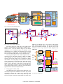
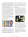
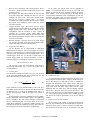
A Front-End DAQ with Buffer and Flexible Triggers
Y. Cui, member, IEEE, K.A. Lan, member, IEEE, E.V. Hungerford
Physics, University of Houston, Houston TX 77204
Abstract - The data acquisition architecture for the tracking
detector of the MECO experiment will consist of a
preamplifier/discriminator feeding a buffered digitizer which will
be controlled by programmed logic. The digitizer converts the
timing and analog waveform into digital storage for later readout.
In order to evaluate this conceptual design, a prototype system
was assembled using an existing digitizer chip, which had similar
characteristics to the one proposed for MECO. In this prototype
system, the event readout sequence and trigger was controlled by
a Xilinx FPGA, and gated data events were transferred for
further processing to higher levels in the data stream. The system
contained 64 input channels divided into 4 groups of 16 channels,
and either anode or cathode signals could be processed. It could
be operated in either an internal or external trigger mode.
Test results are reported in this paper, including the maximum
event rate, the system dead time, and the relationship between the
system efficiency and the hitmap selection. Based on these test
results, some improvements in the digitizer chip are discussed,
and the specifications of our proposed digitizer are presented.
Index Terms - Tracking Detector, DAQ System, FPGA, Digitizer,
Front-end.
I.
INTRODUCTION
A prototype, 64 channel DAQ system was built to prove
the design concept for reading out the MECO tracking detector
[1]. The challenges to the MECO DAQ system were reported
elsewhere [3]. These include not only the large number of
readout channels (24000), but also the experimental
environment as the detector itself is placed in a sealed vacuum
container and immersed in a high magnetic field). A front-end
system architecture, consisting of a preamplifier-discriminator
feeding a buffered digitizer which is controlled by
programmed logic, was proposed. The front-end would be
installed on the detector frame within the vacuum. In order to
evaluate the detector performance, several sets of straw
tracking detectors, and a prototype front-end system, were
built to clarify problems that might arise with this design. The
prototype was constructed using an existing digitizer chip from
the Babar experiment [4], which has similar characteristics to
our design. The system successfully worked with different
straw prototypes, under different environment conditions. Test
results of this prototype system are reported in this paper.
II. SYSTEM ARCHITECTURE
A. System Requirements and Architecture
A GEANT simulation [2] of the MECO experiment shows
that the tracking detector must operate at very high rate.
During the muon production period (0~600ns after a beam
pulse), the single event rate is about 10~15MHz per straw.
Although MECO will not acquire data during this period, the
system must recover for data acquisition after 600ns and
remain operational until the next beam pulse ~1350ns later.
The background rate during the data acquisition period is
500k/straw. The tracking accuracy, the 200µm azimuthal
resolution and 2mm axial resolution, needs an electronics
system having approximately 1ns TDC resolution and an 8-bit
ADC for the pulse waveform. In addition, one third of the
background events come from low energy protons which
deposit 20 times the energy of the signal electrons. Although
we are not interested in this ~5pC proton background, an
electron signal of ~200fC puts severe constraints on the
dynamic range of the system and system recovery after
saturation.
There are two methods to obtain the total charge
information. One uses a large integration time to collect the
charge in all clusters and measure the peak signal of the
waveform. However, the long tail reduces peak resolution in a
high rate environment.
Another method uses a small
integration time to smooth the cluster fluctuation, and
integrates the signal current waveform. This tolerates a much
higher rate for the same resolution, and it is used in our
system.
To satisfy the MECO requirements, the system consists of
four blocks, 1) Preamplifier Board (PB), 2) Analog Digitizer
Board (ADB), 3) Control Motherboard (CMB), and 4) Upper
level DAQ system including storage. A 64-channel system is
shown in Fig. 1.
B. Preamplifier Board (PB)
Each PB board has 16 input-channels, and is connected to
the detector by a short, custom-made flexible cable in order to
reduce radiation in the tracking volume. The detector signals
are pre-amplified and discriminated on this board. On each PB
board, four 4-channel ASD chips were used. These were
designed by KEK [5] for the ATLAS thin gap chamber. This
chip has a fast differential timing output and a single-ended
amplitude output (16ns integration time) for each channel.
0-7803-8701-5/04/$20.00 (C) 2004 IEEE
SPI Series Bus
4×(ASD-4)/FEB
PA
OPA
DAC
2×(Elefant)/ADB
Chip Select
Sh
Sh
Shaper
Shaper
Gain
L1_Accept
Dis
Dis
c.
Dis
8x2
PB
Straw Detector
Clock
60MHz
Trig Pattern
Trigger
Decision
4
ADB
Data
TXER
XC2S100-5PQ208C
Hit point
Multiplexer
(XCR3128-6VQ100C)
Ack
FPGA
SysClk
32
Vth
Data Bus
8
Level
Convert
c.
Disc.
c.
Readout
Sequencer
Address Bus
Elefant
Digitizer
16
Req
Data
Transmitter
Command
Receiver
(XCR3128)
16k FIFO
4×(ADB)/ CMB
Ext. trig. In
CMB
Fig 1. Structure of the Signal Readout System
R3 2k
R6
1k
16k
+3.3V
1p
Analog
output
R1
3.16k
+ OUT
5
6
Timing
output
C3 2.7p
11
1k
C6
C2
25p
1
2
R9
510
7
0
-IN
4
3
Out
+IN
14
R10 1k
6
U1A
-Vs DIS
OPA2690
0
11 +5V
20p
+5V
+Vs
C1
0.1u
- OUT
R2
+Vs
+IN
4
5
C7
0.1u
8
Out
R11-5V
1k
R7
100
R10 50
-IN
OUT
U1B
OPA2690
-Vs DIS
R8
100
0
0
+5V
-5V
+5V
ASD
Fig 2. Diagram of One Channel in PB Board
We made a PB for the anode and for the cathode signal
readout. The threshold of an anode PB is normally set at 100mV (25fC). Since the induced charge on the cathode
distributes on 3~5 continuous strips, the threshold of the
cathode PB is set at +300mV (75fC) allowing only the central
strip to produce a timing output. Accurate timing correlation
between anode and cathode helps to resolve multi-hit events.
An extra gain amplifier with 100ns integration time, is
connected to the ASD analog output to match the 15MHz
ADC sampling rate of the current ADB board. It is not
necessary for the final design to have a sampling rate higher
than 40MHz. The timing output of the PB board is connected
to the ADB board by a twisted-pair cable. Both short (1.5ft)
and long (10ft) cables have been tested, but for the analog
signal, we use a short piece of flat cable or a long multi-coax
cable. Similar cables can also be used to connect the PB board
to the CAMAC DAQ system. In all cases, we did not observe
significant noise due to the transmission lines.
C. Analog Digitizer Board (ADB)
The ADB board accepts signals from the PB boards. The
most important part of the ADB board is an ASIC chip, which
continuously digitizes the timing and waveform, and
temporarily stores the data in the on-chip buffer. Upon the
arrival of a trigger, the data are readout under the control of the
MB board. The Elefant chip [7] was selected as the digitizer
ASIC for the prototype system. This chip was successfully
used for the BaBar experiment [4] and has most of the
functions we need. Fig. 3 shows the block diagram of our
ADB board.
CS0
8
HFA3102
LVDS
OC
8
8
L1_Accept
ELEFANT
8 Amp
Digital
Input
8
8
1
Analog
Input
CS1
8
HFA3102
1
OC
8
8
RD_Add
ELEFANT
WR_Add
8 Amp
8
8
8
Vth, Vref
DAC
& Driver
LD
SPI
Fig 3. Diagram of ADB Board
0-7803-8701-5/04/$20.00 (C) 2004 IEEE
8
8
CPLD
DAT
Reset
SysClk
Trig_pattern
CS2 4
SPI
JTAG
The ADB outputs are processed further on this board to
satisfy the input requirements of the Elefant ASIC. For digital
signals, LVDS signals are converted to the open collector (OC)
signals by differential pairs HFA3102. Actually, this circuit
can also convert ECL or NIM signal into OC signals by
changing the DC operating voltage. For analog inputs, single
ended signals are converted to differential signals, and at the
same time, the gain is also adjusted. The electronics also
allows different input polarities to be selected.
The Elefant chip can produce a output “triggered” signal
for each channel in every time slice when a TDC signal is
present or the slope of a waveform is larger than a preassigned value. Using this signal, a Xilinx CoolRunner
XPLA3 CPLD encodes a 16-bit “trigger” signal (one bit for
each of 16 channels) into a 4-bit trigger pattern output. This
pattern can be used by the CMB board to help make an L1
decision. When a valid trigger is presented, data is readout
from the Elefant chip into the CMB board.
There is also Serial Peripheral Interface (SPI) decoder
logic in this CPLD. It receives the SPI commands from the
CM board to control the gain of the amplifier in the Elefant
chip and set the DAC values. The DAC provides the
thresholds to the ASD chips and reference voltages to the
Elefant chips. The former can change from -500mV to
500mV, while the later can vary from 0V to 4V.
Four ADB boards can feed a CMB board through a 96-pin
connector. The DACs on each ADB board can be set
individually, however, the number of ADB boards controlled
by one CMB is not limited to 4, and can be expanded
depending on the total readout rate on the bus.
Generator. All the system clocks to the devices are buffered
by a clock driver, and synchronized by the DLL circuit in the
FPGA.
For the prototype, the upper level system is a PC with a NI
6534 DIO PCI interface card. A program written in LabView
is used to control the data processing. In the final detector
system, the upper level system will be a high level event
builder.
1) ROC FPGA Design
The ROC FPGA design is the most important part of system. It
has the following functions:
∗ At power on, The ROC generates a RESET signal to
initialize the whole system to a known state. After that,
the ROC generates a SYNC signal periodically to
synchronize the TDC counters in all the Elefant chips.
∗ During a run, when a coincident event occurs, ROC
generates a delayed L1_Accept signal. This delay is
needed by the latency buffer (12.6us latency time) in the
Elefant chip to access the appropriate data.
∗ After generating the L1_Accept, the ROC waits for data
of the current event to be moved from the latency buffer to
the event buffer (about 2.2us). In this period, the ROC is
dead to a new coincident event.
Sync Reset
Run
SysClk
L1_Accept
D. Control Motherboard (CMB)
Trigger
pattern
FS & CS
SD
SC
Sync
Reset
Mode
6
CS
8
RD_Addr
2
WR_Addr
2
Buff_Sel
3
Data
8
L1_Accept
Trig_Pattern
8
Ext Trig
2
SysClk
Q 16
FDATA 16
WClk
WEn
RClk
REn
Readout
Controller
FPGA
FIFO
TXer
Ack
Req
Data
16
Ack
Req
Cmd
16
OSC Clock
60MHz
DLL
Config
OSC
&
Clock
Generation
FLASH
PROM
JTAG
Fig 4. Diagram of CMB Board
The CMB board diagram is shown in Fig. 4. A Xilinx
Spartan-II FPGA is used as the readout controller (ROC) to
make the trigger decision and generate the L1_Accept signal.
The data from ADB are then build into a sub-event package.
A 32k byte TI FIFO is used for buffering data. A Xilinx
CoolRunner XPLA3 CPLD works as a transceiver (TXer) to
interface the upper level DAQ system. In addition, there is a
flash PROM containing the configuration data of the FPGA, a
JTAG chain for in-system programming, and a Clock
Start / Stop
SPI
Run Control
Reset & Sync
Generation
Clk15
Generation
Trigger
Decision Making
Logic Control
clk1
Readout
Sequence
Control Logic
Data to
FIFO
8
16
stop
start
WR Buf
RD Buf
16
2
External Trigger Wr_addr
2
8 Data from Elefant
Rd_addr Vth, Sel, CS
Fig 5. FPGA logic for the Readout Controller
∗
∗
After data transfer, the ROC starts a readout process to
read data from Elefant (with or without zero suppression),
build an event data frame, and write it to the FIFO.
If there is a new event during the readout process, the
ROC temporarily saves the appropriate event flag in a
buffer. When the current readout completes, the ROC
starts a new process to readout this saved event. Because
there are only four event buffers in the Elefant chip, there
are at most 3 events waiting for readout.
In order to implement these functions, this ROC FPGA
has the structure in Fig. 5. It has five function blocks.
∗ Clk15 Generation. This provides 15MHz clock to other
blocks in FPGA. It uses the same circuit as the one in the
Elefant chip to synchronize the working frequency with
the Elefant chips. In this way, all the clk15 signals in the
system synchronized.
0-7803-8701-5/04/$20.00 (C) 2004 IEEE
∗
∗
∗
∗
Reset & Sync Generation. This block generates ‘Reset’
and ‘Sync’, which synchronize all the logic devices in the
prototype system.
Run Control. This logic block controls the run start and
stop when taking data. Through the SPI bus, one can
configure the preset event / preset time counting mode,
and set the respective register value.
A counter
accumulates the event recorded or the time elapsed. When
the counter value reaches the register value, the current
run will be stopped.
Trigger Decision Logic. This block receives trigger
signals from the Elefant chips in the system and external
trigger signals from other detectors. Based on the
configuration and the assertion of these signals, it
generates an L1_Accept signal, which starts data
movement from the latency buffer to the event buffer, and
also enables the Readout Sequence block to readout this
event after a time delay.
Readout Sequence. Upon the arrival of an event trigger
(L1_Accept), this block reads data from the Elefant chip,
build a data frame, and write it into the FIFO.
In the future, the system clock will be upgraded to
40MHz. For 60 channels with 16 time slices in an event, and
10 bits for each time slice, the estimated counting rate will be
about 100kHz. If we do preprocessing in the ROC FPGA,
such as baseline subtraction, ADC compensation, or peak area
calculation, the output event size can be decreased by a factor
of 3 or 4, and higher counting rates can be obtained.
E. Trigger Decision Making
An L1 decision can be programmed to implement
different decision strategies, such as a self-trigger, an externaltrigger, or a coincident trigger. In the self-trigger mode, an L1
decision is made on a pattern on internal trigger signals. In an
external-trigger mode, the L1 decision is made when an
external trigger signal, e.g. from the calorimeter, is valid. A
coincident trigger is a combination of the above two modes.
III. PERFORMANCE TEST
The prototype system was tested and its performance is
discussed in this section. Fig. 6 shows the system with a
vacuum chamber.
A. Counting Rate
The maximum counting rate of the system (fmax Hz) depends
on the speed that buffered data can be transferred into and
moved from the FIFO, as shown in Equ. 1.
f max = min(
f
fbus
, sys )
N ch * NT * B NT
(1)
In this equation, Nch is the channel number of an event, NT is
the number of time slices to be readout, B is data width in bits
of each time slice, fsys in Hz is the sampling clock, and fbus is
the bus speed from the CMB to the upper level system in
bits/s.
In our prototype system, the sampling clock was 15MHz,
and the parallel bus from the CMB to the PC was 10MHz by
16 bits (160Mb/s). We used a pulse generator to feed signal
into 16 channels and read out 16 time slices for an event.
Under these conditions, we reached a 60kHz counting rate,
somewhat lower than the estimation of Equ.(1) due to the low
processing speed of the PC and LabView programming.
Fig 6. The Whole Prototype System
B. Double Pulse Test
An experiment was designed to check the waveform of the
charge integration from the ASIC. Single or double pulses are
sent to the input of an ASD chip in order to emulate the
irregular time distribution of the cluster charge. The pulse
width is 15ns, and the double pulse separation is 30ns. Two
scope plots show the input signal (ch4) and the output
amplitude from the ASD (ch2), and the shaping amplifier
output (ch3). The peak values are 251mV and 151mV. The
sum of 8 time slices from waveform digitizer output is 92 and
47. This signal processing method, with a 40MHz upgrade,
will satisfy the required performance level for the MECO
readout.
C. Events lost due to TDC deadtime
All the analog input signals are digitized and buffered.
However, the internal logic of the Elefant digitizer requires at
least three clock cycles (3×66ns) to read the next TDC data.
This means that if two hits occur in one channel in less than
0-7803-8701-5/04/$20.00 (C) 2004 IEEE
200ns, a pileup waveform will occur, but the timing of the
second event is lost. The clock rate in the new MECO
digitizer will be 40MHz to reduce this effect.
Where n is the trigger rate, τ is the deadtime (128µs), and
m=4 for the Elefant chip buffers. If the trigger rate is 10kHz,
this gives a 3.1% data lost. Thus a sparse readout and fewer
number of time slices must be used.
All the above
requirements will be considered in the upgrade chip design.
IV. CONCLUSION
This paper describes the architecture of a data acquisition
system for the MECO tracking detector. The prototype system
has been designed using the Xilinx Spartan-II FPGA,
CoolRunner XPLA3 CPLD and sample Elefant chips. This
prototype verifies the Amplifier-Digitizer-Readout Logic
system structure proposed for MECO will work as designed,
although the proposed system must use a higher clock rate, and
have several other features re-engineered.
We anticipate that the flexibility designed into the new
system will provide many opportunities to implement it in
other high count rate environments.
V. ACKNOWLEDGMENT
This work is partly supported by the NSF and DOE. The
authors acknowledge H. Von der Lippe from LBNL, who
supplied the Elefant chips for our prototype and preparing
upgrade chip design. Thanks also go to M. Kelsey from
SLAC, BaBar Chamber group. A fruitful discussion with him
helps to solve the problems in using the Elefant chip in our
system design.
Reference
Fig. 7. The double pulse waveform of PB board
D. Events lost due to the latency buffer
When a trigger initiates a data read, the buffered 32 time
slices of data are moved into event buffers within 2.11µs
(32×66ns). Another trigger cannot initiate another read during
this period, and this also produces dead-time. The percentage
of the lost events equals the trigger rate times this dead-time.
As discussed in a previous paper [3], the proposed upgrade to
the Elefant chip will solve this problem.
[1]. MECO [Online]. Available: http://meco.ps.uci.edu/
[2]. MECO collaboration, "Draft MECO Technical Proposal",
Chapter 9.3, [Online]. Available: http://meco.ps.uci.edu/.
[3]. K. Lan, "A Pipelined Front-end, Timing and Amplitude
Digitizing System", IEEE Trans. Nucl. Sci., vol. 51, Oct.
2004.
[4]. BaBar Experiment, [online]
http://www.slac.stanford.edu/BFROOT/www/Detector/Ce
ntralTracker/index.html.
[5]. Sasaki and M. Yoshiro, "ASD IC for thin gap chamber in
the LHC ATLAS experiment," IEEE Trans. Nucl. Sci.,
vol. 46, pp. 1871-1875, Dec. 1999.
[6]. Natianal Instruments, DAQ 653X User Manual. [Online].
Available: http://ni.com/
[7]. Scott Dow, et al., "Design and Performance of the Elefant
Digitizer IC for the BaBar Drift Chamber", IEEE Trans.
Nucl. Sci., vol. 46, pp 785-792, Aug. 1999.
E. Events lost due to the control system
There are four event buffers in an Elefant chip. When
they are all occupied, the system halts further triggers. The
readout time for a non-sparse readout of all 64 channels, each
having a 32 time slices waveform, is 128µs. The data lost due
to this can be calculated by the Poisson distribution;
(nτ ) m − nτ
Pm (nτ ) =
e
m!
(2)
0-7803-8701-5/04/$20.00 (C) 2004 IEEE