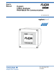
1
User’s Manual FLXA21 2-Wire Analyzer FOUNDATION Fieldbus Communication IM 12A01A02-71E IM 12A01A02-71E 2nd Edition i uIntroduction Thank you for purchasing the FLXA21 2-Wire Analyzer. Please read the following respective documents before installing and using the FLXA21. This manual describes only those topics that are required for operation of the FOUNDATION Fieldbus communications. For information about the FLXA21 other than FOUNDATION Fieldbus, refer to the User’s Manual (IM 12A01A02-01E). n Notes on Handling User’s Manuals • Please hand over the user’s manuals to your end users so that they can keep the user’s manuals on hand for convenient reference. • Please read the information thoroughly before using the product. • The purpose of these user’s manuals is not to warrant that the product is well suited to any particular purpose but rather to describe the functional details of the product. • No part of the user’s manuals may be transferred or reproduced without prior written consent from YOKOGAWA. • YOKOGAWA reserves the right to make improvements in the user’s manuals and product at any time, without notice or obligation. • If you have any questions, or you find mistakes or omissions in the user’s manuals, please contact our sales representative or your local distributor. n Drawing Conventions Some drawings may be partially emphasized, simplified, or omitted, for the convenience of description. Some screen images depicted in the user’s manual may have different display positions or character types (e.g., the upper / lower case). Also note that some of the images contained in this user’s manual are display examples. n Model Name used in this Manual The model names, FLXA21-PH and FLXA21-SC, are used in this manual. The FLXA21-PH means the FLXA21 with the output of FOUNDATION Fieldbus communication and with measurement of pH and/or ORP. The exact model & style code is as follows; FLXA21-D-P-D-AA-P1-NN-F-N-LA-N-NN (1st input: pH/ORP) or FLXA21-D-P-D-AA-S1-NN-F-N-LA-N-NN (1st input: pH/ORP (SENCOM sensor)) And, the FLXA21-SC means the FLXA21 with the output of FOUNDATION Fieldbus communication and with measurement of conductivity. The exact model & style code is as follows; FLXA21-D-P-D-AA-C1-NN-F-N-LA-N-NN (1st input: Conductivity (SC)) Media No. IM 12A01A02-71E 2nd Edition : Oct. 2015 (YK) All Rights Reserved Copyright © 2015, Yokogawa Electric Corporation IM 12A01A02-71E 2nd Edition : Oct. 01, 2015-00 ii u Safety Precautions n Safety, Protection, and Modification of the Product • In order to protect the system controlled by the product and the product itself and ensure safe operation, observe the safety precautions described in this user’s manual. We assume no liability for safety if users fail to observe these instructions when operating the product. • If this instrument is used in a manner not specified in this user’s manual, the protection provided by this instrument may be impaired. • If any protection or safety circuit is required for the system controlled by the product or for the product itself, prepare it separately. • Be sure to use the spare parts approved by Yokogawa Electric Corporation (hereafter simply referred to as YOKOGAWA) when replacing parts or consumables. • Modification of the product is strictly prohibited. • The following words are used this manual. CAUTION This symbol gives information essential for understanding the operations and functions. NOTE This symbol indicates information that complements the present topic. n Warning and Disclaimer The product is provided on an “as is” basis. YOKOGAWA shall have neither liability nor responsibility to any person or entity with respect to any direct or indirect loss or damage arising from using the product or any defect of the product that YOKOGAWA can not predict in advance. IM 12A01A02-71E 2nd Edition : Oct. 01, 2015-00 iii nFLXA21 • The FLXA21 should only be used with equipment that meets the relevant IEC, American, Canadian, and Japanese standards. Yokogawa accepts no responsibility for the misuse of this unit. • Don’t install “general purpose type” instruments in the hazardous area. • The Instrument is packed carefully with shock absorbing materials, nevertheless, the instrument may be damaged or broken if subjected to strong shock, such as if the instrument is dropped. Handle with care. CAUTION Electrostatic discharge The FLXA21 contains devices that can be damaged by electrostatic discharge. When servicing this equipment, please observe proper procedures to prevent such damage. Replacement components should be shipped in conductive packaging. Repair work should be done at grounded workstations using grounded soldering irons and wrist straps to avoid electrostatic discharge. CAUTION • • Do not use an abrasive or organic solvent in cleaning the instrument. Substitution of components may impair suitability for Division 2. Do not remove or replace while circuit is live unless area is known to be non-hazardous. Explosion Hazard – Do not disconnect equipment unless area is known to be nonhazardous. Do not reset circuit breaker unless power has been removed from the equipment or the area is known to be non-hazardous. • This instrument is a EN61326-1 Class A product, and it is designed for use in the industrial environment. Please use this instrument in the industrial environment only. l How to dispose the batteries: This is an explanation about the new EU Battery Directive(DIRECTIVE 2006/66/EC).This directive is only valid in the EU. Batteries are included in this product.Batteries incorporated into this product cannot be removed by yourself.Dispose them together with this product. When you dispose this product in the EU,contact your local Yokogawa Europe B.V.office.Do not dispose them as domestic household waste. Battery type: Manganese dioxide lithium battery Notice: The symbol means they shall be sorted out and collected as ordained in ANNEX II in DIRECTIVE 2006/66/EC. IM 12A01A02-71E 2nd Edition : Oct. 01, 2015-00 iv l Regulatory Compliance Safety: UL 61010-1 UL 61010-2-030 CAN/CSA C22.2 No.61010-1 CAN/CSA-C22.2 No.61010-2-030 EMC:EN61326-1 Class A, Table 2 (For use in industrial locations) Influence of immunity environment (Criteria A): ±25% of F.S. EN61326-2-3 EN61326-2-5 AS/NZS CISPR11 Korea Electromagnetic Conformity Standard Class A 한국 전자파적합성 기준 A급 기기 (업무용 방송통신기자재) 이 기기는 업무용(A급) 전자파적합기기로서 판매자 또는 사용자는 이 점을 주의하시기 바라며, 가정외의 지역에서 사용하는 것을 목적으로 합니다. Installation altitude: 2000 m or less Category based on IEC 61010: I (Note 1) Pollution degree based on IEC 61010: 2 (Note 2) Note 1: Installation category, called over-voltage category, specifies impulse withstand voltage. Equipment with “Category I” (ex. two-wire transmitter) is used for connection to circuits in which measures are taken to limit transient over-voltages to an appropriately low level. Note 2: Pollution degree indicates the degree of existence of solid, liquid, gas or other inclusions which may reduce dielectric strength. Degree 2 is the normal indoor environment. n Warranty and service Yokogawa products and parts are guaranteed free from defects in workmanship and material under normal use and service for a period of (typically) 12 months from the date of shipment from the manufacturer. Individual sales organisations can deviate from the typical warranty period, and the conditions of sale relating to the original purchase order should be consulted. Damage caused by wear and tear, inadequate maintenance, corrosion, or by the effects of chemical processes are excluded from this warranty coverage. In the event of warranty claim, the defective goods should be sent (freight paid) to the service department of the relevant sales organisation for repair or replacement (at Yokogawa discretion). The following information must be included in the letter accompanying the returned goods: • • • • • • • Part number, model code and serial number Original purchase order and date Length of time in service and a description of the process Description of the fault, and the circumstances of failure Process/environmental conditions that may be related to the failure of the device. A statement whether warranty or nonwarranty service is requested Complete shipping and billing instructions for return of material, plus the name and phone number of a contact person who can be reached for further information. Returned goods that have been in contact with process fluids must be decontaminated/ disinfected before shipment. Goods should carry a certificate to this effect, for the health and safety of our employees. Material safety data sheets should also be included for all components of the processes to which the equipment has been exposed. IM 12A01A02-71E 2nd Edition : Oct. 01, 2015-00 v n Copyright and Trademark Notices The copyrights of online manual contained in the CD-ROM are reserved. The online manual is protected by the PDF security from modification, however, it can be output via a printer. Printing out the online manual is only allowed for the purpose of using the product. When using the printed information of the online manual, check if the version is the most recent one by referring to the CD-ROM’s version. No part of the online manual may be transferred, sold, distributed (including delivery via a commercial PC network or the like), or registered or recorded on video tapes. FLEXA, FLXA and SENCOM are registered trademarks of Yokogawa Electric Corporation. Adobe, Acrobat and Acrobat Reader are either registered trademarks or trademarks of Adobe Systems Incorporated in the United States and/or other countries. All other company and product names mentioned in this user’s manual are trademarks or registered trademarks of their respective companies. We do not use TM or ® mark to indicate those trademarks or registered trademarks in this user’s manual. l FLXA21’s fonts (c) Copyright 2000-2001 /efont/ The Electronic Font Open Laboratory. All rights reserved. Redistribution and use in source and binary forms, with or without modification, are permitted provided that the following conditions are met: 1. Redistributions of source code must retain the above copyright notice, this list of conditions and the following disclaimer. 2. Redistributions in binary form must reproduce the above copyright notice, this list of conditions and the following disclaimer in the documentation and/or other materials provided with the distribution. 3. Neither the name of the team nor the names of its contributors may be used to endorse or promote products derived from this font without specific prior written permission. THIS FONT IS PROVIDED BY THE TEAM AND CONTRIBUTORS “AS IS” AND ANY EXPRESS OR IMPLIED WARRANTIES, INCLUDING, BUT NOT LIMITED TO, THE IMPLIED WARRANTIES OF MERCHANTABILITY AND FITNESS FOR A PARTICULAR PURPOSE ARE DISCLAIMED. IN NO EVENT SHALL THE TEAM OR CONTRIBUTORS BE LIABLE FOR ANY DIRECT, INDIRECT, INCIDENTAL, SPECIAL, EXEMPLARY, OR CONSEQUENTIAL DAMAGES (INCLUDING, BUT NOT LIMITED TO, PROCUREMENT OF SUBSTITUTE GOODS OR SERVICES; LOSS OF USE, DATA, OR PROFITS; OR BUSINESS INTERRUPTION) HOWEVER CAUSED AND ON ANY THEORY OF LIABILITY, WHETHER IN CONTRACT, STRICT LIABILITY, OR TORT (INCLUDING NEGLIGENCE OR OTHERWISE) ARISING IN ANY WAY OUT OF THE USE OF THIS FONT, EVEN IF ADVISED OF THE POSSIBILITY OF SUCH DAMAGE. IM 12A01A02-71E 2nd Edition : Oct. 01, 2015-00 Toc-1 FLXA21 2-Wire Analyzer FOUNDATION Fieldbus Communication IM 12A01A02-71E 2nd Edition CONTENTS uIntroduction.....................................................................................................i u Safety Precautions........................................................................................ii 1. About FOUNDATION Fieldbus................................................................. 1-1 1.1 Internal Structure of FLXA21............................................................................ 1-1 1.2 Logical Structure of Each BLOCK................................................................... 1-2 1.3 Wiring System Configuration........................................................................... 1-2 2.Preparation................................................................................................. 2-1 3. 4. 2.1 Cables, terminals and glands for FOUNDATION Fieldbus............................ 2-1 2.2 Shielding and grounding.................................................................................. 2-3 2.3 How to download DD for CFF........................................................................... 2-3 Getting started........................................................................................... 3-1 3.1 Connection of Devices...................................................................................... 3-1 3.2 Host Setting........................................................................................................ 3-2 3.3 Bus Power ON.................................................................................................... 3-3 3.4 Integration of DD................................................................................................ 3-3 3.5 Set the parameters using DTM......................................................................... 3-3 3.6 Reading the Parameters.................................................................................... 3-4 3.7 Continuous Record of Values........................................................................... 3-4 3.8 Generation of Alarm........................................................................................... 3-4 3.9 PRIMARY/SECONDARY/TERTIARY/QUATERNARY_VALUE Value Assignment..... 3-4 Configuration............................................................................................. 4-1 4.1 Network Design.................................................................................................. 4-1 4.2 Network Definition............................................................................................. 4-2 4.3 Definition of Combining Function Blocks....................................................... 4-3 4.4 Setting of Tags and Addresses........................................................................ 4-4 4.5 Communication Setting.................................................................................... 4-5 4.6 5. 4.5.1 VCR Setting........................................................................................ 4-5 4.5.2 Function Block Execution Control....................................................... 4-8 Block Setting...................................................................................................... 4-8 4.6.1 Link Object.......................................................................................... 4-8 4.6.2 Trend Object....................................................................................... 4-8 4.6.3 View Object......................................................................................... 4-9 Explanation of Basic Items...................................................................... 5-1 IM 12A01A02-71E 2nd Edition : Oct. 01, 2015-00 Toc-2 5.1 AI Function Block............................................................................................... 5-1 5.1.1 Function Blocks................................................................................... 5-1 5.1.2 MODE_BLK........................................................................................ 5-1 5.1.3 CHANNEL........................................................................................... 5-2 5.1.4XD_SCALE/OUT_SCALE.................................................................. 5-2 5.1.5L_TYPE............................................................................................... 5-3 5.1.6 PV_FTIME.......................................................................................... 5-3 5.1.7 Alarm Priority....................................................................................... 5-3 5.1.8 Alarm Threshold.................................................................................. 5-3 5.1.9IO_OPTS............................................................................................ 5-3 5.1.10STATUS_OPT..................................................................................... 5-4 5.2 6. 7. 8. Sensor Transducer Block................................................................................. 5-4 5.2.1 MODE_BLK........................................................................................ 5-4 5.2.2 BLOCK_ERR...................................................................................... 5-5 5.2.3 XD_ERROR........................................................................................ 5-5 In-process operation................................................................................. 6-1 6.1 Mode Transition................................................................................................. 6-1 6.2 Generation of Alarm........................................................................................... 6-1 6.3 Simulation Function.......................................................................................... 6-4 6.4 Write lock (Write-protect) function................................................................... 6-4 List of parameters for each block of the FLXA21.................................. 7-1 7.1 Resource Block.................................................................................................. 7-2 7.2 Analog input Block............................................................................................ 7-9 7.3 Sensor Transducer Block............................................................................... 7-12 Diagnostic Information............................................................................. 8-1 8.1 DEVICE STATUS................................................................................................. 8-1 8.2 Status of each parameter in failure mode FLXA21-PH................................ 8-14 8.3 Status of each parameter in failure mode FLXA21-SC................................ 8-21 Appendix 1 Link Master Functions........................................................ App.1-1 Appendix 2 Software Download............................................................. App.2-1 Revision Record........................................................................................................i IM 12A01A02-71E 2nd Edition : Oct. 01, 2015-00 1. 1-1 <1. About FOUNDATION Fieldbus> About FOUNDATION Fieldbus FOUNDATION Fieldbus is a bi-directional digital communication protocol for field devices, which offers an advancement implementation technologies for process control systems and is widely employed by numerous field devices. FLXA21 FOUNDATION Fieldbus communication type employs the specification standardized by The FOUNDATION Fieldbus, and provides interoperability between Yokogawa devices and those produced by other manufacturers. FOUNDATION Fieldbus comes with software consisting of three AI function blocks, providing the means to implement flexible instrumentation system. For information on other features, engineering, design, construction work, startup and maintenance of FOUNDATION Fieldbus, refer to http://www.yokogawa.com/fbs/fbs-index.htm. 1.1 Internal Structure of FLXA21 The FLXA21 contains two virtual field devices (VFD) that share the following functions. n System/network Management VFD • Sets node addresses and Physical Device tags (PD Tag) necessary for communication • Controls the execution of function blocks • Manages operation parameters and communication resources (Virtual Communication Relationship: VCR) n Function Block VFD l Resource block • Manages the status of FLXA21 hardware • Automatically informs the host of any detected faults or other problems l Sensor Transducer block • Converts sensor output to process values and transfers to AI function block by channels l AI1, AI2, AI3 function block • Conditions raw data from the Sensor Transducer block • Outputs conditioned process values • Carries out scaling, damping and square root extraction IM 12A01A02-71E 2nd Edition : Oct. 01, 2015-00 1-2 <1. About FOUNDATION Fieldbus> 1.2 Logical Structure of Each BLOCK System/network management VFD PD Tag Node address Communication parameters VCR Function block execution schedule Sensor Function block VFD Sensor input SENSOR Transducer block AI function block AI function block AI function block Block tag Block tag Parameters Parameters Output OUT Resource block Block tag Parameters Figure 1.1 Logical Structure of Each Block Setting of various parameters, node addresses, and PD Tags shown in Figure 1.1 is required before starting operation. 1.3 Wiring System Configuration The number of devices that can be connected to a single bus and the cable length vary depending on system design. When constructing systems, both the basic and overall design must be carefully considered to allow device performance to be fully exhibited. IM 12A01A02-71E 2nd Edition : Oct. 01, 2015-00 2-1 <2. Preparation> 2.Preparation The FLXA21 FOUNDATION Fieldbus is provided with three cable glands. The first is used for the electrode wiring as the other is used for the power wiring shown in Figure 2.1. For sensor cable For power supply For grounding cable Figure 2.1 2.1 Cable gland diagram Cables, terminals and glands for FOUNDATION Fieldbus Wire and install the system by referring to chapter 2 in the FLXA21 instruction manual (IM 12A01A02-01E). The FOUNDATION Fieldbus power supply is 9 to 32 V DC. The wiring is the same. However, for the FOUNDATION Fieldbus cables, see Table 2.1. Table 2.1 FOUNDATION Fieldbus Cables and transmissible Length Parameters Max DC Resistance, Ω/km Max Attenuation, dB/km Conditions per conductor 1.25 f, (39 kHz) Gauge — Max Length, meters — Type A 22 3.0 #18 AWG (0.82 mm2) 1,900 Type B 56 5.0 #22 AWG (0.32 mm2) 1,200 Type C 132 8.0 #26 AWG (0.13 mm2) 400 Type D 20 8.0 #16 AWG (1.25 mm2) 200 IM 12A01A02-71E 2nd Edition : Oct. 01, 2015-00 Note: 1900 m is trunk + sum of Spurs (Max length type A cable) Yokogawa recommends the use of Type A. Usage of Type B and D is restricted. Yokogawa does not recommend the use of Type C. Table 2.2 Recommended length of Spur Cables Number of spur cables 15-16 13-14 1-12 Length of a non-intrinsically safe spur cable 60 m 90 m 120 m Note: • 1 device per spur. • Keep as short as possible (min 1 m) 2-2 <2. Preparation> l When using a SENCOM module When using a SENCOM module, you need to use the supplied cable clamp to fix the sensor cables in place. Attach the supplied cable clamp as shown in Figure 2.2. Sensor cable Cable cramp Figure 2.2 When using a SENCOM module l DIP switches Figure 2.3 shows the DIP switches for setting the address and write protection. Normally, you do not have the change them from the default settings. Write protection switch (Default: OFF) ON OFF Address switch (Default: Hardware address is disabled) ON OFF 7 6 5 4 3 2 1 0 Figure 2.3 DIP switches IM 12A01A02-71E 2nd Edition : Oct. 01, 2015-00 2.2 <2. Preparation> 2-3 Shielding and grounding Grounding and shielding of FLXA21 is necessary for a safe and reliable operation. Please use one of the following schemes (A or B) as these will give proper shielding and grounding. One should pay special attention to instruments that required an external power supply (besides the 9 to 32 V supplied by the bus). V4 A Spur trunck cable Power unit FLXA21 Junction box V1 Spur Field device V3 V2 V1 = V2 = V3 = V4 Potential equalisation line (German practice) B Power unit Spur trunck cable FLXA21 Junction box Spur Field device High integrity earth, 0.1R or better Neutral star-point bonding (English practice) Figure 2.4 2.3 Shield and grounding How to download DD for CFF If you do not have the DD or Capability file (CFF) files, you can download them from our web site. http://www.yokogawa.com/an/download/an-dl-fieldbus-001en.htm *: This address is subject to change without prior notice. If the above address cannot be accessed, consult your nearest sales office or the agency from which you purchased the product. IM 12A01A02-71E 2nd Edition : Oct. 01, 2015-00 3. 3-1 <3. Getting started> Getting started FOUNDATION Fieldbus is fully dependent upon digital communication protocol and differs in operation from conventional 4 to 20 mA transmission communication protocol. It is recommended that novice users use field devices in accordance with the procedures described in this section. The procedures assume that field devices will be set up on a bench or an instrument shop. 3.1 Connection of Devices The following instruments are required for use with FOUNDATION Fieldbus devices: • Power supply FOUNDATION Fieldbus requires a dedicated power supply. It is recommended that current capacity be well over the total value of the maximum current consumed by all devices (including the host). Conventional DC current cannot be used as is. • Terminator FOUNDATION Fieldbus requires two terminators. Refer to the supplier for details of terminators that are attached to the host. • Field devices Connect FLXA21 FOUNDATION Fieldbus communication type. Two or more FLXA21 devices or other devices can be connected. • Host Used for accessing field devices. A dedicated host (such as DCS) is used for an instrumentation line while dedicated communication tools are used for experimental purposes. For operation of the host, refer to the instruction manual for each host. No details of the host are explained in the rest of this material. • Cable Used for connecting devices. Refer to “Fieldbus Technical Information” (TI 38K03A01-01E) for details of instrumentation cabling. FOUNDATION Fieldbus uses twisted pair wires. To meet the Electro Magnetic Interference standards a shielded twisted pair is obligated. Refer to Yokogawa when making arrangements to purchase the recommended equipment. Connect the devices as shown in Figure 3.1. Connect the terminators at both ends of the trunk, with a minimum length of the spur laid for connection. The polarity of signal and power must be maintained. Fieldbus power supply Terminator HOST Terminator Terminator Figure 3.1 Cabling NOTE Before using a FOUNDATION Fieldbus configuration tool other than the existing host, confirm it does not affect the loop functionality in which all devices are already installed in operation. Disconnect the relevant control loop from the bus if necessary. IM 12A01A02-71E 2nd Edition : Oct. 01, 2015-00 3-2 <3. Getting started> CAUTION Connecting a FOUNDATION Fieldbus configuration tool to a loop with its existing host may cause communication data scrambles resulting in a functional disorder or a system failure. 3.2 Host Setting To activate FOUNDATION Fieldbus, the following settings are required for the host. CAUTION Do not turn off the power immediately after setting. When the parameters are saved to the EEPROM, the redundant processing is executed for an improvement of reliability. If the power is turned off within 60 seconds after setting is made, the modified parameters are not saved and the settings may return to the original values. Table 3.1 Symbol V (ST) V (MID) V (MRD) V (FUN) V (NUN) Operation Parameters Description and Settings Indicates the time necessary for immediate reply of the device. Unit of time is in octets (256 μs). Set maximum specification for all devices. For FLXA21, set a value of 4 or greater. Minimum-Inter-PDU-Delay Minimum value of communication data intervals. Unit of time is in octets (256 μs). Set the maximum specification for all devices. For FLXA21, set a value of 4 or greater. Maximum-Response-Delay The worst case time elapsed until a reply is recorded. The unit is Slot-time; set the value so that V (MRD) × V (ST) is the maximum value of the specification for all devices. For FLXA21, the setting must be a value of 12 or greater. First-Unpolled-Node Define the first address that can be used by the host. Set 0x15 or greater. Number-of-consecutive-Unpolled-Node This sets the number of consecutive unpolled nodes. FLXA21 address is factory-set to 0xEB. Set this address to be within the range of the BASIC device in Figure 3.5. Slot-Time 0x00 0x0F 0x10 0x13 0x14 V (FUN) Parameter Not used Bridge device LM device Not used V (FUN) + V (NUN) FLXA21 0xF7 0xF8 0xFB 0xFC 0xFF V (NUN) Basic device Default address Portable-device address Note 1: LM device: with bus control function (Link Master function) Note 2: BASIC device: without bus control function Figure 3.2 Available Address Range IM 12A01A02-71E 2nd Edition : Oct. 01, 2015-00 3.3 3-3 <3. Getting started> Bus Power ON Turn on the power of the host and the bus. First all segments of the display are lit, then the display begins to operate. If the indicator is not lit, check the polarity of the power supply. Using the host device display function, check that the FLXA21 is in operation on the bus. Unless otherwise specified, the following settings are in effect when shipped from the factory. Table 3.2 PD tag Node addr. DEV_TYPE FLXA21-PH PH1001 232 0x0402 FLXA21-SC SC1001 233 0x0403 If no FLXA21 is detected, check the available address range and the polarity of the power supply. If the node address and PD tag are not specified when ordering, default value is factory set. If two or more FLXA21’s are connected at a time with default value, only one FLXA21 will be detected from the host as FLXA21’s have the same initial address. Separately connect each FLXA21 and set a different address for each. 3.4 3.5 Integration of DD If the host supports DD (Device Description), the DD of the FLXA21 needs to be installed. Check if host has the following directory under its default DD directory. 594543\DEV_TYPE (594543 is the manufacturer number of Yokogawa Electric Corporation, and DEV_TYPE is the FLXA21 device number, respectively. Refer to Table 3.2.) If this directory is not found, DD of FLXA21 has not been included. Create the above directory and copy the DD file (0m0n.ffo,0m0n.sym) (m, n is a numeral) (to be supplied separately) into the directory. Once the DD is installed in the directory, the name and attribute of all parameters of the FLXA21 are displayed. Off-line configuration is possible by using Capability file (CFF). Set the parameters using DTM When configure the parameters using FieldMate, use the DTM (Device Type Manager) shown in the Table 3.3. Table 3.3 DTM Name DTM Model Name FLXA21-PH FLEXA FF DTM FLXA21-SC Analyzers DeviceType DeviceRevision 0x0402 1 0x0403 1 “Field Diagnostics” function (refer to IM 01R01A15-01EN) is available on FLXA21-PH or FLXA21-SC DTM Revision 3.4.0.21 or later. The DTM corresponding to the above is included in Yokogawa Device DTM Library 5.2/Device Files R 3.5.2.8 or later. IM 12A01A02-71E 2nd Edition : Oct. 01, 2015-00 3.6 3.7 3.8 3-4 <3. Getting started> Reading the Parameters To read FLXA21 parameters, select the AI1 block of the FLXA21 from the host screen and read the OUT parameter. The current process value is displayed. Check that MODE_BLOCK of the function block and resource block is set to AUTO, and change the signal input and read the parameter again. A new designated value should be displayed. Continuous Record of Values If the host has a function of continuously recording the indications, use this function to list the indications (values). Depending on the host being used, it may be necessary to set the schedule of Publish (the function that transmits the indication on a periodic basis). Generation of Alarm Generation of an alarm can be attempted from the FLXA21. Block alarm, Output limit alarm, and Update alarm are informed to the host. When generating alarm, a Link Object and a VCR Static Entry need to be set. For details of Link Object and VCR Static Entry, refer to “4.6.1 Link Object” and “4.5.1 VCR Setting”. 3.9PRIMARY/SECONDARY/TERTIARY/ QUATERNARY_VALUE Value Assignment Measurement values are assigned to PRIMARY_VALUE, SECONDARY_VALUE, TERTIARY_ VALUE, and QUATERNARY_VALUE from the device screen. To set PRIMARY_VALUE, choose Commissioning > Output setup > Output, and then set the Process parameter item on the mA (Output) screen. For others, choose Commissioning > Advanced setup > Communication > HART, and on the HART setup screen, set SECONDARY_VALUE with the SV item, TERTIARY_VALUE with the TV item, and QUATERNARY_VALUE with the QV item. CAUTION Be sure to use the default values for the following settings. Changing them may disrupt communication. Commissioning > Advanced setup > Communication screen Default value: HART Commissioning > Advanced setup > Communication > HART setup screen Item name: Network address Default value: 0 If you want to change the settings from the device, first change Sensor Transducer Block Mode (refer also to tables in chapter 6 because not all parameters need OS to allow a change) to Out of Service. If you want to load the factory settings or change the language, first change Physical Block Mode (refer also to tables in chapter 6 because not all parameters need OS to allow a change) to Out of Service. Note that when you do, the FLXA21 will restart. IM 12A01A02-71E 2nd Edition : Oct. 01, 2015-00 4. 4-1 <4. Configuration> Configuration This chapter contains information on how to adapt the function and performance of the FLXA21 to suit specific applications. Because two or more devices are connected to FOUNDATION Fieldbus, settings including the requirements of all devices need to be determined. Practically, the following steps must be taken. (1) Network design Determines the devices to be connected to FOUNDATION Fieldbus and checks the capacity of the power supply. (2) Network definition Determines the tag and node addresses for all devices. (3) Definition of combining function blocks Determines the method for combination between each function block. (4) Setting tags and addresses Sets the PD Tag and node addresses one by one for each device. (5) Communication setting Sets the link between communication parameters and function blocks. (6) Block setting Sets the parameters for function blocks. The following section describes each step of the procedure in the order given. Using a dedicated configuration tool allows the procedure to be signifi-cantly simplified. This section describes the procedure to be assigned for a host which has relatively simple functions. 4.1 Network Design Select the devices to be connected to the FOUNDATION Fieldbus network. The following instruments are necessary for operation of FOUNDATION Fieldbus. • Power supply FOUNDATION Fieldbus requires a dedicated power supply. It is recommended that current capacity be well over the total value of the maximum current consumed by all devices (including the host). Conventional DC current cannot be used as is. A power conditioner is required. • Terminator FOUNDATION Fieldbus requires two terminators. Refer to the supplier for details of terminators that are attached to the host. • Field devices Connect the field devices necessary for instrumentation. FLXA21 has passed the interoperability test conducted by The FOUNDATION Fieldbus. In order to properly start FOUNDATION Fieldbus, it is recommended that the devices used satisfy the requirements of the above test. • Host Used for accessing field devices. A minimum of one device with bus control function is needed. IM 12A01A02-71E 2nd Edition : Oct. 01, 2015-00 4-2 <4. Configuration> • Cable Used for connecting devices. Refer to “Fieldbus Technical Information” for details of instrumentation cabling. Provide a cable sufficiently long to connect all devices. For field branch cabling, use terminal boards or a connection box as required. First, check the capacity of the power supply. The power supply capacity must be greater than the sum of the maximum current consumed by all devices to be connected to FOUNDATION Fieldbus. The maximum current consumed (power supply voltage 9 to 32 V) for FLXA21 is 26.0 mA. The cable must have the spur in a minimum length with terminators installed at both ends of the trunk. 4.2 Network Definition Before connection of devices with FOUNDATION Fieldbus, define the FOUNDATION Fieldbus network. Allocate PD Tag and node addresses to all devices (excluding such passive devices as terminators). The PD Tag is the same as the conventional one used for the device. Up to 32 alphanumeric characters may be used for definition. Use a hyphen as a delimiter as required. The node address is used to specify devices for communication purposes. Because data is too long for a PD Tag, the host uses the node address in place of the PD Tag for communication. A range of 20 to 247 (or hexadecimal 0x14 to 0xF7) can be set. Addresses of devices with Link Master capabilities are set in a low address range smaller than V(FUN). Addresses of basic devices are set in a higher range bigger than V(FUN) + V(NUN). Specify the address range used by setting the following two parameters in the LM-device: Table 4.1 Parameters for Setting Address Range Symbol V (FUN) Parameters First-Unpolled-Node V (NUN) Number-of-consecutive-Unpolled-Nodes Description Indicates the address next to the address range used for the host or other LM device. Unused address range The devices within the address range written as “Not used” in Figure 4.1 cannot be used on a FOUNDATION Fieldbus. For other address ranges, the range is periodically checked to identify when a new device is connected. Care must be taken not to allow the address range to become wider, which can lead to exhaustive consumption of FOUNDATION Fieldbus communication performance. 0x00 0x0F 0x10 0x13 0x14 V (FUN) Not used Bridge device LM device Not used V (FUN) + V (NUN) (FLXA21 0xEB) 0xF7 0xF8 0xFB 0xFC 0xFF V (NUN) Basic device Default address Portable-device address Note 1: LM device: with bus control function (Link Master function) Note 2: BASIC device: without bus control function Figure 4.1 Available Range of Node Addresses IM 12A01A02-71E 2nd Edition : Oct. 01, 2015-00 4-3 <4. Configuration> To ensure stable operation of FOUNDATION Fieldbus, determine the operation parameters and set them to the LM devices. While the parameters in Table 4.2 are to be set, the worst-case values of all the devices to be connected to the same FOUNDATION Fieldbus must be used. Refer to the specification of each device for details. Table 4.2 lists FLXA21 specification values. Table 4.2 Symbol V (ST) V (MID) V (MRD) 4.3 Operation Parameter Values of the FLXA21 to be Set to LM Devices Parameters Slot-Time Description and Settings Indicates the time necessary for immediate reply of the device. Unit of time is in octets (256 µs). Set maximum specification for all devices. For FLXA21, set a value of 4 or greater. Minimum-Inter-PDU-Delay Minimum value of communication data intervals. Unit of time is in octets (256 µs). Set the maximum specification for all devices. For FLXA21, set a value of 4 or greater. Maximum-Response-Delay The worst case time elapsed until a reply is recorded. The unit is Slottime; set the value so that V (MRD) 3V (ST) is the maximum value of the specification for all devices. For FLXA21, the setting must be a value of 12 or greater. Definition of Combining Function Blocks The input/output parameters for function blocks are combined. For the FLXA21, three AI blocks output parameter (OUT) are subject to combination. They are combined with the input of the control block as necessary. Practically, setting is written to the FLXA21 link object with reference to “4.6 Block setting” for details. It is also possible to read values from the host at proper intervals instead of connecting the FLXA21 block output to other blocks. The combined blocks need to be executed synchronously with other blocks on the communications schedule. In this case, change the FLXA21 schedule according to the following table. Enclosed values in the table are factory-settings. Table 4.3 Index 269(SM) 276(SM) 277(SM) to 289(SM) Execution Schedule of the FLXA21 Function Blocks Parameters Setting (Enclosed is factory-setting) MACROCYCLE_DURATION Cycle (MACROCYCLE) period of control or measurement. Unit is 1/32 ms. (32000 = 1 s) FB_START_ENTRY.1 AI1 block startup time. Elapsed time from the start of MACROCYCLE specified in 1/32 ms. (0 = 0 s) FB_START_ENTRY.2 to 14 Not used. A maximum of 29 ms is taken for execution of an AI block. Executions of AI blocks should be scheduled sequentially. In no case should two AI function blocks of the FLXA21 be executed at the same time (execution time is overlapped). 29 ms after AI block execution start the out value is available for further processing. Figure 4.3 shows an example of schedule based on the loop shown in Figure 4.2. IM 12A01A02-71E 2nd Edition : Oct. 01, 2015-00 <4. Configuration> 4-4 LIC100 FLXA21 #1 FIC100 LI100 FLXA21 #2 FI100 Figure 4.2 FC100 Example of Loop Connecting Function Block of Two FLXA21 with Other Instruments Macrocycle (Control Period) LI100 OUT IN LIC100 BKCAL_IN FI100 Communication Schedule CAS_IN FIC100 BKCAL_OUT FC100 IN OUT BKCAL_IN BKCAL_OUT Unscheduled Communication Scheduled Communication Figure 4.3 Function Block Schedule and Communication Schedule When the macrocycle is set to more than 4 seconds, set the following intervals to be more than 1% of the macrocycle. - Interval between “end of block execution” and “start of sending CD from LAS” - Interval between “end of block execution” and “start of the next block execution” 4.4 Setting of Tags and Addresses This section describes the steps in the procedure to set PD Tags and node addresses in the FLXA21. There are three states of FOUNDATION Fieldbus devices as shown in Figure 4.4, and if the state is other than SM_OPERATIONAL state, no function block is executed. FLXA21 must be transferred back to this state after a tag or address is changed. IM 12A01A02-71E 2nd Edition : Oct. 01, 2015-00 <4. Configuration> 4-5 UNINITIALIZED (No tag nor address is set) Tag clear Tag setting INITIALIZED (Only tag is set) Address clear Address setting SM_OPERATIONAL (Tag and address are retained, and the function block can be executed.) Figure 4.4 Status Transition by Setting PD Tag and Node Address FLXA21 has a PD Tag and node address that are set upon shipment from the factory unless otherwise specified. To change only the node address, clear the address once and then set a new node address. To set the PD Tag, first clear the node address and clear the PD Tag, then set the PD Tag and node address again. Devices whose node address was cleared will await the default address (randomly chosen from a range of 248 to 251, or from hexadecimal F8 to FB). It is necessary to confirm the device ID in order to correctly specify the device. The device ID of the FLXA21 is 594543083xxxxxxxxx. (The xxxxxxxxx at the end of the above device ID is a total of 9 alphanumeric characters. The characters displyed on the screen when each instrument is powered on, correspond to the xxxxxxxxx and if necessary, should be recorded.) 4.5 Communication Setting To set the communication function, it is necessary to change the database residing in SM-VFD. 4.5.1 VCR Setting Set VCR (Virtual Communication Relationship), which specifies the called party for communication and resources. FLXA21 has 33 VCRs whose application can be changed, except for the first VCR, which is used for management. FLXA21 has VCRs of 3 types: Publisher(-Subscriber) VCR Publisher-Subscriber VCR’s are designed to link Function Blocks. When a publishing Function Block runs, its output data is stored in the buffer of the Publisher VCR. Then the LAS (LM) sends a CD to this VCR to force it to transfer the data. Subscriber VCRs receive this data and gives this to the subscribing Function Blocks. Typical example is a linkage from an output of an Analog Input (AI) block to the process value input of the PID control block. Publisher-Subscriber model is one-to-many one-way Communication. Subscribers are able to know whether data is updated since the last publish. This mechanism is important because Data Link Layer transfers data as scheduled regardless the publishing Function Block updates the data in the buffer. (Client-)Server Model Client-Server model is universal and used in many communication technologies. An application called “Client” requests another application called “Server” to do a specific action. When the Server finishes the requested action, its result is transferred back to the Client. It is an one-to-one two-way communication. IM 12A01A02-71E 2nd Edition : Oct. 01, 2015-00 <4. Configuration> 4-6 Typical example is a human-machine interface (Client) to read data of a Function Block (Server). The Client sends a Read request to the Server and then the Server sends back the data to the Client. This communication is unscheduled and is handled during the unscheduled interval in the macrocycle. A Client may want to issue many requests at a time. A Client-Server VCR has a queue to store those requests and sends the requests one by one when the node has the token. Source(-Sink) Model A Source-Sink VCR is designed to broadcast messages. It is one-to-many one-way communication without any schedule. This model is sometimes called “Report Distribution Model.” A Source VCR transfers a message in the queue to an assigned global address when the device has the token. Sink VCRs are set to the same global address and receive the same message from a Source. Foundation devices use this model for two specific purposes. One is to report alarms or events detected in the Source and the other is to transmit trends of Source Function Blocks. Alarms are acknowledged through a Client-Server VCR. It is desirable for an alarm logger to receive alarms from all devices with just one VCR. A Sink can receive messages from many Sources if the Sources are configured to send messages to the same global address. A Source VCR transmits data without established connection. A Sink (QUU) VCR on another device can receive it if the Sink is configured so. A Publisher VCR transmits data when LAS requests so. An explicit connection is established from VCR(s) so that a Subscriber knows the format of published data. Each VCR has the parameters listed in Table 4.4. Parameters must be changed together for each VCR because modification for each parameter may cause inconsistent operation. IM 12A01A02-71E 2nd Edition : Oct. 01, 2015-00 4-7 <4. Configuration> Table 4.4 VCR Static Entry SubParameter index 1 FasArTypeAndRole 2 3 4 5 6 7 8 9 10 11 12 13 14 15 16 17 Description Indicates the type and role of communication (VCR). The following 3 types are used for FLXA21. 0x32: Server (Responds to requests from host.) 0x44: Source (Transmits alarm or trend.) 0x66: Publisher (Sends AI block output to other blocks.) FasDllLocalAddr Sets the local address to specify VCR in FLXA21. A range of 0x20 to 0xF7 in hexadecimal. FasDllConfigured Sets the node address of the called party for communication and the RemoteAddr address (DLSAP or DLCEP) used to specify VCR in that address. For DLSAP or DLCEP, a range of 0x20 to 0xF7 in hexadecimal is used. Addresses in Subindex 2 and 3 need to be set to the same contents of the VCR as the called party (local and remote are reversed). FasDllSDAP Specifies the quality of communication. Usually, one of the following types is set. 0x2B: Server 0x01: Source (Alert) 0x03: Source (Trend) 0x91:Publisher FasDllMaxConfirm To establish connection for communication, a maximum wait time for the DelayOnConnect called party’s response is set in ms. Typical value is 60 seconds (60000). FasDllMaxConfirm For request of data, a maximum wait time for the called party’s response DelayOnData is set in ms. Typical value is 60 seconds (60000). FasDllMaxDlsduSize Specifies maximum DL Service Data unit Size (DLSDU). Set 256 for Server and Trend VCR, and 64 for other VCRs.. FasDllResidual Specifies whether connection is monitored. Set TRUE (0xff) for Server. ActivitySupported This parameter is not used for other communication. FasDllTimeliness Class Not used. FasDllPublisherTime Not used. WindowSize FasDllPublisher Not used. SynchronizaingDlcep FasDllSubsriberTime Not used. WindowSize FasDllSubscriber Not used. SynchronizationDlcep FmsVfdId Sets VFD for FLXA21 to be used. 0x1: System/network management VFD 0x1234:Function block VFD FmsMaxOutstanding Set 0 to Server. It is not used for other applications. ServiceCalling FmsMaxOutstanding Set 1 to Server. It is not used for other applications. ServiceCalled FmsFeatures Indicates the type of services in the application layer. In FLXA21, it is Supported automatically set according specific applications. 33 VCRs are factory-set as shown in the table 4.5. Table 4.5 Index (SM) 303 304 305 306 307 308 309 310 311 to 325 VCR List VCR Number 1 2 3 4 5 6 7 8 9 to 23 Factory Setting For system management (Fixed) Server (LocalAddr = 0xF3) Server (LocalAddr = 0xF4) Server (LocalAddr = 0xF7) Trend Source (LocalAddr = 0x07, Remote Address=0x111) Not set Alert Source (LocalAddr = 0x07, Remote Address=0x110) Server (LocalAddr = 0xF9) Not set IM 12A01A02-71E 2nd Edition : Oct. 01, 2015-00 <4. Configuration> 4.5.2 4-8 Function Block Execution Control According to the instructions given in Section 4.3, set the execution cycle of the function blocks and schedule of execution. 4.6 Block Setting Set the parameter for function block VFD. 4.6.1 Link Object Link object combines the data voluntarily sent by the function block with VCR. The FLXA21 has 40 link objects. A single link object specifies one combination. Each link object has the parameters listed in Table 4.6. Parameters must be changed together for each VCR because the modifications made to each parameter may cause inconsistent operation. Table 4.6 Link Object Parameters SubParameter index 1 LocalIndex 2 3 4 5 Description Sets the index of function block parameters to be combined; set “0” for Trend and Alert. VcrNumber Sets the index of VCR to be combined. If set to “0”, this link object is not used. RemoteIndex Not used in FLXA21. Set to “0”. ServiceOperation Set one of the following. Only one link object is used for Alert and/or Trend. 0: Undefined 2: Publisher 6: Alert 7: Trend StaleCountLimit Set the maximum number of consecutive stale input values which may be received before the input status is set to BAD. To avoid the unnecessary mode transition caused when the data is not correctly received by subscriber, set this parameter to “2” or more. Set link objects as shown in Table 4.7. Table 4.7 Index 30000 to 30039 4.6.2 Factory-Settings of Link Objects (example) Link Object# 1 to 40 Factory Settings Not used Trend Object It is possible to set the parameter so that the function block automatically transmits Trend. The FLXA21 has ten Trend objects: eight for trends of analog parameters and two for discrete parameters. A single Trend object specifies the trend of one parameter. Each Trend object has the parameters listed in Table 4.8. The first four parameters are the items to be set. Before writing to a Trend object, it is necessary to release the WRITE_LOCK parameter. IM 12A01A02-71E 2nd Edition : Oct. 01, 2015-00 4-9 <4. Configuration> Table 4.8 Subindex 1 2 Parameters for Trend Objects Parameter Block Index Parameter Relative Index 3 Sample Type 4 Sample Interval 5 Last Update 6 to 21 List of Status 21 to 37 List of Samples Description Sets the leading index of the function block that takes a trend. Sets the index of parameters taking a trend by a value relative to the beginning of the function block. In FLXA21 AI block, the following three types of trends are possible. 7: PV 8: OUT 19: FIELD_VAL Specifies how trends are taken. Choose one of the following 2 types: 1:Sampled upon execution of a function block. 2:The average value is sampled. Specifies sampling intervals in units of 1/32 ms. Set the integer multiple of the function block execution cycle. The last sampling time. 16 samples of status. 16 samples of data. Ten trend objects are factory-set as shown Table 4.9. Table 4.9 Trend Object are Factory-Set Index Parameters 32000 to 32005 TREND_FLT.1 to TREND_FLT.6 32006 TREND_DIS.1 4.6.3 Factory Settings Not used. Not used. View Object This is the object to form groups of parameters in a block. One advantage of forming groups of parameters is the reduction of load for data transaction. The FLXA21 has four View Objects for each Resource block, Sensor Transducer block and AI1, AI2, AI3 function block, and each View Object has the parameters listed in Table 4.12 to 4.15. Table 4.10 VIEW_1 VIEW_2 VIEW_3 VIEW_4 Table 4.11 Purpose of Each View Object Description Set of dynamic parameters required by operator for plant operation. (PV, SV, OUT, Mode etc.) Set of static parameters which need to be shown to plant operator at once. (Range etc.) Set of all the dynamic parameters Set of static parameters for configuration or maintenance. Indexes of View for Each Block Resource Block Sensor Transducer Block AI1 Function Block AI2 Function Block AI3 Function Block VIEW_1 40100 40200 40400 40410 40420 VIEW_2 40101 40201 40401 40411 40421 VIEW_3 VIEW_4 40102, 40103 40104, 40105 40202 40203 40402 40403 40412 40413 40422 40423 IM 12A01A02-71E 2nd Edition : Oct. 01, 2015-00 4-10 <4. Configuration> Table 4.12 Relative Index 1 2 3 4 5 6 7 8 9 10 11 12 13 14 15 16 17 18 19 20 21 22 23 24 25 26 27 28 29 30 31 32 33 34 35 36 37 38 39 40 41 42 43 44 45 46 47 48 49 50 51 52 53 54 View Object for Resource Block Parameter ST_REV TAG_DESC STRATEGY ALERT_KEY MODE_BLK BLOCK_ERR RS_STATE TEST_RW DD_RESOURCE MANUFAC_ID DEV_TYPE DEV_REV DD_REV GRANT_DENY HARD_TYPES RESTART FEATURES FEATURE_SEL CYCLE_TYPE CYCLE_SEL MIN_CYCLE_T MEMORY_SIZE NV_CYCLE_T FREE_SPACE FREE_TIME SHED_RCAS SHED_ROUT FAULT_STATE SET_FSTATE CLR_FSTATE MAX_NOTIFY LIM_NOTIFY CONFIRM_TIME WRITE_LOCK UPDATE_EVT BLOCK_ALM ALARM_SUM ACK_OPTION WRITE_PRI WRITE_ALM ITK_VER SOFT_REV SOFT_DESC SIM_ENABLE_MSG DEVICE_STATUS_1 DEVICE_STATUS_2 DEVICE_STATUS_3 DEVICE_STATUS_4 DEVICE_STATUS_5 DEVICE_STATUS_6 DEVICE_STATUS_7 DEVICE_STATUS_8 SOFTDWN_PROTECT SOFTDWN_FORMAT 1 2 2 2 View 3 3_2 2 2 4 2 4_2 2 2 1 4 2 1 4 2 1 4 2 1 1 2 2 2 2 2 2 4 2 4 4 4 4 4 4 1 1 1 1 4 1 8 8 2 1 2 4 4 4 4 4 4 4 4 1 1 IM 12A01A02-71E 2nd Edition : Oct. 01, 2015-00 4-11 <4. Configuration> Relative Index 55 56 57 58 59 60 61 62 63 64 65 66 67 68 69 70 71 72 73 74 75 76 77 78 79 80 81 82 83 84 85 86 87 88 89 90 91 92 93 94 95 96 97 98 99 100 101 102 103 104 105 106 107 108 109 Parameter SOFTDWN_COUNT SOFTDWN_ACT_AREA SOFTDWN_MOD_REV SOFTDWN_ERROR SOFTDWN_HISTORY SOFTDWN_HIST_INDEX COMPATIBILITY_REV CAPABILITY_LEV CAPABILITY_CONFIG WRITE_LOCK_LEVEL SI_CONTROL_CODES FD_VER FD_FAIL_ACTIVE FD_OFFSPEC_ACTIVE FD_MAINT_ACTIVE FD_CHECK_ACTIVE FD_FAIL_MAP FD_OFFSPEC_MAP FD_MAINT_MAP FD_CHECK_MAP FD_FAIL_MASK FD_OFFSPEC_MASK FD_MAINT_MASK FD_CHECK_MASK FD_FAIL_ALM FD_OFFSPEC_ALM FD_MAINT_ALM FD_CHECK_ALM FD_FAIL_PRI FD_OFFSPEC_PRI FD_MAINT_PRI FD_CHECK_PRI FD_SIMULATE FD_RECOMMEN_ACT FD_EXTENDED_ACTIVE_1 FD_EXTENDED_ACTIVE_2 FD_EXTENDED_ACTIVE_3 FD_EXTENDED_ACTIVE_4 FD_EXTENDED_ACTIVE_5 FD_EXTENDED_ACTIVE_6 FD_EXTENDED_ACTIVE_7 FD_EXTENDED_ACTIVE_8 FD_EXTENDED_MAP_1 FD_EXTENDED_MAP_2 FD_EXTENDED_MAP_3 FD_EXTENDED_MAP_4 FD_EXTENDED_MAP_5 FD_EXTENDED_MAP_6 FD_EXTENDED_MAP_7 FD_EXTENDED_MAP_8 PRIVATE_1 PRIVATE_2 PRIVATE_3 PRIVATE_4 PRIVATE_5 1 2 3 View 3_2 4 2 4_2 1 16 2 1 1 2 1 1 2 4 4 4 4 4 4 4 4 4 4 4 4 4 4 4 4 1 1 1 1 2 9 2 4 4 4 4 4 4 4 4 4 4 4 4 4 4 4 4 IM 12A01A02-71E 2nd Edition : Oct. 01, 2015-00 4-12 <4. Configuration> Relative Index Parameter 110 PRIVATE_6 111 PRIVATE_7 112 PRIVATE_8 113 PRIVATE_9 114 PRIVATE_10 115 PRIVATE_11 116 DEVICE_CONDITION_ACTIVE_1 117 DEVICE_CONDITION_ACTIVE_2 118 DEVICE_CONDITION_ACTIVE_3 119 DEVICE_CONDITION_ACTIVE_4 120 DEVICE_CONDITION_ACTIVE_5 121 DEVICE_CONDITION_ACTIVE_6 122 DEVICE_CONDITION_ACTIVE_7 123 DEVICE_CONDITION_ACTIVE_8 TOTALS(#BYTES) 1 40 2 32 3 View 3_2 77 61 4 4_2 73 4 4 4 4 4 4 4 4 66 IM 12A01A02-71E 2nd Edition : Oct. 01, 2015-00 <4. Configuration> Table 4.13 Relative Index 4-13 View Object for AI1.AI2.AI3 Function Block Parameter 1 ST_REV 2 TAG_DESC 3 STRATEGY 4 ALERT_KEY 5 MODE_BLK 6 BLOCK_ERR 7 PV 8 OUT 9 SIMULATE 10 XD_SCALE 11 OUT_SCALE 12 GRANT_DENY 13 IO_OPTS 14 STATUS_OPTS 15 CHANNEL 16 L_TYPE 17 LOW_CUT 18 PV_FTIME 19 FIELD_VAL 20 UPDATE_EVT 21 BLOCK_ALM 22 ALARM_SUM 23 ACK_OPTION 24 ALARM_HYS 25 HI_HI_PRI 26 HI_HI_LIM 27 HI_PRI 28 HI_LIM 29 LO_PRI 30 LO_LIM 31 LO_LO_PRI 32 LO_LO_LIM 33 HI_HI_ALM 34 HI_ALM 35 LO_ALM 36 LO_LO_ALM TOTALS(#BYTES) 1 2 2 2 View 3 2 4 2 2 1 4 2 5 5 4 2 5 5 11 11 2 2 2 2 1 4 4 5 5 8 8 2 4 1 4 1 4 1 4 1 4 31 26 31 46 IM 12A01A02-71E 2nd Edition : Oct. 01, 2015-00 4-14 <4. Configuration> Table 4.14 Relative Index 1 2 3 4 5 6 7 8 9 10 11 12 13 14 15 16 17 18 19 20 21 22 23 24 25 26 27 28 29 30 31 32 33 34 35 36 37 38 39 40 41 42 43 44 45 46 47 48 49 50 51 52 53 54 View Object for Sensor Transducer Block PH/SENCOM PH PARAMETER NAME ST_REV TAG_DESC STRATEGY ALERT_KEY MODE_BLK BLOCK_ERR UPDATE_EVT BLOCK_ALM TRANSDUCER_DIRECTORY TRANSDUCER_TYPE XD_ERROR COLLECTION_DIRECTORY ALARM_SUM PRIMARY_VALUE_TYPE PRIMARY_VALUE PRIMARY_VALUE_UNIT SENSOR_TYPE_PH PH_ZERO1 PH_ZERO2 PH_ZERO_UNIT PH_SLOPE1 PH_SLOPE2 PH_SLOPE_UNIT PH_3POINT_CALIBRATION ISOPOTENTIAL_PH SENSOR_CALIBRATION_DATE SENSOR_CALIBRATION_DUE_DATE SENSOR_TEMP_COMPENSATION SENSOR_TEMP_MANUAL_VALUE REFERENCE_TEMP PROCESS_TEMP_COMPENSATION PH_TEMP_COEFFICIENT SECONDARY_VALUE_TYPE SECONDARY_VALUE SECONDARY_VALUE_UNIT SENSOR_TYPE_TEMP TEMP_UNIT TERTIARY_VALUE_TYPE TERTIARY_VALUE TERTIARY_VALUE_UNIT ORP_ZERO ORP_SLOPE QUATERNARY_VALUE_TYPE QUATERNARY_VALUE QUATERNARY_VALUE_UNIT SENSOR_MV ORP_SENSOR_MV IMPEDANCE1 IMPEDANCE2 DETC_WELLNESS_ZERO DETC_WELLNESS_SLOPE DETC_WELLNESS_IMPEDANCE1 DETC_WELLNESS_IMPEDANCE2 DETC_WELLNESS_HEAT_CYCLE 1 2 2 2 View 3 2 4 2 2 1 4 2 2 1 4 2 2 2 1 8 8 5 5 5 5 5 5 5 5 IM 12A01A02-71E 2 2nd Edition : Oct. 01, 2015-00 4-15 <4. Configuration> Relative Index PARAMETER NAME 55 56 57 58 59 60 61 62 63 64 65 66 67 68 69 70 71 72 73 74 75 76 77 78 79 80 81 82 83 84 85 86 87 88 89 90 91 92 93 94 95 96 97 98 99 100 101 102 103 104 105 106 107 108 109 DETC_WELLNESS_PROG_TIME MODULE_PDN MODULE_SOFTREV HOUSING_PDN HOUSING_SOFTREV SENSOR_TYPE_MODEL SENCOM_MAX_TEMP SENCOM_HIGH_PH_TOTAL SENCOM_LOW_PH_TOTAL SENCOM_STERILIZATION SENCOM_STERILIZATION_LAST_DATE SENCOM_HIGH_TEMP1_TOTAL SENCOM_HIGH_TEMP1_LAST_DATE SENCOM_HIGH_TEMP2_TOTAL SENCOM_HIGH_TEMP2_LAST_DATE SENCOM_MODEL_CODE SENCOM_SOFTREV SENCOM_ASSYREV SENCOM_SERIAL_NO SENCOM_FACT_DATE ERR_CONFIG_PH_TOO_HIGH ERR_CONFIG_PH_TOO_LOW ERR_CONFIG_TEMP_TOO_HIGH ERR_CONFIG_TEMP_TOO_LOW ERR_CONFIG_ORP_TOO_HIGH ERR_CONFIG_ORP_TOO_LOW ERR_CONFIG_RH_TOO_HIGH ERR_CONFIG_RH_TOO_LOW ERR_CONFIG_MATRIX_CONFIG_ERROR ERR_CONFIG_CALIB_TIME_EXCEEDED ERR_CONFIG_IMPEDANCE1_TOO_HIGH ERR_CONFIG_IMPEDANCE1_TOO_LOW ERR_CONFIG_IMPEDANCE2_TOO_HIGH ERR_CONFIG_IMPEDANCE2_TOO_LOW ERR_CONFIG_SENCOM_SENSOR_CHANGED IMPEDANCE1_LOW_LMT IMPEDANCE1_HIGH_LMT IMPEDANCE2_LOW_LMT IMPEDANCE2_HIGH_LMT DIAG_SETTING_IMPEDANCE1 DIAG_SETTING_IMPEDANCE1_FINE DIAG_SETTING_IMPEDANCE2 DIAG_SETTING_IMPEDANCE2_FINE DIAG_SETTING_PROG_TIME DIAG_SETTING_PROG_TIME_BAD_LMT DIAG_SETTING_HEAT_CYCLE DIAG_SETTING_HEAT_CYCLE_BAD_LMT HEAT_CYCLE_TEMP HEAT_CYCLE_TIME SENCOM_STERILIZATION_TEMP SENCOM_STERILIZATION_TIME SENCOM_HIGH_TEMP1 SENCOM_HIGH_TEMP2 SENCOM_LOW_PH SENCOM_HIGH_PH 1 2 View 3 IM 12A01A02-71E 4 2nd Edition : Oct. 01, 2015-00 4-16 <4. Configuration> Relative Index PARAMETER NAME 110 TRANSMITTER_TIME 111 RESERVE_PARAMETER_1 112 RESERVE_PARAMETER_2 113 RESERVE_PARAMETER_3 114 RESERVE_PARAMETER_4 115 RESERVE_PARAMETER_5 116 RESERVE_PARAMETER_6 117 RESERVE_PARAMETER_7 118 RESERVE_PARAMETER_8 119 RESERVE_PARAMETER_9 120 RESERVE_PARAMETER_10 121 RESERVE_PARAMETER_11 122 RESERVE_PARAMETER_12 123 RESERVE_PARAMETER_13 124 RESERVE_PARAMETER_14 125 RESERVE_PARAMETER_15 126 RESERVE_PARAMETER_16 127 RESERVE_PARAMETER_17 128 RESERVE_PARAMETER_18 129 RESERVE_PARAMETER_19 130 RESERVE_PARAMETER_20 131 RESERVE_PARAMETER_21 132 RESERVE_PARAMETER_22 133 RESERVE_PARAMETER_23 134 RESERVE_PARAMETER_24 135 RESERVE_PARAMETER_25 136 RESERVE_PARAMETER_26 137 RESERVE_PARAMETER_27 138 RESERVE_PARAMETER_28 139 RESERVE_PARAMETER_29 140 TEST_1 141 TEST_2 142 TEST_3 143 TEST_4 144 TEST_5 145 TEST_6 146 TEST_7 147 TEST_8 148 TEST_9 149 TEST_10 TOTALS(#BYTES) 1 2 39 4 View 3 4 39 7 IM 12A01A02-71E 2nd Edition : Oct. 01, 2015-00 4-17 <4. Configuration> Table 4.15 Relative Index 1 2 3 4 5 6 7 8 9 10 11 12 13 14 15 16 17 18 19 20 21 22 23 24 25 26 27 28 29 30 31 32 33 34 35 36 37 38 39 40 41 42 43 44 45 46 47 48 49 50 51 52 53 54 View Object for Sensor Transducer Block SC PARAMETER NAME ST_REV TAG_DESC STRATEGY ALERT_KEY MODE_BLK BLOCK_ERR UPDATE_EVT BLOCK_ALM TRANSDUCER_DIRECTORY TRANSDUCER_TYPE XD_ERROR COLLECTION_DIRECTORY ALARM_SUM PRIMARY_VALUE_TYPE PRIMARY_VALUE PRIMARY_VALUE_UNIT SENSOR_TYPE_SC CELL_CONST_FACTORY CELL_CONST_ADJUST MEASURING_TYPE MEASURING_UNIT SENSOR_CALIBRATION_DATE SENSOR_CALIBRATION_DUE_DATE SENSOR_TEMP_COMPENSATION SENSOR_TEMP_MANUAL_VALUE REFERENCE_TEMP TEMP_COMPENSATION1 TEMP_COMPENSATION2 TEMP_COEFFICIENT1 TEMP_COEFFICIENT2 SECONDARY_VALUE_TYPE SECONDARY_VALUE SECONDARY_VALUE_UNIT SENSOR_TYPE_TEMP TEMP_UNIT TERTIARY_VALUE_TYPE TERTIARY_VALUE TERTIARY_VALUE_UNIT QUATERNARY_VALUE_TYPE QUATERNARY_VALUE QUATERNARY_VALUE_UNIT CONC_ADDITIONAL_TABLE CONC_UNIT CONC_TABLE_CONCENTRATION_1 CONC_TABLE_CONCENTRATION_2 CONC_TABLE_CONCENTRATION_3 CONC_TABLE_CONCENTRATION_4 CONC_TABLE_CONCENTRATION_5 CONC_TABLE_CONCENTRATION_6 CONC_TABLE_CONCENTRATION_7 CONC_TABLE_CONCENTRATION_8 CONC_TABLE_CONCENTRATION_9 CONC_TABLE_CONCENTRATION_10 CONC_TABLE_CONCENTRATION_11 1 2 2 2 View 3 2 4 2 2 1 4 2 2 1 4 2 2 2 1 8 8 5 5 5 5 5 5 5 5 IM 12A01A02-71E 2 2nd Edition : Oct. 01, 2015-00 4-18 <4. Configuration> Relative Index PARAMETER NAME 55 56 57 58 59 60 61 62 63 64 65 66 67 68 69 70 71 72 73 74 75 76 77 78 79 80 81 82 83 84 85 86 87 88 89 90 91 92 93 94 95 96 97 98 99 100 101 102 103 104 105 106 107 108 109 CONC_TABLE_CONCENTRATION_12 CONC_TABLE_CONCENTRATION_13 CONC_TABLE_CONCENTRATION_14 CONC_TABLE_CONCENTRATION_15 CONC_TABLE_CONCENTRATION_16 CONC_TABLE_CONCENTRATION_17 CONC_TABLE_CONCENTRATION_18 CONC_TABLE_CONCENTRATION_19 CONC_TABLE_CONCENTRATION_20 CONC_TABLE_CONCENTRATION_21 CONC_TABLE_CONDUCTIVITY_1 CONC_TABLE_CONDUCTIVITY_2 CONC_TABLE_CONDUCTIVITY_3 CONC_TABLE_CONDUCTIVITY_4 CONC_TABLE_CONDUCTIVITY_5 CONC_TABLE_CONDUCTIVITY_6 CONC_TABLE_CONDUCTIVITY_7 CONC_TABLE_CONDUCTIVITY_8 CONC_TABLE_CONDUCTIVITY_9 CONC_TABLE_CONDUCTIVITY_10 CONC_TABLE_CONDUCTIVITY_11 CONC_TABLE_CONDUCTIVITY_12 CONC_TABLE_CONDUCTIVITY_13 CONC_TABLE_CONDUCTIVITY_14 CONC_TABLE_CONDUCTIVITY_15 CONC_TABLE_CONDUCTIVITY_16 CONC_TABLE_CONDUCTIVITY_17 CONC_TABLE_CONDUCTIVITY_18 CONC_TABLE_CONDUCTIVITY_19 CONC_TABLE_CONDUCTIVITY_20 CONC_TABLE_CONDUCTIVITY_21 POLARIZATION SENSOR_OHMS USP DETC_WELLNESS_POLARIZATION DETC_WELLNESS_CELL_CONST DETC_WELLNESS_HEAT_CYCLE DETC_WELLNESS_PROG_TIME MODULE_PDN MODULE_SOFTREV HOUSING_PDN HOUSING_SOFTREV ERR_CONFIG_COND_OR_CONC_TOO_HIGH ERR_CONFIG_COND_OR_CONC_TOO_LOW ERR_CONFIG_TEMP_TOO_HIGH ERR_CONFIG_TEMP_TOO_LOW ERR_CONFIG_POLARIZATION_DETECT ERR_CONFIG_CALIB_TIME_EXCEEDED ERR_CONFIG_USP_LMT_EXCEED ERR_CONFIG_1ST_COMP_MATRIX ERR_CONFIG_2ND_COMP_MATRIX ERR_CONFIG_CONC_TABLE MEASUREMENT_HIGH_LMT MEASUREMENT_LOW_LMT USP_SAFETY_MARGIN 1 2 View 3 IM 12A01A02-71E 4 2nd Edition : Oct. 01, 2015-00 4-19 <4. Configuration> Relative Index PARAMETER NAME 110 DIAG_SETTING_PROG_TIME 111 DIAG_SETTING_PROG_TIME_BAD_LMT 112 DIAG_SETTING_HEAT_CYCLE 113 DIAG_SETTING_HEAT_CYCLE_BAD_LMT 114 HEAT_CYCLE_TEMP 115 HEAT_CYCLE_TIME 116 TRANSMITTER_TIME 117 RESERVE_PARAMETER_1 118 RESERVE_PARAMETER_2 119 RESERVE_PARAMETER_3 120 RESERVE_PARAMETER_4 121 RESERVE_PARAMETER_5 122 RESERVE_PARAMETER_6 123 RESERVE_PARAMETER_7 124 RESERVE_PARAMETER_8 125 RESERVE_PARAMETER_9 126 RESERVE_PARAMETER_10 127 RESERVE_PARAMETER_11 128 RESERVE_PARAMETER_12 129 RESERVE_PARAMETER_13 130 RESERVE_PARAMETER_14 131 RESERVE_PARAMETER_15 132 RESERVE_PARAMETER_16 133 RESERVE_PARAMETER_17 134 RESERVE_PARAMETER_18 135 RESERVE_PARAMETER_19 136 RESERVE_PARAMETER_20 137 RESERVE_PARAMETER_21 138 RESERVE_PARAMETER_22 139 RESERVE_PARAMETER_23 140 TEST_1 141 TEST_2 142 TEST_3 143 TEST_4 144 TEST_5 145 TEST_6 146 TEST_7 147 TEST_8 148 TEST_9 149 TEST_10 TOTALS(#BYTES) 1 2 39 4 View 3 4 39 7 IM 12A01A02-71E 2nd Edition : Oct. 01, 2015-00 5. 5-1 <5. Explanation of Basic Items> Explanation of Basic Items Function block parameters can be read from the host or can be set. For a list of the parameters of blocks held by the FLXA21, refer to Chapter 7. The following is a list of important parameters with a guide how to set them. 5.1 AI Function Block The AI function block is a unit of the software and executed according to the system schedule. During execution, it incorporates data from the Sensor transducer block. After execution, it updates analog outputs and processes newly generated alarms. AI function blocks can provide a discrete output which shows the status of LO, LO_LO, HI, or HI_HI. In terms of function, there is no difference between the three AI function blocks provided in FLXA21. 5.1.1 Function Blocks The AI function block, via the Channel, incorporates analog signals from the Sensor transducer block, performs scaling processing, filtering, low-cut, and alarm processing before outputting. It has the function to generate a discrete output. Figure 5.1 presents the AI function block. Simulate SIMULATE. Transducer Value Disable Enable Simulate SIMULATE. Simulate Value Alarms LO, LO_LO HI, HI_HI IO_OPTS.Low cutoff SIMULATE.Enable Scaling XD_SCALE PV.Value L_TYPE FIELD_VAL.Value /100 /100 Filter PV_FTIME Scaling OUT_SCALE Indirect Auto =1(Enable) Ind.Sqr Root Direct OUT Cutoff LOW_CUT =0(Disable) MODE_BLK.Actual Figure 5.1 Diagram of the AI Functional Block 5.1.2MODE_BLK This mode parameter is very important as it gives the state of the block. In O/S (Out_Of_Service) mode the block is out of operation. In this mode it is allowed to update parameters. Manual mode gives the operator the possibility to manually update a selected number of parameters (values, scaling e.g.) in order to test the system. In automatic mode the function block is executed and block parameters are automatically updated. Under normal operating circumstances, set the Auto mode for normal operation. Auto mode is the factory default. NOTE The actual mode is changed by setting the target mode. When the resource block mode is set to OOS all function blocks in the VFD are set to OOS mode. IM 12A01A02-71E 2nd Edition : Oct. 01, 2015-00 <5. Explanation of Basic Items> 5-2 5.1.3CHANNEL Channel is the parameter to select the signal which is calculated in Sensor Transducer Block. The values are assigned to channels. For the FLXA21 four channels are available. For the FLXA21, you can select from the PRIMARY, SECONDARY, TERTIARY, QUATENARY values assigned to the Sensor Transducer Block. For details on how to assign measurement items to parameters, refer to “3.9 PRIMARY/ SECONDARY/TERTIARY/QUATERNARY_VALUE Value Assignment”. The following table shows the measurement items that you can select and their default values. FLXA21-PH Channel 1 2 3 4 Selectable TB value Default Primary Value pH1 Secondary Value Temperature1 Tertiary Value PH: Empty SENCOM: ORP1 Quaternary Value Empty Selectable values pH1, Temperature1, ORP1, rH1 pH1, Temperature1, ORP1, rH1, Ref. impedance1, Empty FLXA21-SC Channel Selectable TB value Default 1 Primary Value Conduct1-TC1 2 3 4 Secondary Value Tertiary Value Quaternary Value Temperature1 Empty Empty Selectable values Conduct1-TC1, Temperature1, Resist1-TC1, Concent1-TC1, Conduct1-TC2, Resist1-TC2, Concent1-TC2 Conduct1-TC1, Temperature1, Resist1-TC1, Concent1-TC1, Conduct1-TC2, Resist1-TC2, Concent1-TC2, USP1, Empty 5.1.4XD_SCALE/OUT_SCALE Scaling information is used for two purposes. Display devices need to know the range for bar graphs and trending, as well as the units code. Control blocks need to know the range to use internally as percent of span, so that the tuning constants may remain dimensionless. This is converted back to a number with units by using the range of OUT_SCALE. The AI block has the parameter XD_SCALE to define the units expected from the transducer. Transducer scaling (XD_SCALE) is applied to the value from the channel to produce the FIELD_ VAL in percent. The XD_SCALE units code must match the channel units code. If L_TYPE is set to Indirect or Ind Sqr Root, OUT_SCALE determines the conversion from FIELD_VAL to the output. PV and OUT always have identical scaling. OUT_SCALE provides scaling for PV. The PV is always the value that the block will place in OUT if the mode is Auto. IM 12A01A02-71E 2nd Edition : Oct. 01, 2015-00 5-3 <5. Explanation of Basic Items> 5.1.5L_TYPE Specifies the operation function of the AI block. If set to “Direct”, the input delivered to CHANNEL is directly reflected on OUT. If set to “Indirect”, scaling by XD_SCALE and OUT_SCALE is carried out and is reflected on OUT. If set to “Indirect SQRT”, after scaling by XD_SCALE, the square root is extracted and the value scaled by OUT_SCALE is reflected on OUT. Example: Channel range is defined as 0 to 100 °C but °F units is required for HOST display. Set the following parameters: XD_SCALE: EU@0% = 0 °C EU@100% = 100 °C Unit = °C Decimal point = 2 OUT_SCALE: EU@0% = 32 °F EU@100% = 212 °F Unit = °F Decimal point = 2 XD_SCALE OUT_SCALE 100%, 212ºF PV / OUT 100%, 100ºC CHANNEL 0%, 32ºF 0%, 0ºC Figure 5.2 Scaling applied to temperature conversion. 5.1.6PV_FTIME Sets the time constant of the damping function within AI block (primary delay) in seconds. 5.1.7 Alarm Priority Indicates the priority of the process alarm. If a value of 3 or greater is set, an alarm is transmitted. The factory default is 0. Four types of alarm can be set: HI_PRI, HI_HI_PRI, LO_PRI, and LO_LO_PRI. 5.1.8 Alarm Threshold Sets the threshold at which a process alarm is generated. The factory default setting is a value that does not generate an alarm. Four types of alarm can be set: HI_LIM, HI_HI_LIM, LO_LIM, and LO_LO_LIM. 5.1.9IO_OPTS IO_OPTS is a parameter used to select whether options regarding input and output signals should be enabled or disabled. In the case of the AI function block, the only available option is “Low cutoff”. When enabling the low cut function for outputs, set this option. IM 12A01A02-71E 2nd Edition : Oct. 01, 2015-00 5-4 <5. Explanation of Basic Items> 5.1.10STATUS_OPT STATUS_OPT is a parameter to select options regarding the status of signals. The AI function block offers four options: Propagate Fault Forward, Uncertain if Limited, BAD if Limited, and Uncertain if Man mode. n Propagate Fault Forward If the status from the sensor is Bad, Device failure or Bad, Sensor failure, propagate it to OUT without generating an alarm. The use of these sub-statuses in OUT is determined by this option. Through this option, the user may determine whether alarming (sending of an alert) will be done by the block or propagated downstream for alarming. n Uncertain if Man mode When the “Uncertain if Man” is enabled and the Actual mode is Man, the OUT signal status should be “Uncertain”. 5.2 Sensor Transducer Block The Sensor transducer block is in between the sensor and the AI function blocks. Figure 5.3 presents the functional block of the SENSOR transducer. The sensor module receives and measures the acquired sensor signal. The housing module uses the measured signal to calculate measured values (FLXA21-PH: pH, Temperature, ORP, rH, Ref. Impedance. FLXA21SC: Conductivity, Temperature, Resistivity, Concentration, UPS). Further, key touch can be used to configure and change various operations. The transducer block assigns the calculated measured values to four process variables (PRIMARY_VALUE, SECONDARY_VALUE, TERTIARY_VALUE and QUATERNARY_VALUE) and includes the diagnosis information detected during the measurement process as status information. Measured values output to the AI function blocks are selected by the Channel parameter of those blocks. Sensor Transducer Block Sensor Signal Sensor Module Housing Module Transducer Block Measurement Calculation Process Variable Configuration Alarm/ Status PV Mode Block SV TV QV Channel 1 Channel 2 Channel 3 Channel 4 Key Touch Figure 5.3 Sensor Transducer Block 5.2.1MODE_BLK The Block modes permitted for the Sensor transducer block are Automatic (Auto) and Out of Service (O/S). The mode must be set to Auto under normal operating conditions, and to O/S when making changes to an important parameter. For parameters that can only be changed in the Auto and O/S modes, refer to the parameter list for the Sensor Transducer block in Chapter 7. IM 12A01A02-71E 2nd Edition : Oct. 01, 2015-00 5-5 <5. Explanation of Basic Items> 5.2.2BLOCK_ERR BLOCK_ERR presents the cause of an error in the block. The Sensor transducer block checks the following causes and sets the relevant bits. BLOCK_ERR Bit Error 1 other 15 Cause Differential pressure adjusted by zero/span adjustment out of measurement range, Static pressure adjusted by zero/span adjustment out of measurement range Out-of-Service MODE_BLK.Target is O/S 5.2.3XD_ERROR XD_ERROR is a parameter that contains codes for the most significant errors that can occur in the Sensor transducer block. The errors of XD_ERROR supported by FLXA21 and their causes are presented in the table below. When multiple errors occur and their error codes are different, the error with a larger code value is stored first. XD_ERROR Bit Error Cause 15 Out of Service Sensor TB is in O/S mode. 17 General error An error has occurred that could not be classified as one of the errors below. 19 Configuration An error occurred during configuration of the device or a configuration error error has been detected during operation of the device. 20 Electronics An electronic component has failed. Failure 22 I/O Failure An I/O failure has occurred. IM 12A01A02-71E 2nd Edition : Oct. 01, 2015-00 6. 6-1 <6. In-process operation> In-process operation This chapter describes the procedure performed when changing the operation of the function block of the FLXA21 in process. 6.1 6.2 Mode Transition When the function block mode is changed to Out_Of_Service, the function block pauses and a block alarm is issued. When the function block mode is changed to Manual, the function block suspends updating of output values. In this case alone, it is possible to write a value to the OUT parameter of the block for output. Note that no parameter status can be changed. Generation of Alarm n Indication of Alarm When the self-diagnostics function indicates that a device is faulty, an alarm (device alarm) is issued from the resource block. When an error (block error) is detected in each function block or an error in the process value (process alarm) is detected, an alarm is issued from each block. For details of ALARM, refer to Section 8.1. Tag:FLXA21–PH 10.38 pH TEXT_PH1 25.0 °C OR 19 mV 4mA Figure 6.1 PH1 20mA Error Identification on Indicator n Alarms and Events The following alarms or events can be reported by the FLXA21 if Link object and VCR static entry are set. Analog Alerts (Generated when a process value exceeds threshold) By AI1, AI2, AI3 Block Hi-Hi Alarm, Hi Alarm, Low Alarm, Low-Low Alarm Discrete Alerts (Generated when an abnormal condition is detected) By Resource Block Block Alarm, Write Alarm By Sensor Transducer Block Block Alarm By AI1, AI2, AI3 Blocks Block Alarm IM 12A01A02-71E 2nd Edition : Oct. 01, 2015-00 6-2 <6. In-process operation> Update Alerts (Generated when a important (restorable) parameter is updated) By Resource Block Update Event By Sensor Transducer Block Update Event By AI1, AI2, AI3 Blocks Update Event Field Diagnostic Alerts (Generated when an abnormal condition in field device is detected) By Resource Block Check Alarm, Failure Alarm, Maintenance Alarm, and off specification Alarm. An alert has following structure: Table 6.1 Alert Object Subindex Field Analog Discrete Update Diagnostic Alert Alert Alert Alert 1 1 1 1 2 2 2 2 3 3 3 3 4 4 4 4 5 5 5 5 6 6 6 6 7 7 7 7 8 8 8 9 9 9 10 10 10 8 11 11 9 11 Parameter Name Explanation Block Index Alert Key Standard Type Mfr Type Message Type Priority Time Stamp Subcode Value Relative Index Static Revision Unit Index Source Block Index Index of block from which alert is generated Alert Key copied from the block Type of the alert Alert Name identified by manufacturer specific DD Reason of alert notification Priority of the alarm Time when this alert is first detected Enumerated cause of this alert Value of referenced data Relative index of referenced data Value of static revision (ST_REV) of the block Unit code of referenced data Relative index of the block that triggered the alert n Standard categories for NAMUR NE-107 instrument diagnostics alarms The following standard categories of instrument diagnostics are defined for the NAMUR NE-107. F (Failed): An alarm category that indicates a failure has occurred in the instrument or in its peripheral devices. C (Check Function): An alarm category that indicates that a detected failure is a temporary event. S (Off Specification): An alarm category that indicates that the detected failure was caused by the instrument being used outside of its range or because a discrepancy has occurred between the set value and measured value. The alarm was caused either by the instrument or process state. M (Maintenance): An alarm category for a detected failure that has a low level of urgency but is a failure that could develop into a problem causing restrictions in instrument functionality in some environments. IM 12A01A02-71E 2nd Edition : Oct. 01, 2015-00 <6. In-process operation> 6-3 Alarms displayed by DEVICE_STATUS_1 to DEVICE_STATUS_8 resource block parameters in their default setting are categorized as described in “NAMUR NE-107 Alarm Categories” in the DEVICE_STATUS table in section 8.1. When an alarm occurs, a character string that corresponds to an alarm category is assigned to FD_*_ACTIVE (index 1067 to 1070) [* indicates FAIL, OFF SPEC, MAINT or CHECK]. (For example, an F category alarm is assigned to FD_ FAIL_ACTIVE) Similarly, procedures for processing alarms are assigned to FD_RECOMMEN_ ACT. For details on alarm displays and how to deal with them, refer to Table 6.2. The DTM-based “Field Diagnostics” function on FieldMate R2.06 or later makes configuration or checking of alarm classified on NE-107 easier. For the detailed usage of “Field Diagnostics” function, refer to FieldMate user’s manual: IM 01R01A15-01EN. Table 6.2 Field Diagnostic Alert bit Indication of FD_*_ACTIVE Indication of FD_RECOMMEN_ACT Solution 32 Electronics failure Repair electronics Replace electrical parts e.g. amplifier. Or contact sales office or service center. 31 Sensor/Actuator failure Repair Sensor/Actuator Replace mechanics e.g. sensor or actuator. Or contact sales office or service center. 30 Potential failure Investigate failure Perform reconfiguration, cleaning, wiring/ connector or electrical board check. If alarm still persists, contact sales office or service center. 27 Backup function in operation Repair primary side Repair primary sensor before backup sensor fails. 25 Firmware update error Retry updating firmware Retry firmware update. Check cause of the failure if alarm persists. 24 Communication configuration Configure communication Correct configuration of communication. error correctly 23 Non-operating-state Wait for a while Wait for a while. Check cause of the failure if alarm persists. 22 Calibration warning Check calibration Investigate cause of failure and recalibrate device. 21 Device configuration error Configure device correctly Correct configuration relating to sensor or actuator. 20 Function restricted Confirm the state Check if this is right state. 19 Simulation mode Confirm the state Check if this is right state. 18 Manual mode Confirm the state Check if this is right state. 17 Function Block notice Check Function Block status Check conditions of function blocks. In order to avoid alarm from unused function blocks, configure RESOURCE2.FD_EXTENDC_MAP_n (n: 1 to 3) parameter. 14 Sensor/Actuator out of range Check specification Check specification of sensor and actuator. Or process conditions may be temporarily non-conforming. 13 Out of operating limit Check environment Check environment specification of sensor and actuator. Or process environment may be temporarily nonconforming. 10 Temporal decrease of value Check process or peripherals Check process and peripherals quality conditions. 9 Deterioration estimated by Check deterioration Check if maintenance is required. Time Based Maintenance 8 Deterioration estimated by Check deterioration Check if maintenance is required. Condition Based Maintenance 4 Optional function Check optional configuration Check configuration of optional configuration error functions. 3 Alarm related information Confirm information Check the alarm related information. 2 Process alarm Check process Check process conditions. 1 CHECK CHECK Check mode for the Sensor transducer block is AUTO. IM 12A01A02-71E 2nd Edition : Oct. 01, 2015-00 6.3 6-4 <6. In-process operation> Simulation Function The simulation function simulates the input of a function block and lets it operate as if the data was received from the Sensor transducer block. It is possible to conduct testing for the downstream function blocks or alarm processes. A SIMULATE_ENABLE switch is mounted on the FF PCB assembly. This is to prevent the accidental operation of this function. When this is switched on, simulation is enabled. (See Figure 6.3) To initiate the same action from a remote terminal, if REMOTE LOOP TEST SWITCH is written to the SIM_ENABLE_MSG parameter (index 1044) of the resource block, the resulting action is the same as is taken when the above switch is on. Note that this parameter value is lost when the power is turned OFF. In simulation enabled status, an alarm is generated from the resource block, and other device alarms will be masked; for this reason the simulation must be disabled immediately after using this function. The SIMULATE parameter of AI block consists of the elements listed in Table 6.3 below. Table 6.3 Sub-index 1 2 3 4 5 SIMULATE Parameter Parameters Simulate Status Simulate Value Transducer Status Transducer Value Simulate En/Disable Description Sets the data status to be simulated. Sets the value of the data to be simulated. Displays the data status from the Sensor transducer block. It cannot be changed. Displays the data value from the Sensor transducer block. It cannot be changed. Controls the simulation function of this block. 1: Simulation disabled (standard) 2: Simulation started When Simulate En/Disable in Table 6.3 above is set to 2, the applicable function block uses the simulation value set in this parameter instead of the data from the Sensor transducer block. This setting can be used for propagation of the status to the trailing blocks, generation of a process alarm, and as an operation test for trailing blocks. 6.4 Write lock (Write-protect) function FLXA21 is provided with a write lock (writeprotect) function to restrict write operations to blocks and prevent inadvertent writing of parameter data. To enable this function, use the write lock switch (Hard W Lock) or the WRITE_LOCK (index 1034) (Soft W Lock). The CPU assembly of FLXA21 is provided with a write lock switch (switch 2 in Figure 2.3). Setting switch 2 to On activates the write lock function, to prevent changes to block parameters of WRITE_LOCK_LEVEL (index 1064). Table 6.4 shows how WRITE_LOCK_LEVEL relates to the block targeted by write lock. In the factory default setting, WRITE_LOCK_LEVEL is “2” (preventing writing to the Sensor transducer block, resource block and function block). To enable the switch lock function, set “Hard W Lock” (bit 4) of FEATURE_SEL (index 1018) to “1” (On). (The factory default for “Hard W Lock” (bit 4) is “0” (Off). Table 6.4 Relationship between WRITE_LOCK_LEVEL and block targeted by write lock WRITE_LOCK_LEVEL Block targeted by Write lock (index 1064) 0 All parameters for the Sensor transducer block and FEATURE_SEL and WRITE_LOCK_LEVEL parameter settings for FEATURE_SEL 1 All parameters for the Sensor transducer block and resource block 2 (Factory default) All function block parameters in addition to WRITE_LOCK_LEVEL “1” 3 MIB and VCR in addition to WRITE_LOCK_LEVEL “2” When the write lock switch is disabled, set 2 (enabled) for WRITE_LOCK (index 1034) of the resource block to enable the write lock function. To enable the write lock function using the WRITE_LOCK setting, FEATURE_SEL (index 1018) of the resource block must be returned to its factory default. (In the factory default setting, “Hard W Lock” (bit 4) is “0” (Off) and “Soft W Lock” (bit 3) is “1” (On). IM 12A01A02-71E 2nd Edition : Oct. 01, 2015-00 6-5 <6. In-process operation> Table 6.5 FEATURE_SEL, write lock switch and WRITE_LOCK parameter relationship FEATURE_SEL (index 1018) Write lock Hard W Lock Soft W Lock switch (bit4) (bit3) 0 (OFF) 0 (OFF) Disabled 1 (ON) 1 (ON) * 0 (OFF) Enabled WRITE_LOCK (index 1034) Unavailable (“1” (Write lock disabled)) 1 (Write lock disabled) (Factory default) 2 (Write lock enabled) Unavailable (depends on write lock switch) When “Hard W Lock” and “Soft W Lock” are both 1 (On), the “Hard W Lock” setting takes precedence and “Soft W Lock” is automatically set to 0 (Off). IM 12A01A02-71E 2nd Edition : Oct. 01, 2015-00 7. 7-1 <7. List of parameters for each block of the FLXA21> List of parameters for each block of the FLXA21 n Note for sections 7.1 to 7.3 The “Write Mode” column contains the modes in which each parameter is write enabled. O/S: Write enabled in O/S mode. MAN: Write enabled in Man mode and O/S mode. AUTO: Write enabled in Auto mode, Man mode, and O/S mode. RO: Read Only. The “Factory Default” column contains initial values —: Dynamic data or no description Parameter names and display of data depend on the HOST system. IM 12A01A02-71E 2nd Edition : Oct. 01, 2015-00 <7. List of parameters for each block of the FLXA21> 7.1 7-2 Resource Block Relative Index Parameter Name Index 0 1000 Block Header 1 1001 ST_REV 2 1002 TAG_DESC 3 1003 STRATEGY 4 1004 ALERT_KEY 5 1005 MODE_BLK 6 1006 BLOCK_ERR 7 1007 RS_STATE 8 1008 TEST_RW 9 1009 DD_RESOURCE 10 1010 MANUFAC_ID 11 1011 DEV_TYPE 12 1012 DEV_REV 13 1013 DD_REV Write Explanation Mode TAG:“RS” Block Tag Information on this block such as =O/S Block Tag, DD Revision, Execution Time etc. 0 RO The revision level of the static data associated with the resource block. The revision value is incremented each time a static parameter value in this block is changed. Blank AUTO The user description of the intended application of the block. 1 AUTO The strategy field can be used to identify grouping of blocks. This data is not checked or processed by the block. 0 AUTO The identification number of the plant unit. This information may be used in the host for sorting alarms, etc. — AUTO The actual, target, permitted, and normal modes of the block. 0x80: O/S 0x08: AUTO — RO This parameter reflects the error status associated with the hardware or software components associated with a block. It is a bit string, so that multiple errors may be shown. 1 (StartRestart) RO State of the resource block state machine. 0: Uninitialized 1: StartRestart 2: Initialization 3: Online Linking 4: Online 5: Standby 6: Failure — AUTO Read/write test parameter-used only for conformance testing and simulation. Blank RO String identifying the tag of the resource which contains the Device Description for this resource. 0x00594543 RO Manufacturer identification numberused by an interface device to locate the DD file for the resource. FLXA21-PH: 0x0402 RO Manufacturer’s model number FLXA21-SC: 0x0403 associated with the resource used by interface devices to locate the DD file for the resource. 0x0402: FLXA21 PH 0x0403: FLXA21 SC FLXA21-PH: 1 RO Manufacturer revision number FLXA21-SC: 1 associated with the resource used by an interface device to locate the DD file for the resource. 1 RO Revision of the DD associated with the resource-used by an interface device to locate the DD file for the resource. Factory Default IM 12A01A02-71E 2nd Edition : Oct. 01, 2015-00 7-3 <7. List of parameters for each block of the FLXA21> Relative Index Parameter Name Index 14 1014 GRANT_DENY — Write Mode AUTO Scalar input RO 1 (Run) AUTO Reports Fault state Soft W Lock Hard W Lock Multi_bit Alarm support Report Fault state Soft W Lock Scheduled RO Factory Default 15 1015 HARD_TYPES 16 1016 RESTART 17 1017 FEATURES 18 1018 FEATURE_SEL 19 1019 CYCLE_TYPE 20 1020 CYCLE_SEL 0x0000 (Blank) AUTO 21 1021 MIN_CYCLE_T 3200 (100 ms) RO 22 1022 MEMORY_SIZE 0 RO 23 1023 NV_CYCLE_T 0 RO 24 1024 FREE_SPACE 0 RO 25 1025 FREE_TIME 0 RO 26 1026 SHED_RCAS 640000 (20 S) AUTO 27 1027 SHED_ROUT 640000 (20 S) AUTO AUTO RO Explanation Options for controlling access of host computer and local control panels to operating, tuning and alarm parameters of the block. The types of hardware available as channel numbers. bit0: Scalar input bit1: Scalar output bit2: Discrete input bit3: Discrete output Allows a manual restart to be initiated. Several degrees of restart are possible. 1: Run: Run 2: Resource: Restart resource 3: Defaults: Restart with initial value specified in FF functional spec.(*1) 4: Processor: Restart processor *1: FF-891 FoundationTM Specification Function Block Application Process Part 2. Used to show supported resource block options. Used to select resource block options defined in FEATURES. Identifies the block execution methods available for this resource. bit0: Scheduled bit1: Event driven bit2: Manufacturer specified Used to select the block execution method for this resource. Time duration of the shortest cycle interval of which the resource is capable. Available configuration memory in the empty resource. To be checked before attempting a download. Interval between writing copies of nonvolatile parameters to nonvolatile memory. Zero means never. Percent of memory available for further configuration. FLXA21 has zero which means a preconfigured resource. Percent of the block processing time that is free to process additional blocks. FLXA21 does not support this. Time duration at which to give up on computer writes to function block RCas locations. Supported only with PID function. Time duration at which to give up on computer writes to function block ROut locations. Supported only with PID function. IM 12A01A02-71E 2nd Edition : Oct. 01, 2015-00 7-4 <7. List of parameters for each block of the FLXA21> Relative Index Parameter Name Index 28 1028 FAULT_STATE 1 (Clear) Write Mode RO Factory Default 29 1029 SET_FSTATE 1 (Off) AUTO 30 1030 CLR_FSTATE 1 (Off) AUTO 31 1031 MAX_NOTIFY 128 RO 32 1032 LIM_NOTIFY 4 AUTO 33 1033 CONFIRM_TIM 640000 (20 s) AUTO 34 1034 WRITE_LOCK 1 (Not locked) AUTO 35 1035 UPDATE_EVT — AUTO 36 1036 BLOCK_ALM — AUTO 37 1037 ALARM_SUM — AUTO 38 1038 ACK_OPTION 0 AUTO 39 1039 WRITE_PRI 0 AUTO 40 1040 WRITE_ALM — AUTO 41 1041 ITK_VER 6 RO 42 43 1042 SOFT_REV 1043 SOFT_DESC Rn.nn FLXA21-PH: n.nn-0402-n.nn FLXA21-SC: n.nn-0403-n.nn RO RO Explanation Condition set by loss of communication to an output block, failure promoted to an output block or a physical contact. When fail-safe condition is set, then output function blocks will perform their FSAFE actions. Allows the fail-safe condition to be manually initiated by selecting Set. Writing a Clear to this parameter will clear the device fail-safe state if the field condition, if any, has cleared. Maximum number of unconfirmed notify messages possible. Maximum number of alarm information which FLXA21 can transfer at the same time. Setting of this parameter restrict number of alarm transfer to the HOST and prevent HOST from overflow. The minimum time between retries of alert reports. If set, no writes from anywhere are allowed, except to clear WRITE_ LOCK. Block inputs will continue to be updated 1: Not Locked 2: Locked This alert is generated by any change to the static data. The block alarm is used for all configuration, hardware, connection failure or system problems in the block. The cause of the alert is entered in the subcode field. The first alert to become active will set the Active status in the Status attribute. As soon as the Unreported status is cleared by the alert reporting task, another block alert may be reported without clearing the Active status, if the subcode has changed. The current alert status, unacknowledged states, unreported states, and disabled states of the alarms associated with the function block. Selection of whether alarms associated with the block will be automatically acknowledged. Priority of the alarm generated by clearing the write lock. This alert is generated if the write lock parameter is cleared. Version number of interoperability test by FOUNDATION Fieldbus applied to FLXA21. FLXA21 software revision number. Yokogawa internal use. IM 12A01A02-71E 2nd Edition : Oct. 01, 2015-00 7-5 <7. List of parameters for each block of the FLXA21> Blank Write Mode AUTO — RO — RO — RO — RO — RO — RO — RO — RO 0x01 (Unprotected) AUTO 0x01 (FF Standard) AUTO 0 RO — RO 1057 SOFTDWN_MOD_ REV 1058 SOFTDWN_ ERROR — RO 0 RO 1059 SOFTDWN_ HISTORY 1060 SOFTDWN_HIST_ INDEX 1061 COMPATIBILITY_ REV 1062 CAPABILITY_LEV Blank RO 1 AUTO 1 RO 0x00 RO 0x0000 RO Relative Index Parameter Name Index 44 1044 SIM_ENABLE_ MSG 45 1045 DEVICE_ STATUS_1 46 1046 DEVICE_ STATUS_2 47 1047 DEVICE_ STATUS_3 48 1048 DEVICE_ STATUS_4 49 1049 DEVICE_ STATUS_5 50 1050 DEVICE_ STATUS_6 51 1051 DEVICE_ STATUS_7 52 1052 DEVICE_ STATUS_8 53 1053 SOFTDWN_ PROTECT 54 1054 SOFTDWN_ FORMAT 55 1055 SOFTDWN_ COUNT 1056 SOFTDWN_ACT_ AREA 56 57 58 59 60 61 62 Factory Default 63 1063 CAPABILITY_ CONFIG 64 1064 WRITE_LOCK_ LEVEL 2 (Level: A (All FBAP) AUTO 65 1065 SI_CONTROL_ CODES 0 (No restrictions) RO Explanation Software switch for simulation function. Device status For details, refer to Table 8.1 Device status For details, refer to Table 8.2 Device status For details, refer to Table 8.3 Device status For details, refer to Table 8.4 Device status For details, refer to Table 8.5 Device status For details, refer to Table 8.6 Device status For details, refer to Table 8.7 Device status For details, refer to Table 8.8 Defines whether to accept software downloads. 0x01: Unprotected 0x02: Protected Selects the software download method. 0x01: FF Standard 0x02: YOKOGAWA Standard Indicates the number of times the internal FlashROM was erased. Indicates the ROM number of the currently working FlashROM. 0: FlashROM #0 working 1: FlashROM #1 working Indicates the software module revision. Indicates the error during a software download. Refer Table 4 in Appendix 2. Not used for FLXA21. Not used for FLXA21. Indicates the smallest Rev value compatible with device DevRev. Indicates the capability level of instrument interior. A parameter corresponding to AP_CONF or DEV_OPTIONS before the addition of parameter CAPABILITY_LEV. Specifies blocks that activates Write Lock. 0: Level: C (TB) 1: Level: B (TB+RB) 2: Level: A (All FBAP) 3: Level: AA (MIB+All FBAP) A parameter for switching to make the instrument compatible with SI units. 0: No restrictions 1: SI Units only IM 12A01A02-71E 2nd Edition : Oct. 01, 2015-00 7-6 <7. List of parameters for each block of the FLXA21> Relative Index Parameter Name Index 66 1066 FD_VER 0 Write Mode RO Factory Default 67 1067 FD_FAIL_ACTIVE — RO 68 1068 FD_OFFSPEC_ ACTIVE — RO 69 1069 FD_MAINT_ ACTIVE — RO 70 1070 FD_CHECK_ ACTIVE — RO 71 1071 FD_FAIL_MAP 0xFC000000 AUTO 72 1072 FD_OFFSPEC_ MAP 0x00003800 AUTO 73 1073 FD_MAINT_MAP 0x000003E0 AUTO 74 1074 FD_CHECK_MAP 0x01FF8008 AUTO 75 1075 FD_FAIL_MASK 0x00000000 AUTO 76 1076 FD_OFFSPEC_ MASK 0x00000000 AUTO 77 1077 FD_MAINT_MASK 0x00000000 AUTO 78 1078 FD_CHECK_MASK 0x00000000 AUTO 79 1079 FD_FAIL_ALM — AUTO 80 1080 FD_OFFSPEC_ ALM — AUTO 81 1081 FD_MAINT_ALM — AUTO 82 1082 FD_CHECK_ALM — AUTO Explanation Indicates value of major version of instrument diagnostics specifications (FF-912). A parameter that corresponds to ”Failed” in the NAMUR NE-107 category. A parameter that corresponds to ”Off Specification” in the NAMUR NE-107 category. A parameter that corresponds to ”Maintenance” in the NAMUR NE107 category. A parameter that corresponds to ”Check Function” in the NAMUR NE-107 category. Specifies the bit assigned to FD_FAIL_ACTIVE, a parameter for indicating ”Failed,” a 32-bit alarm listed in FD_SIMULATE. DiagnosticValue. Specifies the bit assigned to FD_ OFFSPEC_ACTIVE, a parameter for indicating ”Off Specification,” a 32-bit alarm listedin FD_ SIMULATE. DiagnosticValue. Specifies the bit assigned to FD_ MAINT_ACTIVE, a parameterfor indicating ”Maintenance,” a 32-bit alarm listed in FD_SIMULATE. DiagnosticValue. Specifies the bit assigned to FD_ CHECK_ACTIVE, a parameter for indicating ”Check Function,” a 32bit alarm listed in FD_SIMULATE. DiagnosticValue. Specifies the bit that notifies the host of 32-bit ”Failed” alarms listed in FD_FAIL_ACTIVE. Specifies the bit that notifies the host of 32-bit ”Off Specification” alarms listed in FD_OFFSPEC_ ACTIVE. A parameter that specifies the bit that notifies the host of 32-bit ”Maintenance” alarms listed in FD_MAINT_ACTIVE. A parameter set by the user. Specifies the bit that notifies the host of 32-bit ”Check Function”alarms listed in FD_ CHECK_ACTIVE. Indicates alarm information for alarms categorized under ”Failed.” Indicates alarm information for alarms categorized under ”Off Specification.” Indicates alarm information for alarms categorized under ”Maintenance”. Indicates alarm information for alarms categorized under ”Check Function”. IM 12A01A02-71E 2nd Edition : Oct. 01, 2015-00 7-7 <7. List of parameters for each block of the FLXA21> Relative Index Parameter Name Index 83 1083 FD_FAIL_PRI 0 Write Mode AUTO Factory Default 84 1084 FD_OFFSPEC_PRI 0 AUTO 85 1085 FD_MAINT_PRI 0 AUTO 86 1086 FD_CHECK_PRI 0 AUTO 87 1087 FD_SIMULATE — AUTO 88 1088 FD_RECOMMEN_ ACT 1089 FD_EXTENDED_ ACTIVE_1 1090 FD_EXTENDED_ ACTIVE_2 1091 FD_EXTENDED_ ACTIVE_3 1092 FD_EXTENDED_ ACTIVE_4 1093 FD_EXTENDED_ ACTIVE_5 1094 FD_EXTENDED_ ACTIVE_6 1095 FD_EXTENDED_ ACTIVE_7 1096 FD_EXTENDED_ ACTIVE_8 1097 FD_EXTENDED_ MAP_1 1 (No Action Required) — RO RO — RO — RO — RO — RO — RO — RO — RO 0x0708FFFF AUTO 98 1098 FD_EXTENDED_ MAP_2 0x0001000F AUTO 99 1099 FD_EXTENDED_ MAP_3 AUTO 100 1100 FD_EXTENDED_ MAP_4 FLXA21-PH: 0xF0FF07FF FLXA21-SC: 0x00300F3F 0x00050000 101 1101 FD_EXTENDED_ MAP_5 AUTO 102 1102 FD_EXTENDED_ MAP_6 FLXA21-PH: 0xF8FF6400 FLXA21-SC: 0xFCF00C00 0x00000003 103 1103 FD_EXTENDED_ MAP_7 0x00000080 AUTO 104 1104 FD_EXTENDED_ MAP_8 0x014E4E4E AUTO 105 106 107 108 109 1105 1106 1107 1108 1109 — — — — — RO RO RO RO RO 89 90 91 92 93 94 95 96 97 PRIVATE_1 PRIVATE_2 PRIVATE_3 PRIVATE_4 PRIVATE_5 AUTO AUTO Explanation Indicates the FD_FAIL_ALM priority for an alarm. Indicates the FD_OFFSPEC_ALM priority for an alarm. Indicates theFD_MAINT_ALM priority for an alarm. Indicates the FD_CHECK_ALM priority for an alarm. A parameter for simulating an alarm. 0: Uninitialized 1: Disabled 2: Active Indicates procedures for handling essential alarms. A parameter serving as a starting point for alarms handled by FF-912. A parameter serving as a starting point for alarms handled by FF-912. A parameter serving as a starting point for alarms handled by FF-912. A parameter serving as a starting point for alarms handled by FF-912. A parameter serving as a starting point for alarms handled by FF-912. A parameter serving as a starting point for alarms handled by FF-912. A parameter serving as a starting point for alarms handled by FF-912. A parameter serving as a starting point for alarms handled by FF-912. A parameter set by the user as a mask from DEVICE_STATUS_1 to FD_EXTENDED_ACTIVE_1. A parameter set by the user as a mask from DEVICE_STATUS_2 to FD_EXTENDED_ACTIVE_2. A parameter set by the user as a mask from DEVICE_STATUS_3 to FD_EXTENDED_ACTIVE_3. A parameter set by the user as a mask from DEVICE_STATUS_4 to FD_EXTENDED_ACTIVE_4. A parameter set by the user as a mask from DEVICE_STATUS_5 to FD_EXTENDED_ACTIVE_5. A parameter set by the user as a mask from DEVICE_STATUS_6 to FD_EXTENDED_ACTIVE_6. A parameter set by the user as a mask from DEVICE_STATUS_7 to FD_EXTENDED_ACTIVE_7. A parameter set by the user as a mask from DEVICE_STATUS_8 to FD_EXTENDED_ACTIVE_8. Not used for FLXA21. Not used for FLXA21. Not used for FLXA21. Not used for FLXA21. Not used for FLXA21. IM 12A01A02-71E 2nd Edition : Oct. 01, 2015-00 7-8 <7. List of parameters for each block of the FLXA21> Relative Index 110 111 112 113 114 115 116 Index 1110 1111 1112 1113 1114 1115 1116 117 1117 118 1118 119 1119 120 1120 121 1121 122 1122 123 1123 Parameter Name PRIVATE_6 PRIVATE_7 PRIVATE_8 PRIVATE_9 PRIVATE_10 PRIVATE_11 DEVICE_ CONDITION_ ACTIVE_1 DEVICE_ CONDITION_ ACTIVE_2 DEVICE_ CONDITION_ ACTIVE_3 DEVICE_ CONDITION_ ACTIVE_4 DEVICE_ CONDITION_ ACTIVE_5 DEVICE_ CONDITION_ ACTIVE_6 DEVICE_ CONDITION_ ACTIVE_7 DEVICE_ CONDITION_ ACTIVE_8 — — — — — — — Write Mode RO RO RO RO RO RO RO — RO FD_EXTENDED_ACTIVE_2 & FD_EXTENDED_MAP_2 — RO FD_EXTENDED_ACTIVE_3 & FD_EXTENDED_MAP_3 — RO FD_EXTENDED_ACTIVE_4 & FD_EXTENDED_MAP_4 — RO FD_EXTENDED_ACTIVE_5 & FD_EXTENDED_MAP_5 — RO FD_EXTENDED_ACTIVE_6 & FD_EXTENDED_MAP_6 — RO FD_EXTENDED_ACTIVE_7 & FD_EXTENDED_MAP_7 — RO FD_EXTENDED_ACTIVE_8 & FD_EXTENDED_MAP_8 Factory Default Explanation Not used for FLXA21. Not used for FLXA21. Not used for FLXA21. Not used for FLXA21. Not used for FLXA21. Not used for FLXA21. FD_EXTENDED_ACTIVE_1 & FD_EXTENDED_MAP_1 IM 12A01A02-71E 2nd Edition : Oct. 01, 2015-00 7-9 <7. List of parameters for each block of the FLXA21> 7.2 Analog input Block Relative Index Index Index Parameter Index AI1 AI2 AI3 Name 0 4000 4100 4200 Block Header 0 Write Mode Block Tag = O/S RO 4002 4102 4202 TAG_DESC Blank AUTO 3 4003 4103 4203 STRATEGY 1 AUTO 4 4004 4104 4204 ALERT_KEY 0 AUTO 5 4005 4105 4205 MODE_BLK — AUTO 6 4006 4106 4206 BLOCK_ERR — RO 7 4007 4107 4207 PV — RO 8 4008 4108 4208 OUT — Value = MAN 9 4009 4109 4209 SIMULATE — AUTO 10 4010 4110 EU at 100%: 100 EU at 0%: 0 FLXA21-PH AI1: Unit Index: 1422 (pH) AI2: Unit Index: 1001 (degC) AI3: Unit Index: 1243 (mV) FLXA21-SC AI1: Unit Index: 1680 (S/m) AI2: Unit Index: 1001 (degC) AI3: Unit Index: 1680 (S/m) Decimal Point: 2 O/S 1 4001 4101 4201 ST_REV 2 4210 XD_SCALE Factory Default TAG: “AI1” or “AI2” or “AI3” Explanation Information on this block such as Block Tag, DD Revision, Execution Time etc. The revision level of the static data associated with the function block. The revision value will be incremented each time a static parameter value in the block is changed. The user description of the intended application of the block. The strategy field can be used to identify grouping of blocks. This data is not checked or processed by the block. The identification number of the plant unit. This information may be used in the host for sorting alarms, etc. The actual, target, permitted, and normal modes of the block. This parameter reflects the error status associated with the hardware or software components associated with a block. It is a bit string, so that multiple errors may be shown. Either the primary analog value for use in executing the function, or a process value associated with it. May also be calculated from the READBACK value of an AO block. The primary analog value calculated as a result of executing the function. Allows the transducer analog input or output to the block to be manually supplied when simulate is enabled. When simulation is disabled, the simulate value and status track the actual value and status. The high and low scale values, engineering units code, and number of digits to the right of the decimal point used with the value obtained from the transducer for a specified channel. IM 12A01A02-71E 2nd Edition : Oct. 01, 2015-00 <7. List of parameters for each block of the FLXA21> 7-10 Relative Index Index Index Parameter Index AI1 AI2 AI3 Name 11 4011 4111 4211 OUT_ SCALE 12 4012 13 4013 14 4014 15 4015 16 4016 17 4017 18 4018 19 4019 20 4020 Factory Write Explanation Default Mode EU at 100%: 100 O/S The high and low scale values, engineering units code, and EU at 0%: 0 number of digits to the right of Unit Index: the decimal point to be used in 1342 (%) displaying the OUT parameter and Decimal Point: 2 parameters which have the same scaling as OUT. 4112 4212 GRANT_DENY 0 (Blank) AUTO Options for controlling access of host computers and local control panels to operating, tuning and alarm parameters of the block. 4113 4213 IO_OPTS 0 (Blank) O/S Options which the user may select to alter input and output block processing 4114 4214 STATUS_OPTS 0 (Blank) O/S Options which the user may select in the block processing of status O/S The number of the logical hardware 4115 4215 CHANNEL AI1: 1 channel that is connected to this (PRIMARY_ I/O block. This information defines VALUE) the transducer to be used going to AI2: 2 or from the physical world. (SECONDARY_ 1: PRIMARY_VALUE VALUE) 2: SECONDARY_VALUE AI3: 3 3: TERTIALY_VALUE (TERTIALY_ 4: QUATERNARY_VALUE VALUE) 4116 4216 L_TYPE 1 (Direct) MAN Determines if the values passed by the Sensor transducer block to the AI block may be used directly (Direct) or if the value is in different units and must be converted linearly (Indirect), or with square root (Ind Sqr Root), using the input range defined by the transducer and the associated output range. 1: Direct 2: Indirect 3: Indirect Sq Root 4117 4217 LOW_CUT 0 (%) AUTO Limit used in square root processing. A value of zero percent of scale is used in block processing if the transducer value falls below this limit. This feature may be used to eliminate noise near zero for a flow sensor. The setting is in an engineering unit of OUT_SCALE. 4118 4218 PV_FTIME 0 (sec) AUTO Time constant of a single exponential filter for the PV, in seconds. 4119 4219 FIELD_VAL — RO Raw value of the field device in percent of the PV range, with a status reflecting the Transducer condition, before signal characterization (L_TYPE) or filtering (PV_FTIME). 4120 4220 UPDATE_EVT — RO This alert is generated by any change to the static data. IM 12A01A02-71E 2nd Edition : Oct. 01, 2015-00 <7. List of parameters for each block of the FLXA21> Relative Index Index Index Parameter Index AI1 AI2 AI3 Name 21 4021 4121 4221 BLOCK_ALM Factory Default — 22 4022 4122 4222 ALARM_SUM — 23 4023 4123 4223 ACK_OPTION 0 (Blank) 24 4024 4124 4224 ALARM_HYS 0.5 (%) 25 26 4025 4125 4225 HI_HI_PRI 4026 4126 4226 HI_HI_LIM 0 +INFINITE 27 28 4027 4127 4227 HI_PRI 4028 4128 4228 HI_LIM 0 +INFINITE 29 30 4029 4129 4229 LO_PRI 4030 4130 4230 LO_LIM 0 -INFINITE 31 32 4031 4131 4231 LO_LO_PRI 4032 4132 4232 LO_LO_LIM 0 -INFINITE 33 4033 4133 4233 HI_HI_ALM — 34 4034 4134 4234 HI_ALM — 35 4035 4135 4235 LO_ALM — 36 4036 4136 4236 LO_LO_ALM — 7-11 Write Explanation Mode RO The block alarm is used for all configuration, hardware, connection failure or system problems in the block. The cause of the alert is entered in the subcode field. The first alert to become active will set the Active status in the Status attribute. As soon as the Unreported status is cleared by the alert reporting task, another block alert may be reported without clearing the Active status, if the subcode has changed. AUTO The current alert status, unacknowledged states, unreported states, and disabled states of the alarms associated with the function block. AUTO Selection of whether alarms associated with the block will be automatically acknowledged. AUTO Amount the PV must return within the alarm limits before the alarm condition clears. Alarm Hysteresis is expressed as a percent of the PV span. AUTO Priority of the high high alarm. AUTO The setting for high high alarm in engineering units. AUTO Priority of the high alarm. AUTO The setting for high alarm in engineering units. AUTO Priority of the low alarm. AUTO The setting for the low alarm in engineering units. AUTO Priority of the low low alarm. AUTO The setting of the low low alarm in engineering units. RO The status for high high alarm and its associated time stamp. RO The status for high alarm and its associated time stamp. RO The status of the low alarm and its associated time stamp. RO The status of the low low alarm and its associated time stamp. IM 12A01A02-71E 2nd Edition : Oct. 01, 2015-00 7-12 <7. List of parameters for each block of the FLXA21> 7.3 Sensor Transducer Block (1)Sensor Transducer Block FLXA21-PH Relative Index Parameter name Index 0 2000 SENSOR_ TRANSDUCER_ BLOCK 1 2001 ST_REV Factory Default TAG: “STB” 0 Write Description Mode Block Tag Information on this block such as = O/S Block Tag, DD Revision, Execution Time etc. RO The revision level of the static data associated with the function block. The revision value will be incremented each time a static parameter value in the block is changed. AUTO The user description of the intended application of the block AUTO The strategy field can be used to identify grouping of blocks. This data is not checked or processed by the block. AUTO The identification number of the plant unit. This information may be used in the host for sorting alarms, etc. AUTO The actual, target, permitted, and normal modes of the block. RO This parameter reflects the error status associated with hardware or software components associated with a block. It is a bit string, so that multiple errors may be shown. RO This alert is generated by any change to the static data. RO The block alarm is used for all configuration, hardware, connection failure or system problems in the block. The cause of the alert is entered in the subcode field. The first alert to become active will set the Active status in the Status attribute. RO A directory that specifies the number and starting indices of the transducers. RO Identifies transducer. 2 2002 TAG_DESC Blank 3 2003 STRATEGY 1 4 2004 ALERT_KEY 0 5 2005 MODE_BLK — 6 2006 BLOCK_ERR — 7 2007 UPDATE_EVT — 8 2008 BLOCK_ALM — 9 2009 TRANSDUCER_ DIRECTORY — 10 2010 TRANSDUCER_ TYPE 2011 XD_ERROR 110 (Standard pH / ORP) — 12 2012 COLLECTION_ DIRECTORY — RO 13 2013 ALARM_SUM — AUTO 14 2014 PRIMARY_VALUE_ TYPE 2015 PRIMARY_VALUE 2016 PRIMARY_VALUE_ UNIT 111 (PH) RO The error code in transducer. Refer to 5.2.4 XD_ERROR. A directory that specifies the number, starting indices, and DD Item Ids of the data collections in each transducer within a Sensor transducer block. The current alert status, unacknowledged states, unreported states, and disabled states of the alarms associated with the function block. Item of Primary value. — 1422 (pH) RO RO Primary value Unit of Primary Value 11 15 16 RO IM 12A01A02-71E 2nd Edition : Oct. 01, 2015-00 7-13 <7. List of parameters for each block of the FLXA21> Relative Index Parameter name Index 17 2017 SENSOR_TYPE_ PH Factory Default PH: 158 (pH) SENCOM: 160 (pH+ORP) 0.0 0.0 Write Mode RO O/S O/S Description Type of pH sensor. Calibrated sensor offset of pH. Calibrated secondary sensor offset of pH. Only available after 3 points calibration Unit of PH_ZERO1/2 Calibrated efficiency of pH sensor. Calibrated secondary efficiency of pH sensor. Only available after 3 points calibration. Unit of PH_SLOPE1/2 Method of executed 3 points calibration. Isothermal point of pH calculation 18 19 2018 PH_ZERO1 2019 PH_ZERO2 20 21 22 2020 PH_ZERO_UNIT 2021 PH_SLOPE1 2022 PH_SLOPE2 1243 (mV) 100.0 100.0 RO O/S RO 23 24 2023 PH_SLOPE_UNIT 2024 PH_3POINT_ CALIBRATION 2025 ISOPOTENTIAL_ PH 2026 SENSOR_ CALIBRATION_ DATE 2027 SENSOR_ CALIBRATION_ DUE_DATE 2028 SENSOR_TEMP_ COMPENSATION 2029 SENSOR_TEMP_ MANUAL_VALUE 1342 (%) 0 (none) RO RO 7.0 RO — RO Date on which the last sensor calibration was performed. — RO Date when the calibration must be done next. 2 O/S 25.0 O/S RO Temperature compensation method of the Nernst equation. Temperature used on the Nernst equation when temperature compensation method is Manual. Temperature to which the measured pH value must be compensated. Method of process temperature compensation. Coefficient of TC(Linear compensation function) Item of Secondary value. RO Secondary value. RO Unit of secondary value RO Temperature sensor RO RO Unit of temperature Item of Tertiary value RO RO Tertiary value Unit of Tertiary value O/S RO RO Calculated sensor offset of ORP Calibrated efficiency of ORP sensor. Item of Quaternary value RO Quaternary value RO Unit of Quaternary value RO RO RO RO Voltage from sensor. Voltage from sensor for ORP. Electrical resistance of Input1. Electrical resistance of Input2. 25 26 27 28 29 30 31 32 33 34 35 36 37 38 39 40 41 42 43 44 45 46 47 48 49 25.0 2030 REFERENCE_ TEMP 0 (None) 2031 PROCESS_TEMP_ COMPENSATION 0.0 2032 PH_TEMP_ COEFFICIENT 104 (Temperature) 2033 SECONDARY_ VALUE_TYPE — 2034 SECONDARY_ VALUE 1001 (degC) 2035 SECONDARY_ VALUE_UNIT 148 (Pt1000) 2036 SENSOR_TYPE_ TEMP 1001 (degC) 2037 TEMP_UNIT PH: 65535 (Empty) 2038 TERTIARY_ SENCOM: 114 (ORP1) VALUE_TYPE — 2039 TERTIARY_VALUE PH: 1588 (Blank) 2040 TERTIARY_ SENCOM: 1243 (mV) VALUE_UNIT 0.0 2041 ORP_ZERO 0.0 2042 ORP_SLOPE 65535 (Empty) 2043 QUATERNARY_ VALUE_TYPE — 2044 QUATERNARY_ VALUE 1588 (Blank) 2045 QUATERNARY_ VALUE_UNIT — 2046 SENSOR_MV — 2047 ORP_SENSOR_MV — 2048 IMPEDANCE1 — 2049 IMPEDANCE2 O/S O/S O/S IM 12A01A02-71E 2nd Edition : Oct. 01, 2015-00 7-14 <7. List of parameters for each block of the FLXA21> Relative Index Parameter name Index 50 2050 DETC_ WELLNESS_ZERO 51 2051 DETC_ WELLNESS_ SLOPE 52 2052 DETC_ WELLNESS_ IMPEDANCE1 53 2053 DETC_ WELLNESS_ IMPEDANCE2 54 2054 DETC_ WELLNESS_ HEAT_CYCLE 55 2055 DETC_ WELLNESS_ PROG_TIME 56 2056 MODULE_PDN 57 2057 MODULE_ SOFTREV 58 2058 HOUSING_PDN 59 2059 HOUSING_ SOFTREV 60 2060 SENSOR_TYPE_ MODEL 61 2061 SENCOM_MAX_ TEMP 62 2062 SENCOM_HIGH_ PH_TOTAL — Write Mode RO — RO — RO Sensor wellness indicator by Imput1's impedance. — RO Sensor wellness indicator by Imput1's impedance. — RO Sensor wellness indicator by heat cycle. — RO Sensor wellness indicator by elapsed time. Production no. Rn.nn RO RO Production no. Rn.nn RO RO — RO Product number of Sensor module. Software revision of Sensor module. Product number of Housing module. Software revision of Housing module. 1:analog sensor 2:SENCOM sensor — RO — RO Factory Default 63 2063 SENCOM_LOW_ PH_TOTAL — RO 64 2064 SENCOM_ STERILIZATION — RO 65 2065 SENCOM_ STERILIZATION_ LAST_DATE 2066 SENCOM_HIGH_ TEMP1_TOTAL — RO 0 RO 67 2067 SENCOM_HIGH_ TEMP1_LAST_ DATE — RO 68 2068 SENCOM_HIGH_ TEMP2_TOTAL 0 RO 69 2069 SENCOM_HIGH_ TEMP2_LAST_ DATE — RO 70 2070 SENCOM_ MODEL_CODE 2071 SENCOM_ SOFTREV 2072 SENCOM_ ASSYREV 2073 SENCOM_ SERIAL_NO — RO Rn.nn RO Rn.nn RO Serial no. RO 66 71 72 73 Description Sensor wellness indicator by Zero value. Sensor wellness indicator by Slope value. Max temperature sensor has been exposed. Available on SENCOM. Total time during which pH value has been higher than upper limit. Available on SENCOM. Total time during which pH value has been higher than upper limit. Available on SENCOM. Number of heat sterilization judged by preset temperature and time. Available on SENCOM. The last date of heat sterilization judged by preset temperature and time. Available on SENCOM. Total time during which temperature has been higher than preset temperature 1. Available on SENCOM. The last date when temperature has been higher than preset temperature 1. Available on SENCOM. Total time during which temperature has been higher than preset temperature 2. Available on SENCOM. The last date when temperature has been higher than preset temperature 2. Available on SENCOM. Model code of SENCOM sensor. Available on SENCOM. Software revision of SENCOM sensor. Available on SENCOM Assembly revision of SENCOM sensor. Available on SENCOM. Serial number of SENCOM sensor. Available on SENCOM. IM 12A01A02-71E 2nd Edition : Oct. 01, 2015-00 7-15 <7. List of parameters for each block of the FLXA21> Relative Index Parameter name Index 74 2074 SENCOM_FACT_ DATE 75 2075 ERR_CONFIG_ PH_TOO_HIGH 76 2076 ERR_CONFIG_ PH_TOO_LOW 77 2077 ERR_CONFIG_ TEMP_TOO_HIGH 78 2078 ERR_CONFIG_ TEMP_TOO_LOW 79 2079 ERR_CONFIG_ ORP_TOO_HIGH 80 2080 ERR_CONFIG_ ORP_TOO_LOW 81 2081 ERR_CONFIG_ RH_TOO_HIGH 82 2082 ERR_CONFIG_ RH_TOO_LOW 83 2083 ERR_CONFIG_ MATRIX_CONFIG_ ERROR 84 2084 ERR_CONFIG_ CALIB_TIME_ EXCEEDED 85 2085 ERR_CONFIG_ IMPEDANCE1_ TOO_HIGH 86 2086 ERR_CONFIG_ IMPEDANCE1_ TOO_LOW 87 2087 ERR_CONFIG_ IMPEDANCE2_ TOO_HIGH 88 2088 ERR_CONFIG_ IMPEDANCE2_ TOO_LOW 89 2089 ERR_CONFIG_ SENCOM_ SENSOR_ CHANGED 90 2090 IMPEDANCE1_ LOW_LMT 91 2091 IMPEDANCE1_ HIGH_LMT 92 2092 IMPEDANCE2_ LOW_LMT 93 2093 IMPEDANCE2_ HIGH_LMT 94 2094 DIAG_SETTING_ IMPEDANCE1 95 2095 DIAG_SETTING_ IMPEDANCE1_ FINE 96 2096 DIAG_SETTING_ IMPEDANCE2 97 2097 DIAG_SETTING_ IMPEDANCE2_ FINE 98 2098 DIAG_SETTING_ PROG_TIME — Write Mode RO 2 (Warning) O/S 2 (Warning) O/S 2 (Warning) O/S 2 (Warning) O/S 1 (Off) O/S 1 (Off) O/S 1 (Off) O/S 1 (Off) O/S 3 (Fault) O/S 1 (Off) O/S Category of error status(Fault/ Warning/Off) 1 (Off) O/S Category of error status(Fault/ Warning/Off) 2 (Warning) O/S Category of error status(Fault/ Warning/Off) 2 (Warning) O/S Category of error status(Fault/ Warning/Off) 1 (Off) O/S Category of error status(Fault/ Warning/Off) 2 (Warning) O/S Category of error status(Warning/ Off) Available on SENCOM. 1000.0 O/S Low limit of Input 1 impedance. 200000.0 O/S High limit of Input 1 impedance. 1000.0 O/S Low limit of Input 2 impedance. 200000.0 O/S High limit of Input 2 impedance. 0 (Disable) O/S 10000000 O/S Enable or Disable of sensor wellness by input1 impedance. Limit for diagnostic when input1 impedance method set to High. 0 (Disable) O/S 10000000 O/S 0 (Disable) O/S Factory Default Description Manufacturing date of SENCOM sensor. Available on SENCOM. Category of error status(Fault/ Warning/Off) Category of error status(Fault/ Warning/Off) Category of error status(Fault/ Warning/Off) Category of error status(Fault/ Warning/Off) Category of error status(Fault/ Warning/Off) Category of error status(Fault/ Warning/Off) Category of error status(Fault/ Warning/Off) Category of error status(Fault/ Warning/Off) Category of error status(Fault/ Warning/Off) Enable or disable of sensor wellness by input2 impedance. Limit for diagnostic when input2 impedance method set to High. Enable or Disable of sensor wellness by elapsed time. IM 12A01A02-71E 2nd Edition : Oct. 01, 2015-00 7-16 <7. List of parameters for each block of the FLXA21> Relative Index Parameter name Index 99 2099 DIAG_SETTING_ PROG_TIME_ BAD_LMT 100 2100 DIAG_SETTING_ HEAT_CYCLE 101 2101 DIAG_SETTING_ HEAT_CYCLE_ BAD_LMT 102 2102 HEAT_CYCLE_ TEMP 103 2103 HEAT_CYCLE_ TIME 104 2104 SENCOM_ STERILIZATION_ TEMP 105 2105 SENCOM_ STERILIZATION_ TIME 106 2106 SENCOM_HIGH_ TEMP1 107 2107 SENCOM_HIGH_ TEMP2 108 2108 SENCOM_LOW_ PH 109 2109 SENCOM_HIGH_ PH 110 2110 TRANSMITTER_ TIME 111 2111 RESERVE_ PARAMETER_1 112 2112 RESERVE_ PARAMETER_2 113 2113 RESERVE_ PARAMETER_3 114 2114 RESERVE_ PARAMETER_4 115 2115 RESERVE_ PARAMETER_5 116 2116 RESERVE_ PARAMETER_6 117 2117 RESERVE_ PARAMETER_7 118 2118 RESERVE_ PARAMETER_8 119 2119 RESERVE_ PARAMETER_9 120 2120 RESERVE_ PARAMETER_10 121 2121 RESERVE_ PARAMETER_11 122 2122 RESERVE_ PARAMETER_12 123 2123 RESERVE_ PARAMETER_13 124 2124 RESERVE_ PARAMETER_14 125 2125 RESERVE_ PARAMETER_15 126 2126 RESERVE_ PARAMETER_16 2000 Write Mode O/S 0 (Disable) O/S 500 O/S 50.0 O/S 10.0 O/S 155.0 O/S 100.0 O/S Limit time for checking sterilization. 155.0 O/S 155.0 O/S 1.0 O/S Limit value for checking high temperature 1. Limit value for checking high temperature 2. Limit value for checking low pH. 13.0 O/S Limit value for checking high pH. — O/S Time of Housing module. — RO Not used for FLXA21. — RO Not used for FLXA21. — RO Not used for FLXA21. — RO Not used for FLXA21. — RO Not used for FLXA21. — RO Not used for FLXA21. — RO Not used for FLXA21. — RO Not used for FLXA21. — RO Not used for FLXA21. — RO Not used for FLXA21. — RO Not used for FLXA21. — RO Not used for FLXA21. — RO Not used for FLXA21. — RO Not used for FLXA21. — RO Not used for FLXA21. — RO Not used for FLXA21. Factory Default Description Limit for sensor wellness by elapsed time. Enable or Disable of sensor wellness by heat cycle. Limit for sensor wellness by heat cycle. Limit of temperature for sensor wellness by heat cycle. Limit of time for sensor wellness by heat cycle. Limit temperature for checking sterilization. IM 12A01A02-71E 2nd Edition : Oct. 01, 2015-00 7-17 <7. List of parameters for each block of the FLXA21> Relative Index Parameter name Index 127 2127 RESERVE_ PARAMETER_17 128 2128 RESERVE_ PARAMETER_18 129 2129 RESERVE_ PARAMETER_19 130 2130 RESERVE_ PARAMETER_20 131 2131 RESERVE_ PARAMETER_21 132 2132 RESERVE_ PARAMETER_22 133 2133 RESERVE_ PARAMETER_23 134 2134 RESERVE_ PARAMETER_24 135 2135 RESERVE_ PARAMETER_25 136 2136 RESERVE_ PARAMETER_26 137 2137 RESERVE_ PARAMETER_27 138 2138 RESERVE_ PARAMETER_28 139 2139 RESERVE_ PARAMETER_29 140 2140 TEST_1 141 2141 TEST_2 142 2142 TEST_3 143 2143 TEST_4 144 2144 TEST_5 145 2145 TEST_6 146 2146 TEST_7 147 2147 TEST_8 148 2148 TEST_9 149 2149 TEST_10 — Write Mode RO Not used for FLXA21. — RO Not used for FLXA21. — RO Not used for FLXA21. — RO Not used for FLXA21. — RO Not used for FLXA21. — RO Not used for FLXA21. — RO Not used for FLXA21. — RO Not used for FLXA21. — RO Not used for FLXA21. — RO Not used for FLXA21. — RO Not used for FLXA21. — RO Not used for FLXA21. — RO Not used for FLXA21. — — — — — — — — — — RO RO RO RO RO RO RO RO RO RO Used by a vender’s serviceperson Factory Default Description IM 12A01A02-71E 2nd Edition : Oct. 01, 2015-00 7-18 <7. List of parameters for each block of the FLXA21> (2)Sensor Transducer Block FLXA21-SC Relative Index Parameter name Index 0 2000 SENSOR_ TRANSDUCER_ BLOCK 1 2001 ST_REV Factory Default TAG: “STB” 0 Write Description Mode Block Tag Information on this block such as = O/S Block Tag, DD Revision, Execution Time etc. RO The revision level of the static data associated with the function block. The revision value will be incremented each time a static parameter value in the block is changed. AUTO The user description of the intended application of the block AUTO The strategy field can be used to identify grouping of blocks. This data is not checked or processed by the block. AUTO The identification number of the plant unit. This information may be used in the host for sorting alarms, etc. AUTO The actual, target, permitted, and normal modes of the block. RO This parameter reflects the error status associated with hardware or software components associated with a block. It is a bit string, so that multiple errors may be shown. RO This alert is generated by any change to the static data. RO The block alarm is used for all configuration, hardware, connection failure or system problems in the block. The cause of the alert is entered in the subcode field. The first alert to become active will set the Active status in the Status attribute. RO A directory that specifies the number and starting indices of the transducers. RO Identifies transducer. 2 2002 TAG_DESC Blank 3 2003 STRATEGY 1 4 2004 ALERT_KEY 0 5 2005 MODE_BLK — 6 2006 BLOCK_ERR — 7 2007 UPDATE_EVT — 8 2008 BLOCK_ALM — 9 2009 TRANSDUCER_ DIRECTORY — 10 2010 TRANSDUCER_ TYPE 2011 XD_ERROR 111 (Standard conductivity) — 12 2012 COLLECTION_ DIRECTORY — RO 13 2013 ALARM_SUM — AUTO 14 2014 PRIMARY_VALUE_ 65527 TYPE (Conductivity1-TC1) 2015 PRIMARY_VALUE — 2016 PRIMARY_VALUE_ 1680 (S/cm) UNIT 2017 SENSOR_TYPE_ 146 (2 electrodes) SC 11 15 16 17 RO RO The error code in transducer. Refer to 5.2.4 XD_ERROR. A directory that specifies the number, starting indices, and DD Item Ids of the data collections in each transducer within a Sensor transducer block. The current alert status, unacknowledged states, unreported states, and disabled states of the alarms associated with the function block. Item of Primary value. RO RO Primary value Unit of Primary Value RO Sensor type IM 12A01A02-71E 2nd Edition : Oct. 01, 2015-00 7-19 <7. List of parameters for each block of the FLXA21> Relative Index Parameter name Index 18 2018 CELL_CONST_ FACTORY 19 2019 CELL_CONST_ ADJUST 20 2020 MEASURING_ TYPE 21 2021 MEASURING_UNIT 22 2022 SENSOR_ CALIBRATION_ DATE 23 2023 SENSOR_ CALIBRATION_ DUE_DATE 24 2024 SENSOR_TEMP_ COMPENSATION 25 2025 SENSOR_TEMP_ MANUAL_VALUE 26 2026 REFERENCE_ TEMP 27 2027 TEMP_ COMPENSATION1 2028 TEMP_ COMPENSATION2 2029 TEMP_ COEFFICIENT1 2030 TEMP_ COEFFICIENT2 2031 SECONDARY_ VALUE_TYPE 2032 SECONDARY_ VALUE 2033 SECONDARY_ VALUE_UNIT 2034 SENSOR_TYPE_ TEMP 2035 TEMP_UNIT 2036 TERTIARY_ VALUE_TYPE 2037 TERTIARY_VALUE 2038 TERTIARY_ VALUE_UNIT 2039 QUATERNARY_ VALUE_TYPE 2040 QUATERNARY_ VALUE 2041 QUATERNARY_ VALUE_UNIT 2042 CONC_ ADDITIONAL_ TABLE 28 29 30 31 32 33 34 35 36 37 38 39 40 41 42 43 44 45 2043 CONC_UNIT 2044 CONC_TABLE_ CONCENTRATION_1 2045 CONC_TABLE_ CONCENTRATION_2 0.1 Write Mode RO 0.1 RO Cell constant (adjusted) 1 (Conductivity1TC1) 65534 (/cm) — RO Measuring type. RO RO Measuring unit Date on which the last sensor calibration was performed. — RO Date when the calibration must be done next. 2 (Auto) O/S 25.0 O/S 25.0 O/S 2 (NaCl) O/S 0 (None) O/S 2.1 O/S 2.1 O/S 104 (Temperature) RO Temperature compensation method. Temperature used when temperature compensation method is Manual. Temperature to which the measured value must be compensated. Temperature compensation method 1 Temperature compensation method 2 Coefficient of TC (Linear compensation function) 1 Coefficient of TC (Linear compensation function) 2 Item of Secondary value. — RO Secondary value. 1001 (degC) RO Unit of secondary value 148 (Pt1000) RO Temperature sensor 1001 (degC) 65535 (Empty) RO RO Unit of temperature Item of Tertiary value — 1588 (Blank) RO RO Tertiary value Unit of Tertiary value 65535 (Empty) RO Item of Quaternary value — RO Quaternary value 1588 (Blank) RO Unit of Quaternary value 0 (Disable) O/S 1342 (%) NOT A NUMBER O/S O/S NOT A NUMBER O/S Disable means that the concentration can be obtained from the temperature compensation matrix. Enable means that the concentration can be obtained from additional concentration table. Unit of concentration. Concentration 1 in the additional concentration table. Concentration 2 in the additional concentration table. Factory Default Description Cell constant (factory setting). IM 12A01A02-71E 2nd Edition : Oct. 01, 2015-00 7-20 <7. List of parameters for each block of the FLXA21> Relative Index Parameter name Index 46 2046 CONC_TABLE_ CONCENTRATION_3 47 2047 CONC_TABLE_ CONCENTRATION_4 48 2048 CONC_TABLE_ CONCENTRATION_5 49 2049 CONC_TABLE_ CONCENTRATION_6 50 2050 CONC_TABLE_ CONCENTRATION_7 51 2051 CONC_TABLE_ CONCENTRATION_8 52 2052 CONC_TABLE_ CONCENTRATION_9 53 2053 CONC_TABLE_ CONCENTRATION_10 54 2054 CONC_TABLE_ CONCENTRATION_11 55 2055 CONC_TABLE_ CONCENTRATION_12 56 2056 CONC_TABLE_ CONCENTRATION_13 57 2057 CONC_TABLE_ CONCENTRATION_14 58 2058 CONC_TABLE_ CONCENTRATION_15 59 2059 CONC_TABLE_ CONCENTRATION_16 60 2060 CONC_TABLE_ CONCENTRATION_17 61 2061 CONC_TABLE_ CONCENTRATION_18 62 2062 CONC_TABLE_ CONCENTRATION_19 63 2063 CONC_TABLE_ CONCENTRATION_20 64 2064 CONC_TABLE_ CONCENTRATION_21 65 2065 CONC_TABLE_ CONDUCTIVITY_1 66 2066 CONC_TABLE_ CONDUCTIVITY_2 67 2067 CONC_TABLE_ CONDUCTIVITY_3 68 2068 CONC_TABLE_ CONDUCTIVITY_4 69 2069 CONC_TABLE_ CONDUCTIVITY_5 70 2070 CONC_TABLE_ CONDUCTIVITY_6 71 2071 CONC_TABLE_ CONDUCTIVITY_7 72 2072 CONC_TABLE_ CONDUCTIVITY_8 73 2073 CONC_TABLE_ CONDUCTIVITY_9 74 2074 CONC_TABLE_ CONDUCTIVITY_10 75 2075 CONC_TABLE_ CONDUCTIVITY_11 NOT A NUMBER Write Mode O/S NOT A NUMBER O/S NOT A NUMBER O/S NOT A NUMBER O/S NOT A NUMBER O/S NOT A NUMBER O/S NOT A NUMBER O/S NOT A NUMBER O/S NOT A NUMBER O/S NOT A NUMBER O/S NOT A NUMBER O/S NOT A NUMBER O/S NOT A NUMBER O/S NOT A NUMBER O/S NOT A NUMBER O/S NOT A NUMBER O/S NOT A NUMBER O/S NOT A NUMBER O/S NOT A NUMBER O/S NOT A NUMBER O/S NOT A NUMBER O/S NOT A NUMBER O/S NOT A NUMBER O/S NOT A NUMBER O/S NOT A NUMBER O/S NOT A NUMBER O/S NOT A NUMBER O/S NOT A NUMBER O/S NOT A NUMBER O/S NOT A NUMBER O/S Factory Default Description Concentration 3 in the additional concentration table. Concentration 4 in the additional concentration table. Concentration 5 in the additional concentration table. Concentration 6 in the additional concentration table. Concentration 7 in the additional concentration table. Concentration 8 in the additional concentration table. Concentration 9 in the additional concentration table. Concentration 10 in the additional concentration table. Concentration 11 in the additional concentration table. Concentration 12 in the additional concentration table. Concentration 13 in the additional concentration table. Concentration 14 in the additional concentration table. Concentration 15 in the additional concentration table. Concentration 16 in the additional concentration table. Concentration 17 in the additional concentration table. Concentration 18 in the additional concentration table. Concentration 19 in the additional concentration table. Concentration 20 in the additional concentration table. Concentration 21 in the additional concentration table. Conductivity 1 in the additional concentration table. Conductivity 2 in the additional concentration table. Conductivity 3 in the additional concentration table. Conductivity 4 in the additional concentration table. Conductivity 5 in the additional concentration table. Conductivity 6 in the additional concentration table. Conductivity 7 in the additional concentration table. Conductivity 8 in the additional concentration table. Conductivity 9 in the additional concentration table. Conductivity 10 in the additional concentration table. Conductivity 11 in the additional concentration table. IM 12A01A02-71E 2nd Edition : Oct. 01, 2015-00 7-21 <7. List of parameters for each block of the FLXA21> Relative Index Parameter name Index 76 2076 CONC_TABLE_ CONDUCTIVITY_12 77 2077 CONC_TABLE_ CONDUCTIVITY_13 78 2078 CONC_TABLE_ CONDUCTIVITY_14 79 2079 CONC_TABLE_ CONDUCTIVITY_15 80 2080 CONC_TABLE_ CONDUCTIVITY_16 81 2081 CONC_TABLE_ CONDUCTIVITY_17 82 2082 CONC_TABLE_ CONDUCTIVITY_18 83 2083 CONC_TABLE_ CONDUCTIVITY_19 84 2084 CONC_TABLE_ CONDUCTIVITY_20 85 2085 CONC_TABLE_ CONDUCTIVITY_21 86 2086 POLARIZATION 87 2087 SENSOR_OHMS NOT A NUMBER Write Mode O/S NOT A NUMBER O/S NOT A NUMBER O/S NOT A NUMBER O/S NOT A NUMBER O/S NOT A NUMBER O/S NOT A NUMBER O/S NOT A NUMBER O/S NOT A NUMBER O/S NOT A NUMBER O/S — — RO RO Factory Default Description Conductivity 12 in the additional concentration table. Conductivity 13 in the additional concentration table. Conductivity 14 in the additional concentration table. Conductivity 15 in the additional concentration table. Conductivity 16 in the additional concentration table. Conductivity 17 in the additional concentration table. Conductivity 18 in the additional concentration table. Conductivity 19 in the additional concentration table. Conductivity 20 in the additional concentration table. Conductivity 21 in the additional concentration table. Degree of polarization of the sensor. Non-compensated resistance of the sensor. Margin of safety for the water for injection defined by USP<645>. Sensor wellness indicator by Polarization. 88 2088 USP — RO 89 2089 DETC_ WELLNESS_ POLARIZATION 2090 DETC_ WELLNESS_ CELL_CONST 2091 DETC_ WELLNESS_ HEAT_CYCLE 2092 DETC_ WELLNESS_ PROG_TIME 2093 MODULE_PDN 2094 MODULE_ SOFTREV 2095 HOUSING_PDN 2096 HOUSING_ SOFTREV 2097 ERR_CONFIG_ COND_OR_ CONC_TOO_HIGH 2098 ERR_CONFIG_ COND_OR_ CONC_TOO_LOW 2099 ERR_CONFIG_ TEMP_TOO_HIGH 2100 ERR_CONFIG_ TEMP_TOO_LOW 2101 ERR_CONFIG_ POLARIZATION_ DETECT 2102 ERR_CONFIG_ CALIB_TIME_ EXCEEDED — RO — RO Sensor wellness indicator by Cell Constant. — RO Sensor wellness indicator by heat cycle. — RO Sensor wellness indicator by elapsed time. Production no. Rn.nn RO RO Production no. Rn.nn RO RO 2 (Warning) O/S Product number of Sensor module. Software revision of Sensor module. Product number of Housing module. Software revision of Housing module. Category of error status(Fault/ Warning/Off) 2 (Warning) O/S Category of error status(Fault/ Warning/Off) 2 (Warning) O/S 2 (Warning) O/S 2 (Warning) O/S Category of error status(Fault/ Warning/Off) Category of error status(Fault/ Warning/Off) Category of error status(Fault/ Warning/Off) 1 (Off) O/S 90 91 92 93 94 95 96 97 98 99 100 101 102 Category of error status(Fault/ Warning/Off) IM 12A01A02-71E 2nd Edition : Oct. 01, 2015-00 7-22 <7. List of parameters for each block of the FLXA21> Relative Index Parameter name Index 103 2103 ERR_CONFIG_ USP_LMT_ EXCEED 104 2104 ERR_ CONFIG_1ST_ COMP_MATRIX 105 2105 ERR_ CONFIG_2ND_ COMP_MATRIX 106 2106 ERR_CONFIG_ CONC_TABLE 107 2107 MEASUREMENT_ HIGH_LMT 108 2108 MEASUREMENT_ LOW_LMT 109 2109 USP_SAFETY_ MARGIN 110 2110 DIAG_SETTING_ PROG_TIME 2111 DIAG_SETTING_ PROG_TIME_ BAD_LMT 2112 DIAG_SETTING_ HEAT_CYCLE 2113 DIAG_SETTING_ HEAT_CYCLE_ BAD_LMT 2114 HEAT_CYCLE_ TEMP 2115 HEAT_CYCLE_ TIME 2116 TRANSMITTER_ TIME 2117 RESERVE_ PARAMETER_1 2118 RESERVE_ PARAMETER_2 2119 RESERVE_ PARAMETER_3 2120 RESERVE_ PARAMETER_4 2121 RESERVE_ PARAMETER_5 2122 RESERVE_ PARAMETER_6 2123 RESERVE_ PARAMETER_7 2124 RESERVE_ PARAMETER_8 2125 RESERVE_ PARAMETER_9 2126 RESERVE_ PARAMETER_10 2127 RESERVE_ PARAMETER_11 2128 RESERVE_ PARAMETER_12 111 112 113 114 115 116 117 118 119 120 121 122 123 124 125 126 127 128 1 (Off) Write Mode O/S 3 (Fault) O/S Category of error status(Fault/ Warning/Off) 3 (Fault) O/S Category of error status(Fault/ Warning/Off) 3 (Fault) O/S 0.25 O/S 0.000001 O/S 0.0 O/S 0 (Disable) O/S 2000 O/S Category of error status(Fault/ Warning/Off) High limit for checking “Conductivity too high” or low limit for checking “Resistivity too low”. Low limit for checking “Conductivity too low” or high limit for checking “Resistivity too high”. Percentage of the limit value of USP<645> serves as a safety margin. Enable or Disable of sensor wellness by elapsed time. Limit for sensor wellness by elapsed time. 0 (Disable) O/S 500 O/S 50.0 O/S 10.0 O/S — O/S Limit of temperature for sensor wellness by heat cycle. Limit of time for sensor wellness by heat cycle. Time of Housing module. — RO Not used for FLXA21. — RO Not used for FLXA21. — RO Not used for FLXA21. — RO Not used for FLXA21. — RO Not used for FLXA21. — RO Not used for FLXA21. — RO Not used for FLXA21. — RO Not used for FLXA21. — RO Not used for FLXA21. — RO Not used for FLXA21. — RO Not used for FLXA21. — RO Not used for FLXA21. Factory Default Description Category of error status(Fault/ Warning/Off) Enable or Disable of sensor wellness by heat cycle. Limit for sensor wellness by heat cycle. IM 12A01A02-71E 2nd Edition : Oct. 01, 2015-00 7-23 <7. List of parameters for each block of the FLXA21> Relative Index Parameter name Index 129 2129 RESERVE_ PARAMETER_13 130 2130 RESERVE_ PARAMETER_14 131 2131 RESERVE_ PARAMETER_15 132 2132 RESERVE_ PARAMETER_16 133 2133 RESERVE_ PARAMETER_17 134 2134 RESERVE_ PARAMETER_18 135 2135 RESERVE_ PARAMETER_19 136 2136 RESERVE_ PARAMETER_20 137 2137 RESERVE_ PARAMETER_21 138 2138 RESERVE_ PARAMETER_22 139 2139 RESERVE_ PARAMETER_23 140 2140 TEST_1 141 2141 TEST_2 142 2142 TEST_3 143 2143 TEST_4 144 2144 TEST_5 145 2145 TEST_6 146 2146 TEST_7 147 2147 TEST_8 148 2148 TEST_9 149 2149 TEST_10 — Write Mode RO Not used for FLXA21. — RO Not used for FLXA21. — RO Not used for FLXA21. — RO Not used for FLXA21. — RO Not used for FLXA21. — RO Not used for FLXA21. — RO Not used for FLXA21. — RO Not used for FLXA21. — RO Not used for FLXA21. — RO Not used for FLXA21. — RO Not used for FLXA21. — — — — — — — — — — RO RO RO RO RO RO RO RO RO RO Used by a vender’s serviceperson Factory Default Description IM 12A01A02-71E 2nd Edition : Oct. 01, 2015-00 <8. Diagnostic Information> 8. Diagnostic Information 8.1 DEVICE STATUS 8-1 Device setting status and failures of FLXA21 are indicated by using parameter DEVICE_ STATUS_1, DEVICE_STATUS_2, DEVICE_STATUS_3, DEVICE_STATUS_4, DEVICE_ STATUS_5, DEVICE_STATUS_6, DEVICE_STATUS_7, and DEVICE_STATUS_8 (index 1045, 1046, 1047, 1048, 1049, 1050, 1051, and 1052) in Resource Block. IM 12A01A02-71E 2nd Edition : Oct. 01, 2015-00 8-2 <8. Diagnostic Information> Table 8.1 Contents of DEVICE_STATUS_1 for FLXA21-PH Field Display through Diagnostic DD 1-31 Write Unlocked 1-30 Hard Write Lock SW OFF 1-29 Write Locked 1-28 Hard Write Lock SW ON 1-27 Abnormal Boot Process 1-26 SoftDL Failure 1-25 SoftDL Incomplete 1-24 Simulation Switch ON 1-23 RB in O/S Mode 1-22 Simulation Switch OFF 1-20 Amp EEPROM Failure 1-16 Link Obj. 1/17/33 Not Open Link Obj. 2/18/34 Not Open Link Obj. 3/19/35 Not Open Link Obj. 4/20/36 Not Open Link Obj. 5/21/37 Not Open Link Obj. 6/22/38 Not Open Link Obj. 7/23/39 Not Open Link Obj. 8/24/40 Not Open 1-15 1-14 1-13 1-12 1-11 1-10 1-09 Description Writing to parameters is Unlocked. [Action]: Change the RB Write Lock(RB. WRITE_LOCK) to Locked or turn on the hardware write lock switch. Hardware write lock switch is OFF. [Action]: Turn on the hardware write lock switch. Writing to parameters is locked. [Action]: Change the RB Write Lock(RB. WRITE_LOCK) to Not Locked or turn off the hardware write lock switch. Hardware write lock switch is ON. [Action]: Turn off the hardware write lock switch. Abnormal boot processing was detected at the starting. [Action]: Check the cables, power and RB Software download error(RB.SOFTDWN_ ERROR). Software download has failed. [Action]: Check the download file and RB Software download error(RB.SOFTDWN_ ERROR). Software download is incomplete. [Action]: Check the cables, power supply and RB Software download error(RB. SOFTDWN_ERROR). Software or hardware simulation switch is ON. [Action]: Delete the value of RB Sim Enable Message(RB.SIM_ENABLE_ MSG) or turn off the hardware simulation switch. Resource Block is in O/S mode. [Action]: Change the RB Block Mode. Target(RB.MODE_BLK.TARGET) to Auto mode. Software or hardware simulation switch is OFF. [Action]: Write REMOTE LOOP TEST SWITCH on RB Sim Enable Message(RB.SIM_ENABLE_MSG) or turn on the hardware simulation switch. Amplifier EEPROM failed. [Action]: Replace electrical parts such as the amplifier. Or replace the device. Link object 1, 17 or 33 is not open. [Action]: Check the Link Object. Link object 2, 18 or 34 is not open. [Action]: Check the Link Object. Link object 3, 19 or 35 is not open. [Action]: Check the Link Object. Link object 4, 20 or 36 is not open. [Action]: Check the Link Object. Link object 5, 21 or 37 is not open. [Action]: Check the Link Object. Link object 6, 22 or 38 is not open. [Action]: Check the Link Object. Link object 7, 23 or 39 is not open. [Action]: Check the Link Object. Link object 8, 24 or 40 is not open. [Action]: Check the Link Object. DeviceViewer NAMUR NE-107 AL-XXX category 130 — 129 — 128 — 127 — 126 F 125 C 124 C 123 — 122 — 121 — 119 F 115 C 114 C 113 C 112 C 111 C 110 C 109 C 108 C IM 12A01A02-71E 2nd Edition : Oct. 01, 2015-00 8-3 <8. Diagnostic Information> Field Display through Diagnostic DD 1-08 Link Obj. 9/25 Not Open 1-07 Link Obj. 10/26 Not Open 1-06 Link Obj. 11/27 Not Open 1-05 Link Obj. 12/28 Not Open 1-04 Link Obj. 13/29 Not Open 1-03 Link Obj. 14/30 Not Open 1-02 Link Obj. 15/31 Not Open 1-01 Link Obj. 16/32 Not Open Table 8.2 2-15 2-12 2-11 2-10 2-09 2-04 2-03 2-02 2-01 Link object 9 or 25 is not open. [Action]: Check the Link Object. Link object 10 or 26 is not open. [Action]: Check the Link Object. Link object 11 or 27 is not open. [Action]: Check the Link Object. Link object 12 or 28 is not open. [Action]: Check the Link Object. Link object 13 or 29 is not open. [Action]: Check the Link Object. Link object 14 or 30 is not open. [Action]: Check the Link Object. Link object 15 or 31 is not open. [Action]: Check the Link Object. Link object 16 or 32 is not open. [Action]: Check the Link Object. DeviceViewer NAMUR NE-107 AL-XXX category 107 C 106 C 105 C 104 C 103 C 102 C 101 C 100 C Contents of DEVICE_STATUS_2 (CPU Fault from Housing) for FLXA21-PH Field Display through Diagnostic DD 2-18 Wash response time failure 2-17 Description Description Half-value recovery time too long. [Action]: Check cleaning system. Adjust timing parameters. Replace measuring sensor. Calibration Due System was not maintained within the preset period. [Action]: Perform maintenance. Increase Calibr. Interval. Outputs in HOLD [Action]: Press HOLD in main display. Contact your local sales office in case the HOLD flag reappears. mA output burn Upscale burnout situation. Indication of high sensor fault. [Action]: Check measured process values. mA output burn low Downscale burnout situation. Indication of sensor fault. [Action]: Check measured process values. Error in mA table mA table is not properly defined. [Action]: Execute 'Check values' on the display of FLXA21. mA calculation error Problem with calculating a mA value. [Action]: Check the 'Process parameter' for mA. mA configuration Problem with mA and Process parameter. error [Action]: Select a correct 'Process parameter' for mA on the display of FLXA21. Internal com. Error [Action]: Contact your local sales office. Chksum err.(CPU [Action]: Contact your local sales office. AS) EEPROM err.(CPU Write or read error in the EEPROM. AS) [Action]: Contact your local sales office. DeviceViewer NAMUR NE-107 AL-XXX category 217 — 216 M 214 — 211 — 210 — 209 — 208 — 203 C 202 201 F F 200 F IM 12A01A02-71E 2nd Edition : Oct. 01, 2015-00 8-4 <8. Diagnostic Information> Table 8.3 Contents of DEVICE_STATUS_3 (Sensor Fault from Housing) for FLXA21-PH Field Display through Diagnostic DD 3-32 pH too high 3-31 3-30 3-29 3-24 3-23 3-22 3-21 3-20 3-19 3-18 3-17 3-11 3-10 3-09 3-08 Description pH reading above the higher limit. [Action]: Check connections and cable. Replace sensor. pH too low pH reading below the lower limit. [Action]: Check connections and cable. Replace sensor. Temperature too Measured process temperature exceeds high the lower limit. [Action]: Check process temperature. Check programmed sensor type. Check connections and cable. Temperature too Measured process temperature exceeds low the upper limit. [Action]: Check process temperature. Check programmed sensor type. Check connections and cable. ORP too high ORP reading above 1500mV. [Action]: Check connections and cable. Replace sensor. ORP too low ORP reading below -1500mV. [Action]: Check connections and cable. Replace sensor. rH too high rH reading above 100rH. [Action]: Check connections and cable. Replace sensor. rH too low rH reading below 0rH. [Action]: Check connections and cable. Replace sensor. Impedance 1 too Sensor fouled. Liquid earth disconnected. high Sensor not immersed. Insufficient electrolyte. [Action]: Clean or replace sensor. Check sensor immersion. Check electrolyte tank. Impedance 1 too Sensor broken. Damaged or damp low connections. [Action]: Check impedance settings. Replace sensor. Impedance 2 too Sensor fouled. Liquid earth disconnected. high Sensor not immersed. Insufficient electrolyte. [Action]: Clean or replace sensor. Check sensor immersion. Check electrolyte tank. Impedance 2 too Sensor broken. Damaged or damp low connections. [Action]: Check impedance settings. Replace sensor. Temp. comp. matrix Temp. comp. matrix is not properly error defined. [Action]: Execute 'Check values' on the display of FLXA21. Checksum error Software problem in SENCOM in SENCOM (Manufacturing data) (Manufacturing [Action]: Contact your local sales office. data) Checksum error in [Action]: Contact your local sales office. SENCOM (Setting data) EEPROM error in Write or read error in the EEPROM. SENCOM [Action]: Contact your local sales office. DeviceViewer NAMUR NE-107 AL-XXX category 331 F 330 F 329 F 328 F 323 F 322 F 321 F 320 F 319 F 318 F 317 F 316 F 310 C 309 F 308 F 307 F IM 12A01A02-71E 2nd Edition : Oct. 01, 2015-00 8-5 <8. Diagnostic Information> Field Display through Diagnostic DD 3-07 SENCOM comm. error 3-06 3-05 Checksum error Sensor type not correct 3-04 Internal error in SENCOM SENCOM not connected 3-03 3-02 EEPROM error 3-01 Sens. mod. not work Table 8.4 4-17 4-15 4-12 4-11 4-10 4-09 SENCOM communication is not correct. [Action]: Check connection of SENCOM sensor. [Action]: Contact your local sales office. SENCOM sensor type is not correct. [Action]: Change SENCOM sensor type on the display of FLXA21. [Action]: Replace SENCOM sensor. SENCOM sensor is not connected. [Action]: Check connection of SENCOM sensor. Write or read error in the EEPROM. [Action]: Contact your local sales office. [Action]: Contact your local sales office. DeviceViewer NAMUR NE-107 AL-XXX category 306 F 305 304 F C 303 F 302 F 301 F 300 F Contents of DEVICE_STATUS_4 (CPU Warning from Housing) for FLXA21-PH Field Display through Diagnostic DD 4-19 Log Book (almost) full 4-18 Description Description Logbook is more than 95% full. [Action]: Erase logbooks. Turn logbook "full" warning off. Wash response Half-value recovery time too long. time failure [Action]: Check cleaning system. Adjust timing parameters. Replace measuring sensor. Calibration Due System was not maintained within the preset period. [Action]: Perform maintenance. Increase Calibr. Interval. Outputs in HOLD [Action]: Press HOLD in main display. Contact your local sales office in case the HOLD flag reappears. mA output burn Upscale burnout situation. Indication of high sensor fault. [Action]: Check measured process values. mA output burn low Downscale burnout situation. Indication of sensor fault. [Action]: Check measured process values. Error in mA table mA table is not properly defined. [Action]: Execute 'Check values' on the display of FLXA21. mA calculation error Problem with calculating a mA value. [Action]: Check the 'Process parameter' for mA. DeviceViewer NAMUR NE-107 AL-XXX category 418 M 417 — 416 M 414 — 411 — 410 — 409 — 408 — IM 12A01A02-71E 2nd Edition : Oct. 01, 2015-00 8-6 <8. Diagnostic Information> Table 8.5 Contents of DEVICE_STATUS_5 (Sensor Warning from Housing) for FLXA21-PH Field Display through Diagnostic DD 5-32 pH too high 5-31 5-30 5-29 5-28 2-24 5-23 5-22 5-21 5-20 5-19 5-18 5-17 5-15 5-14 5-12 Description pH reading above the higher limit. [Action]: Check connections and cable. Replace sensor. pH too low pH reading below the lower limit. [Action]: Check connections and cable. Replace sensor. Temperature too Measured process temperature exceeds high the lower limit. [Action]: Check process temperature. Check programmed sensor type. Check connections and cable. Temperature too Measured process temperature exceeds low the upper limit. [Action]: Check process temperature. Check programmed sensor type. Check connections and cable. Temp. comp. Uncompensated value outside matrix error(pH) limits. [Action]: Check pH temp. compensation configuration. ORP too high ORP reading above 1500mV. [Action]: Check connections and cable. Replace sensor. ORP too low ORP reading below -1500mV. [Action]: Check connections and cable. Replace sensor. rH too high rH reading above 100rH. [Action]: Check connections and cable. Replace sensor. rH too low rH reading below 0rH. [Action]: Check connections and cable. Replace sensor. Impedance 1 too Sensor fouled. Liquid earth disconnected. high Sensor not immersed. Insufficient electrolyte. [Action]: Clean or replace sensor. Check sensor immersion. Check electrolyte tank. Impedance 1 too Sensor broken. Damaged or damp low connections. [Action]: Check impedance settings. Replace sensor. Impedance 2 too Sensor fouled. Liquid earth disconnected. high Sensor not immersed. Insufficient electrolyte. [Action]: Clean or replace sensor. Check sensor immersion. Check electrolyte tank. Impedance 2 too Sensor broken. Damaged or damp low connections. [Action]: Check impedance settings. Replace sensor. SENCOM SENCOM is being initialized. Initializing [Action]: Please wait. SENCOM Logbook Calibration logbook is more than 95% full. (almost) full [Action]: Erase logbooks. Turn logbook "full" warning off. SENCOM sensor SENCOM sensor changed. changed [Action]: Go to "New sensor?" on the display of FLXA21. Reset wellness data by selecting 'Yes' or only cancel warning by selecting 'No'. DeviceViewer NAMUR NE-107 AL-XXX category 531 S 530 S 529 S 528 S 527 S 523 S 522 S 521 S 520 S 519 M 518 M 517 M 516 M 514 C 513 M 511 — IM 12A01A02-71E 2nd Edition : Oct. 01, 2015-00 8-7 <8. Diagnostic Information> Field Display through Description Diagnostic DD 5-11 Temp. comp. matrix Temp. comp. matrix is not properly error defined. [Action]: Execute 'Check values' on the display of FLXA21. Table 8.6 Contents of DEVICE_STATUS_6 for FLXA21-PH Field Display through Diagnostic DD 6-02 HART Failure 6-01 Table 8.7 DeviceViewer NAMUR NE-107 AL-XXX category 510 C Maintenance Description [Action]: Check HART settings on the display of FLXA21. Contact your local sales office. Someone maintenances on the display of FLXA21. [Action]: Check it. DeviceViewer NAMUR NE-107 AL-XXX category 601 F 600 C Contents of DEVICE_STATUS_7 for FLXA21-PH Field Display through Diagnostic DD 7-08 No FB Scheduled 7-03 AI3 Not Scheduled 7-02 AI2 Not Scheduled 7-01 AI1 Not Scheduled Description No Function Block is scheduled. [Action]: Check the LAS communication or Schedule Function Block. AI3 Block is not scheduled. [Action]: Schedule AI3 Block. AI2 Block is not scheduled. [Action]: Schedule AI2 Block. AI1 Block is not scheduled. [Action]: Schedule AI1 Block. DeviceViewer NAMUR NE-107 AL-XXX category 707 C 702 C 701 C 700 C IM 12A01A02-71E 2nd Edition : Oct. 01, 2015-00 8-8 <8. Diagnostic Information> Table 8.8 Contents of DEVICE_STATUS_8 for FLXA21-PH Field Display through Diagnostic DD 8-25 TB in O/S Mode 8-24 8-23 8-22 8-21 8-20 8-19 8-18 8-17 8-16 8-15 8-14 8-13 8-12 Description Sensor Transducer Block is in O/S mode. [Action]: Change the STB Block Mode. Target(STB.MODE_BLK.TARGET) to Auto mode. AI3 Empty AI3 Block connected no channel. [Action]: Check the AI3 Channel(AI3. CHANNEL). Check selected process value. AI3 Hi Hi Alarm High High Alarm has occurred. [Action]: Check the AI3 Output.Value (AI3. OUT.VALUE) and configuration of AI3 Hi Hi Lim (AI3.HI_HI_LIM), AI3 Hi Hi Pri (AI3. HI_HI_PRI). AI3 Hi Alarm High Alarm has occurred. [Action]: Check the AI3 Output.Value (AI3. OUT.VALUE) and configuration of AI3 Hi Lim (AI3.HI_LIM), AI3 Hi Pri (AI3.HI_PRI). AI3 Lo Alarm Low Alarm has occurred. [Action]: Check the AI3 Output.Value (AI3. OUT.VALUE) and configuration of AI3 Lo Lim (AI3.LO_LIM), AI3 Lo Pri (AI3. LO_PRI). AI3 Lo Lo Alarm Low Low Alarm has occurred. [Action]: Check the AI3 Output.Value (AI3. OUT.VALUE) and configuration of AI3 Lo Lo Lim (AI3.LO_LO_LIM), AI3 Lo Lo Pri (AI3.LO_LO_PRI). AI3 Simulate Active AI3 Block is in simulation mode. [Action]: Change the AI3 Simulation En/ Disable (AI3.SIMULATE.SIMULATE_ ENABLE) to Disabled. AI3 in MAN Mode AI3 Block is in Man mode. [Action]: Change the AI3 Block Mode. Target (AI3.MODE_BLK.TARGET) to Auto or other mode. AI3 in O/S Mode AI3 Block is in O/S mode. [Action]: Change the AI3 Block Mode. Target (AI3.MODE_BLK.TARGET) to Auto or other mode. AI2 Empty AI2 Block connected no channel. [Action]: Check the AI2 Channel (AI2. CHANNEL). Check selected process value. AI2 Hi Hi Alarm High High Alarm has occurred. [Action]: Check the AI2 Output.Value (AI2. OUT.VALUE) and configuration of AI2 Hi Hi Lim (AI2.HI_HI_LIM), AI2 Hi Hi Pri (AI2. HI_HI_PRI). AI2 Hi Alarm High Alarm has occurred. [Action]: Check the AI2 Output.Value (AI2. OUT.VALUE) and configuration of AI2 Hi Lim (AI2.HI_LIM), AI2 Hi Pri (AI2.HI_PRI). AI2 Lo Alarm Low Alarm has occurred. [Action]: Check the AI2 Output.Value (AI2. OUT.VALUE) and configuration of AI2 Lo Lim (AI2.LO_LIM), AI2 Lo Pri (AI2. LO_PRI). AI2 Lo Lo Alarm Low Low Alarm has occurred. [Action]: Check the AI2 Output.Value (AI2. OUT.VALUE) and configuration of AI2 Lo Lo Lim (AI2.LO_LO_LIM), AI2 Lo Lo Pri (AI2.LO_LO_PRI). DeviceViewer NAMUR NE-107 AL-XXX category 824 C 823 C 822 — 821 — 820 — 819 — 818 C 817 C 816 C 815 C 814 — 813 — 812 — 811 — IM 12A01A02-71E 2nd Edition : Oct. 01, 2015-00 <8. Diagnostic Information> 8-9 Field Display through Description DeviceViewer NAMUR NE-107 Diagnostic DD AL-XXX category 8-11 AI2 Simulate Active AI2 Block is in simulation mode. 810 C [Action]: Change the AI2 Simulation En/ Disable (AI2.SIMULATE.SIMULATE_ ENABLE) to Disabled. 8-10 AI2 in MAN Mode AI2 Block is in Man mode. 809 C [Action]: Change the AI2 Block Mode. Target (AI2.MODE_BLK.TARGET) to Auto or other mode. 8-09 AI2 in O/S Mode AI2 Block is in O/S mode. 808 C [Action]: Change the AI2 Block Mode. Target (AI2.MODE_BLK.TARGET) to Auto or other mode. 8-08 AI1 Empty AI1 Block connected no channel. 807 C [Action]: Check the AI1 Channel (AI1. CHANNEL). Check selected process value. 8-07 AI1 Hi Hi Alarm High High Alarm has occurred. 806 — [Action]: Check the AI1 Output.Value (AI1. OUT.VALUE) and configuration of AI1 Hi Hi Lim (AI1.HI_HI_LIM), AI1 Hi Hi Pri (AI1. HI_HI_PRI). 8-06 AI1 Hi Alarm High Alarm has occurred. 805 — [Action]: Check the AI1 Output.Value (AI1. OUT.VALUE) and configuration of AI1 Hi Lim (AI1.HI_LIM), AI1 Hi Pri (AI1.HI_PRI). 804 — 8-05 AI1 Lo Alarm Low Alarm has occurred. [Action]: Check the AI1 Output.Value (AI1. OUT.VALUE) and configuration of AI1 Lo Lim (AI1.LO_LIM), AI1 Lo Pri (AI1. LO_PRI). 803 — 8-04 AI1 Lo Lo Alarm Low Low Alarm has occurred. [Action]: Check the AI1 Output.Value (AI1. OUT.VALUE) and configuration of AI1 Lo Lo Lim (AI1.LO_LO_LIM), AI1 Lo Lo Pri (AI1.LO_LO_PRI). 802 C 8-03 AI1 Simulate Active AI1 Block is in simulation mode. [Action]: Change the AI1 Simulation En/ Disable (AI1.SIMULATE.SIMULATE_ ENABLE) to Disabled. 801 C 8-02 AI1 in MAN Mode AI1 Block is in Man mode. [Action]: Change the AI1 Block Mode. Target (AI1.MODE_BLK.TARGET) to Auto or other mode. 8-01 AI1 in O/S Mode AI1 Block is in O/S mode. 800 C [Action]: Change the AI1 Block Mode. Target (AI1.MODE_BLK.TARGET) to Auto or other mode. lFLXA21-SC DEVICE_STATUS_1: DEVICE_STATUS_2: DEVICE_STATUS_3: DEVICE_STATUS_4: DEVICE_STATUS_5: DEVICE_STATUS_6: DEVICE_STATUS_7: DEVICE_STATUS_8: Same as FLXA21-PH. Refer to Table 8.1. Table 8.9 Table 8.10 Table 8.11 Table 8.12 Same as FLXA21-PH. Refer to Table 8.6. Same as FLXA21-PH. Refer to Table 8.7. Same as FLXA21-PH. Refer to Table 8.8. IM 12A01A02-71E 2nd Edition : Oct. 01, 2015-00 8-10 <8. Diagnostic Information> Table 8.9 Contents of DEVICE_STATUS_2 (CPU Fault from Housing) for FLXA21-SC Field Display through Diagnostic DD 2-17 Calibration Due 2-15 2-12 2-11 2-10 2-09 2-04 2-03 2-02 2-01 Description System was not maintained within the preset period. [Action]: Perform maintenance. Increase Calibr. Interval. Outputs in HOLD [Action]: Press HOLD in main display. Contact your local sales office in case the HOLD flag reappears. mA output burn Upscale burnout situation. Indication of high sensor fault. [Action]: Check measured process values. mA output burn low Downscale burnout situation. Indication of sensor fault. [Action]: Check measured process values. Error in mA table mA table is not properly defined. [Action]: Execute 'Check values' on the display of FLXA21. mA calculation error Problem with calculating a mA value. [Action]: Check the 'Process parameter' for mA. mA configuration Problem with mA and Process parameter. error [Action]: Select a correct 'Process parameter' for mA on the display of FLXA21. Internal com. Error [Action]: Contact your local sales office. Chksum err.(CPU [Action]: Contact your local sales office. AS) EEPROM err.(CPU Write or read error in the EEPROM. AS) [Action]: Contact your local sales office. DeviceViewer NAMUR NE-107 AL-XXX Category 216 M 214 — 211 — 210 — 209 — 208 — 203 C 202 201 F F 200 F IM 12A01A02-71E 2nd Edition : Oct. 01, 2015-00 8-11 <8. Diagnostic Information> Table 8.10 Contents of DEVICE_STATUS_3 (Sensor Fault from Housing) for FLXA21-SC Field Display through Diagnostic DD 3-32 Conductivity too high 3-31 3-30 3-29 3-25 3-24 3-23 3-22 3-21 3-12 3-11 3-06 3-02 3-01 Description Conductivity exceeds high limit. or Resistivity exceeds low limit. [Action]: Check connections and cable. Replace sensor. Adjust limits parameter MEASUREMENT_HIGH_LMT Conductivity too Conductivity exceeds low limit. or low Resistivity exceeds high limit. [Action]: Check connections and cable. Replace sensor. Adjust limits parameter MEASUREMENT_LOW_LMT Temperature too Measured process temperature exceeds high the lower limit. [Action]: Check process temperature. Check programmed sensor type. Check connections and cable. Temperature too Measured process temperature exceeds low the upper limit. [Action]: Check process temperature. Check programmed sensor type. Check connections and cable. Measurement Measurement unstable unstable [Action]: Check cable and connections. Cable must not be able to 'vibrate'. Check fluid stream for air bubbles. Polarization Sensor surface fouled. Conductivity detected above sensor specification. [Action]: Clean or replace sensor. Adjust process. USP limit exceeded Conductivity exceeds USP limit. [Action]: Check ionic exchangers. USP margin Conductivity exceeds USP margin. Poor exceeded water quality. [Action]: Check ionic exchangers. Conc. table error Concentration table is not properly defined. [Action]: Execute 'Check values' on the display of FLXA21. 2nd comp. matrix Problem with calculating T.C. or error uncompensated value outside matrix limits. [Action]: Check temp. compensation configuration on the display of FLXA21. 1st comp. matrix Problem with calculating T.C. or error uncompensated value outside matrix limits. [Action]: Check temp. compensation configuration on the display of FLXA21. Checksum error [Action]: Contact your local sales office. EEPROM error Write or read error in the EEPROM. [Action]: Contact your local sales office. Sens. mod. not [Action]: Contact your local sales office. work DeviceViewer NAMUR NE-107 AL-XXX category 331 F 330 F 329 F 328 F 324 F 323 F 322 S 321 S 320 C 311 C 310 C 305 301 F F 300 F IM 12A01A02-71E 2nd Edition : Oct. 01, 2015-00 8-12 <8. Diagnostic Information> Table 8.11 Contents of DEVICE_STATUS_4 (CPU Warning from Housing) for FLXA21-SC Field Display through Diagnostic DD 4-19 Log Book (almost) full 4-17 4-15 4-12 4-11 4-10 4-09 Description Logbook is more than 95% full. [Action]: Erase logbooks. Turn logbook "full" warning off. Calibration Due System was not maintained within the preset period. [Action]: Perform maintenance. Increase Calibr. Interval. Outputs in HOLD [Action]: Press HOLD in main display. Contact your local sales office in case the HOLD flag reappears. mA output burn Upscale burnout situation. Indication of high sensor fault. [Action]: Check measured process values. mA output burn low Downscale burnout situation. Indication of sensor fault. [Action]: Check measured process values. Error in mA table mA table is not properly defined. [Action]: Execute 'Check values' on the display of FLXA21. mA calculation error Problem with calculating a mA value. [Action]: Check the 'Process parameter' for mA. DeviceViewer NAMUR NE-107 AL-XXX category 418 M 416 M 414 — 411 — 410 — 409 — 408 — IM 12A01A02-71E 2nd Edition : Oct. 01, 2015-00 8-13 <8. Diagnostic Information> Table 8.12 Contents of DEVICE_STATUS_5 (Sensor Warning from Housing) for FLXA21-SC Field Display through Diagnostic DD 5-32 Conductivity too high 5-31 5-30 5-29 5-28 5-27 5-24 5-23 5-22 5-21 5-12 5-11 Description Conductivity exceeds high limit. or Resistivity exceeds low limit. [Action]: Check connections and cable. Replace sensor. Adjust limits parameter MEASUREMENT_HIGH_LMT Conductivity too Conductivity exceeds low limit. or low Resistivity exceeds high limit. [Action]: Check connections and cable. Replace sensor. Adjust limits parameter MEASUREMENT_LOW_LMT Temperature too Measured process temperature exceeds high the lower limit. [Action]: Check process temperature. Check programmed sensor type. Check connections and cable. Temperature too Measured process temperature exceeds low the upper limit. [Action]: Check process temperature. Check programmed sensor type. Check connections and cable. 1st temp. comp. Temp. comp. matrix is not properly error defined. [Action]: Execute 'Check values' on the display of FLXA21. 2nd temp. comp. Temp. comp. matrix 2 is not properly error defined. [Action]: Execute 'Check values' on the display of FLXA21. Polarization Sensor surface fouled. Conductivity detected above sensor specification. [Action]: Clean or replace sensor. Adjust process. USP limit exceeded Conductivity exceeds USP limit. [Action]: Check ionic exchangers. USP margin Conductivity exceeds USP margin. Poor exceeded water quality. [Action]: Check ionic exchangers. Conc. table error Concentration table is not properly defined. [Action]: Execute 'Check values' on the display of FLXA21. 2nd comp. matrix Problem with calculating T.C. or error uncompensated value outside matrix limits. [Action]: Check temp. compensation configuration on the display of FLXA21. 1st comp. matrix Problem with calculating T.C. or error uncompensated value outside matrix limits. [Action]: Check temp. compensation configuration on the display of FLXA21. DeviceViewer NAMUR NE-107 AL-XXX category 531 S 530 S 529 S 528 S 527 S 526 S 523 M 522 S 521 S 520 C 511 C 510 C IM 12A01A02-71E 2nd Edition : Oct. 01, 2015-00 8-14 <8. Diagnostic Information> 8.2 Status of each parameter in failure mode FLXA21-PH Following tables summarize the value of FLXA21 parameters when LCD display indicates an Alarm or status has some problems. l Resource Block Action of each parameters in failure mode related Resource block. Field Diagnostic Bit Display through DD 1-24 Simulation Switch ON 1-23 RB in O/S Mode 1-20 Amp EEPROM Failure BLOCK_ERR Simulate Active Out-of-Service Lost Static Data, Device Needs Maintenance Now l Analog Input Block Action of each parameters in failure mode related Analog Input block. Bit 7-03 7-02 7-01 8-24 8-23 8-22 8-21 8-20 8-19 8-18 Field Diagnostic Display through DD AI3 Not Scheduled AI2 Not Scheduled AI1 Not Scheduled AI3 Empty AI3 Hi Hi Alarm AI3 Hi Alarm AI3 Lo Alarm AI3 Lo Lo Alarm AI3 Simulate Active AI3 in MAN Mode — — — — — — — — Simulate active — 8-17 8-16 8-15 8-14 8-13 8-12 8-11 8-10 AI3 in O/S Mode AI2 Empty AI2 Hi Hi Alarm AI2 Hi Alarm AI2 Lo Alarm AI2 Lo Lo Alarm AI2 Simulate Active AI2 in MAN Mode Out of service — — — — — Simulate active — 8-09 8-08 8-07 8-06 8-05 8-04 8-03 8-02 AI2 in O/S Mode AI1 Empty AI1 Hi Hi Alarm AI1 Hi Alarm AI1 Lo Alarm AI1 Lo Lo Alarm AI1 Simulate Active AI1 in MAN Mode Out of service — — — — — Simulate active — 8-01 AI1 in O/S Mode BLOCK_ERR Out of service OUT.Status HOLD HOLD HOLD BAD-Configuration Error (from STB status) Depends on alarm priority Depends on alarm priority Depends on alarm priority Depends on alarm priority Specified Status Depends on setting condition of STATUS_OPT Limit Status: Constant BAD-Out of service BAD-Configuration Error (from STB status) Depends on alarm priority Depends on alarm priority Depends on alarm priority Depends on alarm priority Specified Status Depends on setting condition of STATUS_OPT Limit Status: Constant BAD-Out of service BAD-Configuration Error (from STB status) Depends on alarm priority Depends on alarm priority Depends on alarm priority Depends on alarm priority Specified Status Depends on setting condition of STATUS_OPT Limit Status: Constant BAD-Out of service IM 12A01A02-71E 2nd Edition : Oct. 01, 2015-00 8-15 <8. Diagnostic Information> l Sensor Transducer Block (Fault) Action of each parameters in failure mode related Sensor Transducer block. These become effective when ERR_CONFIG_n (TB: 2075 to 2089) is set to Fault. Field Diagnostic Display Bit Fault through DD 3-32 pH too high BADSensor Failure 3-31 pH too low BADSensor Failure 3-30 Temperature BADtoo high Sensor Failure 3-29 Temperature BADtoo low Sensor Failure 3-24 ORP too — high 3-23 ORP too low — 3-22 rH too High — 3-21 rH too low — 3-20 Impedance BAD1 too high Sensor Failure 3-19 Impedance BAD1 too low Sensor Failure 3-18 Impedance BAD2 too high Sensor Failure 3-17 Impedance BAD2 too low Sensor Failure 3-11 Temp. BADcomp. Configuration matrix error Error 3-10 Checksum BADerror in Sensor SENCOM Failure (Manufacturing data) 3-09 Checksum BADerror in Sensor SENCOM Failure (Setting data) 3-08 EEPROM BADerror in Sensor SENCOM Failure 3-07 SENCOM BADcomm. Sensor Error Failure 3-06 Checksum BADerror Device Failure 3-05 Sensor BADtype not Configuration correct Error pH BLOCK_ XD_ ERR ERROR Other I/O Failure Other I/O Failure Other I/O Failure Other I/O Failure — — — — — — — — Other I/O Failure Temperature BLOCK_ XD_ Fault ERR ERROR — — — — BADSensor Failure BADSensor Failure — — — Fault — ORP BLOCK_ XD_ ERR ERROR — — — — — Other I/O Failure — — — Other I/O Failure — — — — — — — — — — — — — — — — — BADSensor Failure BADSensor Failure — — BADSensor Failure BADSensor Failure BADSensor Failure BADSensor Failure — Other I/O Failure Other I/O Failure — — Other — — I/O Failure Other I/O Failure — — — Other I/O Failure — — — Other I/O Failure — — — Other Configuration Error — — — Other Failure BADSensor Failure Other Failure BADSensor Failure Other Failure Other Failure BADSensor Failure Other Failure BADSensor Failure Other Failure Other Failure Other Failure Other Failure Other Failure Other Electronics Failure Other Configuration Error Other Other Other BADSensor Failure Failure BADSensor Failure Electronics BADFailure Device Failure Configuration BADError Configuration Error Other Other Other BADSensor Failure Failure BADSensor Failure Electronics BADFailure Device Failure Configuration BADError Configuration Error IM 12A01A02-71E Other I/O Failure Other I/O Failure Other I/O Failure — — 2nd Edition : Oct. 01, 2015-00 8-16 <8. Diagnostic Information> Field Diagnostic Display Bit through DD 3-04 Internal error in SENCOM 3-03 SENCOM not connected 3-02 EEPROM error pH Temperature BLOCK_ XD_ BLOCK_ XD_ Fault Fault ERR ERROR ERR ERROR BADOther I/O BADOther I/O Sensor Failure Sensor Failure Failure Failure BADOther I/O BADOther I/O Sensor Failure Sensor Failure Failure Failure BADOther :I/O BADOther :I/O Device Failure Device Failure Failure Failure 3-01 Sens, mod. BADOther I/O BADOther I/O Not work Device Failure Device Failure Failure Failure 2-17 Calibration BADOther General — — — Due Nonspecific Error 2-04 mA BADOther Configuration BADOther Configuration configuration Configuration Error Configuration Error error Error Error 2-03 Internal BADOther I/O BADOther I/O com. Error Device Failure Device Failure Failure Failure 2-02 Chksum BADOther Electronics BADOther Electronics err.(CPU Device Failure Device Failure AS) Failure Failure 2-01 EEPROM BADOther Electronics BADOther Electronics err.(CPU Device Failure Device Failure AS) Failure Failure 6-02 HART BADOther I/O BADOther I/O Failure Device Failure Device Failure Failure Failure 1-20 Amp BADOther Electronics BADOther Electronics EEPROM Device Failure Device Failure Failure Failure Failure Fault BADSensor Failure BADSensor Failure BADDevice Failure BADDevice Failure BADNonspecific BADConfiguration Error BADDevice Failure BADDevice Failure BADDevice Failure BADDevice Failure BADDevice Failure IM 12A01A02-71E ORP BLOCK_ XD_ ERR ERROR Other I/O Failure Other I/O Failure Other :I/O Failure Other I/O Failure Other General Error Configuration Error Other Other I/O Failure Other Electronics Failure Other Electronics Failure Other I/O Failure Other Electronics Failure 2nd Edition : Oct. 01, 2015-00 Field Diagnostic Display Bit Fault through DD 3-32 pH too high BADSensor Failure 3-31 pH too low BADSensor Failure 3-30 Temperature BADtoo high Sensor Failure 3-29 Temperature BADtoo low Sensor Failure 3-24 ORP too — high 3-23 ORP too — low 3-22 rH too High BADSensor Failure 3-21 rH too low BADSensor Failure 3-20 Impedance BAD1 too high Sensor Failure 3-19 Impedance BAD1 too low Sensor Failure 3-18 Impedance BAD2 too high Sensor Failure 3-17 Impedance BAD2 too low Sensor Failure 3-11 Temp. — comp. matrix error 3-10 Checksum BADerror in Sensor SENCOM Failure (Manufacturing data) 3-09 Checksum BADerror in Sensor SENCOM Failure (Setting data) 3-08 EEPROM BADerror in Sensor SENCOM Failure 3-07 SENCOM BADcomm. Sensor Error Failure 3-06 Checksum BADerror Device Failure 3-05 Sensor BADtype not Configuration correct Error 3-04 Internal BADerror in Sensor SENCOM Failure 8-17 <8. Diagnostic Information> rH BLOCK_ XD_ ERR ERROR Other I/O Failure Other I/O Failure Other I/O Failure Other I/O Failure — — — — Ref. Impedance Empty BLOCK_ XD_ BLOCK_ XD_ Fault Fault ERR ERROR ERR ERROR — — — When — — "Empty" is selected, status — — — — — become ”BADConfiguration — — — — — Error” regardless of faults and — — — — — warnings. However, Only when — — — — — "Internal com. error" and "Amp — — — — — EEPROM Failure" — — — — — occur, status become BAD-Device — — — — — Failure. Other I/O Failure Other I/O Failure Other I/O Failure — — — — — Other I/O Failure — — — — — Other I/O Failure — — — — — Other I/O Failure — — — — — — — — — — — — Other Failure BADSensor Failure Other Failure Other Failure Other Failure BADSensor Failure Other Failure Other Failure Other Failure Other Failure Other Failure Other Failure Other Failure Other Electronics Failure Other Electronics Failure Other Configuration Error Other Configuration Error Other I/O Failure Other I/O Failure Other Other Other Other BADSensor Failure Failure BADSensor Failure Electronics BADFailure Device Failure Configuration BADError Configuration Error I/O BADFailure Sensor Failure IM 12A01A02-71E 2nd Edition : Oct. 01, 2015-00 Field Diagnostic Display Bit through DD 3-03 SENCOM not connected 3-02 EEPROM error 8-18 <8. Diagnostic Information> rH Ref. Impedance BLOCK_ XD_ BLOCK_ XD_ Fault Fault ERR ERROR ERR ERROR BADOther I/O BADOther I/O Sensor Failure Sensor Failure Failure Failure BADOther :I/O BADOther :I/O Device Failure Device Failure Failure Failure 3-01 Sens, mod. BADOther I/O BADOther I/O Not work Device Failure Device Failure Failure Failure 2-17 Calibration BADOther General — — — Due Nonspecific Error 2-04 mA BADOther Configuration BADOther Configuration configuration Configuration Error Configuration Error error Error Error 2-03 Internal BADOther I/O BADOther I/O com. Error Device Failure Device Failure Failure Failure 2-02 Chksum BADOther Electronics BADOther Electronics err.(CPU Device Failure Device Failure AS) Failure Failure 2-01 EEPROM BADOther Electronics BADOther Electronics err.(CPU Device Failure Device Failure AS) Failure Failure 6-02 HART BADOther I/O BADOther I/O Failure Device Failure Device Failure Failure Failure 1-20 Amp BADOther Electronics BADOther Electronics EEPROM Device Failure Device Failure Failure Failure Failure Fault When “Empty” is selected, status become ”BADConfiguration Error” regardless of faults and warnings. However, Only when “Internal com. error” and “Amp EEPROM Failure” occur, status become BAD-Device Failure. Empty BLOCK_ XD_ ERR ERROR Other I/O Failure Other :I/O Failure Other I/O Failure — — Other Configuration Error Other I/O Failure Other Electronics Failure Other Electronics Failure Other I/O Failure Other Electronics Failure l Sensor Transducer Block (Warning) Action of each parameters in warning mode related Sensor Transducer block. These become effective when ERR_CONFIG_n (TB: 2075 to 2089) is set to Warning. IM 12A01A02-71E 2nd Edition : Oct. 01, 2015-00 <8. Diagnostic Information> 8-19 Field Diagnostic pH Temperature ORP Display BLOCK_ XD_ BLOCK_ XD_ BLOCK_ XD_ Warning Warning Bit through Warning ERR ERROR ERR ERROR ERR ERROR DD — — — — — — — — 5-32 pH too high UncertainSensor Conversion 5-31 pH too low Uncertain— — — — — — — — Sensor Conversion 5-30 Temperature Uncertain— — Uncertain— — — — — too high Sensor Sensor Conversion Conversion 5-29 Temperature Uncertain— — Uncertain— — — — — too low Sensor Sensor Conversion Conversion 5-28 Temp. Uncertain — — — — — — — — comp. Nonerror(PH) specific 5-24 ORP too — — — — — — Uncertain— — high Sensor Conversion 5-23 ORP too — — — — — — Uncertain— — low Sensor Conversion 5-22 rH too High — — — — — — — — — 5-21 rH too low — — — — — — — — — 5-20 Impedance Uncertain— — — — — Uncertain— — 1 too high Sensor Sensor Conversion Conversion 5-19 Impedance Uncertain— — — — — Uncertain— — 1 too low Sensor Sensor Conversion Conversion 5-18 Impedance Uncertain— — — — — Uncertain— — 2 too high Sensor Sensor Conversion Conversion 5-17 Impedance Uncertain— — — — — Uncertain— — 2 too low Sensor Sensor Conversion Conversion 5-15 SENCOM BAD— — — — — BAD— — initializing Nonspecific Nonspecific 5-11 Temp. Uncertain— — — — — — — — comp. Non matrix error specific 4-19 Logbook — — — — — — — — — (almost) full 4-18 Wash — — — — — — — — — response time failure 4-17 Calibration Uncertain— — — — — Uncertain— — Due Non Non specific specific 1-20 Amp — — — — — — — — — EEPROM Failure IM 12A01A02-71E 2nd Edition : Oct. 01, 2015-00 8-20 <8. Diagnostic Information> Field Diagnostic rH Ref. Impedance Display BLOCK_ XD_ BLOCK_ XD_ Warning Bit through Warning ERR ERROR ERR ERROR DD — — — — — 5-32 pH too high UncertainSensor Conversion 5-31 pH too low Uncertain— — — — — Sensor Conversion 5-30 Temperature Uncertain— — — — — too high Sensor Conversion 5-29 Temperature Uncertain— — — — — too low Sensor Conversion 5-28 Temp. Uncertain — — — — — comp. Nonerror(PH) specific 5-24 ORP too — — — — — — high 5-23 ORP too — — — — — — low 5-22 rH too High Uncertain— — — — — Sensor Conversion 5-21 rH too low Uncertain— — — — — Sensor Conversion 5-20 Impedance Uncertain— — — — — 1 too high Sensor Conversion 5-19 Impedance Uncertain— — — — — 1 too low Sensor Conversion 5-18 Impedance Uncertain— — — — — 2 too high Sensor Conversion 5-17 Impedance Uncertain— — — — — 2 too low Sensor Conversion 5-15 SENCOM BAD— — — — — initializing Nonspecific 5-11 Temp. — — — — — — comp. matrix error 4-19 Logbook — — — — — — (almost) full 4-18 Wash — — — — — — response time failure 4-17 Calibration Uncertain— — — — — Due Non specific 1-20 Amp — — — — — — EEPROM Failure Empty BLOCK_ XD_ ERR ERROR Warning When “Empty” is selected, status become ”BADConfiguration Error” regardless of faults and warnings. However, Only when “Internal com. error” and “Amp EEPROM Failure” occur, status become BAD-Device Failure. IM 12A01A02-71E — — — — — — — — — — — — — — — — — — — — — — — — — — — — — — — — — — — — — — 2nd Edition : Oct. 01, 2015-00 8-21 <8. Diagnostic Information> 8.3 Status of each parameter in failure mode FLXA21-SC Following tables summarize the value of FLXA21 parameters when LCD display indicates an Alarm or status has some problems. l Resource Block Action of each parameters in failure mode related Resource block. Field Diagnostic Bit Display through DD 1-24 Simulation Switch ON 1-23 RB in O/S Mode 1-20 Amp EEPROM Failure BLOCK_ERR Simulate Active Out-of-Service Lost Static Data, Device Needs Maintenance Now l Analog Input Block Action of each parameters in failure mode related Analog Input block. Bit 7-03 7-02 7-01 8-24 8-23 8-22 8-21 8-20 8-19 8-18 Field Diagnostic Display through DD AI3 Not Scheduled AI2 Not Scheduled AI1 Not Scheduled AI3 Empty AI3 Hi Hi Alarm AI3 Hi Alarm AI3 Lo Alarm AI3 Lo Lo Alarm AI3 Simulate Active AI3 in MAN Mode — — — — — — — — Simulate active — 8-17 8-16 8-15 8-14 8-13 8-12 8-11 8-10 AI3 in O/S Mode AI2 Empty AI2 Hi Hi Alarm AI2 Hi Alarm AI2 Lo Alarm AI2 Lo Lo Alarm AI2 Simulate Active AI2 in MAN Mode Out of service — — — — — Simulate active — 8-09 8-08 8-07 8-06 8-05 8-04 8-03 8-02 AI2 in O/S Mode AI1 Empty AI1 Hi Hi Alarm AI1 Hi Alarm AI1 Lo Alarm AI1 Lo Lo Alarm AI1 Simulate Active AI1 in MAN Mode Out of service — — — — — Simulate active — 8-01 AI1 in O/S Mode BLOCK_ERR Out of service OUT.Status HOLD HOLD HOLD BAD-Configuration Error (from STB status) Depends on alarm priority Depends on alarm priority Depends on alarm priority Depends on alarm priority Specified Status Depends on setting condition of STATUS_OPT Limit Status: Constant BAD-Out of service BAD-Configuration Error (from STB status) Depends on alarm priority Depends on alarm priority Depends on alarm priority Depends on alarm priority Specified Status Depends on setting condition of STATUS_OPT Limit Status: Constant BAD-Out of service BAD-Configuration Error (from STB status) Depends on alarm priority Depends on alarm priority Depends on alarm priority Depends on alarm priority Specified Status Depends on setting condition of STATUS_OPT Limit Status: Constant BAD-Out of service IM 12A01A02-71E 2nd Edition : Oct. 01, 2015-00 8-22 <8. Diagnostic Information> l Sensor Transducer Block (Fault) Action of each parameters in failure mode related Sensor Transducer block. These become effective when ERR_CONFIG_n (TB: 2097 to 2106) is set to Fault. Field Diagnostic Display Bit through DD 6-02 HART Failure Conductivity-TC1 Conductivity-TC2 Warning Temperature ConcentrationTC1 ConcentrationTC2 BLOCK_ XD_ BLOCK_ XD_ BLOCK_ XD_ BLOCK_ XD_ BLOCK_ XD_ Warning Warning Warning Warning ERR ERROR ERR ERROR ERR ERROR ERR ERROR ERR ERROR BAD- Other Device Failure 3-32 Conductivity BAD- Other too high Sensor Failure 3-31 Conductivity BAD- Other too low Sensor Failure 3-30 Temperature BAD- Other too high Sensor Failure 3-29 Temperature BAD- Other too low Sensor Failure 3-25 Measurement BAD- Other unstable Sensor Failure 3-24 Polarization BADOther detected. Nonspecific 3-23 USP limit BADOther exceeded. Nonspecific BAD3-22 USP Other margin Nonspecific exceeded 3-21 Conc. — — Table error BAD3-12 2nd Other Configuration comp. Error matrix error 3-11 1st comp. BADOther Configuration matrix Error error 3-06 Checksum BAD- Other error Device Failure 3-02 EEPROM BAD- Other error Device Failure 3-01 Sens, BAD- Other mod. not Device work Failure 2-17 Calibration "BADOther Nonspecific Due I/O BAD- Other Failure Device Failure I/O BAD- Other Failure Sensor Failure I/O BAD- Other Failure Sensor Failure I/O BAD- Other Failure Sensor Failure I/O BAD- Other Failure Sensor Failure I/O BAD- Other Failure Sensor Failure BADI/O Other Failure Nonspecific General BADOther Error Nonspecific General BADOther Error Nonspecific I/O BAD- Other I/O BAD- Other Failure Device Failure Device Failure Failure I/O — — — BAD- Other Failure Sensor Failure I/O — — — BAD- Other Failure Sensor Failure I/O BAD- Other I/O BAD- Other Failure Sensor Failure Sensor Failure Failure I/O BAD- Other I/O BAD- Other Failure Sensor Failure Sensor Failure Failure I/O BAD- Other I/O BAD- Other Failure Sensor Failure Sensor Failure Failure BADBADI/O Other I/O Other Failure Nonspecific Failure Nonspecific General BADOther General BADOther Error Nonspecific Error Nonspecific General BADOther General BADOther Error Nonspecific Error Nonspecific I/O BAD- Other Failure Device Failure I/O BAD- Other Failure Sensor Failure I/O BAD- Other Failure Sensor Failure I/O BAD- Other Failure Sensor Failure I/O BAD- Other Failure Sensor Failure I/O BAD- Other Failure Sensor Failure BADI/O Other Failure Nonspecific General BADOther Error Nonspecific General BADOther Error Nonspecific I/O Failure General Error General Error — — — — — — — — — I/O Failure I/O Failure I/O Failure I/O Failure I/O Failure I/O Failure — — — — Configuration BADOther Configuration — Error Configuration Error Error — — BADOther Configuration BADOther Configuration Configuration Error Configuration Error Error Error Configuration BADOther Configuration — Error Configuration Error Error — — BADOther Configuration BADOther Configuration Configuration Error Configuration Error Error Error Electronics BAD- Other Electronics BAD- Other Electronics BAD- Other Electronics BAD- Other Electronics Failure Device Failure Device Failure Device Failure Device Failure Failure I/O BAD- Other Failure Device Failure I/O BAD- Other Failure Device Failure General "BADOther Error Nonspecific Failure I/O BAD- Other Failure Device Failure I/O BAD- Other Failure Device Failure General — — Error Failure I/O BAD- Other Failure Device Failure I/O BAD- Other Failure Device Failure BAD— Other Nonspecific (UncertainNon specific) Failure I/O BAD- Other Failure Device Failure I/O BAD- Other Failure Device Failure General BADOther Error Nonspecific I/O Failure I/O Failure General Error (Uncertain(Uncertain(UncertainNon Non Non specific) specific)" specific)" BADOther Configuration BAD2-04 mA Other Configuration BADOther Configuration BADOther Configuration BADOther Configuration configuration Configuration Error Configuration Error Configuration Error Configuration Error Configuration Error error Error Error Error Error Error 2-03 Internal com. Error BAD- Other I/O BAD- Other I/O BAD- Other I/O BAD- Other I/O BAD- Other I/O Device Failure Device Failure Device Failure Device Failure Device Failure Failure Failure Failure Failure Failure IM 12A01A02-71E 2nd Edition : Oct. 01, 2015-00 <8. Diagnostic Information> 8-23 ConcentrationConcentrationField Conductivity-TC1 Conductivity-TC2 Temperature TC1 TC2 Diagnostic Display BLOCK_ XD_ BLOCK_ XD_ BLOCK_ XD_ BLOCK_ XD_ BLOCK_ XD_ Bit through Warning Warning Warning Warning Warning ERR ERROR ERR ERROR ERR ERROR ERR ERROR ERR ERROR DD 2-02 Chksum BAD- Other Electronics BAD- Other Electronics BAD- Other Electronics BAD- Other Electronics BAD- Other Electronics Failure Device Failure Device Failure Device Failure Device Failure err.(CPU Device AS) Failure Failure Failure Failure Failure 2-01 EEPROM BAD- Other Electronics BAD- Other Electronics BAD- Other Electronics BAD- Other Electronics BAD- Other Electronics Failure Device Failure Device Failure Device Failure Device Failure err.(CPU Device AS) Failure Failure Failure Failure Failure 1-20 AMP BAD- Other Electronics BAD- Other Electronics BAD- Other Electronics BAD- Other Electronics BAD- Other Electronics Failure Device Failure Device Failure Device Failure Device Failure EEPROM Device Failure Failure Failure Failure Failure Failure IM 12A01A02-71E 2nd Edition : Oct. 01, 2015-00 <8. Diagnostic Information> 8-24 Field Resistivity-TC1 Resistivity-TC2 USP Empty Diagnostic Display BLOCK_ XD_ BLOCK_ XD_ BLOCK_ XD_ BLOCK_ XD_ Warning Warning Warning Bit through Warning ERR ERROR ERR ERROR ERR ERROR ERR ERROR DD When 6-02 HART BAD- Other I/O BAD- Other I/O BAD- Other I/O Other I/O Failure Device Failure Device Failure Device Failure “Empty” is Failure selected, Failure Failure Failure status 3-32 Conductivity BAD- Other I/O BAD- Other I/O BAD- Other I/O — — too high Sensor Failure Sensor Failure Sensor Failure become ”BADFailure Failure Failure Configuration 3-31 Conductivity BAD- Other I/O BAD- Other I/O BAD- Other I/O — — Error” too low Sensor Failure Sensor Failure Sensor Failure regardless Failure Failure Failure of faults and 3-30 Temperature BAD- Other I/O BAD- Other I/O BAD- Other I/O — — warnings. too high Sensor Failure Sensor Failure Sensor Failure However, Failure Failure Failure Only when 3-29 Temperature BAD- Other I/O BAD- Other I/O BAD- Other I/O — — “Internal too low Sensor Failure Sensor Failure Sensor Failure com. error” Failure Failure Failure and “Amp EEPROM 3-25 Measurement BAD- Other I/O BAD- Other I/O BAD- Other I/O — — unstable Sensor Failure Sensor Failure Sensor Failure Failure” occur, status Failure Failure Failure become BADBAD3-24 Polarization BADOther I/O Other I/O Other I/O — — Nonspecific Nonspecific detected. Nonspecific Failure Failure Failure BAD-Device Failure. 3-23 USP limit BADOther General BADOther General BADOther General — — Nonspecific Nonspecific exceeded. Nonspecific Error Error Error 3-22 USP BADOther General BADOther General BADOther General — — Nonspecific Nonspecific margin Nonspecific Error Error Error exceeded BAD3-21 Conc. Other Configuration — — — — — — — — Configuration Error Table Error error BAD3-12 2nd Other Configuration BADOther Configuration — — — — — Configuration Error Configuration Error comp. Error Error matrix error 3-11 1st comp. BADOther Configuration BADOther Configuration — — — — — Configuration Error Configuration Error matrix Error Error error 3-06 Checksum BAD- Other Electronics BAD- Other Electronics BAD- Other Electronics Other Electronics error Device Failure Device Failure Device Failure Failure Failure Failure Failure 3-02 EEPROM BAD- Other I/O BAD- Other I/O BAD- Other I/O Other I/O error Device Failure Device Failure Device Failure Failure Failure Failure Failure 3-01 Sens, BAD- Other I/O BAD- Other I/O BAD- Other I/O Other I/O mod. not Device Failure Device Failure Device Failure Failure work Failure Failure Failure 2-17 Calibration BADOther General BADOther General BADOther General — — Nonspecific Nonspecific Nonspecific Due Error Error Error (Uncertain(Uncertain(UncertainNon Non Non specific) specific) specific) BAD2-04 mA Other Configuration BADOther Configuration BADOther Configuration Error Configuration Error Configuration Error configuration Configuration Error Error Error error 2-03 Internal com. Error 2-02 Chksum err.(CPU AS) BAD- Other I/O BAD- Other I/O BAD- Other I/O Device Failure Device Failure Device Failure Failure Failure Failure BAD- Other Electronics BAD- Other Electronics BAD- Other Electronics Device Failure Device Failure Device Failure Failure Failure Failure IM 12A01A02-71E Other Configuration Error Other I/O Failure Other Electronics Failure 2nd Edition : Oct. 01, 2015-00 8-25 <8. Diagnostic Information> Field Resistivity-TC1 Resistivity-TC2 USP Empty Diagnostic Display BLOCK_ XD_ BLOCK_ XD_ BLOCK_ XD_ BLOCK_ XD_ Warning Warning Warning Bit through Warning ERR ERROR ERR ERROR ERR ERROR ERR ERROR DD 2-01 EEPROM BAD- Other Electronics BAD- Other Electronics BAD- Other Electronics Other Electronics err.(CPU Device Failure Device Failure Device Failure Failure AS) Failure Failure Failure 1-20 AMP BAD- Other Electronics BAD- Other Electronics BAD- Other Electronics Other Electronics EEPROM Device Failure Device Failure Device Failure Failure Failure Failure Failure Failure l Sensor Transducer Block (Warning) Action of each parameters in warning mode related Sensor Transducer block. These become effective when ERR_CONFIG_n (TB: 2097 to 2106) is set to Warning. ConcentrationConcentrationField Conductivity-TC1 Conductivity-TC2 Temperature TC1 TC2 Diagnostic Display BLOCK_ XD_ BLOCK_ XD_ BLOCK_ XD_ BLOCK_ XD_ BLOCK_ XD_ Bit through Warning Warning Warning Warning Warning ERR ERROR ERR ERROR ERR ERROR ERR ERROR ERR ERROR DD 5-32 Conductivity Uncertain- — — Uncertain- — — — — — Uncertain- — — Uncertain- — — Sensor Sensor Sensor Sensor too high Conversion 5-31 Conductivity UncertainSensor too low Conversion 5-30 Temperature UncertainSensor too high Conversion 5-29 Temperature UncertainSensor too low Conversion 5-28 1st temp. UncertainNon comp. specific error — — — — — — — — Conversion UncertainSensor Conversion UncertainSensor Conversion UncertainSensor Conversion — — — — Uncertain- — — — — Sensor Conversion UncertainSensor Conversion — — — — — — — — — — — — — — Uncertain- — — — — — — — Uncertain- — — — Uncertain- — — Uncertain- — — Uncertain- — — Uncertain- — — 5-23 USP limit Uncertain- — exceeded. Non — — — — — — — — — Uncertain5-22 USP margin Non exceeded specific 5-21 Conc. — Table error Uncertain5-12 2nd Non comp. specific matrix error 5-11 1st comp. UncertainNon matrix specific error 4-17 Calibration UncertainNon Due — — — — — — — — — — — — — — — — — — — — — — — Uncertain- — — — — — Uncertain- — — Uncertain- — — — — Uncertain- — — — — — Uncertain- — — Uncertain- — — — — Uncertain- — — — — — Uncertain- — — Uncertain- — — 5-27 2nd temp. — — comp. error 5-24 Polarization Uncertain- — detected. Non — Non specific specific specific specific — Non specific UncertainNon specific UncertainNon specific — Non specific Non specific Non specific — Non specific UncertainNon specific UncertainNon specific — Non specific UncertainNon specific UncertainNon specific — — — — — — — — — Conversion UncertainSensor Conversion UncertainSensor Conversion UncertainSensor Conversion — — — Conversion UncertainSensor Conversion UncertainSensor Conversion UncertainSensor Conversion UncertainNon specific Non specific Non specific Non specific — Non specific Non specific UncertainNon specific UncertainNon specific — Non specific Non specific IM 12A01A02-71E Non specific 2nd Edition : Oct. 01, 2015-00 8-26 <8. Diagnostic Information> Field Resistivity-TC1 Resistivity-TC2 USP Empty Diagnostic Display BLOCK_ XD_ BLOCK_ XD_ BLOCK_ XD_ BLOCK_ XD_ Warning Warning Warning Bit through Warning ERR ERROR ERR ERROR ERR ERROR ERR ERROR DD 5-32 Conductivity Uncertain— — Uncertain— — Uncertain— — When — — Sensor Sensor Sensor “Empty” is too high Conversion 5-31 Conductivity UncertainSensor too low Conversion 5-30 Temperature UncertainSensor too high Conversion 5-29 Temperature UncertainSensor too low Conversion 5-28 1st temp. Uncertaincomp. Non error specific 5-27 2nd temp. — comp. error 5-24 Polarization Uncertaindetected. Non specific 5-23 USP limit Uncertainexceeded. Non specific 5-22 USP Uncertainmargin Non exceeded specific 5-21 Conc. UncertainTable Non error specific 5-12 2nd Uncertaincomp. Non matrix specific error 5-11 1st comp. Uncertainmatrix Non error specific 4-17 Calibration UncertainDue Non specific Conversion UncertainSensor Conversion UncertainSensor Conversion UncertainSensor Conversion — — — — — — — — — — — — — — — — — — — UncertainNon specific UncertainNon specific UncertainNon specific UncertainNon specific — — — — — — — — — — — — — — Conversion UncertainSensor Conversion UncertainSensor Conversion UncertainSensor Conversion — — — — — — — — — — — — — — — — — — — — — — — — — — UncertainNon specific UncertainNon specific UncertainNon specific — UncertainNon specific — — UncertainNon specific UncertainNon specific — — selected, status become ”BADConfiguration Error” regardless of faults and warnings. However, Only when “Internal com. error” and “Amp EEPROM Failure” occur, status become BAD-Device Failure. — — — — — — — — — — — — — — — — — — — — — — — — — — — — — — — — — — — UncertainNon specific — — — — IM 12A01A02-71E 2nd Edition : Oct. 01, 2015-00 <Appendix 1 Link Master Functions> App.1-1 Appendix 1 Link Master Functions n Link Active Scheduler A link active scheduler (LAS) is a deterministic, centralized bus scheduler that can control communications on an H1 fieldbus segment. There is only one LAS on an H1 fieldbus segment. FLXA21 supports the following LAS functions. • PN transmission: Identifies a fieldbus device newly connected to the same fieldbus segment. PN is short for Probe Node. • PT transmission: Passes a token governing the right to transmit, to a fieldbus device on the same segment. PT is short for Pass Token. • CD transmission: Carry out a scheduled transmission to a fieldbus device on the same segment. CD is short for Compel Data. • Time synchronization: Periodically transmits the time data to all fieldbus devices on the segment and returns the time data in response to a request from a device. • Live list equalization: Sends the live list data to link masters on the same segment. • LAS transfer: Transfers the right to be the LAS on the segment to another link master. n Link Master A link master (LM) is any device containing a link active scheduler. There must be at least one LM on a segment. When the LAS on a segment has failed, another LM on the same segment starts working as the LAS. LM LAS Node address: 0x14 SlotTime = 5 There are 3 LMs on this segment. Basic device Basic device Basic device LM LM Basic device Node address: Node address: Node address: Node address: Node address: Node address: 0xF2 0xF3 0xF4 0x115 0x16 0xF1 SlotTime = 5 SlotTime = 5 Figure 1Example of Fieldbus configuration-3 LMs on Same Segment n Transfer of LAS There are two procedures for an LM to become the LAS: • If the LM whose value of [V(ST)×V(TN)] is the smallest on a segment, with the exception of the current LAS, judges that there is no LAS on the segment, in such a case as when the segment has started up or when the current LAS has failed, the LM declares itself as the LAS, then becomes the LAS. (With this procedure, an LM backs up the LAS as shown in the following figure.) • The LM whose value of [V(ST)×V(TN)] is the smallest on a segment, with the exception of the current LAS, requests the LAS on the same segment to transfer the right of being the LAS, then becomes the LAS. IM 12A01A02-71E 2nd Edition : Oct. 01, 2015-00 App.1-2 <Appendix 1 Link Master Functions> LM LAS In the event that the current LAS in this segment (node address 0x14) fails, the LM with the address of 0x15 takes its place to become the LAS. Node address: 0x14 SlotTime = 5 Basic device Basic device Basic device LM LM Basic device Node address: Node address: Node address: Node address: Node address: Node address: 0xF2 0xF3 0xF4 0x115 0x16 0xF1 SlotTime = 5 SlotTime = 5 Figure 2Backup of LAS To set up the FLXA21 as a device that is capable of backing up the LAS, follow the procedure below. NOTE When changing the settings in the FLXA21, add the FLXA21 to the segment in which an LAS is running. After making changes to the settings, do not turn off the power to the FLXA21 for at least 30 seconds. (1) Set the node address of the FLXA21. In general, use an address from 0x10 to [V(FUN) - 1]. 0x00 Not used 0x0F 0x10 Bridge device 0x13 0x14 LM device V (FUN) Not used V (NUN) V (FUN) + V (NUN) 0xF7 0xF8 0xFB 0xFC 0xFF Figure 3 Basic device Default address Portable-device address Node Address Ranges (2) In the LAS settings of the FLXA21, set the values of V(ST), V(MRD), and V(MID) to the same as the respective lowest capability values in all the devices within the segment. An example is shown below. DlmeBasicInfo (Index 374 (SM)) Subindex Element 1 SlotTime 3 MaxResponse Delay 6 MinInterPdu Delay FLXA21 Device 1 Device 2 Device 3 Description 4 8 10 20 Capability value for V(ST) 3 6 3 5 Capability value for V(MRD) 4 8 12 10 Capability value for V(MID) In this case, set SlotTime, MaxResponseTime, and MinInterPduDelay as follows: ConfiguredLinkSettingsRecord (Index 385 (SM)) Subindex Element 1 SlotTime 3 MaxResponse Delay 6 MinInterPdu Delay Setting (Default) 20 (4095) 6 (5) 12 (12) Description V (ST) V (MRD) V (MID) IM 12A01A02-71E 2nd Edition : Oct. 01, 2015-00 <Appendix 1 Link Master Functions> App.1-3 (3) In the LAS settings of the FLXA21, set the values of V(FUN) and V(NUN) so that they include the node addresses of all nodes within the same segment. (See also Figure 3.) ConfiguredLinkSettingsRecord (Index 385 (SM)) Subindex Element Setting (Default) 4 FirstUnpolledNodeId 0x25 7 NumConsecUnpolledNodeId 0xBA Description V (FUN) V (NUN) n LM Functions No. Function 1 LM initialization 2 Description When a fieldbus segment starts, the LM with the smallest [V(ST) × V(TN)] value within the segment becomes the LAS. At all times, each LM is checking whether or not a carrier is on the segment. Transmits a PN (Probe Node) message, and Node Activation SPDU message to devices which return a new PR (Probe Response) message. Startup of other nodes (PN and Node Activation SPDU transmissions) 3 PT transmission (including Passes a PT (Pass Token) message to devices included in the live list final bit monitoring) sequentially, and monitors the RT (Return Token) and final bit returned in reply to the PT. 4 CD transmission Transmits a CD (Compel Data) message at the scheduled times. 5 Time synchronization Supports periodic TD (Time Distribution) transmissions and transmissions of a reply to a CT (Compel Time). 6 Domain download server Sets the schedule data. The schedule data can be equalized only when the Domain Download command is carried out from outside the LM in question. (The version of the schedule is usually monitored, but no action takes place, even when it changes.) 7 Live list equalization Transmits SPDU messages to LMs to equalize live lists. 8 LAS transfer Transfers the right of being the LAS to another LM. 9 Reading/writing of NMIB See Section “n LM Parameter”. for LM 10 Round Trip Delay Reply Not yet supported in the current version. (RR) Reply to DLPDU 11 Long address Not yet supported in the current version. IM 12A01A02-71E 2nd Edition : Oct. 01, 2015-00 <Appendix 1 Link Master Functions> App.1-4 n LM Parameters l LM Parameter List The tables below show LM parameters. Meanings of Access column entries: RW = read/write possible; R = read only Sub-parameter Name Parameter Name (Sub Index) 0 375 PLME_BASIC_ CHARACTERISTICS 1 ChannelStatisticsSupported 2 MediumAndDataRatesSupported Index (SM) 376 377 378 379 380 381 382 383 Default Factory AcRemarks cess Setting R 0x00 0x 4900000000000000 3 IecVersion 1 (0x1) 1 (0x1) 4 NumOfChannels 1 (0x1) 5 PowerMode 0 (0x0) CHANNEL_ 0 R 1 channel-1 0 (0x0) STATES 2 channel-2 128 (0x80) 3 channel-3 128 (0x80) 4 channel-4 128 (0x80) 5 channel-5 128 (0x80) 6 channel-6 128 (0x80) 7 channel-7 128 (0x80) 8 channel-8 128 (0x80) PLME_BASIC_ 0 R 1 InterfaceMode 0 (0x0) INFO 2 LoopBackMode 0 (0x0) 3 XmitEnabled 1 (0x1) 4 RcvEnabled 1 (0x1) 5 PreferredReceiveChannel 1 (0x1) 6 MediaTypeSelected 73 (0x49) 7 ReceiveSelect 1 (0x1) DLME_LINK_MASTER_CAPABILITIES_VARIABLE 0x04 RW DLME_LINK_ 0 RW MASTER_INFO_ 1 MaxSchedulingOverhead 0 0 RECORD 2 DefMinTokenDelegTime 100 100 3 DefTokenHoldTime 300 300 4 TargetTokenRotTime 4096 4096 5 LinkMaintTokHoldTime 400 400 6 TimeDistributionPeriod 5000 5000 7 MaximumInactivityToClaimLasDelay 2 8 LasDatabaseStatusSpduDistributionPeriod 6000 PRIMARY_LINK_MASTER_FLAG_VARIABLE 0 RW LAS: True = 0xFF; non-LAS: False = 0x00 LIVE_LIST_STATUS_ARRAY_VARIABLE 0 R MAX_TOKEN_ 0 RW 1 Element1 0x0000(x16), HOLD_TIME_ 0x012C(x16) ARRAY 2 Element2 0x012C(x5), 0x0000(x27) 3 Element3 0x0000(x32) 4 Element4 0x0000(x32) 5 Element5 0x0000(x32) 6 Element6 0x0000(x32) 7 Element7 0x0000(x31), 0x012C(x1) 8 Element8 0x0000(x32) BOOT_OPERAT_FUNCTIONAL_CLASS Specified at the RW 0x01 (basic time of order device); 0x02 (LM) IM 12A01A02-71E 2nd Edition : Oct. 01, 2015-00 <Appendix 1 Link Master Functions> Index (SM) 384 385 386 387 388 389 390 Sub-parameter Name (Sub Index) CURRENT_ 0 1 SlotTime LINK_SETTING_ 2 PerDlpduPhlOverhead RECORD 3 MaxResponseDelay 4 FirstUnpolledNodeId 5 ThisLink 6 MinInterPduDelay 7 NumConseeUnpolledNodeId 8 PreambleExtension 9 PostTransGapExtension 10 MaxInterChanSignalSkew 11 TimeSyncClass CONFIGURED_ 0 1 SlotTime LINK_SETTING_ 2 PerDlpduPhlOverhead RECORD 3 MaxResponseDelay 4 FirstUnpolledNodeId 5 ThisLink 6 MinInterPduDelay 7 NumConseeUnpolledNodeId 8 PreambleExtension 9 PostTransGapExtension 10 MaxInterChanSignalSkew 11 TimeSyncClass LINK_SCHEDULE_ACTIVATION_VARIABLE LINK_ 0 1 NumOfSchedules SCHEDULE_LIST_ CHARACTERISTICS_ 2 NumOfSubSchedulesPerSchedule 3 ActiveScheduleVersion RECORD 4 ActiveSheduleOdIndex 5 ActiveScheduleStartingTime DLME_ 0 1 Version SCHEDULE_ 2 MacrocycleDuration DESCRIPTOR.1 3 TimeResolution DLME_ 0 1 Version SCHEDULE_ 2 MacrocycleDuration DESCRIPTOR.2 3 TimeResolution DOMAIN.1 Parameter Name App.1-5 Default Factory AcRemarks cess Setting R Settings for LAS 0 0 0 0 0 0 0 0 0 0 0 4095 4 5 37 0 12 186 2 1 0 4 0 (0x0) 2 5 0 0 0 0 0 0 0 0 0 RW RW R R R Read/write impossible. Get-OD possible. Read/write impossible. Get-OD possible. 391 DOMAIN.2 l Descriptions for LM Parameters The following describes LM parameters of the FLXA21. NOTE Do not turn off the power to the FLXA21 for 60 seconds after making a change to its parameter settings. (1)DlmeLinkMasterCapabilitiesVariable Bit Position Meaning Description Value B3: 0x04 LAS Schedule in Non-volatile Whether the LAS schedule can (= 1) or cannot 1 Memory (= 0) be saved to the non-volatile memory B2: 0x02 Last Values Record Supported Whether to support (= 1) or not to support (= 0) 0 LastValuesRecord. B1: 0x01 Link Master Statistics Record Whether to support (= 1) or not to support (= 0) 0 Supported DlmeLinkMasterStatisticsRecord. IM 12A01A02-71E 2nd Edition : Oct. 01, 2015-00 <Appendix 1 Link Master Functions> App.1-6 (2)DlmeLinkMasterInfoRecord Subindex 1 2 3 4 5 6 7 8 Element MaxSchedulingOverhead DefMinTokenDelegTime DefTokenHoldTime TargetTokenRotTime LinkMaintTokHoldTime TimeDistributionPeriod MaximumInactivityToClaimLasDelay LasDatabaseStatusSpduDistributionPeriod Size [bytes] Description 1 V(MSO) 2 V(DMDT) 2 V(DTHT) 2 V(TTRT) 2 V(LTHT) 4 V(TDP) 2 V(MICD) 2 V(LDDP) (3)PrimaryLinkMasterFlagVariable Explicitly declares the LAS. Writing “true” (0xFF) to this parameter in a device causes that device to attempt to become the LAS. However, a request of writing “true” to this parameter in a device is rejected if the value of the same parameter in any other device that has a smaller node address within the same segment is true. (4)LiveListStatusArrayVariable A 32-byte variable, in which each bit represents the status of whether a device on the same segment is live or not. The leading bit corresponds to the device address 0x00, and final bit to 0xFF. The value of LiveListStatusArrayVariable in the case where devices having the addresses 0x10 and 0x15 in the fieldbus segment is shown below. 0x00 00 84 00 00 00 00 00 00 00 00 00 00 00 00 00 00 00 00 00 00 00 00 00 00 00 00 00 00 00 00 00 Bit correspondences: 0 0 0 0 0 0 0 0 0 0 0 0×00 0 0 0 0 0 1 0 0 0 0 1 0 0... 0×10 0×15 (5)MaxTokenHoldTimeArray An 8 (64 byte array variable, in which each set of 2 bytes represents the delegation time (set as an octet time) assigned to a device. The delegation time denotes a time period that is given to a device by means of a PT message sent from the LAS within each token circulation cycle. The leading 2 bytes correspond to the device address 0x00, and the final 2 bytes to the device address 0xFF. Specify the subindex to access this parameter. (6)BootOperatFunctionalClass Writing 1 to this parameter in a device and restarting the device causes the device to start as a basic device. On the contrary, writing 2 to this parameter and restarting the device causes the device to start as an LM. (7)CurrentLinkSettingRecord and ConfiguredLinkSettingsRecord CurrentLinkSettingRecord indicates the bus parameter settings currently used. ConfiguredLinkSettingsRecord indicates the bus parameter settings to be used when the device becomes the LAS. Thus, when a device is the LAS, its CurrentLinkSettingRecord and ConfiguredLinkSettingsRecord have the same values. IM 12A01A02-71E 2nd Edition : Oct. 01, 2015-00 <Appendix 1 Link Master Functions> Subindex 1 2 3 4 5 6 7 8 9 10 11 Element SlotTime PerDlpduPhlOverhead MaxResponseDelay FirstUnpolledNodeId ThisLink MinInterPduDelay NumConsecUnpolledNodeId PreambleExtension PostTransGapExtension MaxInterChanSignalSkew TimeSyncClass App.1-7 Size [bytes] Description 2 V(ST) 1 V(PhLO) 1 V(MRD) 1 V(FUN) 2 V(TL) 1 V(MID) 1 V(NUN) 1 V(PhPE) 1 V(PhGE) 1 V(PhIS) 1 V(TSC) (8)DlmeBasicInfo Subindex 1 2 3 4 5 6 7 8 9 10 Element Size [bytes] SlotTime 2 PerDlpduPhlOverhead 1 MaxResponseDelay 1 ThisNode 1 ThisLink 2 MinInterPduDelay 1 TimeSyncClass 1 PreambleExtension 1 PostTransGapExtension 1 MaxInterChanSignalSkew 1 Description Indicates the capability value for V(ST) of the device. V(PhLO) Indicates the capability value for V(MRD) of the device. V(TN), node address V(TL), link-id Indicates the capability value for V(MID) of the device. Indicates the capability value for V(TSC) of the device. V(PhPE) V(PhGE) V(PhIS) (9)PlmeBasicCharacteristics Subindex Element Size [bytes] 1 Channel Statistics Supported 1 2 Medium AndData Rates 8 Supported 3 IceVersion 2 4 5 NumOf Channels Power Mode 1 1 Value 0 0x49 00 00 00 00 00 00 00 1 1 0 Description Statistics data are not supported. Wire medium, voltage mode, and 31.25 kbps are supported. IEC Physical Layer Entity Version 0: Bus-powered; 1: Self-powered (10)ChannelStates Subindex Element 1 Channel 1 2 3 4 5 6 7 8 Channel 2 Channel 3 Channel 4 Channel 5 Channel 6 Channel 7 Channel 8 Size [bytes] 1 Value 0x00 1 1 1 1 1 1 1 0x80 0x80 0x80 0x80 0x80 0x80 0x80 Description In Use, No Bad since last read, No Silent since last read, No Jabber since last read, Tx Good, Rx Good Unused Unused Unused Unused Unused Unused Unused IM 12A01A02-71E 2nd Edition : Oct. 01, 2015-00 <Appendix 1 Link Master Functions> App.1-8 (11)PlmeBasicInfo Subindex 1 2 3 4 5 6 7 Element Size [bytes] InterfaceMode 1 LoopBackMode 1 XmitEnabled 1 RcvEnebled 1 PreferredReceive 1 Channel MediaType 1 Selected ReceiveSelect 1 Value 0 0 0x01 0x01 0x01 Description 0: Half duplex; 1: Full duplex 0: Disabled; 1: MAU; 2: MDS Channel 1 is enabled. Channel 1 is enabled. Channel 1 is used for reception. 0x49 Wire medium, voltage mode, and 31.25 kbps are selected. Channel 1 is used for reception. 0x01 (12)LinkScheduleActivationVariable Writing the version number of an LAS schedule, which has already been downloaded to the domain, to this parameter causes the corresponding schedule to be executed. On the other hand, writing 0 to this parameter stops execution of the active schedule. (13)LinkScheduleListCharacteristicsRecord Subindex Element 1 NumOf Schedules 2 3 4 5 Size [bytes] Description 1 Indicates the total number of LAS schedules that have been downloaded to the domain. NumOfSub SchedulesPer 1 Indicates the maximum number of sub-schedules an Schedule LAS schedule can contain. (This is fixed to 1 in the Yokogawa communication stacks.) ActiveSchedule Version 2 Indicates the version number of the schedule currently executed. ActiveSchedule OdIndex 2 Indicates the index number of the domain that stores the schedule currently executed. ActiveSchedule 6 Indicates the time when the current schedule began StaringTime being executed. (14)DlmeScheduleDescriptor This parameter exists for the same number as the total number of domains, and each describes the LAS schedule downloaded to the corresponding domain. For the domain to which a schedule has not yet been downloaded, the values in this parameter are all zeros. Subindex Element 1 Version 2 Macrocycle Duration 3 TimeResolution Size [bytes] Description 2 Indicates the version number of the LAS schedule downloaded to the corresponding domain. 4 Indicates the macro cycle of the LAS schedule downloaded to the corresponding domain. 2 Indicates the time resolution that is required to execute the LAS schedule downloaded to the corresponding domain. (15)Domain Read/write: impossible; get-OD: possible Carrying out the GenericDomainDownload command from a host writes an LAS schedule to Domain. IM 12A01A02-71E 2nd Edition : Oct. 01, 2015-00 App.1-9 <Appendix 1 Link Master Functions> CAUTION When downloading a LAS schedule to the FLXA21, maximum allowable linkages between devices are 25. nFAQs Q1. When the LAS stops, the FLXA21 does not back it up by becoming the LAS. Why? A1-1. Is that FLXA21 running as an LM? Check that the value of BootOperatFunctionalClass (index 383) is 2 (indicating that it is an LM). A1-2. Check the values of V(ST) and V(TN) in all LMs on the segment and confirm that the following condition is met: FLXA21 V(ST)×V(TN) < Other LMs V(ST)×V(TN) Q2. How can I make the FLXA21 become the LAS? A2-1. Check that the version numbers of the active schedules in the current LAS and the FLXA21 are the same by reading: LinkScheduleListCharacteristicsRecord (index 387 for the FLXA21) - ActiveScheduleVersion (subindex 3) A2-2. Make the FLXA21 declare itself as and become the LAS by writing: • 0x00 (false) to PrimaryLinkMasterFlagVariable in the current LAS; and • 0xFF (true) to PrimaryLinkMasterFlagVariable (index 380) in the FLXA21. Q3. On a segment where the FLXA21 works as the LAS, another device cannot be connected. How come? A3-1. Check the following bus parameters that indicate the bus parameter as being the LAS for the FLXA21 and the capabilities of being the LAS for the device that cannot be connected: • V(ST), V(MID), V(MRD) of the FLXA21: ConfiguredLinkSettingsRecord (index 385) • V(ST), V(MID), V(MRD) of problematic device: DlmeBasicInfo Then, confirm that the following conditions are met: FLXA21 V(ST) V(MID) V(MRD) > > > Problematic Device V(ST) V(MID) V(MRD) A3-2. Check the node address of the problematic device is not included in the V(FUN)+V(NUN) of the FLXA21. Q4. “AL.20” is kept shown on LCD. The LAS does not exist or is not identified in the fieldbus network, or the FLXA21 is not able to establish communication with the LAS. A4-1. Check that the LAS is connected on the network. When using the FLXA21 as the LAS, follow the steps described in “ Transfer of LAS.” A4-2. Adjust the parameters of the LAS to that of the FLXA21. Refer to “5.2 Sensor Transducer Block” for details. LAS V(ST) V(MID) V(MRD) > > > FLXA21 V(ST) 4 or above V(MID) 4 or above V(MRD) 12 or above IM 12A01A02-71E 2nd Edition : Oct. 01, 2015-00 <Appendix 1 Link Master Functions> App.1-10 A4-3. Check that the correct Node Address is used for the FLXA21. Refer to “5.2 Sensor Transducer Block” for details. Confirm that the Node Address of FLXA21 should be out of the parameters of the LAS of V (FUN) ~ V (FUN)+V (NUN) Confirm that the Node Address is not within the default address (0xF8 to 0xFB). IM 12A01A02-71E 2nd Edition : Oct. 01, 2015-00 <Appendix 2 Software Download> App.2-1 Appendix 2 Software Download n Benefits of Software Download This function enables you to download software to field devices via a FOUNDATION Fieldbus to update their software. Typical uses are to add new features such as function blocks and diagnostics to existing devices, and to optimize existing field devices for your plant. Update Program I/O New Diagnostics PID AI AI Figure 1Concept of Software Downloading n Specifications Current Draw (Steady-state): 24 mA (max) Current Draw (Software Download state): 24mA (max) Current during FlashROM blanking time: About 15 minutes Based on Fieldbus Foundation Specification Download class: Class 1 NOTE Class 1 devices can continue the specified measurement and/or control actions even while software is being downloaded to them. Upon completion of a download, however, the devices will be reset internally to make the new, downloaded software take effect, and this will halt fieldbus communication and function block executions for about one minute. n Preparations for Software Downloading For software downloading, you need to prepare the following: • Software download tool • Software for downloading file for each of the target field devices For the software download tool, use only a program developed for that purpose. For details, see the software’s User’s Manual. For information about updates of software binary files for field devices and how to obtain them, visit the following web site. http://www.yokogawa.com/fld/fld-top-en.htm CAUTION Do not hook up the software download tool to a fieldbus segment while the plant is in operation, as it may temporarily disturb the communication. Always connect the tool before starting operation. IM 12A01A02-71E 2nd Edition : Oct. 01, 2015-00 <Appendix 2 Software Download> App.2-2 NOTE The download tool can not execute downloading during other system connects to the system/ network management VFD of the device. n Software Download Sequence The flowchart below outlines the software download procedure. Although the time taken for the entire procedure varies depending on the size of the field bus device’s software, it generally take about 20 minutes where there is a one-to-one connection between a fieldbus device and download tool, and longer when multiple field devices are connected to the fieldbus. Start download tool Select file(s) Select the software file(s) you want to download. Select device(s) Select the device(s) to which you want to download software. Carry out download Transmit the software to the field device(s). Activate device(s) Activate the device(s) to start with new software. Figure 2Flow of Software Download Procedure CAUTION Carrying out a software download leaves the PD tag, node address, and Sensor transducer block calibration parameters that are retained in the nonvolatile memory inside the target device, but may reset other parameters to the defaults (except a minor update that does not change the number of parameters). Hence, where necessary, save the parameters using an engineering tool, parameter setting utility, or the like before carrying out a software download, and then reconfigure the field device(s) after the download. For details, see Steps after Activating a Field Device. CAUTION The current dissipation of the target field device increases transitorily immediately after a download due to erasing of the FlashROM’s contents. Use a fieldbus power supply which has sufficient capacity to cover such increases in feed current. CAUTION Upon completion of the activation, the target fieldbus device performs resetting internally, which temporarily halts fieldbus communication and function block executions. Be especially careful about a valve positioner; the output air pressure will fall to the minimum level (i.e., zero). CAUTION Do not turn off the power to a field device or disconnect the download tool during a download or activation. The device may fail as a result. IM 12A01A02-71E 2nd Edition : Oct. 01, 2015-00 <Appendix 2 Software Download> App.2-3 NOTE Be careful about the noise on the fieldbus link. If the fieldbus is noisy, the downloading may take a very long time or fail. n Download Files Download files have the following filenames (with the filename extension of “.ffd”). Take care to choose the correct download file for the target field device: “594543” + device family + “_” + device type + “_” + domain name + “_” + software name + “_” + software revision + “.ffd” For example, the name of the download file for FLXA21-PH may have the following name: 5945430402_0402_FLXA21PH_ORIGINAL_R101.ffd Refer to (3) DOMAIN_HEADER in page App.2-8 about each keyword of the file name. The device type is “0402” for FLXA21-PH, and is “0403” for FLXA21-SC. The software name is “ORIGINAL” or “UPDATE.” The former indicates an original file and the latter an update file. Whenever performing a download to update the device revision, obtain the original file. In general, an addition to the parameters or blocks requires a device revision update. n Steps after Activating a Field Device When the communication with a field device has recovered after activating the device, check using the download tool that the software revision of the field device has been updated accordingly. The value of SOFT_REV of the resource block indicates the software revision. The PD tag, node address, and Sensor transducer block calibration parameters that are retained in the nonvolatile memory inside the target device will remain unchanged after a software download. However, after a software update which causes an addition to the block parameters or blocks, or to the system/network management VFD parameters, some parameters may be reset to the defaults, thus requiring parameter setup and engineering again. For details, see the table below. Also note that a change in the number of parameters or blocks requires the DD and capabilities files corresponding to the new software revision. Table 1 Actions after Software Update Contents of Software Update Does not change the number of parameters. Adds a block parameter. Adds a block. Changes the number of system/network management VFD parameters. Action Re-setup of parameters not needed. Setup of the added parameter needed. Reengineering and setup of the added block’s parameters needed. Reengineering needed. IM 12A01A02-71E 2nd Edition : Oct. 01, 2015-00 App.2-4 <Appendix 2 Software Download> nTroubleshooting For information on the download tool’s error messages, see also the software’s User’s Manual. Table 2 Problems after Software Update Symptom Cause An error occurs before starting a The selected download file is not download, disabling the download. for the selected field device. Remedy Check SOFTDWN_ERROR in the resource block and obtain the correct file. An error occurs after starting a You attempted to update the device Check SOFTDWN_ERROR in download, disabling the download. revision by downloading a file the resource block and obtain the which is not an original file. original file. The selected field device does not Check whether the option code /EE support software downloading. is included in the model and suffix codes of the device. The voltage on the fieldbus Check the capacity of the field bus segment falls below the specified power supply used and the voltage limit (9 volts). at the terminal. There was an error in a checksum Check SOFTDWN_ERROR in or the number of transmission the resource block and obtain the bytes. correct file. The download tool does not allow Check the setting of the download download with same software tool. revision. The download takes far longer than The fieldbus segment is noisy. Check the noise level on the expected or fails frequently. fieldbus segment. An error occurs after activation. Transient error caused by the Check whether communication internal resetting of the field device. with the field device has recovered after a while. The new software does not work The file of the current revision was Obtain the correct file. after the activation. downloaded. Failure of the memory in field Check SOFTDWN_ERROR in device, etc. the resource block, and re-try downloading. If fails, place a service call. n Resource Block’s Parameters Relating to Software Download Table 3 Additional Parameters of Resource Block Relative Index Parameter Name Index 53 1053 SOFTDWN_ PROTECT 54 55 1054 SOFTDWN_ FORMATSOFTDWN_ FORMAT 1055 SOFTDWN_COUNT 56 1056 SOFTDWN_ACT_ AREA 57 1057 SOFTDWN_MOD_ REV 1058 SOFTDWN_ERROR 58 Default (Factory Set) 0x01 Write Mode 0x01 0 — 0 — 1, 0, 0, 0, 0, 0, 0, 0, 0 — 0 — Description Defines whether to accept software downloads. 0x01: Unprotected 0x02: Protected Selects the software download method. 0x01: Standard Indicates the number of times the internal FlashROM was erased. Indicates the ROM number of the currently working FlashROM. 0: FlashROM #0 working 1: FlashROM #1 working Indicates the software module revision. Indicates an error during a software download. See Table 4. IM 12A01A02-71E 2nd Edition : Oct. 01, 2015-00 <Appendix 2 Software Download> App.2-5 Table 4 Download Error Codes Error Code 0 No error 32768 32769 32770 32771 32772 32773 32774 32775 32776 32777 32778 32779 32780 32781 32782 32783 32784 32785 32786 32787 32788 32789 32790 Detail Unsupported header version Abnormal header size Abnormal manufacturer ID Abnormal device family Abnormal device revision Abnormal vendor specification version Abnormal number of modules Abnormal number of bytes in module 1 Abnormal number of bytes in module 2 Device error in module 1 Checksum error in module 1 Checksum error in file Unused Write-prohibited area in FlashROM Verification error during FlashROM writing Polling error during FlashROM erasing Polling time-out during FlashROM erasing Polling error during FlashROM writing Polling time-out during FlashROM writing FlashROM driver undefined number error File endcode error File type error (UPDATE, ORIGINAL) FlashROM driver undefined number error Error Detail Code 32791 On-start state error (other than DWNLD_NOT_READY) 32792 Start segment error in module 1 32793 Binary file error 32794 Binary file error 32795 Device error in module 2 32796 Detection of EEPROM state other than backupafter activation 32797 Checksum error in module 2 32798 Not in DWNLD_READY state when receiving GenericDomainInitiate 32799 Not in DWNLD_OK state when receiving GenericDomainTerminate 32800 Not in DOWNLOADING state when receiving GenericDomainSegment 32801 Firmware error 36863 Unused IM 12A01A02-71E 2nd Edition : Oct. 01, 2015-00 App.2-6 <Appendix 2 Software Download> n System/Network Management VFD Parameters Relating to Software Download Table 5 System/Network Management VFD Parameters Sub Index Sub-parameter Name Parameter Name Index (SM) 400 DWNLD_PROPERTY 0 1 Download Class 2 Write Rsp Returned For ACTIVATE 3 Write Rsp Returned For PREPARE 4 Reserved 5 ReadyForDwnld Delay Secs 6 Activation Delay Secs 410 DOMAIN_ 0 DESCRIPTOR 1 Command 2 State 3 Error Code 4 Download Domain Index 5 Download Domain Header Index 6 Activated Domain Header Index 7 Domain Name 420 DOWNLOAD_ 0 DOMAIN_HEADER.1 1 Header Version Number 2 Header Size 3 Manufacturer ID 4 Device Family 5 Device Type 6 Device Revision 7 DD Revision 8 Software Revision 9 Software Name 10 Domain Name 430 DOWNLOAD_ 0 DOMAIN_HEADER.2 1 Header Version Number 2 Header Size 3 Manufacturer ID 4 Device Family 5 Device Type 6 Device Revision 7 DD Revision 8 Software Revision 9 Software Name 10 Domain Name 440 DOMAIN Write Mode: R/W = read/write; R = read only Default (Factory Set) Write Mode R Remarks 1 1 1 0 300 60 3 1 0 440 420 R/W Read/writepermitted only for sub-index 1 430 (Device name) R 0 0 0 0 R 1 44 0x594543 (DEV_TYPE of RB) (DEV_TYPE of RB) (DEV_REV of RB) (DD_REV of RB) (SOFT_REV of RB) ORIGINAL (Device name) Read/write: prohibited GetOD: permitted IM 12A01A02-71E 2nd Edition : Oct. 01, 2015-00 App.2-7 <Appendix 2 Software Download> n Comments on System/Network Management VFD Parameters Relating to Software Download IMPORTANT Do not turn off the power to a field device immediately after changing parameter settings. Data writing actions to the EEPROM are dual redundant to ensure reliability. If the power is turned off within 60 seconds after setup, the parameters may revert to the previous settings. (1)DWNLD_PROPERTY Sub Index 1 Element Download Class Size (Bytes) 1 2 Write Rsp Returned For ACTIVATE 1 3 Write Rsp Returned For PREPARE 1 4 5 Reserved ReadyForDwnld Delay Secs 1 2 6 Activation Delay Secs 2 Description Indicates the download class. 1: Class 1 Indicates whether a write response is returned to the ACTIVATE command. 1: Write Response Returned Indicates whether a write response is returned to the PREPARE command. 1: Write Response Returned (Reserved) Indicates the maximum delay after receipt of the PREPARE_FOR_DWNLD command to proceed to transition from DWNLD_NOT_READY to DWNLD_ READY. Indicates the maximum delay after receipt of the ACTIVATE command to proceed to transition from DWNLD_OK to DWNLD_NOT_READY. IM 12A01A02-71E 2nd Edition : Oct. 01, 2015-00 <Appendix 2 Software Download> App.2-8 (2)DOMAIN_DESCRIPTOR Sub Index 1 Element Command Size (Bytes) 1 2 State 1 3 Error Code 2 4 Download Domain Index Download Domain Header Index Activated Domain Header Index Domain Name 4 5 6 7 4 4 8 Description Reads/writes software download commands. 1: PREPARE_FOR_DWNLD (instruction of download preparation) 2: ACTIVATE (activation instruction) 3: CANCEL_DWNLD (instruction of download cancellation) Indicates the current download status. 1: DWNLD_NOT_READY (download not ready) 2: DWNLD_PREPARING (download under preparation) 3: DWNLD_READY (ready for download) 4: DWNLD_OK (download complete) 5: DOWNLOADING (download underway) 6: CHECKSUM_FAIL (not used in this product) 7: FMS_DOWNLOAD_FAIL (failure during download) 8: DWNLD_INCOMPLETE (download error detected at restart) 9: VCR_FAIL (not used in this product) 10: OTHER (download error other than 6 and 7 detected) Indicates the error during a download and activation. 0: success, configuration retained (download successfully completed) 32768 - 65535: Download error (See Table 4 for error codes.) Indicates the index number of the domain for software downloading. Indicates the index number of the domain header to which the download is performing. Indicates the index numbers of the domain header currently running. Indicates the domain name. With this product, Domain Name indicates the field device name. (3)DOMAIN_HEADER Sub Index 1 Element Size (Bytes) 2 2 3 Header Version Number Header Size Manufacturer ID 4 Device Family 4 5 Device Type 4 6 7 8 9 Device Revision DD Revision Software Revision Software Name 1 1 8 8 10 Domain Name 8 2 6 Description Indicates the version number of the header. Indicates the header size. Indicates the value of resource block’s MANUFAC_ID (manufacturer ID) as character string data. Indicates the device family. With this product, Device Family indicates the value of resource block’s DEV_TYPE as character string data. Indicates the value of resource block’s DEV_TYPE as character string data. Indicates the value of resource block’s DEV_REV. Indicates the value of resource block’s DD_REV. Indicates the value of resource block’s SOFT_REV. Indicates the attribute of the binary file. With this product, Software Name indicates either of the following: “ORIGINAL” followed by one space: Original file “UPDATE” followed by two spaces: Update file Indicates the domain name. With this product, Domain Name indicates the field device name. IM 12A01A02-71E 2nd Edition : Oct. 01, 2015-00 i Revision Record Manual Title : FLXA21 2-Wire Analyzer FOUNDATION Fieldbus Communication Manual No. : IM 12A01A02-71E Oct. 2015/2nd Edition Correction (Page iv) Apr. 2015/1st Edition Newly published Yokogawa Electric Corporation 2-9-32 Nakacho, Musashino-shi, Tokyo 180-8750, JAPAN Homepage: http://www.yokogawa.com/ IM 12A01A02-71E 2nd Edition : Oct. 01, 2015-00 Supplement Model FLXA21 2-Wire Analyzer FOUNDATION Fieldbus Communication User’s Manual Thank you for selecting our FLXA21 2-Wire Analyzer. Though User’s Manual, IM 12A01A02-71E 2nd Edition, is provided with the product, an addition to the manual has been made. Please use the following contents after a reading before using the FLXA21. Note The suffix code “-CB” (Output: Intrinsic safety for ATEX, IECEx) is added. n Mark position of intrinsic safety The mark position of intrinsic safety is shown as follows FLXA21-D-P-D-CB-1-NN-F-N-LA-N-NN (FOUNDATION Fieldbus) -F (FOUNDATION Fieldbus) *1 *2 *1: This marking conforms to Intrinsic safety of IECEx. *2: This marking conforms to Intrinsic safety of ATEX. All Rights Reserved. Copyright © 2015, 1st Edition: Oct. 13, 2015 (YK) IM 12A01A02-71E 1/2 2nd Edition n Regulatory Compliance ATEX and IECEx Control Drawing (FOUNDATION Fieldbus / PROFIBUS PA Type) Hazardous Area FLXA21 Series Analyzer Sensor 1 Housing Assembly Supply + Measuring Module 1 Supply - Non-hazardous Area Other Field Devices T •• T + Associated Apparatus - Terminators Supply +, Supply – FISCO field device, or the following parameters Ui: 24 V Ii: 250 mA Pi: 1.2 W Ci: 2.72 nF Li: 0 mH Measuring Module 1 Uo Io Po Co Lo Type of Measuring Module pH, SC, DO ISC SENCOM 5.36 V 11.76 V 11.76 V 116.5 mA 60.6 mA 106.16 mA 0.3424 W 0.178 W 0.1423 W 100 nF 100 nF 31 μF 1.7 mH 8 mH 0.45 mH Specific Conditions of Use - Precautions shall be taken to minimize the risk from electrostatic discharge of non-metallic parts of the enclosure. Notes: 1. The associated apparatus must be a linear source or FISCO power supply. 2. Sensor 1 may be simple apparatus or intrinsically safe apparatus. 3. WARNING – POTENTIAL ELECTROSTATIC CHARGING HAZARD – SEE USER’S MANUAL Intrinsic safety (suffix code Type: -CB): ATEX Intrinsic safety approval Applicable standard Explosive Atmospheres EN 60079-0: 2012/A11: 2013 Equipment - General requirements EN 60079-11: 2012 Equipment protection by Intrinsic safety “i” EN 60079-26: 2007 Equipment with equipment protection level (EPL) Ga EN 60529: 1992 Degrees of protectionprovided by enclosures (IP Code) Type of protection II 1G Ex ia IIC Ga Group: II Category: 1G T4: for ambient temperature:–20 to 55ºC Atmosphere pressure: 80 kPa (0.8 bar) to 110 kPa (1.1 bar) Degree of Protection of the Enclosure: IP66 IECEx Intrinsic safety approval Applicable standard IEC 60079-0:2011 Part 0: Equipment - General requirements IEC 60079-11: 2011 Part 11: Equipment protection by intrinsic safety “i” IEC 60079-26: 2006 Part 26: Equipment with equipment protection level (EPL) Ga IEC 60529: 2001 Degrees of protection provided by enclosures (IP Code) Type of protection Ex ia IIC Ga T4: for ambient temperature:–20 to 55ºC Atmosphere pressure: 80 kPa (0.8 bar) to 110 kPa (1.1 bar) Degree of Protection of the Enclosure: IP66 IM 12A01A02-71E 2/2 2nd Edition