1
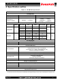
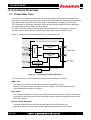
TIP-VBY1HS-DS
DATA SHEET
Preliminary
Preliminary
TIP-VBY1HS
Data Sheet
V-by-One® HS Standard IP
for Xilinx FPGA
Rev.1.00
Tokyo Electron Device Ltd.
Rev1.00
1
TIP-VBY1HS-DS
Revision History
The following table shows the revision history for this document.
Revision
Rev.1.0.0E
Rev1.00
Date
2010/04/12
Comments
First release
2
TIP-VBY1HS-DS
Table of Contents
1. Introduction ......................................................................................................................5
2. Features...........................................................................................................................5
3. References ......................................................................................................................5
4. Specification outline .........................................................................................................6
5. Functional Overview ........................................................................................................7
5.1. Transmitter Core................................................................................................................ 7
5.2. Receiver Core .................................................................................................................... 8
6. I/O Signals .......................................................................................................................9
6.1. Transmitter Core................................................................................................................ 9
6.2. Receiver Core .................................................................................................................. 10
7. Reference Clock ............................................................................................................11
7.1. Clock Construction.......................................................................................................... 11
7.2. Recommended Board Design .......................................................................................... 12
8. Parameterization............................................................................................................13
9. Verification .....................................................................................................................13
9.1. Simulation........................................................................................................................ 13
9.2. Hardware Validation ....................................................................................................... 13
10. Family Support.............................................................................................................14
11. Technical Support ........................................................................................................14
12. Ordering Information ....................................................................................................14
Rev1.00
3
TIP-VBY1HS-DS
Schedule of Figures
Figure 5.1
Figure 5.2
Figure 7.1
Figure 7.2
Figure 7.3
Transmitter Core Block Diagram .......................................................................7
Receiver Core Block Diagram ...........................................................................8
TIP-VBY1HS Clock Construction ....................................................................11
Transmitter FPGA Recommended Board Design............................................12
Receiver FPGA Recommended Board Design................................................12
Schedule of Tables
Table 4.1
Table 6.1
Table 6.2
Table 7.1
Table 7.2
Table 8.1
Rev1.00
TIP-VBY1HS Specification .................................................................................6
Transmitter Core I/O Signals ..............................................................................9
Receiver Core I/O Signals ................................................................................10
Virtex-6 GTX Reference Clock Characteristics.................................................11
Spartan-6 GTP Reference Clock Characteristics .............................................11
Parameterization Table ....................................................................................13
4
TIP-VBY1HS-DS
1. Introduction
V-by-One® HS standard has been developed by THine Electronics,Inc. to offer capabilities for Flat
Panel Display (FPD) markets that are requiring ever-higher frame rates and higher resolutions.
The TIP-VBY1HS Core provided by Tokyo Electron Device Ltd.(TED) is a high performance, flexible
solution for a high speed transmission of video signals designed to the V-by-One® HS standard for
the Xilinx FPGA.
State-of-the-art Virtex™-6 LXT / SXT and Spartan™-6 LXT are supported.
2. Features
Protocol compliant with V-by-One® HS standard provided by THine Electronics, Inc.
Independent Transmitter and Receiver module.
Supports 1, 2, 4, and 8 lanes operations.
Uses the GTP transceivers of Spartan-6 LXT families and the GTX transceivers
LXT /SXT families.
Supports up to 3.75Gbps data rate per lane (effective data rate 3Gbps) using Virtex-6 GTX
transceiver. (up to 3.125Gbps using Spartan-6 GTP transceivers)
Elastic buffers and Lane alignment
Data scrambling and Clock Data Recovery (CDR) to reduce EMI.
Variable settings of the driver swing, pre-emphasis.
Flexible implementation and package compatibility.
of Virtex-6
3. References
-
V-by-One®HS Standard Version 1.2 (Jan 15, 2009) by THine Electronics, Inc.
-
TIP-VBY1HS-TX(Transmitter)_UserManual
-
TIP-VBY1HS -RX(Receiver)_UserManual
-
TIP-VBY1HS_CVKReferenceDesign_UserManual
-
TIP-VBY1HS_Transceiver_PLL_Setting_EstimateSheet
-
Virtex-6 FPGA GTX Transceivers User Guide (UG366 v2.2 Feb 23, 2010)
-
Virtex-6 FPGA Data Sheet : DC and Switching Characteristics (DS152 v2.2 Feb 9,2010)
-
Spartan-6 FPGA GTP Transceivers User Guide (UG386 v2.1 Mar 30,2010)
-
Spartan-6 FPGA Data Sheet : DC and Switching Characteristics (DS162 v1.4 Mar 10,2010)
Rev1.00
5
TIP-VBY1HS-DS
4. Specification outline
Table 4.1 TIP-VBY1HS Specification
IP Facts
Core Specifics
Supported FPGA Family
Virtex-6 LXT/SXT
Spartan-6 LXT
-3, -2, -1
-3, -2
600Mbps ~ 3.75Gbps
614Mbps ~ 810Mbps
1.2288Gbps ~ 1.62Gbps
2.457Gbps ~ 3.125Gbps (1)
FPGA Speed Grade
Performance
(Serial Line Rate)
Core Resources ( in case of Spartan-6 )
Transmitter
Receiver
LANEs
GTP / GTX
FFs
LUTs
Block RAMs
1
1
~1,300
~900
8
2
2
~1,600
~1,000
10
4
4
~2,900
~2,300
20
8
8
~5,500
~4,700
40
1
1
~1,400
~1,000
6
2
2
~2,000
~1,500
10
4
4
~3,600
~2,600
20
8
8
~7,000
~5,200
40
PLLs
BUFGs
2 (2)
5 (2)
2 (2)
5 (2)
Core Highlights
Designed Verification
RTL Test Bench
Hardware Verification
Passed the connectivity test
Provided with Core
Documentation
Design File Formats
Instantiation Template
Constraints File
Verification
Data Sheet
Transmitter/Receiver Core User Manual
Transceiver_PLL_Setting_EstimateSheet (.xls)
Reference Design User Manual
NGC Netlist (Main Link module)
Verilog-HDL Wrapper
UCF(User Constraint File)
Timing Constraints
Transceiver Physical Constraints
Verilog Test Bench
Design Tool Requirements
Xilinx Implement Tools
ISE® 11.4 Logic Edition and above
Synthesis
Xilinx XST 11.4 and above
Simulation
Mentor Graphics® ModelSim® 6.5a and above
Support
Tokyo Electron Device Ltd.
(1) Spartan-6 LXT Speed grade -2 has a line speed limit up to 2.7Gbps.
(2) Number of the Clock resources (PLLs and BUFGs) will change according to the user logic, implementation and board circuit.
Rev1.00
6
TIP-VBY1HS-DS
5. Functional Overview
5.1. Transmitter Core
In the first, the Transmitter core allocates the video stream and control signals to the Main links
according to the number of the data lanes. Each Main Link transfers the allocated data through the
High-speed serial transceiver with framing, packet data mapping, scrambling, and encoding.
The Transmitter core also has a training function for the link start up with the receiver side while
checking the Hot plug and CDR Lock status signal.
In order to check the quality of the high-speed serial data lines, the Transmitter core has an
operation mode in which they act as the bit error tester (BET) called “Field BET mode”.
Figure 5.1 shows the function block diagram of the Transmitter core.
TIP_VBY1HS Transmitter (Wrapper)
Figure 5.1 Transmitter Core Block Diagram
The Transmitter core can be classified into the main function blocks as follows.
Main Link
The Main Link is a main function block provided as the netlist file (.ngc) .
Main Link consists of packer, scrambler, encoder, serializer, and transmitter link monitor.
Each data lane has own Main Link block.
Formatter
The Formatter interfaces to a user-driven stream of video data and control signals. According to
the number of the Main Links, this block allocates the video data and matches the timing to the
Main Link interface.
Clock / Reset Generator
This block makes all clocks and reset signals required in the Transmitter core.
Appropriate frequency clocks adjust the rate difference between the function blocks.
Rev1.00
7
TIP-VBY1HS-DS
5.2. Receiver Core
The Receiver core has a symmetrical function with the Transmitter core.
Each Main Links receives the data from the transmitter side through the High-speed serial
transceiver and regenerates the allocated data with decoding, de-scrambling, packet data
un-mapping, and de-framing. In the end, these framing data from the Main Links combined to
regenerate the original stream of video data and control signals.
The Receiver core also has a training function for the link start up with the transmitter side while
generating the Hot plug and CDR Lock status signal.
In order to check the quality of the high-speed serial data lines, the Receiver core has an operation
mode in which they act as the bit error tester (BET) called “Field BET mode”.
Figure 5.2 shows the function block diagram of the Receiver core.
Figure 5.2 Receiver Core Block Diagram
The Receiver core can be classified into the main function blocks as follows.
Main Link
The Main Link is a main function block provided as the netlist file (.ngc) .
Main Link consists of unpacker, de-scrambler, decoder, de-serializer, and receiver link monitor.
Each data lane has own Main Link block.
De-formatter
De-formatter matches the skew of the packet data from the Main Links and regenerates the
user-driven stream of video data and control signals from the allocated data in the Main Links.
Clock / Reset Generator
This block makes all clocks and reset signals required in the Receiver core from the recovery
clock from the transceiver in Main block.
Appropriate frequency clocks adjust the rate difference between the function blocks and
regenerate the pixel clock of the Transmitter side.
Rev1.00
8
TIP-VBY1HS-DS
6. I/O Signals
6.1. Transmitter Core
Table 6.1 Transmitter Core I/O Signals
Signal Name
Dedicated
External Pin
Direction
Polarity
Description
PDN
Input
‘L’
Power Down
REFCLK_P
Input
↑
MGTCLK for GTX/GTP Positive
✔
REFCLK_N
input
↑
MGTCLK for GTX/GTP Negative
✔
Main Link Interface
TX0_P [n:0]
Output
-
High-speed serial data lanes positive
✔
TX0_N [n:0]
Output
-
High-speed serial data lanes negative
✔
HTPDN
Input
‘L’
Hot plug detect
✔
LOCKN
Input
‘L’
Lock detect
✔
User Data Interface
PXCLK
Input
↑
Pixel Clock
VSYNC
Input
‘L’
Vertical sync pulse
HSYNC
Input
‘L’
Horizontal sync pulse
DE
Input
‘H’
Video data enable
DI [39:0]
(1)
Input
-
Video data
CTL [23:0]
(2)
Input
-
Control data
Mode Setting
DRV [3:0]
Input
-
Drive Strength Control
PRE [3:0]
Input
-
Pre-Emphasis Control
FIELD_BET
Input
‘H’
Field BET Mode Enable
Status Signal
RDY
output
‘H’
Link Status Ready
(1)
Video data width is dependent on the Byte Mode setting with byte boundary (24 / 32 / 40 bits) as following table.
(2)
Control data width is dependent on the Byte Mode setting with byte boundary (8 / 16 / 24 bits) as following table.
Byte Mode
DI [39:0]
3
23:0
4
5
Rev1.00
CTL [23:0]
7:0
31:0
39:0
15:0
23:0
9
TIP-VBY1HS-DS
6.2. Receiver Core
Table 6.2 Receiver Core I/O Signals
Signal Name
Dedicated
External Pin
Direction
Polarity
PDN
Input
‘L’
Power Down
REFCLK_P
Input
↑
MGTCLK for GTX/GTP Positive
✔
REFCLK_N
input
↑
MGTCLK for GTX/GTP Negative
✔
output
↑
Recovery clock out for External PLL
(optional)
✔
CLKOUT
Description
Main Link Interface
RX0_P [n:0]
Input
-
High-speed serial data lanes positive
✔
RX0_N [n:0]
Input
-
High-speed serial data lanes negative
✔
HTPDN
Output
‘L’
Hot Plug Detect
✔
LOCKN
Output
‘L’
Lock Detect
✔
User Data Interface
PXCLK
Output
↑
Pixel Clock
VSYNC
Output
‘L’
Vertical sync pulse
HSYNC
Output
‘L’
Horizontal sync pulse
DE
Output
‘H’
Video data enable
DO [39:0]
(1)
Output
-
Video Data
CTL [23:0]
(2)
Output
-
Control Data
Mode Setting
FIELD_BET
Input
‘H’
Field BET Mode Enable
Status Signal
FIELD_BET_CHK
Output
‘H’
Filed BET mode Check Error Status
(1)
Video data width is dependent on the Byte Mode setting with byte boundary (24 / 32 / 40 bits) as following table.
(2)
Control data width is dependent on the Byte Mode setting with byte boundary (8 / 16 / 24 bits) as following table.
Byte Mode
DO [39:0]
3
23:0
4
5
Rev1.00
CTL [23:0]
7:0
31:0
39:0
15:0
23:0
10
TIP-VBY1HS-DS
7. Reference Clock
7.1. Clock Construction
Besides the pixel clock, TIP-VBY1HS Transmitter and Receiver Core require the high quality
reference clock (REFCLK_P/N port) conforming to the GTP/GTX transceiver’s specification.
Especially, the REFCLK of the Receiver Core side is important because it’s frequency deviation is
limited to the transmission rate of the Data Lane.
Figure 7.1 TIP-VBY1HS Clock Construction
In addition, REFCLK is recommended to be supplied by the differential pair port and to be
satisfied the specification shown in Table 6.1 and Table 6.2. (For more information, refer to the
FPGA data sheets.)
Table 7.1 Virtex-6 GTX Reference Clock Characteristics
Symbol
FGCLK
TDCREF
Rxppmtol
Description
Reference clock frequency range
Reference clock duty cycle
Data/REFCLK PPM offset tolerance
Min
62.5
45
-200
Typ
50
-
Max
650
55
200
Units
MHz
%
ppm
Table 7.2 Spartan-6 GTP Reference Clock Characteristics
Symbol
Jitter
TDCREF
Rxppmtol
Description
Reference clock Jitter tolerance
Reference clock duty cycle
Data/REFCLK PPM offset tolerance
Min
60
45
-200
Typ
50
-
Max
160
55
200
Units
ps
%
ppm
Generally, frequency of the REFCLK is same to the pixel clock, it is also possible to use the
REFCLK of the frequency different from the pixel clock by setting the PLL of the GTP/GTX
Transceivers.
“TIP-VBY1HS Transceiver PLL Settings_EstimateSheet (Excel Sheet)” is useful to calculate the
frequency that can be set to the REFCLK.
Rev1.00
11
TIP-VBY1HS-DS
7.2. Recommended Board Design
Following Figures show the recommended REFCLK construction of the board.
Transmitter side
Figure 7.2 shows the construction of the Transmitter side.
It has the external PLL IC to clean-up the jitter of the pixel clock or synthesize the frequency that
Is required for the REFCLK input.
“M/D” block in the FPGA generates the appropriate frequency to the external PLL IC’s input, so
this block is optional.
PLL
Figure 7.2 Transmitter FPGA Recommended Board Design
Receiver side
Figure 7.3 shows the construction of the Receiver side.
In addition to the same purpose as the Transmitter side, the Receiver side has the external
VCXO PLL IC to generate the initial REFCLK of the frequency that is required for the Clock Data
Recovery (CDR) of the GTP/GTX Transceivers. After CDR is locked, this VCXO PLL should be
phase-locked to the recovery clock and generate the REFCLK of frequency that is completely
the same as the Transmitter side.
Figure 7.3 Receiver FPGA Recommended Board Design
Rev1.00
12
TIP-VBY1HS-DS
8. Parameterization
Table 8.1 Parameterization Table
Parameter Name
Values
P_FPGA_TYPE
0,1
P_LANE_NUM
1,2,4,8
P_BYTE_MD
3,4,5
Description
FPGA select
0:Virtex-6,
1:Spartan-6
Number of high-speed serial Data Lanes
Byte width of the video data
P_PLL_DIVSEL_xxx
(1)
PLL settings of the GTX/GTP transceivers
P_PXCLK_xxx
(2)
Settings of the PLL that generates the internal clock from the
pixel clock
P_GTPCLKOUT_xxx
(3)
Settings of the PLL that generates the internal clock from the
GTPCLKOUT port of the GTX/GTP transceivers
(1),(2),(3) Refer to the TIP-VBY1-TX/RX User Manual and GTX/GTP transceivers User Guide for the details of these parameters.
9. Verification
The TIP-VBY1HS Core has been verified with the RTL simulation and hardware validation of
connectivity test by THine Electronics, Inc.
9.1. Simulation
A highly-parameterizable command-based test bench was used to test the core.
All byte-modes and data lane numbers are tested by following construcition.
9.2. Hardware Validation
The TIP-VBY1HS Core has been validated using CVK kit of Tokyo Electron Device Ltd.(TED).
The hardware has been tested against the V-by-One® HS evaluation board from THine
electronics, Inc. for warranty of the connectibity.
Rev1.00
13
TIP-VBY1HS-DS
10. Family Support
The TIP_VBY1HS Core was designed to target the Virtex-6 and Spartan-6 FPGA families. This Core
can operate at full speed with the Virtex-6 all speed grades, and at limited speed with Spartan-6 each
speed grade part. Below is a list of supported device families.
- 600Mbps~3.75Gbps data rate per lane (same as the standard)
Virtex-6 LXT all speed grade
Virtex-6 SXT all speed grade
- 614Mbps~810Mbps, 1.2288Gbps~1.62Gbps, 2.457Gbps~3.125Gbps data rate per lane
Spartan-6 LXT -3 speed grade
- 614Mbps~810Mbps, 1.2288Gbps~1.62Gbps, 2.457Gbps~2.7Gbps data rate per lane
Spartan-6 LXT -2 speed grade
Fllowing equation shows how to determine the data rate of the lane (Gbps).
fDataRate = (
BITByteMode ×
fPixelClk ×
1.25(8B/10B) ) / NLane
Example
Byte-mode = 4byte, Pixel Clock frequency = 148.5MHz, Number of data lanes = 2
Data rate per lane = ( 32bit × 148.5MHz × 1.25 ) / 2 = 2.97Gbps
11. Technical Support
Tokyo Electron Device Ltd. (TED) provides technical support for this IP Core when used as
described in the product documentation. TED cannot guarantee timing, functionality, or support of
product if implemented in devices that are not defined in the documentation, if customized beyond
that allowed in the product documentation, of if changes are made to any section of the design
labeled DO NOT MODIFY.
TED also offers a reference design with their evaluation board and a contract-based development
service for customized design or additional function design (ex. more than 16 data lanes for Virtex-6).
12. Ordering Information
Rev1.00
14
TIP-VBY1HS-DS
memo
Rev1.00
15
TIP-VBY1HS-DS
Tokyo Electron Device Limited
Inrevium Division
Yokohama East Square
1-4, Kinko-cho, Kanagawa-ku,
Yokohama City, Kanagawa 221-0056, Japan
TEL:+81-45-443-4031
FAX:+81-45-443-4059
URL: http://www.inrevium.jp/eng
Email: [email protected]
Your Local Contact:
- The Information described in this document will be changed from time to time without prior notice. If you plan
to buy and use this device product described herein, please contact the sales person or address specified herein.
- Tokyo Electron Device Limited shall not be liable for any claim by third party alleging an infringement of
patent right or any other intellectual property right, where alleged liability of Users arises by reason of using the
information and drawing described in this document.
- Tokyo Electron Device Limited shall not be liable for any claim by third party alleging an infringement of the
patent right, utility model right, circuit layout use right, copyright, or any other intellectual property right,
where alleged liability of Users arises by reason of using this device product in combination with other products,
or of any derivative products integrating this device product.
-
This device product is not designed, manufactured, or intended for use (1) in hazardous environment requiring
extremely high safety including without limitation, in operation of nuclear reaction control in nuclear facility,
aircraft flight control, air traffic control, mass transport control, medical life support system, missile launch
control in weapon system in which the failure of this device product could have a serious effect to the public and
lead directly to death, personal injury, severe physical damage or other loss, or (2) in any other environment
requiring extremely high reliability including without limitation in operation of submarine transmissions or
space satellite.
2010 Tokyo Electron Device Limited
Rev1.00
printed in Japan
Apr. 2010
16