1
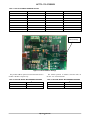
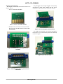
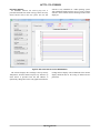
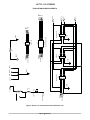
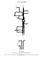
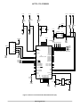
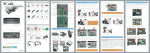
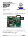
NCT75-175-275GEVB
NCT75-175-275
Evaluation Board
User's Manual
About This Manual
www.onsemi.com
This manual will enable the user to use NCT75−175−275
Evaluation Board to evaluate functional performance of the
following ON Semiconductor devices.
• NCT75
• NCT175
• NCT275
EVAL BOARD USER’S MANUAL
of dedicated daughter cards. The device’s features are tested
by using a digital interface cable along with the supported
software. The test results should be taken to judge the device
functional performance according the specification in the
technical datasheet.
These devices can be tested either by soldering them on
the board or by using a dedicated daughter card for that
device. Footprints of different packages are provided and
marked for different package options of these devices.
Similarly a DIP socket is also provided to facilitate the use
Power-on LED
ALERT LED
Footprints
Socket for
Daughter Cards
Figure 1. NCT75−175−275 Evaluation Board Showing the Footprints and the 8-pin
DIP Socket for the Daughter Cards
Power & ALERT LEDs
Address Selection
NCT75−175−275 board is powered up by a 3.3 V
internally generated power supply. The board is designed in
such a manner that devices’s fucntionality can be tested
without the need of an externally supplied power (other than
USB 5 V). Green LED D7 shows that a 3.3 V is available.
In order to display any out of limit condition a red colored
ALERT LED D3 is provided on the board.
NCT75 & NCT175 are available with 9 possible
addresses as they have three address pins A0, A1 and A2
respectively. NCT275 is available in two possible addresses
with one address pin A1. Links LK7, LK1 & LK2
corresponds address selection of A0, A1 and A2
respectively.
The possible address options for NCT75/175 are shown in
Table 1.
© Semiconductor Components Industries, LLC, 2014
October, 2014 − Rev. 0
1
Publication Order Number:
EVBUM2271/D
NCT75−175−275GEVB
Table 1. NCT75/175 SMBUS ADDRESS OPTION
A2
A1
A0
Address
0
0
0
0x48
0
0
1
0x49
0
1
0
0x4A
0
1
1
0x4B
1
0
0
0x4C
1
0
1
0x4D
1
1
0
0x4E
1
1
1
0x4F
Links for
Address Settings
Figure 2. Links for Address Settings
The possible address options for NCT275A/B are shown
in Table 2 & Table 3 respectively.
The default position of address selection links on
NCT75−175−275 board is 000.
Table 2. NCT275A SERIAL BUS ADDRESS OPTIONS
Table 3. NCT275B SERIAL BUS ADDRESS OPTIONS
Ball B1
I2C
Address
Ball B1
I2C Address
0
0x49
0
0x48
1
0x4B
1
0x4A
http://onsemi.com
2
NCT75−175−275GEVB
Daughter Card for NCT275
The photograph of the complete daughter card assembly
for NCT275 is show below. Please note the correct
orientation of CSP board in to the SULLENs connector.
The daughter card assembly for NCT275 consists of two
PCBs as follows:
1. NCT75−CSP−EDGE−BOARD
Figure 3. NCT75−CSP−EDGE−BOARD
2. BOARD with a SULLENs socket for the EDGE
Board and the 8-pin DIP connector for the mother
board interface.
Figure 6. NCT−275 Daughter Card Assembly
The daughter card assembly is now ready to be plugged in
to the NCT75−175−275 board. The picture of the said setup
is shown in Figure 7.
Figure 4. SULLENS Board Showing the DIP−8
Connector
Figure 7. NCT−275 Test Setup
Figure 5. SULLENS Board Showing the Socket for
CSP Board
http://onsemi.com
3
NCT75−175−275GEVB
Evaluation Software
software is only installable on a 64bit operating system.
After installation double click the NCT75.exe file to run the
software. As the software runs the following window will be
displayed:
An installable software file NCT75_x64_v1.0.0 is
provided. Install this file which will copy all the necessary
drivers and hex files in the user system. For now this
Figure 8. GUI of the NCT75−175−275 EVB Software
readings in these displays. The left hand side of the window
displays different tabs for the setting of different device
parameters.
The software displays three readings at the top namely
Temperature, TOS and THYST respectively. Numeric up
down menus is provided with OS and THYST to
dynamically change these values. The graphs will follow the
http://onsemi.com
4
SDA
SCL
OS/ALERT
OS/ALERT
ALERT
R1
0
ALERT-PULLUP
D3
Red
R3
1k
+3.3V
http://onsemi.com
5
AGND
Figure 9. NCT75−175−275 Evaluation Board Schematic (1/4)
NCT75
8
7
6
5
1
2
3
4
8
7
6
5
NCT75
U12
U11
1
2
3
4
SOIC8
AGND
GND
SDA
SCL
OS/ALERT
SDA
SCL
OS/ALERT
DGND
Micro8 3 X 3
AGND
GND_4 GND_3GND_2 GND_1
1
2
3
4
U1
6
5
4
8
7
6
5
8
7
6
5
NCT75
U13
AGND
1
2
3
4
DFN8 2 x 2
SKT NCT75/175/275
DIP8
U10
NCT275
6 Ball CSP
1
2
3
AGND
VDD
A1
GND
A1
A2
A0
VDD
VDD
A0
A1
A2
NCT75−175−275GEVB
EVALUATION BOARD SCHEMATIC
R10
0
6
J6-3
J6-2
J6-1
SCL
SDA
I2C OVERDRIVE
DGND
PA2
PA0
PA1
R24
3.3k
+3.3V
R26
3.3k
R28
3.3K
http://onsemi.com
DGND
U6
8
7
6
5
SN74LVC3G07
1
2
3
4
+3.3V
R11
3.3k
SCL-PULLUP
+3.3V
0
R27
SCL
R12
3.3k
R25
0
SDA
SCL
SDA
SDA-PULLUP
NCT75−175−275GEVB
Figure 10. NCT75−175−275 Evaluation Board Schematic (2/4)
NCT75−175−275GEVB
+3.3V
R15
100k
+3.3V
+3.3V
R6
100k
+3.3V
R16
0R
0.1uF
C13
+
+
C15
0.1uF
C11
10uF
C8
2.2uF
+3.3V
0.1uF
+3.3V
5VUSB
IO
GND
3
4
42
RESET
44
*WAKEUP
5
54
CLKOUT
9
D8
D+
DGND
33
34
35
36
37
38
39
40
PA0
PA1
PA2
U5
CY7C68013-CSP
PA0/INT0
PA1/INT1
PA2/*SLOE
PA3/*WU2
PA4/FIFOADR0
PA5/FIFOADR1
PA6/*PKTEND
PA7/*FLD/SLCS
PB0/FD0
PB1/FD1
PB2/FD2
PB3/FD3
PB4/FD4
PB5/FD5
PB6/FD6
PB7/FD7
PD0/FD8
PD1/FD9
PD2/FD10
PD3/FD11
PD4/FD12
PD5/FD13
PD6/FD14
PD7/FD15
CTL0/*FLAGA
CTL1/*FLAGB
CTL2/*FLAGC
SDA
SCL
1
RDY0/*SLRD
2
RDY1/*SLWR
13
IFCLK
14
RSVD
AGND
R14
10k
XTALOUT
6
DGND
7
11
17
27
32
43
55
3
2
DGND
PB0 PB1 PB2 PB3
XTALIN
18
19
20
21
22
23
24
25
45
46
47
48
49
50
51
52
PB0
PB1
PB2
PB3
LAYOUT PORTB PINS TOGETHER
29
30
31
16
15
4
5
GND
GND
GND
GND
GND
GND
GND
D+
I2C Address = 1010 001
Y1
10
12
26
28
41
53
56
D-
1
VCC
VCC
VCC
VCC
VCC
VCC
VCC
SHIELD
U3
8
VCC
7
WP
6
SCL
5
SDA
DGND
AVCC
VBUS
R18
3.3k
C6
24LC64
1
A0
2
A1
3
A2
4
VSS
J4
USB-MINI-B
+3.3V +3.3V
C3
22pF
DGND
1
3
2
4
C4
22pF
DGND
XTAL-ABM3B
DGND
DGND
Figure 11. NCT75−175−275 Evaluation Board Schematic (3/4)
http://onsemi.com
7
R19
D22
+
C5
0.1uF
10uF
AGND
1
2
3
U2
6
5
4
CAT6221
CAT6221-SGTD-GT3
C14
5V
A0
AGND
1uF
C9
3.3V
R33
AGND
LK7
+3.3V
Green
D7
1K
+3.3V
A1
C1
10uF
5VUSB
B
A
+
R9
0
AGND
AGND
LK1
+3.3V
A2
LAYOUT CAPS NEAR TO THREE FOOT PRINTS
0.1u
C2
B
8
AGND
LK2
+3.3V
VDD
B
http://onsemi.com
A
Figure 12. NCT75−175−275 Evaluation Board Schematic (4/4)
A
+3.3V
VDD
NCT75−175−275GEVB
NCT75−175−275GEVB
Table 4. NCT75−175−275 EVB BILL OF MATERIAL
Item
Qty
Reference
Description
PCB Decal
Stock Code
1
Y1
Crystal SMD 24 MHz
Abracorn Cooperation
CRY−ABM3B
535−9700−1−ND (Digi-key)
2
1
U6
SN74LVC3G07DCTR Triple Buffer
DCT−R−PDSO−8
FEC 1601176RL
3
1
U5
USB Microcontroller
(CY7C68013A−56LTXC)
LFCSP−56
Digi-key 428−2933−ND
4
1
U3
24LC64 64K I2C Serial EEPROM
SO8NB
FEC 9758070
5
1
U2
CAT6221−SFTD−GT3 300 mA Dual
LDO Regulator, 3.3 V/1.5 V
TSOT−23
ON Semiconductor SUPPLIED
6
1
U13
NCT75
DFN8−2X2−0.5P
DONOT POPULATE
7
1
U12
NCT75
SO8NB
DONOT POPULATE
8
1
U11
NCT75
USOIC−8
DONOT POPULATE
9
1
U10
IC SOCKET, DIP, 8POS, 2.54MM
DIP8
FEC 1925018
10
1
U1
NCT275
WLCSP−6−0.4MM
DONOT POPULATE
CRYSTALS
1
ICs
RESISTORS
11
2
R6, R15
Resistor 100 kW, 0603, 0.125, 1%,
Multicomp
603
FEC 1576310
12
1
R33
Resistor 1 kW, 0805, 100 mW, 1%,
Multicomp
805
FEC 9332383
13
1
R3
RESISTOR, THICK FILM, 1 kW,
0.125 W, 1%
603
FEC 1576283
14
1
R14
Resistor 10 kW, 0603, 0.125W, 1%,
Multicomp
603
FEC 1576297
15
7
R11, R12
R18, R19,
R24, R26,
R28
Resistor 3.3 kW, 0603, 63 mW, 5%,
Multicomp
603
FEC 9332022
16
6
R1, R9, R10,
R16, R25,
R27
Resistor 0R, 0603, 0.1 W, 1%,
CRCW06030000Z0EA Vishay
603
FEC 1469739
3
LK1, LK2,
LK7
HEADER, 1ROW, 3WAY & JUMPER
2 PIN PCB
LINK−3P
FEC 1022245 & 1654800
LINKS
17
CONNECTORS
18
1
J6
TERMINAL BLOCK. PCB,3.81MM,
3WAY Phoenix Contact
CON−3W−3.81MM
FEC 3704580
19
1
J4
USB Mini−B Receptacle Molex
USB−MINI−B
FEC 9786490
20
1
D7
HSMG−C170 − LED, GREEN,
15MCD, 572NM
805
FEC 5790852
21
1
D3
MULTICOMP − 703−0107 − LED,
0805, RED, 15MCD, 643NM,
805
FEC 2112119
22
1
D22
DIODE, SCHOTTKY, SOT−23
SOT23
FEC 9526765
DIODES
http://onsemi.com
9
NCT75−175−275GEVB
Table 4. NCT75−175−275 EVB BILL OF MATERIAL (continued)
Item
Qty
Reference
Description
PCB Decal
Stock Code
CAPACITORS
23
1
C9
CAP MLCC, 1 mF, 25 V, X5R, 10%,
0603, REEL
603
FEC−2280849
24
1
C8
CAP 2.2 mF, 10 V SMD Tantalum
Capacitor
RTAJ_A
FEC 498−646
25
5
C2, C5, C6
C13, C15
CAPACITOR, 0603, 0.1 mF, 25 V
Multicomp
603
FEC 9406204
26
2
C3, C4
CAP 22 pF, 50 V, SMD Ceramic
Capacitor Yageo
603
FEC 722005
27
3
C1, C11,
C14
CAP 10 mF, 10 V SMD Tantalum
Capacitor
CAP\TAJ_A
FEC 197−130
TEST POINTS
28
9
TERMINAL, PCB, YELLOW, PK 100 VERO
TESTPOINT
FEC 8731187
29
2
TERMINAL, PCB, RED, PK100 VERO
TEST POINT
FEC 8731144
30
5
HARWIN − M20−9990246 − HEADER, 1ROW, 2WAY
TEST POINT
FEC 1022247
ON Semiconductor and the
are registered trademarks of Semiconductor Components Industries, LLC (SCILLC) or its subsidiaries in the United States and/or other countries.
SCILLC owns the rights to a number of patents, trademarks, copyrights, trade secrets, and other intellectual property. A listing of SCILLC’s product/patent coverage may be accessed
at www.onsemi.com/site/pdf/Patent−Marking.pdf. SCILLC reserves the right to make changes without further notice to any products herein. SCILLC makes no warranty, representation
or guarantee regarding the suitability of its products for any particular purpose, nor does SCILLC assume any liability arising out of the application or use of any product or circuit, and
specifically disclaims any and all liability, including without limitation special, consequential or incidental damages. “Typical” parameters which may be provided in SCILLC data sheets
and/or specifications can and do vary in different applications and actual performance may vary over time. All operating parameters, including “Typicals” must be validated for each
customer application by customer’s technical experts. SCILLC does not convey any license under its patent rights nor the rights of others. SCILLC products are not designed, intended,
or authorized for use as components in systems intended for surgical implant into the body, or other applications intended to support or sustain life, or for any other application in which
the failure of the SCILLC product could create a situation where personal injury or death may occur. Should Buyer purchase or use SCILLC products for any such unintended or
unauthorized application, Buyer shall indemnify and hold SCILLC and its officers, employees, subsidiaries, affiliates, and distributors harmless against all claims, costs, damages, and
expenses, and reasonable attorney fees arising out of, directly or indirectly, any claim of personal injury or death associated with such unintended or unauthorized use, even if such claim
alleges that SCILLC was negligent regarding the design or manufacture of the part. SCILLC is an Equal Opportunity/Affirmative Action Employer. This literature is subject to all applicable
copyright laws and is not for resale in any manner.
PUBLICATION ORDERING INFORMATION
LITERATURE FULFILLMENT:
Literature Distribution Center for ON Semiconductor
P.O. Box 5163, Denver, Colorado 80217 USA
Phone: 303−675−2175 or 800−344−3860 Toll Free USA/Canada
Fax: 303−675−2176 or 800−344−3867 Toll Free USA/Canada
Email: [email protected]
N. American Technical Support: 800−282−9855 Toll Free
USA/Canada
Europe, Middle East and Africa Technical Support:
Phone: 421 33 790 2910
Japan Customer Focus Center
Phone: 81−3−5817−1050
http://onsemi.com
10
ON Semiconductor Website: www.onsemi.com
Order Literature: http://www.onsemi.com/orderlit
For additional information, please contact your local
Sales Representative
EVBUM2271/D