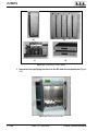
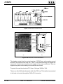
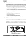
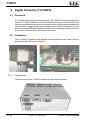
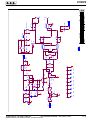
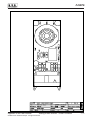
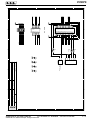
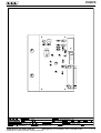
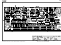
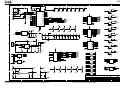
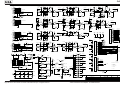
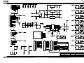
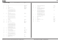
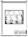
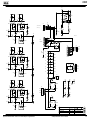
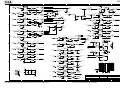
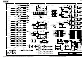
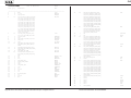
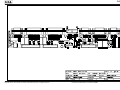
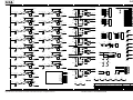
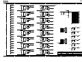
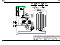
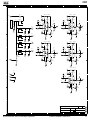
1
PJ5KPS
User & Technical
Manual
Manifactured by
Italy
PJ5KPS - Use and maintenance manual
Versione 1.5
© Copyright 2003-2006
R.V.R. Elettronica SpA
Via del Fonditore 2/2c - 40138 - Bologna (Italia)
Telefono:
+39 051 6010506
Fax:
+39 051 6011104
Email:
[email protected]
Web:
www.rvr.it
All rights reserved
Printed and bound in Italy. No part of this manual may be reproduced,
memorized or transmitted in any form or by any means, eletronic or
mechanic, including photocopying, recording or by any information
storage and retrieval system, whithout the permission of the copyright
owner.
D o cu m en t H isto ry
D ate
30/01/02
V ersion
1.0
24/10/02
1.1
18/11/02
1.2
19/12/03
31/10/05
08/02/06
1.3
1.4
1.5
R eason
F irst V ersion
G eneral R evision. N ew form at (P ageM aker). Insert
of chapter 8. T echnical appen dix integrated.
S tand-by functions update. P ow er-on procedu re
corrections. N ew section chap.8 I/O interface board.
N ew schem atic version of W iring diagram and
P S S W 5040
Insert of chapter 9. T echnical A ppendix upgradated.
S LP W R M T R P J5 B oard U pgrade
S L042M T 1001 and S L042R F 1001 board upgrading
E ditor
D . C anazza
D . C anazza
D . C anazza
J. B erti
J. B erti
J. B erti
Notification of intended purpose and limitations of product use
This product is a FM transmitter intended for FM audio broadcasting. It utilises
operating frequencies not harmonised in the intended countries of use.
The user must obtain a license before using the product in intended country of
use. Ensure respective country licensing requirements are complied with.
Limitations of use can apply in respect of operating freuency, transmitter power
and/or channel spacing.
Declaration of Conformity
Hereby, R.V.R. Elettronica SpA, declares that this FM transmitter is in
compliance with the essential requirements and other relevant provisions of
Directive 1999/5/EC.
This page intentionally left blank
PJ5KPS
Table of Contents
1.
2.
3.
3.1
3.2
4.
4.1
4.2
4.3
4.4
5.
5.1
5.2
5.3
5.4
5.5
6.
7.
7.1
7.2
7.3
7.4
7.5
7.6
8.
8.1
8.2
8.3
8.4
8.5
8.6
8.7
8.8
9.
9.1
9.2
9.3
Introduction
Warranty
First Aid
Treatment of electrical shocks
Treatment of electrical Burns
General Description
Composition
Technical specifications
Options
Operating principles
Installation and use
Assembly
Amplifier check
First start
Management of the exciters
Protection and alarms
Troubleshooting
Technical description
Software - Reference guide
Parallel Interface
Power supply section
RF Modules amplifier
Alarms
Combiner and divider
Technical Notes
Microcontrol board Trimmers
Phase Adhutment of RF modules
Splitter board trimmers
Parallel Interface
RF module I/O Interface
Services supply
Emergency CCU Board
PJ5KPS Ventilation
Digital Telemetry (TLC5KPS)
Foreword
Installation
Technical details
User & Technical Manual
Rev. 1.5- 08/02/06
1
3
5
5
6
7
7
7
8
8
11
11
15
18
21
24
25
26
26
38
42
49
50
52
53
53
54
54
55
56
57
58
62
64
64
64
76
i
PJ5KPS
This page was intentionally left blank
ii
Rev. 1.5- 08/02/06
User & Technical Manual
PJ5KPS
1. Introduction
This manual describes the PJ5KPS, a solid-state RF amplifier designed for
frequency modulation sound broadcasting, manufactured by R.V.R. Elettronica.
The PJ5KPS amplifier constitutes the end power section for FM transmitters fitted
with different possible configurations. A control system for the exciters is built into
the machine so that in order to have a system with redundant exciters, all that
needs to be done is to include two exciters in the transmitter such as, for example,
the PTX30LCD exciters made by R.V.R. Elettronica.
The manual is structured as follows:
•
Chapter 1: Presentation of the manual
•
Chapter 2: Warranty conditions
•
Chapter 3: Safety recommendations
•
Chapter 4: Description of the machine and its operating principles
•
Chapter 5: Guide for installation and use
•
Chapter 6: Most frequent troubleshooting cases on starting up the machine
•
Chapter 7: In-depth description of the operation of the modules of the apparatus.
This chapter also contains the description of the pin configuration of the
connectors and explains how to use the control unit menus, item by item.
•
Chapter 8: technical notes.
•
Appendix: It contains all the design details (wiring diagrams, assembly plans,
etc.) of the PJ5KPS.
This manual is written as a general guide for those having previous knowledge
and experience with this kind of equipment, well conscious of the risks connected
with the operation of electrical equipment.
It is not intended to contain a complete statement of all safety rules which should
be observed by personnel in using this or other electronic equipment.
The installation, use and maintenance of this piece of equipment involve risks
both for the personnel performing them and for the device itself, that shall be used
only by trained personnel.
R.V.R. Elettronica SpA doesn’t assume responsibility for injury or damage resulting
from improper procedures or practices by untrained/unqualified personnel in the
handling of this unit.
Please observe all local codes and fire protection standards in the operations of
this unit.
WARNING: always disconnect power before opening covers or removing any
part of this unit.
Use appropriate grounding procedures to short out capacitors and high voltage
User & Technical Manual
Rev. 1.5 - 08/02/06
1 / 80
PJ5KPS
points before servicing.
WARNING: this device can irradiate radio frequency waves, and if it’s not installed
following the instructions contained in the manual and local regulations it could
generate interferences in radio communications.
This is a "CLASS A" equipment. In a residential place this equipment can cause
hash. In this case can be requested to user to take the necessary measures.
R.V.R. Elettronica SpA reserves the right to modify the design and/or the technical
specifications of the product and this manual without notice.
2 / 80
Rev. 1.5 - 08/02/06
User & Technical Manual
PJ5KPS
2. Warranty
Any product of R.V.R. Elettronica is covered by a 24 (twentyfour) month warranty.
For components like tubes for power amplifiers, the original manufacturer’s warranty
applies.
R.V.R. Elettronica SpA extends to the original end-user purchaser all
manufacturers warranties which are transferrable and all claims are to be made
directly to R.V.R. per indicated procedures.
Warranty shall not include:
1 danni verificatisi durante la spedizione della macchina alla R.V.R. per eventuali
riparazioni;
2 Any unauthorized repair/modification;
3 Incidental/consequential damages as a result of any defect
4 Nominal non-incidental defects
5 Re-shipment costs or insurance of the unit or replacement units/parts
Any damage to the goods must be reported to the carrier in writing on the shipment
receipt.
Any discrepancy or damage discovered subsequent to delivery, shall be reported
to R.V.R. Elettronica within 5 (five) days from delivery date.
To claim your rights under this warranty, you shold follow this procedure:
1 Contact the dealer or distributor where you purchased the unit. Describe the
problem and, so that a possible easy solution can be detected.
Dealers and Distributors are supplied with all the information about problems
that may occur and usually they can repair the unit quicker than what the
manufacturer could do. Very often installing errors are discovered by dealers.
2 If your dealer cannot help you, contact R.V.R. Elettronica and explain the
problem. If it is decided to return the unit to the factory, R.V.R. Elettronica
will mail you a regular authorization with all the necessary instructions to send
back the goods.
3 When you receive the authorization, you can return the unit. Pack it carefully
for the shipment, preferably using the original packing and seal the package
perfectly. The customer always assumes the risks of loss (i.e., R.V.R. is never
responsible for damage or loss), until the package reaches R.V.R. premises.
For this reason, we suggest you to insure the goods for the whole value.
Shipment must be effected C.I.F. (PREPAID) to the address specified by R.V.R.’s
service manager on the authorization
DO NOT RETURN UNITS WITHOUT OUR AUTHORIZATION AS THEY WILL
BE REFUSED
User & Technical Manual
Rev. 1.5 - 08/02/06
3 / 80
PJ5KPS
4 Be sure to enclose a written technical report where mention all the problems found
and a copy of your original invoice establishing the starting date of the warranty.
Replacement and warranty parts may be ordered from the following address. Be
sure to include the equipment model and serial number as well as part description
and part number.
R.V.R. Elettronica SpA
Via del Fonditore, 2/2c
40138 BOLOGNA
ITALY
Tel. +39 051 6010506
4 / 80
Rev. 1.5 - 08/02/06
User & Technical Manual
PJ5KPS
3. First Aid
The personnel employed in the installation, use and maintenance of the device,
shall be familiar with theory and practice of first aid..
3.1
3.1.1
Treatment of electrical shocks
If the victim is not responsive
Follow the A-B-C's of basic life support
•
Place victim flat on his backon a hard surface.
•
Open airway: lift up neck, push forehead back (Fig. 3-1).
•
clear out mouth if necessary and observe for breathing
•
if not breathing, begin artificial breathing (Figure 3-2): tilt head, pinch nostrils,
make airtight seal, four quick full breaths. Remember mouth to mouth
resuscitation must be commenced as soon as possible
Figure 3-1
•
Figure 3-2
Check carotid pulse (Fig 3-3); if pulse is absent, begin artificial circulation
(Fig. 3-4) depressing sternum (Fig. 3-5)
Figure 3-3
Figure 3-4
Figure 3-5
•
In case of only one rescuer, 15 compressions alternated to two breaths.
•
If there are two rescuers, the rythm shall be of one brath each 5 compressions.
•
Do not interrupt the rythm of compressions when the second person is giving
breath.
•
Call for medical assistance as soon as possible.
User & Technical Manual
Rev. 1.5 - 08/02/06
5 / 80
PJ5KPS
3.1.2
3.2
3.2.1
If victim is responsive
•
Keep them warm
•
Keep them as quiet as possible
•
Loosen their clothing (a reclining position is recommended)
•
Call for medical help as soon as possible
Treatment of electrical Burns
Extensive burned and broken skin
•
Cover area with clean sheet or cloth
•
Do not break blisters, remove tissue, remove adhered particles of clothing, or
apply any salve or ointment.
•
Treat victim for shock as required.
•
Arrange transportation to a hospital as quickly as possible.
•
If arms or legs are affected keep them elevated
If medical help will not be available within an hour and the victim is conscious and
not vomiting, give him a weak solution of salt and soda: 1 level teaspoonful of salt
and 1/2 level teaspoonful of baking soda to each quart of water (neither hot or
cold). Allow victim to sip slowly about 4 ounces (half a glass) over a period of 15
minutes. Discontinue fluid if vomiting occurs
DO NOT give alcohol
3.2.2
6 / 80
Less severe burns
•
Apply cool (not ice cold) compresses using the cleansed available cloth article.
•
Do not break blisters, remove tissue, remove adhered particles of clothing, or
apply salve or ointment.
•
Apply clean dry dressing if necessary.
•
Treat victim for shock as required.
•
Arrange transportation to a hospital as quickly as possible
•
If arms or legs are affected keep them elevated.
Rev. 1.5 - 08/02/06
User & Technical Manual
PJ5KPS
4. General Description
The PJ5KPS is a RF amplifier for frequency modulation sound broadcasting. It is a
fully solid-state apparatus of modern design that uses MOSFET as active components
in the FM amplifying modules. This chapter briefly describes the machine's main
features.
4.1
Composition
The PJ5KPS amplifier is made up of modules inserted in a 19" rack. The main
modules are as follows:
•
1 Control unit
•
5 1.2 kW RF amplifier modules
•
1 Control unit
•
1 or 2 Power supply unit carriages
•
1 Splitter/Input RF
The amplifier is supplied complete with all its parts, not really "modules", essential
for its operation such as the fans for dissipating the heat generated by the machine
inside the room and all the accessories for the electrical and RF wiring. As a rule, the
amplifier is supplied as a complete transmitter therefore the two FM exciters that it
manages will be provided and connected (a service exciter and a spare exciter).
4.2
Technical specifications
Frequency range
Nominal RF power
Power supply voltage
Exciting power
Consumption
Power factor
87.5 to 108.0 MHz
5000 W
380 Three-phase, 3F+N
Max. 30 W
< 9.5 kW
> 0.95
Additional important features of the PJ5KPS are as follows:
•
The 1.2 kW amplifying modules are implemented by means of plug-in technology:
the individual modules may be removed for performing maintenance operations,
for instance, without having to turn off the transmitter. The transmitter keeps working
at reduced power even if the module has been removed. This operation may be
carried out without any risk of damaging the module itself, or the amplifier as a
whole, thanks to the control system and to the RF connectors, the power supply
and the purposely designed data-exchange. For further information refer to the
maintenance section.
•
Each module is controlled by a microprocessor-based card that checks and
adjusts its operating mode. The resulting data are transmitted to the control unit.
•
The control unit manages the changeover of the two exciters both in automatic
and manual mode.
User & Technical Manual
Rev. 1.5 - 08/02/06
7 / 80
PJ5KPS
4.3
•
The amplifier may be equipped with a dual power supply/rectifier module. Both
modules operate in this case the configuration is in “hot stand-by” since both
supply, when operating under normal conditions, half of the current required by
the machine to work. When one module is absent or faulty, the module that is
present supplies all the required current by itself. The sufficient dimensioning of
each power supply unit guarantees that the machine will work efficiently at its
nominal power level.
•
The amplifier can work as usual even if the control unit is not present. In fact, the
control unit may be substituted temporarily with an electromechanical interface
by means of which the user may give the ON and OFF commands to the machine.
However, in this case all the numeric type information will be missing and the
power level remains the last one enabled before removing the control unit.
Options
The PJ5KPS envisages the following options:
4.4
•
Single or dual power supply carriage
•
Single or dual exciter
•
N+1 configuration
•
Different kinds of exciters
•
Automatic restore after safety tripping or manual restore
Operating principles
This description is based on the block diagram shown in Figure 4-1.
The PJ5KPS amplifier essentially comprises three blocks:
•
The power supply section
•
The Splitter-Coupler section
•
The RF amplifier section
The power supply section of the PJ5KPS amplifier is made up of one or two threephase transformers, each one associated with a rectifier circuit for generating the
non-stabilized voltage of 80V that supplies the RF modules. The transformers and
the rectifier circuits are mounted on removable carriages together with power
inductors that help achieve a power factor of about 94%.
The power supply unit carriage is dimensioned for supplying all the power required
for the PJ5KPS to operate at full power. Therefore the configuration of the machine
with two power supply unit carriages is a hot stand-by redundant one.
The power supply section is controlled by a microprocessor-based card installed in
the rack.
The Splitter-Coupler section performs all the treatment of the RF signal except for the
power amplification.
8 / 80
Rev. 1.5 - 08/02/06
User & Technical Manual
RS485
μC
Tansformer
/Rectifier
Tansformer
/Rectifier
AC in
380 V
3F+N
Control Unit
-6 dB
Exc. 2
RF in
Exc. 1
RF in
-6 dB
RS485
Splitter
80 Vdc
Power
setting
μC
Power
supply
-
RS485
1.2 kW RF Module (5x)
μC
RS485
Coupler
RF Out
PJ5KPS
Figure 4-1 Block diagram of the PJ5KPS
The RF signals generated by two exciters (in the redundant configuration) are first
attenuated by 6 dB to improve the uncoupling among the stages and then connected
to a coaxial relay commanded by the control unit. One of the two signals is closed on
a dummy load built into the machine whereas the other signal is connected to the
input splitter. The power of both signals is measured by specific directional couplers.
The RF signal of the selected exciter is divided into five branches, each of which is
passed to the input of an amplifying module.
User & Technical Manual
Rev. 1.5 - 08/02/06
9 / 80
PJ5KPS
The five RF amplifiers branches are recombined by the coupler at the output of the
amplifying modules. The overall amplified RF signal is filtered by a low-pass filter for
eliminating the harmonics and is therefore available at the output connector.
The Splitter-Coupler section is controlled by a microprocessor-based card, which
makes the values detected at the various measuring points available for the user
and for the diagnostics functions.
The machine contains five RF amplifier modules each of which is capable of supplying
a maximum of 1.2 kW RF. Each module includes a switching mode power supply unit
that regulates and stabilizes the power supply voltage supplied by the power supply
section.
Each amplifying module contains a first stage with gain that varies according to the
MOSFET BLF175. The RF signal amplified by the driver is then separated into four
branches, amplified by four modules based on BLF 278, recombined and filtered by
a low-pass filter.
Each RF amplifying module is controlled by a microprocessor-based card, connected
to the other microprocessor-based cards of the machine by means of a RS485 type
bus.
Each module runs the Automatic Power Control function for regulating the supplied
power: the gain of the amplifying stages and the voltage supplied by the switching
power supply unit are regulated so that the power that is output from the module
corresponds, if possible, to the set level.
The overall power that the PJ5KPS must supply is controlled by the microprocessorbased card of the splitter-combiner section according to the settings made on the
control unit for the NOMINAL POWER and LOWER POWER parameters.
10 / 80
Rev. 1.5 - 08/02/06
User & Technical Manual
PJ5KPS
5. Installation and use
This chapter contains the basic instructions for installing and using the PJ5KPS
amplifier. If necessary, more in-depth information about the operating principles may
be traced in the next chapters.
5.1
Assembly
For practical reasons and for transport safety, the machine is usually supplied disassembled to the customer. The assembly procedure is rather simple and can be carried out by any qualified technician.
Caution: In order to avoid the risk of damaging the machine and/or of injuring the
operators, it is advisable to closely adhere to the instructions provided below. always
respect all the safety regulations and standards in force.
Identify the machine components:
•
The rack (various components are assembled, such as the coupler, the splitter,
the control unit, the main blower) [Figure 5-1 a)]
•
The 5 RF modules [Figure 5-1 b)]
•
One or two transformer/rectifier carriages [Figure 5-1 c)]
•
The exciters [Figure 5-1 d)]. (As a rule the amplifier is supplied as a complete
transmitter. This example shows two PTXLCD exciters produced by R.V.R.
Elettronica. Usually the exciters are pre-assembled inside the rack).
Check that all the components are in perfect working order. Should there be any kind
of problem, for instance if there is any damage caused by the transport of the
components, read the instructions associated with the Warranty at the beginning of
this manual (chapter 2).
1. Install the rack in the location where the transmitter will work. The rack is mounted
on wheels for simplifying its movement, therefore after having positioned it where
expected, it is advisable to use the four screws at the bottom of the rack to steady
it perpendicular to the ground.
The transmitter is cooled by forced ventilation. The air outlet is on the machine's
roof whereas in the standard configuration the air intake is envisaged at the back
of the machine. If you opt for this solution, install the machine at least 50 cm. away
from the back wall, so that air can flow under optimal conditions. The air inlet may
also be delivered from the machine's roof, by removing the cover from the hole
that is pre-cut in the roof for this purpose.
2. Remove the protection panels of the RF modules and the power supply unit
carriages from the rack. Also remove the stop bar of the power supply unit
carriages that is at the bottom of the rack.
User & Technical Manual
Rev. 1.5 - 08/02/06
11 / 80
PJ5KPS
a)
b)
c)
d)
Figure 5-1 Components of the PJ5KPS
3 Insert the first amplifying module into the RF modules compartment [Figure
5-2].
Figure 5-2 Inserting a RF module
12 / 80
Rev. 1.5 - 08/02/06
User & Technical Manual
PJ5KPS
The modules have a groove at the top and one at the bottom: insert the modules
so that the guides in the compartment fit into these grooves. Slide the module
until the two fixing screws fit into their seats. Then tighten the fixing screws at the
same time so that the module inserts into its compartment remaining parallel until
it is perfectly in place.
4. Repeat the operation with the other four RF modules.
5. Insert the first transformer carriage into the left-hand side of the specific
compartment. The carriage is mounted on three wheels (two are fixed on the front
side and one pivoting rear wheel) to facilitate this operation. Move the carriage
toward the left-hand wall of the rack [Figure 5-3] and then move it forward until the
connectors at the back are perfectly in-serted into their seats.
!
The power supply unit carriage is very heavy and its barycenter is high, therefore be
careful when handling it to avoid tipping it over.
6. If you have a redundant power supply unit, insert the second power supply unit
carriage as you did with the first one.
7. Position the stop bar of the power supply unit carriages.
8. Make the necessary connections of the power supply unit carriages :
• Power supply connector [Figure 5-4 a)]
• Data connectors [Figure 5-4 b)]
9. Connect the machine's main power supply cable. Route the cable (5-pole type)
through the raceway on the machine's roof [Figure 5-5 a)] and fix the conductors
to the terminals of the master switch [Figure 5-5 b)]. The last operation is usually
performed by removing the knob and the cover of the isolating switch.
Figure 5-3 Power supply carriage connectors
User & Technical Manual
Rev. 1.5 - 08/02/06
13 / 80
PJ5KPS
a)
b)
Figure 5-4 Power supply carriage connectors
a)
b)
Figure 5-5 Power supply cable
!
Caution: The connection of the machine to the electric alimentation is performed
fixing to a 5 poles cable with bare terminals to a terminal block. Making sure without
any possibility of error that the cable is not under tension while working on it.
It is reccomended not to turn on the machine without first have connected the RF exit
to the antenna or to the dummy load!
The PJ5KPS requires triphase alimentation (3F+ N) able to give 16A for phase.
Keep this requirement in mind in connecting to the personal distribution board.
10.Reposition the protection panels of the RF modules and of the transformer/rectifier
carriages.
11. If the PJ5KPS was not supplied complete with pre-assembled exciters, insert
and connect the exciters into the appropriate housings. The connecting cables
for the exciters are already inside the rack, namely:
• Right/MPX bal. audio connection (XLR connector)
14 / 80
Rev. 1.5 - 08/02/06
User & Technical Manual
PJ5KPS
• Left/Mono audio connection (XLR connector)
• MPX unbal. audio connection (BNC connector)
• Power supply (VDE connector)
• Control connector (DB15 connector)
Now you may may perform the preliminary checks on the amplifier and start it up.
The connectors on the roof of the machine are not in parallel but directly connect to
the eciters (L and R exciter 1, L and R exciter 2 etc). Keep this in mind to make the
audio connections, that in some cases can require,for example, the use of an audio
distributor.
NB
5.2
Amplifier check
The operator controls and checks the status of the PJ5KPS by means of the control
unit. Three control groups are present on this unit:
o
LCD and scroll buttons
o
Buttons, selector switches and LEDs
o
Analog instrument and rotary selector switch
User & Technical Manual
Rev. 1.5 - 08/02/06
15 / 80
PJ5KPS
Figure 5-6 Default screenful
Figure 5-7 Menu select screenful
5.2.1
Display LCD
The operator uses the control software of the transmitter by means of a series of
menus that are displayed on the LCD. Four specific keys are provided for scrolling
through the menus, performing the settings and giving the commands:
Pulsante
OK
ESC
Descrizione
Click this button to access a sub-menu, to enter the editing mode or to
confirm a modified value.
Click this button to exit from a menu or to cancel the modification of a
value.
Click this button to scroll inside a menu (to the right or down) or to
reduce the value of a parameter being modified.
Click this button to scroll inside a menu (to the left or up) or to increase
the value of a parameter being modified.
When the operator is not using the various buttons to navigate, the LCD displays the
preset screenful that shows the overall status of the machine's modules (Figure 5-6).
The control unit acquires, every second, the status of the other modules by means of
an RS485 serial bus. The activity at the bus is signaled by the "BUS INT" LEDs on
the unit's panel.
16 / 80
Rev. 1.5 - 08/02/06
User & Technical Manual
PJ5KPS
As indicated on the preset screenful, push the ESC button to access the screenful for
selecting the menus (Figure 5-7).
On reaching the selection screenful, move the cursor (full rectangle) using the arrow
keys to display the concerned line. Then click OK to access the associated menu.
Select the "General Status" menu to return to the preset screenful.
5.2.2
Buttons, selector switches and LEDs
The typical machine-control operations are performed using the buttons of the control
unit's panel. Specific LEDs correspond to each button and selector switch for
indicating the machine's status.
The functions performed by the controls are as follows:
Function
OFF
Description
Button for turning off the machine. A LED signals that the machine is
OFF. In this status, the exciters and the fan are off and the RF
amplifying modules are not powered.
STDBY
Button for setting the machine in standby. In this status the transmitter
does not emit any power, but is ready to start the transmission: the
main blower is on, the RF modules are not powered, the exciters are on
but locked by means of an interlock. The stand-by is used to test the
exciters, in fact in manual modality the operator could arrange them in
base to the own requirements; coming from an “On” in manual modality,
the system does not touch the interlock. Stand-by status is signalled
from a LED.
In manual and in stand-by the inhibit of the device doesn't intervene on
the interlock of the exciters. This could necessary when the apparatus
is in configuration n+1 for verify if the exciters are operational.
ON
Button for turning on the transmitter. The RF power supply is activated.
LOC/REM
Selector switch for setting the transmitter in remote or local mode. In
local mode the buttons and the controls via the menus are active. In
remote mode the buttons and the controls via the menus are inhibited
and the commands may be given only remotely via the parallel interface
or via the remote control software.
ALARM RESET
Button for zeroing the FAULT or WARNING alarms.
NOMINAL POWER
Click this button to set the transmitter for supplying the nominal power
level. A specific LED signals this setting. The value that corresponds to
the nominal level is set by the operator using the menu settings in
Section 7.1.8.
POWER LOWER
Click this button to set the transmitter for supplying the reduced power
level. A specific LED signals this set-ting. The value that corresponds to
the reduced level is set by the operator using the menus.
EXCITER CHANGEOVER Use this button to set the changeover system in manual or automatic
mode. The signaling LED turns on when the manual mode is selected.
On performing a changeover, the exciter connected to the amplifier is
deviated toward the internal dummy load and vice-versa. The operator
User & Technical Manual
Rev. 1.5 - 08/02/06
17 / 80
PJ5KPS
must use the exciters menu to perform the changeover in manual mode.
LEDs (Wait, Warning, Fault)
Other signaling LEDs are connected to the alarm states and to
the serial data transmissions that take place among the
microprocessorbased cards. The function of these LEDs is described
further on in this manual.
5.2.3
Analog instruments
The control unit of PJ5KPS contains an analog meter with a rotating selector that are
useful for an immediate display of the following parameters:
FWD PWR
RFL PWR
UNBAL
PWR EXC1
PWR EXC2
EXT FWD PWR
EXT RFL FWD
EXT UNBAL
5.3
Transmitter direct power
Transmitter reflected power
Transmitter unbalancing power
Power supplied by the exciter currently connected to the amplifier. This
value is measured by the machine in the splitter section
Power supplied by the exciter currently connected to the internal load.
This value is measured by the amplifier in the splitter section
Direct power of an external combiner.
Reflected power of an external combiner.
Unbalancing power of an external combiner.
These three values are used when the transmitter is connected to a 1+1
system. The SET outputs may also be connected to these quantities.
First start
This section describes the procedure for powering-on the machine the first time.
For simplicity's sake, the automatic control capacities of the exciters are temporarily
disabled.
Refer to chapter 5.4 that provides the instructions for turning on the PJ5KPS in the
various cases.
5.3.1
Preliminary operation
Before activating this piece of equipment, the necessary connections must be
performed, and in particular:
•
Power supply
•
Modulating signals (Audio or MPX, RDS...)
•
RF load (antenna feeder or dummy load)
About to the connections of the power supply and the modulating signals, please
refer to chapter 5.1.
18 / 80
Rev. 1.5 - 08/02/06
User & Technical Manual
PJ5KPS
The machine's RF output is the "EIA 1 5/8" flanged type and is accessed on the roof
of the PJ5KPS. If a dummy load capable of dissipating the RF power generated by
the transmitter is available, it is advisable to run the first tests by connecting to it
rather than to the transmission antenna.
5.3.2
Power-on
When powering-on the transmitter the first time, perform the operations outlined in
the table below.
The "Result" column indicates the immediate results of the operations performed
plus a few indications that confirm that the machine is working efficiently.
Should any inconsistencies occur as compared to these indications, interrupt the
procedure and identify the reason for the malfunction before resuming the procedure.
Operation
Result
Close the "Transformer Breaker" isolating switches
The power supply unit carriages are powered
Turn the "Mains" switch The whole transmitter is powered. The machine is activated in the same
status it was in when it was turned off the last time
Press the OFF key of the control unit
RF emission by the transmitter is inhibited; the exciters are off; the RF
amplifier modules are off
Press the EXCITER CHANGEOVER key of the control unit
The automatic management for the exciters changeover is disabled. The
MANUAL LED must be on (otherwise press the key again)
Press the STDBY key of the control unit
The exciters are turned on in interlock status. The RF amplifying
modules stay disabled. Being in manual modality, the exciters could be
unlocked to verify the operation (see 5.3.3).
Set the parameters of the control unit
This procedure is described in chapter 5.3.3 on in this manual. The
control unit communicates the nominal power and reduced power values
to the RF modules. It also handles the coaxial relays so that the on air
exciter is the desired one and sets the exciter to ON mode
Set the exciters
Adhere to the instructions of the exciters used for setting the required
work frequency on the exciters. Regulate the output power of the
exciters to 20 W.
Press POWER LOWER and ON
The current exciter is activated (the interlock is released from the
exciter) and its power emission is enabled. The power emitted by the
PJ5KPS amplifier increases gradually until it attains the level that had
been set previously as "Reduced power". Check the emitted power level
by means of the analog instrument with the selector switched to FWD
PWR position
Press NOMINAL POWER
Power supplied by PJ5KPS increases and attains the set nominal
value. Check it on the analog instrument.
When the transmitter is on and works at its nominal power, the whole series of
"accessory" checks and settings deemed necessary may be carried out before
starting up the apparatus.
User & Technical Manual
Rev. 1.5 - 08/02/06
19 / 80
PJ5KPS
5.3.3
Control unit settings
The settings of the control unit that are required for starting up the machine, mentioned
in the powering-on procedure, are the following:
1. Setting of the power levels
2. Setting of the on air exciter
Figure 5-8 Menù settings
Before performing the first operation, click the ESC button. The display shows the
screenful for selecting the menus [Figure 5-7]. Click the arrow keys until the cursor
highlights the line associated with the Setting menu. Click OK: the software will show
the associated screenful on the display [Figure 5-8].
On having accessed the Settings menu, use the arrow keys to select the nominal
power line (Pwr. Out) and click OK. Use the arrow keys to decrease or increase the
indicated percentage value up to the required level. Click OK again to set this value.
Repeat the operation for the line associated with the reduced power level (Pwr. Lower).
NB
The new power level is transmitted to the combiner module and then stored in
EEPROM only when the ESC button is clicked.
When inside this menu, it is advisable to check the date and time lines and update
them if necessary. Note: the date and time are used only for marking the events in the
alarms register.
NB
The date and time do not need to be updated in the transmitter in order for it to work
efficiently.
On having completed these settings, click ESC to return to the selection screenful.
In order to set the on air exciter, select the Exciters menu [Figure 5-9]. Take into
consideration the On Air Exciter line: the number to the right indicates the exciter
being used. To change it simply highlight the line and click OK.
20 / 80
Rev. 1.5 - 08/02/06
User & Technical Manual
PJ5KPS
Figure 5-9 Exciters Menu
The exchange of the exciters is assisted from the software, that is when the
commutation is carried out , the interlock comes systematized in the correct way
independently from like they were. The interlock could be modified also manually in
case of necessity.
5.4
Management of the exciters
The control unit can perform the automatic changeover between exciters if one
malfunctions. The Manual LED on the panel indicates, when it is lighted up, that the
automatic changeover function is disabled. In order to enable it, click the EXCITER
CHANGEOVER button and check that the LED turns off. In funzione dello stato
dell’automatismo del PJ5KPS, il comportamento della macchina sarà diverso. In
questo capitolo sono descritti i diversi casi.
In function of the state of the PJ5KPS automatism, the behavior of the machine will
be various. In this chapter are described the different cases.
5.4.1
Start-up from power-on with exciters in manual mode
When powering on the machine with the exciters in manual mode, the apparatus
does not perform any check, both mute RF signals are active and the changeover
relay remains in standby status. Use the exciters menu to activate an exciter.
NB
5.4.2
This is why, if the transmitter is left in manual mode, any momentary power failure will
cause the transmitter to be inactive when turned on again. Therefore it is advisable
to leave the PJ5KPS in automatic mode when you are not performing maintenance
operations.
From OFF to ON with exciters in manual
When switching from OFF (or STDBY) to ON with the exciters in manual mode, the
apparatus does not perform any check and the exciter that is currently set to on air is
the one that is aired.
User & Technical Manual
Rev. 1.5 - 08/02/06
21 / 80
PJ5KPS
If the mains signal is not OK, the exciters turn off automatically.
If the maximum drive power is exceeded during operations (> 35W), the PJ5KPS is
set to fault status and power supply is cut to the exciters.A message in the alarms
menu signals this fault.
When the apparatus is set to STDBY, the mute RF signals of the exciters are not
activated and may be modified by the operator.
When the apparatus is set to EXT INT or AUX INT, the mute RF signals of the exciters
are not activated and may be modified by the operator.
5.4.3
Automatic changeover
When the PJ5KPS is in the exciter automatic changeover mode, the power emitted
by the on air exciter is checked constantly. If at any time the on air exciter is no longer
good (i.e. power drops to below the preset level), the apparatus is kept operational
whereas the exciter connected to the internal Dummy Load turns on. If the latter one
is good (i.e. it is capable of supplying the required power), then the two exciters are
changed over. Instead if the alternative exciter is not good, no changeover takes
place, the control unit commands the mute RF of the exciter to Dummy Load, it waits
120 s. and repeats the attempt. This procedure is repeated indefinitely until one of
the two exciters is considered to be good.
During the whole length of time during which there is no good exciter, the PJ5KPS
keeps the WAIT LED on for signaling this status.
Each exciter is fitted with its own mute RF. On being commanded, the piloting signal
must return to zero within 3 seconds at the most. If this does not occur, the fault is
recorded by an error message that is entered in the alarms menu.
If the mains signal is not OK, the exciters turn off automatically. If the piloting power
exceeds the limit during operations, the PJ5KPS is set to the FAULT status and the
power supply of the exciters is turned off. A message in the alarms menu signals the
fault. Keep in mind that the operator's intervention is required to exit from the FAULT
status.
If the MAINS signal coming from the bus is not OK, the exciters are all turned off. As
soon as the MAINS signal is regular again, the evaluation cycle of the exciters begins
(see 5.4.4).
When the apparatus is set to STDBY, the mute RF signals of the exciters are activated
and as such both exciters are inhibited. If the ON key is pressed, the system reevaluates both exciters in the same manner as in the procedure from OFF to ON
(see 5.4.4).
22 / 80
Rev. 1.5 - 08/02/06
User & Technical Manual
PJ5KPS
When the apparatus is set to EXT INT or AUX INT, the mute RF signals of the exciters
are activated and therefore both exciters are inhibited. When the external interlocks
are released, the system re-evaluates both exciters as during the phase from OFF to
ON (see 5.4.4).
5.4.4
Phase from ON to OFF
When the apparatus is set to OFF status and you press the ON button, the power
supply of the exciters is activated and the logic starts to evaluate the exciters. During
the evaluation phase, the WAIT LED stays ON.
When the apparatus is turned OFF, it memorizes the exciter on air. Consequently
when the machine restarts it can attempt to restore the previous conditions. On the
machine restarting, if the exciter that is to be aired does not attain the preset power
level whereas the spare one is operational, the apparatus performs the changeover
when the evaluation time (120 s.) expires.
On the machine restarting, if both exciters do not attain the preset power level, the
apparatus airs the one that had been present when the machine was turned off, after
the evaluation time has expired.
5.4.5
Start-up with exciters in automatic mode
The sequence run by the PJ5KPS, when the power supply is activated while it is
already in ON status and the exciters are in automatic mode, is identical to the one
run for switching from OFF to ON. The only difference is that a screenful displays the
countdown for determining the fault of the exciters. During this phase the manual/
automatic button is inhibited and in order to set the exciters to manual mode you
must press the OFF button of the apparatus.
5.4.6
Audio alarm
The control unit of the PJ5KPS can manage a fault signal, for each exciter, which
normally has an "Audio Alarm" meaning. The control software of the PJ5KPS does
not intervene in triggering these signals since they must be checked by the exciters
(or by any other connected devices).
The Audio Alarm signals are made up of two inputs for the logical signals on the
parallel interface and on the "mute RF" command connector of the exciters.
The control unit manages these signals just like it manages the power good signals:
•
Each "Audio alarm" signal is associated with its own exciter
•
If the audio signal, associated with the exciter that is currently on air, enters an
alarm status, the PJ5KPS waits for the time configured in the exciter menu before
it attempts the restoring operation
User & Technical Manual
Rev. 1.5 - 08/02/06
23 / 80
PJ5KPS
•
If the audio of the aired exciter is still in alarm status on the elapsing of the aforesaid
time interval, the control unit checks if the audio of the exciter on the dummy load
is regular. In this case the changeover between the exciters is performed.
Observe the following differences as compared to the case in which power is missing:
5.5
•
The management of the "Audio alarm" signals is not active during the start-up
phase and during the switching phase from OFF to ON, but only when the exciters
are working in automatic.
•
In the standard configuration, the aforesaid sequence continues until the audio
signal associated with one of the exciters becomes regular again. In the "N+1"
configuration, the switching attempt is performed only twice, after which the
PJ5KPS enters the fault status.
•
An Audio Alarm output is provided on the parallel interface: this signal is activated
(with no delays) when the audio of the exciter that is currently on air is in alarm
status.
Protection and alarms
The PJ5KPS contains a complete protection and alarms system, both at the individual modules level and at the control unit level.
The modules are fitted with a micro-processor-based system that manages any
malfunctions locally. The associated information is communicated to the control unit
for displaying and storing the events and for the centralized management of the events
that require it.
Certain LEDs of the PJ5KPS panel are dedicated to the management of the alarms:
LED
WARNING
FAULT
WAIT
Description
This LED indicates a warning (something is not correctly working, but
the amplifier is still working)
This LED indicates a fault (the amplifier is shut off, the operator’s
intervention is required)
This LED indicates the wait status (the amplifier is temporarily off, it will
be restarted as soon as the reason that keeps it from working will be
removed, or after a fixed amount of time depending on the reason of the
intervention of the protection system)
The ALARM RESET button is used for resetting the alarms and restarting the machine.
A complete description of the alarms and protection system is given in chapter 7.5.
24 / 80
Rev. 1.5 - 08/02/06
User & Technical Manual
PJ5KPS
6. Troubleshooting
[This chapter will be filled in the next edition of the present manual]
User & Technical Manual
Rev. 1.5 - 08/02/06
25 / 80
PJ5KPS
7. Technical description
7.1
Software - Reference guide
This chapter gives a point to point description of the screens composing the software
of the PJ5KPS.
NB
7.1.1
Since the management software is able to control up to 10 modules, some of the
menus configurate themselves for the number of modules. For example, in a PJ10KPS
the menu Overall Status has ten “RF Unit” lines as in the general example reported in
the manual, in the PJ5KPS only five of them will be shown.
Overall Status menu
This is the default menu appearing when the user switches the unit on.
This menu includes only indications, therefore the user cannot insert any input in its
different lines.
Menu Line
Timer
Control Unit
Power Supply
R.F. Combiner
R.F. Unit - N
Hours
Description
Indication of the start and stop times of the automatic power reduction
feature - see “Settings” menu
Status of the control unit (Off or On) and indication of the exciter
actually connected to the amplifier (Exct.1 or Exct.2)
Status of the power-supply cart (Off or On)
Status of the RF combiner (Off or On)
Status of the Rf power amplifier number N (Off or On)
Timer counting the hours of operation of the transmitter. For example,
this indication is useful in order to define when a maintenance operation
can be made
From the predefined menu, by pressing the Esc key as indicated on the last line, you
can shift to the exchange screen from which you can have access to all the other
menus of the unit.
Figure 7-1 Overall Status menu
26 / 80
Rev. 1.5 - 08/02/06
User & Technical Manual
PJ5KPS
Figure 7-2 Select menu
7.1.2
Select menu
This is the exchange menu from which you can select the different sub-menus that
compose the software.
In order to enter a sub-menu, select the correspondent line with the arrow buttons
and press Enter.
Menu Line
General Status
Power Supply
R.F. Combiner
R.F. Units
Alarms
Service
Settings
Exciters
Info
Release
Modem
Description
General status of the PJ5KPS
Status of the power-supply cart
Status of the RF combiner
Status of the RF power amplifiers
Summary of the occured alarms
Service menu for the switching on/off of the modules
Setting of the parameters (i.e. Power levels)
Parameters of the exciters (i.e. output power, on air exciter)
Information concerning the configuration of the PJ5KPS
Information concerning the hardware and software versions of the
modules composing the unit
Settings related to the optional telemetry system (see chap.9)
To return to the predefined menu, select General Status and press OK.
User & Technical Manual
Rev. 1.5 - 08/02/06
27 / 80
PJ5KPS
Figure 7-3 Control Unit menu
7.1.3
Control Unit menu
Informative menu on the inputs and the outputs of the control unit of the machine.
Linea menù
Ext Intl
Aux Intl
Exc1 A.Audio
Exc2 A.Audio
Reserve 1
Reserve 2
Reserve 3
Reserve 4
Relay Exc
Exc 1 Mute
Exc 2 Mute
Audio Alarm
Exc’s Mains
Stand_by (In)
Stand_by (Out)
Total Eff
28 / 80
Descrizione
Input status “external interlock” (JP4/4 parallel interface)
Input status “auxiliary interlock” (JP4/5)
Input status “audio alarm exciter 1” (JP4/8)
Input status “audio alarm exciter 2” (JP4/9)
Input status “Reserve 1” (JP8/2 parallel interface)
Input status “Reserve 2” (JP8/3)
Input status “Reserve 3” (JP8/4)
Input status “Reserve 4” (JP8/5)
Exciters exchange relay status (Off = exciter 1 on air)
Exciter 1 interlock status (Off = RF power enabled)
Exciter 2 interlock status (Off = RF power enabled)
Output Audio Alarm status (JP47/1)
Exciters power supply status (On = power supply enabled)
“Stand by” input line status
“Stand by” output line status from the control unit
Total efficiency of the machine
Rev. 1.5 - 08/02/06
User & Technical Manual
PJ5KPS
Figure 7-4 Power Supply menu
7.1.4
Power Supply menu
Information menu showing the status of the Power Supply / Rectifier carriage.
Linea menù
Bus Bar
Room T.
Safety
Mains
Trafo-1T
Fuse-1
Trafo2-2T
Fuse-2
C.B. Blower
Supply-1
Supply-2
Blower
User & Technical Manual
Descrizione
Output voltage from the rectifier on the common 80V dc supply bus.
Temperature of the air at the input of the unit
Status of the safety arrest button. On indicates the functioning is
enabled, Off means the unit was arrested through the button
Status of the main voltage supply. On indicates that the voltage is within
the functioning range of the unit and that the phase sequence is correct
Status of the AC fuses AC low voltage bus bar rectifier and interblock of
module 1
Status of the AC fuses AC low voltage bus bar rectifier and interblock of
module 1
Stesso significato di Trafo-1T. Quando il carrello alimentatore/
rettificatore 2 non è installato, viene indicato ===.
Same function as Temp.1. When the supply/rectifier module 2 is not
installed, === is indicated
Status of the magnetothermical "motor save" interruptor of the circuit
breaker blower.
Control contactor of module 1
Control contactor of module 2
Control contactor of the power of the blower
Rev. 1.5 - 08/02/06
29 / 80
PJ5KPS
Figure 7-5 R.F. Combiner menu
7.1.5
R.F. Combiner menu
This menu contains the information related to the RF part of the complete transmitter.
Here the user will find the most interesting parameters, like the overall emitted RF
power and the reflected power.
Menu Line
Fwd
Rfl
Unbal
Rej.lT
Exhaust
S.W.R.
(External) Fwd
(External) Rfl
(External) Unbal
Main Exc
Stdby Exc
Temp
RF-Enb
Aux Fan
SET1
SET2
SET3
SET4
30 / 80
Description
Overall emitted RF power of the transmitter
Reflected RF power of the transmitter
Unbalancement RF power: sum of the power dissipated on the internal
resistors due to unbalanecement in the RF modules
Temperature of the load resistors dissipating the unbalancement power
Temperature of the exhaust air (top of the transmitter)
Standing Wave Ratio, calculated by the Control Unit on the basis of the
measured forward and reflected power
Forward power of an external transmitter (when configured for this
function)
Reflected power of an external transmitter (when configured for this
function)
Unbalancement power of an external transmitter (when configured for
this function)
Output power of the exciter currently on air (the one connected to the
input of the RF modules)
Output power of the exciter currently on the internal dummy load
Status of the temperature alarm (sensor included in the combiner)
RF output enable: “On” means that the RF combiner unit is giving its
permission for the regular operation of the transmitter
Switch for an auxiliary fan (not used in the current configurations)
Status of the output “SET1”. See the Settings Menu
Status of the output “SET2”
Status of the output “SET3”
Status of the output “SET4”
Rev. 1.5 - 08/02/06
User & Technical Manual
PJ5KPS
Figure 7-6 R.F. Units menu
7.1.6
R.F. Units menu
Information menu showing the status of the RF power amplifier modules. It is composed
of 5 screens, one for each module, that can be scrolled using the arrow buttons.
Menu Line
Fwd
Rfl
Input
V.P.A.
Driver
MOS N
I. Tot
Eff
Temp
Fuse
Unit. Intl
RF enb.
User & Technical Manual
Description
Measurement of the forward power of the amplifier module
Measurement of the forward power of the amplifier module
Measurement of the driving power at the input of the amplifier module
Measurement supply voltage of the module (generated from the
switching power supply included in each module)
Measurement of the current absorbed by the preamplifier stage
Measurement of the current absorbed by the MOS N amplifier module
(each RF module contains 4 MOS modules)
Measurement of the total current absorbed by the RF module
Efficiency of the amplifier module, as a result of the ratio between the
electrical power absorbed and the RF output power
Temperature alarm, Ok or Ko
Status of the fuse of the RF module: Ok or Ko
State of the RF module interlock micro-switch
Enabled of power distribution from part of the module
Rev. 1.5 - 08/02/06
31 / 80
PJ5KPS
Figure 7-7 Alarms menu
7.1.7
Alarms menu
This screen describes all the registered events which are relevant to determine the
probable causes of any disfunction. The screen is composed of a variable number of
pages (up to 10) in function of the number of events occured. The last events in
chronological order are shown in the first page and so on. To shift to the different
pages, use the arrow buttons.
Menu Column
Unit
Err
Time
Date
32 / 80
Description
Module of the system which generated the failure
Type of failure and description. The type of failure can be W (Wait) - the
unit goes in stand-by until the cause of the failure is removed, R (Retry)
- the unit is locked for a predefined time lag after which a reset attempt
is launched, or F (Fault) - the unit is completely locked and requires the
intervention of the user in order to remove the cause of the failure.
Time (hrs and minutes) at which the failure occured
Date at which the failure occured
Rev. 1.5 - 08/02/06
User & Technical Manual
PJ5KPS
Figure 7-8 Service menu
7.1.8
Service menu
This menu is normally used during the maintenance operations. When this screen is
visualized, the Control Unit checks the status of the modules of the unit more frequently
in order to have a visualization of the different parameters as fast as possible. When
this menu is entered, all the secondary functions are interrupted, therefore a possible
alarm may not be visualized and registered immediately; when exiting this menu all
the alarms which were temporarily put in "stand-by" are registered. If the user sets
some modules in OFF modality, these will be automatically reactivated when exiting
the menu. This menu is deactivated after 60 minutes if no key is selected.
Menu Line
Fwd
Unb
RF UnitN - On
Fwd
Rfl
User & Technical Manual
Description
Forward power globally emitted by the amplifier
Unbalancing power dissipated in the combiner module.
Fields used to switch ON and OFF the amplifier modules. Before the
removal of an amplifier module for its replacement or maintenance
switch it off with the help of the corresponding line.
Forward power generated by the RF module
Reflect power from the RF module
Rev. 1.5 - 08/02/06
33 / 80
PJ5KPS
Figure 7-9 Settings menu
7.1.9
Settings menu
This menu is used for the settings of the unit. It is therefore the menu which is used
more often apart from the possible maintenance operations.
Menu Line
Pwr. Out
Pwr. Lower
SET1
SET2
SET3
SET4
Exct. Wait time
Talk Address
Clock
Calendar
L.P. Timer
Write Config
34 / 80
Description
Setting of the level of nominal power, expressed as a percentage of the
maximum power level. This is the level that the PJ5KPS must reach
when the Power Nominal button is pressed, except in case of
disfunction.
Setting of the reduced power level, expressed as a percentage of the
maximum power level. This is the level that the PJ5KPS must reach
when the Power Lower button is pressed, except in case of disfunction.
Level (Limit) at which the "Power Good" SET1 is launched. This level is
expressed as a percentage of the full-scale to which SET1 is
connected, indicated in the column Assign
See SET1
See SET1
See SET1
Delay before assuming the on air exciter is faulty
Address of the unit in the RS485 network
Visualization and setting of the internal clock of the unit
Visualization and setting of the internal calendar of the unit
Setting of the automatic power reduction feature: this can be “Auto”
(enabled) or “Manual” (disabled).
The feature consists in reducing the power to the low power level and
then returning to the nominal power at fixed times. The start and stop
times are set in this menu selecting “Auto”.
Button for the registration of the configurations in each module of the
unit
Rev. 1.5 - 08/02/06
User & Technical Manual
PJ5KPS
Figure 7-10 Exciters menu
7.1.10
Exciters menu
This menu is used to configure the settings of the exciters.
Menu Line
Main Exc
Stdby Pwr
On Air Exciter
Exct.1
Exct.2
User & Technical Manual
Description
Output power of the exciter currently on air
Ouput power of the exciter currently on the internal dummy load
Visualization of the "on air" exciter. When positioning the cursor on this
line, with the arrow buttons and by pressing Enter, it is possible to
operate the switching between the on air exciter and the exciter on
dummy load.
Status of the exciter 1. By positioning the cursor on this line with the
arrow buttons and by pressing Enter it is possible to switch on and off
the exciter.
Same as Exct.1 for the second exciter
Rev. 1.5 - 08/02/06
35 / 80
PJ5KPS
Figure 7-11 Info Menu
7.1.11
Info menu
This screen informs the user about the configuration of the transmitter.
Linea menù
Descrizione
Menu Line
Type
Talk Addr.
Baud Rate
Power Supply
Description
Configuration type (model of the transmitter)
Address of the RS485 port of the transmitter
Baud rate of the serial port
Number of the transformer/rectifier carriages in the transmitter: this can
be “Single” or “Dual”
Number of the exciters in the transmitter: this can be “Single” or “Dual”
Checking of the external Fwd, Rfl, Unbal values (Enabled or Disabled)
Resetting of the machine after a trip caused by the safety button. It can
be “Automatic” or “Manual”
Configuration of the transmitter as a N+1 system
Exciter
External
Reset Safety
Cfg. N+1
36 / 80
Rev. 1.5 - 08/02/06
User & Technical Manual
PJ5KPS
Figura 7-12 Release Menu
7.1.12
Release menu
This menu show the address, the kind of configuration, the software version and the
hardware version of all the microprocessor boards of the transmitter.
Figura 7-13 Modem Menu
7.1.13
Modem menu
This screen informs the user about the configuration of the optional telemetry (see
chap.9).
User & Technical Manual
Rev. 1.5 - 08/02/06
37 / 80
PJ5KPS
7.2
Parallel Interface
A parallel-type interface is mounted on the top of the PJ5KPS, in which the different
signals are available through terminal blocks [Figure 7-13]. This interface is connected
to the Control Unit from which it receives the different signals and to which the eventual
comands are forwarded.
The card contains digital inputs, digital outputs and analog outputs. Among the digital
inputs, a "copy" of all the possible orders that can be given locally to the unit by using
the buttons of the control unit are displayed.
Figure 7-13 The parallel interface
The digital outputs supply information concerning the status of the PJ5KPS.
The analog outputs enable the remote control of the most important parameters, for
example the forward and reflected power.
This interface was designed for a maximum configurability and adaptability to the
telemetry systems to which it may be connected. For example, each digital input can
be configurated through a jumper in order to be “active” when grounded or when
connected to a supply source between +12V and +24V. The scheme of one generic
digital input is shown in Figure 7-13 b). Please pay attention to the anti-parallele type
optocouplers, so that if the jumper is closed between the pins 1 and 2, by grounding
the DIGITAL INPUT, the input is active. On the contrary by closing 2 and 3, the input is
active when the DIGITAL INPUT is connected to a positive voltage.
Each digital output can be configured individually as "Normally open " or "Normally
closed " (NO or NC). In Figure 7-13 a) the scheme of a generic digital output is
shown. Please note that when the jumper is closed between 1 and 2, the output is
normally short-circuited with the common pin, while in the other case the circuit is
normally open.
NB
38 / 80
It is important to remember that the different commands can be given to the unit
through the parallele interface only if the Local/Remote selector situated on the front
pannel is on the "Remote" position.
Rev. 1.5 - 08/02/06
User & Technical Manual
PJ5KPS
COMMON
K8
11
DL24
D3-V
8
1
16
DIG_OUT_OC
DIGITAL OUTPUT
JUMPER3
6
4
2
JP29
9
3
13
1
RR9A
2K2
1
2
+12V
ZFH-12V
a)
1
+12V
C4
3
C2
2
3
3 DIGITAL INPUT
4
D3-V
4K7pF
JP1
4K7pF
TLP620
47R
1
RR2B
1
4
JUMPER3
2
DIG_IN
DL2
2
1
3
OC1
4
2
RR6B
1K5
b)
Figura 7-15 Digital I/O
JP35
1
JP12
10
1
JP48
8
1
JP8
8
1
JP4
8 1
10
1
4
1
10
1
JP38
4
1
4
JP16
JP22
JP47
Figure 7-15 Parallel interface terminal blocks
The following table describes the function of each jumper of the parallel interface.
The first column indicates the identifying number of the jumper as shown on Figure 714, the second indicates the name of the signal and the third column describes its
function.
Mors.
JP4/1
JP4/2
JP4/3
JP4/4
Tipo
In
In
In
In
JP4/5
In
JP4/6
In
Nome
ON
STDBY
OFF
EXT INH
Descrizione
Corresponds to the ON button of the control unit
Corresponds to the STDBY button of the control unit
Corresponds to the OFF button of the control unit
External inhibition jumper. It is a "N.C." type jumper, which means
that it must be active for the PJ5KPS to work.
AUX INH
Auxiliary external inhibition jumper. It is a "N.O." type jumper, which
means that it must be not active for the PJ5KPS to work. It is
"auxiliary" because even if nothing is connected to it the PJ5KPS
works normally.
NOM PWR Corresponds to the NOMINAL POWER button of the control unit
User & Technical Manual
Rev. 1.5 - 08/02/06
39 / 80
PJ5KPS
JP4/7
JP4/8
In
In
JP4/9
In
JP4/10 /
JP8/1
In
JP8/2
In
JP8/3
JP8/4
JP8/5
JP8/6
In
In
In
In
JP8/7
In
JP8/8
/
JP16/1 Out
JP16/2
JP16/3
JP16/4
JP22/1
OUT
/
/
I/O
JP22/2
JP22/3
JP22/4
JP48/1
JP48/2
JP48/3
JP48/4
JP48/5
I/O
/
/
/
/
Out
Out
Out
JP48/6 Out
JP48/7 Out
JP48/8 Out
JP12/1 Out
40 / 80
LOW PWR Corresponds to the REDUCED POWER button of the control unit
AUDIO ALARM EXC. 1
Audio alarm of exciter 1. This input, when active, indicates an alarm
on exciter 1. If the PJ5KPS is in automatic changeover modality, if
the exciter 1 is on air and if this signal remains active for a time lag
equivalent to the time setted in the Settings menu at line Exc. Wait
time, the changeover procedure between the exciters will be started.
AUDIO ALARM EXC. 2
Same as AUDIO ALARM EXC. 1 for exciter 2.
GND
Grounding contact.
ALARM RESET
Corresponds to the ALARM RESET button on the control unit
RESRV. 1 Reserve 1 input. When this input is active, the failure is registered by
the software in the Alarms menu. For example it can be connected to
a switch that indicates that the door of the station is open or to a
sensor of a power reserve of an electric generator. In this way, by
consulting the menus of the unit, it is possible to trace the moment at
which (time and date) the failure occured.
RESRV. 2 Same as JP8/2
RESRV. 3 Same as JP8/2
RESRV. 4 Same as JP8/2
EXCITER CHANGEOVER CMD
This comand launches the changeover procedure between the
exciters. It has the same function as when you press the OK button
when selecting line On air exciter in the menu Exciters. In order to
launch the changeover between the exciters through this comand, the
manual changeover modality should be formerly selected through the
correspondent button on the control unit or through the JP8/7 jumper,
having however the unit in "Remote" modality.
EXCITER CHANGEOVER
Corresponds to ther EXCITER CHANGEOVER button of the control
unit
GND
Ground
+12V dc
Power source. A maximum of 100 mA can be absorbed between this
jumper and JP16/2. This power source can be used if the user wants
to enter the comands following a positive logic (high voltage - active
comand)
+12V dc
Same as JP16/1
GND
Ground
GND
Ground
TX/RX +
Bus RS 485. Please note that this serial port is operational only when
the unit is in "Remote" modality.
TX/RX Bus RS 485
LINE TRM Line termination for bus RS 485
LINE TRM Line termination for bus RS 485
GND
Ground
GND
Ground
FWD PWR Forward power. Analogical output, 3.9V for 5000W
RFL PWR Reflect power. Analogical output, 3.9V for 1200W
OUT AIR TEMP
Temperature of the air at the output of the chimney. Analogical output,
0V for -50°C, 3.9V for 100°C
V BUS
Voltage at the output of the transformer/rectifier.Analogical output,
3.9V for 80V, 0V for 0V.
EFF.
General efficiency. Analogical output, 3.9V for 100%, 0V for 0%.
OUT DAC 6 Reserved for future applications.
CMN MUTE 1
Common contact MUTE 1 (see JP12/2).
Rev. 1.5 - 08/02/06
User & Technical Manual
PJ5KPS
JP12/2 Out MUTE 1
JP12/3 Out
JP12/4 Out
JP12/5 Out
JP12/6 Out
JP12/7 Out
JP12/8 Out
JP47/1 Out
JP47/2 Out
JP47/3 Out
JP47/4 Out
JP35/1 Out
JP35/2 Out
JP35/3 Out
JP35/4 Out
JP35/5 Out
JP35/6 Out
JP35/7 Out
JP35/8 Out
JP35/9 Out
JP35/10 Out
JP38/1 Out
JP38/2 Out
JP38/3 Out
JP38/4 Out
MUTE excitater 1. Digital output, active when exciter 1 is inhibited by
the control unit. Like all the digital outputs on the parallele interface, it
can be configurated through jumper as normally open or normally
closed. This output has a common contact dedicated to this function
(JP12/1).
CMN MUTE 2
Common contact MUTE 2 (see JP12/4).
MUTE 2
MUTE exciter 2. Digital output, active when exciter 2 is inhibited by
the control unit. This output has a common contact dedicated to this
function (JP12/3).
CMN LOCAL
Common contact LOCAL (see JP12/6).
LOCAL
LOCAL/REMOTE status. Digital output, active when the PJ5KPS is
setted in local modality. This output has a common contact dedicated
to this function (JP12/5).
CMN MAINS
Common contact MAINS (see JP12/8).
MAINS
MAINS alarm, active when are present problems on the alimentation
AUDIO ALARM
"AUDIO" alarm (see JP4/8 and JP4/9). This output is active when the
on air exciter is in audio alarm status. This output has a common
contact dedicated to this function (JP47/2).
CMN AUDIO ALARM
Common contact AUDIO ALARM (see JP47/1).
COMMON RL3
Common contact shared from the outputs JP38/1-10.
COMMON RL3
Parallel contact with JP47/3.
RESRV. 1 Reserve 1. Digitale output, active when the INPUT RESERVE 1 input
(JP8/2) is active. The common contact of this output is RL4 (JP35/5)
RESRV. 2 Same as JP35/1, corresponds to INPUT RESERVE 2. The common
contact of this output RL4 (JP35/5)
RESRV. 3 Same as JP35/1, corresponds to INPUT RESERVE 3. The common
contact of this output RL4 (JP35/5)
RESRV. 4 Same as JP35/1, corresponds to INPUT RESERVE 4. The common
contact of this output RL4 (JP35/5)
COMMON RL4
Common contact shared between different digital outputs (JP35/1-4)
SET1
Digital output, active when the parameter SET1 is active (see menu
Settings). The common contact of this output RL5 (JP35/10).
SET2
Same as JP36/6, corresponds to SET2. The common contact of this
output is RL5 (JP35/10).
SET3
Same as JP36/6, corresponds to SET3. The common contact of this
output is RL5 (JP35/10).
SET4
Similar to JP36/6, related to SET4. The common contact of this
output is the RL5 (JP35/10).
CMN RL5 Common contact shared between the different digital output (JP35/69)
EXC. ON AIR
Digital output, active when the exciter 1 is on air, and not active when
the exciter 2 is on air. common contact of this output is the RL3
(JP47/3).
AUTO/MAN Digital output, active when the PJ5KPS is in changeover mode as
regards the exciters . The common contact of this output is RL3
(JP47/3).
LOWER POWER
Digital output, active when the PJ5KPS is set for the lower power
level. Common contact of this output is the RL3 (JP47/3).
NOMINAL POWER
Digital output, active when the PJ5KPS is set for the nominal power
User & Technical Manual
Rev. 1.5 - 08/02/06
41 / 80
PJ5KPS
JP38/5 Out OFF
JP38/6 Out STDBY
JP38/7 Out ON
JP38/8 Out FAULT
JP38/9 Out WAIT
JP38/10 Out WARNING
7.3
level. common contact of this output is the RL3 (JP47/3).
Digital output, active when the PJ5KPS is set for the lower power
level. The common contact of this output is the RL3 (JP47/3).
Digital output, active when the PJ5KPS is set for the lower power
level. The common contact of this output is the RL3 (JP47/3).
Digital output, active when the PJ5KPS is set on ON mode . The
common contact of this output is the RL3 (JP47/3).
Digital output, active when the PJ5KPS is set on FAULT mode . The
common contact of this output is the RL3 (JP47/3).
Digital output, active when the PJ5KPS is set on WAIT mode. The
common contact of this output is the RL3 (JP47/3).
Digital output, active when the PJ5KPS is set on WARNING mode .
The common contact of this output is the RL3 (JP47/3).
Power supply section
The power supply used by the PJ5KPS is AC threephase with neutral at 380 V. The
power supply for the RF amplifier modules is DC 80 V, stabilized inside the modules
themselves by a built-in switching power supply.
The power supply section of the PJ5KPS is composed of a threephase transformer
and a rectifier circuit to feed the RF modules. Some features of the power supply
section are the following:
7.3.1
•
PF > 0.94. This value of the power factor is got thanks to specific solutions, such
as power inductors use. The result is a wave shape of the absorbed current
particularly cleaned and meeting the requirements of the most demanding users.
•
Redundancy. Where an uninterrupted service is demanded, is possible to add a
second power supply chart. The functionning of the max power output is warrantied
by a power supply only, so the double power supply use allow to be used as back
up in case of fault of one of them.
•
Easy access. The power supply section is located on a chart with wheels for an
easy take out from the cabinet and easy transportation. When the configuration of
the equipment is with double power supply chart is possible to stop (take out and
service) a section without turn off the equipment.
•
The power supply section of the PJ5KPS is checked by a microprocessor card
included in the rack of the equipment . This card manages one or two more power
supply charts , the cooling blower and the several alarms systems such as the
emergency "not aus" button.
Working Principles
The Power Supply is checked by a microprocessor unit completely indipendent in
the alarming functions and activity respect to the control unit. The interchanges signals
between the two units are present on a flat cable of 20 poles named “data
communication and command bus”. The signals present on the bus that are related
to the power supply section are: ON, Stby, Alarm, Tr+/Tr-.
42 / 80
Rev. 1.5 - 08/02/06
User & Technical Manual
PJ5KPS
Figure 7-16 Time chart of the carriages contactors
Bus Command
OFF
STDBY
ON
Soft-Start
contactor
0
0
0
Start
Contactor
0
1
1
Fan
Contactor
0
1
1
STDBY
Output
Active
Not Active
Not Active
Table 7-1 Time chart of the carriages contactors
Signal
ON
STDBY
Alarm
Tr+/Tr-
User & Technical Manual
Function
When the control of the power supply section notices a +12V on this
signal, the start up cicled of the power supply carriages is activated.
The cicle is divided in two phases: the first contactor enables the power
transformer through power resistors, so that the possible current peak
at start-up is reduced; two seconds later, the second contactor is
excited, so that the transformer is directly fed. After an additional delay
of a second, the first contactor is released.
At this point, the start-up cicle is terminated and the STDBY line is
released.
When this signal is at ground, the RF modules are forced on a RF mute
mode. The power supply section maintain on a stand-by position the
control bus untill the start-up cicle is ended, or when the ON signal is
not present, or at the end in all the coditions that are controlled by this
section that can affect the safety of the equipment. When all the
checked conditions are satisfactory the signal is released.
When this signal is at ground the control unit checks all the devices
present on the bus to register and and manage eventual alarms. When
a signal or an alarm that affect the power supply section is revealed,
the processor that is used to control it orders to the line to go down so
to communicate to the control unit the event.
These signals are used for data communication. The levels meet RS485
standard , the speed is 115 kb/s. Please note that an eventual failure on
these signals doesn't affect the complex functionning of the equipment.
Rev. 1.5 - 08/02/06
43 / 80
PJ5KPS
In addition to the contactors that permit the soft-start function, this unit control the
cooling blower function. This is switched on together with the On command, while,
when the equipment is in OFF mode, the blower relay stops to be driven after about
4 minutes. This laboursaving device is used to avoid that temperature peaks to be
present at the internal of RF modules. This procedure of post-ventilation is used for
all conditions of equipment stops, both in case of human will or in case of alarm .
Table 7.1 contains a schematic of the output of the power supply section. The graphic
display of the contactor status during the time is reported in the Picture 7-16.
7.3.2
Configurations
The power supply section of the PJ5KPS has the following configuration possibilities:
1 Equipment with single power supply carriage
2 Equipment with double power supply carriage
3 Equipment with automatic reset of the Safety function at the emergency button
release
4 Equipment with reset of the Safety function to be done manually by pushing the
button.
The standard configuration of the equipment includes the points 1 and 3.
7.3.3
Logic control Signals
The power supply section of the PJ5KPS constantly controls the logic signals that
can be divided in general signals (related to the equipment in its complex) or carriages
signals (related to the single power supply carriages). The status of these signals
can be checked on the Power Supply Menu in the control unit.
When a fault is detected in one of the general signals, the PJ5KPS is blocked either
temporarily blocked or until the intervention of the maintenance staff, depending on
the type of signal. The general signals with relative meaning and managing mode
are the following:
Signal
Safety
44 / 80
Function
This signal in alarm status when the emergency button is pushed. In
this case the feed line to the several contactors is immediately
sectioned, per cui si ha un arresto istantaneo di tutte le parti soggette a
potenza; the exciters remain however operational.
In the meantime a signal send a message to the control local unit of the
current conditions. To restore the funtionning of the equipment the
emergency button has to be reload.; if the equipment is configurate in
mode 3), the start-up cicle is activated after two seconds. If the power
supply is configurated in mode 4) it will be necessary to push the
SAFETY RESET button to restart the equipment. The safety signal is
not memorized on the events menu.
Rev. 1.5 - 08/02/06
User & Technical Manual
PJ5KPS
Mains
Air pressure
Blower Motor Protector
This signal is generated by an external device that control that the
power supply current meets the limits of the functionning and that the
R,S,T direction of progression of the phases is correct. If the mains is
on alarm status, The equipment stops working , including the feeding of
the exciters. When the signal return , an automatic restart occurs. All
the time that an alarm of this type is present , a relative message in the
menu alarm of the control unit is memorized.
A pressure sensor informs the local unit if the cooling air flow is not
correct ; the intervention of the sensor stops the equipment temporarily
with the disconnection of the power supply contactors of the power
transformers . When the signal returns an automatic restart of the
PJ5KPS takes place. An opportune message is memorized in the
Alarm menu in the control unit of the unit all the times that this signal
interveens.
The intervention of the ground protection of the motor protector put the
equipment on Fault mode. This condition requires the presence of an
operator to restore the functionning of the equipment . In order to
attempt to restart it's necessary to reload the motor protector and push
the ALARMS RESET of the control unit . Each time that this signal
interveens an opportune message is memorized in the alarm menu of
the control unit.
The “carriage signals” are related to the status of the single carriages. A possible
alarm status in one of these signals has a different effect on the transmitter depending
on the number of the included power supply carriages, single or dual. While in the
first case the PJ5KPS is stopped in case of a fault, in the second case the spare
carriages is still able to supply all the required power; in this case the fault is signaled
by the LED Warning on the front panel.
The meanings of the carriage signals are the following:
Signal
Fuse 1
Trafo 1 OH
Fuse 2
Trafo 2 OH
Function
This signal, meaning “Carriage 1 Fuse” signal is in fact composed of the
series of all the safety interlocks of the carriage. If this signal is in the
alarm status, it will be necessary to determine which of the following
possible reasons is causing it: AC power fuse, microswitch of the chart
connected. The magneto-thermic switch , command connector coils,
control signals connector , threephase power connector.
This signal, meaning "Overheating transformer 1" (Trafo 1 Over Heat), is
connected to the safety thermal switches. There are two different
sensors: one is on the transformer lamelIar plate, the other is on the
rectifier heat dissipator. The intervention of one of these two devices
stops temporarily the equipment on WAIT mode. When temperature
goes below the threshold, the transmitter will automatically restart.
The temperature of intervention is 90°C, and in case this alarm arises, it
will be recorded with a message in the alarm menu on the control unit.
As Fuse 1, for carriage 2
As Trafo 1 OH, for carriage 2
If the signal Fuse X is on alarm, in order to restore the regular functionning of the
equipment it is necessary to identify the cause of the fault. The following table resumes
the points to be verified in order to find the cause of malfunctionning :
User & Technical Manual
Rev. 1.5 - 08/02/06
45 / 80
PJ5KPS
Signal
Power fuse
Condition
Verify that the LED on the rectifier card is switched off
[Figure7-18]
Chart microswitch
Verify that the power supply carriage is perfectly attached to the
bottom and that pushes the microswitch [Figure 7-17 b)]
Magneto-thermic chart Switch Verify that the switch is on position I [Figure 7-17 a)]
Control signals connectors
Verify that the plug is connected in the right way [Figure 7-18]
Command coils connector
Verify that the plug is connected in the right way [Figure 7-18]
Three-phase power connector Verify that the plug is connected in the right way [Figure 7-17 a)]
Note that the handle on the left side of the connector has to be
pulled toward the front of the transmitter to block the connector in
its place.
7.3.4
Control card
The functions of this microprocessor card are the following :
•
Protection of the power supply section
•
Communication with the control unit
•
Analog parameters measurement
The card is installed in the rack under the RF modules site, in a metallic box where
it's included the control card of RF combiner [Figure 7-18 a)]. This card needs two
analogic tunings : air input temperature and Bus DC voltage (not stabilized). For the
tuning use the Power Supply menu of the control unit and identify the appropriate
trimmers in Figure [7-18 b)].
All the input digital signals are of "PNP" type, the common power supply is 12Vdc;
the line of 12 Vdc is protected against the ground short circuit through a self-restoring
fuse (ptc). An possible short circuit on this supply will cause trip the machine. Eventual
messages of fault in corrispondence of a short circuit on this line won't be valid.
To restore the supply is necessary to remove the short circuit condition and switch
OFF the equipment for about a minute in order to let the fuse self-restore.
7.3.5
Interface Board
The control card of the power supply is connected with the actuators through an
interface board [Figure 7-19].
All the output signals from the control card are interfaced through power relays and
signal relays. On the relay coils a signalling LED is present and indicates the command
status on the control unit: the LED turned ON indicates that the coil is excited. All the
power contacts are equipped with noise suppressing network.
The feeding of the relay is supplied from a line protected against the short circuit
through self-reloading ground protections.
46 / 80
Rev. 1.5 - 08/02/06
User & Technical Manual
PJ5KPS
a)
b)
Figura 7-17 Carriages check points
Bus-bar Vdc visualization Fuse
Control signals
connector
Relays command
connector
AC power
fuse
Fuse memory
reset button
Fuse intervention
LED
Figura 7-18 Rectifiers board check points
User & Technical Manual
Rev. 1.5 - 08/02/06
47 / 80
PJ5KPS
Figura 7-19 Scheda di interfaccia relè
Input da
carrello 1
Output a
interfacca
relè
Input da
carrello 2
Tensione
Bus bar
Temperatura
aria
Input
generali
Bus comando e
comunicazione dati
a)
b)
Figura 7-20 Scheda di controllo alimentatore
The signals coming from the control card are of "NPN" type, actives when ground
directed. The function of the relay RL7 ("SAF" on the silk-screening) is to protect the
personnel: it breaks the common power supply of the power contactors, That are
supplied only when all the safety micro-switches are closed.
To protect the card is selected a FS1 fuse of the type 30x38 of 10A.
The turn on of the DL8 led indicates the fault of the FS1 fuse. This interface is connected
to the local unit control through the CN18-CN1 connector.
48 / 80
Rev. 1.5 - 08/02/06
User & Technical Manual
PJ5KPS
7.3.6
Replacing the carriage
The following procedure has to be followed when it's necessary to replace a power
supply carriage. Please note that if the transmitter is fitted with just one power supply
carriage, it will be necessary to switch it off to replace the carriage, while if it has two
of them it is possible to continue transmitting normally also during this operation.
1 Turn the power disconnecting switch on position 0(in the case of one power supply
carriage)
2 Turn the carriage switch on position Off
3 Disconnect the threephase supply connector from the carriage, the connector of
the control signals and the one of the command contactors .
4 Remove the screws that hold the bottom bar of the rack
5 Remove the carriage from its site
6 Insert the new carriage
7 Reassemble the bar and fix it in place with the screws
8 Reconnect the three connectors
9 Turn again the power disconnecting switch on position I
10 Turn the power switch on position I (if it had been turn Off previously)
7.4
RF Modules amplifier
The PJ5KPS has five RF amplifier modules able to supply 1.2 kW each. The modules
are independent from each other, self-controlled and self-protected.
Each amplifier module includes a first stage with a variable gain , based on the
MOSFET BLF175. The RF signal amplified by the driver is splitted in 4 by a Wilkinson
splitter, then sent to 4 identical modules based on BLF278, combined again and
filtered by a band-pass filter.
RF in
Splitter
Phase Adj.
Coupler
RF Out
φ
Vgate
Vpa
80 Vdc
Power
supply
μC+bias
Manual
Power adj.
RS485
Figure 7-21 Block diagram of a RF module
User & Technical Manual
Rev. 1.5 - 08/02/06
49 / 80
PJ5KPS
Each RF amplifier module is controlled by a microprocessor card, connected through
a RS485 bus to the other microprocessor cards of the machine.
The switching power supply included in each amplifier module generates the feeding
supply of the active devices. The generated voltage is adjustable and commanded
by a microprocessor card included in the module. The card adjusts the supply and
the polarization current (gate) of the modules, thus controlling the emitted power.
On each module there is a trimmer for the manual adjustment of the power. The
trimmer acts as a limiter. This means that if the automatic adjustment of the power
sets a nominal output value, the trimmer can only reduce it, and not increase it.
7.5
Alarms
The menu Alarms of the control unit reports all the events connected to possible
malfunctionning of the equipment or due to external causes.
Each registration contains the reference to the concerned module, the kind of event
and its date and hour.
•
•
•
•
The module that detected the event is indicated by one of the following acronyms:
C.U. Control Unit
P.S. Power Supply
R.F.X Amplifier module X (from 1 to 5)
R.F.C Combiner/Splitter
The type of event allows to identify the origin and the consequence of the fault. The
first letter of the type of event (eg F-C.B. Blw) can be one of the following :
E
"Error", event that doesn't cause the interruption of the supply of power,
but can reduce the functions of the equipment (e.g cannot be done the
changeover function of the exciters)
F
"Fault", event that causes the block of the equipment and requires the
intervention of an operator for the restart.
W
"Wait", event that causes the temporary block of the piece of equipment
equipment, that will be removed as soon as the problem is solved.
R
"Retry", event that causes a temporary block of the piece of equipment,
that will effect a restart attempt after a fixed lapse of time.
The possible type of events are listed in Table 7-2
50 / 80
Rev. 1.5 - 08/02/06
User & Technical Manual
PJ5KPS
Code
Control Unit
E.Intl
A.Intl
Audio-1
Audio-2
Ris-1
Ris-2
Ris-3
Ris-4
Mute Flt
Xchg Exc
Cfg. N+1
Power Supply
T1 F1 Tmp.
W-T2
T1 W-T2
F1 W-T2
Prs
F-F2
T1 F-F2
F1 F-F2
Mains
C.B. Blw
Fuse
O.Tmp.
Combiner .
Fwd
Rfl
O.dvr In
O.dvr Ld
Unbal
Rej.l.T.
Exhaust
SWR
O.Tmp.
R.F. Units
Fwd
Rfl
In
Tmp.
Drv. I
Mos 1 I
Mos 2 I
Mos 3 I
Mos 4 I
Eff.
Fuse
O.Tmp.
User & Technical Manual
Meaning
The external interlock is active
The auxiliary interlock is active
The Audio alarm of exciter 1 is active
The Audio alarm of exciter 2 is active
The RESERVE 1 input is active
The RESERVE 2 input is active
The RESERVE 3 input is active
The RESERVE 3 input is active
"Mute fault”: the mute commands (i.e. the interlock commands for the
exciters) are not working, they are not connected or the connection is
wrong
A changeover of the exciters has been performed
The machine is in Fault status because two changeover attempts have
been performed (N+1 configuration)
The power supply carriage 1 is overheated
One of the fuses or of the interlocks of the power supply carriage 1 is
blown or not closed
The air inlet temperature is too high
The power supply carriage 2 is overheated
The power supply carriage 1 and 2 are overheated
One of the fuses or interlocks of carriage 1 is blown or not closed, the
power supply carriage 2 is overheated
The air pressure generated by the blower is not sufficient
One of the fuses or of the interlocks of the power supply carriage 2 is
blown or not closed
One of the fuses or interlocks of carriage 2 is blown or not closed, the
power supply carriage 1 is overheated
One of the fuses or of the interlocks of both the power supply carriages
1 and 2 are blown or not closed
The AC power supply is out of its voltage range, or the phase sequence
is not correct
The circuit breaker of the blower blocked it
One of the fuses or of the interlocks of the power supply is blown or
open
The power supply is overheated
Forward power above its limit
Reflected power above its limit
Overdrive (main exciter)
Too much power dissipated on the internal dummy load (stand by
exciter)
Unbalancement power above its limit
Overheating of the unbalancement (rejection) load resistors
Exhaust overheating
SWR above its limit
Internal overheating
Forward power above its limit
Reflected power above its limit
Input power above its limit
Overheat of the RF module
Driver current above its limit
Current of the MOS module 1
Current of the MOS module 2
Current of the MOS module 3
Current of the MOS module 4
Efficiency too low
Module’s fuse broken
Overheating ov the module’s heatsink
Rev. 1.5 - 08/02/06
51 / 80
PJ5KPS
7.6
7.6.1
Combiner and divider
Control Unit
The RF combiner section too is equipped with it own microprocessor control unit.
This is very important for the functionning of the whole transmitter because it checks
the foldback line of the several RF modules. The value of the output power is managed
directly by this micro controller. In case of fault of this control unit or if a problem
arises in the communication bus, the transmitter will continue working at the same
power level set in the field "nominal power" of the control unit.
To this unit is assigned the task to limitate and stabilize the output power. When one
of the parameters reaches its safety limit for the right functionning of the machine, the
power level decreases progressively. The feedback is completely of analogic type,
made through a voltage present on the control bus. The voltage is between the
maximum of 3.9 V (this indicates that the transmitter is supplying the maximum power)
and 0 V (minimum power).
This section also controls the maximum permitted power level of the exciters, with a
programmed alarm of “Fault” type. If this level is exceeded the transmitter turns itself
OFF and the AC supply of the exciters is cut until the operator pushes the Alarms
Reset button.
52 / 80
Rev. 1.5 - 08/02/06
User & Technical Manual
PJ5KPS
8. Technical Notes
This chapter contains the references to the technical appearances that more frequently
could be necessary for intervene on the PJ5KPS.
8.1
Microcontrol board Trimmers
In the PJ5KPS are present microcontrol boards, one for each 1.2 kW module, one
for the control of the power supply and one for the control of the combiner. The boards
are identical, but in each the trimmers have diverged meaning. In figure 8.1, "RFM"
refers to the RF module, "PS" to the power suplly and "CMB" to the combiner. TR12
is set so that VREF is 3.3 V.
Figure 8-1 Microcontrol board Trimmers
User & Technical Manual
Rev. 1.5 - 08/02/06
53 / 80
PJ5KPS
8.2
Phase Adhutment of RF modules
Each PJ5KPS RF module have a dip-switch (accessible on the frontal panel) for the
regulation of the phase of the RF signal generated. The phase of each RF module
could be modified independently to steps of 1.6° from- 12.8° to +11,2° (Figure 8.2).
-1.6°
+3.2°
+4.8°
ON 1 2 3 4
ON 1 2 3 4
ON 1 2 3 4
ON 1 2 3 4
ON 1 2 3 4
+1.6°
ON 1 2 3 4
-3.2°
ON 1 2 3 4
-4.8°
0.0°
ON 1 2 3 4
-8.0°
-6.4°
ON 1 2 3 4
-9.6°
ON 1 2 3 4
-11.2°
ON 1 2 3 4
-12.8°
ON 1 2 3 4
ON 1 2 3 4
ON 1 2 3 4
ON 1 2 3 4
ON 1 2 3 4
Normally, the modules comes furnished with the phase regulated for 0°, that it is the
optimal position for the correct operation of the machine on all the frequency band. In
some cases could result useful use the regulations of phase for minimize the
unbalanced power dissipated. To this purpose, it preferable of use the SERVICE
menu, in which this value comes adjourned in real time.
+6.4°
+8.0°
+9.6°
+11.2°
Figure 8-2 1.2kW modules regulation phase
8.3
Splitter board trimmers
On the entry splitter board are present two trimmers for the regulation of the measure
of the emitted power from the two exciters.
These measures are those visible in the EXCITERS menu.
Load
On Air
Figure 8-3 Trimmers for the read power of exciters
54 / 80
Rev. 1.5 - 08/02/06
User & Technical Manual
PJ5KPS
On the circuits of power measure of the exciters there are two compensators to
maximize the directive and minimize the operation error measure of the frequency
of operation.
Load
On Air
Figura 8-4 Direttività testine di misura splitter
8.4
Parallel Interface
The parallel interface present on the roof of the PJ5KPS is described into the X.X
chapter. In following a small description reassumed the functions assigns to the clamps.
JP35
1
JP12
10
1
JP48
8
1
JP8
8
1
JP4
8 1
10
1
4
1
10
1
JP38
4
1
4
JP16
JP22
JP47
Figure 8-5 Parallel interface clamps
User & Technical Manual
Rev. 1.5 - 08/02/06
55 / 80
PJ5KPS
JP4
JP8
JP16
JP22
JP48
1
2
3
4
5
6
7
8
9
10
1
2
3
4
5
6
7
8
1
2
3
4
1
2
3
4
1
2
3
4
5
6
7
8
In
In
In
In
In
In
In
In
In
/
In
In
In
In
In
In
In
/
Out
Out
/
/
I/O
I/O
/
/
/
/
Out
Out
Out
Out
Out
Out
ON
STDBY
OFF
EXT INH
AUX INH
NOM PWR
LOW PWR
AUDIO ALARM EXC. 1
AUDIO ALARM EXC. 2
GND
ALARM RESET
RESRV. 1
RESRV. 2
RESRV. 3
RESRV. 4
EXCITER CHANGE CMD
EXCITER CHANGEOVER
GND
+12V dc
+12V dc
GND
GND
TX/RX +
TX/RX LINE TRM
LINE TRM
GND
GND
FWD PWR
RFL PWR
OUT AIR TEMP
V BUS
EFF.
OUT DAC 6
JP12
JP47
JP35
JP38
1
2
3
4
5
6
7
8
1
2
3
4
1
2
3
4
5
6
7
8
9
10
1
2
3
4
5
6
7
8
9
10
Out
Out
Out
Out
Out
Out
Out
Out
Out
Out
Out
Out
Out
Out
Out
Out
Out
Out
Out
Out
Out
Out
Out
Out
Out
Out
Out
Out
Out
Out
Out
Out
COMMON MUTE 1
MUTE 1
COMMON MUTE 2
MUTE 2
COMMON LOCAL
LOCAL
COMMON MAINS
MAINS
AUDIO ALARM
COMMON AUDIO ALARM
COMMON RL3
COMMON RL3
RESRV. 1
RESRV. 2
RESRV. 3
RESRV. 4
COMMON RL4
SET1
SET2
SET3
SET4
COMMON RL5
EXC. ON AIR
AUTO/MAN
LOWER POWER
NOMINAL POWER
OFF
STDBY
ON
FAULT
WAIT
WARNING
Tabelle 8-1 Function of the parallel interface clamps
8.5
RF module I/O Interface
The control unit of the PJ5KPS communicates continually with all the microprocessor
boards contained in the machine. All the boards are equal, but in function of the
position in which are installed they use configuration software and different address.
For the boards that control the RF amplifiers modules, the addresses have mailed
from the respective boards of I/O interface, installed to the inside of the rack. This
means that the modules are perfectly interchangeable, and they engage the address
to the action of the insert in the rack automatically.
Figura 8-6 Dip switch I/O interface board
56 / 80
Rev. 1.5 - 08/02/06
User & Technical Manual
PJ5KPS
The address assigned to the module is mailed by a dip-switch on the interface board.
In figure 8-7 are brought back the configurations assigned to the different settings.
The RF module 1 (that more to left looking at the machine) have address 8, the 2 has
address 9 and so on until at 17. The other addresses are reserved for future uses.
1
ON
1
2
3
4
5
6
Module
Address 8
1
2
3
4
5
6
ON
2
3
4
5
6
ON
Module
Address 13
ON
1
2
3
4
5
6
Module
Address 9
1
2
3
4
5
6
1
ON
Module
Address 14
Module
Address 10
1
2
3
4
5
6
ON
2
3
4
5
6
Module
Address 15
1
2
3
4
5
6
ON
2
3
4
5
6
Module
Address 11
ON
1
ON
Module
Address 16
Module
Address 12
1
2
3
4
5
6
ON
Module
Address 17
Figura 8-7 Addresses regulation of RF modules
8.6
Services supply
The services of PJ5KPS are supplied at 220V through a dedicated transformer.
Between the services, are included the microcontroller cards of RF modules, those
of the combiner and power supply and the control unit.
Supplying the services of the PJ5KPS with an UPS (Uninterruptable Power Supply),
the machine also in case of absence of mains power can be managed, naturally
limitedly to the functions available (for example configuration or interrogation of the
alarms registry). The normal configuration of the machine previews that the services
are directly supply through the connection to the electrical mains of the machine, in
order to insert an UPS is sufficient put it between the VDE on the roof, after have
removed the bridge that comes supplied of series.
User & Technical Manual
Rev. 1.5 - 08/02/06
57 / 80
PJ5KPS
Figure 8-8 Services supply
8.7
Emergency CCU Board
In the case the control unit presents a damage, it is possible assure the correct
operation replacing, temporarily, the control panel with the card furnished together
with the PJ5KPS.
To effect the substitution, execute the following instructions:
1) Switch-OFF the amplifier. Remove the screw on the left side of the LCD panel,
open the panel and individualize the necessary connectors to the operation of the
emergency card.
58 / 80
Rev. 1.5 - 08/02/06
User & Technical Manual
PJ5KPS
2) Disconnect all the cables connected to the unit control.
3) Unscrew the crews that fix the board to the rack and remove the panel from his
place.
4) Connect the three connectors precedentely identified to the entries of the board,
like represented in the photo.
User & Technical Manual
Rev. 1.5 - 08/02/06
59 / 80
PJ5KPS
5) Fix the board to the rack, in the same position in which previously had fixed the
central panel of control. Do attention to fix the side of the card from which the
interrupter sticks out toward the outside of the amplier.
6) Switch-ON the apparatus with general switch and activate the operation of the
board putting the interrupter on the ON position. The switch has built in way to
60 / 80
Rev. 1.5 - 08/02/06
User & Technical Manual
PJ5KPS
avoid the accidental operating; throw the interrupter toward the outside, go on the
desired position and release the interrupter.
Now the emergency board is operative.
When be used the emergency board, the amplifier acts with the parameters
previously adjusted (for example: the level of power). To modify the parameters is
necessary use the unit control.
User & Technical Manual
Rev. 1.5 - 08/02/06
61 / 80
PJ5KPS
8.8
PJ5KPS Ventilation
Each amplifier PJ5KPS has furnished of an innternal fan, of inputy and output of the
air.
View of the chimney air inlet
View of the chimney air inlet
62 / 80
Rev. 1.5 - 08/02/06
User & Technical Manual
PJ5KPS
The current of output air is equal to 600 m3/ h.
The input hole of the air is situated on the back cover of the rack, but on demand is
possible have an ulterior chimney inlet air on the top cover of the rack.
Representation of the air inlet hole location and the additional
User & Technical Manual
Rev. 1.5 - 08/02/06
63 / 80
PJ5KPS
9. Digital Telemetry (TLC5KPS)
9.1
Foreword
R.V.R. Elettronica’s plug-in series transmitters, like TX5KPS, may be optionally fitted
with the TLC5KPS, a telemetry device that enables the user to remotely ceck all the
machine’s working parameters and control some of them, and provides the transmitter
with the ability to trigger “alarms” when problems arise while the transmitter is on air,
possibly sending GSM Short Messages (SMS) to the maintainer’s cellular phone or
to any other number stored in the machine’s memory.
9.2
Installation
The TLC5KPS is installed in the rear part of the transmitter’s rack, near to the lowpass filter and the RF output connector.
9.2.1
Connection
The bottom side of the TLC5KPS contains the following connectors:
64 / 80
Rev. 1.5 - 08/02/06
User & Technical Manual
PJ5KPS
The upper side contains the following connectors:
The following connections should be performed on the bottom side:
•
DB15 male, providing the power supply (18 V, 0, 18 V AC). The power supply is
provided through the terminal block of the parallel interface of the amplifier.
•
DB9 RS485 coming from the parallel interface
User & Technical Manual
Rev. 1.5 - 08/02/06
65 / 80
PJ5KPS
•
DB9 I2C connected to the exciters
•
DB9 RS232 not connected
On the upper side:
•
66 / 80
RS485 Connector with termination resistor. This connection is required, or
malfunctioning in the communications will likely happen! The connector contains
a 330 OHm resistor between PINs 1 and 6.
Rev. 1.5 - 08/02/06
User & Technical Manual
PJ5KPS
•
SMA connector for the GSM antenna. The GSM modem can be directly installed
inside the TLC5KPS: in this way the machine will provide the named SMA
connector, the status LEDs of the modem and the slot for the GSM SIM card.
Please note that an external and possibly directive antenna for the GSM is always
suggested, to provide the GSM modem with a good signal and ensure reliable data
communications.
Please note that to fully deploy the features of this telemetry system, the you will need
to sign a contract with a GSM service provider including DATA COMMUNICATIONS.
9.2.2
Devices settings
The use of the telemetry system requires the correct setting of the addresse in the
connected pieces of equipment, since they communicate on a shared bus.
9.2.2.1
Exciters
Set the Uart address of exciter 1 to “1”, exciter 2 to “2”
To perform this setting, from the main menu click on “ADMIN”, then select Genst from
the navigation bar, select “Uart Adr.” on the General Set menu and change it to “1” fro
the exciter 1, “2” for the exciter 2.
9.2.2.2
Amplifier
Set the “Talk address” parameter to “3”.
To perform this setting, presss the button ESC on the Control Unit of the PJ5KPS.
You will be presented with the “Menu Select” screenful. With the UP and DOWN
buttons, select the line “Settings” and press the OK button.
In this menu, select the line “Talk Address” and press OK. With the UP and DOWN
buttons change the parameter to “3” and press OK.
User & Technical Manual
Rev. 1.5 - 08/02/06
67 / 80
PJ5KPS
9.2.3
Installing and configuring the PC software
Setting up the telemetry is best performed directly connecting a personal computer
to the TLC5KPS.
You will need:
•
A PC running on Windows 98 or newer (the software has been tested with 98, NT,
2000 and XP)
•
The “Telecon 32bit” CD ROM, provided with the machine
•
DB9 pin-to-pin cable long enough to link the PC to the TLC5KPS
Insert the CDROM in the PC, browse and executethe program setup_telecon.exe.
Follow the instructions on screen to install the software on your PC.
Please note that if you already have an installed version of the Telecon32bit software,
the new software will just upgrade it and will not affect you installed station database.
Launch the Telecon program: Start -> Programs -> Telecon 32bit
68 / 80
Rev. 1.5 - 08/02/06
User & Technical Manual
PJ5KPS
You will be presented with the database selection screen.
On the Database combobox (the top line), selet the PLUGIN_AMP.MDB database.
Then select the station TX5KWPS 2PTX station and click on “Edit Phonebook”.
The screenful the software will show allows you to configure all the aspects of the
transmitter, like kind of modem, telephone number and so on.
Configure this screenful as shown in the following figure, that is select “Cable” and
the COM port you will use.
User & Technical Manual
Rev. 1.5 - 08/02/06
69 / 80
PJ5KPS
Click Return.
Connect the DB9 cable between the PC and the TLC5KPS telemetry unit.
Click on Start. The PC will perform the connection with the transmitter and then will
show the program screen and the “Detail screen” already opened.
The TLC5KPS automatically detects the type of connection, that is direct connection,
GSM modem or PSTN modem.
After 1-2 minutes, the Telecon software will have acquired all the data of the modules.
Note the smileys on the bottom blinking red and green to show ongoing
communications.
70 / 80
Rev. 1.5 - 08/02/06
User & Technical Manual
PJ5KPS
Double-click on TLCKPS. Then select EEprom and click on it.
You will now see the EEprom organization window:
Click on READ EEPROM and then OK. Note blue progress bar indicating reading is
in progress.
When the EEPROM reading will have been completed, the button WRITE EEPROM
will also be available.
User & Technical Manual
Rev. 1.5 - 08/02/06
71 / 80
PJ5KPS
Click on the tab “General” and do the following settings (for example):
Station ID
Station Name
Dial Sring
Number of Retry
ID for addressing pourpouse. Write if you only have 1
Mnemonic name of the station, like place or frequency
Normally, ATDT
Number of messages to send. We suggest to set this value to at least 2, in
case of problems with the SMS Service Center.
Then click on Telephone and fill it with the telephone numbers that will be known to the
station. Yes or No in the SMS column specifies whether the number will receive a
SMS in case of alarms, while the column ACS determines the numbers entitled to
send commands via SMS to the station, avoiding interferences from unexperienced
operators.
Finally, specify the kind of modem the station shall send the alarm to, so that it will
determine whether to send a SMS or place a normal telephone call.
At this point, click on WRITE SETTINGS and then WRITE EEPROM: you will see the
blue progress bar indicating the software is loading into the TLC5KPS.
72 / 80
Rev. 1.5 - 08/02/06
User & Technical Manual
PJ5KPS
The display of the control unit of the amplifier will show in the menu “MODEM” (firmware
version 3.9 and up) the stored telephone numbers, the SMS service center number,
the modem status and the kind of connection.
Wait about 2 or 3 minutes and check on the display or on the LED “MODEM
PRESENT” on the top of the rack the correct update of the firmware configuration.
On the display you will read on the display the signal level and the status of the modem.
Please note that it could be necessary to exit and reenter in the Modem menu (push
ESC) to refresh it.
User & Technical Manual
Rev. 1.5 - 08/02/06
73 / 80
PJ5KPS
9.2.4
9.2.4.1
Alarms and commands
Alarms sent by the transmitter
1.
Forward Power
2.
Reflected Power
3.
Unbalanced Pwr
4.
No Audio PTX1
5.
No Audio PTX2
6.
Mains Fault
7.
Over temp 1
8.
Over temp 2
9.
Fuse1 PS
10. Fuse2 PS
11.
Blower Fault
12. Fault Mod 1
13. Fault Mod 2
14. Fault Mod 3
15. Fault Mod 4
16. Fault Mod 5
17. Fault Mod 6
(only 10Kw)
18. Fault Mod 7
(only 10Kw)
19. Fault Mod 8
(only 10Kw)
20. Fault Mod 9
(only 10Kw)
21. Fault Mod 10
(only 10Kw)
22. Pressure Fault
23. Mains OK
74 / 80
Rev. 1.5 - 08/02/06
User & Technical Manual
PJ5KPS
9.2.4.2
SMS commands available
The commands that can be sent to the transmitter using SMS messages are the
following:
&RPPDQG
INFO
TXON
TXOFF
LOWPWR
NOMPWR
ALARM
RESET
RESMOD
5HSO\
Station: ³VWDWLRQQDPH´
ID: ³,'QXPEHU´
FWD: ³YDOXH´
RFL: ³YDOXH´
UNBAL:³YDOXH´
TX On (RU TX Off RU TX StdBy)Low Power / Nom Power
Audio Present / Audio Absent
Alarm Present / Alarm Absent
Station: ³VWDWLRQQDPH´
ID: ³,'QXPEHU´
TX is On Station: ³VWDWLRQQDPH´
ID: ³,'QXPEHU´
TX is Off
Station: ³VWDWLRQQDPH´
ID: ³,'QXPEHU´
LowPwr OKStation: ³VWDWLRQQDPH´
ID: ³,'QXPEHU´
NomPwr OKStation: ³VWDWLRQQDPH´
ID: ³,'QXPEHU´
Alarm: ³OLVWRIWKHDODUPVLQPHPRU\´
Station: ³VWDWLRQQDPH´
ID: ³,'QXPEHU´
ALARM RESET OK-
'HVFULSWLRQ
Information about the
transmitter’s status
Switching on the
transmitter
Switching off the
transmitter
Low Power setting
Nominal Power setting
List of the alarms in
memory
Resetting the alarms in
memory
Reset of the telemetry
and modem restart
-- nothing --
The Alarms for the RF power falling under a certain level and for the reflected power
are connected to the Settings menu. Remember to adjust SET 1 SET2 and SET 3 in
this menu to suit your need.
When all of these parameters have beenfinally configured, put the selector on the
control panel of the control unit on the “Remote” position. The yellow “LOCAL” led will
go off and the green led will go on. We suggest at this point to do some tests to verify
the functionality of the system.
User & Technical Manual
Rev. 1.5 - 08/02/06
75 / 80
PJ5KPS
9.3
Technical details
9.3.1
Modules mapping
9.3.1.1
Control Unit
Configuration data Block
0x00
ID
0x01
RH
0x02
RS
0x03
In_Ana_Tot
0x04
Out_Ana_Tot
0x05
In_Dig_Tot
0x06
Out_Dig_Tot
0x07
Gen_Tot
Analog input data block
0x08
INANA0
0x09
INANA1
Analog output data block
0x0A
OUTANA0
0X0B
OUTANA1
0x0C
OUTANA2
0x0D
OUTANA3
0x0E
OUTANA4
Digital input data block
0x0F
INDIG0-15
Digital output data block
0x11
OUTDIG0-15
0x12
76 / 80
OUTDIG0-15
Device ID
Hardware Release
Software Release
Analog input number
Analog output number
Digital input number
Digital output number
General number
=2
=5
= 32
= 32
=3
Input Power
Load Power
RF combiner output power
RF combiner reflected power
Air temperature
Power supply voltage
Efficiency
Bit0: Ext Interlock
Bit1: Aux Interlock
Bit2: StdBy-In
Bit3: Service Request
Bit4: Local / Remote
Bit5: Manual / Auto exchange exciter
Bit6: Low Power
Bit7: Nominal Power
Bit8: Fault Exc 1
Bit9: Fault Exc 2
Bit10: Manual Exchange
Bit0: Fault
Bit1: Wait
Bit2: Warning
Bit3: Audio Alarm
Bit8: Ack On
Bit9: Ack Std By
Bit10: Ack Off
Bit11: Ack Low Power
Bit12: Ack Nominal Power
Bit13: Ack Change Exciter
Bit14: Ack Manual Excange
Bit0: On/Off
Bit1: Stand By
Bit2: Backligth
Bit3: Relays Exciter
Bit4: Mute Exciter 1
Bit5: Mute Exciter 2
Bit6: On/Off Exciter
Bit8: Ack Res1
Bit9: Ack Res2
Bit10: Ack Res3
Bit11: Ack Res4
Rev. 1.5 - 08/02/06
User & Technical Manual
PJ5KPS
9.3.1.2
Hybrid Coupler
Configuration data Block
0x00
ID
0x01
RH
0x02
RS
0x03
In_Ana_Tot
0x04
Out_Ana_Tot
0x05
In_Dig_Tot
0x06
Out_Dig_Tot
0x07
Gen_Tot
Analog input data block
0x08
INANA0
0x09
INANA1
0x0A
INANA2
0x0B
INANA3
0x0C
INANA4
0x0D
INANA5
0x0E
INANA6
0x0F
INANA7
0x10
INANA8
0x11
INANA9
Analog output data block
0x12
OUTANA0
0X13
OUTANA1
Digital input data block
0x14
INDIG0-15
Digital output data block
0x15
OUTDIG0-15
User & Technical Manual
Device ID
Hardware Release
Software Release
Analog input number
Analog output number
Digital input number
Digital output number
General number
= 10
=2
= 16
= 16
=3
Forward Power
Reflected Power
Input Power
Load Power
K.D.I. Temperature
Unbalanced Power
Air Temperature
External FWD Power
External RFL Power
External UNB Power
Reserved.
Reserved.
Bit0: On/Off
Bit1: Std By
Bit8: Over Temp.
Bit4: Std By
Bit5: Sqr
Bit8: Fan
Bit12: Set1
Bit13: Set2
Bit14: Set3
Bit15: Set4
Rev. 1.5 - 08/02/06
77 / 80
PJ5KPS
9.3.1.3
1.2 kW R.F. Unit
Configuration data Block
0x00
ID
0x01
RH
0x02
RS
0x03
In_Ana_Tot
0x04
Out_Ana_Tot
0x05
In_Dig_Tot
0x06
Out_Dig_Tot
0x07
Gen_Tot
Analog input data block
0x08
INANA0
0x09
INANA1
0x0A
INANA2
0x0B
INANA3
0x0C
INANA4
0x0D
INANA5
0x0E
INANA6
0x0F
INANA7
0x10
INANA8
0x11
INANA9
0x12
INANA10
Analog output data block
0x13
OUTANA0
Digital input data block
0x14
INDIG0-15
Digital output data block
0x15
OUTDIG0-15
78 / 80
Device ID
Hardware Release
Software Release
Analog input number
Analog output number
Digital input number
Digital output number
General number
= 11
=1
= 16
= 16
=3
Forward Power
Reflected Power
Input Power
Supply Voltage
Bias Voltage
Module Temperature
Diriver Current
Mosfet 1 Current
Mosfet 2 Current
Mosfet 3 Current
Mosfet 4 Current
Foldback
Bit0: On/Off
Bit3: Std-By-In
Bit8: Over Temperature
Bit11: State of Fuse
Bit4: StandBy
Bit5: Sqr
Bit8: Led Red
Bit9: Led Orange
Bit10: Led Green
Rev. 1.5 - 08/02/06
User & Technical Manual
PJ5KPS
9.3.1.4
Power Supply
Configuration data Block
0x00
ID
0x01
RH
0x02
RS
0x03
In_Ana_Tot
0x04
Out_Ana_Tot
0x05
In_Dig_Tot
0x06
Out_Dig_Tot
0x07
Gen_Tot
Analog input data block
0x08
INANA0
0x09
INANA1
Analog output data block
--Digital input data block
0x0A
INDIG0-15
Digital output data block
0x0B
OUTDIG0-15
9.3.2
Device ID
Hardware Release
Software Release
Analog input number
Analog output number
Digital input number
Digital output number
General number
=2
=0
= 16
= 16
=3
Bus Volt
Temperature
-Bit0: On/Off
Bit1: StdBy-In
Bit3: Mains Fault
Bit8: Over Temperature 1
Bit9: C.B.
Bit10: Fuse 1
Bit11: Over Temperature 2
Bit12: Fuse 2
Bit13: Restart Safety
Bit14: Pressure
Bit4: StandBy
Bit5: Sqr
Bit8: Soft Start 1
Bit9: On 1
Bit10: Soft Start 2
Bit11: On 2
Bit15: Blower
Timings
Main routine timing
Modem detection cycle
Modem init after restart
Modem init when detected
Maximum answer time after a command
Maximum complete measurement update
No TX reply timeout on the RS485
before setting “local status”
Display update time
User & Technical Manual
1ms
34s
50s
50s.
5min
1,5s
3s
1,5s
Rev. 1.5 - 08/02/06
79 / 80
PJ5KPS
This page was intentionally left blank
80 / 80
Rev. 1.5 - 08/02/06
User & Technical Manual
PJ5KPS
Appendix A Piani di montaggio, schemi elettrici, liste
componenti / Component layouts,
schematics, bills of material
Questa parte del manuale contiene i dettagli tecnici riguardanti la costruzione delle
singole schede componenti del PJ5KPS. L’appendice è composta dalle seguenti
sezioni:
This part of the manual contains the technical details about the different boards of
the PJ5KPS LCD. This appendix is composed of the following sections:
Descrizione
Modulo RF
Accoppiatore direzionale modulo RF
Misure splitter ingresso
Splitter modulo RF
Scheda fusibili modulo RF
Scheda misura sbilanciamento
Selettore misura analogica
Interfaccia I/O modulo RF
Accoppiatore direzionale di uscita
Interfaccia relè di potenza
Emergency CCU
Schema del cablaggio
Scheda microcontrollore
Adattatore CPU PS e combinatore
Rettificatore trifase
Scheda CPU control unit
Scheda madre control unit
Interfaccia parallela
Splitter/scambiatore ingresso
Scheda CPU misura sbilanciamento
Adattatore CPU/bias modulo RF
Driver modulo RF
Alimentatore switching modulo RF
User & Technical Manual
Technical Appendix
Codice RVR
SL042RF1001
SLDCLPFPJ1KM
SLSPLMEA5KW1
SLSPLRFPJ5KM
SLFUSRFPJ5KM
SLPWRSENHC52
SLMETPJ5KM4
SLIORFPJ5KM2
SL042MT1001
SLRLYCPROTVJ
SLCCUEMPJ5K2
/
SLCPUPJ5KM2
SLADPPSPJ5KM2
SLRCTPJ5KMC
SLCCUPJ5KM2
SLCCU1PJ5KM2
SLINTREMPJ5KM
SLSPLINPJ5KW1
SLADKDIPJ5K2
SLADBSPJ5KM2
SLDRVRFPJ5M
PSSW5040
Rev. 1.5 - 08/02/06
Vers.
1.1
1.1
1.0
1.0
1.0
1.0
1.0
1.1
1.0
1.0
1.0
1.1
1.0
1.0
1.1
1.0
1.0
1.0
1.0
1.0
1.1
1.0
1.2
Pagg.
3 (A4)
3 (A4)
3 (A4)
3 (A4)
3 (A4)
3 (A4)
3 (A4)
3 (A4)
3 (A4)
3 (A4)
3 (A4)
1 (A3)
7 (A3)
4 (A3)
3 (A3)
6 (A3)
3 (A3)
4 (A3)
3 (A3)
3 (A3)
5 (A3)
3 (A3)
5 (A3)
1/2
PJ5KPS
Pagina lasciata intenzionalmente in bianco
This page intentionally left blank
2/2
Rev. 1.5 - 08/02/06
Manuale d’uso e manutenzione
Appendice tecnica
PJ5KPS
Appendix to the user manual
RF Amplifier module - SL042RF1001
© 2002 -2006 R.V.R. Elettronica SpA - All rights reserved
1/3
PAD
PAD3
FIX35
FIX6
1
2
1
C
R2
R1
R14
10 K
5H6
5H6
RF Amplifier module - SL042RF1001
FIX1
FIX35
FIX5
FIX35
820 H
820 H
R4
R3
R6
1K5
R10
8k2
R13
R5
4004
D2
6V8 1 W
D1
C19
1 nF
1
2 2
1
1
2
1
FIX35
FIX11
5H6
1
2
C6
C5
1 nF
FIX35
FIX10
150 pF
C1
R11
1 K
C7
270 H
R12
R9 100 H
4004
D5
4004
D3
5H6
2
56 pF
C2
6 sp. d. 4,5
L1
C3
470 pF
FIX60
FIX2
1 nF
1 nF
2
3
cw
1
FIX60
FIX3
1K
R15
C4
470 pF
2
3
cw
T1
FIX60
FIX7
4
1
NC
R21
8
6
5
FIX60
FIX8
C8
1 nF
R20
NC
R7
22 H
2
1
2
1
1
C9
1 nF
1
1
R8
22 H
Input_Bias
1
2
D
PAD
Q2
1/2 BLF 278
Q1
1/2 BLF 278
C21
470 nF
1
PAD2
+50V
2
2H2
R19
1
1
L6
240 mm 25 ohm
CSRF0040R2
CS1
1
FST1
C10
100 nF 100 V
2
2
Gasperini Luca
File/Cartella:
/
Nome PC in Rete: \\UTSRV
FINALE RF PJ1000M
Autore:
470 pF
C18
470 pF
C17
470 pF
C16
470 pF
C15
C11
470 pF
L2
filo 2 mm in ferrite
Nome Progetto:
FASTON VERT.
L5
240 mm 25 ohm
C20
680 nF
2
2H2
R18
1
LINK a U 60 mm
L3
1
2
2
3
3
3
2
2
3
1
2
4
4
47
C22
1 nF
C12
470 pF
FIX35
FIX9
Autorizzazione:
1.1
Monday, October 03, 2005
Revisione:
Data:
1
470 pF
470 pF
T3
120 mm RG 303
C14
C13
1
C23
4,7 nF
2
Pagina:
Codice:
Nome Parte:
di
1
SL042RF1001
FINALE PJ1000 6U
1
Piaz.
PZ2
RF OUT
FIX60
FIX4
Codice Progetto: 042
PAD
PAD1
L4
10 sp 2 mm d. 6 mm
3
© 2002 -2006 R.V.R. Elettronica SpA - All rights reserved
4
Appendix to the user manual
D
R16
1
Size:
A3
PJ5KPS
2/3
PJ5KPS
),1$/(3-85HYLVHG
5HYLVLRQ
6/5)
*DVSHULQL/XFD
,WHP
4XDQWLW\
5HIHUHQFH
3DUW
^GHVFULSWLRQ`
&RGLFH$6
&
&
&&&&&&&&&&
&&&&&&
&
&
&
&
&
'
'''
),;),;),;),;),;),;
),;),;),;),;),;
)67
/
/
/
/
//
3$'3$'3$'
3=
44
5555
55
55
5
5
5
5
5
5
5
5
55
5
5
7
7
&6
S)
S)
S)
Q)
Q)
Q)9
Q)
Q)
Q)
9:
),;
),;
)$67219(57
VSG
ILORPPLQIHUULWH
/,1.D8PP
VSPPGPP
PPRKP
3$'
3LD]
%/)
+
+
+
+
.
.
+
N
.
.
+
1&
1&
PP5*
&65)5
&RQG60'+4
&RQG60'+4
&RQG60'+4
&RQG60'
&RQG60'+4
&RQGFHUDPLFRPXOWLVWUDWRSPP
&RQG60'
&RQG60'
&RQG60'
0,1,0(/)60'=HQHU'LRGH
0(/)60''LRGH
)RURILVVDJJLRPP
)RURILVVDJJLRPP
&+4-$$
&+4-$
&+4-$
&&&-1&
&+4-$$
&060&
&3(.2
&&&.;%
&&&.;&
',=90(/)
',660$
Appendix to the user manual
,QGXWWDQ]DFLOLQGULFD
,QGXWWDQ]DFLOLQGULFD
,QGXWWDQ]DFLOLQGULFD
7UDQV)(7627
5HV:
5HV:
5HV:
5HV60'
5HV60'
5HV60'
5HV60'
5HV60'
5HV17&60'
7ULPPHU
5HV60'
5HV60'
5HV60'
7ULPPPXOWL60'39*0XUDWD
751%/)
560-+
560-+
560-+
5&+-+
5&+).
5&+).
5&+-+
5&+).
517&..
597:.
5&+-+
5&+-+
&65)5
RF Amplifier module - SL042RF1001
© 2002 -2006 R.V.R. Elettronica SpA - All rights reserved
3/3
PJ5KPS
Appendix to the user manual
RF module directional coupler- SLDCLPFPJ1KM
© 2002 R.V.R. Elettronica SpA - All rights reserved
1/3
Appendix to the user manual
1
1
2
2
© 2002 R.V.R. Elettronica SpA - All rights reserved
C4
4n7
montato sull' RCA
Riflessa
C7
4n7
montato sull' RCA
Diretta
C3
470n
C*
*
R2
1k
R4
1k
C2
4n7
C6
4n7
R1
100k
R3
100k
BAT83
BAT83
RV1
200R
D1
RV2
200R
D2
cw
RCA RFL
SW1
RCA DIR
SW2
C1
47p
C5
47p
PJ5KPS
cw
RF module directional coupler- SLDCLPFPJ1KM
DCLPFPJ1KM
Dir. Coupler Module 1KW
1
1.0 (DC)
1
\\UT_SRV
<>
DCLPFPJ1KM.DSN
14/10/2002
Ucelli Mauro - Rev.: Canazza
C*
*
C*
*
A4
PJ5KPS
2/3
PJ5KPS
SLDCLPFPJ1KM
Bill Of Materials
Page 1
Item Q.ty
Reference
Part
____________________________________________________________________________________________
1
2
3
4
5
6
7
8
9
10
1
2
4
1
2
2
2
2
1
1
C*
C5,C1
C2,C4,C6,C7
C3
D2,D1
RV2,RV1
R3,R1
R2,R4
SW1
SW2
Appendix to the user manual
*
47p
4n7
470n
BAT83
200R
100k
1k
RCA RFL
RCA DIR
RF module directional coupler- SLDCLPFPJ1KM
© 2002 R.V.R. Elettronica SpA - All rights reserved
3/3
PJ5KPS
Appendix to the user manual
Splitter measurement board - SLSPLMEA5KW1
© 2002 R.V.R. Elettronica SpA - All rights reserved
1/3
A
B
C
D
PAD
PD4
PAD
PD3
PAD
PD2
PAD
PD1
C18
4n7
C15
4n7
5
4k7
D2
SM4004
D1
SM4004
R14
R13
1k
10k
R10
4k7
R7
R6
1k
10k
R1
cw
cw
C11
1n
12
14
+12V
4
Q1
BC857BL
1
TL074_SMD
U1D
RV2
50k_Trim
13
8
TL074_SMD
U1C
C6
100p
9
10
4
R19
4k7
6
5
2
3
-
+
7
R20
10k
-12V
1
TL074_SMD
U1A
COAX
51R
R15
51R
R11
51R
R8
51R
3
FIX1
FIX35
1
TL074_SMD
U1B
+12V
-
+
FIX2
FIX35
1
51R
R16
51R
R12
51R
R9
51R
R3
FIX3
FIX35
1
R2
FIX4
FIX35
1
3
FIX5
FIX35
2
C5
4n7
COAX
1
1
A4
CSSPLMEA5KW1
1
RF Input Splitter Measurement
PJ5000MC
C14
4n7
COAX
C13
4n7
/LOAD+
C4
4n7
LOAD+
C17
4n7
-12V
C16
4n7
+12V
C9
4n7
-12V
C8
4n7
+12V
C12
4n7
1.0
-12V
+12V
DB9FSO
CN2
DB9FSO
/DIV+
C3
4n7
DIV+
1
<Path PC>
05/09/01
C20
100n
C19
100n
1
6
2
7
3
8
4
9
5
1
6
2
7
3
8
4
9
5
CN1
/Splitter2
R5
100R
R18
100R
C7
100uF_35V
R17
R4
+ C10
100uF_35V
+
100R
+12V
-12V
COAX
/LOAD+
/DIV+
100R
+12V
-12V
COAX
LOAD+
DIV+
2
Mauro Ucelli
PJ5000MC
DIV+
/DIV+
LOAD+
/LOAD+
1
C1
100p
RV1
50k_Trim
C2
1n
1
2
1
+
Splitter measurement board - SLSPLMEA5KW1
2
2
3
-
© 2002 R.V.R. Elettronica SpA - All rights reserved
4
+
Appendix to the user manual
11
-
5
A
B
C
D
PJ5KPS
2/3
PJ5KPS
CSSPLMEA5KW1
Bill Of Materials
Page1
Item Q.ty
Reference
Part
_____________________________________________________________________________________________
1
2
3
4
2
2
2
12
5
6
7
8
9
10
11
12
13
2
2
2
5
4
1
2
3
8
14
15
16
17
4
2
3
1
CN2,CN1
C6,C1
C11,C2
C3,C4,C5,C8,C9,C12,C13,
C14,C15,C16,C17,C18
C7,C10
C19,C20
D1,D2
FIX1,FIX2,FIX3,FIX4,FIX5
PD1,PD2,PD3,PD4
Q1
RV2,RV1
R1,R10,R20
R2,R3,R8,R9,R11,R12,R15,
R16
R4,R5,R17,R18
R13,R6
R7,R14,R19
U1
Appendix to the user manual
DB9FSO
100p
1n
4n7
100uF_35V
100n
SM4004
FIX35
PAD
BC857BL
50k_Trim
10k
51R
100R
1k
4k7
TL074_SMD
Splitter measurement board - SLSPLMEA5KW1
© 2002 R.V.R. Elettronica SpA - All rights reserved
3/3
PJ5KPS
Appendix to the user manual
© 2002 R.V.R. Elettronica SpA - All rights reserved
RF module splitter - SLSPLRFPJ5KM
1/3
Appendix to the user manual
© 2002 R.V.R. Elettronica SpA - All rights reserved
RF module splitter - SLSPLRFPJ5KM
A
B
C
D
5
5
PAD
PD3
C4
10p_HQ
C3
4p7_HQ
4
4
Z73E80
TL4
Z73E80
TL2
R4
330_2W
3
C5
10p_C
R5
330_2W
C1
10p_C
3
C6
3p3_C
R6
330_2W
C2
3p3_C
2
PJ5000MC
1
1
1
CSSPLRFPJ5KM
Splitter on 1KW unit
1.0
PAD
PD5
PAD
PD4
PAD
PD2
SplitterMod1KW.DSN
R9
330_2W
R8
330_2W
12/02/02
R3
330_2W
R2
330_2W
\\UT_SRV
R7
330_2W
R1
330_2W
PAD
PD1
1
Mauro Ucelli
PJ5KPS
Z73E80
TL6
Z73E80
TL5
Z73E80
TL3
Z73E80
TL1
2
A4
A
B
C
D
PJ5KPS
2/3
PJ5KPS
CSSPLRFPJ5KM
Bill Of Materials
Page 1
Item Q.ty
Reference
Part
____________________________________________________________________________________________
1
2
3
4
5
6
2
2
1
1
5
9
7
6
C5,C1
C6,C2
C3
C4
PD1,PD2,PD3,PD4,PD5
R1,R2,R3,R4,R5,R6,R7,R8,
R9
TL1,TL2,TL3,TL4,TL5,TL6
Appendix to the user manual
© 2002 R.V.R. Elettronica SpA - All rights reserved
10p_C
3p3_C
4p7_HQ
10p_HQ
PAD
330_2W
Z73E80
RF module splitter - SLSPLRFPJ5KM
3/3
PJ5KPS
Appendix to the user manual
RF module fuse board - SLFUSRFPJ5KM
© 2002 R.V.R. Elettronica SpA - All rights reserved
1/3
RF module fuse board - SLFUSRFPJ5KM
A
B
5
4
FIX9
FIX35
FIX8
FIX35
FIX7
FIX35
FIX6
FIX35
FIX5
FIX35
FIX4
FIX35
FIX3
FIX35
FIX2
FIX35
FIX1
FIX35
1
C1
4n7_CC
D1
LED-G3
1
16A_S
FS4
1
PD9
PAD_6x4
PD7
PAD_6x4
16A_S
FS3
16A_S
FS2
16A_S
FS1
1
C
PD5
PAD_6x4
PD3
PAD_6x4
PD1
PAD_6x4
1
D
1
4
1
© 2002 R.V.R. Elettronica SpA - All rights reserved
1
Appendix to the user manual
1
5
C2
4n7_CC
3
C3
4n7_CC
D3
LED-G3
R6
2k7_1/2W
R5
2k7_1/2W
D2
LED-G3
R2
2k7_1/2W
R1
2k7_1/2W
3
O
Q
0
W
P
L
A
?
13
7
7
4
9
!
@
7
9
<
J
G
E
*
'(
1
C S F U SRFPJ5KM
Fuse Board
M
1.0
1
S
C S F U S R F P J 5 K M . D SN
L
<>
J
\\UT_SRV
17/05/01
PD8
PAD_6x4
PD6
PAD_6x4
PD4
PAD_6x4
PD2
PAD_6x4
1
1
S
Mauro Ucelli
PJ5000M
2
D5
LED-G3
D4
LED-G3
C5
4n7_CC
R8
2k7_1/2W
R7
2k7_1/2W
C4
4n7_CC
R4
2k7_1/2W
R3
2k7_1/2W
2
A4
A
B
C
D
PJ5KPS
R
V
TU
D
5;
BC
5
=
5;
>
9
5;
:
J
MNO
H
2
8
56
K
K
1
KL
HI
F
#
$
%
"
(
(
.
,/
+
)
&
,-
)
2/3
PJ5KPS
CSFUSRFPJ5KM
Bill Of Materials
Page1
Item Q.ty
Reference
Part
____________________________________________________________________________________________
1
2
3
5
5
9
4
4
5
9
6
8
C1,C2,C3,C4,C5
D1,D2,D3,D4,D5
FIX1,FIX2,FIX3,FIX4,FIX5,
FIX6,FIX7,FIX8,FIX9
FS1,FS2,FS3,FS4
4n7_CC
LED-G3
FIX35
PD1,PD2,PD3,PD4,PD5,PD6,
PD7,PD8,PD9
R1,R2,R3,R4,R5,R6,R7,R8
PAD_6x4
Appendix to the user manual
16A_S
2k7_1/2W
RF module fuse board - SLFUSRFPJ5KM
© 2002 R.V.R. Elettronica SpA - All rights reserved
3/3
PJ5KPS
Appendix to the user manual
Unbalancement meas. board - SLPWRSENHC52
© 2002 R.V.R. Elettronica SpA - All rights reserved
1/3
Appendix to the user manual
© 2002 R.V.R. Elettronica SpA - All rights reserved
A
B
C
D
FIX1
FIX35
PD3
PAD
5
FIX2
FIX35
C1
2p2_HQ
FIX3
FIX35
TL1 TLINE_L
3
FIX5
FIX35
4n7
FIX4
FIX35
C13
100n
2
1
C12
V0
VS
GND
3
D1
HSMS2800
2
1
C2
33p
TL4
TLINE_M
TL2 TLINE_L
4n7
C14
R8
10k0
2
R2
1k
FIX7
FIX35
50k
RV1
4n7
FIX8
FIX35
C15
R7
64k9
PD4
PAD
PD2
PAD
1n
C6
FIX9
FIX35
6
5
2
3
4n7
C3
-
+
-
+
100n
C4
3
U1B
LM358SMD
7
U1A
LM358SMD
1
+12V
3
R11
4k99
R10
10k0
R6
1k
R5
2.2k
R4
10k
1n
C16
R9
100
+
C10
100uF_35V
1n
C7
R3
100
JSMD
1
JSMD
1
JSMD
1
J5
2
J7
2
J9
2
PJ5KPS
Unbalancement meas. board - SLPWRSENHC52
2
1
1
1
CSPWRSENHC52
Absorber Measure Circuit
PJ5000MC_Code
1.0
23/01/02
FLAT16V
2
4
6
8
10
12
14
16
4n7
\\UT_SRV
4n7
C11
+12V
1
3
5
7
9
11
13
15
JP1
C9
CSPWRSENHC52.DSN
1
D2
5V1_SMD
4n7
JSMD
1
JSMD
1
JSMD
1
JSMD
1
J10 J S M D
2
1
J8
2
J6
2
J4
2
J2
2
1
Mauro Ucelli
2
JSMD
1
J3
2
C8
JSMD
1
J1
2
2
4
FIX6
FIX35
U2
LM50C
4n7
C5
R1
100
TL3 TLINE_L
3
1
1
2
4
8
4
PD1
PAD
5
A4
A
B
C
D
PJ5KPS
2/3
PJ5KPS
CSPWRSENHC52
Bill Of Materials
Page1
Item Q.ty
Reference
Part
____________________________________________________________________________________________
1
2
3
1
1
8
4
5
6
7
8
9
2
3
1
1
1
9
10
11
1
10
12
13
14
15
16
17
18
19
20
21
22
23
24
4
1
3
2
1
1
1
2
1
3
1
1
1
C1
C2
C3,C5,C8,C9,C11,C13,C14,
C15
C12,C4
C6,C7,C16
C10
D1
D2
FIX1,FIX2,FIX3,FIX4,FIX5,
FIX6,FIX7,FIX8,FIX9
JP1
J1,J2,J3,J4,J5,J6,J7,J8,
J9,J10
PD1,PD2,PD3,PD4
RV1
R1,R3,R9
R6,R2
R4
R5
R7
R8,R10
R11
TL1,TL2,TL3
TL4
U1
U2
Appendix to the user manual
2p2_HQ
33p
4n7
100n
1n
100uF_35V
HSMS2800
5V1_SMD
FIX35
FLAT16V
JSMD
PAD
50k
100
1k
10k
2.2k
64k9
10k0
4k99
TLINE_L
TLINE_M
LM358SMD
LM50C
Unbalancement meas. board - SLPWRSENHC52
© 2002 R.V.R. Elettronica SpA - All rights reserved
3/3
PJ5KPS
Appendix to the user manual
Analog meter selector - SLMETPJ5KM4
© 2002 R.V.R. Elettronica SpA - All rights reserved
1/3
Analog meter selector - SLMETPJ5KM4
A
B
C
5
1
3
5
7
9
11
13
15
2
+
+
+
+
+
+
+
+
2
4
6
8
10
12
14
16
C15
CD1KPF
SEL_4
C14
CD1KPF
SEL_3
C13
CD1KPF
SEL_2
C12
CD1KPF
SEL_0
CON16AP 90GR
+
+
+
+
+
+
+
+
CN1
SEL_0
SEL_2
SEL_3
SEL_4
SEL_5
SEL_6
SEL_7
C6
CD1KPF
SEL_7
C4
CD1KPF
SEL_6
4
CD4K7pF
2
CD1KpF
2
10K
SEL_5
C2
CD1KPF
C11
1
C9
1
R1
3
TR1
87W-50K
2
CD4K7pF
1
D1
1N4148
3
D2
1N4148
C10
CD4K7PF
1 +
10
8
3
2
SW1
1
2
3
14
4
5
6
Q
O
N
1
SEL_3
SEL_2
SEL_4
SEL_0
SEL_5
FIX4
FIX35
S
2
1
1
C
A
9
;
9
:
35
6
"
$
1
CSMETPJ5KMC3
Multimeter Circuit
PJ5000MC
L
C - 1.0(DC)
18/02/2002
EXCT1
EXCT2
EXT.DIR
DIR
RFL
UNBAL
FIX2
FIX35
U
M E T ER_3.DSN
COM-676
FIX1
FIX35
Y
\\UT_SRV
M a u ro Ucelli
PJ5000MC
12
11
10
16
9
EXT UNBAL 8
EXT. RFL
7
JP2
PIAZZOLE
FORATE
1
2
7
9
4
2
SEL_6
SEL_7
TQ2-12V
K1
1
C7
2
1
1
3
1
2
D
1
2
1
2
1
2
1
1
2
1
2
1
2
© 2002 R.V.R. Elettronica SpA - All rights reserved
13
Appendix to the user manual
15
4
U
2
1
5
A3
A
B
C
D
PJ5KPS
T
VW
X
R
N
F
=7
DE
7
B
?
9
7=
;
>
;
@
7=
<
L
OPQ
L
J
M
4
3
78
G
I
M
MN
,
)*
JK
H
&
%'
!
%
#
*
*
0
.1
+
(
./
+
2/3
PJ5KPS
SLMETPJ5KM4
Bill Of Materials
Page 1
Item Q.ty
Reference
Part
____________________________________________________________________________________________
1
2
1
8
3
4
5
6
7
8
9
10
3
2
3
1
1
1
1
1
CN1
C2,C4,C6,C9,C12,C13,C14,
C15
C7,C10,C11
D1,D2
FIX1,FIX2,FIX4
JP2
K1
R1
SW1
TR1
Appendix to the user manual
CON16AP 90GR
CD1KpF
CD4K7pF
1N4148
FIX35
PIAZZOLE
TQ2-12V
10K
COM-676
87W-50K
Analog meter selector - SLMETPJ5KM4
© 2002 R.V.R. Elettronica SpA - All rights reserved
3/3
PJ5KPS
Appendix to the user manual
RF module I/O interface - SLIORFPJ5KM2
© 2003 R.V.R. Elettronica SpA - All rights reserved
1/3
PJ5KPS
D
C
B
A
5
IN_AD0
IN_AD1
IN_AD4
IN_GFB
OC_ALARM
IN_STDBY
IN_STDBY
IN_GFB_R
TR+
OC_ALARM
5
JP1
1
3
5
7
9
11
13
15
17
19
21
23
25
27
29
31
33
35
37
39
2
4
6
8
10
12
14
16
18
20
22
24
26
28
30
32
34
36
38
40
HEADER 20X2
JP2
1
3
5
7
9
11
13
15
S1
12
11
10
9
8
7
HEADER 8X2
2
4
6
8
10
12
14
16
BUS CU
1
2
3
4
5
6
SW DIP-6
4
4
18V_UP
18V_DW
IN_AD2
IN_AD3
IN_AD5
TR+
TRIN_GFB_R
IN_ON
IN_SWSAFE
62VAC
IN_ON
TR-
IN_GFB
IN_AD0
IN_AD1
IN_AD2
IN_AD3
IN_AD4
IN_AD5
R1
RXE110
R2
RXE110
R3
PTC_1
3
FIX1
FIX35
3
CN1
1
2
3
4
5
6
FIX3
FIX35
FIX4
FIX35
MICROSWITCH
MODULE INSERTED
PHOENIX6
CN2
1
2
PHOENIX2
FIX2
FIX35
PJ5000MC
<Path PC>
Mauro Ucelli
1RPH3URJHWWR
$XWRUH
/Address_1.dsn
1RPH3&LQ5HWH
)LOH&DUWHOOD
2
2
'DWD
1.2
15/12/03
5HYLVLRQH
$XWRUL]]D]LRQH
1
1
GL
1
6L]H
PJ5000MC_Code
3DJLQD
Interface I/O 1KW Unit
1
CSIORFPJ5KM2
1RPH3DUWH
&RGLFH3URJHWWR
&RGLFH
A4
D
C
B
A
© 2003 R.V.R. Elettronica SpA - All rights reserved
2/3
RF module I/O interface - SLIORFPJ5KM2
Appendix to the user manual
PJ5KPS
Interface I/O 1KW Unit Revised: 15/12/2003
CSIORFPJ5KM2
Revision: 1.2
Item
Quantity Reference
Part
______________________________________________
1
2
3
4
5
6
7
8
9
1
1
4
1
1
2
1
1
CN1
CN2
FIX1,FIX2,FIX3,FIX4
JP1
JP2
R2,R1
R3
S1
Appendix to the user manual
PHOENIX6
PHOENIX2
FIX35
HEADER 20X2
HEADER 8X2
RXE110
PTC_1
SW DIP-6
RF module I/O interface - SLIORFPJ5KM2
© 2003 R.V.R. Elettronica SpA - All rights reserved
3/3
PJ5KPS
Appendix to the user manual
Output directional coupler - SL042MT1001
© 2002 - 2006 R.V.R. Elettronica SpA - All rights reserved
1/3
Output directional coupler - SL042MT1001
$
%
&
&
S
-
&
S
127(
726((7+(&$5'9$5,$176$1'7+(:
/,1.&21),*85$7,216&2168/77+(/$<287
6/07':*
-0+]/,1($5,7<
-/,*+767$%,/,=(5'(/$<6<67(0
-+($9<67$%,/,=(5'(/$<6<67(0
3$'*1'3$66,9(5)0($685(0(17
3$'6,*1$/3$66,9(5)0($685(0(17
3$'6,*1$/*1'3$66,9(5)0($685(0(17
3$'9&&$03/,)5)0($685(0(17
3$'6,*1$/*1'$03/,)5)0($685(0(17
3$'*1'$03/,)5)0($685(0(17
3$'6,*1$/$03/,)5)0($685(0(17
59',5(&7,9,7<$'-8670(17
591250$/,=$7,21/(9(/
59
5
:
/LQN
'
%$6
&
Q
59
N
'
5
1&
5
1&
&
Q
&
Q
-
© 2002 - 2006 R.V.R. Elettronica SpA - All rights reserved
-
$SSURYDO
??87659?5,/$6&,$7,
5HYLVLRQ
PDXUR8FHOOL
)LOH/RFDWLRQ
)ROGHU)LOH
),'
),;
7XHVGD\)HEUXDU\
'DWH
*HQHULF5)3:50HDVXUHPHQW
),;
3$'
3$'
3$'
'HVLJQHU
&
Q
3URMHFW1DPH
&
X)B9
Appendix to the user manual
FZ
FZ
3DUW1R
'HVFULSWLRQ
RI
6L]H
6/07
5)3RZHUPHDVXUHERDUG
3DJH
),'
),;
3URMHFW&RGH
),'
),;
&6075
&6
$
$
%
&
'
PJ5KPS
2/3
PJ5KPS
5)3RZHUPHDVXUHERDUG
6/07
5HYLVLRQ
*HQHULF5)3:50HDVXUHPHQW
0DXUR8FHOOL
,WHP
4XDQWLW\ 5HIHUHQFH
3DUW
&6
&6075
&
S
&
S
&&&
Q
&
X)B9
&
Q
'
%$6
),'),'),'
),'
),;),;),;),; ),;
---
-60'
3$'3$'3$' 3$'
59
5
59
N
55
1&
:
/LQN
Appendix to the user manual
'HVFULSWLRQ
&RGH
3ULQWHG&LUFXLW%RDUG
60'&2*&DSDFLWRU
60'&2*&DSDFLWRU
60'&DSDFLWRU
(OHFW60'GPP&DS
60'&DSDFLWRU
0,1,0(/)60''LRGH
&6075
&&&-&&
&&&-&&
&&&-1&
&(6&
&&&.;&
'+&%$6
)L[LQJ+ROHPP
60'3DGWRVROGHU
7ULPPHU60'
7ULPPHU60'
60'5HV
:LUHWRVROGHU
597;+9
597;.9
6HHWKH/D\RXW
Output directional coupler - SL042MT1001
© 2002 - 2006 R.V.R. Elettronica SpA - All rights reserved
3/3
PJ5KPS
Appendix to the user manual
Power relay interface - SLRLYPROTVJ
© 2002 R.V.R. Elettronica SpA - All rights reserved
1/3
© 2002 R.V.R. Elettronica SpA - All rights reserved
Power relay interface - SLRLYPROTVJ
A
B
C
8
KRA2
JP1
2
1
5
LED D3V
3K3
R14
FAN
RL1
12V-10A
7
C1
1N4004
DL7
12V-10A
47ZA1
22R/1W
RV1
CP.1uF-MKT
R7
1
3
4
2
D7
1
2
4
RL7
22R/1W
FIL1
1M/1W
5
3
1N4004
2
1
1N4004
4
D2
3K3
5
D1
RL2
12V-10A
3K3
6
R16
CP.1uF-MKT
C8
R17
R13
FS1
2
1
DL8
FIL2
1M/1W
R15
10A
10x38
LED D3R
2
RV7
47ZA1
C2
3K3
47ZA1
22R/1W
RV2
CP.1uF-MKT
R8
1
3
1N4004
D3
LED-D3V
DL3
5
5
1N4004
D8
KRA4
JP2
47ZA1
22R/1W
RV3
CP.1uF-MKT
R9
1
RL3
12V-10A
C3
3K3
R3
2
1.0 (DC)
4
$XWRUL]]D]LRQH
P W R _ RL.DSN
C5
17/10/02
)LOH&DUWHOOD
'DWD
47ZA1
22R/1W
RV5
CP.1uF-MKT
R11
1
RL5
12V-10A
3K3
R5
5HYLVLRQH
3
1N4004
D5
LED-D3V
DL5
1RPH 3& LQ 5HWH \\UT_SRV
G r i p t e c h - Rev.: Canazza
2
PJ5KPS
C4
HV2
$XWRUH
47ZA1
22R/1W
RV4
CP.1uF-MKT
R10
1
RL4
12V-10A
3K3
R4
1RPH 3URJHWWR
KRA9
JP3
HV1
1N4004
D4
LED-D3V
DL4
2
1
R2
4
LED-D3V
DL2
4
R1
C7
3
5
9
4
8
3
7
2
6
1
5
CE10/25
3
J1
PE
2
1
CN18
DB9-CS-M
3
4
4
5
5
3
LED-D3V
DL1
1
2
2
2
&RGLFH
1RPH 3DUWH
RL6
12V-10A
3DJLQD 1
RISERVA
CSRLYCPROTVJ
Relay Interface
GL 1
C6
3K3
R6
47ZA1
22R/1W
RV6
CP.1uF-MKT
R12
1
&RGLFH 3URJHWWR <>
RIS
1N4004
D6
LED-D3V
DL6
2
1
6
4
D
7
5
Appendix to the user manual
3
+
2
8
2
1
6L]H A4
1
A
B
C
D
PJ5KPS
2/3
PJ5KPS
SLRLYCPROTVJ
Bill Of Materials
Page1
Item Q.ty
Reference
Part
____________________________________________________________________________________________
1
1
CN18
DB9-CS-M
2
7
C1, C2, C3, C4, C5, C6, C7
CE10/25
4
7
DL1, DL2, DL3, DL4, DL5, DL6, DL7
LED D3V
5
1
DL8
LED D3R
7
8
D1, D2, D3, D4, D5, D6, D7, D8
1N4004
8
1
FS1
10x38
9
1
JP1
KRA2
10
1
JP2
KRA4
Appendix to the user manual
Power relay interface - SLRLYPROTVJ
© 2002 R.V.R. Elettronica SpA - All rights reserved
3/3
PJ5KPS
Appendix to the user manual
Emergency CCU Board - SLCCUEMPJ5K2
© 2003 R.V.R. Elettronica SpA - All rights reserved
1/3
Emergency CCU Board - SLCCUEMPJ5K2
A
B
C
1
14
2
15
3
16
4
17
5
18
6
19
7
20
8
21
9
22
10
23
11
24
12
25
13
5
DB25MSO
CN2
CN06MSTB
1
2
3
4
5
6
ON
LED-G3
D6
1
2
1K5
R3
RXE040
2
GNDH
OPT1
4N25
2
4
Q1
BC547
1
1N4005
R2
10K0
2
1
D2
D1
F2
A
2
1N4005
2
+
C1
220uF 35V
OUT
2
4
6
8
10
12
14
16
CN16PDO
1
3
5
7
9
11
13
15
JP2
3
3
)LOH&DUWHOOD
/
\\
ON
MAINS
C4
47uF
1RPH3&LQ5HWH
+
Andrea Tommasi / Griptech
PJ5KPS
C3
0.1uF
VCC
$XWRUH
1RPH3URJHWWR
EXC1-EXC2
JP3
STM03S
IN
GND
2
U1
LM7812
CSCCUEMPJ5K1
CS1
3
2
1
C2
0.1uF
1
3
FX
4
4
RXE040
F1
A
D4
1N4005
1
1
1
2
CN1
5
D
6
© 2003 R.V.R. Elettronica SpA - All rights reserved
4
3
Appendix to the user manual
1
5
2
2
$XWRUL]]D]LRQH
1
Friday, March 07, 2003
5HYLVLRQH
'DWD
FIX4
FIX35
D5
LED-G3
R4
1K2
LED-G3
D3
R1
1K2
3DJLQD
&RGLFH
1RPH3DUWH
GL
1
OFF
ON
A4
FIX7
FIX35
6L]H
FIX3
FIX65
1
SLCCUEMPJ5K2
Scheda emergenza CCU PJ5K
1
FIX6
FIX35
FIX2
FIX80
&RGLFH3URJHWWR RVR
FIX5
FIX35
FIX1
FIX80
JP1
STM03S
3
2
1
TP2 TP1
TP1 TP1
Tra TP1 e TP2 va collegato
un interruttore a levetta
fissato sul CS tramite FIX3
Contatto chiuso = ON
1
A
B
C
D
PJ5KPS
2/3
PJ5KPS
SLCCUEMPJ5K1
Revision: 1
Andrea Tommasi / Griptech
Item Quantity Reference
Part
Description
_______________________________________________________________________
1
2
3
4
5
6
7
8
9
10
11
12
13
14
15
16
17
18
19
20
21
1
1
1
1
2
1
3
3
2
1
4
2
2
1
1
1
2
1
1
2
1
CN1
CN2
CS1
C1
C2,C3
C4
D1,D2,D4
D3,D5,D6
FIX1,FIX2
FIX3
FIX4,FIX5,FIX6,FIX7
F1,F2
JP1,JP3
JP2
OPT1
Q1
R4,R1
R2
R3
TP1,TP2
U1
CN06MSTB
DB25MSO
CSCCUEMPJ5K1
220uF 35V
0.1uF
47uF
1N4005
LED-G3
FIX80
FIX65
FIX35
RXE040
STM03S
CN16PDO
4N25
BC547
1K2
10K0
1K5
NC
LM7812
Conn. Phoenix MSTB a 6 poli
Connettore DB25 mas. cs 90°
Circuito stampato
Cond. Elettr. Dia 10 P5.08
Cond. ceramico p 5mm
Cond. Elettr. Dia 6.5 P2.54
Diodo plastico DO41
LED verde dia. 3mm
Foro fissaggio 8mm
Foro fissaggio 6.5mm
Foro fissaggio 3.5mm
Fusibile autorip. 7mm
Strip maschio 3 pin
Connettore 16 poli Flat cs a 90°
Optoisolatore DIP6
Trans. NPN TO92
Res. 1/4W
Res. 1/4W
Res. 1/4W
Test point
Stabilizzatore TO220
22
1
SW1
SW1V2P
Deviatore fissato nel foro e collegato
tra TP1 e TP2 chiuso in pos. ON
Con blocco della levetta
E la levetta lato saldature
Nota 1
I led vanno montati lato saldature a livello del CS
Appendix to the user manual
Nota 1
Emergency CCU Board - SLCCUEMPJ5K2
© 2003 R.V.R. Elettronica SpA - All rights reserved
3/3
PJ5KPS
Appendix to the user manual - © 2002 R.V.R. Elettronica SpA - All rights reserved
Wiring Diagram
1/1
PJ5KPS
Appendix to the user manual - © 2002 R.V.R. Elettronica SpA - All rights reserved
Microcontroller board - SLCPUPJ5KM2
1/7
PJ5KPS
1
R17
7
V.P.A_A
PWR_INP2_C
R26
2
CH3_P
1
C12
2
2
2
1
2
CM1kpF
TR8
2K2
R32
100K
CM27pF
CM1kpF
C13
TR9
1
R36
-7V
C15
1
2
R33
100K
CM27pF
C16
CM1kpF
1
R37
8 7 W - 2 0K
TR4
2K2
3
TEMP_A
TEMP KDI_C
TEMP_P
9
+
U3C
-
R34
100K
CM27pF
2
3
CH6_P
L M 324
5
100R
8
I_DRV_A
PWR_REJ_C
R29
C18
CM1kpF
TR5
2K2
1
R38
87W-20K
2
IN_CH9
1K
C17
1
1
87W-20K
R25
CH5_P
100R
R28
CM27pF
2
R20
L M 324
14
1
3
87W-20K
10
VBUS_P
C14
2K2
3
13
TR3
2K2
IN_CH8
2
R31
100K
VBIAS_A
+
U2D
-
R10
C10
1
1K
100R
R27
R15
100K
100R
8
CM1kpF
R24
12
9
CM27pF
2
R19
CH4_P
IN_CH7
2
1
C11
TR2
L M 324
1
1
3
1K
+
U2A
-
C9
C8
2K2
8 7 W - 2 0K
LM324
11
6
100R
R9
+
U2C
-
6
C19
1
R35
100K
CM27pF
2
+
U3B
-
100R
7
R30
C20
CM1kpF
1
CM27pF
2
2
I_PLAL4_A
PWR_SIB_N+1
+
U2B
-
3
I_PLAL3_A
PWR_RFL_N+1
2
1K
L M 324
L M 324
10
100R
14
CM1kpF
R23
+7V
IN_CH6
1K
R14
100K
CM27pF
2
1
R18
87W-20K
R22
CH5
5
C7
1
3
1
R21
TR7
2K2
3
8 7 W - 2 0K
IN_CH5
-7V
C6
13
+
U1D
-
1
1
R16
I_PLAL2_A
PWR_DIR_N+1
R8
CM1kpF
2
TR6
2K2
3
R13
100K
CM27pF
2
L M 324
12
100R
1
2
1
2
2
TR1
2K2
PWR_INP_A
PWR_INP_C
C5
C4
CM1kpF
2
CM1kpF
R12
100K
CM27pF
2
R7
2
L M 324
+
U1A
-
1
1
3
2
C3
C2
100R
2
PWR_RFL_A
PWR_RFL_C
7
11
R6
6
+
U1B
-
CH4
1K
2
R11
100K
5
4
C1
1
PWR_DIR_A
PWR_DIR_C
100R
2
9
LM324
8
1
+
U1C
-
1
L M 324
10
IN_CH4
1K
1
R39
8 7 W - 2 0K
TR10
2K2
3
2
1K
CH3
IN_CH3
1
1K
R5
CH2
2
1K
R4
+7V
IN_CH2
2
R3
CH1
IN_CH1
1
R2
CH0
IN_CH0
4
R1
3
1
R40
87W-20K
8 7 W - 2 0K
R41
+7V
L M 324
3
1
C23
1/25
C26
CM.1uF
C121
CM4K7pF
+12V
+7V
CM.1uF
CM4K7pF
5V1/1W
+12V
-12V
+
C31
CM4K7pF
C27
1/25
2
C32
C28
1/25
+
C30
DL2
LED
C29
CM.1uF
R46
1K
-12V
JP2
1
2
3
4
5
6
7
8
9
10
11
12
13
14
15
16
17
18
19
20
STRIP20
IN_CH0
IN_CH1
IN_CH2
IN_CH3
IN_CH4
IN_CH5
IN_CH6
IN_CH7
IN_CH8
IN_CH9
IN_CH10
CH3_P
CH_VPA
IN_IOR
OUT_IOR
OUT_DACB
OUT_MOS
OUT_VBIAS
OUT_GFB
1
2
3
4
5
6
7
8
9
10
11
12
13
14
15
16
17
18
19
20
IN_IN1
IN_IN2
IN_IN3
IN_IN4
IN_IN5
IN_IN6
IN_IN7
IN_SWSAFE
IN_MAINS
UNB_AN
OC_OUT0
OC_OUT1
OC_OUT2
OC_OUT3
OC_OUT4
OC_OUT5
OC_OUT6
OC_OUT7
OC_RESOUT
OC_STDBY
IN_MAINS
IN_SWSAFE
IN_ON
IN_MAINS
IN_SWSAFE
IN_ON
GND EARTH
ON
STDBY
SW_SAFE
MAINS
STOP_A
ALARM
RESOUT
PJ5K_I/O
STRIP20
IN0
IN1
IN2
IN3
IN4
IN5
IN6
IN7
ON
STDBY
SW_SAFE
MAINS
STOP_A
ALARM
RESOUT
GND EARTH
PJ5K_MICRO
CH3_P
CH4_P
CH5_P
CH6_P
CH7_P
+5V
TR+
TRVREF
DAC_A
DAC_B
CH0
CH1
CH2
CH3
CH4
CH5
CH3_P
CH4_P
CH5_P
CH6_P
CH7_P
TR+
TR-
C34
1/25
DL3
LED
C36
R47
1K
CH0
CH1
CH5_P
CH6_P
CH7_P
CH3
CH4
CH5
OUT_DACB
OUT_GFB
OUT_VBIAS
OUT_MOS
UNB_AN
OC_P5040
CH0
CH1
CH5_P
CH6_P
CH7_P
CH3
CH4
CH5
OUT_DACB
OUT_GFB
OUT_VBIAS
OUT_MOS
UNB_AN
OC_P5040
VREF
DAC_A
DAC_B
+12V
-12V
CH_VPA
OUT_IOR
IN_IOR
IN_GFB
GND EARTH
CH_VPA
OUT_IOR
IN_IOR
IN_GFB
FOLDER
PJ5K_FOLDER
Appendix to the user manual - © 2002 R.V.R. Elettronica SpA - All rights reserved
1/25
5V1/1W
C35
CM.1uF
1
C33
CM.1uF
2
IN_AD0
IN_AD1
IN_AD2
IN_AD3
IN_AD4
IN_AD5
IN_AD6
IN_AD7
+12V
CH0
CH1
CH2
CH3
CH4
CH5
1
OUT_0
OUT_1
OUT_2
OUT_3
OUT_4
OUT_5
OUT_6
OUT_7
2
OUT_0
OUT_1
OUT_2
OUT_3
OUT_4
OUT_5
OUT_6
OUT_7
+12V
+5V
IN0
IN1
IN2
IN3
IN4
IN5
IN6
IN7
IN_AD0
IN_AD1
IN_AD2
IN_AD3
IN_AD4
IN_AD5
IN_AD6
IN_AD7
+
JP3
DZ2
MICRO
OC_OUT0
OC_OUT1
OC_OUT2
OC_OUT3
OC_OUT4
OC_OUT5
OC_OUT6
OC_OUT7
OC_RESOUT
IN_STDBY
IN_IN0
IN_IN1
IN_IN2
IN_IN3
IN_IN4
IN_IN5
IN_IN6
IN_IN7
OC_ALARM
OC_P5040
OC_STDBY
-7V
+
I/O
R45
1K
2
C25
CM.1uF
DZ1
STRIP20
OC_OUT0
OC_OUT1
OC_OUT2
OC_OUT3
OC_OUT4
OC_OUT5
OC_OUT6
OC_OUT7
OC_RESOUT
IN_STDBY
IN_IN0
IN_IN1
IN_IN2
IN_IN3
IN_IN4
IN_IN5
IN_IN6
IN_IN7
OC_ALARM
OC_P5040
OC_STDBY
1
+
4
C24
1/25
DL1
LED
1
1
1
1
1
1
-7V
OUT
+5V
2
C126
CM.1uF
1
C124
CM.1uF
FIX4
FIX35
2
FIX3
FIX35
1
FIX2
FIX3 5
2
C125
CM.1uF
2
C123
CM.1uF
2
87W-20K
1
1
+
+12V
-12V
+5V
TR+
TRIN_GFB
IN_ON
IN_STDBY
OC_ALARM
OC_P5040
IN_AD0
IN_AD1
IN_AD2
IN_AD3
IN_AD4
IN_AD5
IN_AD6
IN_AD7
IN_IN0
2
2
2
TR11
3
R44
FIX1
FIX35
1
2
3
4
5
6
7
8
9
10
11
12
13
14
15
16
17
18
19
20
+7V
1
27pF
2
2
1
IN
JP1
1
CM1kpF
LM78M05CDT
1
-7V
C22
2K2
U4
14
2
R43
100K
13
R42
11
1
C21
100R
1
+
U3D
-
GND
+
U3A
-
12
1
2
I_PLAL1_A
TEMP ARIA C
LM324
2
4
3
CH7_P
1
IN_CH10
1K
PJ5KPS - Scheda CPU
Griptech - Rev: Canazza
\\ut_srv
C S C P UPJK5M2.DSN
Microcontroller board - SLCPUPJ5KM2
02/10/2002
1.0 (DC)
1
4
A3
Scheda CPU
SLCPUPJK5M2
2/7
PJ5KPS
5
4
3
2
10
+
TL074
8
9
-
U6C
R52
1
R48
10K
R49
C38
1
R53
2
VREF
CM.1uF
25K5
R54
11
PWR INP2 C
20K
2
1
1
D2
2
U6B
R57
10K
TL074
6
+
BAV99B
1
R60
-
OC_P5040
2
CM10KpF
1
R61
R62
R63
4K7
10K
39K
1
CM4K7pF
R64
10K
C43
+
+12V
2
5
3
7
1K
100R
+12V
10K
3
+12V
R59
CP *
C134
C40
220/25
C41
2
R65
R66
20K
10K
+
R67
10K
C42
220/25
1
TL074
13
C139
14
C135
I_PAL3
D11
U5C
TL074
9
10
11
+12V
13
14
10K
12
10K
R89
R86
7
5
OUT_MOS
100R
R90
10K
+12V
R92
B A T83
IN_IOR
3
TR12
87W-10K
TL074
U8D
12
+
13
-
+3.3V
14
TL074
10
+
9
-
10K
8 -3.3V
U7C
3
+
2
-
1
U5A
TL074
R95
16K9
B
TP1
1
R96
3.3V
R97
10K
C47
-12V
10K
+12V
R99
2
1
R98
33K2
CM.1uF
1
2
10K
1
+12V
+
4
VREF
2
C127
CM.1uF
2
2
C51
CM.1uF
C131
CM.1uF
+12V
+12V
-12V
-12V
R103
+
C56
CM.1uF
C54
1/25
2
C57
+
C53
1/25
C55
CM.1uF
C128
CM.1uF
C132
CM.1uF
10K
2
-12V
C50
1/25
2
10
TL074
R102
10K
+
C49
1/25
8
10K
TL074
1
R101
1M
9
11
1
-
R100
1
1
+
C48
CM.1uF
U8C
+
2
U8A
-
3
IN_GFB
220pF
6
3K62
R87
B
C52
U5B
TL074
R85
OUT_IOR
B A T83
D12
U5D
TL074
R83
8
10K
I_PAL4
20K
2
B A T83
B A T 83
1
D9
R82
1
I_PAL2
10K
2
B A T83
R80
1
D8
R84
10K
10K
2
I_PAL1
TL074
U7B
R79
1
I_DRV
B A T83
D6
1
3
4
D7
2
C
CP.1uF
U7A
TL074
7
5
X
2
CH5
R81
20K
10K
2
11
PWR_SBIL N+1
CH4
B A T83
X
R70
59K
1
PWR_RFL N+1
CH3
D5
TEMP
2
R69
1
PWR_DIR N+1
CH7_P
CM100PF
6
1
OUT_VBIAS
100R
U6D
4
TEMP ARIA C
CH6_P
2K7
10K
-12V
2
XCP
C136
1
+
PWR_SBIL C
1
R78
+
TEMP KDI C
TEMP ARIA PS C H 5 _ P
RFL_PWR
B A T83
-
CH1
D4
R77
10K
C137
2
10K
C
R76
1
C45
R72
+
100K R75
R74
100K
+
B A T 83
D3
FWD_PWR
2
+
CH0
1
C44
R71
-
CP.1uF
-
2
R228
-
B A T83
12
-
D30
10K
+
UNB_AN
R68
-
CM1KPF
D
100R
1
R58
OUT_GFB
TL074
4
10K
2
CM4K7pF
3
2
D1
BAV99B
R55
1
R56
C39
+
100R
-12V
U6A
-
CH_VPA
D
10K
CM10KpF
GND EARTH
-12V
A
A
R104
5
DAC_B
10K
C58
1
6
R221
R229
U8B
+
-
R105
7
DAC_A
OUT_DACB
TL074
330K
1K
+
C138
1/25
R222
R223
12
+
13
-
14
TL074
U7D
R224
P J 5 K PS - Scheda CPU
2
CM10KpF
47K
47K
10K5
5
4
Appendix to the user manual - © 2002 R.V.R. Elettronica SpA - All rights reserved
3
10K5
G r iptech - Rev: Canazza
\\ut_srv
C S C P U PJK5M2.DSN
2
Microcontroller board - SLCPUPJ5KM2
02/10/2002
1.0 (DC)
2
4
A3
Sezione Foldback
SLCPUPJK5M2
1
3/7
PJ5KPS
4
R106
2K2
4
47K
6
ON
+5V
IN_MAINS
47K
C59
2
TLP521-1
GND
STDBY
CM.1uF
GND EARTH
R112
2K2
OC2
2
1K
3
4
R116
1
R117
SW_SAFE
6
IN0
4
IN1
C61
2
D13
CM.1uF
R120
2K2
1
47K
1N4004
U10C
+5V
R121
5
IN_IN0
D14
IN_STDBY
IN_STDBY
D
10
40106
CM.1uF
22R
U11A
ULN2004A
C62
U10E
+5V
R 1 1 4 11
47K
OC_P5040
22R
2K2
IN_SWSAFE
OC_P5040C
16
40106
3
TLP521-1
C60
2
47K
R118
R119
1K
R115
4
U14B
1
1
+5V
9
R113
+12V
MAINS
CM.1uF
STRIP 2
+12V
8
40106
40106
3
D
U10D
+5V
R111
9
2
2
5
2K2
1
1
1K
R107
1
1K
R110
1
U14C
2
IN_ON
R109
1
R108
IN_ON
OC1
2
+5V
+5V
JP8
3
1
5
40106
R123
U11C
ULN2004A
22R
R124
2K2
U10B
+5V
R125
3
IN_IN1
R127
47K
10
U13G
ULN2004A
C63
OC_STDBY
22R
R126
7
CM.1uF
OC_STOPAC
14
1
STOP_A
3
2
R122
1N4004
40106
CM.1uF
22R
C64
+5V
2
22R
OC_RESOUT
22R
CM.1uF
22R
22R
4
U11F
ULN2004A
R137
OC_OUT1C
11
C65
OC_OUT0
R136
6
40106
R134
13
U11D
ULN2004A
OC_OUT1
22R
13
12
IN2
40106
2
R133
OC_OUT0C
12
U11E
ULN2004A
O U T _1
U10A
2
47K
R132
5
O U T _0
IN_IN2
22R
C
U10F
+5V
R131
1
7
RESOUTC
11
U13F
ULN2004A
2K2
2K2
U12E
+5V
R 1 3 5 11
IN_IN3
10
IN3
1
6
RESOUT
R128
R130
1
R129
14
C
47K
22R
40106
CM.1uF
C66
2
U14F
22R
R140
OC_OUT3C
11
22R
R145
U13B
ULN2004A
OC_OUT4
3
+5V
14
22R
R152
R153
1
R150
U13D
ULN2004A
U12A
+5V
R151
1
2
IN6
12
IN7
1
OC_OUT6
22R
+5V
2K2
IN_IN6
OC_OUT6C
C68
2
40106
13
IN5
40106
7
4
O U T _6
4
U14A
CM.1uF
OC_OUT5
22R
U12B
+5V
R147
3
47K
R149
OC_OUT5C
14
U13C
ULN2004A
40106
C67
2K2
IN_IN5
22R
R148
O U T _5
R144
R146
22R
IN4
B
OC_OUT4C
15
8
1
CM.1uF
10
2
2
9
40106
OC_OUT3
22R
U12D
6
2
16
47K
U14E
U12C
+5V
R141
5
1
9
R143
40106
O U T _4
2K2
40106
IN_IN4
U13A
ULN2004A
B
12
22R
R142
1
O U T _3
13
OC_OUT2
47K
22R
40106
C69
2
CM.1uF
7
U11G
ULN2004A
R139
OC_OUT2C
10
14
R138
7
O U T _2
U13E
ULN2004A
R155
OC_OUT7C
12
OC_OUT7
22R
R156
2K2
22R
IN_IN7
47K
R158
ALARM 2
ALARM
R159
40106
OC_ALARMC
15
CM.1uF
OC_ALARM
22R
C70
A
2
A
U12F
+5V
R 1 5 7 13
1
R154
5
O U T _7
22R
U11B
ULN2004A
OC_OUT5C
C78
OC_OUT6C
C79
OC_OUT7C
C80
OC_ALARMC
C81
IN_STDBY
IN_ON
C82
C83
RESOUTC
1
C77
1
OC_OUT4C
1
C76
1
OC_OUT3C
1
C75
1
OC_OUT2C
1
C74
1
OC_OUT1C
1
C73
1
C72
1
OC_STOPAC OC_OUT0C
1
C71
1
1
OC_P5040C
CM4K7pF
CM4K7pF
CM4K7pF
2
2
2
2
2
2
CM4K7pF
CM4K7pF
CM4K7pF
CM4K7pF
4
Appendix to the user manual - © 2002 R.V.R. Elettronica SpA - All rights reserved
3
P J 5 K PS - Scheda CPU
G r iptech - Rev: Canazza
CM4K7pF
5
02/10/2002
3
4
A3
2
CM4K7pF
2
CM4K7pF
2
CM4K7pF
2
CM4K7pF
2
2
2
CM4K7pF
2
CM4K7pF
C84
\\ut_srv
C S C P U PJK5M2.DSN
2
Microcontroller board - SLCPUPJ5KM2
1.0 (DC)
Sezione I/O digitale
SLCPUPJK5M2
1
4/7
PJ5KPS
5
4
22
23
24
25
26
27
28
29
PTB0
PTB1
PTB2
PTB3
PTB4
PTB5
PTB6
PTB7
1
1
1
1
1
1
2
2
2
2
2
2
2
+5V
+5V
A
6
11
1
CLK
CLR
BAV99B
PTB6
3
BAV99B
U17
3
D0
D1
D2
D3
D4
D5
D6
D7
BAV99B
C108
C109
C110
C111
C112
C113
C129
C130
C133
1
1
1
1
1
1
19
18
17
16
15
14
13
12
Q1
Q2
Q3
Q4
Q5
Q6
Q7
Q8
VSS
VSSA
Y3
Y2
Y1
Y0
+5V
10
GND
5V1/0.5W
X
CH1_P
15
Y
CH2_P
4
Z
8
VCC
14
CK
A
B
15
G
Y0
Y1
Y2
Y3
12
11
10
9
CH3_D R191
CH0_D
4K7
Y0
Y1
2
1
CH4_D R 1 9 5
CH1_D
4K7
Z0
Z1
5
3
CH5_D R 1 9 8
CH2_D
INH
A
B
C
6
11
10
9
VSS
7
CKI
CKO
12
13
VEE
R193
4K7
CH3
CH0
R196
4K7
CH4
CH1
4K7
R200
1
AD4
1
2A1
2A2
1A4
1A3
1A2
1A1
2A3
2A4
11
13
8
6
4
2
15
17
AD0
AD1
AD2
AD3
AD4
AD5
AD6
AD7
1G
2G
1
19
CKI
D0
R194
10K
D1
R197
10K
D2
R199
10K
D3
R201
10K
D4
R202
10K
D5
R203
10K
D6
R204
10K
D7
R205
10K
MISO
R206
10K
+5V
+5V
+5V
+5V
SS
R207
10K
+5V
CK
R208
10K
1
+5V
+
SEL0
R209
10K
10K
C119
LM336-5.0V
3
CH5_D
3
BAV99B
D26
SEL1
R210
10K
CH2_D
3
BAV99B
TXD
R213
10K
3
C120
IRQ
R215
10K
RXD
R216
10K
MOSI
R219
10K
SCLK
R220
+5V
1
2
AD6
R185 2K2
+5V
IN_AD6
1
2
C116
CM.1uF
10K
R192
R190 2K2
+5V
IN_AD7
1
B
2
C117
CM.1uF
PRG OC
RST_P
PA7
PA0
IRQ
1
3
5
7
9
RST
D7
D0
2
4
6
8
10
+5V
STRIP 5X2
+5V
U23
MOSI
SCLK
CSM
5
6
1
4
SI
SCK
CS
GND
8
2
3
7
VCC
SO
WP
HLD
MISO
+5V
25C080
A
10K
P J 5 K PS - Scheda CPU
4
4
A3
2
2
2
CM.1uF
1
G r iptech - Rev: Canazza
GND EARTH
5
R181 2K2
C115
CM.1uF
10K
R186
BAV99B
D29
CM1KpF
1/25
STRIP 2
2
2
D25
2
3
BAV99B
1
1
1
1
1
3
BAV99B
CH1_D
2
VREF
CH4_D
D24
1
Q2
BC237
8
40106
U14D
1
2
2
9
C118
VREF
RST
R230
3
BAV99B
1
A
R214
2K2
CH0_D
D23
2
R212
2K2
3
BAV99B
D22
2
CH3_D
2
1
D27
1M
JP6
D21
C
IN_AD5
+12V
+12V
+5V
C114
CM.1uF
10K
R182
74HC4053
+5V
R179 2K2
JP5
U22B
74HC139
R211
2
CKI
ENI
ENA
U21
+5V
+5V
IN_AD4
AD7
CH5
CH2
4K7
R177 2K2
C102
CM.1uF
10K
R180
+5V
X0
X1
2
IN_AD3
74HC244
DZ5
DZ6
IN0
IN1
IN2
IN3
IN4
IN5
IN6
IN7
11
1
12V/0.5
+5V
14
13
2
3
4
5
6
7
8
9
AD5
VCC
2Y1
2Y2
1Y4
1Y3
1Y2
1Y1
2Y3
2Y4
+5V
C101
CM.1uF
10K
R178
+5V
TR+
TR-
ENA
ENI
CSA
CSM
7
6
5
4
CLK
OC
R174 2K2
IN_AD2
CM.1uF CM.1uF CM.1uF CM.1uF CM.1uF CM.1uF CM.1uF CM.1uF CM.1uF CM.1uF
9
7
12
14
16
18
5
3
2
10
74HC574
D0
D1
D2
D3
D4
D5
D6
D7
16
G
GND
B
A
VCC
1
8
3
2
1
AD3
GND
2
2
2
2
2
2
10
+5V
C100
CM.1uF
10K
R176
1
D1
D2
D3
D4
D5
D6
D7
D8
D
R165 2K2
IN_AD1
1
D19
C107
C106
1/25
CH0_P
SEL1
SEL0
GND
U19
U22A
74HC139
SS
AD1
OUT_0
OUT_1
OUT_2
OUT_3
OUT_4
OUT_5
OUT_6
OUT_7
20
P T B5
3
2
BAV99B
5V1/0.5W
B
12
15
9
6
5
2
16
19
AD2
VCC
PTB5
3
D18
2
PTB4
D17
DZ3
R187
X2K2
Q5
Q6
Q4
Q3
Q2
Q1
Q7
Q8
16
R188
10K
CM.1uF
10K
R166
74HC273
XBAV99B
DZ4
12V/0.5
+5V
2
20
CKO
RST
VCC
D5
D6
D4
D3
D2
D1
D7
D8
+5V
Bus 485
7
1
20
2
SN75176AP
B
13
14
8
7
4
3
17
18
D20
1
8
VCC
DE
DI
Analog In
Digital
I/O
D0
D1
D2
D3
D4
D5
D6
D7
5
3
4
GND
TXD
STRIP 5
RO
RE
D16
3
VDD
C105 +
U20
1
2
10K
+5V
2
CM.1uF
1
X2K2
3
DIP8
CM10KpF
VCC
+5V
R226 10K
RS485
RXD
DE
R172 10K
R175
P T B3
GND
TR+
TR-
R171 10K
R227
R183
CH3_P
CH4_P
CH5_P
CH6_P
CH7_P
R173 10K
D15
+ C104
1/25
2K2
IN_AD0
+5V
VREF
+5V
5
4
3
2
1
R169 4K7
+5V
12K
CM.1uF
CM10KpF
1
C103
CM10KpF
R225
47K
TLV5625
JP4
CH0_P
R168 4K7 CH1_P
CH2_P
R170 10K
R 1 6 74 K 7
2
VCC
OUTB
VREF
GND
CM10KpF
1
DAC_A
DI
SCLK
CS
OUTA
CM10KpF
R160
10K
R162
AD0
U16
BAV99B
2
C
PTB7
C94
C96
DAC_B
8
7
6
5
C93
+5V
+5V
U18
PTB6
C92
TXD
RXD
9
10
PTE0
PTE1
CM1KpF
CM1KpF
MC68HC908GP32-QFP
1
2
3
4
1
1
2
PTB0
PTB1
PTB2
PTB3
PTB4
PTB5
PTB6
PTB7
CM1KpF
1
PTD0
PTD1
PTD2
PTD3
PTD4
PTD5
PTD6
PTD7
U15
MOSI
SCLK
CSA
P T B5
C91
2
12
13
14
15
18
19
20
21
PA0
D1
D2
D3
D4
D5
D6
PA7
1
SS
MISO
MOSI
SCLK
SEL0
SEL1
CK
DE
R217
1M
C90
2
PTC0
PTC1
PTC2
PTC3
PTC4
PTC5
PTC6
32
33
34
35
36
37
38
39
2
CM1kpF
2
C99
P T B4
PTB3
C89
1
2
C98
CP10KpF
2
3
4
5
6
7
8
ON
STDBY
SW_SAFE
MAINS
STOP_A
ALARM
RESOUT
PTA0
PTA1
PTA2
PTA3
PTA4
PTA5
PTA6
PTA7
2
1
IRQ*
RST*
OSC1
OSC2
CGMXFC
1
11
1
44
43
42
C97
R164
2
C P 3 3 K p F 10k
1
D
IRQ
PTB2
C88
1
1
1
CM.1uF
C122
RST_P
PTB1
C87
2
330K
R163
2
P T B0
C86
1
40
17
30
1
2
VSSA
VSS
VSSAD
CM27pF
Y1
32.768 KHz
2
2
CM.1uF
STRIP 2
R161
C 9 5 10M
10R
2
1
R218
1
1
JP7
2
41
16
31
1
VDDA
VDD
VDDAD
C85
CM27pF
3
VREF
VDD
4
Appendix to the user manual - © 2002 R.V.R. Elettronica SpA - All rights reserved
3
\\ut_srv
C S C P U PJK5M2.DSN
2
Microcontroller board - SLCPUPJ5KM2
02/10/2002
1.0 (DC)
Sezione micro
SLCPUPJK5M2
1
5/7
PJ5KPS
CSCPUPJ5KM2
Bill Of Materials
Page1
Item Q.ty
Reference
Part
____________________________________________________________________________________________
1
17
2
12
3
4
1
14
5
55
6
19
7
8
2
8
9
10
11
12
13
14
15
16
17
18
19
20
21
1
2
1
1
1
1
2
1
3
2
2
2
14
22
10
23
24
25
26
27
28
29
30
31
32
2
1
1
4
3
1
1
3
2
1
C1,C3,C5,C7,C9,C11,C13,
C15,C17,C19,C21,C87,C88,
C89,C99,C119,C139
C2,C4,C6,C8,C10,C12,C14,
C16,C18,C20,C85,C95
C22
C23,C24,C27,C28,C33,C34,
C49,C50,C53,C54,C104,
C106,C118,C138
C25,C26,C29,C30,C35,C36,
C38,C47,C48,C51,C55,C56,
C59,C60,C61,C62,C63,C64,
C65,C66,C67,C68,C69,C70,
C86,C96,C100,C101,C102,
C103,C105,C107,C108,C109,
C110,C111,C112,C113,C114,
C115,C116,C117,C120,C122,
C123,C124,C125,C126,C127,
C128,C129,C130,C131,C132,
C133
C31,C32,C39,C43,C71,C72,
C73,C74,C75,C76,C77,C78,
C79,C80,C81,C82,C83,C84,
C121
C42,C40
C41,C57,C58,C90,C91,C92,
C93,C94
C44
R72,C45
C52
C97
C98
C134
C136,C135
C137
DL1,DL2,DL3
DZ2,DZ1
DZ4,DZ3
DZ6,DZ5
D1,D2,D15,D16,D17,D18,
D19,D21,D22,D23,D24,D25,
D26,D27
D3,D4,D5,D6,D7,D8,D9,D11,
D12,D30
D13,D14
D20
D29
FIX1,FIX2,FIX3,FIX4
JP1,JP2,JP3
JP4
JP5
JP6,JP7,JP8
OC1,OC2
Q2
33
20
CM27pF
34
16
27pF
1/25
35
13
CM.1uF
36
33
37
64
38
39
40
1
4
10
41
42
43
44
45
46
47
48
1
1
1
1
1
1
3
15
49
26
50
51
52
53
54
55
56
1
2
2
1
2
1
1
CM1kpF
CM4K7pF
220/25
CM10KpF
XCP
X
220pF
CP33KpF
CP10KpF
CP *
CP.1uF
CM100PF
LED
5V1/1W
12V/0.5
5V1/0.5W
BAV99B
BAT83
1N4004
XBAV99B
LM336-5.0V
FIX35
STRIP20
STRIP 5
STRIP 5X2
STRIP 2
TLP521-1
BC237
Appendix to the user manual - © 2002 R.V.R. Elettronica SpA - All rights reserved
R1,R2,R3,R4,R5,R21,R22,
R23,R24,R25,R41,R45,R46,
R47,R59,R105,R108,R109,
R118,R119
R6,R7,R8,R9,R10,R26,R27,
R28,R29,R30,R42,R54,R55,
R60,R68,R86
R11,R12,R13,R14,R15,R31,
R32,R33,R34,R35,R43,R71,
R75
R16,R17,R18,R19,R20,R36,
R37,R38,R39,R40,R44,R106,
R107,R112,R113,R120,R124,
R128,R134,R140,R144,R150,
R156,R160,R165,R174,R177,
R179,R181,R185,R190,R212,
R214
R48,R49,R56,R57,R58,R62,
R64,R66,R67,R70,R74,R76,
R77,R79,R80,R83,R84,R87,
R89,R90,R92,R96,R97,R99,
R100,R102,R103,R104,R162,
R164,R166,R170,R171,R172,
R173,R175,R176,R178,R180,
R182,R186,R188,R192,R194,
R197,R199,R201,R202,R203,
R204,R205,R206,R207,R208,
R209,R210,R213,R215,R216,
R219,R220,R227,R228,R230
R52
R53,R65,R81,R82
R61,R167,R168,R169,R191,
R193,R195,R196,R198,R200
R63
R69
R78
R85
R95
R98
R101,R211,R217
R110,R111,R114,R115,R121,
R125,R131,R135,R141,R147,
R151,R157,R221,R223,R226
R116,R117,R122,R123,R126,
R127,R129,R130,R132,R133,
R136,R137,R138,R139,R142,
R143,R145,R146,R148,R149,
R152,R153,R154,R155,R158,
R159
R161
R229,R163
R187,R183
R218
R222,R224
R225
TP1
Microcontroller board - SLCPUPJ5KM2
1K
100R
100K
2K2
10K
25K5
20K
4K7
39K
59K
2K7
3K62
16K9
33K2
1M
47K
22R
10M
330K
X2K2
10R
10K5
12K
3.3V
6/7
PJ5KPS
57
11
58
59
60
61
62
63
64
65
66
67
68
69
70
71
72
73
1
3
1
4
3
2
1
1
1
1
1
1
1
1
1
1
TR1,TR2,TR3,TR4,TR5,TR6,
TR7,TR8,TR9,TR10,TR11
TR12
U1,U2,U3
U4
U5,U6,U7,U8
U10,U12,U14
U11,U13
U15
U16
U17
U18
U19
U20
U21
U22
U23
Y1
Appendix to the user manual - © 2002 R.V.R. Elettronica SpA - All rights reserved
87W-20K
87W-10K
LM324
LM78M05CDT
TL074
40106
ULN2004A
MC68HC908GP32-QFP
74HC273
74HC574
TLV5625
74HC244
SN75176AP
74HC4053
74HC139
25C080
32.768 KHz
Microcontroller board - SLCPUPJ5KM2
7/7
PJ5KPS
Appendix to the user manual - © 2002 R.V.R. Elettronica SpA - All rights reserved
PS and combiner CPU adapter - SLADPPSPJ5K2
1/4
PJ5KPS
1 N 4 1 48 +12V
D5
1
20k
CIN_CH0
D B 9 FEM
R48 100R
C57
R49
2
1 N 4 1 48
1
RXE020
R57 100R
+12V_S
10k 1 2
2 C63
-
R54
R67
-12V
5
6
1
100R
7
-
R 7 7 10k
1
3
D24
F5
R89
20K
R66
D38
+12V
11
R111
TL074
R 1 1 51 0 0 R
D42
C75
-12V
2
20k
-12V
11
1 N 4 1 48
SEL VIS1
SEL VIS2
SEL VIS3
1
LM324
-12V
150R
+
C91
CM.1uF
B A T83
S E L_2
-
2
D47
B A T83
D49
B A T83
S E L_3
3
C D 1 KpF
D50
B A T83
S E L_4
4
S E L_6
D52
B A T83
+
D63
1 N 4 1 48
-12V
C85
8
C102 R132
100R
12
10K
13
1
-
1
5
CIN_CH9
U6D
-
S E L_5
R133
14
100R
S E L_7
D54
B A T83
S E L_6
C98
6
C D 1 KpF
D55
B A T83
D56
B A T83
D57
B A T83
D58
B A T83
IN_ON
IN_STDBY
IN_ON
C D 1 KpF
2
C D 1 KpF
REJ_MP
D64
+
1
14
LM324
150R
C103
C M .1uF
S E L_7
ADDRESS 4
PIAZZ_2P
PIAZZ_2P
PD11
PIAZZ_2P
PIAZZ_2P
PD12
PIAZZ_2P
PD14
PD13
PIAZZ_2P
PD15
PIAZZ_2P
CIN_IN0
PIAZZ_2P
PD16
IN_IN1
IN_IN2
IN_IN3
IN_IN4
IN_IN5
IN_IN6
IN_IN7
SWSAFE
IN_MAINS
UNB_AN
OC_OUT0
OC_OUT1
OC_OUT2
OC_OUT3
OC_OUT4
OC_OUT5
OC_OUT6
OC_OUT7
OC_RESOUT
OC_STDBY
CIN_IN5
CIN_IN6
CIN_IN7
U N B_AN
ASSEGNAZIONE INDIRIZZI
C_FAN
0 = RISERVATO
1 = POWER SUPPLY
4 = COMBINAT
8 = PA-XX
O C _ STDBY
7
PJ5KPS - Adapter PS and Combiner
1N4148
-12V
PD9
PD10
1
Mauro Ucelli
31/05/2001
2
A3
<>
2
13
R128
O C _ A L ARM
1
JUMPER
JP7
TYPE POWER
COMBI
STRIP20
12
C96
1/25
+
B A T83
TR+
TR-
OC_P5040
CIN_AD0
CIN_AD1
CIN_AD2
CIN_AD3
CIN_AD4
CIN_AD5
CIN_AD6
CIN_AD7
CLIXSON
OUT_DACB
OUT_MOS
OUT_VBIAS
OUT_GFB O U T _ G F B
2
STRIP20
IN_GBF
2
150R
D53
TL074
R131
U7D
+
1
2
3
4
5
6
7
8
9
10
11
12
13
14
15
16
17
18
19
20
C D 1 KpF
D51
1N4148
R127
C97
+12V
TR+
TR-
CH3_P
CH_VPA
IN_IOR
OUT_IOR
JP5
2
10R
LM324
+12V
-12V
1
C D 1 KpF
D46
+12V
-12V
+5V
STRIP20
COUT_GFB
C87
1/25
1
2
+12V_S
R124
2
1
1
2
1
2
0
C86
+12V_S
7
LM324
C95
CM.1uF
S E L_0
S E L_5
U7C
C94
C M .1uF
CIN_IN5
CIN_IN6
CIN_IN7
+12V
R123
+
2
C90
C M .1uF
B A T83
2
6
9
C93
C M .1uF
1
C82
20k
2
5
10
1
R120
C83
1
OUT_GFB
C D 1 KpF
R 1 2 5 1K
1
2
TL074
1
R122
+
+12V_S C 8 4
1
C D 1 KpF
U7B
OUT_DACB
2
C80
100R
R112
+12V
D48
1 N 4 1 48
C D 4K7pF
1
7
-
R 1 1 610k
D44
1 N 4 1 48
R119
150R
2
U6B
2
1 N 4 1 48
2 C81
1
CON16AP
1
+
S E L_3
LOAD-
T Q 2 -12V
C89
C M .1uF
1
2
6
2
3
7
1 +
10
C92
C M .1uF
5
1 N 4 1 48
2
-
R 1 1 010k
2
100R
1
S E L_2
1
4
9
8
+12V
1
2
3
4
5
6
7
8
9
10
11
12
13
14
15
16
17
18
19
20
CIN_CH6
1 N 4 1 48
D45
U7A
SEL_0
SEL_2
SEL_3
SEL_4
SEL_5
SEL_6
SEL_7
JP4
C D 1 KpF
20k
D40
C73
1
2
1
L O A D+
R 1 0 91 0 0 R
U6A
+
C78
R106
C D 1 KpF
4
C88
C M .1uF
R96
2
C N 10
FIX8
FIX35
100R
8
S E L_4
RXE020
FIX7
FIX35
TL074
3
R126
RXE020
-
K1
2
2
4
6
8
10
12
14
16
9
U6C
C D 1 KpF
R121
C D 4K7pF
+
FIX6
FIX35
PWR DIR
CIN_CH0
PWR RFL
CIN_CH1
PWR INP DIV
CIN_CH2
PWR DIR N+1
CIN_CH3
PWR RFL N+1
CIN_CH4
PWR SBIL N+1
CIN_CH5
PWR INP2 LOAD C I N _ C H 6
IN_CH7
TEMP KDJ
CIN_CH8
PWR REJ
CIN_CH9
TEMP ARIA
C I N _ C H 10
1
2
3
4
5
6
7
8
9
10
11
12
13
14
15
16
17
18
19
20
20k
C D 1 KpF
-12V
-12V
C79
3
D43
1 N 4 1 48
DIV-
2
C D 4K7pF
-12V
C D 4K7pF
FIX5
FIX35
1
RXE020
R118
10
-12V
CIN_CH2
R 1 1 410k
C74
2
C77
1
C76
CIN_CH8
R95
TL074
+12V
20k
R 1 0 810k
1
R113 1 0 0 R
+12V_S
R82
20k
-12V
1 N 4 1 48
C D 1KpF
1N4148
RXE020
-
R88
JP6
SBL_N-
C 1 0 4 1/25
+12V
1 N 4 1 48
R103
D41
R117
-
R105
D39
1N4148
C72
2
R 1 0 71 0 0 R
COAX
100R
8
D28
R 9 4 10k
R93
4
2
C D 1 KpF
1
C D 1 KpF
DIV+
R 8 4 10k
R85
100R
1
-12V 1 N 4 1 48
D37
+12V
1
D32
100R
1
-12V
C71
DIV+
DIVL O A D+
LOAD-
+
9
S E L_0
RXE020
DB9 MASC
1
6
2
7
3
8
4
9
5
F6
10
DSS-22KpF
C D 1 KpF
C D 4K7pF
1 N 4 1 48
D25
3
f
20k
R 7 9 10k
1 N 4 1 48
1 N 4 1 48
C66
2
C69
1
U5C
TL074
1
2
11
-12V
TKD+
100R
U5A
+
D35
1 N 4 1 48
REJ-
2
3
1
2
3
R 9 8 10k
C67
2
RXE020
R102
1
R97 100R
+12V_S
TL074
10k
CIN_CH5
D19
R78
1
1
U N B _AN
R 9 2 10k
D33
R101
20k
100R
R76
C D 1KpF
+12V
20k
C65
100R
14
F3
-12V
D30
D 3 1 1 N 4 1 48
R91 100R
-
1
D27
1 N 4 1 48
-12V
R E J+
2
C101
+
13
U5D
R87
4
1
R81
12
R83
100R
DSS-22KpF
+12V
2
1 N 4 1 48
f
20k
R86
R 7 5 10k
1 N 4 1 48
TL074
D26
D21
3
R74
R80
100R
F4
DB9 FEM
1
2
R56
TL074
+
KDJ
100R
1
R70
CIN_CH4
1
D23
U5B
+
1 N 4 1 48
C D 4K7pF
INPUT
-
U4A
1 N 4 1 48
+12V
1
3
C D 1 KpF
C D 4K7pF
REJ+
REJTKD+
REJ_MP
CIN_IN0
1
6
2
7
3
8
4
9
5
C70
GALVANOMETRO
2
D16
1 N 4 1 48
D22
DSS-22KpF
20k
100R
R73
2
CN8
+
+
+
+
+
+
+
+
+
-12V
R69
2
R 7 2 10k
1 N 4 1 48
f
F2
2
3
D29
+
+
+
+
+
+
+
+
R61
TC-
20k
3
R62
1 N 4 1 48 +12V
D13
S B L _ N+
R F L _ N-
1
3
5
7
9
11
13
15
100R
-12V
C62
C D 1 KpF
CIN_CH3
D20
2
2
20k
100R
R71
DIR_N-
1
R55
R65
1 N 4 1 48 +12V
D18
DSS-22KpF
1N4148
2
TL074
D15
1 N 4 1 48
10k
R52
R F L_N+
R68
1 N 4 1 48
1
2
N+1
1
F1
f
DB9 MASC
DSS-22KpF
1
C I N _ C H 10
20K
R 5 3 10k
1 N 4 1 48
100R
7
R 6 0 10k
C59
100R
U4B
+
-12V
1 N 4 1 48 +12V
D17
DSS-22KpF
DIR_N+
DIR_NR F L _N+
R F L _ NS B L _ N+
SBL_N-
1
6
2
7
3
8
4
9
5
CN9
D10
DIR_N+
C D 4K7pF
2
5
6
D12
C D 1 KpF
-12V
CN7
1
R 4 7 +12V
-12V
TC+
RFL20k
R64
D14
1N4148
f
2
C61
R59 100R
DIRC D 1 KpF
C D 4K7pF
RXE020
R 5 1 10k
1 N 4 1 48
1 N 4 1 48
TL074
2
1
C64
C58
100R
14
10k
R58
R50 100R
U4D
+
13
D11
C60
CIN_CH1
D9
1 N 4 1 48
R63
1
20k
R F L+
D8
1 N 4 1 4 8 +12V
D7
C D 1 KpF
R46
f
POWER
DIR+
1 N 4 1 48 +12V
D6
C D 1 KpF
R45
4
C D 1 KpF
DIR+
DIRRFL+
RFLTC+
TC-
1
6
2
7
3
8
4
9
5
11
CN6
\\UT_SRV
-12V
Appendix to the user manual - © 2002 R.V.R. Elettronica SpA - All rights reserved
CSADPPSPJ5KM2.DSN
PS and combiner CPU adapter - SLADPPSPJ5K2
0
ADAPTER PS / COMB - Cb_5kw
SLADPPSPJ5K2
2/4
PJ5KPS
C D 1KPF
1M
R2
C D 1KPF
C10
2
C D 1KPF
4
C D 1KPF
2
C D 1KPF
6
2
2
2
C D 1KPF
IS1
4N25
C D 4K7PF
C9
1
C8
C M .1uF
+
100/35
5
C7
IN_IN0
820R
1
LM7812
U1
C M .1uF
DISS. A TELAIO
1
VO
C D 4K7pF
TL074
1
3
5
7
9
11
13
15
O C _ STDBY
COAX
R17
C35
1N4148
2
DB25 MASC
1N4148
R24
C D 1KpF
20k
2
C D 4K7pF
T-
O C _ A L ARM
-12V
R25
OR
C39
2
4
6
8
10
12
14
16
5
1
2
4
5
1
2
4
5
1
1
COUT_GFB
R21
1
C M .1uF
1 N 4 1 48
C33
R20
RCT2
IN_IN4
820R
TR+
IS5
4N25
C D 4K7pF
C36
R 2 2 10R
150R
R26
RST_SAFE
2
2
C D 2 7PF
4
2
IN_ON
1
D62
-
R 1 9 10k
CN3
100R
6
1M
R23
TR-
FLAT16
10R
C M .1uF
R27
2K2
C38
2
C37
2
D61
8
5
C34
U4C
C31
D3
4
R18 100R
1
9
+
1M
R14
2
10
6
2
R 1 6 10k
18V_DW
BUS CU
2
1N4148
IN_CH8
1
1N4148
C32
2
2
R15 100R
20k
IS4
4N25
C D 4K7PF
C30
1
T+
D60
1
1
D59
IN_IN3
820R
R12
2K2
R13
C D 1 KpF
1
1
1
R11
CLK2
1
+12V
IN_PH
1
C27
C M .1uF
+5V
1 8 V _ UP
1M
R10
L M 7912
IN_SAFE
C14
C D 1KPF
6
1
1
VI
IS3
4N25
C D 4K7PF
C26
-12V
U3
2
PRES
100/35
3
IN_IN2
2
C29
SM1
C20
820R
C25
C M .1uF
+
2
2
1
C28
C D 1KPF
C24
R8
RCT1
2
2
+
470/35
1
RXE110
T-
NC
1
GND
C22
C M .1uF
GND
C23
1 8 V _ UP
2
R9
T+
RST_SAFE
1M
R4
C M .1uF
+12V_S
1
14
2
15
3
16
4
17
5
18
6
19
7
20
8
21
9
22
10
23
11
24
12
25
13
6
RXE110
5R6/2W R7
R 6 RXE020
LM7812
U2
IS2
4N25
C D 4K7PF
C19
C18
C M .1uF
1
C D 4K7pF
+
100/35
18V_DW
IN_IN1
820R
C16
2
470/35
R3
SM1
2
2
C17
C M .1uF
2
R5
+
2
+
C12
2
1
D1
W L 02
C15
1
1
2
C D 1KPF
C21
+12V_S
3
VO
1
VI
1
1
2
C11
C D 4K7pF
CN2
R1
CLK1
1
C6
GND
C5
+12V
3
VO
VI
1
1
1
C4
DISS. A TELAIO
1
2
C3
2
C2
2
O C _ O U T1
O C _ O U T0
O C _ O U T3
O C _ O U T7
1
S1
SS1
S2
FAN
C1
2
C_FAN
1
RIS
OC_OUT7
1
D B 9 FEM.
O C _ O U T2
2
RELE POWER
SS2
1
1
6
2
7
3
8
4
9
5
2
CN1
1
OC_OUT0 OC_OUT1 OC_OUT2 OC_OUT3 C_FAN
CSRLYCPROTVJ
C D 2 7PF
R28
IN_IN5
2
NC
C51
C D 1KPF
C52
C D 1KPF
O C _ STDBY
FIX4
FIX35
IN_IN0
STRIP20
STRIP20
5
1
2
4
5
1
5
1
1M
R40
2
4
2
C48
C M .1uF
PD4
PIAZZ_2P
PD3
PIAZZ_2P
PD7
PD8
PIAZZ_2P
IS10
4N25
C D 4K7PF
C50
PD5
PD6
IN_SWSAFE
820R
ADDRESS 1
TYPE POWER
SUPPLY
1
PIAZZ_2P
5
PD2
R41
IN_SAFE
PIAZZ_2P
PD1
6
1M
R43
C53
C M .1uF
PIAZZ_2P
PIAZZ_2P
PIAZZ_2P
STRIP20
C56
C D 1KPF
CSADPPSPJ5KM2.DSN
PS and combiner CPU adapter - SLADPPSPJ5K2
2
A3
<>
0
31/05/2001
\\UT_SRV
2
Mauro Ucelli
Appendix to the user manual - © 2002 R.V.R. Elettronica SpA - All rights reserved
PJ5KPS
2
2
1
1
1
IN_AD0
IN_AD1
IN_AD2
IN_AD3
IN_AD4
IN_AD5
IN_AD6
IN_AD7
IN_GFB
1
6
2
C49
C M .1uF
IN_ON
IN_STDBY
O C _ A L ARM
OC_P5040
IS9
4N25
C D 4K7PF
C47
1
O C _ O U T0
O C _ O U T1
O C _ O U T2
O C _ O U T3
OC_OUT4
OC_OUT5
OC_OUT6
O C _ O U T7
OC_RESOUT
O C _ STDBY
IN_IN7
820R
+12V
-12V
+5V
TR+
TR-
O C _ A L ARM
C55
C D 1KPF
1
R37
1
OC_FB
1
2
3
4
5
6
7
8
9
10
11
12
13
14
15
16
17
18
19
20
1
IN_IN1
IN_IN2
IN_IN3
IN_IN4
IN_IN5
IN_IN6
IN_IN7
IN_SWSAFE
IN_MAINS
1
FIX3
FIX35
1
FIX2
FIX35
CH3_P
CH_VPA
IN_IOR
OUT_IOR
OUT_DACB
OUT_MOS
OUT_VBIAS
OUT_GFB
1
2
3
4
5
6
7
8
9
10
11
12
13
14
15
16
17
18
19
20
2
C D 4K7pF
C13
C D 1KPF
1
2
3
4
5
6
7
8
9
10
11
12
13
14
15
16
17
18
19
20
4
1
1K
1
2
JP1
2
C54
IN_ON
1
R44
1
R S T _ S A FE
2
33K/1 W
FIX1
FIX35
JP2
IN_CH0
IN_CH1
IN_CH2
IN_CH3
IN_CH4
IN_CH5
IN_CH6
VBUS I N _ C H 7
TEMP I N _ C H 8
IN_CH9
IN_CH10
2
IN_CH7
2
R42
VBUS
C43
2
VBUS
1M
R34
C M .1uF
PRE S
5R6/2W
6
C M .1uF
JP3
2
DB9 MASC
C L K 2 RXE020
RCT2
1
CARRELLO 2
C46
2
1M
R36
IS7
4N25
C D 4K7PF
C42
6
+12V_S
1
6
2
7
3
8
4
9
5
2
CN5
R39
IN_IN6
4
IS8
4N25
Cb_5kw
R38
C41
820R
4
2
C D 4K7pF
1
2
2
C D 4K7PF
C45
R S T _ S A FE
1
+12V_S
IN_MAINS
2
820R
R33
1
IN_PH
+12V
2
1
1M
R29
C M .1uF
R35
2
C44
6
2
VBUS
C99
CD4K7KpF
IS6
4N25
C D 4K7PF
C40
R130
100R
1
5R6/2W
R30
100R
5
CLK1
R C T1
C_FAN
TR+
TRCOUT_GFB
IN_ON
OC_STDBY
OC_ALARM
+12V
-12V
COAX
+12V_S
1
R129
100R
C_FAN
TR+
TRCOUT_GFB
IN_ON
O C _ STDBY
O C _ A L ARM
+12V
-12V
COAX
+12V_S
1
DB9 MASC
Cb_5kw
R32
RXE020
1
CARRELLO 1
R31
+12V_S
1
6
2
7
3
8
4
9
5
2
CN4
1
820R
C D 4K7pF
ADAPTER P.S. E COMBINER
S L A D P P S P J 5KM2
3/4
PJ5KPS
SLADPPSPJ5KM2
Bill Of Materials
Page1
Item Q.ty
Reference
Part
____________________________________________________________________________________________
1
2
3
4
5
6
7
8
9
1
1
1
4
2
1
38
3
25
10
26
11
12
13
14
15
16
17
2
2
3
3
1
1
47
18
12
19
8
20
21
6
10
22
23
24
6
1
16
25
10
26
10
27
2
CN1
CN2
CN3
CN4,CN5,CN7,CN9
CN6,CN8
CN10
C1,C2,C3,C4,C5,C6,C13,
C14,C15,C28,C32,C51,C52,
C55,C56,C57,C58,C59,C60,
C61,C65,C66,C67,C71,C72,
C73,C74,C75,C78,C80,C81,
C82,C83,C85,C86,C97,C98,
C102
C7,C16,C24
C8,C10,C17,C18,C20,C22,
C25,C27,C31,C37,C41,C43,
C46,C48,C49,C53,C88,C89,
C90,C91,C92,C93,C94,C95,
C103
C9,C11,C19,C21,C26,C29,
C30,C35,C36,C39,C40,C42,
C44,C45,C47,C50,C54,C63,
C64,C69,C70,C76,C77,C79,
C84,C101
C12,C23
C33,C38
K1,C34,C62
C87,C96,C104
C99
D1
D3,D5,D6,D7,D8,D9,D10,
D11,D12,D13,D14,D15,D16,
D17,D18,D19,D20,D21,D22,
D23,D24,D25,D26,D27,D28,
D29,D30,D31,D32,D33,D35,
D37,D38,D39,D40,D41,D42,
D43,D44,D48,D51,D59,D60,
D61,D62,D63,D64
D45,D46,D47,D49,D50,D52,
D53,D54,D55,D56,D57,D58
FIX1,FIX2,FIX3,FIX4,FIX5,
FIX6,FIX7,FIX8
F1,F2,F3,F4,F5,F6
IS1,IS2,IS3,IS4,IS5,IS6,
IS7,IS8,IS9,IS10
JP1,JP2,JP3,JP4,JP5,JP6
JP7
PD1,PD2,PD3,PD4,PD5,PD6,
PD7,PD8,PD9,PD10,PD11,
PD12,PD13,PD14,PD15,PD16
R1,R3,R8,R11,R20,R28,R33,
R35,R37,R41
R2,R4,R10,R14,R23,R29,
R34,R36,R40,R43
R5,R9
Appendix to the user manual - © 2002 R.V.R. Elettronica SpA - All rights reserved
DB9 FEM.
DB25 MASC
FLAT16
DB9 MASC
DB9 FEM
CON16AP
CD1KPF
28
11
29
30
31
3
2
20
32
37
33
22
34
35
36
37
38
39
40
41
42
43
3
1
1
1
2
4
2
1
3
1
100/35
CM.1uF
CD4K7pF
470/35
CD27PF
NC
1/25
CD4K7KpF
WL02
1N4148
R6,R31,R38,R63,R67,R101,
R102,R117,R118,R121,R126
R7,R32,R39
R27,R12
R13,R24,R45,R46,R47,R64,
R65,R66,R68,R69,R70,R86,
R87,R88,R89,R103,R105,
R106,R119,R120
R15,R17,R18,R30,R48,R50,
R52,R54,R55,R56,R57,R59,
R61,R71,R73,R74,R76,R78,
R80,R82,R83,R85,R91,R93,
R95,R96,R97,R107,R109,
R111,R112,R113,R115,R129,
R130,R131,R133
R16,R19,R49,R51,R53,R58,
R60,R62,R72,R75,R77,R79,
R81,R84,R92,R94,R98,R108,
R110,R114,R116,R132
R21,R26,R124
R22
R25
R42
R125,R44
R122,R123,R127,R128
U1,U2
U3
U4,U5,U6
U7
RXE020
5R6/2W
2K2
20k
100R
10k
10R
180R
OR
33K/1W
1K
150R
LM7812
LM7912
TL074
LM324
BAT83
FIX35
DSS-22KpF
4N25
STRIP20
JUMPER
PIAZZ_2P
820R
1M
RXE110
PS and combiner CPU adapter - SLADPPSPJ5K2
4/4
PJ5KPS
Appendix to the user manual - © 2003 R.V.R. Elettronica SpA - All rights reserved
Three-phase rectifier - SLRCTPJ5KMC
1/3
PJ5KPS
+12V
R1
1M
R2
2
1M
D1
1N4004
3
4
2
8
5 OC_1
4N25
1
IS2
R4
2
4K7/2W
1
CD1KpF
C3
C4
1K
1
DL1
OMRON
C5
CD4K7pF
FUSE
5V1/1W
FS2
1N4004
D5/R
FIX3
DZ2
1N4004
2
BREAK FUSE
FIX35
+
+
FIX
-
FUSE
1
1
3
1
D3
FIX4
IRKJ-56-04
PM1
R9
1
FIX35
R10
D4
DL2
IN4004
R11
6
2
D5-R
4N25
1
IS3
2
5 OC_1
R12
4K7/2W
1
CD1KpF
C10
2
C11
1
2
F1772-510
C9
1
2
F1772-510
C12
1
2
F1772-510
5V1/1W
C13
1
2
F1772-510
C14
1
2
F1772-510
DZ3
R13
FS4
D5
FIX
FS5
1N4004
FIX7
DZ4
1
2
3
4
COM-CONTAT.
CONTAT-SS
CONTAT-S
KRA
2
C16
1
2
F1772-510
C17
1
2
F1772-510
1
2
F1772-510
JP3
F1772-0.1uF
C15 1
R15
1
2
3
4
5
6
2
100R/2W
FIX35
+
+
FIX
-
FUSE
1
1
3
1
1N4004
N.C.
FUSE
5V1/1W
JP2
1
6
2
7
3
8
4
9
5
DB9 MASC.
1K
R14
1A-C28
CN2
C8
10K/2W
4N25
1
IS4
2
1K
1
FS3
VBUS
R26
CD1KpF
4
5 OC_1
1
CD1KpF
1
C7
2
4K7/2W
R8
4K7/2W
PTC1
4
FIX6
CLIXSON
RECT
2
CD1KpF
FIX5
1
6
2
7
3
8
4
9
5
1M
6
C6
1M
CN1
DB9 FEMM.
1
S2
RESET
S1
D2
FIX2
S1
R6
1K
KRA
FIX
R2
SM-TRAFO N.C.
OC_1
2
R1
FS1
R7
5V1/1W
DZ1
R5
7
S + 1
5
K1 TQ2L2
1
2
3
4
CLIXSON-TRAFO N.O.
2
+12V
JP1
1K
FIX1
10 +
6
3
4
2
R
1
2
1
CD1KpF
9
6
4N25
1
IS1
2
4K7/2W
2
CD1KpF
4
5 OC_1
4
R3
1
C2
CD1KpF
1
1
6
C1
IRKJ-56-04
CLIXSON
VENTOLA
KRA6
C18
FIX8
D6
220VAC
1
JP4
1
2
FIX35
PM2
R18
R16
1
R17
2
R19
6
4N25
1
IS5
2
1
CD1KpF
2
4K7/2W
C22
CD1KpF
1
2
VBUS
IND1
C23
1K
1K
FIX10
T1
T2
FIX9
1
R21
C21
1
6
5
4
3
2
1
1
2
1N4004
F1772-510
FIX35
FIX18
FIX19
1
R24
KRA6
FIX35
FIX12
RV3
RV4
2
250VLA20
FIX35
+
1
-
3
+
FIX17
1
1
1
FUSE
FIX35
2R2-5W
1
FIX
FIX35
FIX35
FUSE
DZ6
1N4004
FIX35
FIX35
5V1/1W
FS7
IND2
10R-5W
FIX15
1
FIX35
D7
FIX
FIX11
5V1/1W
DZ5
R22
FS6
R23
1
JP5
4N25
1
IS6
2
RV2
250VLA20
FIX14
1
FIX16
5 OC_1
R20
FIX13
1
RV1
250VLA20
2
CD1KpF
4
5 OC_1
4
4K7/2W
1
C20
CD1KpF
KRA2
2R2-5W
1M
6
C19
1M
RB25-1K
10R-5W
D8
IRKJ-56-04
R25
250VLA20
C24
1
2
F1772-510
1RPH3URJHWWR
3DJLQD
PJ5KPS
$XWRUH
Ucelli - Rev. Canazza
'DWD
1RPH3&LQ5HWH
\\UT_SRV
5HYLVLRQH
)LOH&DUWHOOD
/
$XWRUL]]D]LRQH
Tuesday, December 16, 2003
1
GL
1
6L]H
A3
&RGLFH3URJHWWR /
PM3
Appendix to the user manual - © 2003 R.V.R. Elettronica SpA - All rights reserved
Three-phase rectifier - SLRCTPJ5KMC
1.1 (D.C.)
1RPH3DUWH
Three-phase Rectfier
&RGLFH
SLRCTPJ5MC
2/3
PJ5KPS
RCTPJ5KMC
Bill Of Materials
Page1
Item
Quantity Reference
Part
______________________________________________
1
2
3
1
1
12
4
5
1
10
6
7
8
9
10
11
12
1
1
1
6
7
1
6
13
13
14
15
16
17
18
19
20
21
22
23
24
25
26
27
28
29
30
31
6
1
6
2
2
1
1
3
1
4
6
7
7
1
2
2
1
1
CN1
CN2
C1,C2,C3,C4,C6,C7,C10,
C11,C19,C20,C22,C23
C5
C8,C9,C12,C13,C14,C16,
C17,C18,C21,C24
C15
DL1
DL2
DZ1,DZ2,DZ3,DZ4,DZ5,DZ6
D1,D2,D3,D5,D6,D7,D8
D4
FIX1,FIX2,FIX5,FIX6,
FIX10,FIX11
FIX3,FIX4,FIX7,FIX8,FIX9,
FIX12,FIX13,FIX14,FIX15,
FIX16,FIX17,FIX18,FIX19
FS1,FS2,FS4,FS5,FS6,FS7
FS3
IS1,IS2,IS3,IS4,IS5,IS6
JP2,JP1
JP3,JP5
JP4
K1
PM1,PM2,PM3
PTC1
RV1,RV2,RV3,RV4
R1,R2,R9,R10,R16,R17
R3,R4,R8,R11,R12,R19,R20
R5,R6,R7,R13,R14,R22,R23
R15
R18,R24
R25,R21
R26
S1
DB9 FEMM.
DB9 MASC.
CD1KpF
CD4K7pF
F1772-510
F1772-0.1uF
D5/R
D5-R
5V1/1W
1N4004
IN4004
FIX
FIX35
FUSE
1A-C28
4N25
KRA
KRA6
KRA2
TQ2L2
IRKJ-56-04
N.C.
250VLA20
1M
4K7/2W
1K
100R/2W
2R2-5W
10R-5W
10K/2W
OMRON
Appendix to the user manual - © 2003 R.V.R. Elettronica SpA - All rights reserved
Three-phase rectifier - SLRCTPJ5KMC
3/3
PJ5KPS
Appendix to the user manual - © 2002 R.V.R. Elettronica SpA - All rights reserved
Control unit CPU board - SLCCUPJ5KM2
1/6
PJ5KPS
C
D
E
U1
R15
LOAD
10K
R16
10K
R17
10K
105
104
RIS1
RIS2
RIS3
RIS4
+5V
L O A D1
C11
C M .1uF
C12
C M .1uF
CLK
CLK_LOC
P B E S C _TST
P B D W _TST
P B U P _ TST
+5V
P B O K_TST
R X D0
TXD0
R X D1
TXD1
MIS O
M O SI
SCLK
SS_
89
90
91
92
93
94
95
96
O N _ OFF
STDBY
LGT
COAX
M U T E1
M U T E2
M A I N _ EXCT
IRQ_ALR_OUT
3
2
1
112
111
110
109
108
PP0
PP1
PP2
PP3
PP4
PP5
PP6
PP7
R14
10K
P B _ R S T_AL
P B _PL
PB_OFF
P B _STDBY
PB_ON
PB_AM_EXC
CHG_MR
PB_NP
RIS1
RIS2
RIS3
RIS4
OUTPUT
R 2 4 2 +5V
CLK
MAINS
-12V
+5V
+12V
DE1
JP3
2
10K
+5V
R24
JUMPER 2
10K
VARIE
+5V
O N _OFF
JP4
STDBY
LGT
COAX
R18
10K
R19
10K
R20
10K
P B _ R S T_AL
P B _PL
PB_OFF
P B _STDBY
PB_ON
PB_AM_EXC
CHG_MR
PB_NP
RIS1
RIS2
RIS3
RIS4
2
MAINS
-12V
+5V
+12V
TXD0
RXD0
R31
10K
R32
10K
R33
10K
R34
10K
P B E S C _TST
P B D W _TST
P B U P _ TST
P B O K_TST
M U TE2
R28
10K
1
1
3
1
2
C99
1
BT1
G
B
A
1
8
3
2
G
GND
B
A
SLV_CU
15
1
CLK0
RST
11
1
CLK
CLR
13
14
1
+5V
10K
100K
R241
VDD
XTALOUT
XTALIN
NC
VBAT
VSYS
NC
NC
LINE
/POR
3
4
7
8
13
14
17
18
D1
D2
D3
D4
D5
D6
D7
D8
CLK1
RST
11
1
CLK
CLR
2
+5V
FAULT
WAIT
WARN
AUD_ALRM
PD1
PD2
PD3
PD4
2
5
6
9
12
15
16
19
Q1
Q2
Q3
Q4
Q5
Q6
Q7
Q8
10
GND
2
+5V
U9
D0
D1
D2
D3
D4
D5
D6
D7
3
4
7
8
13
14
17
18
D1
D2
D3
D4
D5
D6
D7
D8
CLK2
RST
11
1
CLK
CLR
U40
1
2
3
4
5
6
7
8
9
10
CLKOUT
/CPUR
INT
NC
SCK
MOSI
MISO
CE
VSS
PSE
Q1
Q2
Q3
Q4
Q5
Q6
Q7
Q8
2
5
6
9
12
15
16
19
GND
10
ACK_RIS1
ACK_RIS2
ACK_RIS3
ACK_RIS4
R29
10K
+5V
B A T83
D23
IRQ
C M .1uF
SCLK
M O SI
MIS O
12
13
VFP
C14
CSA3
FIX1
FIX35
U2F
10K
R 2 4 5 4 0 106
CD68HC68T1M
C101
C M .1uF
C M .1uF
C102
FIX2
FIX35
FIX3
FIX35
1
P J 5 K P S - Scheda CCU
1
3
A3
2
Appendix to the user manual - © 2002 R.V.R. Elettronica SpA - All rights reserved
3
7 4 L S273
10
GND
C 1 3 7 4 L S273
X C M10pF
G r i p t e c h - R e v . : C anazza
1/25
B
ACK_ON
A C K_STDBY
A C K_OFF
A C K _PL
ACK_NP
A C K _EXCT
A C K_AM
2
820K
B A T83
SCLK
M O SI
100K
R234
20
19
18
17
16
15
14
13
12
R 2 3 9 11
Q1
Q2
Q3
Q4
Q5
Q6
Q7
Q8
C 1 0 7 4 L S273
X C M 10pF
R244
R233
D0
D1
D2
D3
D4
D5
D6
D7
MIS O
STRIP 5X2
10K
R238
2 C100
+5V
D22
U8B
1
2
3
4
5
6
7
8
9
10
+5V
2
5
6
9
12
15
16
19
U7
JP2
R240
3,6V
B
A
10
D0
D1
D2
D3
D4
D5
D6
D7
C9
X C M10pF
74HC139
9
Y3
10
Y2
11
Y1
12
Y0
G
A
D1
D2
D3
D4
D5
D6
D7
D8
+5V
1/25
CLK2
CLK1
CLK0
3
4
7
8
13
14
17
18
+5V
R232
GND
U6
D0
D1
D2
D3
D4
D5
D6
D7
U8A
10K
100R
+
1/25
1/25
CSA3
CSA2
CSA1
CSA0
7
6
5
4
Y3
Y2
Y1
Y0
1G
2G
18
16
14
12
9
7
5
3
1
2 2
JUMPER-2
C24
C25
C M .1uF
2
C29
C M .1uF
2
C28
C M .1uF
2
100R
2
+
20
CLK_LOC
2
V D DX2
C23
1
+
C27
C M .1uF
2
C26
C M .1uF
V D DX1
C22
1
1
1
V D D2
+
1
1
C21
13
14
10K
1
19
1Y1
1Y2
1Y3
1Y4
2Y1
2Y2
2Y3
2Y4
74HC244
+5V
R 2 3 17 4 H C 1 3 9
C M .1uF
JP7
V D D AD
V D D1
15
74HC139
9
Y3
10
Y2
11
Y1
12
Y0
1A1
1A2
1A3
1A4
2A1
2A2
2A3
2A4
20
SS_
R237
CM22pF
R30
+
U5B
A1
A0
R236
10 M
10R
Y2
+5V
C20
1/25
R/W
U5A
2
4
6
8
11
13
15
17
X10K
TP
220K
32KHZ
1
C19
C M .1uF
1
2
R230
1
R27
10K
C98
10-40pF
C18
C M .1uF
2
C17
C M .1uF
2
C16
C M .1uF
2
2
C15
C M .1uF
R26
10K
2
R25
10K
R D _ D IS
W R _DIS
+5V
D21
IRQ_ALR_OUT
+5V
1
1
1
+5V
10K
7
6
5
4
Y3
Y2
Y1
Y0
+5V
BAT83
R235
+5V
+5V
M A I N _EXCT
G
GND
B
A
+5V
TP1
M U TE1
1
8
3
2
R/W
R/W
CCU_IN
R X D1
CSD
STDBYBUS
O N _ TST
STDBY_TST
OFF_TST
P L _TST
AM_TST
R S T _ A L_TST
N P _ T ST
STDBYBUS
ON_TST
STDBY_TST
OFF_TST
PL_TST
AM_TST
RST_AL_TST
NP_TST
GND_EARTH
R21
10K
+5V
TXD1
+5V
74HC139
P B _ E SC
PB_OK
P B _ UP
PB_DW
LOC
E X T _INT
A U S_INT
S T D B Y _IN
A L R_IRQ
F _ E XCT1
F _ E XCT2
LOAD
INPUT
PB_ESC
PB_OK
PB_UP
PB_DW
LOC
EXT_INT
AUS_INT
STDBY_IN
ALR_IRQ
F_EXCT1
F_EXCT2
LOAD
INPUT
JUMPER 2
VARIE
2
R23
1
1
R22
10K
P B E S C _TST
P B D W _TST
P B U P _ TST
P B O K_TST
10K
SL2
PA0
PA1
PA2
PA3
PA4
PA5
PA6
PA7
R229
CSD
+5V
U4
+5V
C C U _OUT
CCU_IN
10K
R243
SL1
CLK
1
7
+5V
+12V
47K
2
2
2
PCAN2
PCAN3
PCAN4
PCAN5
PCAN6
PCAN7
47K
45
88
14
66
106
40
I N P UT1
1
1
INPUT
103
102
101
100
99
98
A0
A1
CLK
CSD
R/W
SLV_CU
DE0
DE1
R12
PS0
PS1
PS2
PS3
PS4
PS5
PS6
PS7
RxCAN
TxCAN
+5V
10K
AUD_ALRM
CSA0
CSA1
CSA2
M U T E1
M U T E2
O N _ OFF
COAX
STDBY
R X D1
TXD1
DE0
DE1
LOC
M A I N _ EXCT
STDBYBUS
IRQ_ALR_OUT
O N _ T ST
STDBY_TST
OFF_TST
P L _TST
AM_TST
R S T _ A L_TST
N P _ T ST
10K
IRFD120
1
10K
M C 3 4064
41
52
51
50
49
35
34
33
32
PHPUD
PH0
PH1
PH2
PH3
PH4
PH5
PH6
PH7
VRH1
VRL1
PAD10
PAD11
PAD12
PAD13
PAD14
PAD15
PAD16
PAD17
1 RST
R7
+5V
2
I N P UT1
LOAD1
F _ E X CT1
F _ E X CT2
CHG_MR
MAINS
SL1
SL2
INPUT
R13
86
87
70
72
74
76
78
80
82
84
3
VCC
/RST
GND
+
+
+
10K
1
2
V R EF
2
+
+
+
R8
+5V
2
4 RST
6
LGT
20
C M .1uF
U39
+5V
ACK_ON
ACK_NP
A C K _ S T D B YA C K _ R I S 1
A C K _ O F F ACK_RIS2
A C K _ PL
ACK_RIS3
A C K _EXCT ACK_RIS4
A C K _AM
V R EF
AUD_ALRM
F A ULT
CSA0
WAIT
CSA1
W A RN
CSA2
PD1
MUTE1
PD2
MUTE2
PD3
ON_OFF
PD4
COAX
SCLK
STDBY
M O SI
RXD1
R X D0
TXD1
TXD0
DE0
DE1
+5V
LOC
+12V
MAIN_EXCT
STDBYBUS
CLK
IRQ_ALR_OUT
CLK_LOC
ON_TST
STDBY_TST
P B E S C _TST O F F _ T S T
P B D W _TST
PL_TST
P B U P _ TST
AM_TST
RST_AL_TST
P B O K_TST
NP_TST
GND_EARTH
BKGD 1
3
VFP 5
4
Q1
20
C93
X-LM809
BDM
J1
ACK_NP
A C K_RIS1
A C K_RIS2
A C K_RIS3
A C K_RIS4
-12V
X22R
+12V
1
1
Anlg In
Anlg In
Input
C C U _OUT
ACK_ON
A C K_STDBY
A C K_OFF
A C K _ PL
A C K _EXCT
A C K _AM
V R EF
FAULT
WAIT
WARN
PD1
PD2
PD3
PD4
SCLK
M O SI
R X D0
TXD0
R11
13
22
21
20
19
11
10
9
8
PGPUD
PG0
PG1
PG2
PG3
PG4
PG5
PG6
PG7
VRH0
VRL0
PAD00
PAD01
PAD02
PAD03
PAD04
PAD05
PAD06
PAD07
2 RST
G M 2 4 123DSL
LCD DISPLAY
1
67
68
E X T _ INT
69
A U S _INT 71
S T D B Y _ IN 73
A L R _ I R Q 75
LOC
77
PB_AM_EXC79
P B _PL
81
PB_NP
83
Input
3
PT0
PT1
PT2
PT3
PT4
PT5
PT6
PT7
1
VCC
/RST
GND
C M .1uF
R5
2
P B _ E SC
4
P B _OK
5
PB_UP
6
PB_DW
7
PB_ON
15
P B _ S T D B Y 16
PB_OFF
17
P B _ R S T_AL 18
3
C5
17
1
21
22
19
18
-15V
GND
A
K
FS
MD2
U38
+5V
20
1
Input
Esc
Ok
Up
Down
On
Stdby
Off
G N D _EARTH
FG
C3
C M .1uF
R4
2
2
P.B.
P.B.
P.B.
P.B.
P.B.
P.B.
P.B.
D3
D0
D1
D2
D3
D4
D5
D6
D7
1
10K
C M .1uF
V0
3
2
R9
10K
R10
LM336-5.0V
CM10pF
D0
D1
D2
D3
D4
D5
D6
D7
24
25
26
27
28
29
30
31
PB0
PB1
PB2
PB3
PB4
PB5
PB6
PB7
V R EF
C8
3
1/25
VCC
10K
PE0
PE1
PE2
PE3
PE4
PE5
PE6
PE7
RST
VCC
56
55
54
53
39
38
37
36
IRQ
R228
BKGD
RST
U2A
4 0 106
16
23
46
U2E
4 0 106
16
R227
VSSPLL
VSSAD
VSS1
VSS2
VSSX1
VSSX2
BKGD
RST
+5V
PA0
PA1
PA2
PA3
PA4
PA5
PA6
PA7
57
58
59
60
61
62
63
64
PA0
PA1
PA2
PA3
PA4
PA5
PA6
PA7
V R EF
C7
7
8
9
10
11
12
13
14
2
1
10K R 2 2 6
1
R6
10K
10K
EXTAL
XTAL
XFC
VDDPLL
VDDAD
VDD1
VDD2
VDDX1
VDDX2
VFP
47
48
44
4
3
1
C6
+
D0
D1
D2
D3
D4
D5
D6
D7
Q3
1
S T R IP 2
JP1
2
BC237
1
6
8 7 W -20K
+5V
VCC
1
5
R3
2K2
+5V
RST
CE
RD
WR
C/D
VCC
+5V
RST
1
11
U2C
4 0 106
3
2
10
330K
2
43
85
12
65
107
42
97
14.745MHz
4 0 106
U3
MC68HC912-D60-CPV8
C4
C M 2 2 pF
4 0 106
2
Y1
V D DX1
V D DX2
VFP
14
V D D2
V D D1
V D D AD
C1
C M 1 0 pF
+12V
R2
10K
RST
16
CSD
15
R D _ D IS 5
W R _DIS 6
A0
4
2
1
D1
B A V99B
1
VCC
R1
4
1
3
C2 CM22pF
+12V
VCC
U2B
9
2
U2D
8
+5V
3
+5V
1
B
2
A
C
\\UT_SRV
CSCCUPJ5KM2
D
Control unit CPU board - SLCCUPJ5KM2
07/10/2002
REV B - 1.0(DC)
<OrgAd dr1>
C O R E C O N T ROL UNIT
SLCCUPJ5KM2
E
2/6
PJ5KPS
A
B
S7
R70
2
+12V
A M _REM
+12V
4
9
R S T _ A L _REM
7
R S T _ A L _TST
U 1 5C
T L P 5 2 1-4
R77
PB_NP
2
9
C H G _ M R _ R EM
LOC
8
U 1 9 C T L P 5 21-4
12
5
R85
13
2
1
2
MAINS_BUS
9
8
PB_UP
U 1 3F
12
13
R112
16
T L P 5 21-4
1
4 0 106
R115
3
12
2
C M .1uF11
4 0 106
R118
9
2
G N D_EARTH
R121
14
2
P B OK_TST
4
3
T L P 5 21-4
1
2
+12V
R119
C53
C M .1uF
+12V
14
T L P 5 21-4
3
47K
2
C60
C M .1uF
B
Appendix to the user manual - © 2002 R.V.R. Elettronica SpA - All rights reserved
C
10k
33K
1
3
5
7
9
11
13
15
17
19
21
23
25
LOAD+
STDBYBUS
+
+
+
+
+
+
+
+
+
+
+
+
+
RIS3_IN_REM
RIS1_IN_REM
OFF_REM
P L _ REM
O N _ R EM
C H G _ M R _ R EM
MAINS_BUS
F _ E X C T 2_REM
A L R_IRQBUS
L O C _ SEL
INP+
2
4
6
8
10
12
14
16
18
20
22
24
26
+
+
+
+
+
+
+
+
+
+
+
+
+
1
CON26AP
1K5
ALR_IRQBUS
U18A
R122
4
U19B
P J 5 5 0 0 0MC
G r i p t e c - R e v . : C a n azza
2K2
13
2
3
A3
+12V
STDBYBUS
A
2
+12V
4 0 106
7
LM258
J2
+5V
15
+5V
3
1
S T D B Y _ IN
U20B
4
C M .1uF
R 1 2 0 2K2
-
EXT_INT_REM
RIS4_IN_REM
R S T _ A L _REM
A M _REM
RIS2_IN_REM
STDBY_REM
NP_REM
F _ E X C T 1_REM
AUS_INT_REM
S12
B3F
OK
6
U 1 2C
47K
C55
+
6
R111
R116
1K5
16
1
A L R _IRQ
C59
C M .1uF
5
P B U P _TST
4
3
T L P 5 21-4
5
+5V
2
C58
C M .1uF
2
2
C57
C M .1uF
1
1
1
1
2
C56
C M .1uF
U 2 0D
8
2
R101
10K
U16B
+12V
S11
B3F
UP
2
R 1 1 7 2K2
+12V
R106
U12A
47K
C54
10k
P B D W _TST
2
1
+5V
1
U17B
4
I N P UT
-12V
+5V
2
D10
B A V99B
R113
1K5
C M .1uF15
R97
R103
S10
B3F
DW
2
C46
C M .1uF
-12V
33K
U10A
47K
C52
2
2
4 0 106
+5V
1
1
33K
C43
C M .1uF
LM258
10k
D11
INP+
1K5
C M .1uF15
4
R105
R 1 1 0 2K2
1K5
B A V99B
1
1M
R109
7
U 1 8 D T L P 5 2 1-4
10
7
16
T L P 5 21-4
1
47K
C50
4 0 106
R108
R104
1
+
2
2
PB_DW
-12V
+12V
4
3
4
1
2
1
13
ESC
4
+12V
2
R 1 0 2 2K2
+5V
U13A
2
3
R94
S9
B3F
+12V
R87
10K
U16A
P B E S C _TST
4
3
RIS4_IN_REM
1K5
+5V
-12V
10k
R88
R96
1K5
13
C M .1uF
1
+5V
C48
47K
+5V
2
D7
B A V99B
+12V
33K
R89
U 1 0 B T L P 5 21-4
14
3
R95
4
3
+5V
9
14
R100
P B _OK
-12V
13
L O AD
D8
2K2
R 1 1 4 2K2
+5V
C40
C M .1uF
R81
2
LOAD+
2
1
P B _ E SC
8
U 1 2 B T L P 5 2 1-4
14
3
C51
+5V
B A V99B
RIS2_IN_REM
1K5
1
+12V
R75
47K
6
2
1
U 1 7D
8
4 0 106
C49
C M .1uF
R 1 0 7 2K2
1
R93
RIS3_IN_REM
CM.47uF
1
-12V
L O C _ SEL
1K5
11
C M .1uF
2
9
47K
4 0 106
+12V
1
R86
47K
C45
1
+12V
+5V
U 2 0F
12
R92
1K5
C47
C M .1uF
R 9 8 2K2
1
2
2K2
1
U 1 2 D T L P 5 2 1-4
10
7
47K
9
S8
3
2K2
+5V
8
MAINS
N P _ T ST
NOM.
POWER
6
3
R84
40106
R99
U 1 1D
L O C _ SEL 1 +
10
B3F
1
C44
C M .1uF
5
4
RIS1_IN_REM
U 1 4 B T L P 5 21-4
14
3
4
3
R83
1K5
+5V
4 0 106
13
C M .1uF
4 0 106
N P _ R EM
9
11
R74
1
8
7
47K
C42
R 7 9 1K5
TQ2
U 1 9 D T L P 5 2 1-4
10
7
47K
1
6
RIS4
U 1 5 B T L P 5 21-4
14
3
R78
13
2K2
1
2
U 1 7C
2K2
2
RIS2
4
+5V
U 1 1F
12
40106
R91
2
1
2
3
TQ2
R68
1K5
+5V
1
12
R72
5
U 1 0 C T L P 5 21-4
12
5
C38
C M .1uF
R 7 1 2K2
2
6
C41
C M .1uF
13
2
L O C _ SEL 1 +
10
11
U11A
6
47K
7
47K
K4
2
1
2K2
+5V
8
11
R67
4 0 106
AM_TST
F _ E X C T2_REM
1K5
C37
C M .1uF
R 6 5 2K2
11
14
2
1K5
+5V
4 0 106
2
B3F
3
R64
47K
+5V
U17E
10
RIS1
1
1
K3
U 1 8 C T L P 5 21-4
12
5
1
B3F
4
2
S6
1K5
15
R82
2
12
RIS3
4 0 106
R S T _ A L_TST
13
R63
1
ALARM
RESET
F _ E X C T 1_REM
1
AUT/MAN
ECXT
R58
1K5
+5V
U20A
2
F _ E X CT2
T L P 5 21-4
3
2
T L P 5 2 1-4
1
47K
R90
U 1 7F
3
POWER
LOWER
4
3
U15A
16
+5V
4 0 106
7
2
1
AM_TST
D 6 1 N 4 0 04
4
3
2
1
S5
+12V
+5V
4
2
U18B
14
C35
C M .1uF
R 6 1 2K2
OFF
AUS_INT_REM
47K
1
U14A
B3F
TQ2
S4
P L _TST
+12V
15
R57
11
2
R59
1
1K5
T L P 5 2 1-4
B A V99B
R48
1K5
C33
C M .1uF
R 5 4 2K2
1
P L _TST
F _ E XCT1
T L P 5 21-4
1
47K
+5V
U20E
10
1
OFF_TST
4 0 106
2
1
2
16
C39
C M .1uF
5
3
2
2
14
4
D5
RS232
B3F
L O C _ SEL 1 +
10
R51
10K
7
2
4 0 106
B A V99B
2K2
1
6
CHG_MR
4
3
B C 2 37
U19A
16
3
1K5
P L _REM
1
2K2
8
3
OFF_TST
2
L E D-D5
R53
5
8
OFF_REM
7
6
A U S_INT
9
2K2
R47
1
9
Q21
D4
4
3
1
1
2
K2
R50
1K5
L E D-D3
LOCAL
8
C36
C M .1uF
R80
U 1 1C
DL2
+12V
2
1
15
R76
2
R56
3
47K
5
+12V
L E D-D5
1K5
8
+5V
4 0 106
L O C _ SEL
3
EXT_INT_REM
1K5
C31
C M .1uF
+5V
3
T L P 5 2 1-4
7
9
R69
2
6
2
U 2 0C
R40
47K
4 0 106
R46
U 1 0 D T L P 5 21-4
10
7
R39
1
R45
INTERLOCK
L E D-D5
DL3
1K5
R49
2K2
+5V
2
B3F
1K5
2K2
R73
U 1 3C
P B _ R S T_AL
U 1 5D
10
+5V
3
+12V
S2
9
4 0 106
DL4
R62
4 0 106
DL1
S1
STDBY_TST
+12V
REMOTE
R43
SW SPDT
C34
C M .1uF
3
STDBY_TST
1
B3F
STDBY
R38
U17A
U36D
8
O N _ T ST
E X T _ INT
2K2
R66
U11B
PB_AM_EXC
T L P 5 2 1-4
+5V
4 0 106
4
U 1 4C
47K
11
STDBY_REM
TQ2
S3
R55
2
10
PB_PL
2
3
R41
5
C32
C M .1uF
R60
U11E
O N _ TST
L O C _ SEL 1 +
10
6
12
+5V
4 0 106
ON
7
4
47K
3
+5V
2
1
1
2
2
U13B
4
E
O N _ R EM
9
8
11
R44
9
K1
8
1K5
2K2
R52
PB_OFF
9
+5V
4 0 106
4
R37
1K5
C30
C M .1uF
1
8
PB_STDBY
T L P 5 2 1-4
7
47K
R42
U 1 3D
U 1 4D
10
R36
4 0 106
D
2
1
+5V
11
4
3
U13E
10
P B _ ON
C
2K2
4
3
R35
\\UT_SRV
C S CCUPJ5KM2
D
Control unit CPU board - SLCCUPJ5KM2
07/10/2002
REV B - 1.0 (DC)
<>
C O R E C O N T ROL UNIT
SLCCUPJ5KM2
E
3/6
PJ5KPS
U30E
U 3 0D
13
4
PD2
3
TXD1
3
4
22R
R188
22R
R189
22R
R192
22R
R19 3
22R
22R
R19 7
TXD1
RO
RE
DE
DI
7
A
6
R18 0 R18 1
+12V
DZ1
+5V
DZ2
12V/1 W
R185
10K
+12V
REF
1
47K
22R
R204
22R
R205
22R
R206
22R
R207
R X D0
R X D0
DE0
ACK_RIS1_OC
TXD0
TXD0
1
2
RO
RE
3
4
DE
DI
1
B
A
MTRSTR-
7
-12V
+12V
DZ5
6
P B D W _TST
P B E S C _TST
N P _ T ST
12V/1 W
DZ6
12V/1 W
ACK_RIS2_OC
R203
10K
1
3
5
7
9
11
13
15
17
19
21
23
25
22R
R217
M U T E 2 _OC
R22 4
C103
C M .1uF
22R
R225
C104
C M .1uF
C105
C M .1uF
U36A
RXD0
1
2
U37A
1
U L N 2 0 0 4A R 2 1 9
16
1K5
M A I N _ E X C T_OC
RX-INT
+12V
L E D-D3
DL1 4
U 3 7F
11
6
U L N 2 0 0 4A
4 0 106
6
U37 G
ULN2004A
7
22R
4 0 106
TXD0 1 3
22R
U32G
ULN200 4A
10 I R Q _ A L R _ O U T
7
R246
R247
22R
22R
12
U37B
2
U L N 2 0 0 4A R 2 2 0
15
1K5
1
C1+
3
4
RXD1
3
U36 B
4
U 3 7C
3
U L N 2 0 0 4A R 2 2 1
14
4 0 106
1K5
U36C
TXD1
11
10
U 3 7D
4
U L N 2 0 0 4A R 2 2 2
13
C86
1/25
5
11
10
RXD1_MAX 12
9
TX-INT
+12V
L E D-D3
C2T1IN
T2IN
R1OUT
R2OUT
DL15
ICL232
SO16W
1K5
3
3
3
R190
R191
47K
1 0 K5
B
Appendix to the user manual - © 2002 R.V.R. Elettronica SpA - All rights reserved
C
B A V99B
L E D-D3
DL16
TX-BUS
L E D-D3
DL17
PD2_OC
FAULT_OC
WARN_OC
ACK_RIS2_OC
ACK_RIS4_OC
DAC2_OUT
DAC4_OUT
DAC6_OUT
2
1
V+
C84
V-
6
C85
T1OUT
T2OUT
R1IN
R2IN
R X D1
R X D1
R X D 1 _485
RXD1_MAX
CLK
1/25
2
+5V
JP6
2
14
7
13
8
TXD
2
3
5
6
11
10
14
13
1A
1B
2A
2B
3A
3B
4A
4B
1
15
A/B
G
1
JUMPER 2
HOLD OUT
1Y
4
2Y
7
3Y
9
4Y
12
VCC
16
GND
8
+5V
74HC157
U34
RXD
LOC
DZ9
D Z 10
DZ11
12V/1 W
12V/1 W
1
D Z 12
12V/1 W
G r i p t e c h - R e v . : C anazza
-12V
M A I N _ E X CT_OC
C O A X_BUS
O N _OFF_OC
A C K _ E X CT_OC
ACK_ON_OC
ACK_OFF_OC
IRQ_ALR_OC
2
4
6
8
10
12
14
16
18
20
22
24
26
28
30
32
34
1
3
5
7
9
11
13
15
17
19
21
23
25
27
29
31
33
P J 5 5 0 0 0MC
+12V
1
D19
+5V
+12V
A
2
+12V
DE1_LOC
RX-BUS
U36E
DAC6_OUT
R 2 1 2 47K
1/25
12
4 0 106
TL072
DE1
+5V
C1C2+
IRQ_ALR_OC
10
U37E
U L N 2 0 0 4A
5
U 3 6F
U35
1/25
TXD1
7
ULN2004A
1
8
C M 1 0 K pF
R211
22R
2
2
4 0 106
100R
R186
CLK_LOC
C80
CM27pF
C83
3
D18
R208
22R
C79
+5V
-12V
-
CM27pF
CON10AP
+
U 2 2D
13
+12V
1
CON34A
2
4
6
8
10
+
+
+
+
+
+12V
22R
R218
8
6
PD1_OC
WAIT_OC
AUD_ALRM_OC
A C K_RIS1_OC
A C K_RIS3_OC
DAC1_OUT
DAC3_OUT
DAC5_OUT
P B U P _ TST
P L _ TST
C82
C M .1uF
2
M U T E 1 _OC
22R
4
M A I N _ EXCT
R216
IN
-12V
DAC5_OUT
B A V99B
2
+12V
7
+
ULN2004A
22R
R215
9
7
M U T E2
-12V
+12V
O N _OFF_OC
+
U22G
10
OUT
1
8
ULN2004A
+5V
1
5
M U T E1
3
C81
C M .1uF
22R
1
U22 E
12
2
ULN2004A
M T R+
STR+
2
2
AUD_ALRM_OC
C97
C M .1uF
+
+
+
+
+
1
C96
C M .1uF
GND
22R
R214
1
2
AUD_ALRM
22R
R213
1
3
5
7
9
U33
L M 7 8 0 5/TO220
ACK_RIS4_OC
TL072
-12V
R179
+
J5
5V1/1 W
+5V
14
U32B
15
+12V
2
ULN2004A
22R
R210
1
A C K_RIS4
22R
R209
100R
R174
U27A
1
1 0 K5
U27B
M U T E 1 _OC
M U T E 2 _OC
A C K _ A M_OC
ACK_NP_OC
A C K_STDBY_OC
A C K _ P L _ OC
PD4_OC
PD3_OC
O N _ T ST
OFF_TST
STDBY_TST
DZ8
2
6
2
4
6
8
10
12
14
16
18
20
22
24
26
+
+
+
+
+
+
+
+
+
+
+
+
+
ACK_RIS3_OC
1
U 3 2F
11
-
5
10K
CON26AP
DZ7
1
D16
J4
+
+
+
+
+
+
+
+
+
+
+
+
+
5V1/1 W
ULN2004A
2
C M 1 0 K pF
R18 4
2
U32E
12
5
A C K_RIS3
M T R+
MTR-
Bus 485
Master
S N 7 5 1 76AP
5
ULN2004A
P B O K_TST
R S T _ A L_TST
AM_TST
-12V
DAC4_OUT
B A V99B
2
+12V
1 0 K5
47K
+
U 3 2D
13
4
A C K_RIS2
10K
+
R178
1
ULN2004A
R201
U31
L E D-D5
3
J3
B A V99B
D20
3
+12V
22R
R202
10K
100R
R162
TL072
C78
16
3
A C K_RIS1
22R
R195
DL13
ACK_NP_OC
-
1 0 K5
U24B
7
C76
7
OUTB
1
D15
R168
10K
10K
VCC
U 2 6D
U 3 2C
14
POWER
6
47K +12V
DZ3
GND
ULN2004A
R199
22R
R200
+5V
R194
2
+12V
DAC3_OUT
B A V99B
15
13
R198
P D 4 _ O CNOM
+
C M 1 0 K pF
R17 2
4
OUTA
-12V
3
2
TLV5626
C77
C M .1uF
2
4
22R
8
1K5
ULN2004A
ACK_NP
R19 6
5
R167
5V1/1 W
VCC
15
8
2
1
2
1
5
CS
DI
SCLK
6
+5V
G N D_EARTH
DZ4
GND
U30B
2
4
1
8
VCC
5
1
3
1
2
100R
R150
TL072
-12V
R15 6
C74
C M .1uF
1
D14
2
1
8
VCC
GND
2
2
GND
1
2
1
1
1
2
1
1
1
2
CSA2
M O SI
SCLK
CSA2
M O SI
SCLK
12V/1 W
R187
10K
-
47K
1
S N 7 5 1 76AP
B
2
R15 5
1
U28
STR+
STR-
B A V99B
2
+12V
1 0 K5
U24A
1
4
1
2
+
C72
C75
+5V
Bus 485
Slave
DAC2_OUT
3
22R
R183
R X D 1 _485
DE1_LOC
3
C M 1 0 K pF
5V1/1 W
PD4
5
OUTB
-12V
4
R146
10K
7
V R EF
XBAV99B
D17
PD3_OC
ULN2004A
2
DL12
PD2_OC
U 3 0C
14
10K
100R
R14 1
TL072
R149
4
OUTA
12K
U29
+12V
-
47K +12V
C M .1uF
3
PD1_OC
ULN2004A
PD3
R173
1K5
R177
6
1 0 K5
U21B
7
R14 5
2
1
D13
3
ULN2004A
PD1
+5V
DL11
+
C64
R164
22R
B A V99B
2
+12V
2
8
12
R161
22R
L E D-D5
WARNINGL E D-D5
R182
5
W A I T _WAIT
OC
5
C M 1 0 K pF
10K
+12V
WARN_OC
22R
ULN2004A
1K5
10K
R15 9
C O A X_BUS
ULN2004A
22R
R17 6
R160
TL072
-12V
R134
47K
1
1
W A RN
U 2 2F
11
6
COAX
1
3
DL10
FAULT_OC
L E D-D5
R171
R175
U32A
16
+12V
C M 1 0 K pF
R137
TLV5626
C73
C M .1uF
22R
DAC1_OUT
-
2
9
+12V
C M .1uF C M .1uF C M .1uF
1
2
22R
FAULT
REF
8
ULN2004A
1K5
22R
22R
O N _OFF_OC
CS
DI
SCLK
6
-12V
R153
ULN2004A
R166
R170
1
O N _OFF
L E D-D5
U26A
16
M O SI
SCLK
C92
3
1
2
VCC
U30G
10
7
WAIT
DL9
A C K _ A M_OC
R165
R169
+12V
7
OUTB
1
GND
ULN2004A
CSA1
C90
2
100R
R125
U21A
+
R133
C65
CSA1
+5V
C91
U25
C M .1uF C M .1uF C M .1uF C M .1uF C M .1uF
+12V
C62
OUTA
5
6
F A ULT
8
MAN/AUT
R163
U 3 0F
11
+ C71
1/25
4
3
2
22R
+ C70
1/25
C95
C M .1uF
10K
TLV5626
1
ULN2004A
22R
C94
C88
1K5 EXCT
R157
C69
+12V
R124
2
2
2
A C K _AM
C68
2
22R
R158
C67
C89
A C K _ E X CT_OC
R154
U26B
15
C66
REF
C63
C M .1uF
2
R152
22R
U 2 6C
C M .1uF
C87
2
ULN2004A
DL8
L E D-D5
1
14
+5V
2
8
3
R151
C M .1uF C M .1uF C M .1uF
R140
+12V
A C K _ P L _ OC
CS
DI
SCLK
6
22R
1
22R
3
1
2
+12V
2
22R
CSA0
M O SI
SCLK
22R
22R
9
R148
ULN2004A
A C K _EXCT
R144
R147
U23
CSA0
L E D-D5
1
1K5
STDBYBUS
8
1
U30A
16
POWER
LOWER
R13 2
R139
2
9
+12V
22R
R131
22R
U 2 2 C U L N 2 0 0 4A
3
14
DL7
A C K_OFF_OC
22R
22R
ULN2004A
A C K _ PL
R143
R142
+12V
1
7
A C K_OFF
OFF
2
4
U26G
10
ULN2004A
R138
22R
1
+5V
STDBYBUS
15
2
1K5
U22B
2
DL6
A C K_STDBY_OC
L E D-D5
22R
22R
ULN2004A
R136
+12V
8
R135
STDBY
VCC
6
A C K_STDBY
R130
R129
16
GND
1K5
E
C61
R128
1
STDBY
L E D-D5
22R
U 2 6F
11
DL5
D
ULN2004A
5
ULN2004A
ACK_ON_OC
1
22R
R127
U22A
+12V
2
R126
ON
2
5
ACK_ON
R123
1
1K5
U26E
12
C
4
B
9
A
\\UT_SRV
C S CCUPJ5KM2
D
Control unit CPU board - SLCCUPJ5KM2
07/10/2002
REV B - 1.0 (DC)
3
12V/1 W
3
A3
<>
C O R E C O N T ROL UNIT
SLCCUPJ5KM2
E
4/6
PJ5KPS
CSCCUPJ5KM2
Bill Of Materials
Page1
Item Q.ty
Reference
Part
_____________________________________________________________________________________________
1
2
3
4
1
2
3
75
5
12
6
7
8
9
10
11
3
1
6
2
1
12
12
13
5
8
14
15
4
14
16
17
18
19
20
21
22
23
24
25
26
27
28
29
30
31
32
1
1
1
3
3
1
1
3
1
1
2
1
1
4
1
2
1
BT1
C7,C1
C2,C4,C99
C3,C5,C8,C11,C12,C14,C15,
C16,C17,C18,C19,C24,C26,
C27,C28,C29,C30,C31,C32,
C33,C34,C35,C36,C37,C38,
C39,C40,C41,C42,C43,C44,
C45,C46,C47,C48,C49,C50,
C52,C53,C54,C55,C56,C57,
C58,C59,C60,C61,C63,C65,
C66,C67,C68,C69,C73,C75,
C77,C81,C82,C87,C88,C89,
C90,C91,C92,C93,C94,C95,
C96,C97,C100,C101,C102,
C103,C104,C105
C6,C20,C21,C22,C23,C25,
C70,C71,C83,C84,C85,C86
C9,C10,C13
C51
C62,C64,C72,C74,C76,C78
C80,C79
C98
DL1,DL2,DL3,DL5,DL6,DL7,
DL8,DL9,DL10,DL11,DL12,
DL13
DL4,DL14,DL15,DL16,DL17
DZ1,DZ2,DZ5,DZ6,DZ9,DZ10,
DZ11,DZ12
DZ3,DZ4,DZ7,DZ8
D1,D4,D5,D7,D8,D10,D11,
D13,D14,D15,D16,D18,D19,
D20
D3
D6
D17
D21,D22,D23
FIX1,FIX2,FIX3
JP1
JP2
JP3,JP4,JP6
JP7
J1
J3,J2
J4
J5
K1,K2,K3,K4
Q1
Q3,Q2
R1
Appendix to the user manual - © 2002 R.V.R. Elettronica SpA - All rights reserved
3,6V
CM10pF
CM22pF
CM.1uF
1/25
XCM10pF
CM.47uF
CM10KpF
CM27pF
10-40pF
LED-D5
LED-D3
12V/1W
33
59
34
27
35
36
37
1
1
33
38
8
39
40
40
41
42
4
1
57
43
6
44
45
46
47
48
49
1
1
1
1
1
2
5V1/1W
BAV99B
LM336-5.0V
1N4004
XBAV99B
BAT83
FIX35
STRIP 2
STRIP 5X2
JUMPER 2
JUMPER-2
BDM
CON26AP
CON34A
CON10AP
TQ2
IRFD120
BC237
330K
R2,R6,R7,R8,R9,R10,R13,
R14,R15,R16,R17,R18,R19,
R20,R21,R22,R23,R24,R25,
R26,R27,R28,R29,R31,R32,
R33,R34,R51,R87,R88,R89,
R101,R103,R106,R124,R137,
R149,R159,R172,R173,R181,
R184,R185,R187,R194,R195,
R203,R226,R227,R228,R229,
R230,R231,R232,R234,R238,
R242,R243,R245
R3,R35,R38,R42,R45,R50,
R52,R54,R60,R61,R65,R66,
R71,R73,R77,R80,R84,R90,
R93,R98,R102,R107,R110,
R114,R117,R120,R122
R4
R5
R11,R12,R36,R39,R44,R47,
R55,R57,R62,R63,R67,R69,
R74,R76,R78,R82,R85,R91,
R95,R99,R104,R112,R115,
R118,R121,R133,R145,R155,
R167,R178,R180,R190,R212
R30,R125,R141,R150,R162,
R174,R186,R240
R37,R40,R41,R43,R46,R48,
R49,R53,R56,R58,R59,R64,
R68,R70,R72,R75,R79,R83,
R86,R92,R96,R100,R105,
R109,R113,R116,R119,R123,
R130,R138,R144,R154,R163,
R169,R175,R198,R219,R220,
R221,R222
R81,R94,R97,R111
R108
R126,R127,R128,R129,R131,
R132,R135,R136,R139,R140,
R142,R143,R147,R148,R151,
R152,R153,R157,R158,R160,
R161,R165,R166,R170,R171,
R176,R177,R182,R183,R188,
R189,R192,R193,R196,R197,
R199,R200,R201,R202,R204,
R205,R206,R207,R208,R209,
R210,R211,R213,R214,R215,
R216,R217,R218,R224,R225,
R246,R247
R134,R146,R156,R168,R179,
R191
R164
R233
R235
R236
R237
R239,R244
Control unit CPU board - SLCCUPJ5KM2
10K
2K2
87W-20K
X22R
47K
100R
1K5
33K
1M
22R
10K5
12K
X10K
220K
10M
10R
100K
5/6
PJ5KPS
50
51
1
11
52
53
54
55
56
57
58
59
60
61
62
63
64
65
66
67
68
69
70
71
72
73
1
1
1
6
1
1
2
3
6
1
3
5
3
2
1
1
1
1
1
1
1
1
R241
S1,S2,S4,S5,S6,S7,S8,S9,
S10,S11,S12
S3
TP1
U1
U2,U11,U13,U17,U20,U36
U3
U4
U5,U8
U6,U7,U9
U10,U12,U14,U15,U18,U19
U16
U21,U24,U27
U22,U26,U30,U32,U37
U23,U25,U28
U31,U29
U33
U34
U35
U38
U39
U40
Y1
Y2
Appendix to the user manual - © 2002 R.V.R. Elettronica SpA - All rights reserved
820K
B3F
SW SPDT
TP
GM24123DSL
40106
MC68HC912-D60-CPV8
74HC244
74HC139
74LS273
TLP521-4
LM258
TL072
ULN2004A
TLV5626
SN75176AP
LM7805/TO220
74HC157
ICL232
X-LM809
MC34064
CD68HC68T1M
14.745MHz
32KHZ
Control unit CPU board - SLCCUPJ5KM2
6/6
PJ5KPS
Appendix to the user manual - © 2002 R.V.R. Elettronica SpA - All rights reserved
Control unit motherboard - SLCCU1PJ5KM2
1/3
PJ5KPS
4
3
1
1
EXT_INT_REM 1
F37
3 CB13
D S S 3 06
f
F35
3 CC1
N P _ T ST
D S S 3 06
1
F36
2
C C 12
CC7
CC9
CC5
C C 10
C C 11
3 CB14
D S S 3 06
f
F39
3 CC2
AM_TST
D S S 3 06
1
CC8
3
f
F40
D S S 3 06
2
f
1
F45
3 CB15
D S S 3 06
f
f
F43
3 CC3
P B E S C _TST1
D S S 3 06
F44
3 CC4
P B D W _TST1
D S S 3 06
F48
CC9
3
f
D S S 3 06
2
1 N 4 1 48
1
P L _ TST
R S T _ A L _REM
1
f
CA19
D S S 3 06
2
F58
3
PD3_OC
1
f
F62
3
F57
B Y 254
VNS
WARN_OC
R17 D12
RXE110
CA20
3 CB18
D S S 3 06
1
f
F59
WAIT_OC
C25
3
1
F74
1
F63
3M A I N _ E X C T_OC
D S S 3 06
M U T E 1 _OC
1
F67
2
2
f
1
f
CA2 2
1
D S S 3 06
F75
D S S 3 06
2
F71
3
f
f
3 CC6
D S S 3 06
f
C O A X_BUS
3 CB21
D S S 3 06
M U T E 2 _OC
1
F72
f
1
1
3
5
7
9
11
13
15
STDBYBUS2
COAX2
3 R S T _ S A FE
f
3 COAX2
D S S 3 06
f
F76
FIX3
FIX35
1
FIX4
FIX35
1
FIX9
FIX35
1
FIX5
FIX35
1
FIX10
FIX35
2
4
6
8
10
12
14
16
1
2
D10
10
1 N 4 1 48
C D 2 7PF
10R
C21
Appendix to the user manual - © 2002 R.V.R. Elettronica SpA - All rights reserved
+
C15
1
3
VO
LM7812
+12V
C14
+
U2
R16
U3
GND
C M .1uF
REF
C17
8
UA78S40DC
CP-
C24
B
R18
10K
220/25
+
+
C18
R11
1K8
C22
C M .1uF
R15
BC488
R19
1R0
C D 27PF
C19
220/25
L1
220uH
5
VCA
C23
MTR-
10R
C16
C M .1uF
100/35
C M 1 0 0 pF
180R
R14
VI
C13
M T R+
R13
R S T _ S A F E2
M A I N S _ B U S2
1
C M .1uF
11
10K
STDBYBUS1 1
Q1
R20
18K
D13
F60
1 1 D Q 06
B L 02
-12V
D S S 3 06
f
3 R S T _ S A FE
D S S 3 06
ON_RELE
f
F70
1
F68
3 ALRIRQ_BUS2
f
3 ON_RELE2
D S S 306
A
C26
2 C D 27pF
1
F65
A L R_IRQBUS 1
100R
R21
+12V
3 STDBYBUS2
1K
PJ5KMC
1
1
A3
D S S 306
M A I N S _ B U S21
f
F73
4
+
C12
1000/35
3
3
<Author Name>
MAINS_BUS
<Path File>
2
Control unit motherboard - SLCCU1PJ5KM2
<Project Code>
2
21/03/02
<Path PC>
D S S 306
2
1 N 4 0 04
1000/35
VNS
FIX8
FIX35
1
D14
5
FIX7
FIX35
O N _ R E L E2
BUS CU
D S S 3 06
F64
R S T _ S A FE2 1
3 CB22
D S S 3 06
f
F61
3 CB20
D S S 3 06
VEXT
3
2
FAULT_OC
CN1
FLAT16
1
1
+5V
NO
SWAP
D S S 3 06
ALRIRQ_BUS2
C C 12
CA21
D S S 3 06
C C 11
3
f
D S S 3 06
2
f
F53
2
1
F66
P B U P _ TST 1
3 CB1 9
2
2
2
A
PD4_OC
F56
B Y 254
C D 4K7PF
D S S 3 06
3 CC5
D S S 3 06
C11
CM.1uF
2
PD2_OC
R12
RXE110
6
5
4
3
2
1
f
FIX2
FIX35
R10
2
JP5
A U D _ A L R M _ OC1
f
1
DB15 FEMM.
2
D S S 3 06
D11
2
F55
3
P B O K_TST 1
2
f
f
F52
KBW6
2
1
CA18
C20
1
3 CB17
D S S 3 06
f
1
PD1_OC
1
2
C D 4K7PF
1
F54
2
CA17
D S S 3 06
FIX6
FIX35
2
3
D S S 3 06
C C 10
3
f
2
f
F47
2
1
F51
1 N 4 1 48
2
ACK_RIS4_OC
3 M A I N S _ B US
D S S 306
f
f
2
CB24 1
F50
3 CB16
D S S 3 06
f
2
D S S 3 06
R S T _ A L _TST 1
1
F49
2
F _ E X C T 1_REM
1
2
D9
CA16
2
F46
3
2
f
FIX1
FIX35
1
2
1
2
ACK_RIS3_OC
CC2
CC8
CC3
CC4
CC1
CC6
1
2
F _ E X C T 2_REM
D S S 3 06
OFF_TST
2
D8
D B 2 5 M A SC
2
F42
CA1 5
2
f
3
C10
C M .1uF
100/35
1
9
2
10
3
11
4
12
5
13
6
14
7
15
8
D S S 3 06
C9 +
U1
P6
CC7
3
f
15V 1/2W
15V 1/2W
2
RXE040
R8
3
VO
LM7812
2
f
STDBY_TST 1
AUS_INT_REM 1
F41
C M 4 K 7 pF
1
220R
C8
1
VI
1
R9
VEXT
O N _ T ST
1
2
D S S 3 06
B O B_44
10K
C D 2 7PF
GND
f
VEXT
BL02
F77
DISS. A TELAIO
1
2
2
3 CB12
F33
2
1
DZ4
B O B_33
RIS4_IN_REM 1
B
ACK_RIS2_OC
15V 1/2W
DZ3
1
CA14
15V 1/2W
2
3
D S S 3 06
C27
1
f
C M 4 K 7 pF
1
2
2
1
F38
IRQ_ALR_OC
GND
ACK_RIS1_OC
R7
2
D S S 3 06
C6
C M 4 K 7 pF
2
CA13
2
F34
3
R6
3
f
10R
STR-
C5
C
B O B_22
SE
1
f
DZ2
DZ1
B O B_11
OUT
ACK_NP_OC
3 CB1 1
D S S 3 06
f
F _ E X C T2_REM
CP+
D S S 3 06
RIS3_IN_REM 1
F31
1
F29
P5
3 B O B_44
D S S 306
CT
CA12
2
F32
3
x120R R 5
BOB4
1
16
1
f
R4
8
B O B_33
B O B_44
2
A C K _ E X CT_OC 1
1
6
2
7
3
8
4
9
5
6
4
4
D S S 3 06
C4
1 N 4 1 48
Z F H - 1 2V-H1
3 B O B_33
D S S 306
f
6
CA11
2
F30
3
10R
STR+
1
F26
J3
I+
f
3 CB10
D S S 3 06
f
BOB3
DB9 FEMM.
NO
SWAP
C O N N E C T O R D B 9 P3
M a s chio I N P +
1
6
L O A D+
2
7
3
8
4
9
NO
1
2
5
SWAP
D5
9
VCP
1
C D 2 7PF
RIS2_IN_REM 1
F28
CON26AP
12
2
A C K _ P L _OC
D6
1 N 4 1 48
JP4
2
11
7
CB2 4
CB11
CB13
CB9
CB12
CB3
CB17
CB4
CB7
CB1
CB1 0
CB6
CB2
CB5
CB16
CB1 5
CB14
CB21
CB8
CB2 2
CB20
CB19
CB18
CA10
K5
13
10K
RIS3_IN_REM
RIS1_IN_REM
OFF_REM
P L _REM
O N _ R EM
C H G _ M R _ R EM
M A I N S _ B US
F _ E X C T2_REM
ALR_IRQBUS
L O C _ SEL
INP+
2
4
6
8
10
12
14
16
18
20
22
24
26
+
+
+
+
+
+
+
+
+
+
+
+
+
MASCHIO?
I-
3
D S S 3 06
+12V
1
f
3 CB9
D S S 3 06
+
+
+
+
+
+
+
+
+
+
+
+
+
F _ E X C T1_REM
1
16
K
1
F27
8
B O B_11
B O B_22
3 B O B_22
D S S 306
f
+5V
2
A C K _ A M_OC
1
14
2
15
3
16
4
17
5
18
6
19
7
20
8
21
9
22
10
23
11
24
12
25
13
1
F23
R3
2
CB23
4
IPK
P4
6
STDBYBUS
C3
C M .1uF
JUMPER3
BOB2
6
M A I N _ E X CT_OC
f
3 B O B_11
D S S 306
L O A D+
1 N 4 1 48
5
2
D S S 3 06
RIS1_IN_REM 1
F25
D4
9
1
3
5
7
9
11
13
15
17
19
21
23
25
9
STDBYBUS
JP3
2
11
Z F H - 1 2V-H1
f
STDBYBUS1
4
CA9
2
F24
3
2
3
2
f
1
F19
S1
2
1
BOB1
T2D/2/G/X
2
1 N 4 1 48
3 CB8
D S S 3 06
f
K4
13
1
1 N 4 1 48
2
ACK_OFF_OC
3
1 N 4 1 48
D15
2
1
F22
3 M U T _22
D S S 306
f
13
2
L O C _ SEL
1
F15
Z F H - 12V-H1
14
3 CB7
D S S 3 06
M U T2
8
1
16
D16
D S S 3 06
D S S 3 06
+12V
D3
+5V
JUMPER3
+12V
2
3 VEXT
f
F20
2R 2 1 / 4 W
6
4
D
J3
EXT_INT_REM
RIS4_IN_REM
R S T _ A L_REM
AM_REM
RIS2_IN_REM
STDBY_REM
N P _ R EM
F _ E X C T1_REM
AUS_INT_REM
C O N N E CTOR DB9
M a s chio
SC
CA8
B O B3
B O B4
B O B1
B O B2
RXE020
R 2 O N _ R E LE
R1
9
f
D S S 3 06
11
2
C
K3
13
3 CB6
D S S 3 06
f
PD2_OC
FAULT_OC
WARN_OC
ACK_RIS2_OC
ACK_RIS4_OC
DAC2_OUT
DAC4_OUT
DAC6_OUT
CON34A
2
1
F18
2
F21
3
D S S 3 06
f
3
A
A M _REM
2
f
+12V
2
D S S 3 06
CB23 1
A C K _ S T D B Y _ O C1
1
F14
3 VEXT
F16
D S S 3 06
1
DC
C H G _ M R _ R EM
f
VEXT
1
6
2
7
3
8
4
9
5
15
f
F17
f
F12
DB25 FEM
CA7
D S S 306
F69
O N _OFF_OC
D S S 3 06
3
1
2
1
2
1
F10
Z F H - 12V-H1
3 CB5
CA6
CA23 1
ACK_ON_OC
8
1
16
MUT_C2
M U T _11
M U T _22
3 M U T _11
f
1 N 4 1 48
NP_REM
2
F13
3
+12V
D2
D S S 3 06
1
16
f
P2
M U T1
4
3
1
F9
O N _OFF_OC
CON26AP
M A I N _ E X CT_OC
C O A X_BUS
O N _OFF_OC
A C K _ E X CT_OC
ACK_ON_OC
ACK_OFF_OC
IRQ_ALR_OC
2
4
6
8
10
12
14
16
18
20
22
24
26
28
30
32
34
1
3
5
7
9
11
13
15
17
19
21
23
25
27
29
31
33
PD1_OC
WAIT_OC
AUD_ALRM_OC
A C K_RIS1_OC
A C K_RIS3_OC
DAC1_OUT
DAC3_OUT
DAC5_OUT
P B U P _TST
P L _TST
1
DAC6_OUT
3 CB4
3 M U T _ C2
D S S 306
f
JUMPER3
M U T E 1 _OC
f
1
F7
-12V
+12V
3
D S S 3 06
9
MUT_C
M U T1
M T R+
STR+
1
CA5
2
F11
3
1
JP2
2
11
M U T E 1 _OC
M U T E 2 _OC
A C K _ A M_OC
ACK_NP_OC
A C K_STDBY_OC
A C K _ P L _ OC
PD4_OC
PD3_OC
O N _ T ST
OFF_TST
STDBY_TST
2
f
K2
13
2
1
3 CB3
D S S 3 06
f
P B D W _TST
P B E S C_TST
N P _ TST
1
DAC5_OUT
1 N 4 1 48
6
P L _ REM
-12V
+12V
Z F H - 12V-H1
1
D S S 3 06
1
F6
8
1
16
2
CA4
2
F8
3
OFF_REM
+12V
D1
2
f
3 CB2
D S S 3 06
f
2
1
1
F4
2
2
DAC4_OUT
4
STDBY_REM
2
CA3
MTRS T R-
2
4
6
8
10
12
14
16
18
20
22
24
26
+
+
+
+
+
+
+
+
+
+
+
+
+
+
+
+
+
+
+
+
+
+
+
+
+
+
2
3
D S S 3 06
1
3
5
7
9
11
13
15
17
19
21
23
25
P B OK_TST
R S T _ A L_TST
AM_TST
C2
C M 4 K 7 pF
2
f
JUMPER3
6
2
1
F5
INP+
C1
C M 4 K 7 pF
2
2
DAC3_OUT
D
M U T2
2
3
D S S 3 06
9
M U T E 2 _OC
3
f
L O A D+
JP1
2
11
13
1
1
F3
CA2
3 CB1
D S S 3 06
f
1
DAC2_OUT
1
F2
2
CA5
CA6
CA3
CA4
CA1
CA2
CA1 6
CA17
CA14
CA15
CA22
CA18
CA19
CA20
CA21
CA11
CA9
CA8
CA7
CA1 3
CA12
CA10
ON_REM
2
D S S 3 06
K1
1
14
2
15
3
16
4
17
5
18
6
19
7
20
8
21
9
22
10
23
11
24
12
25
13
J2
1
CA23
CA1
2
F1
3
2
f
2
1
1
J1
2
P1
DAC1_OUT
2
MUT_C
1
5
CONTROL UNIT BACK BOARD
CSCCU1PJ5KM2
1
2/3
PJ5KPS
SLCCU1PJ5KM2
Bill Of Materials
Page1
Item Q.ty
Reference
Part
____________________________________________________________________________________________
1
2
3
1
5
7
4
5
6
7
8
9
10
11
5
2
2
2
2
1
4
11
12
13
14
15
2
1
1
10
16
75
17
18
19
20
21
22
23
24
25
26
27
28
29
30
31
32
33
34
35
36
37
38
2
4
1
2
1
5
1
1
2
1
1
1
1
1
1
4
4
1
1
1
1
2
CN1
C1,C2,C5,C8,C27
C3,C10,C11,C15,C16,C17,
C22
C4,C6,C21,C24,C26
C14,C9
C12,C13
C19,C18
C25,C20
C23
DZ1,DZ2,DZ3,DZ4
D1,D2,D3,D4,D5,D6,D8,D9,
D10,D15,D16
D11,D12
D13
D14
FIX1,FIX2,FIX3,FIX4,FIX5,
FIX6,FIX7,FIX8,FIX9,
FIX10
F1,F2,F3,F4,F5,F6,F7,F8,
F9,F10,F11,F12,F13,F14,
F15,F16,F17,F18,F19,F20,
F21,F22,F23,F24,F25,F26,
F27,F28,F29,F30,F31,F32,
F33,F34,F35,F36,F37,F38,
F39,F40,F41,F42,F43,F44,
F45,F46,F47,F48,F49,F50,
F51,F52,F53,F54,F55,F56,
F57,F58,F59,F61,F62,F63,
F64,F65,F66,F67,F68,F69,
F70,F71,F72,F73,F74,F75,
F76
F77,F60
JP1,JP2,JP3,JP4
JP5
J1,J3
J2
K1,K2,K3,K4,K5
L1
P1
P2,P3
P4
P5
P6
Q1
R1
R2
R3,R7,R10,R18
R4,R6,R13,R16
R5
R8
R9
R11
R12,R17
Appendix to the user manual - © 2002 R.V.R. Elettronica SpA - All rights reserved
FLAT16
CM4K7pF
CM.1uF
CD27pF
100/35
1000/35
220/25
CD4K7PF
CM100pF
15V 1/2W
1N4148
BY254
11DQ06
1N4004
FIX35
DSS306
BL02
JUMPER3
KBW6
CON26AP
CON34A
ZFH-12V-H1
220uH
DB25 FEM
CONNECTOR DB9
DB25 MASC
DB9 FEMM.
DB15 FEMM.
BC488
2R2 1/4W
RXE020
10K
10R
x120R
RXE040
220R
1K8
RXE110
Control unit motherboard - SLCCU1PJ5KM2
3/3
PJ5KPS
Appendix to the user manual - © 2002 R.V.R. Elettronica SpA - All rights reserved
Parallel interface - SLINTREMPJK5M
1/4
PJ5KPS
5
4
3
2
1
P1
JP4
D 3 -V
4K7pF
2
RR8C
1
+12V
3
D 3 -V
4K7pF
2
1
+12V
1
C42
1
TLP620
4
1
3
3
1
2
3
1
1
5
1
3
7
2
1
2
2
1
2
1
2
1
C33
4K7pF
2
3
DZ3
DZ4
5 V 6 -1W
3
ZFH-12V
P2
STR+
STR-
DL21
D3-V
C_RL3
JP47
11
13
2
JP27
9
+12V
C_RL3
MAINS
JUMPER3
6
4
3
2
1
C_AUD_ALARM
AUD_ALRM
4
WAIT
WARN
1
6
2
7
3
8
4
9
5
C_MAINS
MAINS_BUS
1K5
D A C1
D A C2
D A C3
D A C4
D A C5
D A C6
1
16
C40
4 K 7 pF
DB9 MASCHIO
KB4
8
R R 1 4D
2K2
ZFH-12V
FIX1
FIX2
R R 1 4C
5
FIX3
1
1
FIX4
FIX5
1
1
FIX6
1
A
1
6
2K2
FIX35
FIX35
FIX35
FIX35
FIX35
FIX35
FIX8
1
1
FIX35
4
Appendix to the user manual - © 2002 R.V.R. Elettronica SpA - All rights reserved
3
<Code>
2
Parallel interface - SLINTREMPJK5M
1.0 (DC)
2
A3
<>
<Path PC>
8/11/01
CLAUDIO - Rev.: Canazza
1K5
1
PJ5KMC
ON
5
B
DZ2
5 V 6 -1W
1
16
FIX35
RR7A
WARN_OC
1 2 V -1W
1
C28
4K7pF
1 2 V -1W
8
RR14A
2K2
P J 5 K _ ELET2
4K7pF
1
3
2
2
1
3
DZ1
JUMPER3
6
K7
DAC1
DAC2
DAC3
DAC4
DAC5
DAC6
JUMPER3
1
2
1
8
1
3
4
1
LOC
1 A U S_INT
WARN
1K5
2
6
1
1
1
RIS3
1
1
1
3
1
1
3
2
1
1
3
2
1
1
3
2
2
JP23
9
FIX7
2
2
4K7pF
D 3 -V
13
P J 5 K _ ELET2
JP28
1
C41
2
3
47R
2
1
R R 3A
2
DL18
D3-V
WAIT_OC
1
2
3
4
KB4
11
2
4
DL23
JP22
10R R 2 9
STR-
4 K 7 pF
2
WAIT
1
C27
4K7pF
R27
4
+12V
2
OC16
K6
JP25
C_RL3
RR8A
A
O N _ R EM
JUMPER3
ZFH-12V
10R
STR+
JUMPER3
C_LOC
JUMPER3
R R 6A
4K7pF
TLP620
47R
4 K 7 pF
D 3 -V
1
16
2
JP19
8
1K5
JP26
1
C38
2
TLP620
47R
2
1
C39
1
2
1K5
C37
2
1
C35
2
3
4
WARN
1
DL22
R R 4A
R I S 3 _ I N _ R E M2
OC15
RIS1
1
M U T E 2 _OC
6
WARN_OC
3
4
DL20
R R 2A
5
OC14
C24
4K7pF
9
DL15
D3-V
3 F _ E XCT1
4
4
L O C _ SEL
KB4
13
JUMPER3
R R 5B
JP24
6
1K5
JP21
10R
R22
C21
4K7pF
11
L O C _ SEL
+12V
4K7pF
TLP620
47R
D 3 -V
4 K 7 pF
AUS_INT_REM
2
R R 9B
2K2
4 K 7 pF
TLP620
1
2
3
4
1
C34
2
3
C_RL3
M U T E 1 _OC
JP16
2
2
1
2
C30
2
3
JUMPER3
2
1
5
1K5
+12V
1 F _ E XCT2
1
+12V
1
1
DL19
RR4C
R I S 1 _ I N _ R E M6
OC13
1
4
C32
3
47R
C
A U D _ A L R M _ OC
KB8
F1
DSS-308
1
f 3
10R
R21
3
2
RR7D
+12V
C36
7
WAIT_OC
WAIT
JUMPER3
ZFH-12V
2
8
1
16
2
JP15
8
7
D 3 -V
RIS4
OC12
DL17
R R 1B
F _ E X C T1_REM
4
4
JUMPER3
2
4
4K7pF
TLP620
4K7pF
JP20
C15
4K7pF
C18
4K7pF
6
DL10
D3-V
1K5
R R 5A
JUMPER3
2
KB8
M A I N S _ B US
9
K5
+12V
1
3
D 3 -V
4 K 7 pF
2
1
C31
7
47R
1K5
1
C29
2
C26
11
1
2
3
4
5
6
7
8
D A C1
D A C2
D A C3
D A C4
D A C5
D A C6
1
1
DL16
RR3D
R I S 4 _ I N _ R E M8
OC11
1
4
AM
JP48
1
2
3
4
5
6
7
8
13
NP
4 K 7 pF
TLP620
47R
+12V
C12
4K7pF
8
2
RR7B
+12V
B
3
C23
2
3
ZFH-12V
C_RL3
RR9D
2K2
JP18
1
4
1
2
D 3 -V
4K7pF
1
4K7pF
TLP620
47R
F _ E X C T2_REM
2
JP12
C _ M U T E1
M U T E1
C _ M U T E2
M U T E2
C_LOC
LOC
C_MAINS
MAINS
8
1
16
K4
7
1
1
1
3
6
JP14
2
2
C25
3
4
DL14
M U TE2
JUMPER3
4
M U T E 2 _OC
JUMPER3
2
JP11
9
1K5
RR5D
R R 1A
11
13
DL7
D3-V
+12V
+12V
2
1
4
1
C _ M U T E2
R R 1 3C
2K2
8
OC10
KB8
ZFH-12V
D
DB 25 FEMMINA
4 K 7 pF
D 3 -V
JP17
1
2
3
4
5
6
7
8
8
1
16
+12V
2
TLP620
JUMPER3
2
C22
2
3
47R
4 K 7 pF
3
4
DL13
R R 3B
C20
1K5
C17
2
2
+12V
AM_REM
5
RR5C
PL
7
2
M U TE1
4
M U T E 1 _OC
7 STDBY
1
JP8
ALR_RST
RIS1
RIS2
RIS3
RIS4
CHG_MR
AM
JUMPER3
6
DL4
D3-V
2
JP7
9
2
6
OC9
8
1
4K7pF
D 3 -V
4K7pF
N P _ R EM
2
TLP620
OC8
DL12
RR1D
1
3
4
MAINS_BUS
RIS3_IN_REM
EXT_INT_REM
RIS1_IN_REM
RIS4_IN_REM
OFF_REM
R S T _ A L _REM
P L _ REM
A M _REM
ON_REM
RIS2_IN_REM
C H G _ M R _ R EM
STDBY_REM
NP_REM
F _ E X C T 1_REM
F _ E X C T 2_REM
AUS_INT_REM
M U T E 1 _OC
L O C _ SEL
M U T E 2 _OC
WAIT_OC
W A RN_OC
AUD_ALRM_OC
+
JUMPER3
RR6D
JP13
13
1K5
8
+12V
2
1
C19
5
D 3 -V
JUMPER3
2
1
C16
47R
1K5
RR13A
2K2
11
4 K 7 pF
TLP620
47R
4 K 7 pF
C _ M U T E1
K3
1
1
DL11
RR1C
6
OC7
1
4
C
C14
C11
2
3
ZFH-12V
K2
JP10
1
2
2
RR8D
+12V
P L _REM
7 ALR_RST
8
7
2
JUMPER3
C1
47/25
K B 10
+12V
5 CHG_MR
2 AUD_ALRM
JP3
8
1
16
1
2
3
4
5
6
7
8
9
10
3
1
STDBY_REM 8
2
D 3 -V
DL9
RR2D
4K7pF
TLP620
47R
4K7pF
4
OC6
1
1
3
JUMPER3
6
+12V
6
4
A U D _ A L R M _ OC
1K5
RR7C
JP9
9
RIS2
4 K 7 pF
D 3 -V
2
7
47R
JUMPER3
1
C7
2
3
13
JP6
1
TLP620
4 K 7 pF
3
1
R S T _ A L _REM8
1K5
2
C10
2
C9
3
DL8
OFF
5
2
2
2
4
C13
5
RR6C
RR4D
1
6
+12V
DL6
RR3C
C H G _ M R _ R EM
6
11
1
14
2
15
3
16
4
17
5
18
6
19
7
20
8
21
9
22
10
23
11
24
12
25
13
+12V
3
1
D 3 -V
OC5
4
4K7pF
3
R R 8B
OC4
RR14B
2K2
DL1
D3-V
4
+12V
2
47R
4K7pF
1
1
TLP620
D 3 -V
JP5
K1
4 K 7 pF
TLP620
JUMPER3
2
C6
2
3
3
47R
4 K 7 pF
3
1
5
1K5
3
DL5
RR2C
6
OC3
C5
C3
2
+12V
JUMPER3
JP2
1
2
2
RR6B
4
C8
3 E X T _ INT
4
+12V
OFF_REM
1
2
D 3 -V
3
2
2
R I S 2 _ I N _ R E M4
4K7pF
TLP620
47R
4K7pF
D
3
4
DL3
R R 4B
3
C4
3
C2
2
OC2
3
1
EXT_INT_REM4
1
1
DL2
R R 2B
JP1
3
4
OC1
+12V
JUMPER3
2
ON
STDBY
OFF
E X T _ INT
AU S_INT
NP
PL
F _ E XCT1
F _ E XCT2
2
1
+12V
C_AUD_ALARM
I N T E R F A C C I A REMOTA
CSINTREMPJ5KM
1
2/4
PJ5KPS
5
4
3
2
1
2
6
JP29
2
R R 1 3D
2K2
JUMPER3
8
DAC3_OUT
1
1
16
A C K_RIS1_OC
13
9
DL25
D 3 -V
4
C_RL3
1
1
9
DL24
D 3 -V
C46
4K7pF
1
13
A C K_RIS1
11
6
4
8
1
16
Z F H -12V
Z F H -12V
JP30
2
A C K _EXCT
JUMPER3
3
1
C44
4K7pF
C_RL3
8
2
R R 9A
2K2
+12V
K9
11
3
K8
DAC6_OUT
A C K _ E X CT_OC
D
+12V
P3
2
D
C_RL4
2
+12V
C43
4K7pF
7
1
DAC5_OUT
K10
2
RR9C
2K2
C_RL3
4
+12V
K11
11
13
9
JP31
2
A C K_RIS2
R R 13B
2K2
JUMPER3
+
C45
47/25
13
C72
4 K 7 pF
DAC5_OUT
DAC6_OUT
DAC3_OUT
DAC4_OUT
DAC1_OUT
DAC2_OUT
A C K_RIS3_OC
A C K_RIS4_OC
A C K_RIS1_OC
A C K_RIS2_OC
F A ULT_OC
PD1_OC
PD2_OC
PD3_OC
PD4_OC
A C K _ P L _ OC
A C K_OFF_OC
A C K _STDBY_OC
ACK_ON_OC
ACK_NP_OC
A C K _ E X CT_OC
A C K _ A M _OC
DZ5
B Z W 0 45V8
A C K_RIS2_OC
6
4
8
1
16
Z F H -12V
2
3
DL27
D 3 -V
8
1
16
DAC2_OUT
1
6
4
Z F H -12V
JP32
2
A C K_AM
JUMPER3
DZ6
B Z W 0 45V8
3
DL26
D 3 -V
2
C48
4K7pF
3
6
1
9
1
DAC1_OUT
A C K _ A M_OC
C49
4K7pF
R R 10A
2K2
9
JP33
2
A C K_RIS3
R R 1 2D
2K2
JUMPER3
11
13
9
8
DL29
D 3 -V
4
8
2
1
16
A C K_RIS1_OC
3
1
DL28
D 3 -V
C51
4K7pF
6
8
1
16
Z F H -12V
A C K_RIS3_OC
1
6
4
Z F H -12V
JP34
2
A C K _ PL
JUMPER3
3
1
1
A C K_RIS4_OC
A C K _ P L _ OC
C
C52
4K7pF
D B 25 MASCHIO
9
6
4
8
1
16
Z F H -12V
A C K_RIS4_OC
Z F H -12V
JP37
2
ACK_NP
JUMPER3
ACK_NP_OC
1
PD1_OC
R R 1 1D
2K2
JUMPER3
9
DL33
D 3 -V
8
8
Z F H -12V
Z F H -12V
JP40
B Z W 0 45V8
DZ7
2
R56
DAC2_OUT
D A C1
A C K_OFF
D A C2
D A C2
100R
C63
4K7pF
B Z W 0 45V8
DZ9
K B 10
6
4
1
16
PD1_OC
11
13
1
PD1
4
1
16
C57
4K7pF
2
D A C1
100R
C58
4K7pF
2
2
1
PD3_OC
6
JP39
1
2
3
4
5
6
7
8
9
10
JUMPER3
3
1
9
DL32
D 3 -V
K17
11
13
8
1
C56
4K7pF
C_RL3
1
2
K16
R R 11A
2K2
PD2_OC
+12V
7
C_RL5
3
+12V
2
C55
4K7pF
R54
DAC1_OUT
JP35
A C K_RIS1
A C K_RIS2
A C K_RIS3
A C K_RIS4
C _ RL4
PD1
PD2
PD3
PD4
C _ RL5
1
8
1
16
13
DL31
D 3 -V
4
C54
4K7pF
2
R R 12B
2K2
A C K_RIS4
1
2
JUMPER3
2
6
JP36
11
1
1
1
9
6
2
13
DL30
D 3 -V
FAULT_OC
C_RL3
K15
3
RR10C
2K2
C53
4K7pF
+12V
11
3
1
K14
4
C_RL4
A C K_RIS2_OC
3
2
+12V
5
C
C_RL3
K13
11
13
2
C50
4K7pF
+12V
1
2
1
K12
7
C_RL4
2
+12V
A C K_RIS3_OC
1
14
2
15
3
16
4
17
5
18
6
19
7
20
8
21
9
22
10
23
11
24
12
25
13
+12V
11
1
C47
4K7pF
C_RL4
1
1
+12V
5
DAC4_OUT
R60
DAC3_OUT
D A C3
D A C3
1
2
A C K_OFF_OC
PD4_OC
R R 11B
2K2
1
1
16
Z F H -12V
8
1
16
Z F H -12V
2
JP42
2
A C K_STDBY
JUMPER3
2
C65
4K7pF
K20
2
R R 12A
2K2
+12V
C_RL3
7
C_RL5
1
1
+12V
2
A C K _ A M_OC
K21
11
13
9
JP43
2
PD3
R R 1 0D
2K2
JUMPER3
WAIT
WARN
1
2
3
4
5
6
7
8
9
10
B Z W 0 45V8
DZ8
8
1
16
Z F H -12V
Z F H -12V
JP44
2
ACK_ON
K22
RR12C
2K2
9
JP45
2
PD4
A
1
11
13
9
2
C71
4K7pF
PD4_OC
3
3
1
DL38
D 3 -V
6
DL39
D 3 -V
4
8
1
16
6
4
8
1
16
Z F H -12V
Z F H -12V
JP46
2
Appendix to the user manual - © 2002 R.V.R. Elettronica SpA - All rights reserved
CLAUDIO - Rev.: Canazza
JUMPER3
CSINTREMPJ5K.DSN
2
Parallel interface - SLINTREMPJK5M
1.0 (DC)
2
A3
<Project Code>
8/11/01
\\UT_SRV
3
2
F A ULT_OC
4
PJ5KMC
FAULT
3
1
6
A C K_STDBY_OC
5
D A C6
2
4
R R 10B
2K2
JUMPER3
D A C6
100R
C68
4K7pF
B Z W 0 45V8
D Z 12
C_RL3
K23
11
13
2
C70
4K7pF
+12V
1
1
5
2
C_RL5
R61
DAC6_OUT
ACK_ON_OC
+12V
ACK_ON_OC
D A C5
JUMPER3
C69
4K7pF
A
D A C5
2
1
4
D A C4
100R
C64
4K7pF
B Z W 0 45V8
D Z 10
6
3
1
16
PD3_OC
R57
DAC5_OUT
9
8
8
D A C4
100R
C59
4K7pF
13
DL37
D 3 -V
4
ACK_NP_OC
1
3
1
DL36
D 3 -V
2
C66
4K7pF
6
R55
DAC4_OUT
K B 10
11
1
A C K _ E X CT_OC
A C K _EXCT
ACK _AM
A C K _ PL
ACK_NP
A C K_OFF
A C K_STDBY
ACK_ON
F A ULT
WAIT
W A RN
1
6
4
A C K _STDBY_OC
PD2_OC
JP38
9
DL35
D 3 -V
8
11
2
JUMPER3
B
13
1
PD2
4
A C K_OFF_OC
C62
4K7pF
2
1
2
6
JP41
100R
C67
4K7pF
B Z W 0 45V8
D Z 11
3
6
9
DL34
D 3 -V
K19
11
13
3
2
1
C61
4K7pF
C_RL3
1
K18
RR11C
2K2
A C K _ P L _ OC
+12V
3
C60
4K7pF
C_RL5
5
+12V
4
1
B
I N T E R F A C C I A REMOTA
CSINTREMPJ5KM
1
3/4
PJ5KPS
SLINTREMPJ5KM
Bill Of Materials
Page1
Item Q.ty
Reference
Part
____________________________________________________________________________________________
1
2
2
70
3
39
4
5
6
2
2
8
7
8
8
9
1
39
10
11
12
13
3
3
3
23
14
16
15
16
17
18
19
20
1
1
1
4
4
6
21
22
4
6
C1,C45
C2,C3,C4,C5,C6,C7,C8,C9,
C10,C11,C12,C13,C14,C15,
C16,C17,C18,C19,C20,C21,
C22,C23,C24,C25,C26,C27,
C28,C29,C30,C31,C32,C33,
C34,C35,C36,C37,C38,C39,
C40,C41,C42,C43,C44,C46,
C47,C48,C49,C50,C51,C52,
C53,C54,C55,C56,C57,C58,
C59,C60,C61,C62,C63,C64,
C65,C66,C67,C68,C69,C70,
C71,C72
DL1,DL2,DL3,DL4,DL5,DL6,
DL7,DL8,DL9,DL10,DL11,
DL12,DL13,DL14,DL15,DL16,
DL17,DL18,DL19,DL20,DL21,
DL22,DL23,DL24,DL25,DL26,
DL27,DL28,DL29,DL30,DL31,
DL32,DL33,DL34,DL35,DL36,
DL37,DL38,DL39
DZ2,DZ1
DZ4,DZ3
DZ5,DZ6,DZ7,DZ8,DZ9,DZ10,
DZ11,DZ12
FIX1,FIX2,FIX3,FIX4,FIX5,
FIX6,FIX7,FIX8
F1
JP1,JP2,JP3,JP5,JP6,JP7,
JP9,JP10,JP11,JP13,JP14,
JP15,JP17,JP18,JP19,JP20,
JP21,JP23,JP24,JP25,JP26,
JP27,JP28,JP29,JP30,JP31,
JP32,JP33,JP34,JP36,JP37,
JP39,JP40,JP41,JP42,JP43,
JP44,JP45,JP46
JP4,JP35,JP38
JP8,JP12,JP48
JP16,JP22,JP47
K1,K2,K3,K4,K5,K6,K7,K8,
K9,K10,K11,K12,K13,K14,
K15,K16,K17,K18,K19,K20,
K21,K22,K23
OC1,OC2,OC3,OC4,OC5,OC6,
OC7,OC8,OC9,OC10,OC11,
OC12,OC13,OC14,OC15,OC16
P1
P2
P3
RR1,RR2,RR3,RR4
RR5,RR6,RR7,RR8
RR9,RR10,RR11,RR12,RR13,
RR14
R21,R22,R27,R29
R54,R55,R56,R57,R60,R61
Appendix to the user manual - © 2002 R.V.R. Elettronica SpA - All rights reserved
47/25
4K7pF
D3-V
12V-1W
5V6-1W
BZW045V8
FIX35
DSS-308
JUMPER3
KB10
KB8
KB4
ZFH-12V
TLP620
DB 25 FEMMINA
DB9 MASCHIO
DB25 MASCHIO
47R
1K5
2K2
10R
100R
Parallel interface - SLINTREMPJK5M
4/4
PJ5KPS
Appendix to the user manual - © 2002 R.V.R. Elettronica SpA - All rights reserved
Input splitter and changeover - SLSPLINP5KW1
1/3
PJ5KPS
5
4
3
2
1
1
2
R1
5 0 _ P PR
TL1
50_Z
C1
CVAR
C2
R2
4k7
1p
PD1
R4
51R
R3
4k7
C3
1n
3
4
D
D1
D
R5
Rxx
3
5
PAD
JP1 W I RE
1
2
H S M S 2800
M/R
6
D C PLR1
DIR_CPLR
R6
7
51R
D2
R7
1k
C4
1n
PD2 PAD
JP2 WIRE
1
2
2
PD3 PAD
H S M S 2800
1
C5
1n
R8
1k
TL2
50_Z
CN1
C O A X _CN
TL3
50_Z
R9
5 0 _ P PR
50_Z
2
2
4
4
9
9
7
7
TL5
3
R11
5 0 _ P PR
R12
5 0 _ P PR
R15
5 0 _ P PR
TL6
50_Z
R13
5 0 _ P PR
R14
5 0 _ P PR
RESERVE EXCITER
+ 1
10
R16
5 0 _ P PR
T Q 2 -12V
TQ2-12V
TL7
50_Z
C8
4n7
C9
4n7
D C PLR2
1
C7
4n7
50_Z
8
1 +
10
C
R10
5 0 _ P PR
3
8
MAIN EXCITER
C21
2 2 0 u F _25V
CN2
C O A X _ CN
K2
K1
TL4
+
C6
1n
R17
DIR_CPLR
2
C
C11
1n
C10
4n7
51R
D3
R18
JP3 WIRE
1
2
1k
C12
1n
PD4 PAD
JP4 W I RE
1
2
PD5 PAD
7
M/R
H S M S 2800
C13
1n
6
PD6
R19
5
51R
+
C14
1n
D4
R20
C22
2 2 0 u F _ 25V
Rxx
3
PAD
H S M S 2800
C16
1n
3
4
C15
1p
TL8
50_Z
TL9
TLINE_32Z
R22
4k7
2
1
C17
CVAR
R21
4k7
R23
1k
C18
Cxx
B
B
C19
Cxx
TL10
TLINE_75Z
R24
100_2W
TL11
TLINE_75Z
R25
100_2W
TL15
50_Z
R26
100_2W
C20
Cxx
TL12
TLINE_75Z
R27
100_2W
TL16
50_Z
R28
100_2W
TL13
TLINE_75Z
R29
100_2W
TL17
50_Z
R30
100_2W
TL14
TLINE_75Z
R31
100_2W
R32
100_2W
TL18
50_Z
R33
100_2W
TL19
50_Z
A
A
CN3
C O A X _ CN
CN4
C O A X _ CN
CN5
C O A X _ CN
CN6
C O A X _ CN
5
4
Appendix to the user manual - © 2002 R.V.R. Elettronica SpA - All rights reserved
P J 5 K PS
CN7
C O A X _ CN
3
M a u r o U celli
\\UT_SRV
S P LITTER1.DSN
2
Input splitter and changeover - SLSPLINP5KW1
11/09/01
1.0
1
1
A3
<>
R F S e c t i o n I n p u t S plitter
CSSPLINP5KW1
1
2/3
PJ5KPS
CSSPLINP5KW1
Bill Of Materials
Page1
Item Q.ty
Reference
Part
____________________________________________________________________________________________
1
7
2
3
4
2
2
9
5
6
7
8
9
10
11
12
13
4
3
2
2
4
4
2
6
9
14
15
16
17
18
4
4
2
4
10
19
13
20
21
1
5
CN1,CN2,CN3,CN4,CN5,CN6,
CN7
C1,C17
C2,C15
C3,C4,C5,C6,C11,C12,C13,
C14,C16
C7,C8,C9,C10
C18,C19,C20
C22,C21
DCPLR1,DCPLR2
D1,D2,D3,D4
JP1,JP2,JP3,JP4
K1,K2
PD1,PD2,PD3,PD4,PD5,PD6
R1,R9,R10,R11,R12,R13,
R14,R15,R16
R2,R3,R21,R22
R4,R6,R17,R19
R20,R5
R7,R8,R18,R23
R24,R25,R26,R27,R28,R29,
R30,R31,R32,R33
TL1,TL2,TL3,TL4,TL5,TL6,
TL7,TL8,TL15,TL16,TL17,
TL18,TL19
TL9
TL10,TL11,TL12,TL13,TL14
Appendix to the user manual - © 2002 R.V.R. Elettronica SpA - All rights reserved
COAX_CN
CVAR
1p
1n
4n7
Cxx
220uF_25V
DIR_CPLR
HSMS2800
WIRE
TQ2-12V
PAD
50_PPR
4k7
51R
Rxx
1k
100_2W
50_Z
TLINE_32Z
TLINE_75Z
Input splitter and changeover - SLSPLINP5KW1
3/3
PJ5KPS
Appendix to the user manual - © 2002 R.V.R. Elettronica SpA - All rights reserved
Unbalancement measurement CPU board - SLADKDIPJ5KM2
1/3
PJ5KPS
5
4
+5V
+5V
R22
10k0
PA3
PA2
SEL
C8
100n
C9
100n
C10
100n
1
1
2
R17
100
10k5
OUTB
R18
PA4
+
6
-
7
CN1
T L 0 7 2 S MD
KDI_FB
V O U T _ TMP
VOUT_PWR
CLIX
R24
C11
10n
R26
100
10k5
+12V
C14
1n
R29
100
DB9MSO
1n
+7V
U6B
T L 0 7 2 S MD
C21
1n
-7V
+
CN2
KDI_O
+
D4
BAV99
2
C28
100uF_35V
DZ3
5V1SMD
C22
2
1n
2
1n
C
CLIX
1
C20
2
1n
VOUT_PWR
1
1
C19
2
1
2
DZ2
5V1SMD
7
2
R37
100k
D3
LM336-5.0V
V O U T _ TMP
C26
100uF_35V
1
6
2
7
3
8
4
9
5
V O U T _ TMP
VOUT_PWR
SYNC_O
C27
100uF_35V
1
+12V
2
2
2
2
1
2
BAV99
1
C30
10n
1
C29
10n
3
DZ1
5V1SMD
3
D6
CH7
1
BAV99
T M P _1
6
5
1
3
+5VZ
R36
22
2
R39
10k
D5
CH1
1
3
4
1
+5V
2
2
R38
10k
C13
KDI_FB
1
270
C24
100n
1n
PWR_1
1n
Q2
BC847
2
R35
C25
+5VZ
2
1
1
U6A
T L 0 7 2 S MD
+
3
2
-
1
+
2
1
3
1
2
2
+5VZ
C12
2
8
C23
10uF_35V
BAV99
1
C18
10n
1
C17
10n
3
-12V
1
1
2
2
1
BAV99
1k
D2
CH6
+12V
+
3
T M P _0
+
D1
CH0
R32
1k
-
C PWR_0
R34
10k
R30
47
C16
10p
1
-12V
2
47
1
R28
1
47
C15
100n
R31
R33
10k
1
6
2
7
3
8
4
9
5
V O U T _ TMP
R27
D
U1B
5
+12V
+5VZ
R20
100
10k
R25
47k0
+5VZ
SINCRO OUT
2
R19
10k
C5
10n
SYNC_O
Q1
BC847
1
VOUT_PWR
TLV5626
SINCRO IN
C3
100n
R16
47k0
7
SYNC_I
47k
1
2
-7V
3
OUTA
2
2
2
2
C7
100n
2
2
C6
100n
R9
PA5
2
8
2
REF
100n
R15
R23
47k0
T2
T3
T4
TE
100n
T L 0 7 2 S MD
R7
100
C66
4
C67
100n
IRQ
C65
-7V
2
PA1
R8
10k
8
CS
DI
SCLK
6
2
1
U4
12k0
3
1
2
IRQ
PA0
CH8
CH9
CH10
CH11
JUMPER
JP2
10k
VCC
10k
-
R13
DACS
MOSI
SCLK
SW DIP-4
+7V
1
1
2
10k
R12
JUMPER
JP1
3
2
R11
GND
P0
P1
P2
P3
P4
PE
T0
T1
MC68HC908JL3CP
SELECT 5/10kW
+
1
10k
C4
1n
MC34064
+7V
U1A
2
SEL
MOSI
SCLK
DACS
1
out
inp
R10
5
/RST
GND
PTB0
PTB1
PTB2
PTB3
PTB4
PTB5
PTB6
PTB7
CH0
CH1
CH2
CH3
CH4
CH5
CH6
CH7
8
7
6
5
1
VCC
R21
PTD0
PTD1
PTD2
PTD3
PTD4
PTD5
PTD6
PTD7
21
20
18
17
15
12
11
10
2
1
2
3
4
2
3
+5V
1
2
1
U5
16
19
24
22
26
25
14
13
3
1
+5V
PA0
PA1
PA2
PA3
PA4
PA5
1
R14
10M
2
6
8
9
23
27
1
Y1
C2
10n
+5V
SW1
PTA0
PTA1
PTA2
PTA3
PTA4
PTA5
1
16MHz
2
LM809
IRQ*
RST*
OSC1
OSC2
1
1
28
4
5
C1
100n
R6
10k
2
/RST
GND
IRQ
RST
2
R5
10k
1
D
VCC
3
1
U3
2
U2
3
1uF_35V
R4
10k
1
100n
R3
10k
7
+5V
R2
10k
VDD
R1
10k
VSS
1
+ C68
C69
4
+5V
2
1
+5V
3
+5V
R41
1
2
1
R53
10k
-7V
HSMS2800
C42
1
R58
10k
1
2
+
6
R57
100k
1
1
B
C41
2
2
2
1n
R52
CN3
1k
1
6
2
7
3
8
4
9
5
T M P _E
PWR_E
SYNC_I
C46
+12V
-12V
1
C47
1n
C48
C49
C50
DB9FSO
2
C55
SYNC_I
C56
A
1n
2
1n
R62
10K
D21
5
4
Appendix to the user manual - © 2002 R.V.R. Elettronica SpA - All rights reserved
1
1
1n
C63
1n
PWR_4
1RPH 3URJHWWR P J 5 K P S - S c h e d a m i s u r e a b s o r b ers
C64
$XWRUH
1n
1RPH 3& LQ 5HWH \\UT_SRV
2
2
1n
C62
PWR_3
2
1n
C61
PWR_2
1
C60
PWR_1
2
1
C59
10n
2
2
1
C58
10n
PWR_0
BAV99
1
CH11 3
1
BAV99
2
3
T M P _E
1
D20
CH5
1
R61
10k
PWR_E
2
2
2
2
FLAT16V
PWR_E
1n
2
1n
C54
1
T M P_E
C53
1
KDI_I
FIX4
FIX35
2
FIX3
FIX35
1n
1
FIX2
FIX35
1n
2
2
FIX1
FIX35
1
2
4
6
8
10
12
14
16
1n
1
1
C57
10n
+5VZ
T M P_0
T M P_1
T M P_2
T M P_3
T M P_4
1
+12V
1
3
5
7
9
11
13
15
1
+5VZ
1n
KDI_I
1n
1
BAV99
PWR_0
PWR_1
PWR_2
PWR_3
PWR_4
2
2
A
C52
10n
1
C51
10n
5
3
D19
CH10 3
SYNC_O
JP3
1
T M P _4
1
BAV99
1n
R50
100
U7B
T L 0 7 2 S MD
7
2
1
3
1n
C43
1n
D17
2
2
D18
CH4
C40
KDI_FB
3
HSMS2800
PWR_4
VOUT_PWR
2
1
U7A
T L 0 7 2 S MD
C39
1
10k
1k2
10k
+5VZ
R60
10k
1
1
-
V O U T _ TMP
1n
2
2
R49
+
R48
1
R59
10k
2
2
1
1
2
2
KDI_O
D12
KDI_I
+5VZ
C38
220
D16 HSMS2800
2
2
D13 HSMS2800
R56
1
3
2
PWR_4
KDI_O
1
1
BAV99
R42
3k30
+7V
3
DB9MSO
1n
2
3
C45
10n
1
C44
10n
R47
10k
C32
100n
10k
D15
CH9
T M P _3
1
BAV99
100n
4
3
2
2
R55
10k
D14
CH3
PWR_3
100n
D11 HSMS2800
R51
1
3
2
PWR_3
C35
1
+5VZ
C34
2
2
PWR_2
C33
10k
3
BAV99
D10 HSMS2800
R46
1
3
2
+5VZ
R54
10k
R45
2
C37
10n
1
C36
10n
3
HSMS2800
C31
1n
8
CH8
T M P _2
1
BAV99
1
3
D7
1
PWR_1
1
CH2
D9
2
R44
10k
D8
2
PWR_2
B
2
2
R43
10k
1k69
-7V
1
+7V
2
1
10k
3
1
R40
1
+5VZ
1
-12V
PWR_0
+5VZ
3
M a u ro Ucelli
2
)LOH&DUWHOOD C S A D K DIPJ5K2.DSN
3DJLQD 1
GL 1
'DWD 16/01/02
&RGLFH 3URJHWWR
5HYLVLRQH
1RPH 3DUWH A b s o r b e r s u C C ircuit
1.0
$XWRUL]]D]LRQH
Unbalancement measurement CPU board - SLADKDIPJ5KM2
&RGLFH
6L]H A3
CSADKDIPJ5K2
2/3
PJ5KPS
CSADKDIPJ5K2
Bill Of Materials
Page1
Item Q.ty
Reference
Part
____________________________________________________________________________________________
1
2
3
2
1
16
4
16
5
31
6
7
8
9
10
11
1
1
3
1
3
13
12
1
13
7
14
15
16
17
18
4
2
1
2
33
19
20
21
22
23
24
25
26
27
28
29
30
31
32
33
34
35
36
6
1
1
1
2
3
1
3
3
1
1
2
1
1
1
1
1
3
CN1,CN2
CN3
C1,C3,C6,C7,C8,C9,C10,
C15,C24,C33,C34,C35,C65,
C66,C67,C69
C2,C5,C11,C17,C18,C29,
C30,C36,C37,C44,C45,C51,
C52,C57,C58,C59
C4,C12,C13,C14,C19,C20,
C21,C22,C25,C31,C32,C38,
C39,C40,C41,C42,C43,C46,
C47,C48,C49,C50,C53,C54,
C55,C56,C60,C61,C62,C63,
C64
C16
C23
C26,C27,C28
C68
DZ1,DZ2,DZ3
D1,D2,D4,D5,D6,D8,D9,D14,
D15,D18,D19,D20,D21
D3
DB9MSO
DB9FSO
100n
D7,D10,D11,D12,D13,D16,
D17
FIX1,FIX2,FIX3,FIX4
JP2,JP1
JP3
Q2,Q1
R1,R2,R3,R4,R5,R6,R8,R10,
R11,R12,R18,R19,R21,R33,
R34,R38,R39,R40,R43,R44,
R45,R46,R48,R51,R53,R54,
R55,R56,R58,R59,R60,R61,
R62
R7,R17,R20,R26,R29,R50
R9
R13
R14
R15,R24
R16,R23,R25
R22
R27,R28,R30
R31,R32,R52
R35
R36
R57,R37
R41
R42
R47
R49
SW1
U1,U6,U7
HSMS2800
Appendix to the user manual - © 2002 R.V.R. Elettronica SpA - All rights reserved
37
38
39
40
41
1
1
1
1
1
U2
U3
U4
U5
Y1
LM809
MC68HC908JL3CP
TLV5626
MC34064
16MHz
10n
1n
10p
10uF_35V
100uF_35V
1uF_35V
5V1SMD
BAV99
LM336-5.0V
FIX35
JUMPER
FLAT16V
BC847
10k
100
47k
12k0
10M
10k5
47k0
10k0
47
1k
270
22
100k
1k69
3k30
220
1k2
SW DIP-4
TL072SMD
Unbalancement measurement CPU board - SLADKDIPJ5KM2
3/3
PJ5KPS
Appendix to the user manual - © 2003 R.V.R. Elettronica SpA - All rights reserved
RF module CPU adapter/bias - SLADBSPJ5KPS2
1/5
PJ5KPS
5
4
3
2
1
JP3
JP5
C11
1n_100V
TR+
TRR2
10_1/4W
IN_GFB_R
IN_ON
IN_SWSAFE
C6
27p_100V
CH3_P
CH_VPA
IN_IOR
OUT_IOR
OUT_DACB
OUT MOS
OUT_VBIAS
OUT_GFB
OUT_MOS
OUT_VBIAS
STRIP20
IN_SWSAFE
OC_OUT0
OC_OUT1
OC_OUT2
PD1
PIAZ2
OC_STDBY
STRIP20
FLAT40V
STRIP20
C13
1n_100V
R5
C101
1n_100V
R108
20k_1%
4
Y_LED
+12V
TRIM_2
C5
1n
2
4
6
8
10
12
14
16
PWR_INP
G_LED
R_LED
TRIM_3
TRIM_1
2
IN_CH2
R3
220
IN_IN0
1
C26
1n
5040_GND
2
C29
C7
1n
R4
220
HSMS2800
C8
1n
C9
1n
OC_OUT2
R7
10k_1%
R8
10k_1%
R9
10k_1%
2
3
D17
BAV99
C15
1n
U1C
TL074_SMD
D2
BAV99
12
20k_1%
R10
6
R11
Rxx
14
3
D3
5
9
7
10
C20
1n
8
INHIBIT_5040
OC_P5040
R13
Rxx
5040_SUPPLY
1
2
R12
270k
HSMS2800
R14
3
33k2_1%
2
-12V
5040_VCONTROL
PHOENIX6
1n_100V
2
C30
1n
RXE050
1
V+
3
R16
Rxx
CN2
KB4
C31
1n
U2
LM7812/TO220_90B
1
C32
IN
+
+12V
3
OUT
C33
C34
GND
D4
WL04 4
R15
Rxx
+
+
100uF_35V
1
18V_DW
C
4
TL074_SMD
1n_100V
R17
D
FLAT16V
OC_OUT0
D1
IN_CH2
OC_OUT2
OC_OUT0
U1D
1
C25
1n
3
FUSE 5040
3
1
C28
TP
C4
1n
U1B
TL074_SMD
13
1
C24
1n
0VAC
5
2
C19
IN_AD5
IN_IN3
18V_UP
OC_OUT1
TYPE POWER
APLIF
R6
10k_1%
+
IN_AD4
C
C23
1n
1
3
5
7
9
11
13
15
TP1
3
+12V
-
IN_AD3
1n_100V
C22
1n
JP4
C2
1n_100V
C14
1n
62VAC
6
C21
1n
C1
1n
TR+
TRIN_GFB
IN_ON
IN_STDBY
OC_ALARM
OC_P5040
IN_AD0
IN_AD1
IN_AD2
IN_AD3
IN_AD4
IN_AD5
CN1
62VAC_5040
1n_100V
IN_AD2
+12V
-12V
20k_1%
R107 20k_1%
IN_AD1
+12V
-12V
+5V
TR+
TRIN_GFB
IN_ON
IN_STDBY
OC_ALARM
OC_P5040
IN_AD0
IN_AD1
IN_AD2
IN_AD3
IN_AD4
IN_AD5
IN_AD6
IN_AD7
CLIXSON
OC_OUT1
C12
1n_100V
C16
IN_AD0
1
2
3
4
5
6
7
8
9
10
11
12
13
14
15
16
17
18
19
20
IN_IN3
+
C10
1n_100V
C3
27p_100V
R1
10_1/4W
1
2
3
4
5
6
7
8
9
10
11
12
13
14
15
16
17
18
19
20
BIAS_D
-
OC_ALARM
IN_STDBY
IN_AD2
IN_AD3
IN_AD5
JP1
DIGITAL FB
IN IN2
FUSE_5040
IN IN4
IN IN5
IN IN6
IN IN7
IN SWSAFE
IN_MAINS
OC_FB
RED_LED
YELLOW_LED
GREEN_LED
OC_OUT3
OC_OUT4
OC_OUT5
OC_OUT6
OC_OUT7
OC_RESOUT
OC_STDBY
+
IN_AD0
IN_AD1
IN_AD4
18V_DW
IN_CH0
IN_CH1
IN_CH2
IN_CH3
IN_CH4
IN_CH5
IN_CH6
IN_CH7
IN_CH8
IN_CH9
IN_CH10
-
D
18V_UP
2
4
6
8
10
12
14
16
18
20
22
24
26
28
30
32
34
36
38
40
JP2
PWR_DIR
PWR_RFL
PWR_INP
I_PAL2
I_PAL3
I_PAL4
VPA
VBIAS
TEMP
I_DRV
I_PAL1
1
2
3
4
5
6
7
8
9
10
11
12
13
14
15
16
17
18
19
20
C17
1n_100V
1
3
5
7
9
11
13
15
17
19
21
23
25
27
29
31
33
35
37
39
2A
V_DRV
IN_GFB_S
10uF_35V
C35
1n_100V
2
1000uF_35V
PAGE2
BIAS_D
U3
LM7912/TO220_90B
2
3
OUT
C37
OUT_MOS
OUT_MOS
V_DRV
+
IN_CH10
I_1
IN_CH1
3
IN_CH5
IN_CH0
PWR_DIR
2
IN_CH9
+
I_DRV
FIX1
FIX35
B
PWR_RFL
4
IN_CH4
I_3
I_4
+12V
CN3
IN_CH3
I_2
1
10uF_35V
IN_CH6
VPA
100uF_35V
1000uF_35V
V_DRV
V_DRV
V_DRV
C38
GND
C36
B
IN
BIAS_D
-12V
+
V-
PAGE3
IN_IN0
CLIXSON
1
R19
KB4
10k_1%
R18
1k
R20
10k_1%
3
-12V
+12V
+12V
+12V
-12V
-12V
-12V
-12V
C18
100n
GND
V0
1
2
GND
11
VS
U4
LM50C_SMD
2
R22
+
-
3
+
D5
5V1SMD
+12V
SCHEMATIC2
C40
1n
C41
1n
SCHEMATIC3
R21
IN_CH8
1
U1A
TL074_SMD
100_1%
4
10k_1%
C39
1n
GND
C42
100uF_35V
C43
100n
A
+12V
FIX2
FIX35
FIX3
FIX35
FIX4
FIX35
FIX5
FIX35
FIX6
FIX35
C27
100n
FIX7
FIX35
A
FIX8
FIX35
FIX9
FIX35
FIX10
FIX35
FIX11
FIX35
1RPH3URJHWWR
PJ5000M
$XWRUH
Mauro Ucelli
1RPH3&LQ5HWH
)LOH&DUWHOOD
5
4
Appendix to the user manual - © 2003 R.V.R. Elettronica SpA - All rights reserved
3
3DJLQD
'DWD
15/12/03
<Path PC>
5HYLVLRQH
1.2
/BiasPJ5KMC
$XWRUL]]D]LRQH
2
RF module CPU adapter/bias - SLADBSPJ5KPS2
&RGLFH3URJHWWR
1RPH3DUWH
&RGLFH
1
GL
3
6L]H
A3
<Project Code>
Adattatore CPU per sezione BIAS
CSADBSPJ5KM2
1
2/5
PJ5KPS
5
4
3
2
1
OUT_MOS
-
1k
TL074_SMD
3
+
2
-
C48
100n
U6A
1
R27
1k
TL074_SMD
3
+
2
-
C49
100n
-12V
4
4
4
R26
100n
100n
U7A
1
R28
1k
TL074_SMD
3
+
2
-
C50
100n
-12V
+12V
R23
4k7
C47
U8A
1
R29
D6
Q1
1
1k
D
BC857BL
R25
10k_1%
12VSMD
TL074_SMD
C51
R30
10k_1%
R109
2k2
100n
-12V
2
R24
4k7
100n
3
2
U5A
1
+12V
C46
11
+
11
3
100n
11
4
D
+12V
C45
3
+12V
C44
11
+12V
-12V
R31
10k_1%
Q2
1
U5B
7
+
6
-
R33
1k
5
6
TL074_SMD
U6B
7
+
-
R34
1k
5
6
TL074_SMD
U7B
7
+
-
R35
1k
TL074_SMD
5
+
6
-
U8B
7
R36
BC847BL
1k
R32
10k_1%
2
5
TL074_SMD
R37
4k7
10
+
9
-
U5C
8
R39
1k
TL074_SMD
10
+
9
-
U6C
8
R40
1k
TL074_SMD
10
+
9
-
U7C
8
R41
1k
TL074_SMD
10
+
9
-
U8C
8
R42
R38
33k2_1%
1k
+12V
TL074_SMD
+12V
U5D
14
+
13
-
R43
1k
12
13
TL074_SMD
+12V
U6D
14
+
-
R44
1k
12
13
TL074_SMD
+12V
-
R45
1k
TL074_SMD
12
+
13
-
+12V
C54
U8D
14
R46
1k
TL074_SMD
+12V
C55
3
+
2
-
C56
1k
TL074_SMD
3
+
2
-
C58
100n
100n
U10A R49
1
1k
TL074_SMD
3
+
2
-
C59
100n
-12V
4
4
4
R48
100n
U11A R50
1
1k
TL074_SMD
3
+
2
-
11
-
U9A
1
11
2
100n
11
4
+
11
3
C60
100n
-12V
B
5
+
6
-
R54
1k
TL074_SMD
5
+
6
-
1k
TL074_SMD
5
+
6
-
U12A R51
1
U9C
8
+
9
-
R60
1k
10
9
TL074_SMD
U10C R61
8
+
-
1k
10
9
TL074_SMD
TL074_SMD
-12V
TL074_SMD
C61
5
+
6
-
10
+
9
-
U13B R52
7
U11B R56
7
1k
TL074_SMD
U11C R62
8
1k
TL074_SMD
5
+
6
-
U12B R57
7
1k
10
+
9
-
U13C R53
8
TL074_SMD
2
F1
DSS310
3 f
1
JP6
A
1
F2
DSS310
f 3
2
6
5
4
3
2
1
1k
D9
D10
9V1SMD
9V1SMD
12
+
13
-
U10D R66
14
TL074_SMD
C63
1n
1
1k
F3
DSS310
f 3
D11
D12
9V1SMD
9V1SMD
12
+
13
-
U11D R67
14
TL074_SMD
C64
1n
1
1k
F4
DSS310
f 3
D13
D14
9V1SMD
9V1SMD
12
+
13
-
TL074_SMD
B
TL074_SMD
U12C R63
8
1k
12
+
13
-
U13D R59
14
U12D R68
14
1
1k
TL074_SMD
TL074_SMD
D7
D8
C62
9V1SMD
9V1SMD
1n
1k
TL074_SMD
C65
1n
1k
F5
DSS310
f 3
BIAS_D
D15
D16
9V1SMD
9V1SMD
C66
1n
2
-
R65
2
13
U9D
14
2
+
1k
TL074_SMD
R64
2k7_1/2W
12
-12V
C57
-12V
+
-
1k
100n
1k
R58
2k7_1/2W
10
-12V
U13A R47
1
100n
-12V
U10B R55
7
100n
C
100n
V_DRV
U9B
7
+12V
GND
11
C53
U7D
14
+
4
12
C
-12V
C52
A
LUMBERG_6PV
1RPH3URJHWWR
5
4
Appendix to the user manual - © 2003 R.V.R. Elettronica SpA - All rights reserved
3
3DJLQD
PJ5000M
$XWRUH
Mauro Ucelli
'DWD
1RPH3&LQ5HWH
<Path PC>
5HYLVLRQH
)LOH&DUWHOOD
/BiasPJ5KMC
$XWRUL]]D]LRQH
2
RF module CPU adapter/bias - SLADBSPJ5KPS2
15/12/03
1.2
&RGLFH3URJHWWR
1RPH3DUWH
&RGLFH
2
GL
3
6L]H
A3
<Project Code>
Adattatore CPU per sezione BIAS
CSADBSPJ5KM2
1
3/5
PJ5KPS
5
4
3
FS1
2
R69 51_1%
1
R70 10k_1%
R71 51_1%
R72 10k_1%
V_DRV
+12V
+12V
100n
R75 0.1_5W
R73
C67
ID-
C69
1n_100V
ID+
2
SH1
1
I1C71
1n
SHUNT2.5
PD2
10A
10A
C77
680pHQ
R74
SH2
TP2
TP
5
PAD10A
R76
100n
C72
1n
+12V
4
1
C81
680pHQ
U15
INA146
10k_1%
R77
I_3
+12V
100_1%
8
R80 100k
100n
TR1
50k_T4S
2
100_1%
6
3
C74
1n
D
TP3
TP
5
2
4
1
C75
1n
8
R81 100k
TR2
50k_T4S
2
C79
-12V
C80
4n7_100V
7
R79
I3+
C78
10A
I2-
100_1%
I_1
100_1%
PD3
C70
1n_100V
6
SHUNT2.5
10A
C68
I3-
2
3
I1+
C73
1n_100V
U14
INA146
R78
I1+
C76
4n7_100V
I1-
7
3
3
KRA4
10k_1%
2A
-12V
R82
10_1%
PAD10A
R83
10_1%
1
40A
4
3
CN4
D
100n
1
F2A_C
-12V
-12V
I2+
SH3
SHUNT2.5
PD4
10A
R84 51_1%
R85 10k_1%
R86 51_1%
R87 10k_1%
10A
I3-
C83
680pHQ
PAD10A
+12V
+12V
100n
100n
R88
I3+
10k_1%
R89
C
C84
PD5
C86
1n_100V
10A
I4-
C88
4n7_100V
C89
680pHQ
I2PAD10A
C90
1n
U16
INA146
I2+
R90
100_1%
100n
C91
1n
I_2
+12V
4
1
U17
INA146
10k_1%
C92
1n
2
R91
100_1%
6
I_4
+12V
100_1%
100n
TR3
50k_T4S
2
C
TP5
TP
5
3
8
R95 100k
C94
7
R93
I4+
3
VPA
R97
1k
C87
1n_100V
6
100_1%
R94
27k4_1/4W
C85
I4-
2
R92
I4+
TP4
TP
5
3
10A
7
C93
1n
3
SHUNT2.5
4
1
8
R96 100k
TR4
50k_T4S
2
C95
-12V
-12V
R98
10_1%
R99
10_1%
1
SH4
1
C82
4n7_100V
-12V
-12V
R100 51_1%
+12V
R101 10k_1%
+12V
100n
R102
B
+12V
C96
C97
1n_100V
GND
IDC98
1n
-12V
7
U18
INA146
10k_1%
2
R103 100_1%
6
R104
ID+
I_DRV
3
+12V
C99
1n
3
100_1%
-12V
B
TP6
TP
5
100n
4
1
8
R105 100k
TR5
50k_T4S
2
C100
R106
10_1%
1
-12V
-12V
A
A
1RPH3URJHWWR
5
4
Appendix to the user manual - © 2003 R.V.R. Elettronica SpA - All rights reserved
3
3DJLQD
PJ5000M
$XWRUH
Mauro Ucelli
'DWD
1RPH3&LQ5HWH
<Path PC>
5HYLVLRQH
)LOH&DUWHOOD
/BiasPJ5KMC
$XWRUL]]D]LRQH
2
RF module CPU adapter/bias - SLADBSPJ5KPS2
15/12/03
1.2
&RGLFH3URJHWWR
1RPH3DUWH
&RGLFH
3
GL
3
6L]H
A3
<Project Code>
Adattatore CPU per sezione BIAS
CSADBSPJ5KM2
1
4/5
PJ5KPS
CSADBSPJ5KM2
Bill Of Materials
Page1
Item
Q.ty
Reference
Part
____________________________________________________________________________________________
1
2
3
4
1
2
1
35
5
18
6
7
2
31
8
9
10
11
12
13
14
15
16
17
18
2
2
3
4
4
2
2
1
1
1
10
19
11
20
21
22
23
24
25
26
27
28
29
30
31
32
33
1
5
3
1
1
1
1
4
1
1
2
2
4
21
34
35
36
37
4
1
2
1
CN1
CN3,CN2
CN4
C1,C4,C5,C7,C8,C9,C14,
C15,C20,C21,C22,C23,C24,
C25,C26,C30,C31,C39,C40,
C41,C62,C63,C64,C65,C66,
C71,C72,C74,C75,C90,C91,
C92,C93,C98,C99
C2,C10,C11,C12,C13,C16,
C17,C19,C28,C29,C35,C69,
C70,C73,C86,C87,C97,C101
C6,C3
C18,C27,C43,C44,C45,C46,
C47,C48,C49,C50,C51,C52,
C53,C54,C55,C56,C57,C58,
C59,C60,C61,C67,C68,C78,
C79,C84,C85,C94,C95,C96,
C100
C36,C32
C33,C37
C34,C38,C42
C76,C80,C82,C88
C77,C81,C83,C89
D3,D1
D2,D17
D4
D5
D6
D7,D8,D9,D10,D11,D12,D13,
D14,D15,D16
FIX1,FIX2,FIX3,FIX4,FIX5,
FIX6,FIX7,FIX8,FIX9,
FIX10,FIX11
FS1
F1,F2,F3,F4,F5
JP1,JP2,JP3
JP4
JP5
JP6
PD1
PD2,PD3,PD4,PD5
Q1
Q2
R1,R2
R3,R4
R5,R10,R107,R108
R6,R7,R8,R9,R19,R20,R22,
R25,R30,R31,R32,R70,R72,
R73,R74,R85,R87,R88,R89,
R101,R102
R11,R13,R15,R16
R12
R14,R38
R17
Appendix to the user manual - © 2003 R.V.R. Elettronica SpA - All rights reserved
PHOENIX6
KB4
KRA4
1n
1n_100V
27p_100V
100n
1000uF_35V
10uF_35V
100uF_35V
4n7_100V
680pHQ
HSMS2800
BAV99
WL04
5V1SMD
12VSMD
9V1SMD
38
38
39
11
40
41
42
43
44
45
46
47
48
49
50
51
3
2
5
1
5
5
1
1
4
6
5
10
52
53
54
55
1
1
1
5
R18,R26,R27,R28,R29,R33,
R34,R35,R36,R39,R40,R41,
R42,R43,R44,R45,R46,R47,
R48,R49,R50,R51,R52,R53,
R54,R55,R56,R57,R59,R60,
R61,R62,R63,R65,R66,R67,
R68,R97
R21,R76,R77,R78,R79,R90,
R91,R92,R93,R103,R104
R23,R24,R37
R64,R58
R69,R71,R84,R86,R100
R75
R80,R81,R95,R96,R105
R82,R83,R98,R99,R106
R94
R109
SH1,SH2,SH3,SH4
TP1,TP2,TP3,TP4,TP5,TP6
TR1,TR2,TR3,TR4,TR5
U1,U5,U6,U7,U8,U9,U10,
U11,U12,U13
U2
U3
U4
U14,U15,U16,U17,U18
1k
100_1%
4k7
2k7_1/2W
51_1%
0.1_5W
100k
10_1%
27k4_1/4W
2k2
SHUNT2.5
TP
50k_T4S
TL074_SMD
LM7812/TO220_90B
LM7912/TO220_90B
LM50C_SMD
INA146
FIX35
F2A_C
DSS310
STRIP20
FLAT16V
FLAT40V
LUMBERG_6PV
PIAZ2
PAD10A
BC857BL
BC847BL
10_1/4W
220
20k_1%
10k_1%
Rxx
270k
33k2_1%
RXE050
RF module CPU adapter/bias - SLADBSPJ5KPS2
5/5
PJ5KPS
Appendix to the user manual - © 2002 R.V.R. Elettronica SpA - All rights reserved
RF module driver - SLDRVRFPJ5KM
1/3
PJ5KPS
5
4
3
2
1
D
D
REFLECTED POWER
VPA
JP1
1
3
5
7
9
11
13
15
R1
10_1/4W
2
4
6
8
10
12
14
16
FORWARD POWER
C1
680p_HQ
R2
10k
R3
10k
F L A T T _ 1 6PP
C2
100n_63V
C3
4n7
C4
4n7
C5
680p_HQ
C7
4n7
C8
4n7
C6
4n7
D1
R_LED-G3
C
R4
L1
VK200
cw
1k_1/4W
R5
1k_1/4W
R6
1k_1/4W
C15
4n7
RV1
20k
C10
4n7
C9
4n7
D2
Y_LED-G3
R7
C11
100n_63V
D3
HSMS2800
C19
4n7
C12
4n7
C18
4n7
C13
4n7
D4
HSMS2800
R10
27
C14
4n7
R11
27
L2
VK200
R15
150
R16
150
R18
150
R19
150
+
R8
22_1W
R20
Rxx
R21
Rxx
C25
C45
47p
BIAS
R9
C
1k_1/4W
C17
680p_HQ
D5
G_LED-G3
C16
4n7
1k_1/4W
C20
4n7
D6
C21
4n7
1N4004
R12
R13
C22
33uF_63V
2k2
R14
1k
S1
R17
R22
470
Z50
Z50
TL5
Z50
10
9
8
7
6
+
1
2
3
4
5
-
RY4
+
10
9
8
7
6
RLTQ2A
RLTQ2A
RLTQ2A
RLTQ2A
TL7
TL8
TL9
TL10
Z50_E1.5
Z50_E1.5
Z50_E1.5
Z50_E1.5
TL11
TL12
TL13
TL14
Z50_E12
Z50_E6
Z50_E3
Z50_E1.5
1
2
3
4
5
R24
Rxx
R25
Rxx
1
L3
6_W
1
R27
R28
470
R29
Rxx
5
C39
680p_HQ
C37
Cxx
1p
L4
TP1
RF_OUT
TL1
1
1
4
4_W
Z50
3
4
2
1
2
Z50
C31
Cxx
C32
M O S1
BLF175
R23
6.8_1/4W
TRF1
IN_MATCH
TL6
R26
B
1
DCPLR1
DIR_CPLR
C42
270p_CC
C43
680p_HQ
3
TL4
-
1
2
3
4
5
680p_HQ
6
C36
4n7
RY3
+
-
+
10
9
8
7
6
C30
4n7
5
TL3
C28
2/20p
2
C40
Cxx
4
TP3
RF_GND
RY2
1
2
3
4
5
R30
R31
1k5_2W 1k5_2W
C27
C38
10p_CC
3
Z50
-
RY1
10
9
8
7
6
C35
4n7
Cxx
3
C29
4n7
C34
4n7
C26
680p_HQ
RV2
500
C33
4n7
C46
47p
7
D7
1N4004
TP2
R F _ I N P TL2
C24
4n7
2k2
cw
76PRB04
B
C23
4n7
680_1/4W
8
7
6
5
2
1
2
3
4
C41
22p_HQ
C44
680p_HQ
A
A
5
4
Appendix to the user manual - © 2002 R.V.R. Elettronica SpA - All rights reserved
3
PJ5000MC - Driver modulo 1.2 kW
Mauro Ucelli
\\UT_SRV
DRIVER1KW.DSN
2
RF module driver - SLDRVRFPJ5KM
07/06/01
1.0
1
1
A3
<>
RF Driver 1KW Unit
CSDRVRFPJ5KM
1
2/3
PJ5KPS
CSDRVRFPJ5KM
Bill Of Materials
Page1
Item Q.ty
Reference
Part
____________________________________________________________________________________________
1
8
680p_HQ
1
4
1
C1,C5,C17,C25,C27,C39,
C43,C44
C11,C2
C3,C4,C6,C7,C8,C9,C10,
C12,C13,C14,C15,C16,C18,
C19,C20,C21,C23,C24,C29,
C30,C33,C34,C35,C36
C22
C26,C31,C37,C40
C28
2
3
2
24
4
5
6
7
8
9
10
11
12
13
14
15
16
17
18
1
1
1
1
2
1
1
1
2
1
2
1
C32
C38
C41
C42
C45,C46
DCPLR1
D1
D2
D3,D4
D5
D7,D6
JP1
1p
10p_CC
22p_HQ
270p_CC
47p
DIR_CPLR
R_LED-G3
Y_LED-G3
HSMS2800
G_LED-G3
1N4004
FLATT_16PP
19
2
L2,L1
VK200
20
21
22
23
24
25
26
27
28
29
1
1
1
1
1
4
1
2
5
1
L3
L4
MOS1
RV1
RV2
RY1,RY2,RY3,RY4
R1
R2,R3
R4,R5,R6,R7,R9
R8
6_W
4_W
BLF175
20k
1K
RLTQ2A
10_1/4W
10k
1k_1/4W
22_1W
30
31
32
33
34
35
36
37
38
39
40
41
42
43
44
45
46
47
48
49
2
1
2
1
4
5
2
1
2
2
1
6
5
1
1
1
1
1
1
1
R11,R10
R12
R13,R17
R14
R15,R16,R18,R19
R20,R21,R24,R25,R29
R22,R28
R23
R26,R27
R31,R30
S1
TL1,TL2,TL3,TL4,TL5,TL6
TL7,TL8,TL9,TL10,TL14
TL11
TL12
TL13
TP1
TP2
TP3
TRF1
27
680_1/4W
2k2
1k
150
Rxx
470
6.8_1/4W
1
1k5_2W
76PRB04
Z50
Z50_E1.5
Z50_E12
Z50_E6
Z50_E3
RF_OUT
RF_INP
RF_GND
IN_MATCH
Appendix to the user manual - © 2002 R.V.R. Elettronica SpA - All rights reserved
100n_63V
4n7
33uF_63V
Cxx
2/20p
RF module driver - SLDRVRFPJ5KM
3/3
PJ5KPS
Appendix to the user manual - © 2003 R.V.R. Elettronica SpA - All rights reserved
RF Module switching power supply - PSSW5040
1/5
PJ5KPS
JP9
U2
WL02
T1
JP1
R9
D3
C41
NC
C18
NC
15V
F3
NC
NC
ADJ
1
4
3
2
1
MOLEX4
R105
PWM
R12
+
237R
R13
2K61
PHOENIX2
1
2
VOUT
LM317
3K3
-
JP6
VIN
2
+
F2
NC
2
1
3
C50
LED V
D12
820R
820R
R104
+
C52
5
1
IS2
470UF/40
47UF/25
4
2
6
NC
C42
NC
R40
NC
D10
D2
R4
30V/1W
100R
1N4004
VOUT
D11
10R/4W
MKP1nF/600
C4
R6
L5
130uH
NC
L6
MKP-1UF/250
1
2
3
4
D1
EKE470/100
C51
MKP-1UF/250
Q1
27V/1W
MOLEX4
C44
C8
+
C49
EKE470/100
R3
R41
R14
C11
+
MKP1nF/600
+
MKP1nF/600
HFA50PA60C
F5
EKE470/100
C45
JP3
EKE470/100
C46
C5
+
+
EKE470/100
JP11
Q6
IRFP250
1
2
3
4
EKE470/100
VCC
R17
1K
1N4004
1
2
D4
5K62
R36
47K5
C55
CM
TP1
BC237
Q2
2
1N4148
20K0
D14
KB4
U5A
+
-
C39
100PF
5
U5B
1K 5%
R52
40K2
R51
C40
100PF
R54
2.2UF/16
TP3
C60
TP
+
6
C58
Q7
IRFD120
-
2
1
D7
87W-10K
1N4004
22R/1W
C53
PHOENIX2
CP.1UF
+
C1
470uF/40
LM317
INV.
N.I.
E/A OUT
CLK
RT
CT
RAMP
S.START
16
15
14
13
12
11
0
9
820R
2K49
PWM
R2
4K02
R19
1V
UC3823
R59
R57
68R 5%
R56
R21
VREF
VCC
OUT
VC
PWRGND
ILMREF
GND
ILS.D.
VADJ
87W-500R
SS
C3
R8
R24
6k81
80R2
VIN
TP
87W-2K
R58
13K3
C27
R1
2K49
R35
1K0
+
C33
CP10KPF
+
C32
C28
C30
CM.1UF
R20
2K0
C31
CM.1UF
U3
3
U1
1
2
3
4
5
6
7
8
1K0
VCC
R43
C29
TP2
R25
20K0
JP14
CM1KpF
R26
VCC
C57
TP3= 1.6V
22K
50KHZ
392R
R16
+
100PF
R53
R27
R22
5K11
7
40K2
1N4148
SLP.COMP.
TP
VADJ
180R
1
4
R50
3
R15
150R
LM358
R55
LM358
8
D13
VCC
PER VOUT 24V R21=3K52 R20=1K0
C37
CM.1UF
CM100PF
VCC
R44
NC
VCC
1M
R18
4N26
F6
EKE1000/63
KRA4
R23
IS1
6
C36
4
C35
BL02
R60
4
3
2
1
VOUT
2M7
SS
5
F1
BL02
CM100PF
4
3
2
1
+
EKE1000/63
MOLEX4
NEG
JP7
+
JP5
R31
INIBIT
C22
C21
NC
KRA4
EKE1000/63
+
EKE1000/63
C19
+
+
EKE470/100
C59
CP.1UF
DG3
C7
+
C20
+
KRA4
MOLEX4
C48
C6
+
C43
EKE1000/63
EKE1000/63
10K/1W
1
2
3
4
EKE470/100
C47
NC
4
3
2
1
+
C17
4
3
2
1
JP10
5K62
R30
NC
FF25A
EKE1000/63
+
C14
EKE1000/63
JP4
Q5
IRFP250
KRA4
C16
+
EKE1000/63
HFA50PA60C
POS
NC
L9
C13
+
+
C15
5K62
JP2
4
3
2
1
EKE1000/63
EKE1000/63
VCC
L8
FF25A
+
C12
22K/1W
F4
EKE1000/63
C23
100R
4K7/2W
-
C24
MOLEX4
V120ZA6
D6
R29
BFV0710
NEG
D5
Q4
IRFP250
RV1
L10
CP.22UF
BFT0740
V0
+
R32
1
2
3
4
C54
MKP-1UF/250
10R/4W
R33
JP13
L1
VOUT
U4
10R/4W
5K62
R28
C10
+
C34
2
5
50RIA20
LED R
HTM50
1
4
DL1
130uH
Q3
IRFP250
JP8
3
POS
4n7UF
2.5%
R10
VOUT
2
ADJ
1
R11
CM1UF
CM100pF
CT1/16
CT1/16
VOLTAGE
ADJ.
TP4
D8
3K3
R7
237R
+
C2
100UF/25
C26
CM.1UF
TP3=1,6V R56=13K3 R57=1K6
1RPH3URJHWWR
2K61
NEG
TP
$XWRUH
LED V
Mauro Ucelli
1RPH3&LQ5HWH
)LOH&DUWHOOD
Appendix to the user manual - © 2003 R.V.R. Elettronica SpA - All rights reserved
3DJLQD
PJ5KPS - RF module power supply
\\UT_SRV
PS5040.DSN
'DWD
15/12/03
5HYLVLRQH
1.1 (D.C.)
$XWRUL]]D]LRQH
RF Module switching power supply - PSSW5040
&RGLFH3URJHWWR
1RPH3DUWH
&RGLFH
1
GL
1
6L]H
Custom
PJ5000MC_Code
MAIN BOARD
PSSW5040
2/5
RF Module switching power supply - PSSW5040
A
B
C
4
3
2
1
8
M O LEX4
JP9
CE1/25
C8
+
D5
C3
7
CE1/25
5V1/0.5W
470R
R12
+
3
2
V-
V+
6
HCPL2611
U2
6
5
6
8
7
CM.1UF
C2
TC427
R1
390R
U1
1
NC
2
INA
3
GND
4
INB
5
NC
OUTA
VDD
OUTB
5
+
C1
+
+
CE1/25
C7
14R7
CE1/25
C5
R14
14R7
8
7
6
5
CE1/25
Q1
IRFD120
11DQ04
11DQ04
R11
D4
D3
D2
D1
R8
R9
10R
R10
R2
R3
10R
R6
3
1
1
PSSW5040
D river section
2
1.0 (DC)
<>
molex4
1
2
3
4
JP11
P5040DRV.DSN
DG4
4R99
14/10/2002
DG3
4R99
molex4
1
2
3
4
JP10
molex4
1
2
3
4
JP13
molex4
1
2
3
4
JP8
\\UT_SRV
DG2
4R99
10R
DG1
4R99
10R
2
G r i p t e c h - R e v.: Canazza
P J 5KPS - RF module power supply
1
C6
1
Q3
IRFD9120
11DQ04
11DQ04
R7
3
4
Q1
IRFD120
CD.1UF
1
1
Q3
IRFD9120
CD.1UF
C4
R13
4
2
3
2
3
D
7
2
3
2
Appendix to the user manual - © 2003 R.V.R. Elettronica SpA - All rights reserved
3
8
1
1
A3
A
B
C
D
PJ5KPS
3/5
Appendix to the user manual - © 2003 R.V.R. Elettronica SpA - All rights reserved
+
BFV0720
C6
EKE470/100
EKE470/100
+
L1
40EPS08
EKE470/100
C5
+
KRA10
D2
+
AC
C7
CA1/250
EKE470/100
C4
+
0V
40EPS08
C3
EYS4700/100
+
10
9
8
7
6
5
4
3
2
1
EYS4700/100
C2
+
AC
-
JP1
D1
C1
22K
R1
RF Module switching power supply - PSSW5040
1.0 (DC)
1
1
P5040RCTB
R e c t ifier section
<>
P5040RCT.DSN
\\UT_SRV
14/10/2002
G r i p t e c h - R e v .: Canazza
P J 5 KPS - RF module power supply
A3
PJ5KPS
4/5
PJ5KPS
PSSW5040
Bill Of Materials
Page1
Item Q.ty
Reference
Part
__________________________________________________________________________________________
1
2
3
4
5
6
7
8
9
10
2
4
1
5
2
2
5
1
1
10
11
12
13
14
15
2
3
1
3
12
16
11
17
18
19
20
21
22
23
24
25
26
27
28
29
30
31
32
33
34
35
36
37
38
39
40
41
42
43
44
45
46
47
48
49
50
51
52
1
3
1
2
1
3
3
1
1
2
1
1
1
2
1
4
1
1
3
1
2
2
2
2
2
1
1
2
4
1
5
1
1
1
2
1
Q7, Q1
Q3, Q4, Q5, Q6
Q3
C1,C3,C5,C7,C8
C1,C2
C1,C50
C2,C26,C30,C37,C57
C2
C3
C3,C4,C5,C6,C7,C8,C46,
C47,C48,C51
C6,C4
C4,C23,C24
C7
C10,C44,C54
C11,C12,C13,C14,C15,C16,
C17,C19,C20,C21,C22,C34
IS2,F2,F3,L8,L9,D10,C18,
R40,C42,R44,C45
C27
C28,C35,C36
C29
C32,C31
C33
C39,C40,C58
JP6,C41,C43
C49
C52
C53,C59
C55
C60
DL1
D2,D1
D1
D1,D2,D3,D4
D2
D3
D4,D7,D11
D5
D6,D5
D12,D8
D14,D13
F6,F1
F4,F5
IS1
JP1
JP1,JP14
JP2,JP3,JP4,JP5
JP7
JP8,JP9,JP10,JP11,JP13
JP12
L1
L1
L6,L5
L10
Appendix to the user manual - © 2003 R.V.R. Elettronica SpA - All rights reserved
IRFD120
IRFP250
IRFD9120
CE1/25
EYS4700/100
470UF/40
CM.1UF
100UF/25
4n7UF
EKE470/100
CD.1UF
MKP1nF/600
CA1/250
MKP-1UF/250
EKE1000/63
NC
CM1UF
CM100PF
CM1KpF
CT1/16
CP10KPF
100PF
NC
CP.22UF
47UF/25
CP.1UF
CM
2.2UF/16
LED R
40EPS08
27V/1W
11DQ04
30V/1W
WL02
1N4004
5V1/0.5W
HFA50PA60C
LED V
1N4148
BL02
FF25A
4N26
KRA10
PHOENIX2
KRA4
PHOENIX4
MOLEX4
JUMPER2
BFT0740
BFV0720
130uH
BFV0710
53
54
55
56
57
58
59
60
61
62
63
64
65
66
67
68
69
70
71
72
73
74
75
76
77
78
79
80
81
82
83
84
85
86
87
88
89
90
91
92
93
94
95
96
97
98
99
100
101
102
103
1
1
1
1
1
2
1
4
2
4
3
2
1
2
2
1
2
1
1
1
1
1
1
1
1
1
1
1
2
1
4
1
1
1
2
2
1
1
1
1
1
3
1
4
1
1
1
2
1
1
1
Q1
Q2
RV1
R1
R1
R21,R1
R2
R2,R3,R8,R9
R3,R4
R6,R7,R10,R11
R6,R32,R33
R12,R7
R8
R9,R10
R11,R13
R12
R13,R14
R14
R15
R16
R17
R18
R19
R20
R22
R23
R24
R25
R26,R35
R27
R28,R29,R30,R31
R36
R41
R43
R50,R53
R51,R52
R54
R55
R56
R57
R58
R59,R104,R105
R60
TP1,TP2,TP3,TP4
T1
U1
U1
U3,U2
U2
U4
U5
RF Module switching power supply - PSSW5040
50RIA20
BC237
V120ZA6
22K
390R
2K49
4K02
4R99
100R
10R
10R/4W
237R
80R2
3K3
2K61
470R
14R7
22K/1W
150R
392R
1K
1M
87W-500R
2K0
5K11
2M7
6k81
87W-2K
1K0
22K
5K62
47K5
4K7/2W
22R/1W
20K0
40K2
1K 5%
180R
13K3
68R 5%
87W-10K
820R
10K/1W
TP
15V
UC3823
TC427
LM317
HCPL2611
HTM50
LM358
5/5