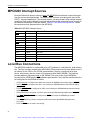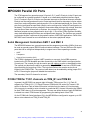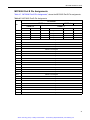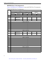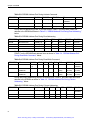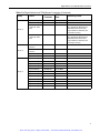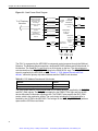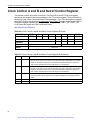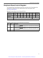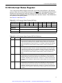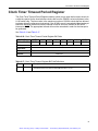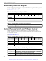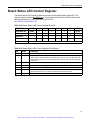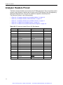
1
Artisan Technology Group is your source for quality new and certified-used/pre-owned equipment • FAST SHIPPING AND DELIVERY • TENS OF THOUSANDS OF IN-STOCK ITEMS • EQUIPMENT DEMOS • HUNDREDS OF MANUFACTURERS SUPPORTED • LEASING/MONTHLY RENTALS • ITAR CERTIFIED SECURE ASSET SOLUTIONS SERVICE CENTER REPAIRS Experienced engineers and technicians on staff at our full-service, in-house repair center WE BUY USED EQUIPMENT Sell your excess, underutilized, and idle used equipment We also offer credit for buy-backs and trade-ins www.artisantg.com/WeBuyEquipment InstraView REMOTE INSPECTION LOOKING FOR MORE INFORMATION? Visit us on the web at www.artisantg.com for more information on price quotations, drivers, technical specifications, manuals, and documentation SM Remotely inspect equipment before purchasing with our interactive website at www.instraview.com Contact us: (888) 88-SOURCE | [email protected] | www.artisantg.com PCI384 Four-Channel T1/ E1/J1 Telecom Adapter PCI384 Four-Channel T1/E1/J1 Telecom Adapter Hardware Manual Performance Technologies 205 Indigo Creek Drive Rochester, NY 14626 USA 585.256.0248 [email protected] www.pt.com © 2009 Performance Technologies, Inc. All Rights Reserved. Artisan Technology Group - Quality Instrumentation ... Guaranteed | (888) 88-SOURCE | www.artisantg.com Document Revision History Part Number Date Explanation of changes 126P0398.10 02/07/02 Initial Release 126P0398.11 04/26/02 Updates to Front Section 126P0398.20 11/02/09 Increased application Flash memory from 16 MB to 32 MB, see pages 25 and 118. Revised QuadFALC from Version 2.1 to Version 3.1, see pages 24 and 73. Moved certifications information and agency approvals to Appendix A, “Agency Approvals” on page 127. Renamed manual to match product name. Reformatted manual. Disclaimer This document presents information for users of Performance Technologies Inc. products. Although the information contained within this document is considered accurate and characteristic of the subject product, Performance Technologies Inc. reserves the right to make changes to this document and any products described herein to improve reliability, functionality, or design. Performance Technologies Inc. does not assume any liability arising out of the application or use of any product or circuit described herein. No part of this document may be copied or reproduced in any form or by any means without the prior permission of Performance Technologies Inc. Copyright Notice © Copyright 2009 by Performance Technologies, Inc. All Rights Reserved. The Performance Technologies logo is a registered trademark of Performance Technologies, Inc. All other product and brand names may be trademarks or registered trademarks of their respective owners. This document is the sole property of Performance Technologies Inc. Errors and Omissions Although diligent efforts are made to supply accurate technical information to the user, occasionally errors and omissions occur in manuals of this type. Refer to the Performance Technologies, Inc. Web site to obtain manual revisions or current customer information: http://www.pt.com. Performance Technologies, Inc., reserves its right to change product specifications without notice. Symbols and Conventions in this Manual An overbar indicates the signal is an Active Low signal. Example: ENUM The following symbols appear in this document. Caution: There is risk of personal injury or equipment damage. Follow the instructions. 2 Artisan Technology Group - Quality Instrumentation ... Guaranteed | (888) 88-SOURCE | www.artisantg.com Warning: Hazardous voltages are present. To reduce the risk of electrical shock and danger to personal health, follow the instructions. 3 Artisan Technology Group - Quality Instrumentation ... Guaranteed | (888) 88-SOURCE | www.artisantg.com 4 Artisan Technology Group - Quality Instrumentation ... Guaranteed | (888) 88-SOURCE | www.artisantg.com Contents Chapter 1: About This Guide 17 Overview . . . . . . . . . . . . . . . . . . . . . . . . . . . . . . . . . . . . . . . . . . . . . . . . . . . . . . . . . . . . . . . . . . . . 17 Text Conventions . . . . . . . . . . . . . . . . . . . . . . . . . . . . . . . . . . . . . . . . . . . . . . . . . . . . . . . . . . . . . 18 Customer Support and Services . . . . . . . . . . . . . . . . . . . . . . . . . . . . . . . . . . . . . . . . . . . . . . . . . . 18 Customer Support Packages . . . . . . . . . . . . . . . . . . . . . . . . . . . . . . . . . . . . . . . . . . . . . . . . . 19 Other Web Support . . . . . . . . . . . . . . . . . . . . . . . . . . . . . . . . . . . . . . . . . . . . . . . . . . . . . . . . . 19 Return Merchandise Authorization (RMA) . . . . . . . . . . . . . . . . . . . . . . . . . . . . . . . . . . . . . . . 19 Product Warranty . . . . . . . . . . . . . . . . . . . . . . . . . . . . . . . . . . . . . . . . . . . . . . . . . . . . . . . . . . . . . 19 Chapter 2: Introduction 21 Overview . . . . . . . . . . . . . . . . . . . . . . . . . . . . . . . . . . . . . . . . . . . . . . . . . . . . . . . . . . . . . . . . . . . . 21 Scope of this Document . . . . . . . . . . . . . . . . . . . . . . . . . . . . . . . . . . . . . . . . . . . . . . . . . . . . . . . . 21 PCI384 Models and Accessories . . . . . . . . . . . . . . . . . . . . . . . . . . . . . . . . . . . . . . . . . . . . . . . . . 22 Product Summary . . . . . . . . . . . . . . . . . . . . . . . . . . . . . . . . . . . . . . . . . . . . . . . . . . . . . . . . . . . . . 22 PCI384 Features . . . . . . . . . . . . . . . . . . . . . . . . . . . . . . . . . . . . . . . . . . . . . . . . . . . . . . . . . . . . . . 24 PCI384 Specifications . . . . . . . . . . . . . . . . . . . . . . . . . . . . . . . . . . . . . . . . . . . . . . . . . . . . . . . . . . 25 Additional Documentation . . . . . . . . . . . . . . . . . . . . . . . . . . . . . . . . . . . . . . . . . . . . . . . . . . . . . . . 25 Processor . . . . . . . . . . . . . . . . . . . . . . . . . . . . . . . . . . . . . . . . . . . . . . . . . . . . . . . . . . . . . . . . 25 PowerSpan PowerPC-to-PCI Bus Switch . . . . . . . . . . . . . . . . . . . . . . . . . . . . . . . . . . . . . . . . 26 QuadFALC Framer and Line Interface Component . . . . . . . . . . . . . . . . . . . . . . . . . . . . . . . . 26 H.100 WAN Access Switch . . . . . . . . . . . . . . . . . . . . . . . . . . . . . . . . . . . . . . . . . . . . . . . . . . . 26 Application Flash Memory . . . . . . . . . . . . . . . . . . . . . . . . . . . . . . . . . . . . . . . . . . . . . . . . . . . . 26 PICMG Specification . . . . . . . . . . . . . . . . . . . . . . . . . . . . . . . . . . . . . . . . . . . . . . . . . . . . . . . . 26 5 Artisan Technology Group - Quality Instrumentation ... Guaranteed | (888) 88-SOURCE | www.artisantg.com Contents Chapter 3: Installation 27 Overview . . . . . . . . . . . . . . . . . . . . . . . . . . . . . . . . . . . . . . . . . . . . . . . . . . . . . . . . . . . . . . . . . . . . 27 Installation Overview . . . . . . . . . . . . . . . . . . . . . . . . . . . . . . . . . . . . . . . . . . . . . . . . . . . . . . . . . . . 27 Handling Instructions . . . . . . . . . . . . . . . . . . . . . . . . . . . . . . . . . . . . . . . . . . . . . . . . . . . . . . . . . . 28 Configuration Jumpers . . . . . . . . . . . . . . . . . . . . . . . . . . . . . . . . . . . . . . . . . . . . . . . . . . . . . . . . . 28 Quick Installation . . . . . . . . . . . . . . . . . . . . . . . . . . . . . . . . . . . . . . . . . . . . . . . . . . . . . . . . . . . . . . 29 Standard Installation . . . . . . . . . . . . . . . . . . . . . . . . . . . . . . . . . . . . . . . . . . . . . . . . . . . . . . . . . . . 30 Chapter 4: Functional Description 33 Overview . . . . . . . . . . . . . . . . . . . . . . . . . . . . . . . . . . . . . . . . . . . . . . . . . . . . . . . . . . . . . . . . . . . . 33 PCI384 Product Description . . . . . . . . . . . . . . . . . . . . . . . . . . . . . . . . . . . . . . . . . . . . . . . . . . . . . 34 PCI384 Functional Block Diagram . . . . . . . . . . . . . . . . . . . . . . . . . . . . . . . . . . . . . . . . . . . . . . . . 34 Reset Logic . . . . . . . . . . . . . . . . . . . . . . . . . . . . . . . . . . . . . . . . . . . . . . . . . . . . . . . . . . . . . . . . . . 36 Power-on Reset . . . . . . . . . . . . . . . . . . . . . . . . . . . . . . . . . . . . . . . . . . . . . . . . . . . . . . . . . . . 36 Soft Reset . . . . . . . . . . . . . . . . . . . . . . . . . . . . . . . . . . . . . . . . . . . . . . . . . . . . . . . . . . . . . . . . 36 Tundra PowerSpan Resets . . . . . . . . . . . . . . . . . . . . . . . . . . . . . . . . . . . . . . . . . . . . . . . . . . . 37 Peripheral Resets . . . . . . . . . . . . . . . . . . . . . . . . . . . . . . . . . . . . . . . . . . . . . . . . . . . . . . . . . . 37 Central Processing Unit . . . . . . . . . . . . . . . . . . . . . . . . . . . . . . . . . . . . . . . . . . . . . . . . . . . . . . . . 38 MPC8260 Initial Configuration . . . . . . . . . . . . . . . . . . . . . . . . . . . . . . . . . . . . . . . . . . . . . . . . 38 Internal Initial Configuration . . . . . . . . . . . . . . . . . . . . . . . . . . . . . . . . . . . . . . . . . . . . . . . . . . . . . 39 Memory Map . . . . . . . . . . . . . . . . . . . . . . . . . . . . . . . . . . . . . . . . . . . . . . . . . . . . . . . . . . . . . . . . . 40 60x Bus Connections . . . . . . . . . . . . . . . . . . . . . . . . . . . . . . . . . . . . . . . . . . . . . . . . . . . . . . . . . . 41 MPC8260 Interrupt Sources . . . . . . . . . . . . . . . . . . . . . . . . . . . . . . . . . . . . . . . . . . . . . . . . . . . . . 42 Local Bus Connections . . . . . . . . . . . . . . . . . . . . . . . . . . . . . . . . . . . . . . . . . . . . . . . . . . . . . . . . . 42 MPC8260 Parallel I/O Ports . . . . . . . . . . . . . . . . . . . . . . . . . . . . . . . . . . . . . . . . . . . . . . . . . . . . . 43 Serial Management Controllers SMC 1 and SMC 2 . . . . . . . . . . . . . . . . . . . . . . . . . . . . . . . . 43 PCI384 TDM for T1/E1 channels on TDM_B1 and TDM B2 . . . . . . . . . . . . . . . . . . . . . . . . . . 43 MPC8260 Parallel Port Pin Assignments . . . . . . . . . . . . . . . . . . . . . . . . . . . . . . . . . . . . . . . . 44 JTAG Support . . . . . . . . . . . . . . . . . . . . . . . . . . . . . . . . . . . . . . . . . . . . . . . . . . . . . . . . . . . . . . . . 48 Chapter 5: SDRAM 49 Overview . . . . . . . . . . . . . . . . . . . . . . . . . . . . . . . . . . . . . . . . . . . . . . . . . . . . . . . . . . . . . . . . . . . . 49 Memory Organization . . . . . . . . . . . . . . . . . . . . . . . . . . . . . . . . . . . . . . . . . . . . . . . . . . . . . . . . . . 51 External Master Support . . . . . . . . . . . . . . . . . . . . . . . . . . . . . . . . . . . . . . . . . . . . . . . . . . . . . . . . 53 SDRAM Controller Initialization . . . . . . . . . . . . . . . . . . . . . . . . . . . . . . . . . . . . . . . . . . . . . . . . . . . 54 MPC8260 MPTPR and PSRT Register Configuration . . . . . . . . . . . . . . . . . . . . . . . . . . . . . . . . . 54 6 Artisan Technology Group - Quality Instrumentation ... Guaranteed | (888) 88-SOURCE | www.artisantg.com Contents MPC8260 PSDMR Register Configuration . . . . . . . . . . . . . . . . . . . . . . . . . . . . . . . . . . . . . . . 54 MPC8260 OR Register Configuration . . . . . . . . . . . . . . . . . . . . . . . . . . . . . . . . . . . . . . . . . . . 55 MPC8260 BR Register Configuration . . . . . . . . . . . . . . . . . . . . . . . . . . . . . . . . . . . . . . . . . . . 56 SDRAM Initialization Requirements . . . . . . . . . . . . . . . . . . . . . . . . . . . . . . . . . . . . . . . . . . . . 56 COMMAND INHIBIT . . . . . . . . . . . . . . . . . . . . . . . . . . . . . . . . . . . . . . . . . . . . . . . . . . . . . . . . 56 PRECHARGE . . . . . . . . . . . . . . . . . . . . . . . . . . . . . . . . . . . . . . . . . . . . . . . . . . . . . . . . . . . . . 57 AUTO REFRESH . . . . . . . . . . . . . . . . . . . . . . . . . . . . . . . . . . . . . . . . . . . . . . . . . . . . . . . . . . 57 SDRAM Mode Register Configuration . . . . . . . . . . . . . . . . . . . . . . . . . . . . . . . . . . . . . . . . . . 57 Chapter 6: TDM Clocking 59 Overview . . . . . . . . . . . . . . . . . . . . . . . . . . . . . . . . . . . . . . . . . . . . . . . . . . . . . . . . . . . . . . . . . . . . 59 H.100 DPLL . . . . . . . . . . . . . . . . . . . . . . . . . . . . . . . . . . . . . . . . . . . . . . . . . . . . . . . . . . . . . . . . . 60 Internal Reference Clock Sources . . . . . . . . . . . . . . . . . . . . . . . . . . . . . . . . . . . . . . . . . . . . . . . . 61 Internal Reference Monitors . . . . . . . . . . . . . . . . . . . . . . . . . . . . . . . . . . . . . . . . . . . . . . . . . . . . . 61 CT Clock and Frame Monitor Circuits . . . . . . . . . . . . . . . . . . . . . . . . . . . . . . . . . . . . . . . . . . . . . . 61 External Reference Clock Sources . . . . . . . . . . . . . . . . . . . . . . . . . . . . . . . . . . . . . . . . . . . . . . . . 61 External Reference Clock Source Monitor . . . . . . . . . . . . . . . . . . . . . . . . . . . . . . . . . . . . . . . . . . 62 H.100 Clock Operating Modes . . . . . . . . . . . . . . . . . . . . . . . . . . . . . . . . . . . . . . . . . . . . . . . . . . . 62 CT Netreference Sources . . . . . . . . . . . . . . . . . . . . . . . . . . . . . . . . . . . . . . . . . . . . . . . . . . . . 62 Chapter 7: H.100 Bus and Digital Switch 65 Overview . . . . . . . . . . . . . . . . . . . . . . . . . . . . . . . . . . . . . . . . . . . . . . . . . . . . . . . . . . . . . . . . . . . . 65 H.100 Bus and Digital Switch Features . . . . . . . . . . . . . . . . . . . . . . . . . . . . . . . . . . . . . . . . . . . . 65 General Description . . . . . . . . . . . . . . . . . . . . . . . . . . . . . . . . . . . . . . . . . . . . . . . . . . . . . . . . . . . 66 MPC8260 Related H.100 Settings . . . . . . . . . . . . . . . . . . . . . . . . . . . . . . . . . . . . . . . . . . . . . . . . 68 Digital Switch Local TDM Streams Connection . . . . . . . . . . . . . . . . . . . . . . . . . . . . . . . . . . . . . . 70 Chapter 8: T1/E1/J1 Quad Framer and LIU 73 Overview . . . . . . . . . . . . . . . . . . . . . . . . . . . . . . . . . . . . . . . . . . . . . . . . . . . . . . . . . . . . . . . . . . . . 73 QuadFALC Features . . . . . . . . . . . . . . . . . . . . . . . . . . . . . . . . . . . . . . . . . . . . . . . . . . . . . . . . . . . 73 Frame Aligner Features . . . . . . . . . . . . . . . . . . . . . . . . . . . . . . . . . . . . . . . . . . . . . . . . . . . . . 74 Signaling Controller Features . . . . . . . . . . . . . . . . . . . . . . . . . . . . . . . . . . . . . . . . . . . . . . . . . 75 General Features . . . . . . . . . . . . . . . . . . . . . . . . . . . . . . . . . . . . . . . . . . . . . . . . . . . . . . . . . . 75 MPC8260 Related FALC Settings . . . . . . . . . . . . . . . . . . . . . . . . . . . . . . . . . . . . . . . . . . . . . . . . 77 Quad Framers and LIUs Register Map . . . . . . . . . . . . . . . . . . . . . . . . . . . . . . . . . . . . . . . . . . . . . 77 Quad Framers and LIUs Physical Configuration . . . . . . . . . . . . . . . . . . . . . . . . . . . . . . . . . . . . . . 77 Line Interface Receive Configuration . . . . . . . . . . . . . . . . . . . . . . . . . . . . . . . . . . . . . . . . . . . 78 7 Artisan Technology Group - Quality Instrumentation ... Guaranteed | (888) 88-SOURCE | www.artisantg.com Contents Line Interface Transmit Configuration . . . . . . . . . . . . . . . . . . . . . . . . . . . . . . . . . . . . . . . . . . . 78 Master Clock Configuration . . . . . . . . . . . . . . . . . . . . . . . . . . . . . . . . . . . . . . . . . . . . . . . . . . . 78 External DCO-R Clock SYNC Pin Configuration . . . . . . . . . . . . . . . . . . . . . . . . . . . . . . . . . . 78 One Second Timer Pin Configuration . . . . . . . . . . . . . . . . . . . . . . . . . . . . . . . . . . . . . . . . . . . 78 Line Receive Clock Output Pin Configuration . . . . . . . . . . . . . . . . . . . . . . . . . . . . . . . . . . . . . 78 Local TDM Receive Data Pin Configuration . . . . . . . . . . . . . . . . . . . . . . . . . . . . . . . . . . . . . . 79 Local TDM Receive System Clock Pin Configuration . . . . . . . . . . . . . . . . . . . . . . . . . . . . . . . 79 Local TDM Receive Frame Pulse Input Pin Configuration . . . . . . . . . . . . . . . . . . . . . . . . . . . 79 Receive Channel Associated Signaling . . . . . . . . . . . . . . . . . . . . . . . . . . . . . . . . . . . . . . . . . 79 Local TDM Transmit Data Pin Configuration . . . . . . . . . . . . . . . . . . . . . . . . . . . . . . . . . . . . . 79 Local TDM Transmit Channel Associated Signaling Pin Configuration . . . . . . . . . . . . . . . . . 80 Local TDM Transmit System Clock Pin Configuration . . . . . . . . . . . . . . . . . . . . . . . . . . . . . . 80 Local TDM Transmit Frame Pulse Input Pin Configuration . . . . . . . . . . . . . . . . . . . . . . . . . . . 80 Line Side T1 Transmit Clock Source . . . . . . . . . . . . . . . . . . . . . . . . . . . . . . . . . . . . . . . . . . . 80 QuadFALC Interrupts . . . . . . . . . . . . . . . . . . . . . . . . . . . . . . . . . . . . . . . . . . . . . . . . . . . . . . . 81 Transmitter Line Termination and Conditioning . . . . . . . . . . . . . . . . . . . . . . . . . . . . . . . . . . . . . . 81 Receiver Line Termination and Conditioning . . . . . . . . . . . . . . . . . . . . . . . . . . . . . . . . . . . . . . . . 81 Chapter 9: General Purpose Registers 83 Overview . . . . . . . . . . . . . . . . . . . . . . . . . . . . . . . . . . . . . . . . . . . . . . . . . . . . . . . . . . . . . . . . . . . . 83 PSM518 and PSM520 General Purpose Registers . . . . . . . . . . . . . . . . . . . . . . . . . . . . . . . . . . . 86 LREF0 and LREF1 Select Register . . . . . . . . . . . . . . . . . . . . . . . . . . . . . . . . . . . . . . . . . . . . . . . 87 Clock Control A and B and Netref Control Register . . . . . . . . . . . . . . . . . . . . . . . . . . . . . . . . . . . 88 Peripheral Reset Control Register . . . . . . . . . . . . . . . . . . . . . . . . . . . . . . . . . . . . . . . . . . . . . . . . 89 H.100 Peripheral Interrupt Enable Control Register . . . . . . . . . . . . . . . . . . . . . . . . . . . . . . . . . . . 90 H.100 Interrupt Status Register . . . . . . . . . . . . . . . . . . . . . . . . . . . . . . . . . . . . . . . . . . . . . . . . . . 91 Miscellaneous Status and Control Register . . . . . . . . . . . . . . . . . . . . . . . . . . . . . . . . . . . . . . . . . 92 Clock Timer Timeout Period Register . . . . . . . . . . . . . . . . . . . . . . . . . . . . . . . . . . . . . . . . . . . . . . 93 General Purpose Latch Register . . . . . . . . . . . . . . . . . . . . . . . . . . . . . . . . . . . . . . . . . . . . . . . . . . 94 General Purpose Switch and P1 Reset Register . . . . . . . . . . . . . . . . . . . . . . . . . . . . . . . . . . . . . 94 LREF3 Select Register . . . . . . . . . . . . . . . . . . . . . . . . . . . . . . . . . . . . . . . . . . . . . . . . . . . . . . . . . 95 Board ID Register . . . . . . . . . . . . . . . . . . . . . . . . . . . . . . . . . . . . . . . . . . . . . . . . . . . . . . . . . . . . . 96 Board Option and Revision Register . . . . . . . . . . . . . . . . . . . . . . . . . . . . . . . . . . . . . . . . . . . . . . . 96 General Purpose Switch and H.100 Termination Register . . . . . . . . . . . . . . . . . . . . . . . . . . . . . . 97 H.100 Digital Switch Clock Control . . . . . . . . . . . . . . . . . . . . . . . . . . . . . . . . . . . . . . . . . . . . . . . . 98 Board Status LED Control Register . . . . . . . . . . . . . . . . . . . . . . . . . . . . . . . . . . . . . . . . . . . . . . . 99 8 Artisan Technology Group - Quality Instrumentation ... Guaranteed | (888) 88-SOURCE | www.artisantg.com Contents General Purpose Switch . . . . . . . . . . . . . . . . . . . . . . . . . . . . . . . . . . . . . . . . . . . . . . . . . . . . . . . 100 Receiver Termination Control Register . . . . . . . . . . . . . . . . . . . . . . . . . . . . . . . . . . . . . . . . . . . . 101 Transmitter Termination Control Register . . . . . . . . . . . . . . . . . . . . . . . . . . . . . . . . . . . . . . . . . . 102 Chapter 10: Pinouts 103 Overview . . . . . . . . . . . . . . . . . . . . . . . . . . . . . . . . . . . . . . . . . . . . . . . . . . . . . . . . . . . . . . . . . . . 103 PCI Pin Assignments . . . . . . . . . . . . . . . . . . . . . . . . . . . . . . . . . . . . . . . . . . . . . . . . . . . . . . . . . 104 Modular Jack Pin Assignments . . . . . . . . . . . . . . . . . . . . . . . . . . . . . . . . . . . . . . . . . . . . . . . . . . 107 Master/Slave PCM Expansion Connector Pin Assignments . . . . . . . . . . . . . . . . . . . . . . . . . . . . 108 JTAG/BDM Debug Port . . . . . . . . . . . . . . . . . . . . . . . . . . . . . . . . . . . . . . . . . . . . . . . . . . . . . . . . 109 Analyzer Headers Pinout . . . . . . . . . . . . . . . . . . . . . . . . . . . . . . . . . . . . . . . . . . . . . . . . . . . . . . 110 P4 Nine-Pin D Subminiature Connector Pinout . . . . . . . . . . . . . . . . . . . . . . . . . . . . . . . . . . . . . 113 P3 Board Configuration Header . . . . . . . . . . . . . . . . . . . . . . . . . . . . . . . . . . . . . . . . . . . . . . . . . 113 Chapter 11: Memory 115 Overview . . . . . . . . . . . . . . . . . . . . . . . . . . . . . . . . . . . . . . . . . . . . . . . . . . . . . . . . . . . . . . . . . . . 115 Boot Flash Memory . . . . . . . . . . . . . . . . . . . . . . . . . . . . . . . . . . . . . . . . . . . . . . . . . . . . . . . . . . . 116 MPC8260 Related Flash Settings - CS0 . . . . . . . . . . . . . . . . . . . . . . . . . . . . . . . . . . . . . . . . . . . 117 General Flash Information . . . . . . . . . . . . . . . . . . . . . . . . . . . . . . . . . . . . . . . . . . . . . . . . . . . . . 118 Application Flash Memory . . . . . . . . . . . . . . . . . . . . . . . . . . . . . . . . . . . . . . . . . . . . . . . . . . . . . . 118 MPC8260 Related Flash Settings - CS3 . . . . . . . . . . . . . . . . . . . . . . . . . . . . . . . . . . . . . . . . . . . 120 General Application Flash Information . . . . . . . . . . . . . . . . . . . . . . . . . . . . . . . . . . . . . . . . . . . . 120 Communications Buffer Memory . . . . . . . . . . . . . . . . . . . . . . . . . . . . . . . . . . . . . . . . . . . . . . . . . 121 MPC8260 Related Communications Buffer Memory Settings . . . . . . . . . . . . . . . . . . . . . . . . . . 122 UPMB Table Settings . . . . . . . . . . . . . . . . . . . . . . . . . . . . . . . . . . . . . . . . . . . . . . . . . . . . . . . . . 123 PCI Interface . . . . . . . . . . . . . . . . . . . . . . . . . . . . . . . . . . . . . . . . . . . . . . . . . . . . . . . . . . . . . . . . 123 PowerSpan Signal Connections and Hardware Configuration . . . . . . . . . . . . . . . . . . . . . . . . . . 123 PowerSpan Reset Configuration Word . . . . . . . . . . . . . . . . . . . . . . . . . . . . . . . . . . . . . . . . . . . . 124 Local Processor Connections Between MPC8260 and PowerSpan . . . . . . . . . . . . . . . . . . . . . . 125 PowerSpan Interrupts . . . . . . . . . . . . . . . . . . . . . . . . . . . . . . . . . . . . . . . . . . . . . . . . . . . . . . . . . 126 Appendix A: Agency Approvals 127 Overview . . . . . . . . . . . . . . . . . . . . . . . . . . . . . . . . . . . . . . . . . . . . . . . . . . . . . . . . . . . . . . . . . . . 127 CE Certification . . . . . . . . . . . . . . . . . . . . . . . . . . . . . . . . . . . . . . . . . . . . . . . . . . . . . . . . . . . . . . 128 FCC (USA) Class A Notice . . . . . . . . . . . . . . . . . . . . . . . . . . . . . . . . . . . . . . . . . . . . . . . . . . . . . 128 Industry Canada Class A Notice . . . . . . . . . . . . . . . . . . . . . . . . . . . . . . . . . . . . . . . . . . . . . . . . . 129 Safety Information . . . . . . . . . . . . . . . . . . . . . . . . . . . . . . . . . . . . . . . . . . . . . . . . . . . . . . . . . . . . 129 9 Artisan Technology Group - Quality Instrumentation ... Guaranteed | (888) 88-SOURCE | www.artisantg.com Contents Safety Precautions . . . . . . . . . . . . . . . . . . . . . . . . . . . . . . . . . . . . . . . . . . . . . . . . . . . . . . . . 129 Compliance with RoHS and WEEE Directives . . . . . . . . . . . . . . . . . . . . . . . . . . . . . . . . . . . . . . 130 10 Artisan Technology Group - Quality Instrumentation ... Guaranteed | (888) 88-SOURCE | www.artisantg.com Ta b l e s Table 2-1: PCI384 Part Numbers . . . . . . . . . . . . . . . . . . . . . . . . . . . . . . . . . . . . . . . . . . . . . . . . . . . . 22 Table 2-2: PCI384 Specifications . . . . . . . . . . . . . . . . . . . . . . . . . . . . . . . . . . . . . . . . . . . . . . . . . . . . 25 Table 3-1: Configuration Jumpers . . . . . . . . . . . . . . . . . . . . . . . . . . . . . . . . . . . . . . . . . . . . . . . . . . . . 29 Table 4-1: Peripheral Resets . . . . . . . . . . . . . . . . . . . . . . . . . . . . . . . . . . . . . . . . . . . . . . . . . . . . . . . . 37 Table 4-2: System Clock Control Register Bit Field Definitions . . . . . . . . . . . . . . . . . . . . . . . . . . . . . . 38 Table 4-3: SIUMCR Register Settings . . . . . . . . . . . . . . . . . . . . . . . . . . . . . . . . . . . . . . . . . . . . . . . . . 39 Table 4-4: MPC8269 Chip Select Assignments. . . . . . . . . . . . . . . . . . . . . . . . . . . . . . . . . . . . . . . . . . 41 Table 4-5: MPC8260 Interrupt Source. . . . . . . . . . . . . . . . . . . . . . . . . . . . . . . . . . . . . . . . . . . . . . . . . 42 Table 4-6: MPC8260 Port A Pin Assignments. . . . . . . . . . . . . . . . . . . . . . . . . . . . . . . . . . . . . . . . . . . 44 Table 4-7: MPC8260 Port B Pin Assignments. . . . . . . . . . . . . . . . . . . . . . . . . . . . . . . . . . . . . . . . . . . 45 Table 4-8: MPC8260 Port C Pin Assignments. . . . . . . . . . . . . . . . . . . . . . . . . . . . . . . . . . . . . . . . . . . 46 Table 4-9: MPC8260 Port D Pin Assignments. . . . . . . . . . . . . . . . . . . . . . . . . . . . . . . . . . . . . . . . . . . 47 Table 4-10: JTAG Pinouts . . . . . . . . . . . . . . . . . . . . . . . . . . . . . . . . . . . . . . . . . . . . . . . . . . . . . . . . . . 48 Table 5-1: 60x Address Bus Partitioning . . . . . . . . . . . . . . . . . . . . . . . . . . . . . . . . . . . . . . . . . . . . . . . 51 Table 5-2: SDRAM Address Port During Activate Command . . . . . . . . . . . . . . . . . . . . . . . . . . . . . . . 52 Table 5-3: SDRAM Address Port During Row Addressing . . . . . . . . . . . . . . . . . . . . . . . . . . . . . . . . . 52 Table 5-4: SDRAM Address Port During Read/Write Command. . . . . . . . . . . . . . . . . . . . . . . . . . . . . 52 Table 5-5: SDRAM Address Port During Column Addressing. . . . . . . . . . . . . . . . . . . . . . . . . . . . . . . 52 11 Artisan Technology Group - Quality Instrumentation ... Guaranteed | (888) 88-SOURCE | www.artisantg.com Tables Table 5-6: PSDMR Register Configuration . . . . . . . . . . . . . . . . . . . . . . . . . . . . . . . . . . . . . . . . . . . . . 54 Table 5-7: MPC8260 OR Register Configuration . . . . . . . . . . . . . . . . . . . . . . . . . . . . . . . . . . . . . . . . 55 Table 5-8: MPC8260 BR Register Configuration. . . . . . . . . . . . . . . . . . . . . . . . . . . . . . . . . . . . . . . . . 56 Table 6-1: H.100 DPLL Operating Specifications . . . . . . . . . . . . . . . . . . . . . . . . . . . . . . . . . . . . . . . . 60 Table 7-1: CS6 Base Register Settings . . . . . . . . . . . . . . . . . . . . . . . . . . . . . . . . . . . . . . . . . . . . . . . . 68 Table 7-2: CS6 Option Register Settings. . . . . . . . . . . . . . . . . . . . . . . . . . . . . . . . . . . . . . . . . . . . . . . 68 Table 7-3: H.100 Digital Switch Register Map . . . . . . . . . . . . . . . . . . . . . . . . . . . . . . . . . . . . . . . . . . . 69 Table 7-4: Digital Switch Local TDM Stream Connection . . . . . . . . . . . . . . . . . . . . . . . . . . . . . . . . . . 70 Table 8-1: CS5 Address Decode and Sub-decode . . . . . . . . . . . . . . . . . . . . . . . . . . . . . . . . . . . . . . . 76 Table 8-2: CS5 Base Register Settings . . . . . . . . . . . . . . . . . . . . . . . . . . . . . . . . . . . . . . . . . . . . . . . . 77 Table 8-3: CS5 Option Register Settings. . . . . . . . . . . . . . . . . . . . . . . . . . . . . . . . . . . . . . . . . . . . . . . 77 Table 9-1: CS4 Base Register Settings . . . . . . . . . . . . . . . . . . . . . . . . . . . . . . . . . . . . . . . . . . . . . . . . 84 Table 9-2: CS4 Option Register Settings. . . . . . . . . . . . . . . . . . . . . . . . . . . . . . . . . . . . . . . . . . . . . . . 85 Table 9-3: PSM518 and PSM520 General Purpose Registers . . . . . . . . . . . . . . . . . . . . . . . . . . . . . . 86 Table 9-4: LREF0 and LREF1 Register Bit Fields . . . . . . . . . . . . . . . . . . . . . . . . . . . . . . . . . . . . . . . . 87 Table 9-5: LREF0 and LREF1 Register Bit Field Definitions . . . . . . . . . . . . . . . . . . . . . . . . . . . . . . . . 87 Table 9-6: Clock Control A and B and Netref Control Register Bit Fields . . . . . . . . . . . . . . . . . . . . . . 88 Table 9-7: Clock Control A and B and Netref Control Register Bit Definitions . . . . . . . . . . . . . . . . . . 88 Table 9-8: Peripheral Reset Control Register Bit Fields . . . . . . . . . . . . . . . . . . . . . . . . . . . . . . . . . . . 89 Table 9-9: Peripheral Reset Control Register Bit Field Definitions . . . . . . . . . . . . . . . . . . . . . . . . . . . 89 Table 9-10: H.100 Peripheral Interrupt Enable Control Register Bit Fields . . . . . . . . . . . . . . . . . . . . . 90 Table 9-11: H.100 Peripheral Interrupt Enable Control Register Bit Field Definitions . . . . . . . . . . . . . 90 Table 9-12: H.100 Interrupt Status Register Bit Fields . . . . . . . . . . . . . . . . . . . . . . . . . . . . . . . . . . . . 91 Table 9-13: H.100 Interrupt Status Register Bit Field Definitions . . . . . . . . . . . . . . . . . . . . . . . . . . . . 91 Table 9-14: Miscellaneous Status and Control Register Bit Fields . . . . . . . . . . . . . . . . . . . . . . . . . . . 92 Table 9-15: Miscellaneous Status and Control Register Bit Field Definitions . . . . . . . . . . . . . . . . . . . 92 12 Artisan Technology Group - Quality Instrumentation ... Guaranteed | (888) 88-SOURCE | www.artisantg.com Tables Table 9-16: Clock Timer Timeout Period Register Bit Fields . . . . . . . . . . . . . . . . . . . . . . . . . . . . . . . . 93 Table 9-17: Clock Timer Timeout Register Bit Field Definitions . . . . . . . . . . . . . . . . . . . . . . . . . . . . . 93 Table 9-18: General Purpose Latch Register Bit Fields . . . . . . . . . . . . . . . . . . . . . . . . . . . . . . . . . . . 94 Table 9-19: General Purpose Latch Register Bit Field Definitions . . . . . . . . . . . . . . . . . . . . . . . . . . . 94 Table 9-20: General Purpose Switch and P1 Reset Register Bit Fields . . . . . . . . . . . . . . . . . . . . . . . 94 Table 9-21: General Purpose Switch and P1 Reset Register Bit Field Definitions . . . . . . . . . . . . . . . 94 Table 9-22: LREF3 Select Register Bit Fields . . . . . . . . . . . . . . . . . . . . . . . . . . . . . . . . . . . . . . . . . . . 95 Table 9-23: LREF3 Select Register Bit Field Definitions . . . . . . . . . . . . . . . . . . . . . . . . . . . . . . . . . . . 95 Table 9-24: Board ID Register Bit Fields . . . . . . . . . . . . . . . . . . . . . . . . . . . . . . . . . . . . . . . . . . . . . . . 96 Table 9-25: Board ID Register Bit Field Definitions . . . . . . . . . . . . . . . . . . . . . . . . . . . . . . . . . . . . . . . 96 Table 9-26: Board ID Register Bit Fields . . . . . . . . . . . . . . . . . . . . . . . . . . . . . . . . . . . . . . . . . . . . . . . 96 Table 9-27: Board ID Register Bit Field Definitions . . . . . . . . . . . . . . . . . . . . . . . . . . . . . . . . . . . . . . . 96 Table 9-28: General Purpose Switch and P1 Reset Register Bit Fields . . . . . . . . . . . . . . . . . . . . . . . 97 Table 9-29: General Purpose Switch and P1 Reset Register Bit Field Definitions . . . . . . . . . . . . . . . 97 Table 9-30: Zarlink Patch Control Register Bit Fields . . . . . . . . . . . . . . . . . . . . . . . . . . . . . . . . . . . . . 98 Table 9-31: Zarlink Patch Control Register Bit Field Definitions . . . . . . . . . . . . . . . . . . . . . . . . . . . . . 98 Table 9-32: Board Status LED Control Register Bit Fields . . . . . . . . . . . . . . . . . . . . . . . . . . . . . . . . . 99 Table 9-33: Board Status LED Control Register Bit Definitions . . . . . . . . . . . . . . . . . . . . . . . . . . . . . . 99 Table 9-34: General Purpose Switch and P1 Reset Register Bit Fields . . . . . . . . . . . . . . . . . . . . . . 100 Table 9-35: General Purpose Switch and P1 Reset Register Bit Field Definitions . . . . . . . . . . . . . . 100 Table 9-36: Receiver Termination Control Register Bit Fields. . . . . . . . . . . . . . . . . . . . . . . . . . . . . . 101 Table 9-37: Receiver Termination Control Register Bit Field Definitions. . . . . . . . . . . . . . . . . . . . . . 101 Table 9-38: Transmitter Termination Control Register Bit Fields. . . . . . . . . . . . . . . . . . . . . . . . . . . . 102 Table 9-39: Transmitter Termination Control Register Bit Field Definition . . . . . . . . . . . . . . . . . . . . 102 Table 10-1: Base P1 PCI Connector . . . . . . . . . . . . . . . . . . . . . . . . . . . . . . . . . . . . . . . . . . . . . . . . . 104 Table 10-2: Mezzanine J1 Telecom Line Interface . . . . . . . . . . . . . . . . . . . . . . . . . . . . . . . . . . . . . . 107 13 Artisan Technology Group - Quality Instrumentation ... Guaranteed | (888) 88-SOURCE | www.artisantg.com Tables Table 10-3: Mezzanine P2 Master/Slave PCM Expansion Connector . . . . . . . . . . . . . . . . . . . . . . . 108 Table 10-4: JTAG Pinouts . . . . . . . . . . . . . . . . . . . . . . . . . . . . . . . . . . . . . . . . . . . . . . . . . . . . . . . . . 109 Table 10-5: P5 Analyzer Header Pinout, 60X Bus Address . . . . . . . . . . . . . . . . . . . . . . . . . . . . . . . 110 Table 10-6: P8 Analyzer Header, 60X Bus MS Data. . . . . . . . . . . . . . . . . . . . . . . . . . . . . . . . . . . . . 111 Table 10-7: P9 Analyzer Header Pinout, 60X Bus LS Data. . . . . . . . . . . . . . . . . . . . . . . . . . . . . . . . 111 Table 10-8: P7 Mictor Pinout, 60X Bus Control . . . . . . . . . . . . . . . . . . . . . . . . . . . . . . . . . . . . . . . . . 112 Table 10-9: P6 Mictor Pinout, 60X Bus Miscellaneous Signals . . . . . . . . . . . . . . . . . . . . . . . . . . . . . 112 Table 10-10: P4 Nine-Pin D Subminiature Pinout . . . . . . . . . . . . . . . . . . . . . . . . . . . . . . . . . . . . . . . 113 Table 10-11: P3 Header Pinout . . . . . . . . . . . . . . . . . . . . . . . . . . . . . . . . . . . . . . . . . . . . . . . . . . . . . 113 Table 11-1: CS0 Base Register Settings . . . . . . . . . . . . . . . . . . . . . . . . . . . . . . . . . . . . . . . . . . . . . . 117 Table 11-2: CS0 Option Register Settings. . . . . . . . . . . . . . . . . . . . . . . . . . . . . . . . . . . . . . . . . . . . . 117 Table 11-3: CS3 Base Register Settings . . . . . . . . . . . . . . . . . . . . . . . . . . . . . . . . . . . . . . . . . . . . . . 120 Table 11-4: CS3 Option Register Settings. . . . . . . . . . . . . . . . . . . . . . . . . . . . . . . . . . . . . . . . . . . . . 120 Table 11-5: CS2 Base Register Settings . . . . . . . . . . . . . . . . . . . . . . . . . . . . . . . . . . . . . . . . . . . . . . 122 Table 11-6: CS2 Option Register Settings. . . . . . . . . . . . . . . . . . . . . . . . . . . . . . . . . . . . . . . . . . . . . 122 Table 11-7: Signal Variations Between PowerSpan and the MPC8260 . . . . . . . . . . . . . . . . . . . . . . 125 Table 11-8: PowerSpan Reset Pins. . . . . . . . . . . . . . . . . . . . . . . . . . . . . . . . . . . . . . . . . . . . . . . . . . 125 Table 11-9: PowerSpan Interrupt Connections . . . . . . . . . . . . . . . . . . . . . . . . . . . . . . . . . . . . . . . . . 126 14 Artisan Technology Group - Quality Instrumentation ... Guaranteed | (888) 88-SOURCE | www.artisantg.com Figures Figure 2-1: PCI384 Quad T1/E1/J1 Telecom Adapter. . . . . . . . . . . . . . . . . . . . . . . . . . . . . . . . . . . . . 23 Figure 3-1: Configuration Jumpers . . . . . . . . . . . . . . . . . . . . . . . . . . . . . . . . . . . . . . . . . . . . . . . . . . . 28 Figure 3-2: Stacked PCI384 Boards . . . . . . . . . . . . . . . . . . . . . . . . . . . . . . . . . . . . . . . . . . . . . . . . . . 31 Figure 4-1: PCI384 Block Diagram . . . . . . . . . . . . . . . . . . . . . . . . . . . . . . . . . . . . . . . . . . . . . . . . . . . 35 Figure 5-1: Partial FSDRAM State Diagram . . . . . . . . . . . . . . . . . . . . . . . . . . . . . . . . . . . . . . . . . . . . 50 Figure 5-2: External Master SDRAM Configuration . . . . . . . . . . . . . . . . . . . . . . . . . . . . . . . . . . . . . . . 53 Figure 6-1: TDM Clock Tree . . . . . . . . . . . . . . . . . . . . . . . . . . . . . . . . . . . . . . . . . . . . . . . . . . . . . . . . 63 Figure 7-1: H.100 Data and Control. . . . . . . . . . . . . . . . . . . . . . . . . . . . . . . . . . . . . . . . . . . . . . . . . . . 67 Figure 8-1: Quad Framer Block Diagram. . . . . . . . . . . . . . . . . . . . . . . . . . . . . . . . . . . . . . . . . . . . . . . 76 Figure 9-1: Miscellaneous Registers Block Diagram . . . . . . . . . . . . . . . . . . . . . . . . . . . . . . . . . . . . . . 84 Figure 11-1: Boot Flash Block Diagram. . . . . . . . . . . . . . . . . . . . . . . . . . . . . . . . . . . . . . . . . . . . . . . 116 Figure 11-2: Application Flash Block Diagram. . . . . . . . . . . . . . . . . . . . . . . . . . . . . . . . . . . . . . . . . . 119 Figure 11-3: Communications Buffer Memory Block Diagram. . . . . . . . . . . . . . . . . . . . . . . . . . . . . . 121 15 Artisan Technology Group - Quality Instrumentation ... Guaranteed | (888) 88-SOURCE | www.artisantg.com Figures 16 Artisan Technology Group - Quality Instrumentation ... Guaranteed | (888) 88-SOURCE | www.artisantg.com Chapter 1 About This Guide Overview This manual describes the operation and use of the PCI384 Four-Channel T1/E1/J1 Telecom Adapter (referred to as the PCI384 in this manual). The following outline describes the focus of each chapter. In these chapters you will find installation and configuration information, plus a functional block description intended for the application developer of this board. Here is a brief description of what you will find in this manual: Chapter 1, “About This Guide,” this chapter, provides links to all other chapters in this manual, customer support and services, and product warranty information for the PCI384. Chapter 2, “Introduction,” on page 21, introduces users to the PCI384 Four-Channel T1/E1/J1 Telecom Adapter and includes a product description, a list of product specifications, and links to related documents. Chapter 3, “Installation,” on page 27 describes how to handle, configure the jumpers and install the PCI384. Chapter 4, “Functional Description,” on page 33 provides an overview of the PCI384 and includes information such as module features, functional block diagram, and a brief description of each block. Chapter 5, “SDRAM,” on page 49 discusses SDRAM on the PCI384. Chapter 6, “TDM Clocking,” on page 59 discusses TDM clock distribution, which is centralized about the Zarlink MT90866 H.100 TDM switch on the PCI384. Chapter 7, “H.100 Bus and Digital Switch,” on page 65 discusses the Zarlink MT90866 switch found on the mezzanine I/O board on the PCI384. 17 Artisan Technology Group - Quality Instrumentation ... Guaranteed | (888) 88-SOURCE | www.artisantg.com Chapter 1: About This Guide Chapter 8, “T1/E1/J1 Quad Framer and LIU,” on page 73 discusses the T1/E1/J1 quad framer with integral line interface unit found on the mezzanine I/O board on the PCI384. Chapter 9, “General Purpose Registers,” on page 83 describes the programmable General Purpose Control and Status Registers used to configure and monitor PCI384 functionality. Chapter 10, “Pinouts,” on page 103 present the pin assignments for the PCI384. Chapter 11, “Memory,” on page 115 discusses the various memory components and settings on the PCI384. Appendix A, “Agency Approvals” on page 127 presents agency approval and certification information. The most current documentation to support any additional components that you purchased from Performance Technologies is available at www.pt.com under the product you are inquiring about. Text Conventions This manual uses the following conventions: Convention Used For Monospace font Monospace font represents sample code. Bold font Bold font represents: • Paths • File names • UNIX commands • User input Italic font Italic font represents: • Notes that supply useful advice • Supplemental information • Referenced documents Overline An overline is used to represent an Active Low signal. Regular font Regular font is used for the ENTER and TAB keys and the SPACEBAR on your keyboard. Customer Support and Services Performance Technologies offers a variety of standard and custom support packages to ensure customers have access to the critical resources that they need to protect and maximize hardware and software investments throughout the development, integration, and deployment phases of the product life cycle. If you encounter difficulty in using this Performance Technologies, Inc. product, you may contact our support personnel by: 1. EMAIL (Preferred Method) – Email us at the addresses listed below or use our online email support form. Outline your problem in detail. Please include your return email address and a telephone number. 2. TELEPHONE – Contact us via telephone at the number listed below, and request Technical Support. 18 Artisan Technology Group - Quality Instrumentation ... Guaranteed | (888) 88-SOURCE | www.artisantg.com Product Warranty Our offices are open Monday to Friday, 8:00 a.m. to 8:00 p.m. (Eastern Standard Time). Performance Technologies Support Contact Information Embedded Systems and Software (Includes Platforms, Blades, and Servers) SS7 Systems (Includes SEGway™) Email [email protected] [email protected] Phone +1 (585) 256-0248 (Monday to Friday, 8 a.m. to 8 p.m. Eastern Standard Time) +1 (585) 256-0248 (Monday to Friday, 8 a.m. to 8 p.m. Eastern Standard Time) If you are located outside North America, we encourage you to contact the local Performance Technologies’ distributor or agent for support. Many of our distributors or agents maintain technical support staffs. Customer Support Packages Our configurable development and integration support packages help customers maximize engineering efforts and achieve time-to-market goals. To find out more about our Customer Support packages, visit http://www.pt.com/page/support/. Other Web Support Support for existing products including manuals, release notes, and drivers can be found on specific product pages at http://www.pt.com. Use the product search to locate the information you need. Return Merchandise Authorization (RMA) To submit a return merchandise authorization (RMA) request, complete the online RMA form available at http://pt.com/assets/lib/files/rma-request-form.doc and follow the instructions on the form. You will be notified with an RMA number once your return request is approved. Shipping information for returning the unit to Performance Technologies will be provided once the RMA is issued. Product Warranty Performance Technologies, Incorporated, warrants that its products sold hereunder will at the time of shipment be free from defects in material and workmanship and will conform to Performance Technologies’ applicable specifications or, if appropriate, to Buyer’s specifications accepted by Performance Technologies in writing. If products sold hereunder are not as warranted, Performance Technologies shall, at its option, refund the purchase price, repair, or replace the product provided proof of purchase and written notice of nonconformance are received by Performance Technologies within 12 months of shipment, or in the case of software and integrated circuits within ninety (90) days of shipment and provided said nonconforming products are returned F.O.B. to Performance Technologies’s facility no later than thirty days after the warranty period expires. Products returned under warranty claims must be accompanied by an approved Return Material Authorization number issued by Performance Technologies and a statement of the reason for the return. Please contact Performance Technologies, or its agent, with the product serial number to obtain an RMA 19 Artisan Technology Group - Quality Instrumentation ... Guaranteed | (888) 88-SOURCE | www.artisantg.com Chapter 1: About This Guide number. If Performance Technologies determines that the products are not defective, Buyer shall pay Performance Technologies all costs of handling and transportation. This warranty shall not apply to any products Performance Technologies determines to have been subject to testing for other than specified electrical characteristics or to operating and/or environmental conditions in excess of the maximum values established in applicable specifications, or have been subject to mishandling, misuse, static discharge, neglect, improper testing, repair, alteration, parts removal, damage, assembly or processing that alters the physical or electrical properties. This warranty excludes all cost of shipping, customs clearance and related charges outside the United States. Products containing batteries are warranted as above excluding batteries. THIS WARRANTY IS IN LIEU OF ALL OTHER WARRANTIES WHETHER EXPRESS, IMPLIED OR STATUTORY INCLUDING IMPLIED WARRANTIES OF MERCHANTABILITY OR FITNESS. IN NO EVENT SHALL PERFORMANCE TECHNOLOGIES BE LIABLE FOR ANY INCIDENTAL OR CONSEQUENTIAL DAMAGES DUE TO BREACH OF THIS WARRANTY OR ANY OTHER OBLIGATION UNDER THIS ORDER OR CONTRACT. 20 Artisan Technology Group - Quality Instrumentation ... Guaranteed | (888) 88-SOURCE | www.artisantg.com Chapter 2 Introduction Overview This chapter introduces users to the PCI384 Four-Channel T1/E1/J1 Telecom Adapter, shown in Figure 2-1, “PCI384 Quad T1/E1/J1 Telecom Adapter,” on page 23. Key topics in this chapter include: • “Scope of this Document,” on page 21 • “PCI384 Models and Accessories,” on page 22 • “Product Summary,” on page 22 • “PCI384 Features,” on page 24 • “PCI384 Specifications,” on page 25 • “Additional Documentation,” on page 25 Scope of this Document This manual is not intended to be a stand-alone document. See “Additional Documentation,” on page 25 for additional manuals and sources of information. It is necessary to have a complete understanding of all the features and function of the hardware to adequately develop software for this product. This manual provides information necessary to understand the basic operation and features of the board and answer questions raised by developers as to whether the PCI384 will complement their architecture. 21 Artisan Technology Group - Quality Instrumentation ... Guaranteed | (888) 88-SOURCE | www.artisantg.com Chapter 2: Introduction PCI384 Models and Accessories Table 2-1, “PCI384 Part Numbers,” lists the PTI part numbers for the models and accessories available for the PCI384. Table 2-1: PCI384 Part Numbers Item PTI Part Number PCI384 Versions Quad T1/E1/J1 Communications Adapter PT-PCI384-11935 Quad T1/E1/J1 Communications Adapter with NexusWare Core and RTU PT-PCI384N-11928 Quad T1/E1/J1 Communications Adapter with HDLC and RTU PT-PCI384H-11929 Quad T1/E1/J1 Communications Adapter with X.25 and RTU PT-PCI384X-11930 Quad T1/E1/J1 Communications Adapter with Frame Relay and RTU PT-PCI384F-11931 Cable Options E1/75 cable (RJ48C to BNC) Ungrounded Shield PT-ACC384-11938 E1/75 cable (RJ48C to BNC) Grounded Shield PT-ACC384-11939 RS232 Debug Cable (Console) PT-ACC324-11977 Two LVDS Clock Input Cables PT-ACC384-11940 Two-position H.100 Cable PT-ACC384-11937 Product Summary The PCI384 is a four-channel T1/E1/J1 telecom adapter for PCI-based systems. See Figure 2-1, “PCI384 Quad T1/E1/J1 Telecom Adapter,” on page 23. It provides OEMs, end users, and integrators with a high performance, fully channelized platform for use in both datacom and telecom applications. Utilizing the Motorola MPC8260 PowerQUICC® II processor running at 200 MHz, the PCI384 can run protocols such as Frame Relay, ISDN, or any protocol using HDLC in Internet/WAN environments. In telecom applications, the PCI384 will support MTP-2 on all four links. The PCI384 supports the PCI Local Bus, Revision 2.2, and the ECTF H.100 bus, revision 1.0. The heart of the PCI384 is a Motorola MPC8260 PowerQUICC II communications microprocessor running at 200 MHz. The PowerQUICC II includes an embedded communications processor module (CPM) that utilizes a 32-bit RISC controller residing on a separate local bus. The CPM has an instruction set optimized for communications to off-load the PowerPC core CPU from the task of handling lower- level communications and DMA activity. This architecture provides an ideal platform for running Performance Technologies, Inc. Uconx suite of protocol software. 22 Artisan Technology Group - Quality Instrumentation ... Guaranteed | (888) 88-SOURCE | www.artisantg.com Product Summary Figure 2-1: PCI384 Quad T1/E1/J1 Telecom Adapter 23 Artisan Technology Group - Quality Instrumentation ... Guaranteed | (888) 88-SOURCE | www.artisantg.com Chapter 2: Introduction PCI384 Features Some of the features of the PCI384 include: • EC603e PowerPC 200 MHz microprocessor core • PPC 66 MHz, 60x Bus • 128 MB SDRAM • Integrated CSU/DSU • Supports ATM /TDM inverse muxing (MPC8260) • PCI-full high, short-card, 64-bit size, 106.68mm x 167.64 mm with I/O mezzanine card that conforms to single-slot PCI requirements • Zarlink MT90866 H.100 WAN Access switch, ECTF H.100 controller with 1024 timeslots access between local and H.100 Buses • Local Stratum 4 oscillator reference clock for H.100 and Trunk lines • Clock distribution logic for TDM devices • Internal TDM Highway for Framer/ CPU/ switch connections • Tri-state driver for CT Netref • Channelizes up to four T1 or E1s (192/256 Timeslots via H.100 controller) • Dual External LVDS Reverence Clock Input on the front panel micro-DB9 connector • Four T1/E1/J1 RJ48C Trunk connections for 75/100/120/110 Ohm Connections (75 Ohm BNC requires external cable adapter) • Integral Line protection and galvanic isolation for trunk interface • Single QuadFALC® transceiver/framer, Version 3.1 • Software programmable trunk termination options • Tundra CA91L8260-100CEZ PowerSpan PCI Interface • Universal signaling 64-bit PCI interface • 256 KB Communication Buffer Memory on the MPC8260 local bus • RS232 console port on front panel micro-DB9 connection • Serial Management Controller (SMC) general-purpose communication UART • Remote Break detect on the console port provides remote reset operation • 32 MB of Application Flash • 512 KB Bytes Boot Flash • One Status Yellow/Green LED on mezzanine board • Power-On reset and Control Logic • CPC388 Compatible Register set • On-board regulators for CPU and PowerSpan core voltages • COP Header for Debugger Support • In-system programmable port header for PAL logic • Analyzer header positions 24 Artisan Technology Group - Quality Instrumentation ... Guaranteed | (888) 88-SOURCE | www.artisantg.com PCI384 Specifications PCI384 Specifications Table 2-2: PCI384 Specifications Component Specification Interface Four RJ48C interfaces that are independently software programmable on receive and transmit termination. Operating modes supported are: • T1/100 Ohm • E1/75 Ohm • E1/120 Ohm • J1/110 Ohm 1 Micro DB 9 interface supporting: • RS232 Debug (optional cable) • 2 LVDS Clock Inputs (optional cable) Processor Motorola MPC8260 PowerQUICC II (MPC603e core) 64 bit data and 32 bit address bus Framing Standards D-4, ESF, DS-1, PRI; AMI/B8ZS Line encoding Memory 128 MB dedicated DRAM 32 MB Application flash PROM 256 KB COM memory (high speed local memory) Specification Compliance PCI Revision 2.2 ECTF H.100 Compliant ANSI T1. 102-1993 IEEE 802.3 Physical Interface T1/E1/J1: Four RJ-48C Connectors Monitors: One Micro DB 9 Protocol Support SS7, Channel7 MTP-2, HDLC, Frame Relay, LAPD, X.25, PPP Optional NexusWare, Linux-based development environment Agency Certifications FCC Class A, CE, UL 1950 (pending), NEBS Level 3 friendly MTBF Calculated MTBF: 175,424 POH Calculated FITS: 5700 Power 11 watts maximum (2.2A @ +5.0 V) 9.5 watts idle (1.9A @ +5.0 V) Dimensions PCI short form Temperature Operating: 0° to 50° C (32° to 122° F) Non-operating: –20° to 80° C (–4° to 176° F) Additional Documentation This section provides links to datasheets, standards, and specifications for the technology designed into the PCI384. Processor For more information about the Motorola MPC8260 PowerQUICC II Integrated Communications Processor, refer to the Freescale (formerly Motorola) Web site, where you can view the Datasheet and User’s Manual for this device: http://www.freescale.com/webapp/sps/site/prod_summary.jsp?code=MPC8260 25 Artisan Technology Group - Quality Instrumentation ... Guaranteed | (888) 88-SOURCE | www.artisantg.com Chapter 2: Introduction PowerSpan PowerPC-to-PCI Bus Switch For more information about the Tundra CA91L8260-100CEZ PowerSpan PowerPC-to-PCI Bus switch, refer to the Tundra Web site, where you can view the Datasheet and User’s Manual for this device: http://www.tundra.com/products/product-archive/powerspan QuadFALC Framer and Line Interface Component For more information about the Infineon Quad T1/E1/J1 Framer and Line Interface Component for Long and Short-Haul Applications, QuadFALC, PEB 22554, refer to the Infineon Web site, where you can view the Datasheet and User’s Manual for this device: http://www.infineon.com/cms/en/product/index.html H.100 WAN Access Switch For more information about the Zarlink 4,096 x 2,432 Channels WAN Access Digital switch with H.110 Interface Compliant TDM Backplane, refer to the Zarlink Web site, where you can view the Datasheet and User’s Manual for this device: http://www.zarlink.com/zarlink/hs/82_MT90866.htm Application Flash Memory For more information about the Intel StrataFlash memory, refer to the Intel Web site, where you can view the Datasheet and User’s Manual for this device: http://developer.intel.com/ PICMG Specification The PCI384 is compliant with the PCI Local Bus Specification Revision 2.2. This specification can be purchased from PICMG (PCI Industrial Computers Manufacturers Group). A short form specification in Adobe Acrobat format (PDF) is also available on PICMG’s Web site at: https://www.picmg.org 26 Artisan Technology Group - Quality Instrumentation ... Guaranteed | (888) 88-SOURCE | www.artisantg.com Chapter 3 Installation Overview This chapter summarizes the information you need to make the PCI384 operational. Please read it before attempting to use the board. Key topics in this chapter include: • “Installation Overview,” on page 27 • “Handling Instructions,” on page 28 • “Configuration Jumpers,” on page 28 • “Quick Installation,” on page 29 • “Standard Installation,” on page 30 Installation Overview Installation consists of the following basic steps: 1. Configure the PCI384 for your application. 2. Install the PCI384. 3. Bring up your system. This manual presents the installation procedure for the PCI384 hardware only. For instructions on how to install the optionally purchased software, refer to the NexusWare Core manuals: • NexusWare Core Installation and Configuration Guide (106P0055) • NexusWare Core Reference Manual (106P1359) 27 Artisan Technology Group - Quality Instrumentation ... Guaranteed | (888) 88-SOURCE | www.artisantg.com Chapter 3: Installation Before starting, note the following about the mechanical aspects of the PCI384: • The PCI384 meets PCI Revision 2.1 • The PCI384 has been tested for mechanical compatibility and installs in most systems without issue Handling Instructions Caution: Static electricity can damage the adapter. Do not open the static-protective package containing the adapter until you are instructed to do so. Follow these handling instructions. • Use the static-protective bag (with the adapter still inside) as a grounding device and touch it to a metal expansion slot cover for at least two seconds. This action reduces any static electricity from the package and from your body. • Do not touch any exposed printed circuitry. • Do not place the adapter on the computer cover or a metal table. • Prevent other people from touching the adapter. • Limit your movement, because your movement can cause static-electricity buildup. • Always handle the adapter carefully. • If you put the adapter down after you have removed it from the package, place the adapter on the static-protective package on a flat surface. • We recommend you use static-protective wrist straps during the installation. Connect them to the computer chassis after you have removed the cover from the computer. Configuration Jumpers The configuration jumpers for the PCI384 are at P3 (right angle header on the base board), accessible between the base and mezzanine boards on the side opposite the PCI card edge fingers, as shown in Figure 3-1, “Configuration Jumpers,” below. Figure 3-1: Configuration Jumpers 8 1 28 Artisan Technology Group - Quality Instrumentation ... Guaranteed | (888) 88-SOURCE | www.artisantg.com Quick Installation Table 3-1, “Configuration Jumpers,” shows the jumper settings and functions. Table 3-1: Configuration Jumpers Jumper Position Jumper In/Out Jumper Function 1-2 IN CPU Reset Confide 1 2-3 OUT Power On Reset 4-5 OUT Non Maskable Interrupt 6-7 OUT Break Detect Reset (use for Debug only) 7-8 OUT Autoboot 2 1. Must be in for normal operation. 2. Do not install this jumper on a PCI384 purchased without the protocol software. Quick Installation If you are an experienced user, follow these instructions to install the adapter: Note: The Quick Installation is recommended for experienced users only! 1. Quit all applications. Power down the PC and any attached peripherals. You will probably need a flat blade or Phillips type screwdriver to remove screws securing the computer case. Remove the top cover of the PC. 2. Remove the board from the anti-static bag. Be sure to discharge the static electricity from your body by touching a protective grounding device or the metal chassis of your computer. Always handle the board carefully by its edges and avoid touching any of the components or connectors. 3. Select an available PCI slot and remove the slot filler panel. 4. Slide the board into the PCI connector of the system unit. Make sure the front plate on the board card mounts flush with the chassis panel opening. 5. Install the front plate screw to secure the board into the chassis This also provides a chassis ground connection to the board. 6. Replace the top cover. 7. Install your T1/E1/J1 cable assembly to the board connector. 8. Re-connect any cables from the peripheral devices. 29 Artisan Technology Group - Quality Instrumentation ... Guaranteed | (888) 88-SOURCE | www.artisantg.com Chapter 3: Installation Standard Installation Follow these instructions to perform a standard installation of the adapter: Step 1. Unplug the Computer and Remove the Cover Step 2. Install the Board in an Expansion Slot If you are installing the board in a floor-standing machine, place the computer on its side so that you can press firmly to install the adapter correctly. To install the board in an expansion slot, follow these steps: 1. Find an empty expansion slot on the system board. 2. Refer to the section of the computer’s reference manual that describes board installation. 3. Remove the expansion slot cover(s). Follow the steps in the computer’s reference manual that describe how to remove the expansion slot cover(s). 4. Remove the board from its static-protective package. 5. Follow the instructions in the computer’s reference manual for placing the board in an expansion slot. Note: Ensure the board fits properly into its expansion slot connector at the bottom of the computer’s chassis. Then press down the board vertically until it snaps into place. Step 3. Reinstall the Computer Cover and Reconnect the Cables 1. Refer to the section of your computer's reference manual that describes the computer installation and follow those instructions. 2. To reconnect the cables, follow the instructions given in your computer's reference manual. Step 4. Master/Slave Installation Two dual-port PCI384 boards may be configured to operate as a Master/Slave pair. Installation of a master slave pair must be done as follows: 1. Install the Master/Slave pair into adjacent slots in your system following the procedures outlined above. 2. Install Master/Slave PCM Expansion cable to P1 of the Master and P2 of the Slave across the edges of the PCI384 pair. (Consult your Performance Technologies sales representative for PCM Expansion cable ordering information.) 3. The pin assignments for the Master/Slave PCM Expansion cable can be found in “Master/Slave PCM Expansion Connector Pin Assignments,” on page 108. 30 Artisan Technology Group - Quality Instrumentation ... Guaranteed | (888) 88-SOURCE | www.artisantg.com Standard Installation Step 5. Restart and Configure the Computer This completes the hardware installation. At this point, turn the power back on to the computer system and proceed to any software installation instructions that may have been provided. Figure 3-2: Stacked PCI384 Boards There are no hardware functions assigned to DIP switches 1-2. Switches used have assignments for specific software packages. Consult with the software manual for appropriate settings. 31 Artisan Technology Group - Quality Instrumentation ... Guaranteed | (888) 88-SOURCE | www.artisantg.com Chapter 3: Installation 32 Artisan Technology Group - Quality Instrumentation ... Guaranteed | (888) 88-SOURCE | www.artisantg.com Chapter 4 Functional Description Overview The PCI384 is a full-featured four-port T1/E1/J1 communications processor and time division access controller with a quad T1/E1/J1 transceiver, ECTF H.100 time division multiplex interface, with PCI and TDM, High Speed I/O. See Figure 4-1, “PCI384 Block Diagram,” on page 35. Key topics in this chapter include: • “PCI384 Product Description,” on page 34 • “PCI384 Functional Block Diagram,” on page 34 • “Reset Logic,” on page 36 • “Central Processing Unit,” on page 38 • “MPC8260 Initial Configuration,” on page 38 • “Internal Initial Configuration,” on page 39 • “Memory Map,” on page 40 • “60x Bus Connections,” on page 41 • “MPC8260 Interrupt Sources,” on page 42 • “Local Bus Connections,” on page 42 • “MPC8260 Parallel I/O Ports,” on page 43 • “JTAG Support,” on page 48 33 Artisan Technology Group - Quality Instrumentation ... Guaranteed | (888) 88-SOURCE | www.artisantg.com Chapter 4: Functional Description PCI384 Product Description The PCI384 is composed of a CompactPCI main card and a mezzanine I/O card. The main card contains all of the active components relating to MPC8260 core operations. This includes the MPC8260 processor; SDRAM and SSRAM memory, Boot Flash, Application Flash, the PCI-bus interface and general control and option register logic. The mezzanine I/O card provides the T1/E1 Framers and Line Interface Unit (LIU), ECTF H.100 controller, the receiver/ transmitter metallic connectors (RJ48C) and passive components including the telephony line protection. The on-board T1/E1 framers and LIU receives and transmits framed serialized T1/E1/J1 bit streams, recover timing information, and demultiplex the T1/E1 data directly to the DS-0 level. The result is that 192/256 T1/E1/J1 DS-0 timeslots that may be terminated in different manners. The data may be passed to the PCI bus as terminated data or to the H.100 bus as DS-0s in a TDM stream. In the receive direction, the LIU and Framers accept T1/E1 or J1 bipolar signals, perform equalization, convert the signals into binary digital data streams, receive frame synchronization, data recovery, frame overhead extraction, and provide data connection paths to the various on board terminating interfaces, via the H.100 controller. In the transmit direction, the LIU and Framers accept digital data from one of the terminating interfaces, via the H.100 controller. The LIU and Framers perform frame generation overhead insertion, and convert the digital clock and data to the appropriate wave shapes for transmission as bipolar T1/E1 or J1 streams. The H.100 controller interfaces the T1/E1 LIU and Framers the MPC8260 processor's TDM. It is fully compliant with the ECTF H.100 specification and has no restrictions to the possible types of switching connections that can be made. Each local timeslot can be assigned to any of the possible 4096 H.100 external timeslots or reassigned to any other local timeslot. The PCI interface provides bus master capability of 32/64 bit data accesses at 33/66 MHz bus rates. The MPC8260 PowerQUICC II CPM implements channel routing and time division multiplexing (TDM) to its internal communications controllers, via its internal time slot assigner (TSA). Data can be routed to and from the various CPM communications controllers including: • Two multi-channel communications controllers (MCC) • Two fast communications controllers (FCC) • Two serial-management controllers (SMC) PCI384 Functional Block Diagram Figure 4-1, “PCI384 Block Diagram,” on page 35 is a functional block diagram of the PCI384. The topics that follow provide overviews of the functional blocks. 34 Artisan Technology Group - Quality Instrumentation ... Guaranteed | (888) 88-SOURCE | www.artisantg.com PCI384 Functional Block Diagram Figure 4-1: PCI384 Block Diagram 35 Artisan Technology Group - Quality Instrumentation ... Guaranteed | (888) 88-SOURCE | www.artisantg.com Chapter 4: Functional Description Reset Logic The reset logic for the board has many components. There are power-on, hard, and soft resets and there are resets caused by the external PCI bus. Each of these will be discussed in the following sections. Power-on Reset A Dallas DS1233A initiates the Power-on reset sequence for the board. The device senses the 3.3 V power and issues a PORESET to the MPC8260 and the Tundra PCI bridge. The DS1233A provides a 350ms reset pulse after the 3.3 V power settles to an intolerance condition. It will also signal PORESET if there is a brownout condition. In addition to the CPU and bridge, the signal is provided to all of the FALC JTAG resets, the PSM519 PAL for the PAL reset logic and it has a pin on the P4 Debug for connection to an analyzer. The device also will de-bounce a push button or jumper on it's output. This feature is supported in the design with jumper. Shorting P3-3 to P3-2 will cause a debounced PORESET to be issued from the part. Hard Reset The hard reset signal, PQ_HRESET, is generated by the MPC6820 and the PSM519 PAL Logic. The MPC8260 generates PQ_HRESET in response to a power on reset, a software watchdog reset (if enabled), a bus monitor reset (if enabled) or a checkstop reset (if enabled). The PSM519 PAL will generate a PQ_HRESET under the following condition. The configuration of a few jumpers that feed into the PSM519 PAL, regulate which signals generate PQ_HRESET. The P1_RST signal is generated by the PCI bus and is the PCI reset. The signal is buffered and fed to the PAL logic and the PCI side of the Tundra chip as P1_RST_IN. The signal will always drive a PQ_HRESET. The PQ_HRESET signal is generated when the falling edge of P1_RST_IN is detected and held low for approximately 11, 50 ns. clock cycles. The PQ_HRESET will then be negated and not reasserted until the P1_RST_IN has been negated for at least 50 ns. Soft Reset The soft reset for the board is accomplished by asserting the PQ_SRESET signal. The signal is distributed to the MPC8260, PSM517 PAL, PSM519 PAL, the P7 Analyzer Connector and the COP8 JTAG header for the debug port. The signal sources for PQ_SRESET include the MPC8260 and the PSM519 PAL logic. The MPC8260 will assert this signal in response to any power on reset or hard reset condition. The effect of soft reset on the processor is different than power on reset or hard reset and is outlined in the Motorola MPC8260 User's Manual in the RESET chapter. 36 Artisan Technology Group - Quality Instrumentation ... Guaranteed | (888) 88-SOURCE | www.artisantg.com Reset Logic Logic inside the PSM519 PAL will also assert the PQ_SRESET signal when the Tundra PowerSpan chip asserts a level 5 interrupt. This mechanism is used to let the system host cause a soft reset to the board under the control of the system software. This feature is only active when the PQ_HRESET signal is inactive and the Reset Configuration jumper P3, is in the Normal Position P3-1 to P3-2. Tundra PowerSpan Resets The Tundra PowerSpan has two sources of Reset. It can both receive and source reset on the PCI bus and the local processor or PB bus. The setup on each source is a follows. Primary PCI Reset In the PCI384 implementation, the chip is set to receive a reset on the primary PCI 1 bus and to not be a source. This is accomplished by setting the P1_RST_DIR pin low. The P1_RST signal from the PCI bus will cause logic within the chip to be reset as outlined in the Tundra users manual. The P1_RST also causes a PQ_HRESET to the board as described in the Hard Reset section. Processor Bus Reset The Power Span processor Bus reset pin, PB_RST, is configured to be an input. This is accomplished by setting the PB_RST_DIR pin low. The source of the signal is the PSM519 logic. The logic drives the PB_RST pin with a standard driver output and it drives the signal true when PQ_HRESET is true or whenever the Reset Configuration jumper P3, is in the PROM Programming Position P3-2 to P3-3. Peripheral Resets Each peripheral chip on the PCI384 has an individual reset line. The peripheral resets are driven by the PSM519 PAL logic. The resets are all set to a reset state by anything that creates a PQ_SRESET on the board. The devices will be held in reset until the appropriate bit in the general-purpose registers is set. Table 4-1, “Peripheral Resets,” describes the individual peripheral reset signals, the power-up reset state and the bit that controls the device in the general-purpose registers. Table 4-1: Peripheral Resets Peripheral Reset Signal Name PQ_SRESET State Register Bit Name H.100 Switch H100_RST 0 h100_rst_n QuadFALC 1 QFALC1_RST 0 qfalc1_rst_n The bit actions are described further in the Chapter 9, “General Purpose Registers,” on page 83. 37 Artisan Technology Group - Quality Instrumentation ... Guaranteed | (888) 88-SOURCE | www.artisantg.com Chapter 4: Functional Description Central Processing Unit The CPU that is used on the board is a Motorola MPC8260. It is located on the base-board portion of the assembly. The MPC8260 is the primary controller on the PCI384. It supplies the PowerPC CPU core, the Communications Processor Module (CPM), and the 60X bus processor bus controller. It has direct connections to, and is the controller for the Synchronous DRAM (SDRAM), the local bus Synchronous Static RAM (SSRAM), and the Tundra PowerSpan PCI Bridge. It also controls all of the on board peripheral chips via a buffered data and address bus. For more information on the internal portions of the chip, see “Processor,” on page 25 for a link to the Freescale (formerly Motorola) Web site. There you can search for supporting documentation for this device. MPC8260 Initial Configuration A great deal of the initialization of the MPC8260 occurs during the hard reset process. When the PQ_HRESET signal is active the CPU selects its CPU PLL settings and several other initial configuration settings. The following sections describe these settings. Core Clock and PLL The initial implementation of the board will be with a unit that has a 200 MHz Power PC Core (PPC), a 133 MHz CPM and a 66 MHz external 60x, multi-master bus. The chip is supplied with a 66 MHz primary clock input (CLK1) on the CLKIN input. The clock PLL settings to select the core speed are driven into the part by the MODCLOCK lines from the PSM517 PAL logic while the PQ_HRESET signal is active. The clock settings are as follows: 200 MHz core/133 MHz CPM/66 MHz 60x Bus (Initial Release Product) MODCLOCK[2:0] 111 Table 4-2, “System Clock Control Register Bit Field Definitions,” presents suggested core clock configurations settings for operation with the Performance Technologies default software settings for system clocks, refresh timers, and baud rate generators. Table 4-2: System Clock Control Register Bit Field Definitions Bits Name Recommended Setting Description 29 CLPD 0 CPM does not enter low power mode when the core enters low power mode. 30-31 DFBRG 01 Division factor of BRGCLK relative to VCO_OUT (twice the CPM clock). Defines the BRGCLK frequency. The BRGCLK is divided from the CPM clock. 01 set the divisor to 16. Note: When the MPC8260 does not have the RSTCONF jumper in the Boot PROM program mode, P3-1 to P3-2, the clock default modes for the PLL are invoked. The MPC8260 will function in this mode, it will be able to use the SDRAM and program the Boot Flash PROM but no other operations, CPM or peripherals are guaranteed or supported. 38 Artisan Technology Group - Quality Instrumentation ... Guaranteed | (888) 88-SOURCE | www.artisantg.com Internal Initial Configuration Reset Configuration The reset configuration has two modes. If the RSTCONF is high (removed jumper in the P3-1 to P3-2 Boot Flash programming mode) the MPC8260 will take the default settings and there will be no Reset Configuration cycles on the Bus because the MPC8260 will be set to be a RESET Slave and the PowerSpan will be held in reset. If the RSTCONT jumper is in the Normal mode (P3-1 to P3-2) the MPC8260 will be setup as the Reset Configuration Master. The PowerSpan device will be the 3rd configuration slave. The MPC8260 will read its configuration from the Boot Flash device beginning at location 0. The format of the boot words is listed in the MPC8260's user manual. The information read from the PROM is loaded into the Hard Reset Configuration Word Register. The address for this device is located in the memory map in the MPC8260s user manual. The standard configuration supplied with the Boot Flash is: • No external arbitration • Internal memory controller selected for the flash • Core is active • External Bus Mode is 60X compatible • Boot port size is 8 bit • Core initial exception prefix is zero. Exceptions are vectored to Physical address 0xFFFn_nnnn • Internal space port size is set to 32 bit • Bus address pins selected for Layer2 cache pin configuration. (BADDR Pins selected) • No data bus parity, IRQ pins selected for the multifunction pins • Base address of the Internal Memory space is 0xFF00_0000 • Boot memory space 0xFE00_0000 to 0xFFFF_FFFF • Address Bus Busy and Data Bus Busy selected on multifunction pins • MMR Register initial value is no masking on Bus Request lines • Local Bus Pin Configuration (LBPC), pins function as a local bus • Address Parity Pin configuration, no address parity, Bank Select Function Selected on Multifunction pins • CS10 pin configuration is set to be BCTL1, buffer control for byte lane 1 • MODCK_H Clock Reset Configuration high order bits set to 111 Internal Initial Configuration The internal Initial configuration is obtained from the Boot Code running out of the Flash PROM. The initial settings for the System Integration Unit module configuration register (SIUMCR) because its register fields are most closely tied to the hardware configuration. Table 4-3: SIUMCR Register Settings Field Recommended Setting Description BBD 0 ABB/IRQ2 pin is ABB, DBB/IRQ3 pin is DBB ESE 1 External Snooping is enabled, GBL/IRQ1 pin is GBL. PBSE 0 Parity byte select is disabled, GPL4 is available for UPM use. CDIS 0 MPC8260 core is enabled. 39 Artisan Technology Group - Quality Instrumentation ... Guaranteed | (888) 88-SOURCE | www.artisantg.com Chapter 4: Functional Description Table 4-3: SIUMCR Register Settings (Continued) Field Recommended Setting Description DPPC 00 Pins set to IRQx L2CPC 10 Level 2 cache pins set to BADDR[29-31] LBPC 00 Local Bus pins function as local bus APPC 10 MODCLK Pins function as BNKSEL[0-2] and IRQ7 out and CS11 CS10PC 01 CS10 is BCTL1 BCYLC 00 BCTL0 is used as W/R!, BCTL1 is OE control. MMR 00 No masking on bus request lines. LPBSE 0 Parity Byte disabled. LGPL4 output of UPM is available for memory control. Memory Map The memory map is defined by the PCI384 Address Decode Scheme. There are different levels of Address Decode built into the PCI384. The first level and primary decode is done by the MPC8260s System Interface Unit (SIU). One of the SIUs subsections is the memory controller. The memory controller is responsible for controlling a maximum of twelve memory banks shared by a high performance SDRAM machine, a general-purpose chip-select machine (GPCM), and three user-programmable machines (UPMs). It supports a glueless interface to synchronous DRAM (SDRAM), SRAM, EPROM, Flash EPROM, burstable RAM, regular DRAM devices, extended data output DRAM devices, and other peripherals. This flexible memory controller allows the implementation of memory systems with very specific timing requirements. • The SDRAM machine provides an interface to synchronous DRAMs, using SDRAM pipelining, bank interleaving, and back-to-back page mode to achieve the highest performance. • The GPCM provides interfacing for simpler, lower-performance memory resources and memorymapped devices. The GPCM has inherently lower performance because it does not support bursting. For this reason, GPCM-controlled banks are used primarily for boot loading and access to lowperformance memory-mapped peripherals. • The UPM supports address multiplexing of the external bus, refresh timers, and generation of programmable control signals for row address and column address strobes to allow for a glueless interface to DRAMs, burstable SRAMs, and almost any other kind of peripheral. The refresh timers allow refresh cycles to be initiated. The UPM can be used to generate different timing patterns for the control signals that govern a memory device. These patterns define how the external control signals behave during a read, write, burst-read, or burst- write access request. Refresh timers are also available to periodically generate user-defined refresh cycles. The primary control of the devices served by the memory controller machines is through the MPC8260s external Chip select lines. The specific memory controller setups will be defined for each type of device in the section of the specification that describes the device. 40 Artisan Technology Group - Quality Instrumentation ... Guaranteed | (888) 88-SOURCE | www.artisantg.com 60x Bus Connections Table 4-4, “MPC8269 Chip Select Assignments,” represents the primary address decode of the External chip select lines. Table 4-4: MPC8269 Chip Select Assignments Chip Select Line Controlled Device Address Range CS0 Flash Boot PROM FFF0_0000 to FFF7_FFFF h CS1 SDRAM 0000_0000 to 07FF_FFFF h CS2 Local Bus SSRAM 2080_0000 to 2083_FFFF h CS3 Application Flash 1000_0000 to 10FF_FFFF h CS4 PAL General Purpose Registers 2000_0000 to 2000_00ff h CS5 QuadFALC 2010_0000 to 2010_7FFF h CS6 H.100 Switch Chip 2020_0000 to 2020_7FFF h CS7 Not Used CS8 Not Used 2030_0000 to 2030_7FFF h CS9 Not Used 2040_0000 to 2040_7FFF h CS11 Not Used None Power Span mapped space 3000_0000 to 3000_0fff 60x Bus Connections The MPC8260 has its external bus configured in the Power PC 60x mode. The bus features a 32-bit non-parity address bus. The address bus is pulled up by 10K resistor packs to V3V to prevent unknown bus conditions during no drive periods on the bus. The 64-bit non-parity data bus is also pulled up to V3V with 10K resistor packs to prevent unknown bus conditions during no drive periods on the bus. The bus runs at a 66 MHz clock rate and because of this the length of the bus is restricted to 6in. or less with a very limited number of peripheral connections. There are some multifunction pins that are used for bus control. These assignments have been made as follows: • For multiple beat transfers, the MPC8260 is configured to supply the BADDRXX lines as the lower order address bits. • The PBSx/PSDDQMx/PWEx lines are configured as PSDDQMx. • PGPL5/PSDAMUX is configured as PSDAMUX for SDRAM control. • MODCLKx/Apx/TCx/BANKSELx are used as the MODCLKx inputs during hard reset and as BNKSELx for the SDRAM. • PGPL3/PSDCAS is used as the PSDCAS for the SDRAM. • PGPL2/PSDRAS/POE is used as the PSDRAS for the SDRAM. • PGPL1/PSDWE is used as the PSDWE for the SDRAM. • PGPL0/PSDA10 is used as PSDA10 for the SDRAM. The external cache lines are not used and are therefore not connected. The internal CPU arbiter is used as the bus arbiter. All of the normal 60x bus transfer size (TSIZE0-3) and transfer type (TT0-4) lines are supported. The rest of the transfer control signals are used in their normal mode. All of the control signals are pulled to V3V with 10K (min.) resistors to prevent accidental activation during no drive periods on the bus. 41 Artisan Technology Group - Quality Instrumentation ... Guaranteed | (888) 88-SOURCE | www.artisantg.com Chapter 4: Functional Description MPC8260 Interrupt Sources Several multifunction pins are used to supply the MPC8260 with the direct connect interrupts from the various board peripherals. The IRQ0 to IRQ7 lines are used along with some of the PORT C interrupt capable pins. The interrupt sources, for the most part, have multiple interrupt conditions. Refer to the individual component subsections or the component's user manual for the complete breakdown of interrupt causes. Table 4-5, “MPC8260 Interrupt Source,” shows the connections from these devices to the MPC8260: Table 4-5: MPC8260 Interrupt Source IRQ Level Pin Number Controlled Device IRQ0 T1 NMI Interrupt from the Abort Jumper P3-4 to P3-5 IRQ1 A22 QuadFALC 1 General Interrupt IRQ2 E21 Not Used IRQ3 D21 Not Used IRQ4 C21 PowerSpan General Interrupt IRQ5 B21 H.100 Switch FAIL_A, FAIL_B, LREF0 and LREF1 Fail IRQ6 A21 Not Used IRQ7 E20 Not Used PC0 AB26 Not Used PC1 AD29 Not Used PC2 AE29 Not Used PC3 AE27 Not Used Local Bus Connections The MPC8260 Local Bus is configurable to be a PCI interface or a slave device, local memory bus. This bus is closely coupled to the MPC8260s CPM processor and its most effective use is as memory for the CPM. In the PCI384 implementation, the bus is configured as a slave device, local memory bus for a bank of Synchronous Static RAM (SSRAM). The local bus provides address, data and control for the SSRAM. The cycle control for the SSRAM is provided by the UPMB and the CS2s address space decode. The Local Bus multifunction pins are configured for the SSRAM as follows: • LGPL0/LSDA10 is configured as LGPL0 and controls the SSRAM output enable signal (LCL_OE). • LGPL1/LSDWE is configured as LGPL1 and controls the SSRAM Address Control Strobe signal (LCL_ADSC). • LGPL2/LSDRAS/LOE is configured as LGPL2 and controls the SSRAM Address Advance Strobe signal (LCL_ADV) • LGPL3/LSDCAS is configured as LGPL3 and controls the SSRAM Chip Enable signal (LCL_CE). • The LBSx/LSDDQMx/LWEx are configured as LBSx and control the SSRAM byte strobes (LCL_LBSx). • The PCI_C/BEx/LCL_DPx are configured as DPX and control the SSRAM data parity bits (LCL_DPx). • LPL5 and LWR are not used in this design. 42 Artisan Technology Group - Quality Instrumentation ... Guaranteed | (888) 88-SOURCE | www.artisantg.com MPC8260 Parallel I/O Ports MPC8260 Parallel I/O Ports The CPM supports four general-purpose I/O-ports A, B, C, and D. Each pin in the I/O ports can be configured as a general-purpose I/O signal or as a dedicated peripheral interface signal. Port C is unique in that 16 of its pins can generate interrupts to the internal interrupt controller. Each pin can be configured as an input or output and has a latch for data output, read or written at any time, and configured as general-purpose I/O or a dedicated peripheral pin. Some of the pins can be configured as open-drain (the pin can be configured in a wired-OR configuration on the board). The pin drives a zero voltage but three-states when driving a high voltage. Note that port pins do not have internal pull-up resistors. Any unused I/O pins are programmed to dedicated outputs and are programmed to be a Logic 1. Due to the CPMs significant flexibility, many dedicated peripheral functions are multiplexed onto the ports. The functions are grouped to maximize the pins' usefulness in the greatest number of MPC8260 applications. Refer to the MPC8260 user's manual for more information on the various peripheral setups. Serial Management Controllers SMC 1 and SMC 2 The MPC8260 features two, general-purpose serial management controllers (SMCs), that may be used as general purpose RS232 communications interfaces. The two SMCs are full-duplex ports that can be configured independently to support one of three operating or modes: • UART • Transparent • General Circuit Interface (GCI) The PCI384 is designed to support UART operation on one port. A mini-DB9 connector, located on the PCI384 faceplate provides connectivity to the SMC which is configured as the Console port. The console port can be used to provide a debug, monitor or download function. The console port also has the ability to generate a PQ_HRESET if it receives a RS232 break signal that lasts for longer than 3.2ms. The logic that watches the console receive line is located in the PSM519 PAL. The reset on break detect can be enabled by setting jumper P3-5 to P3-6. Removing the jumper will disable the reset action. The secondary Serial I/O channel is not used. PCI384 TDM for T1/E1 channels on TDM_B1 and TDM B2 In general, the MPC8260 can support eight full duplex TDMs on two SIs (1, 2). Each SI supports four TDMs (A, B, C, D). Each SI has an SIRAM with 256 entries for Transmit, 256 entries for Receive. Each of these 256 entries is divided into four banks of 64 entries each. Only one entry is needed to route a timeslot to a particular MCC channel. Allocation the SIRAM for each TDM is done in 32 entries segments. The user can define the size of each SI RAM that is related to a certain TDM channel by programming the starting bank of that TDM. On the PCI384 both Serial Interfaces (SI) in the MPC8260 are configured to support up to 256 data or voice channels on TDM_B1 and TDM_B2. 43 Artisan Technology Group - Quality Instrumentation ... Guaranteed | (888) 88-SOURCE | www.artisantg.com Chapter 4: Functional Description MPC8260 Parallel Port Pin Assignments The program settings for the parallel port pins can be found in the files init.inc and hardware.c. Note that all unassigned channels on all ports should be programmed to be data register outputs wherever no conflicts or limitations in the part exist. This will prevent unwanted current draw on the unused channels. MPC8260 Port A Pin Assignments Table 4-6, “MPC8260 Port A Pin Assignments,” shows the MPC8260 Port A Pin assignments. Table 4-6: MPC8260 Port A Pin Assignments Pin Function Pin PPARA = 1 PSORA = 0 PDIRA =1 Out PA31 PA30 PA29 PA28 PA27 PA26 PA25 PA24 PA23 PA22 PA21 PA20 PA19 PA18 PA17 PA16 PA15 PA14 PA13 PA12 PA11 PA10 PA9 PA8 PA7 PA6 PA5 PA4 PA3 PA2 PA1 PA0 PDIRA = 0 In PSORA = 1 PDIRA = 1 Out PDIRA = 0 In Default =Unassigned Default = Unassigned Default = Unassigned Default = Unassigned Default = Unassigned Default = Unassigned Default = Unassigned Default = Unassigned Default = Unassigned Default = Unassigned Default = Unassigned Default = Unassigned Default = Unassigned Default = Unassigned Default = Unassigned Default = Unassigned Default = Unassigned Default = Unassigned Default = Unassigned Default = Unassigned Default = Unassigned Default = Unassigned Default = Unassigned Default = Unassigned Default = Unassigned Default = Unassigned Default = Unassigned Default = Unassigned PPARA = 0 PDIRA = 1 Out PDIRA = 0 In EE_CS EE_DO EE_DI EE_SCL 44 Artisan Technology Group - Quality Instrumentation ... Guaranteed | (888) 88-SOURCE | www.artisantg.com MPC8260 Parallel I/O Ports MPC8260 Port B Pin Assignments Table 4-7, “MPC8260 Port B Pin Assignments,” shows the MPC8260 Port B Pin assignments. Table 4-7: MPC8260 Port B Pin Assignments Pin Function PPARB = 1 Pin PSORB = 0 PDIRB = 1 Out PDIRB = 0 In PPARB = 0 PSORB = 1 PDIRB = 1 Out PDIRB = 0 In PB31 TDM_B2: L1TXD PB30 TDM_B2: L1RXD PB29 TDM_B2: L1RSYNC PB28 TDM_B2: L1TSYNC PB27 Default = Unassigned PB26 Default = Unassigned PB25 Default = Unassigned PB24 Default = Unassigned PB23 Default = Unassigned PB22 Default = Unassigned PB21 Default = Unassigned PB20 Default = Unassigned PB19 Default = Unassigned PB18 Default = Unassigned PB17 Default = Unassigned PB16 Default = Unassigned PB15 Default = Unassigned PB14 Default = Unassigned PB13 Default = Unassigned PB12 Default = Unassigned PB11 Default = Unassigned PB10 Default = Unassigned PB9 Default = Unassigned PB8 Default = Unassigned PB7 Default = Unassigned PB6 Default = Unassigned PB5 Default = Unassigned PB4 Default = Unassigned PDIRB = 1 Out PDIRB = 0 In 45 Artisan Technology Group - Quality Instrumentation ... Guaranteed | (888) 88-SOURCE | www.artisantg.com Chapter 4: Functional Description MPC8260 Port C Pin Assignments Table 4-8, “MPC8260 Port C Pin Assignments,” shows the MPC8260 Port C Pin assignments. Table 4-8: MPC8260 Port C Pin Assignments Pin Function PPARC = 1 Pin PSORC = 0 PDIRC = 1 Out PDIRC = 0 In PSORC = 1 PDIRC = 1 Out PDIRC = 0 In PC31 Default = Unassigned PC30 Default = Unassigned PC29 Assign CLK3 to TDMB1 RxCLK PC28 Assign CLK4 to TDMB1 TxCLK PC27 Default = Unassigned PC26 Default = Unassigned PC25 Default = Unassigned PC24 Default = Unassigned PC23 Default = Unassigned PC22 Default = Unassigned PC21 Default = Unassigned PC20 Default = Unassigned PC19 Default = Unassigned PC18 PPARC = 0 PDIRC = 1 Out Default = Unassigned PC17 Assign CLK15 to TDMB2 RxCLK PC16 Assign CLK16 to TDMB2 TxCLK PC15 Default = Unassigned PC14 Default = Unassigned PC13 Default = Unassigned PC12 Default = Unassigned PC11 Default = Unassigned PC10 Default = Unassigned PC9 Default = Unassigned PC8 Default = Unassigned PC7 Default = Unassigned PC6 Default = Unassigned PC5 Default = Unassigned PC4 Default = Unassigned PC3 Default = Unassigned PC2 Default = Unassigned PC1 Default = Unassigned PC0 Default = Unassigned 46 Artisan Technology Group - Quality Instrumentation ... Guaranteed | (888) 88-SOURCE | www.artisantg.com PDIRC = 0 In MPC8260 Parallel I/O Ports MPC8260 Port D Pin Assignments Table 4-9, “MPC8260 Port D Pin Assignments,” shows is the MPC8260 Port D Pin assignments. Table 4-9: MPC8260 Port D Pin Assignments Pin Function PPARD = 1 Pin PSORD = 0 PDIRD = 1 Out PDIRD = 0 In PSORD = 1 PDIRD = 1 Out PDIRD = 0 In PD31 Default = Unassigned PD30 Default = Unassigned PD29 Default = Unassigned PD28 Default = Unassigned PD27 Default = Unassigned PD26 Default = Unassigned PD25 Default = Unassigned PD24 Default = Unassigned PD23 Default = Unassigned PD22 Default = Unassigned PD21 Default = Unassigned PD20 Default = Unassigned PD19 Default = Unassigned PD18 Default = Unassigned PD17 Default = Unassigned PD16 Default = Unassigned PD15 Default = Unassigned PD14 Default = Unassigned PD13 TDM_B1: L1TXD PD12 TDM_B1: L1RXD PD11 TDM_B1: L1TSYNC PD10 TDM_B1: L1RSYNC PD9 PD8 PPARD = 0 PDIRD = 1 Out PDIRD = 0 In SMC1: SMTXD SMC1: SMRXD PD7 Default = Unassigned PD6 Default = Unassigned PD5 Default = Unassigned PD4 Default = Unassigned 47 Artisan Technology Group - Quality Instrumentation ... Guaranteed | (888) 88-SOURCE | www.artisantg.com Chapter 4: Functional Description JTAG Support The JTAG testing port on the MPC8260 is used to support the EST COP debugger on the P4 connector. The connector is setup to support the extended 16-pin COP debugger signaling, but the basic 10 pin signaling devices may be used with an interposing adapter. The P4 pinout is shown in Table 4-10, “JTAG Pinouts,” below. Table 4-10: JTAG Pinouts Pin Number Signal Name 1 PQ_TDO - JTAG Test Data Out signal 2 PQ_QACK- Quiescent State Acknowledge, not supported 3 PQ_TDI- JTAG Test Data In signal 4 PQ_TRST- JTAG Reset and Tri-state signal 5 PQ_QREQ- Quiescent State Request 6 V3V 7 PQ_TCK - JTAG Test Clock 8 No Connection 9 PQ_TMS - JTAG Test Mode Select 10 No Connection 11 PQ_SRESET - MPC8260 Soft Reset 12 Ground 13 PQ_HRESET - MPC8260 Hard Reset 14 No Connection 15 CHKSTPO - Checkstop output, not supported 16 Ground All of the control signals are pulled to V3V with a 10K resistor to prevent false assertion when no JTAG controller is connected. 48 Artisan Technology Group - Quality Instrumentation ... Guaranteed | (888) 88-SOURCE | www.artisantg.com Chapter 5 SDRAM Overview The SDRAM memory bank is comprised of individual chips mounted on the component and circuit sides of the base board. The SDRAM architecture provides the ability to synchronously burst data at a high data rate with automatic column address generation, the ability to interleave between internal banks in order to hide PRECHARGE time, and the capability to randomly change column addresses on each clock cycle during a burst access. Figure 5-1, “Partial FSDRAM State Diagram,” on page 50 shows a Partial FSDRAM State Diagram. Key topics in this chapter include: • “Memory Organization,” on page 51 • “External Master Support,” on page 53 • “SDRAM Controller Initialization,” on page 54 • “MPC8260 MPTPR and PSRT Register Configuration,” on page 54 49 Artisan Technology Group - Quality Instrumentation ... Guaranteed | (888) 88-SOURCE | www.artisantg.com Chapter 5: SDRAM Figure 5-1: Partial FSDRAM State Diagram SELF REFRESH LF SE LF SE (EX IT) MRS MODE REG SET REF IDLE CBR REFRESH CK E CK E PRE POWER DOWN CKE CKE AU W TO RIT PR E W EC ITH HA RG READ E CKE PRE CKE WRITE SUSPEND B RE ST AD H G IT W HAR AD EC RE PR O WRITE T AU T B S ITE R W E ROW ACTIVE ACTIVE POWER DOWN READ WRITE CKE READ WRITE CKE IN AT IO N RM READA SUSPEND PR EC HA RG N IO AT IN RM PRECHARGE CKE E TE POWER ON READA TE CKE READ SUSPEND CKE WRITEA E RG HA EC PR WRITEA SUSPEND CKE PRE CHARGE AUTOMATIC SEQUENCE MANUAL INPUT 50 Artisan Technology Group - Quality Instrumentation ... Guaranteed | (888) 88-SOURCE | www.artisantg.com Memory Organization This synchronous DRAM design provides support for a bank of 3.3 V SDRAM. A density of 64 MB or 128 MB is supported at 66 MHz. The data port size is 64-bits. Clock drive to the module is provided from the same low-skew clock driver that provides 66 MHz to the MPC8260. The clock enable signals (CKE0 and CKE1) are permanently enabled, thus the SELF-REFRESH command and operation are unavailable. The MPC8260 can be programmed to provide refresh as needed. The 64-bit data bus, eight data read/write mask signals, and the three command signals (WE#, CAS#, and RAS#), and the chip select (CS#) is provided directly from the MPC8260. The MPC8260 will automatically assert CS# during refresh cycles. Multiplexed row/column address bits (MA0 through MA12) and bank select signals (BA0 and BA1) are driven to the SDRAM bank from PSM517 (see Figure 5-2, “External Master SDRAM Configuration,” on page 53). The PSM517 PLD creates these from the MPC8260 address and bank select bits that have been latched with the processors ALE signal and multiplexed with the processors SDAMUX signal. Burst address bits (BADDR27 and BADDR28) are utilized directly to provide the least significant bits to the SDRAM during column address presentation. The least significant three address lines 29-31 are unused due to the 8 byte wide data path. The SDRAM uses BADDR27 and BADDR28 to select one of four sequential locations as the first to be burst. Bursts occur up to a maximum of four transfers. The remaining three locations are addressed sequentially, after a mod 4 operation is applied to BADDR27 and BADDR28. SDA10 passes through PSM517 and always drives MA10 on the SDRAM. During the activate command, this pin provides the row address for A10. During a PRECHARGE command this pin selects PRECHARGE all-banks (PSDA10 = 1), or PRECHARGE-SELECTED-BANK (PSDA10 = 0) using BANKSEL[1-2]. Four banks are supported and BANKSEL[0] is unused. During READ and WRITE commands this pin selects AUTO-PRECHARGE (PSDA10 = 1) or no AUTO-PRECHARGE (PSDA10 = 0). Address bit ordering conventions are opposite between the MPC8260 (A0 is most significant bit) and the SDRAM (A0 is least significant bit) these are resolved within PSM517. Memory Organization The MPC8260 SDRAM register programming, described in subsequent sections, is in reference to a 64 MB memory organized as 4 banks x 4096 rows x 512 columns x 16 data bits x 4 words and a 128 MB memory organized as 4 banks x 8192 rows x 512 columns x 16 data bits x 4 words. The 60x address bus is programmed to utilize bank interleaving and is partitioned as shown in Table 5-1, “60x Address Bus Partitioning,” below. Table 5-1: 60x Address Bus Partitioning MSB of Bank Address Bank Select Row Column LSB 128 MB A0-A4 A5-A6 A7-A19 A20-A28 A29-A31 64 MB A0-A5 A6-A7 A8-A19 A20-A28 A29-A31 Following initialization, access to the SDRAM is composed of an ACTIVATE and READ/WRITE command. During the ACTIVATE command the bank select and row selection are provided by PSM517 on the SDRAM address lines as shown in Table 5-2, “SDRAM Address Port During Activate Command,” on page 52. 51 Artisan Technology Group - Quality Instrumentation ... Guaranteed | (888) 88-SOURCE | www.artisantg.com Chapter 5: SDRAM Table 5-2: SDRAM Address Port During Activate Command SDRAM PINS NA BA1-BA0 MA12-MA2 MA1-MA0 NA MPC8260 PINS A0-A14 BNKSEL [1-2] A17-A26 BADDR27BADDR28 A29-A31 128 MB PHYSICAL ADDRESS NA A5-A6 ROW (A7-A17) A18-A19 NA 64 MB PHYSICAL ADDRESS NA A6-A7 ROW (A8-A17) A18-A19 NA During the row-addressing phase of SDRAM access, PSM517 provides bank select and address to the SDRAM as shown in Table 5-3, “SDRAM Address Port During Row Addressing,” below. Table 5-3: SDRAM Address Port During Row Addressing SDRAM PINS NA BA1-BA0 MA12 MA11 MA10 MA9-MA2 MA1-MA0 128 MB MPC8260 PINS BNKSEL[1-2] A7 A8 SDA10 A10-A17 A18-A19 64 MB MPC8260 PINS BNKSEL[1-2] A7 A8 SDA10 A10-A17 A18-A19 128 MB PHYSICAL ADDRESS A5-A6 A7 A8 A9 A10-A17 A18-A19 64 MB PHYSICAL ADDRESS A6-A7 A7 A8 A9 A10-A17 A18-A19 During the READ/WRITE command the bank select and column selection are provided by PSM517 on the SDRAM Bank address lines as shown in Table 5-4, “SDRAM Address Port During Read/Write Command,” below. Table 5-4: SDRAM Address Port During Read/Write Command SDRAM PINS NA BA1-BA0 MA12 MA11 MA10 MA9 MA8 MA7-MA2 MA1-MA0 MPC8260 PINS BNKSEL[ 1-2] 0 0 SDA1 0 A19 A20 A21-A26 BADDR27BADDR28 128 MB PHYSICAL ADDRESS A5-A6 - - AP - COLUMN (A20) COLUMN( A21-A26) COLUMN( A27-A28) 64 MB PHYSICAL ADDRESS A6-A7 - - AP - COLUMN (A20) COLUMN( A21-A26) COLUMN( A27-A28) During the column-addressing phase of SDRAM access, PSM517 provides bank select and address to the SDRAM as shown in Table 5-5, “SDRAM Address Port During Column Addressing,” below. Table 5-5: SDRAM Address Port During Column Addressing SDRAM PINS NA BA1-BA0 MA11 MA10 MA9 MA8 MA7MA2 MA1-MA0 MPC8260 PINS BNKSEL[1-2] 0 SDA10 0 A20 A21 A26 BADDR27BADDR28 128 MB PHYSICAL ADDRESS A5-A6 - AP - A20 A21-A26 A27-A28 64 MB PHYSICAL ADDRESS A6-A7 - AP - A20 A21-A26 A27-A28 52 Artisan Technology Group - Quality Instrumentation ... Guaranteed | (888) 88-SOURCE | www.artisantg.com External Master Support External Master Support When the MPC8260 is placed in 60x compatible mode, external masters can access the SDRAM as shown in Figure 5-2, “External Master SDRAM Configuration,” below. External masters will not necessarily multiplex row and column addresses for the SDRAM. Therefore, an SDRAM interface (PSM517) has been located between the 60x address bus and SDRAM address bus. 60x addresses are latched with ALE at the start of each memory cycle. The MPC8260 SDAMUX signal is used to multiplex address bits during row and column address presentation to the SDRAM. The MPC8260 monitors the 60x address bus and asserts ALE, SDAMUX, BADDR, and SDA10 appropriately for external masters. Figure 5-2: External Master SDRAM Configuration SDW E,SDRAS,SDCAS CS1 SDRAM 64-BIT PORT SIZE MA10 BA[1-0] MA11 MA[9-0] DQ M[0-7] PSM517 SDAMUX M ULTIPLEXOR ALE MPC8260 ROW COL BNK LATCH LATCH LATCH A[0-31] EXTERNAL M ASTER BADDR27,BADDR28 BNKSEL[0-2] SDA10 D[0-63] TS TA TBST TT[0-4] TSIZ[1-3] TSIZ[0] PSDVAL TSIZ[0-2] (pull up) (pull down) Arbitration signals 53 Artisan Technology Group - Quality Instrumentation ... Guaranteed | (888) 88-SOURCE | www.artisantg.com Chapter 5: SDRAM SDRAM Controller Initialization Prior to SDRAM Controller Initialization the SCMR, BSR, SIUMCR, and SWSR registers are initialized. The MPC8260 documentation recommends the following register order for SDRAM controller initialization: MPTPR, PSRT, PSDMR, OR, BR. A PRECHARGE-ALL-BANKS command is issued next, followed by eight CBR REFRESH commands and the SDRAM load mode register command. The SDRAM and MPC8260 SDRAM Controller will now be completely initialized. The SDRAM Controller can now be placed in normal operating mode by setting the PSDMR[OP] field to 000. MPC8260 MPTPR and PSRT Register Configuration The SDRAM must receive 4096 refresh cycles in 64 ms, or a periodic refresh rate of 15.625 us. The Memory Periodic Timer Prescaler Register (MPTPR) and SDRAM Refresh Timer (PSRT) together configure the refresh rate for SDRAM on the 60x bus. Each time the MPC8260 SDRAM refresh timer expires, all banks that qualify (e.g., CS1#) generate a bank staggering auto-refresh request using the SDRAM machine. Memory banks internal to SDRAM devices have common row addresses and are refreshed simultaneously. The product of PSRT and MPTPR must be less than the product of the refresh rate and the BUS clock frequency ( 66.6 MHz). Therefore, the product of MPTPR and PSRT must be less than 15.625 us x 66.6 MHz = 1041. MPTPR is programmed to 0x32 = 50 and PSRT is programmed to 0xE = 14 to produce a product of 700. MPC8260 PSDMR Register Configuration The 60x SDRAM Mode Register (PSDMR) contains PBI, RFEN, OP, SDAM, BSMA, SDA10, RFRC, PRETOACT, ACTTORW, BL, LDOTOPRE, WRC, EAMUX, BUFCMD, and CL fields, as shown in Table 5-6, “PSDMR Register Configuration,” below. Table 5-6: PSDMR Register Configuration FIELD 64 MB 128 MB Description PBI 0 0 Bank Interleaving RFEN 1 1 Refresh required SDAM 001 001 Address Multiplex Size (10.4.5.1) BSMA 010 (A14-A16) 001 (A13-A15) Bank select uses right most bits SDA10 011 011 A10 control = A9 RFRC 100 100 Refresh recovery 6 clocks PRETOACT 010 010 Precharge to Activate 2 clocks ACTTORW 010 010 Activate to R/W 2 clocks BL 0 0 Burst Length = 4 LDOTOPRE 10 10 Last data to precharge = 2 clocks WRC 10 10 Write recovery = 2 clocks EAMUX 1 1 Ext address muxing BUFCMD 1 1 Control strobes = 2 clocks CL 10 10 CAS Latency = 2 clocks PSDMR Value 0x414e24ae 0x412e24ae SDRAM Mode Register Value 54 Artisan Technology Group - Quality Instrumentation ... Guaranteed | (888) 88-SOURCE | www.artisantg.com MPC8260 MPTPR and PSRT Register Configuration PBI is set to 0 to enable bank-based interleaving. RFEN is set to 1 to enable refresh services in the MPC8260. OP defines the command presented to the SDRAM. SDAM is set to specify that external bus address pins A[14-31] will present address signals A[5-22] during SDRAM accesses. The value of BSMA selects which address line are present on the BANKSEL[0-2] pins. The PCI384 uses 4 bank devices so only BANKSEL[1-2] pins are used. SDA10 is set to 011 to select A9 to be presented on the SDA10 pin during an ACTIVATE command to the SDRAM. The value of SDMR[PBI] does/does not need to be programmed prior to programming PSDMR[SDA10]. RFRC is set to 100 to select 6 clocks for the refresh recovery time after an ACTIVATE command and before a REFRESH command. The minimum value of 5 is required for the MICRON 70 ns trc of 70 ns and clock frequency of 66.6 MHz. This discrepancy is not yet resolved. PRETOACT is set to 010 to set the minimum interval (following a PRECHARGE command and preceding an activate/refresh command) to 2 clocks. This should be 2 for the MICRON tRP of 20 nS and clock frequency of 66.6 MHz. ACTTORW is set to 010 to set the minimum interval (following an activate command and preceding a read/write command) to 2 clocks. This should be 2 for the MICRON tRCD of 20 nS and clock frequency of 66.6 MHz. BL is set to 0 to select a burst length of 4, which is required for a port size of 64 bits. LDOTOPRE is set to 10 to set the minimum interval (following the last data READ and preceding a PRECHARGE command) to 1 clock. This is less than the ap-note recommended value of tDPL, but consistent with the SDRAM datasheet recommendation of CAS-latency - 1 = 1. WRC is set to 10 to set the minimum interval (following the last data WRITE and preceding a PRECHARGE command) to 2 clocks. This is greater than the ap-note recommended, MICRON tCDL value of 1, but consistent with the WRITE recovery specification of 1CLK + 7 nS. EAMUX is set to 1 to cause the memory controller to add another cycle for each address phase. This compensates for delays through the external address multiplexing circuitry. BUFCMD is set to 1 to select relaxed timing, which is recommended when address or command lines are buffered. CL is set to 10 to select a CAS latency of 2. This matches the SDRAM mode configuration word setting of CAS latency. MPC8260 OR Register Configuration The Option Register (OR) contains SDAM, LSDAM, BPD, ROWST, NUMR, PMSEL, and IBID fields, as shown in Table 5-7, “MPC8260 OR Register Configuration,” below. Table 5-7: MPC8260 OR Register Configuration FIELD 64 MB 128 MB Description SDAM 1111_1100_0000_0000_0 1111_1000_0000_0000_0 SDRAM Address Mask LSDAM 0000_0 0000_0 Lower Address Mask BPD 01 (4 banks) 01 (4 banks) Banks per device ROWST 010 (A8) 001 (A7) Row start address NUMR 011 (12 Rows) 100 (13 Rows) Number of Row Address PMSEL 0 0 Page mode select IBID 1 1 Internal Interleaving SDAM is set to specify the mask for the expected address range. BPD is set to 01 to specify four internal banks per device. ROWST sets the demultiplexed row start address bit. NUMR sets the number of row address lines (i.e., 12 or 13). PMSEL is set to 0 to select the back-toback page mode (normal operation). IBID is set to 1 to disable bank interleaving between internal banks of an SDRAM device connected to the chip-select line. 55 Artisan Technology Group - Quality Instrumentation ... Guaranteed | (888) 88-SOURCE | www.artisantg.com Chapter 5: SDRAM MPC8260 BR Register Configuration The Base Register (BR) contains the BA, PS, DECC, WP, MS, EMEMC, ATOM, DR, and V fields, as shown in Table 5-8, “MPC8260 BR Register Configuration,” below. Table 5-8: MPC8260 BR Register Configuration FIELD 64 MB 128 MB Description BA 0000_0000_0 0000_0000_0 Base Address PS 00 00 Port Size DECC 00 00 Data ECC WP 0 0 Write Protect MS 010 010 Machine Select EMEMC 0 0 Ext MEMC Cntl ATOM 00 00 Atomic Operation DR 0 0 Data Pipelining V 1 1 Valid Bit BA is set to 0000_0000_0 to specify a base address of 0 for SDRAM memory. PS is set to 00 to specify a data port size of 64-bits. DECC is set to 00 to disable data error checking and correction. WP is set to 0 in order to enable read and write accesses. MS is set to 010 in order specify that SDRAM is located on the 60x bus, as opposed to the local bus. EMEMC is set to 0 to specify that accesses will be handled according to MSEL, as opposed to an external memory controller. ATOM is set to 00 to indicate that the SDRAM memory space is not used for atomic operations. DR is set to 0 to specify that no data pipe lining will be performed. V is set to 1 to indicate that this memory bank is valid, which allows the chip select to be asserted. SDRAM Initialization Requirements The SDRAM must be powered up and initialized in a predefined manner. After a stable clock and power are provided to the device, a 100 us period must elapse before a command is issued (other than COMMAND INHIBIT or NOP). COMMAND INHIBIT or NOP should be applied during this 100 uS period until the end of the period. Once the 100 us period has been satisfied with COMMAND INHIBIT or NOP, a PRECHARGE command should be applied to PRECHARGE all banks and transition to the IDLE state. Once in the IDLE state, two AUTO REFRESH cycles must be performed. The mode register powers up in an undefined state and must now be loaded prior to applying any operational command. Assuming the refresh rate has been programmed in the MPC8260 refresh controller, refresh may now be enabled. COMMAND INHIBIT After power-up, a 66 MHz clock is driven to the SDRAM. Chip select from the processor is inactive and thus provides the COMMAND INHIBIT command. 56 Artisan Technology Group - Quality Instrumentation ... Guaranteed | (888) 88-SOURCE | www.artisantg.com MPC8260 MPTPR and PSRT Register Configuration PRECHARGE Precharging all banks will place the SDRAM into the IDLE state. In order to precharge all banks the MPC8260 requires the PSDMR[OP] field be set to 101. The SDRAM requires A10 to be high in order to precharge all banks. This is accomplished by connecting SDA10 from the MPC8260 to A10 of the SDRAM during row-address presentation. PRECHARGE of individual banks is supported in the same way. SDA10 from the MPC8260 is provided to A10 of the SDRAM during column-address presentation to support the AUTO-PRECHARGE command. AUTO REFRESH The AUTO REFRESH access occurs when the MPC8260 PSDMR register is accessed at 0xFF01_0190 with the OP field set to 001. This causes a CAS# before RAS# (CBR) refresh command to be presented to the SDRAM. SDRAM Mode Register Configuration The mode register must be loaded when all banks are idle, and the controller must wait the specified time before initiating the subsequent operation. The mode register is used to define the specific mode of operation of the SDRAM. This definition includes the selection of a burst length, a burst type, CAS latency, an operating mode and a write burst mode. The LOAD MODE REGISTER command is selected when CS#, RAS#, CAS#, and WE# are low. This access occurs when the MPC8260 PSDMR register is accessed at 0xFF01_0190 with the OP field set to 011. The SDRAM initialization routine sets burst length to 4, burst type to SEQUENTIAL, CAS latency to 2, operating mode to standard, and the write burst mode to PROGRAMMED. A burst length of 4 is required by the MPC8260 for 64-bit port size. A burst type of SEQUENTIAL is required for 60x-cache-wrap compatibility. 57 Artisan Technology Group - Quality Instrumentation ... Guaranteed | (888) 88-SOURCE | www.artisantg.com Chapter 5: SDRAM 58 Artisan Technology Group - Quality Instrumentation ... Guaranteed | (888) 88-SOURCE | www.artisantg.com Chapter 6 TDM Clocking Overview The TDM clock distribution is centralized about the Zarlink MT90866 H.100 TDM switch located on the mezzanine I/O board. This device generates all of the local TDM Frame Pulses and data clocks. It uses a variety of clock sources to lockup its internal digital phase locked loop (DPLL) to a system reference. This ability ensures that the data transferred on the board stays in synchronization with the system and no timing slips occur. See Figure 6-1, “TDM Clock Tree,” on page 63, for a visual representation of the circuit. Key topics in this chapter include: • “H.100 DPLL,” on page 60 • “Internal Reference Clock Sources,” on page 61 • “Internal Reference Monitors,” on page 61 • “CT Clock and Frame Monitor Circuits,” on page 61 • “External Reference Clock Sources,” on page 61 • “External Reference Clock Source Monitor,” on page 62 • “H.100 Clock Operating Modes,” on page 62 59 Artisan Technology Group - Quality Instrumentation ... Guaranteed | (888) 88-SOURCE | www.artisantg.com Chapter 6: TDM Clocking H.100 DPLL The core of the part is the DPLL. It has a 20 MHz 25 ppm signal source as its primary clock input. This clock directly drives the DPLL. The DPLL accuracy and the 25 ppm input clock, allows the H.100 switch to function as a Stratum 4 Enhanced clock source when it runs in a free run mode. In a normal integration into a Telephony system, synchronized timing is maintained by locking the PLL to a system-supplied reference. Some of the important PLL specifications are listed in Table 6-1, “H.100 DPLL Operating Specifications,” below. Table 6-1: H.100 DPLL Operating Specifications Parameter Value Acceptable Reference Clock Input Frequencies 1.544 MHz, 2.048 MHz or 8 kHz per AT&T TR62411 Skew Control Eight taps @ 1.9 ns each, allows 0 to13.3 ns total skew adjustment between reference input and clock outputs. This translates to static phase offset of 1.28 us to 1.293 us for reference clock input of 1.544 MHz. For a reference clock input of 8 kHz or 2.048 MHz, the static phase offset is 960 ns to 973 ns. Phase Offset, dependent on reference clock frequency For 1.544 MHz reference clock, maximum phase offset +/- 1.28 us, minimum phase adjustment 10 ns. For 8 kHz or 2.048 MHz reference clock, maximum phase offset +/- 0.96 us, minimum phase adjustment 7.5 ns. Phase Slope Limiter Maximum phase slope response for input transient 4.6 ns per 125 us. Meets AT&T TR62411 standard. Loop Filter Equivalent to a first order low pass filter with 1.52 Hz cutoff. Intrinsic Jitter 6.25 nspp for the 80 MHz Master clock. Jitter Transfer Rate limited by Phase Slope Limiter to 4.6 ns/125 us. Jitter Transfer Function Cutoff frequency 1.52 Hz with slope of 20 db/decade. Refer to the datasheet for the actual curves and the UI calculations. Frequency Accuracy Master Clock/ppm + DPLL/ppm= 25+.03=25.03 ppm of selected frequency. Holdover accuracy Same as above calculation Locking Range +/- 273 ppm Maximum Time Interval Error (MTIE) 21 ns for every reference switch. Phase Continuity Maintained to within 4.6 ns at the instance (over one frame) of all reference switches. Phase Lock Time Less than 25 seconds As mentioned above, the DPLL can choose from several input sources to obtain the signal it needs to lock to. This mechanism is what supplies the system synchronization. These clock sources can be selected either internally via the reference mux internal to the part or externally by the PSM521 PAL logic. Refer to the Zarlink MT90866 WAN Access Switch Datasheet for further information. 60 Artisan Technology Group - Quality Instrumentation ... Guaranteed | (888) 88-SOURCE | www.artisantg.com Internal Reference Clock Sources Internal Reference Clock Sources The internal reference selector mux for the DPLL has a redundant configuration. The primary and secondary muxes both have access to the same set of clock sources. These sources include the any of the six local reference inputs, the A and B CTbus clocks or the CT Netreferences from the CTbus. Internal Reference Monitors There are two Reference Monitor Circuits: one for the primary reference (PRI_REF) and one for the secondary reference (SEC_REF). These two circuits monitor the selected input reference signals and detect failures by setting up the adequate internal fail outputs (FAIL_PRI and FAIL_SEC). These fail signals are used in the Autodetect mode as the internal LOS_PRI and LOS_SEC signals to indicate when the reference is failed. Method of generating failure depends on the selected reference: • For all references, the “minimum 90 ns” check is done. This is the requirement by the H.100 specifications. Both, low level and high level of the reference must last for minimum 90 ns each. • The “period in the specified range” check is done for all references. The length of the period of the selected input reference is checked if it is in the specified range. For the E1 (2.048 MHz clock) or the T1 (1.544 MHz clock) reference, the period of the clock can vary within the range of 1 +/- 1/4 of the defined clock period which is 488 ns for the E1 clock and 648 ns for T1 clock. For the 8 KHz reference, the variation is from 1 +/- 1/32 period. • If the selected reference is E1 or T1, “64 periods in the specified range” check is done. The selected reference is observed for long period (64 reference clock cycles) and checked if it is within the specified range - from 62 to 66 clock periods. These reference signal verifications include a complete loss or a large frequency shift of the selected reference signal. When the reference signal returns to normal, the LOS_PRI and LOS_SEC signals will return to logic low. CT Clock and Frame Monitor Circuits These monitor circuits check the period of the C8_A and the C8_B clocks and the FRAME_A and FRAME_B frame pulses. According to the H.100 signal specification, the C8 period is 122 ns with a tolerance of +/-35 ns measured between rising edges. If C8 falls outside the range of [87 ns,157 ns], the clock is rejected and the fail signal (FAIL_A or FAIL_B) becomes high. The Frame pulse period is measured with respect to the C8 clock. The frame pulse period must have exactly 1024 C8 cycles. Otherwise, the fail signal (FAIL_A or FAIL_B) becomes high. These two signals are connected to the PSM521 PAL logic and are two of the inputs that form the H.100 Interrupt to the MPC8260. External Reference Clock Sources These sources include any of the recovered clocks from the QuadFALC or the Dual External LVDS Clock receivers. The recovered clocks are connected to the PSM521 PAL logic, which is internally programmed to select one of 4 recovered T1 clocks from the framers or the Dual External LVDS Clock receivers. There are two of these selectors and they feed the H100_LREF0 and H100_LREF1 signals to the LREF0 and LREF1 inputs on the H.100 chip. 61 Artisan Technology Group - Quality Instrumentation ... Guaranteed | (888) 88-SOURCE | www.artisantg.com Chapter 6: TDM Clocking External Reference Clock Source Monitor There is a set of clock monitors in the PSM521 logic that will check the external clock sources for validity. The Clock Timer Timeout Period Register contains a clock count value that is used to check for a valid time period for the local reference clocks fed from the PSM521 select multiplexer to the H.100 switch chip. The timer value is the maximum number of 20 MHz clocks that are allowed to elapse during the reference clock period. If the 20 MHz count is exceeded without seeing at least one valid local reference clock the internal lrefxsts bit will be set. This signal is one of the sources for the H.100 interrupt to the MPC8260. H.100 Clock Operating Modes Clock distribution and control circuitry support both master and slave modes of H.100 operation. The H.100 switch provides primary and secondary clock and frame synchronization sources for the local TDM streams. These are distributed to the MPC8260, T1/E1/J1 framers, and clock monitoring circuitry. H.100 backplane clocks CT_C8_A and CT_C8_B are supported at 8 MHz operation exclusively. Local clocks are supported at 8 MHz operation exclusively In master mode, the H.100 switch accepts two of several local clock references that may be recovered by the T1/E1/J1 framers or generated by an optional local precision oscillator. These may be divided down to create an 8 KHz clock reference. The reference clock can be used to drive CTREF to the H.100 backplane for primary or secondary master operation. They are also provided to a PLL that generates and drives the CT_FRAME_A or CT_FRAME_B synchronization, and CT_C8_A or CT_C8_B clock, to the H.100 backplane. The selected local reference clocks are monitored and cause an interrupt upon failure. Local status and masking is provided for these interrupt sources. In slave mode, the H.100 switch accepts CTREF, CT_C8_A and CT_C8_B clocks. One CTNR1 and one CT_C8 clock are selected for primary operation, while the alternate pair stand-by as secondary clocks. Support is included to allow A-side and B-side source termination resistors on CT_C8_A/B and CT_FRAME_A/B to be bypassed. A and B side clock and frame synchronization are monitored by the H.100 switch and failure causes the corresponding FAIL_A or FAIL_B signal to be asserted. This signal is intercepted and provided as an interrupt to the MPC8260. Local status and masking is provided for this interrupt source. A 20 MHz crystal oscillator is distributed to provide a 20 MHz clock for each of the H.100 switch, T1/E1/J1 framers, and general-purpose logic components. These are dedicated clocks without control options. CT Netreference Sources The switch can also source the CTbus Netreference signal. The H100_LREF3 signal is supplied to the switch as the reference input for this function. This signal source includes any of the recovered clocks from the QuadFALC or the Dual External LVDS Clock receivers. The recovered clocks are connected to the PSM521 PAL logic, which is internally programmed to select one of four recovered T1 clocks from the framers or the Dual External LVDS Clock receivers. Bits in the Clock Control A and B and Netref Control register control the output of the NETREFO signal onto the CTbus to drive netreference. For more information on the switch setup and control, refer to the Zarlink MT90866 WAN Access Switch Datasheet. 62 Artisan Technology Group - Quality Instrumentation ... Guaranteed | (888) 88-SOURCE | www.artisantg.com H.100 Clock Operating Modes Figure 6-1: TDM Clock Tree 1.544 or 2.048 MHz PSM521 MUX lref0 EXTERNAL LVDS CLOCK INPUT Quad FALC 1 RXC 1-4 PSM521 MUX lref1 QUAD FALC 1 PSM521 LREF0/1 and 3 Clock Monitor LREF0/1 Fail Interrupt 1.544 MHz TXC PSM521 MUX lref3 To PSM521 Interrupt logic H110_LFREF0 H110_LREF1 Local Clock Source H110_LREF3 Pullup Termination 0 20Mhz Master Clock and Driver 1 3 20 Mhz Local TDM CLOCKS CT BUS A CLOCKS 8 MHz 8 KHz A CT Bus Clock Bypass and Termination !CLK_CNTL_B H.110 Switch MT90866 8 Mhz CT BUS B CLOCKS !H110_STCKO !CLK_CNTL_A 4-7 Lref 0-7 inputs 1.544 MHz 8MHz Data Clock Distribution 2 CT NETREFERENCE CLOCKS 8 MHz 8 KHz CT BUS B CT Bus Clock Bypass and Termination !H110_STFPO 8KHz Frame Pulse Distribution 1.544 or 2.048 MHz 1.544 or 2.048 MHz NETREFO Each Clock is 8 Mhz Each Frame Pulse Is 8 KHz CTNR1 CT Bus Netreference Driver CREF1_OE MPC8260 CPU 63 Artisan Technology Group - Quality Instrumentation ... Guaranteed | (888) 88-SOURCE | www.artisantg.com Chapter 6: TDM Clocking 64 Artisan Technology Group - Quality Instrumentation ... Guaranteed | (888) 88-SOURCE | www.artisantg.com Chapter 7 H.100 Bus and Digital Switch Overview This chapter discusses the Zarlink MT90866 switch found on the on the mezzanine I/O board on the PCI384. Key topics in this chapter include: • “H.100 Bus and Digital Switch Features,” on page 65 • “General Description,” on page 66 • “MPC8260 Related H.100 Settings,” on page 68 • “Digital Switch Local TDM Streams Connection,” on page 70 H.100 Bus and Digital Switch Features The PCI384 uses the Zarlink MT90866 switch to connect the various Time Domain Multiplexed interface streams together. The switch resides on the mezzanine I/O board. It has local side connections to the MPC8260s TDM I/O and the QuadFALCs TDM bus. Its Backplane connection is to the 32-bit H.100 CTbus. The switch features: • 3.3 V operation with 5 V tolerant inputs and I/Os • 5 V tolerant PCI drivers on CT-Bus I/Os • 2,432 x 2,432 non-blocking switching among local streams • 4,096 x 2,432 blocking switching between backplane and local streams • 2,048 x 2,048 non-blocking switching among backplane streams • Rate conversion between backplane and local streams • Rate conversion among local streams • Backplane interface accepts data rate of 8.192 Mb/s 65 Artisan Technology Group - Quality Instrumentation ... Guaranteed | (888) 88-SOURCE | www.artisantg.com Chapter 7: H.100 Bus and Digital Switch • Local interface accepts data rates of 2.048 Mb/s, 4.096 Mb/s, or 8.192 Mb/s • Sub-rate switching (2 or 4 bits) configuration for local streams at a data rate of 2.048 Mb/s • Per-channel variable or constant throughput delay • Fully compliant to H.100 timing specification • Per-stream input delay, programmable for local streams on a per bit basis • Per-stream output advancement, programmable for backplane and local streams • Per-channel direction control for backplane streams • Per-channel message mode for backplane and local streams • Compatible to Stratum 4 Enhanced clock switching standard • Integrated PLL conforms to Bellcore Stratum 4 Enhanced switching standard • Holdover mode with hold over frequency of 0.07 ppm • Wander attenuation from 1.5 Hz. • Time interval error (TIE) correction • H.100 Bus Master and Slave mode operation • Connection memory block programming for fast device initialization • Tristate-control outputs for external drivers • Pseudo-Random Binary Sequence (PRBS) pattern generation and testing for backplane and local streams General Description The MT90866 Digital Switch provides switching capacities of 4,096 x 2,432 channels between backplane and local streams, 2,432 x 2,432 channels among local streams and 2,048 x 2,048 channels among backplane streams. The local connected serial inputs and outputs have 32, 64 and 128 64kb/s channels per frame with data rates of 2.048, 4.096 and 8.192 Mb/s respectively. The backplane connected serial inputs and outputs have 128 64kb/s channels per frame with data rate of 8.192 Mb/s. The MT90866 also offers a sub-rate switching configuration, which allows 2-bit wide 16kb/s or 4-bit wide 32kb/s data channels to be switched within the device. The device has features that are programmable on a per-stream or perchannel basis including message mode, input delay offset, output advancement offset, direction control and high impedance output control. On the PCI384, the device is connected to the TDM peripherals, the CTbus and the MPC8260 as shown in Figure 7-1, “H.100 Data and Control,” on page 67. 66 Artisan Technology Group - Quality Instrumentation ... Guaranteed | (888) 88-SOURCE | www.artisantg.com General Description Figure 7-1: H.100 Data and Control CT_D0-31 CT Bus MPC8260 STI10-11 Local TDM Streams 8Mbit/sec STO10-11 STI12 TDM 8Mbit/sec Zarlink MT90866 H.100 TDM Switch STO12 Quad FALC 1 STI13 CAS 8Mbit/sec STO13 2Mbit/sec Address Control Data PSM517 Contol Logic 14 bit connection to the Buffered Address Bus 16 bit connection to the Buffered Data Bus The device is accessed by the MPC8260 for setup and control purposes through the Buffered Data bus. The Buffered data bus supplies a buffered MPC8260 address and a bidirectional 16 bit data bus. The CS_H100A is supplied by the MPC8260 on CS6 and acts as the device chip enable. The BUF_DS is supplied by the PSM517 PAL logic and acts as the device data strobe in Motorola signaling mode. The PSM517 also supplies the BUF_RW# strobe, which is the read/write, enable. The H.100 device uses a transfer acknowledge signal, (DTA_H100) to signal completion of data transfers on the Buffered Data Bus. This signal is synchronized to the MPC8260 clock in the PSM517 PAL and reissued as PQ_PGTA. This signal is used by the GCPM to recognize the completion of the access and either terminate the cycle in the case of a write or latch the data on the 60x bus in the case of a read. 67 Artisan Technology Group - Quality Instrumentation ... Guaranteed | (888) 88-SOURCE | www.artisantg.com Chapter 7: H.100 Bus and Digital Switch Data transfers for this device are 16 bit in nature. The device does not support eight-bit transfers, even though the Buffered Data Bus does support them. Therefore sequential addresses in the device are all offset by 2 Hex, 0000, 0002, 0004, etc…. Be aware that an eight-bit write is still allowed to happen but any byte write will still cause a 16-bit write to the device. MPC8260 Related H.100 Settings Table 7-1, “CS6 Base Register Settings,” shows the CS6 base register settings. Table 7-1: CS6 Base Register Settings Field Recommended Setting PS 10 16-bit DECC 00 Data Errors checking disabled WP 0 Read and write accesses are allowed MSEL 000 Machine Select GPCM-60x bus EMEMC 0 Accesses are handled by the MSEL selected controller. No external memory controller allowed in this space. ATOM 00 The address space is controlled by the memory controller bank and is not used for atomic operations DR 0 No data pipelining is done. V 1 This bank is valid The Option Register Settings follow the form outlined for the GPCM Machine, as shown in Table 7-2, “CS6 Option Register Settings,” below. Table 7-2: CS6 Option Register Settings Field Recommended Setting BCTLD 0 BCTLx is asserted upon access to the current memory bank CSNT 1 CS/WE is negated a quarter of a clock early. ACS 11 CS is output half a clock after the address lines. SCY 6 Clock Wait states SETA 1 PSDVAL is generated after external logic asserts GTA TRLX 1 Relaxed timing is generated by the GCPM for this memory region. EHTR 00 Normal Idle Timing 68 Artisan Technology Group - Quality Instrumentation ... Guaranteed | (888) 88-SOURCE | www.artisantg.com MPC8260 Related H.100 Settings The address range for the different internal sections of the part is shown in Table 7-3, “H.100 Digital Switch Register Map,” below. Table 7-3: H.100 Digital Switch Register Map Address Register Function Type Initial Value CS6+0000h CR Control Register Read/Write, 16 Bit 0x0000 CS6+0002h DMS Device Mode Selection Register Read/Write, 16 Bit 0x0000 CS6+0004h BPM Block Programming Mode Register Read/Write, 16 Bit 0x0000 CS6+0008h LIDR0 Local Input Delay Register 0 Read/Write, 16 Bit 0x0000 CS6+000Ah LIDR1 Local Input Delay Register 1 Read/Write, 16 Bit 0x0000 CS6+000Ch LIDR2 Local Input Delay Register 2 Read/Write, 16 Bit 0x0000 CS6+000Eh LIDR3 Local Input Delay Register 3 Read/Write, 16 Bit 0x0000 CS6+0010h LIDR4 Local Input Delay Register 4 Read/Write, 16 Bit 0x0000 CS6+0012h LIDR5 Local Input Delay Register 5 Read/Write, 16 Bit 0x0000 CS6+0014h LIDR6 Local Input Delay Register 6 Read/Write, 16 Bit 0x0000 CS6+0018h LIDR7 Local Input Delay Register 7 Read/Write, 16 Bit 0x0000 CS6+001Ah LIDR8 Local Input Delay Register 8 Read/Write, 16 Bit 0x0000 CS6+001Ch LIDR9 Local Input Delay Register 90 Read/Write, 16 Bit 0x0000 CS6+0038h BOAR0 Backplane Output Advancement Register 0 Read/Write, 16 Bit 0x0000 CS6+003Ah BOAR1 Backplane Output Advancement Register 1 Read/Write, 16 Bit 0x0000 CS6+003Ch BOAR2 Backplane Output Advancement Register 2 Read/Write, 16 Bit 0x0000 CS6+003Eh BOAR3 Backplane Output Advancement Register 3 Read/Write, 16 Bit 0x0000 CS6+0040h LOAR0 Local Output Advancement Register 0 Read/Write, 16 Bit 0x0000 CS6+0042h LOAR1 Local Output Advancement Register 1 Read/Write, 16 Bit 0x0000 CS6+0044h LOAR2 Local Output Advancement Register 2 Read/Write, 16 Bit 0x0000 CS6+0046h LOAR3 Local Output Advancement Register 3 Read/Write, 16 Bit 0x0000 CS6+004Eh LBIS Local Bit Error Rate Input Selection Register Read/Write, 16 Bit 0x0000 CS6+0050h LBERR Local Bit Error Rate Register Read/Write, 16 Bit 0x0000 CS6+0052h BBIS Backplane Bit Error Rate Input Selection Register Read/Write, 16 Bit 0x0000 CS6+0054h BBERR Backplane Bit Error Rate Register Read/Write, 16 Bit 0x0000 CS6+0056h DOM1 DPLL Operation Mode 1 Register Read/Write, 16 Bit 0x0000 CS6+0058h DOM2 DPLL Operation Mode 2 Register Read/Write, 16 Bit 0x0000 CS6+005Ah DPOA DPLL Output Adjustment Register Read/Write, 16 Bit 0x0000 CS6+005Ch DHKR DPLL House Keeping Register Read/Write, 16 Bit 0x0000 69 Artisan Technology Group - Quality Instrumentation ... Guaranteed | (888) 88-SOURCE | www.artisantg.com Chapter 7: H.100 Bus and Digital Switch Table 7-3: H.100 Digital Switch Register Map (Continued) Address Register Function Type Initial Value CS6+0400h to 7FFFh Connection Memory Setup and Connection Memory Data depending on Memory Selection Bits in Control Register CS6+0400ht o 16FEh MS=0 Local Connection Memory Low Bits Read/Write, 16 Bit Undefined CS6+040h0t o 16FEh MS=1 Local Connection Memory High Bits Read/Write, 16 Bit Undefined CS6+0400ht o 23FEh MS=2 Backplane Connection Memory Read/Write, 16 Bit Undefined CS6+0400ht o 16FEh MS=3 Local Data Memory Read Bits Read/Write, 16 Bit Undefined CS6+0400ht o 23FEh MS=4 Backplane Data Memory Read Read/Write, 16 Bit Undefined For information on how to use the registers in the H.100 TDM switch, refer to the Zarlink Semiconductor MT90866 WAN Access Switch Datasheet. Digital Switch Local TDM Streams Connection The H.100 switch serves as the focal point for all of the TDM streams from the various on board peripherals. See Figure 7-1, “H.100 Data and Control,” on page 67, for a complete view of the peripheral connections. The switch local I/O connections are grouped as inputs and outputs. The inputs and outputs are also sub-grouped in fours. This allows each sub-group to be run at one of the available data rates, 2.048, 4.096 or 8.192 Mb/s. Some of the sub-groups will also support 2- and 4-bit sub-rate switching when the group is run at the 2.048 Mb/s data rate. The Local TDM clock is sourced from the switch's DPLL and is fixed at 8.192 MHz. The DPLL is locked to a system reference, which is programmable and chosen by the system architect. The Local Frame Pulse signal is 8 KHz and is also supplied by the DPLL locked to the system reference. Table 7-4, “Digital Switch Local TDM Stream Connection,” lists the peripheral connections for the PCI384 and the data rate at which the link operates. Table 7-4: Digital Switch Local TDM Stream Connection Group Group 1 Group 2 Device Switch Connection TDM Data Rate Input Pulled up STi0/STo0 8.192 Mb/s Input Pulled up STi1/STo1 8.192 Mb/s Input Pulled up STi2/STo2 8.192 Mb/s Input Pulled up STi3/STo3 8.192 Mb/s Input Pulled up Sti4/Sto4 8.192 Mb/s Input Pulled up Sti5/Sto5 8.192 Mb/s Input Pulled up Sti6/Sto6 8.192 Mb/s Input Pulled up Sti7/Sto7 8.192 Mb/s Interleaving Format 70 Artisan Technology Group - Quality Instrumentation ... Guaranteed | (888) 88-SOURCE | www.artisantg.com Digital Switch Local TDM Streams Connection Table 7-4: Digital Switch Local TDM Stream Connection (Continued) Group Group 3 Group 3 Group 4 Device Switch Connection TDM Data Rate Input Pulled up Sti8/Sto8 8.192 Mb/s Input Pulled up Sti9/Sto9 8.192 Mb/s MPC8260 TDMA via the B1 TDM Port Sti10/Sto10 8.192 Mb/s Each DS-0 in the input stream of 127 channels is defined by the MPC8260. Each DS-0 of the output stream is defined by the connection memory. MPC8260 TDMB via the B2 TDM Port Sti11/Sto11 8.192 Mb/s Each DS-0 in the input stream of 127 channels is defined by the MPC8260. Each DS-0 of the output stream is defined by the connection memory QuadFALC Data Port 0-3 Sti12/ Sto12 8.192 Mb/s 128 DS-0s Bidir QuadFALC CAS Port 0-3 Sti13/Sto13 8.192 Mb/s 128 DS-0s Bidir Input Pulled up Sti14/Sto14 8.192 Mb/s Input Pulled up Sti15/Sto15 8.192 Mb/s Input Pulled up Sti16/Sto16 8.192 Mb/s Input Pulled up Sti17/Sto17 8.192 Mb/s Input Pulled up Sti18/Sto18 8.192 Mb/s Input Pulled up Sti19/Sto19 8.192 Mb/s Input Pulled up Sti20/Sto20 8.192 Mb/s Input Pulled up Sti21/Sto21 8.192 Mb/s Input Pulled up Sti22/Sto22 8.192 Mb/s Input Pulled up Sti23/Sto23 8.192 Mb/s Input Pulled up Sti24/Sto24 8.192 Mb/s Input Pulled up Sti25/Sto25 8.192 Mb/s Input Pulled up Sti26/Sto26 8.192 Mb/s Input Pulled up Sti27/Sto27 8.192 Mb/s Interleaving Format 71 Artisan Technology Group - Quality Instrumentation ... Guaranteed | (888) 88-SOURCE | www.artisantg.com Chapter 7: H.100 Bus and Digital Switch 72 Artisan Technology Group - Quality Instrumentation ... Guaranteed | (888) 88-SOURCE | www.artisantg.com Chapter 8 T1/E1/J1 Quad Framer and LIU Overview This chapter discusses the T1/E1/J1 quad framer with integral line interface unit (LIU) found on the on the mezzanine I/O board on the PCI384. Key topics in this chapter include: • “QuadFALC Features,” on page 73 • “MPC8260 Related FALC Settings,” on page 77 • “Quad Framers and LIUs Register Map,” on page 77 • “Quad Framers and LIUs Physical Configuration,” on page 77 • “Transmitter Line Termination and Conditioning,” on page 81 • “Receiver Line Termination and Conditioning,” on page 81 QuadFALC Features The PCI384 has an T1/E1/J1 quad framer with integral line interface unit (four ports total) located on the mezzanine I/O board. The device is the Infineon (Siemens) PEB22554 (QuadFALC), version 3.1. See Figure 8-1, “Quad Framer Block Diagram,” on page 76. The QuadFALC supports a multitude of features. Among them are: • High density, generic interface for all T1/E1/J1 applications • Four analog receive and transmit circuits for long/short haul applications • E1 or T1/J1 mode selectable for each channel individually • Data and clock recovery using an integrated digital phase locked loop • Maximum line attenuation up to -43 dB at 1024 kHz (E1) and up to -36 dB at 772 kHz (T1/J1) • Programmable transmit pulse shapes for E1 and T1/J1 pulse masks 73 Artisan Technology Group - Quality Instrumentation ... Guaranteed | (888) 88-SOURCE | www.artisantg.com Chapter 8: T1/E1/J1 Quad Framer and LIU • Programmable Line Build-Out for CSU signals according to ANSI T1. 403 and FCC68: 0 dB, -7.5 dB, -15 dB, -22.5 dB (T1/J1) • Low transmitter output impedances for high transmit return loss • Tri-state function of the analog transmit line outputs • Transmit line monitor protecting the device from damage • Receive line monitor mode • Jitter specifications of ITU-T I.431, G.703, G.736 (E1), G.823 (E1) and AT&T TR62411 (T1/J1) are met • Crystal-less wander and jitter attenuation/compensation • Common master clock reference for E1 and T1/J1 (any frequency within 1.02 and 20 MHz) • Power down function per channel • Support of automatic protection switching • Selectable line codes (E1: HDB3, AMI/T1: B8ZS, AMI with ZCS) • Loss of signal indication with programmable thresholds according to ITU-T G.775, ETS300233 (E1) and ANSI T1.403 (T1/J1) • Optional data stream muting upon LOS detection • Programmable receive slicer threshold • Clock generator for jitter free system/transmit clocks per channel • Local loop and remote loop for diagnostic purposes • Low power device, single power supply: 3.3 V with 5 V tolerant digital inputs Frame Aligner Features • Frame alignment/synthesis for 2048 kbit/s according to ITU-T G.704 (E1) and for1544 kbit/s according to ITU-T G.704 and JT G.704 (T1/J1) • Programmable frame formats: E1: Doubleframe, CRC Multiframe (E1)T1: 4-Frame Multiframe (F4,FT), 12-Frame Multiframe (F12, D3/4), Extended Superframe (F24, ESF), Remote Switch Mode (F72, SLC96) • Selectable conditions for recover/loss of frame alignment • CRC4 to Non-CRC4 Interworking according to ITU-T G. 706 Annex B (E1) • Error checking via CRC4 procedures according to ITU-T G. 706 (E1) • Error checking via CRC6 procedures according to ITU-T G. 706 and JT G.706 (T1/J1) • Performs synchronization in ESF format according to NTT requirements (J1) • Alarm and performance monitoring per second: 16 bit counter for CRC-, framing errors, code violations, error monitoring via E bit and SA6 bit (E1), errored blocks, PRBS bit errors • Remote Alarm generation/checking according to ITU JT-G.704 in ESF-format (J1) • IDLE code insertion for selectable channels • Single bit defect insertion • Flexible system clock frequency for receiver and transmitter • Supports programmable system data rates with independent receive/transmit shifts: E1: 2.048, 4.096, 8.192 and 16.384 Mb/s (according to H.100 bus). T1/J1: 2.048, 4.096, 8.192, 16.384 Mb/s and 1.544, 3.088, 6.176, 12.352 Mb/s • System interface multiplex mode; multiplexing of four channels into an 8.192 Mb/s data stream and vice versa, bit- or byte-interleaved • Elastic store for receive and transmit route clock wander and jitter compensation; controlled slip capability and slip indication • Programmable elastic buffer size: 2 frames/1 frame/short buffer/bypass 74 Artisan Technology Group - Quality Instrumentation ... Guaranteed | (888) 88-SOURCE | www.artisantg.com QuadFALC Features • Provides different time slot mapping modes • Supports fractional E1 or T1/J1 access • Flexible transparent modes • Programmable In-Band Loop Code detection and generation (TR62411) • Channel loop back, line loop back or payload loop back capabilities (TR54016) • Pseudo Random Bit Sequence (PRBS) generator and monitor (framed or unframed) • Clear channel capabilities (T1/J1) • Loop-timed mode Signaling Controller Features • HDLC controller Bit stuffing, CRC check and generation, flag generation, flag and address recognition, handling of bit oriented functions • Supports Signaling System #7 delimitation, alignment and error detection according to ITU-Q.703 processing of fill in signaling units, processing of errored signaling units • CAS/CAS-BR controller with last look capability, enhanced CAS- register access and freeze signaling indication • DL-channel protocol for ESF format according to ANSI T1.403 specification or according to AT&T TR54016 (T1/J1) • DL-bit access for F72 (SLC96) format (T1/J1) • Generates periodic performance report according to ANSI T1. 403 • Provides access to serial signaling data streams • Multiframe synchronization and synthesis according to ITU-T G.732 • Alarm insertion and detection (AIS and LOS in time slot 16) • Transparent Mode • FIFO buffers (64 bytes deep) for efficient transfer of data packets • Time slot assignment: Any combination of time slots selectable for data transfer independent of signaling mode (useful for fractional T1/J1 applications) • Time-slot0S a 8...4-bit handling via FIFOs (E1) • HDLC access to any S a -bit combination (E1) General Features • Extended interrupt capabilities • One-second timer (internal or external timing reference) 75 Artisan Technology Group - Quality Instrumentation ... Guaranteed | (888) 88-SOURCE | www.artisantg.com Chapter 8: T1/E1/J1 Quad Framer and LIU Figure 8-1: Quad Framer Block Diagram To J5 Telephony Connector Software Selectable T1/E1/J1 Receive Termination and Overvoltage Protection for Each Channel RX1 Tip and Ring Software Selectable Transmit Termination and Overvoltage Protection fo Each Channel RX3 Tip and Ring TX1 Tip and Ring RX2 Tip and Ring MUXED TDM DATA Line Side Interface X4 Local TDM Connections CAS SIGNALING DATA TX2 Tip and Ring CASO CASI Quad FALC T1 E1 J1 Framer TX3 Tip and Ring RX4 Tip and Ring TDM System Clocks x2 TX4 Tip and Ring 1.544Mhz 20 Mhz RDO1 XDI1 T1 Clock x 4 Master Clock Recovered Receive Clocks !FALC_RST CPU Interface Interrupt Timer STCKI STFPI RXC 1 RXC 2 RXC 3 RXC 4 !FALC_INT Buffered 8 Bit PSM517 Address Buffered Control Bus Data Bus Signals The FALC is accessed by the MPC8260 for setup and control purposes through the Buffered Data bus. The Buffered data bus supplies a buffered MPC8260 address and a bidirectional 16bit data bus. The QuadFALC is set up to be an 8 bit device on the bus. The chip selects are sub-decoded from the CS_INTERFACE signal in the PSM519 PAL logic. The CS_INTERFACE signal is supplied by the MPC8260 on CS5. Table 8-1, “CS5 Address Decode and Subdecode,” shows the primary chip select address and the PSM519 sub-decodes: Table 8-1: CS5 Address Decode and Sub-decode Address Device For Base Address, see “Memory Map,” on page 40 CS_INTERFACE CS_INTERFACE+0h-CS_INTERFACE+03ffh QuadFALC 1 The cycle control portion of the buffered data bus for these devices is supplied by the BUF_DS and BUF_RW# signals. The BUF_DS is supplied by the PSM517 PAL logic and acts as the device data strobe in Motorola signaling mode. The PSM517 also supplies the BUF_RW# strobe, which is the read/write, enable. The cycle timing including the cycle termination is handled by the GCPM in the MPC8260. The settings for the CS5 (CS_INTERFACE) address space and the GPCM are as follows. 76 Artisan Technology Group - Quality Instrumentation ... Guaranteed | (888) 88-SOURCE | www.artisantg.com MPC8260 Related FALC Settings MPC8260 Related FALC Settings Table 8-2, “CS5 Base Register Settings,” shows the CS5 base register settings. Table 8-2: CS5 Base Register Settings Field Recommended Setting Description PS 01 8-bit DECC 00 Data Errors checking disabled WP 0 Read and write accesses are allowed MSEL 000 Machine Select GPCM-60x bus EMEMC 0 Accesses are handled by the MSEL selected controller. No external memory controller allowed in this space. ATOM 00 The address space is controlled by the memory controller bank and is not used for atomic operations DR 0 No data pipelining is done. V 1 This bank is valid The Option Register Settings follow the form outlined for the GPCM Machine, as shown in Table 8-3, “CS5 Option Register Settings,” below. Table 8-3: CS5 Option Register Settings Field Recommended Setting Description BCTLD 0 BCTLx is asserted upon access to the current memory bank. CSNT 1 CS/WE is negated a quarter of a clock early. ACS 11 CS is output half a clock after the address lines. SCY 5 Clock Wait states SETA 0 PSDVAL is generated internally. TRLX 1 Relaxed timing is generated by the GCPM for this memory region. EHTR 00 Normal Idle Timing The address range for the different internal sections of the part is as follows. Quad Framers and LIUs Register Map The internal register map for the Quad Framers is quite large and is not reproduced here. The map in its entirety can be found in the Infineon Technologies ICs for Communications PEB22554 Datasheet. The detailed register definitions are also found in this document. Quad Framers and LIUs Physical Configuration There are several functional sections in each device. Several of the sections have different pinout options for system connection to provide unique modes of operation. The following sections describe how the QuadFALC is configured for use in the PCI384 environment. 77 Artisan Technology Group - Quality Instrumentation ... Guaranteed | (888) 88-SOURCE | www.artisantg.com Chapter 8: T1/E1/J1 Quad Framer and LIU Line Interface Receive Configuration The line receive interface option is set to analog input with a transformer and external line conditioning. The terminated and conditioned analog input signal is received on the RL1_X and RL2_X (X=1-4) for each framer. This mode is selected in the LIM1 register by setting the DRS bit to 0 (LIM1.DRS=0). Line Interface Transmit Configuration The line transmit interface option is set to analog output with a transformer and external line conditioning. The terminated and conditioned analog output signal is presented to the system on the XL1_X and XL2_X (X=1-4) for each framer. This mode is selected in the LIM1 register by setting the DRS bit to 0 (LIM1.DRS=0). After RESET the transmit lines are in high impedance mode until FMR0.C1 is set to a 1. Master Clock Configuration The master clock input can be from 1.02 to 20 MHz at +/- 32 ppm min. The PCI384 supplies the Master Clock input to the QuadFALC with a 25 ppm, 20 MHz frequency input clock. The internal settings for the clock setup and control (refer to registers GCM1 through 6 in the datasheet) can be determined by the calculations given in the datasheet or by a PC calculator tool available on the Infineon Web site. External DCO-R Clock SYNC Pin Configuration The external DCO-R SYNC input pin is not supported and has no connection other then a pullup. One Second Timer Pin Configuration The SEC pin can transmit or receive an input pulse on a periodic basis (typically one second) for use as an event timer within the part. This line is available on the QuadFALC and can be source of the signal. The default power up condition is set as a pulled up input. Line Receive Clock Output Pin Configuration The framer in the QuadFALC has an output pin that will output the recovered line clock or the synchronized DCO-R signal. These pins are connected the reference clock mux. The output of the mux is used to drive the H.100 switch local reference input. Refer to register PC5.CRP, CMR1.RS1, and GPC1.R1S1 in the datasheet for the appropriate configuration settings. 78 Artisan Technology Group - Quality Instrumentation ... Guaranteed | (888) 88-SOURCE | www.artisantg.com Quad Framers and LIUs Physical Configuration Local TDM Receive Data Pin Configuration Each of the received data streams is actually sourced from an internal elastic data store device which rate compensates between the trunk input rate and the local TDM stream. Each of the four elastic stores multiplexes its receive data onto the RDO1 output pin for termination in the connection memory of the H.100 TDM switch. The RDO1 data stream is synchronized to the local TDM timing via the H.100 switch's local clock and frame sync. The local streams are all setup to use an 8.192 Mb/s transfer rate regardless of the line side operating rate. Refer to the datasheet for the proper control registers and their settings to achieve the multiplexed configuration. Local TDM Receive System Clock Pin Configuration The framer has an elastic data store on the receive data output. The elastic store is used to compensate between the receiver trunk line rate and the local TDM data rate. In the multiplexed data mode, the clock input pin SCLKR1 is used to supply the elastic data stores with a clock that is synchronized to the local TDM. The clock has a fixed input frequency of 8.192 MHz. The SIC2.SSC2 bits are used to scale the clocks input so that each of the four elastic stores can comply to the 8 Mb/s data rate. Refer to the datasheet for the proper control registers and their settings. Local TDM Receive Frame Pulse Input Pin Configuration The framers' receive data output is connected to the local TDM bus. The data output stream is sourced from the respective framer's elastic data store. In order to properly synchronize the operation of elastic data store to the local system timing a Frame Pulse is required. The H.100 switch sources the 8 KHz frame pulse. The signal is input to each of the framers on the Receive Multifunction Port A pin 1. This function is called the SYPR or Synchronous Pulse receive mode for the Receive Multifunction pin 1 on each port. Refer to the datasheet for the proper control registers and their settings. Receive Channel Associated Signaling Each of the four framers' Channel Associated Signaling (CAS) is multiplexed onto the RPB1 (programmed as RSIG) pin for connection to the local TDM bus. The CAS is terminated in the H.100 connection memory and from there it can be routed out onto the H.100 bus or terminated in the MPC8260. The CAS is transmitted the local TDM bus at the 8.192 Mb/s transfer rate. Refer to the datasheet for the proper control registers and their settings to achieve the multiplexed configuration on RPBI at the 8.192 MHz rate. Local TDM Transmit Data Pin Configuration The transmit data source for all four framers is the H.100 switch’s connection memory. Data for each framer is multiplexed onto one TDM stream by the switch and delivered to the framer at an 8.192 Mb/s rate. The QuadFALC receives the multiplexed data stream on the XDI1 pin. The XDI1 pin is synchronized to the board TDM streams by the H.100's 8.192 MHz clock and 8 KHz frame pulse. 79 Artisan Technology Group - Quality Instrumentation ... Guaranteed | (888) 88-SOURCE | www.artisantg.com Chapter 8: T1/E1/J1 Quad Framer and LIU The framer demultiplexes the data internally and routes it to each framers elastic store which rate compensates between the trunk output rate and the local TDM stream. Refer to the QuadFALC and H.100 datasheets for the proper control registers and their settings for the demultiplexing configuration. Local TDM Transmit Channel Associated Signaling Pin Configuration The transmit Channel Associated Signaling (CAS) source for all four framers is the H.100 switch's connection memory. CAS data for each framer is multiplexed onto one TDM stream by the switch and delivered to the framer at an 8.192 Mb/s rate. The QuadFALC receives the multiplexed CAS data stream on the XPC1 (programmed as the XSIG) pin. The XPC1 pin is synchronized to the board TDM streams by the H.100s 8.192 MHz clock and 8 KHz frame pulse. The framer demultiplexes the data internally and routes it to each framer for insertion into the outbound data stream. Refer to the QuadFALC sheet for the proper control registers and their settings for this configuration. Local TDM Transmit System Clock Pin Configuration The transmit clock input pin, SCLKX1 is used to supply the QuadFALC with a 8.192 MHz bit clock for data input clocking from the TDM bus. The clock is routed and scaled internally to the QuadFALC, so that each elastic data store gets the clock when its data is valid on the TDM bus. The multiplexing control registers along with the SIC2.SSC2 bits are used configure the device for correct operation. Refer to the QuadFALC datasheet for the proper control registers and their settings. Local TDM Transmit Frame Pulse Input Pin Configuration The framers' transmit data input is received by the XDI1 pin and demultiplexed internally by the QuadFALC. The data input stream is typically loaded into the respective framer's elastic data store. In order to properly synchronize the operation of elastic data store to the local system timing a Frame Pulse is required. The H.100 switch sources the 8 KHz frame pulse. The signal is input to each of the framers from the Transmit Multifunction Port XPA1 pin. This function is called the SYPX or Synchronous Pulse transmit mode for the Transmit Multifunction pin. Refer to the H.100 datasheet for the proper control registers and their settings. Line Side T1 Transmit Clock Source The framer can be setup to source its transmitter clock from a number of sources. Most of the clock sources are derived from internal sources on the chip. For the user's convenience, a 1.544 MHz clock for T1/J1 operation is supplied on the Transmit Multifunction XPB1..4. Refer to the datasheet for the proper control registers and their settings. 80 Artisan Technology Group - Quality Instrumentation ... Guaranteed | (888) 88-SOURCE | www.artisantg.com Transmitter Line Termination and Conditioning QuadFALC Interrupts The QuadFALC has an interrupt pin. Registers internal to the part define status and control of the pin. Refer to the datasheet for the proper control registers and their settings. The QuadFALCs interrupt is connected directly to the MPC8260s IRQ1 input. Transmitter Line Termination and Conditioning The Trunk side transmit lines from the QuadFALC are terminated and conditioned by a series of passive components located on the PCI384 mezzanine I/O board. There is an Isolation transformer that divides the circuit into a local side and a line side for galvanic isolation purposes. The Isolation Transformer is a quad multi core device that handles the receive and transmit isolation of all of the quad framer's channels. On the local side of the Isolation transformer there is a set of series line termination resistors and overvoltage protection diodes. On the line side of the isolation transformer there is lightning protection for each set of transmit lines. The lightning protection consists of a set of fuses and a semiconductor transient absorption device for each set of transmit lines. The only adjustments to the circuit are a set of programmable switches for the series termination resistors for each leg of transmit line pair. Receiver Line Termination and Conditioning The Trunk side receive lines from the QuadFALC are terminated and conditioned by a series of passive components located on the PCI384 mezzanine I/O board. There is an Isolation transformer that divides the circuit into a local side and a line side for galvanic isolation purposes. The Isolation Transformer is a quad multi core device that handles the receive and transmit isolation of all of the quad framer's channels. The receiver termination consists of parallel line termination resistors and overvoltage protection diodes on the local side of the Isolation Transformer. On the Line side if the Isolation Transformer there is a set of lightning protection devices consisting of fuses and a semiconductor transient absorption device for each set of receive lines. The only adjustments to the circuit are a set of programmable switches that set the value for the parallel termination resistor of each receive line pair. These termination values can be programmed to support 100 Ohm T1, 110 Ohm J1, 120 Ohm E1 and 75 Ohm E1. The default configuration value of the resistors is set to 100 Ohms for a T1 termination. 81 Artisan Technology Group - Quality Instrumentation ... Guaranteed | (888) 88-SOURCE | www.artisantg.com Chapter 8: T1/E1/J1 Quad Framer and LIU 82 Artisan Technology Group - Quality Instrumentation ... Guaranteed | (888) 88-SOURCE | www.artisantg.com Chapter 9 General Purpose Registers Overview The General Purpose Control and Status registers control and provide the status of the unique functions of the PCI384 that are not provided by the various peripheral devices on the board. All of the registers are eight bit and are located on the buffered data bus. The PSM518 is located on the base board and the PSM520 is located on the mezzanine I/O board. Figure 9-1, “Miscellaneous Registers Block Diagram,” on page 84 shows a block diagram for these miscellaneous registers. Key topics in this chapter include: • “PSM518 and PSM520 General Purpose Registers,” on page 86 • “LREF0 and LREF1 Select Register,” on page 87 • “Clock Control A and B and Netref Control Register,” on page 88 • “Peripheral Reset Control Register,” on page 89 • “H.100 Peripheral Interrupt Enable Control Register,” on page 90 • “H.100 Interrupt Status Register,” on page 91 • “Miscellaneous Status and Control Register,” on page 92 • “Clock Timer Timeout Period Register,” on page 93 • “General Purpose Latch Register,” on page 94 • “General Purpose Switch and P1 Reset Register,” on page 94 • “LREF3 Select Register,” on page 95 • “Board ID Register,” on page 96 • “Board Option and Revision Register,” on page 96 • “General Purpose Switch and H.100 Termination Register,” on page 97 • “H.100 Digital Switch Clock Control,” on page 98 83 Artisan Technology Group - Quality Instrumentation ... Guaranteed | (888) 88-SOURCE | www.artisantg.com Chapter 9: General Purpose Registers • “Board Status LED Control Register,” on page 99 • “General Purpose Switch,” on page 100 • “Receiver Termination Control Register,” on page 101 • “Transmitter Termination Control Register,” on page 102 Figure 9-1: Miscellaneous Registers Block Diagram PSM518 BUF_AD[0-7] !CS_REG !REG_WR !REG_WR !BUF_RD !BUF_RD Base Board Control and Status Signals Mezzanine I/O Board Control and Status !CS_REG PSM520 The necessary control and timing for each cycle comes initially from the 60x bus and the BR4 and OR4 GPCM registers. Table 9-1, “CS4 Base Register Settings,” and Table 9-2, “CS4 Option Register Settings,” on page 85 reflect the required settings for this space. Table 9-1: CS4 Base Register Settings Field Recommended Setting Recommended Setting PS 01 8-bit DECC 00 Data Errors checking disabled WP 0 Read and write accesses are allowed MSEL 000 Machine Select GPCM-60x bus EMEMC 0 Accesses are handled by the MSEL selected controller. No external memory controller allowed in this space. ATOM 00 The address space is controlled by the memory controller bank and is not used for atomic operations DR 0 No data pipelining is done. V 1 This bank is valid 84 Artisan Technology Group - Quality Instrumentation ... Guaranteed | (888) 88-SOURCE | www.artisantg.com Overview The Option Register Settings follow the form outlined for the GPCM Machine, as shown in Table 9-2, “CS4 Option Register Settings,” below. Table 9-2: CS4 Option Register Settings Field Recommended Setting Description BCTLD 0 BCTLx is asserted upon access to the current memory bank CSNT 1 CS/WE is negated a quarter of a clock early. ACS 11 CS is output half a clock after the address lines. SCY 3 Clock Wait states SETA 0 PSDVAL is generated by the GCPM. TRLX 1 Relaxed timing is generated by the GCPM for this memory region. EHTR 00 Normal Idle Timing Once the GCPM initiates the cycle on the 60x bus, the logic in the PSM517 pal then takes the 60x bus input and provides the BUF_ALE, BUF_RD and REG_WR signals. The logic in the register devices, all use the multiplexed address feature of the buffered data bus for address decode. The buffered data bus provides the requested address on the data bits during the first portion of an access cycle and the address is latched and decoded on the falling edge of the BUF_ALE signal. The PSM517 logic then configures the buffered bus to either drive write data or receive read data from the register PAL. The BUF_RD and REG_WR strobes are supplied as required during the data phase of the cycle. Data is written into the registers on the rising edge of REG_WR. BUF_RD is essentially asserted during the entire data phase of the read cycle causing the data from the registers to be driven onto the data lines as long as the strobe is true. Read and Write cycles are completed by the GCPMs wait state timing. There is no cycle complete signal generated by the register logic. The logic for the registers is contained the PSM518 PAL and PSM520 PAL devices. All of the registers are mapped into the 2000_0000H to 2000_00FF memory space on the MPC8260 chip select 4. The PCI384 select signal is CS_REG. The explicit address of each register and its associated function are contained in the following sections. 85 Artisan Technology Group - Quality Instrumentation ... Guaranteed | (888) 88-SOURCE | www.artisantg.com Chapter 9: General Purpose Registers PSM518 and PSM520 General Purpose Registers The registers contained in the PSM518 and PSM520 General Purpose PAL logic exist in address space beginning at offset 0000_004xH to 0000_005xH in the CS_REG space. These registers are shown in Table 9-3, “PSM518 and PSM520 General Purpose Registers,” below. Table 9-3: PSM518 and PSM520 General Purpose Registers Register Name Address Offset Page Number LREF0 and LREF1 Select Register 40H page 87 Clock Control A and B and Netref Control Register 41H page 88 Peripheral Reset Control Register 42H page 89 H.100 Peripheral Interrupt Enable Control Register 43H page 90 H.100 Interrupt Status Register 44H page 91 Miscellaneous Status and Control Register 46H page 92 Clock Timer Timeout Period Register 47H page 93 General Purpose Latch Register 48H page 94 General Purpose Switch and P1 Reset Register 49H page 94 LREF3 Select Register 4AH page 95 Board ID Register 4CH page 96 Board Option and Revision Register 4DH page 96 General Purpose Switch and H.100 Termination 4EH page 97 H.100 Master/Slave and Clock Select 4FH page 98 Board Status LED Control Register 50H page 99 General Purpose Switch 5DH page 100 Receiver Termination Control Register 5EH page 101 Transmitter Termination Control Register 5FH page 102 Note: In the following tables, RSVD means Reserved and RO means Read Only. 86 Artisan Technology Group - Quality Instrumentation ... Guaranteed | (888) 88-SOURCE | www.artisantg.com LREF0 and LREF1 Select Register LREF0 and LREF1 Select Register The LREF0 and LREF1 Select Register, controls the selection of the LREF0 and LREF1 clock input for the H.100 TDM switch. These clock inputs can used as the primary and secondary reference for the switch's internal DPLL. The DPLL supplies all of the timing for the local TDM bus. This logic resides in the PSM521 PAL. The outputted clocks are H100_LREF0 and H100_LREF1. See Table 9-4 and Table 9-5. Table 9-4: LREF0 and LREF1 Register Bit Fields MPC8260 Bit 0(MSB) 1 2 3 4 5 6 7(LSB) Buffered Bus Bit 7(MSB) 6 5 4 3 2 1 0(LSB) Field lref1_sel [3:0] Lref0_sel[3:0] Reset Value 00H R/W R/W Address Base+40H Table 9-5: LREF0 and LREF1 Register Bit Field Definitions Bits Name Description 7-4 lref1_sel Setting these bits to the value indicated, selects the indicated reference clock output on the H100_LREF1 output line. The field is mapped as follows: 0 1 2 3 4-A B C D-F 3-0 lref0_sel QuadFALC1 receive clock 1 QuadFALC1 receive clock 2 QuadFALC1 receive clock 3 QuadFALC1 receive clock 4 Reserved External LVDS Clock Source 1 External LVDS Clock Source 2 Reserved Setting these bits to the value indicated, selects the indicated reference clock output on the H100_LREF0 output line. The field is mapped as follows: 0 1 2 3 4-A B C D-F QuadFALC1 receive clock 1 QuadFALC1 receive clock 2 QuadFALC1 receive clock 3 QuadFALC1 receive clock 4 Reserved External LVDS Clock Source 1 External LVDS Clock Source 2 Reserved 87 Artisan Technology Group - Quality Instrumentation ... Guaranteed | (888) 88-SOURCE | www.artisantg.com Chapter 9: General Purpose Registers Clock Control A and B and Netref Control Register This register controls three sets of functions. The first is the A and B CTbus clock bypass device and the second is the output enables for the CTbus netref signals. The third function is the control of the CTbus Clock and Frame Pulse termination. The CTbus termination is enabled when the PCI384 is the last board on either end of the CTbus. The logic resides in the PSM521 Pal and the signals outputted are CLK_CNTL_A, CLK_CNTL_B, CREF1_OE, CREF2_OE, H.100 frame and clocks and FALC frame and clocks. See Table 9-6 and Table 9-6. Table 9-6: Clock Control A and B and Netref Control Register Bit Fields MPC8260 Bit 0(MSB) 1 2 3 4 5 6 7(LSB) Buffered Bus Bit 7(MSB) 6 5 4 3 2 1 0(LSB) RESERVED crefen2 crefen1 clkcntb clkcnta Reset Value 0 0 0 1 1 R/W READ ONLY Field Address R/W Base+41H Table 9-7: Clock Control A and B and Netref Control Register Bit Definitions Bits Name Description 0 clkcnta When set to a 0, the CTbus A Clock Series Termination resistor is bypassed allowing full drive on the CTbus. This mode is used when the local H.100 switch is the A Clock master on the CTbus. When set to 1 the series Termination resistor is in the circuit. This mode is used when the local H.100 chip is an A Clock Slave. 1 clkcntb When set to a 0, the CTbus B Clock Series Termination resistor is bypassed allowing full drive on the CTbus. This mode is used when the local H.100 switch is the B Clock master on the CTbus. When set to 1 the series Termination resistor is in the circuit. This mode is used when the local H.100 chip is an B Clock Slave 2 crefen1 When set to a 1, this bit will enable the Zarlink MT90866s CT Netreference 1 signal to be driven onto the CTbus. When set to a 0 the CT Netreference 1 signals drive is tristated. 3 crefen2 Reserved 4-7 RSVD Reserved 88 Artisan Technology Group - Quality Instrumentation ... Guaranteed | (888) 88-SOURCE | www.artisantg.com Peripheral Reset Control Register Peripheral Reset Control Register The Peripheral Reset Control Register reflects the current state of all of the peripheral chip resets as well as allowing the user to enable/reset the chip under program control. See Table 9-8 and Table 9-9. Table 9-8: Peripheral Reset Control Register Bit Fields MPC8260 Bit 0(MSB) 1 2 3 4 5 6 7(LSB) Buffered Bus Bit 7(MSB) 6 5 4 3 2 1 0(LSB) RSVD RSVD RSVD RSVD RSVD RSVD qf1rst h100rst 1 1 0 0 0 0 0 0 Field Reset Value R/W READ ONLY Address R/W Base+42H Table 9-9: Peripheral Reset Control Register Bit Field Definitions Bits Name Description 0 h100rst When this bit is set to a 0, the H.100 switch chip is held in reset. The bit will always be set to 0 during a PQ_SRESET. Setting the bit to a 1 will release the H.100 switch chip from the reset state. 1 qf1rst When this bit is set to a 0, the QuadFALC 1 chip is held in reset. The bit will always be set to 0 during a PQ_SRESET. Setting the bit to a 1 will release the QuadFALC 1 chip from the reset state 2-7 RSVD Reserved 89 Artisan Technology Group - Quality Instrumentation ... Guaranteed | (888) 88-SOURCE | www.artisantg.com Chapter 9: General Purpose Registers H.100 Peripheral Interrupt Enable Control Register The H.100 Peripheral Interrupt Enable control register is used to enable one or more of the TDM peripheral devices as an interrupting source. The H.100 interrupt is mapped to the MPC8260 IRQ5. The individual interrupt sources and their enables are listed in the sections following tables. See Table 9-10 and Table 9-11. Table 9-10: H.100 Peripheral Interrupt Enable Control Register Bit Fields MPC8260 Bit 0(MSB) 1 2 3 4 5 6 7(LSB) Buffered Bus Bit 7(MSB) 6 5 4 3 2 1 0(LSB) RESERVED lref1enb lref0enb failbenb failaenb 0 0 0 0 0 Field Reset Value R/W READ ONLY Address R/W Base+43H Table 9-11: H.100 Peripheral Interrupt Enable Control Register Bit Field Definitions Bits Name Description 0 failaenb When the failaenb bit is set to a 1, the A side CT clock fail interrupt is enabled. A 0 in this bit position will disable the condition as an interrupting source. A PQ_SRESET will cause the bit to be disabled. 1 failbenb When the failbenb bit is set to a 1, the B side CT clock fail interrupt is enabled. A 0 in this bit position will disable the condition as an interrupting source. A PQ_SRESET will cause the bit to be disabled. 2 lref0enb When the lref0enb bit is set to a 1, the local reference 0 clock fail interrupt is enabled. A 0 in this bit position will disable the condition as an interrupting source. A PQ_SRESET will cause the bit to be disabled. 3 lref1enb When the lref1enb bit is set to a 1, the local reference 0 clock fail interrupt is enabled. A 0 in this bit position will disable the condition as an interrupting source. A PQ_SRESET will cause the bit to be disabled. 90 Artisan Technology Group - Quality Instrumentation ... Guaranteed | (888) 88-SOURCE | www.artisantg.com H.100 Interrupt Status Register H.100 Interrupt Status Register The H.100 Interrupt Status Register reflects the current state of the different H.100 interrupt sources. When one or more of these sources is enabled in the H.100 Interrupt Enable Control Register, the source bit(s) will create an interrupt on IRQ5 on the MPC8260. The register is also used to clear a latched bit when the interrupt source has been cleared. Their bit definitions are reflected in the following tables. See Table 9-12 and Table 9-13. Table 9-12: H.100 Interrupt Status Register Bit Fields MPC8260 Bit 0(MSB) 1 2 3 4 5 6 7(LSB) Buffered Bus Bit 7(MSB) 6 5 4 3 2 1 0(LSB) lref1sts lref0sts failbsts failasts Field RESERVED Reset Value R/W 0 Current Value READ ONLY R/W Address Base+44H Table 9-13: H.100 Interrupt Status Register Bit Field Definitions Bits Name Description 0 failasts If the Fail A output from the H.100 switch chip is enabled, this bit is set to a 1 when the CTbus A clock has failed. It is set to a 0 if the CTbus A clock is normal. If the Fail A output from the H.100 switch chip is disabled, read-back of this bit is undefined and should be disabled as an interrupt source. If a 1 is written to this bit and the interrupt source is cleared, the status bit will be cleared. Writing a 0 to this bit will have no effect. 1 failbsts If the Fail B output from the H.100 switch chip is enabled, this bit is set to a 1 when the CTbus B clock has failed. It is set to a 0 if the CTbus B clock is normal. If the Fail B output from the H.100 switch chip is disabled, read-back of this bit is undefined and should be disabled as an interrupt source. If a 1 is written to this bit and the interrupt source is cleared, the status bit will be cleared. Writing a 0 to this bit will have no effect. 2 lref0sts If the clock reference control logic is initialized and enabled, this bit is set to a 1 indicates that the local reference 0 clock source has failed. A 0 on this bit indicates that the reference input clock is functional. If the clock reference control logic is uninitialized or disabled, read-back of this bit is invalid. If a 1 is written to this bit and the interrupt source is cleared, the status bit will be cleared. Writing a 0 to this bit will have no effect. 3 lref1sts If the clock reference control logic is initialized and enabled, this bit is set to a 1 indicates that the local reference 1 clock source has failed. A 0 on this bit indicates that the reference input clock is functional. If the clock reference control logic is uninitialized or disabled, read-back of this bit is invalid. If a 1 is written to this bit and the interrupt source is cleared, the status bit will be cleared. Writing a 0 to this bit will have no effect. 91 Artisan Technology Group - Quality Instrumentation ... Guaranteed | (888) 88-SOURCE | www.artisantg.com Chapter 9: General Purpose Registers Miscellaneous Status and Control Register The Miscellaneous Status and Control Register contains a number of functions that deal with various unrelated parts of the board. The register contains status bits for the factory defaults jumper, the control bit for the H.100 switch chip's output enable and the flash write protect bit. The bit definitions are as follows. See Table 9-14 and Table 9-15. Table 9-14: Miscellaneous Status and Control Register Bit Fields MPC8260 Bit 0(MSB) 1 2 3 4 5 6 7(LSB) Buffered Bus Bit 7(MSB) 6 5 4 3 2 1 0(LSB) Field factdflt RSVD RSVD RSVD RSVD h100ode flashwp RSVD Reset Value Current Value 1 1 1 1 0 0 1 R/W READ ONLY Address R/W RO Base+46H Table 9-15: Miscellaneous Status and Control Register Bit Field Definitions Bits Name Description 0 RSVD Reserved always set to a 1. 1 flashwp When set to a 0, the flashwp bit will prevent a write cycle to the Application or Boot Flash devices from being effected. The write cycle will terminate normally for the MPC8260, but the addressed flash device will not have its write strobe toggled. When this bit is set to 1, write operations will be allowed to the flash device. 2 h100ode This bit controls the Output Drive Enable to the H.100 switch chip. When the bit is set to 0, the STo0 to Sto27 serial outputs and STio0 to STio31 serial bidirectional outputs on the chip are tri-stated. The C1M5o, 1.544 MHz clockout, C32o, 32 MHz clockout, ST_Cko, 8 MHz TDM clock, and ST_Fpo 8 KHz TDM Frame Pulse are tri-stated as well. When set to a 1, all of these signals are enabled to drive their respective busses. 3 RSVD Reserved, always set to a 1. 4 RSVD Reserved, always set to a 1. 5 RSVD Reserved, always set to a 1. 6 RSVD Reserved, always set to a 1. 7 factdflt This bit reflects that state of the P3-7 to P3-8 jumper. When the jumper is connected, the bit will indicate a 0. This indicates that user wants the PTI default software configuration loaded into all devices at bootup. When the P3-7 to P3-8 jumper is removed, the bit indicates a 1. This setting means that the customer settings will be loaded at bootup. 92 Artisan Technology Group - Quality Instrumentation ... Guaranteed | (888) 88-SOURCE | www.artisantg.com Clock Timer Timeout Period Register Clock Timer Timeout Period Register The Clock Timer Timeout Period Register contains a clock count value that is used to check for a valid time period for the local reference clocks fed from the PSM521 select multiplexer to the H.100 switch chip. The timer value is the maximum number of 20 MHz clocks that are allowed to elapse during the reference clock period. If the 20 MHz count is exceeded without seeing at least one valid local reference clock the lrefxsts bit will be set which causes an MPC8260 interrupt on IRQ5. The appropriate lrefxmsk bit must be unmasked in order for the interrupt to be generated. See Table 9-16 and Table 9-17. Table 9-16: Clock Timer Timeout Period Register Bit Fields MPC8260 Bit 0(MSB) 1 2 3 4 5 6 7(LSB) Buffered Bus Bit 7(MSB) 6 5 4 3 2 1 0(LSB) Field timer[7:0] Reset Value 20H R/W R/W Address Base+47H Table 9-17: Clock Timer Timeout Register Bit Field Definitions Bits Name Description 7-0 timer[7:0] This eight-bit field represents the count value for the reference clock timeout timer. The default initial count value is 20H 20 MHz clocks or 1.6 us. 93 Artisan Technology Group - Quality Instrumentation ... Guaranteed | (888) 88-SOURCE | www.artisantg.com Chapter 9: General Purpose Registers General Purpose Latch Register The General Purpose Latch Register is an eight-bit Read/Write storage location for any general purpose use. The location is volatile. See Table 9-18 and Table 9-19. Table 9-18: General Purpose Latch Register Bit Fields MPC8260 Bit 0(MSB) 1 2 3 4 5 6 7(LSB) Buffered Bus Bit 7(MSB) 6 5 4 3 2 1 0(LSB) Field latch[7:0] Reset Value 0 R/W R/W Address Base+48H Table 9-19: General Purpose Latch Register Bit Field Definitions Bits Name Description 7:0 latch[7:0] This register is a general purpose, eight-bit storage latch. This location is volatile. General Purpose Switch and P1 Reset Register The General Purpose Switch and P1 Reset Register is an eight-bit, read-only register. It contains the bit values of the four-bit general purpose switch (SW1) and the current status of the Compact PCI reset bit. See Table 9-20 and Table 9-21. Table 9-20: General Purpose Switch and P1 Reset Register Bit Fields MPC8260 Bit 0(MSB) 1 2 3 4 5 6 7(LSB) Buffered Bus Bit 7(MSB) 6 5 4 3 2 1 0(LSB) Field Reset Value p1rst RESERVED gpsw[4:1] Current Value 0 Current Value R/W READ ONLY Address Base+49H Table 9-21: General Purpose Switch and P1 Reset Register Bit Field Definitions Bits Name Description 3:0 gpsw[4:1] Each bit of this field represents the position of one of the four switches of SW1. Bit 3 represents switch 1, bit 2 switch 2, bit 1 switch 3 and bit 0 switch 4. A 1 represents an open switch condition. A 0 represents a closed switch position. 7 p1rst This bit represents the current state of the CompactPCI reset signal. A 0 indicates that the CompactPCI bus is reset. A 1 indicates that the CompactPCI bus is activated. 94 Artisan Technology Group - Quality Instrumentation ... Guaranteed | (888) 88-SOURCE | www.artisantg.com LREF3 Select Register LREF3 Select Register The LREF3 Select Register, controls the selection of the LREF3 clock input for the H.100 TDM switch. This clock input is intended to be used as the source for the CTbus Netreference signal. The H.100 TDM switch can connect its LREF3 input internally to the CTbus Netref signal and drive it. This logic resides in the PSM521 PAL. The outputted clock is H100_LREF3. See Table 9-22 and Table 9-23. Table 9-22: LREF3 Select Register Bit Fields MPC8260 Bit 0(MSB) 1 2 3 4 5 6 7(LSB) Buffered Bus Bit 7(MSB) 6 5 4 3 2 1 0(LSB) Field Lref3_sel[3:0] RESERVED Reset Value 00H R/W R/W Address READ ONLY Base+4AH Table 9-23: LREF3 Select Register Bit Field Definitions Bits Name Description 7-4 lref1_sel Setting these bits to the value indicated, selects the indicated reference clock output on the H100_LREF1 output line. The field is mapped as follows: 0 1 2 3 4-A B C D-F 3-0 RSVD QuadFALC1 receive clock 1 QuadFALC1 receive clock 2 QuadFALC1 receive clock 3 QuadFALC1 receive clock 4 Reserved External LVDS Clock Source 1 External LVDS Clock Source 2 Reserved Reserved, always set to 0. 95 Artisan Technology Group - Quality Instrumentation ... Guaranteed | (888) 88-SOURCE | www.artisantg.com Chapter 9: General Purpose Registers Board ID Register The Board ID Register reflects the current board ID value. It is currently set to 03h. See Table 9-24 and Table 9-25. Table 9-24: Board ID Register Bit Fields MPC8260 Bit 0(MSB) 1 2 3 4 5 6 7(LSB) Buffered Bus Bit 7(MSB) 6 5 4 3 2 1 0(LSB) Field brdid[7:0] Reset Value 3 R/W READ ONLY Address Base+4CH Table 9-25: Board ID Register Bit Field Definitions Bits Name Description 7:0 brdid[7:0] 0 h Initial Board revision Board Option and Revision Register The Board Option and Revision Register reflects the current Board Options and the Hardware Revision. It is currently set to 00h. See Table 9-26 and Table 9-27. Table 9-26: Board ID Register Bit Fields MPC8260 Bit 0(MSB) 1 Buffered Bus Bit 7(MSB) 6 2 3 4 5 5 4 3 2 6 7(LSB) 1 0(LSB) Field Optioned Revid Reset Value Optioned Revid R/W READ ONLY Address Base+4DH Table 9-27: Board ID Register Bit Field Definitions Bits Name Description 7:4 Optioned 0 - Installed Options 0 means no options. 3:0 Revid X - Board Hardware version revision. Initial value 0. 96 Artisan Technology Group - Quality Instrumentation ... Guaranteed | (888) 88-SOURCE | www.artisantg.com General Purpose Switch and H.100 Termination Register General Purpose Switch and H.100 Termination Register The General Purpose Switch and H.100 Termination Register is a four-bit, read-only register and one-bit read/write. It contains the bit values of the four-bit general purpose switch (SW1) and the current status of the H.100 Termination State. See Table 9-28 and Table 9-29. Table 9-28: General Purpose Switch and P1 Reset Register Bit Fields MPC8260 Bit 0(MSB) Buffered Bus Bit 7(MSB) Field Reset Value 1 2 3 4 6 5 4 3 5 6 7(LSB) 2 1 0(LSB) Gpsw[8:5] Reserved Term Current Value 0 0 R/W READ ONLY Address R/W Base+4EH Table 9-29: General Purpose Switch and P1 Reset Register Bit Field Definitions Bits Name Description 7:4 gpsw[8:5] Each bit of this field represents the position of one of the four switches of SW1. Bit 7 represents switch 5, bit 6 switch 6, bit 5 switch 7 and bit 4 switch 8. A 1 represents an open switch condition. A 0 represents a closed switch position. 0 Term When this bit is set to a 0, the CTbus termination is disabled. When this bit is set to a 1, the CTbus termination is enabled. The termination is only enabled when the PCI384 is the last device on either end of the CTbus. 97 Artisan Technology Group - Quality Instrumentation ... Guaranteed | (888) 88-SOURCE | www.artisantg.com Chapter 9: General Purpose Registers H.100 Digital Switch Clock Control Version 2.0 of the board includes circuitry to supply external bypass clocks due to a timing issue of the present version of the digital switch. This register controls the selection of Slave mode where the external clock is used or Master which it is not. Also a bit selects which clock on the TDM bus is presented to the PLL. See Table 9-30 and Table 9-31. Table 9-30: Zarlink Patch Control Register Bit Fields MPC8260 Bit 0(MSB) 1 2 3 4 5 6 7(LSB) Buffered Bus Bit 7(MSB) 6 5 4 3 2 1 0(LSB) RSVD RSVD RSVD RSVD RSVD RSVD A_B M_S 0 0 0 0 0 0 0 0 RO RO RO RO RO RO R/W R/W Field Reset Value R/W Address Base+4FH Table 9-31: Zarlink Patch Control Register Bit Field Definitions Bits Name Description 0 M_S A 0 in this bit selects the Master mode where the Zarlink switch uses the standard reference clock. A 1 in this bit selects the Slave mode where the Zarlink switch uses the 64 MHz Bypass clock. 1 A_B A 0 in this bit position selects the A side of the 8 MHz reference clock to the PLL. A 1 in this bit position selects the B side of the 8 MHz clock. 2-7 RSVD Reserved, this bit is always set to 0. 98 Artisan Technology Group - Quality Instrumentation ... Guaranteed | (888) 88-SOURCE | www.artisantg.com Board Status LED Control Register Board Status LED Control Register The Board Status LED Control Register controls the Green/Yellow Board status LED. The register controls whether the LED is on or off and what color the bicolor LED will show. Note that the default state on a PQ_SRESET is the LED off. See Table 9-32 and Table 9-33. Table 9-32: Board Status LED Control Register Bit Fields MPC8260 Bit 0(MSB) 1 2 3 4 5 6 7(LSB) Buffered Bus Bit 7(MSB) 6 5 4 3 2 1 0(LSB) RSVD RSVD stsgrn RSVD RSVD RSVD stsgoff RSVD 0 0 0 0 1 0 1 0 RO RO R/W RO RO RO R/W RO Field Reset Value R/W Address Base+50H Table 9-33: Board Status LED Control Register Bit Definitions Bits Name Description 0 RSVD Reserved, this bit is always set to 0. 1 Stsgoff A 1 in this bit position turns off the green General Board Status LED. This bit setting will turn off the LED regardless of the status of the stsgrn bit. A 0 in this bit position will enable the stsgrn bit to turn on the LED and show one of the two LED colors available to the LED. 2 RSVD Reserved, this bit is always set to 0. 3 RSVD Reserved, this bit is always set to 1. 4 RSVD Reserved, this bit is always set to 0. 5 Stsgrn With the stsgoff bit set to a 0, a 0 in this bit position will turn the green General Board Status led to green and a 1 in this bit position will set the LED to yellow. 6-7 RSVD Reserved, these bits are always set to 0. 99 Artisan Technology Group - Quality Instrumentation ... Guaranteed | (888) 88-SOURCE | www.artisantg.com Chapter 9: General Purpose Registers General Purpose Switch The General Purpose Switch is an eight-bit, read-only register. It contains the bit values of the eight-bit general purpose switch (SW1) switch positions 8-1. See Table 9-34 and Table 9-35. Table 9-34: General Purpose Switch and P1 Reset Register Bit Fields MPC8260 Bit 0(MSB) 1 2 3 4 5 6 7(LSB) Buffered Bus Bit 7(MSB) 6 5 4 3 2 1 0(LSB) Field gpsw[8:1] Reset Value Switch Setting R/W READ ONLY Address Base+5DH Table 9-35: General Purpose Switch and P1 Reset Register Bit Field Definitions Bits Name Description 7:0 gpsw[8:1] Each bit of this field represents the position of one of the four switches of SW1. Bit 7 is switch 8, bit 6 switch 7, bit 5 switch 6, bit 4 switch 5, bit 3 switch 4, bit 2 switch 3, bit 1 switch 2 and bit 0 switch 1. A 1 represents an open switch condition. A 0 represents a closed switch position. 100 Artisan Technology Group - Quality Instrumentation ... Guaranteed | (888) 88-SOURCE | www.artisantg.com Receiver Termination Control Register Receiver Termination Control Register The Receiver Termination Control Register sets the receive line termination resistor values for the QuadFALC Line Interface Units. The bits in the register control a set of analog switches that connect the termination resistors in and out of the receiver circuit. The control function groups port 0 and port 1 into a set of termination choices and ports 2 and 3 into another set of termination choices. The tables below outline the various configuration possibilities. See Table 9-36 and Table 9-37. Table 9-36: Receiver Termination Control Register Bit Fields MPC8260 Bit 0(MSB) 1 2 3 4 5 6 7(LSB) Buffered Bus Bit 7(MSB) 6 5 4 3 2 1 0(LSB) RSVD RSVD 23rterm1 23rterm0 RSVD RSVD 01rterm1 01rterm0 0 0 0 0 0 0 0 0 RO RO R/W R/W RO RO R/W RW Field Reset Value R/W Address Base+5EH Table 9-37: Receiver Termination Control Register Bit Field Definitions Bits Name Description 0-1 01rterm0, 01rterm1 01rterm0, 01rterm1 Termination Value 00 100 Ohm T1 10 110 Ohm E1 01 120 Ohm E1 11 75 Ohm J1 Set these bits to match the T1, J1, E1 interface being used. 2-3 RSVD Reserved, this bit is always set to 0. 4-5 23rterm0, 23rterm1 23rterm0, 23rterm1 Termination Value 00 100 Ohm T1 10 110 Ohm E1 01 120 Ohm E1 11 75 Ohm J1 6-7 RSVD Set these bits to match the T1, J1, E1 interface being used. Reserved, this bit is always set to 1. 101 Artisan Technology Group - Quality Instrumentation ... Guaranteed | (888) 88-SOURCE | www.artisantg.com Chapter 9: General Purpose Registers Transmitter Termination Control Register The Transmitter Termination Control Register sets the transmit line return loss resistor values for the QuadFALC Line Interface Units. The bits in the register control a set of analog switches that connect the termination resistors in and out of the transmitter circuit. The control function groups port 0 and port 1 into a set of termination choices and ports 2 and 3 into another set of termination choices. The tables below outline the various configuration possibilities. See Table 9-38 and Table 9-39. Table 9-38: Transmitter Termination Control Register Bit Fields MPC8260 Bit 0(MSB) 1 2 3 4 5 6 7(LSB) Buffered Bus Bit 7(MSB) 6 5 4 3 2 1 0(LSB) RSVD RSVD 23tterm1 23tterm0 RSVD RSVD 01tterm1 01tterm0 0 0 0 0 0 0 0 0 RO RO R/W R/W RO RO R/W R/W Field Reset Value R/W Address Base+5FH Table 9-39: Transmitter Termination Control Register Bit Field Definition Bits Name Description 0-1 01tterm0, 01tterm1 01tterm0, 01tterm1 Termination Value 00 For 100 Ohm T1, 110 Ohm J1, 120 Ohm E1 return loss 11 75 Ohm E1 return loss Set these bits to match the T1, J1, E1 interface being used. 2-3 RSVD Reserved, this bit is always set to 0. 4-5 23tterm0, 23tterm1 23tterm0, 23tterm1 Termination Value 00 For 100 Ohm T1, 110 Ohm J1, 120 Ohm E1 return loss 01 75 Ohm E1 return loss 6-7 RSVD Set these bits to match the T1, J1, E1 interface being used. Reserved, this bit is always set to 1. 102 Artisan Technology Group - Quality Instrumentation ... Guaranteed | (888) 88-SOURCE | www.artisantg.com Chapter 10 Pinouts Overview The following tables present the pin assignments for the PCI384. Key topics in this chapter include: • “PCI Pin Assignments,” on page 104 • “Modular Jack Pin Assignments,” on page 107 • “Master/Slave PCM Expansion Connector Pin Assignments,” on page 108 • “JTAG/BDM Debug Port,” on page 109 • “Analyzer Headers Pinout,” on page 110 • “P5 Analyzer Header Pinout, 60X Bus Address” on page 110 • “P8 Analyzer Header, 60X Bus MS Data” on page 111 • “P9 Analyzer Header Pinout, 60X Bus LS Data” on page 111 • “P7 Mictor Pinout, 60X Bus Control” on page 112 • “P6 Mictor Pinout, 60X Bus Miscellaneous Signals” on page 112 • “P4 Nine-Pin D Subminiature Connector Pinout,” on page 113 • “P3 Board Configuration Header,” on page 113 103 Artisan Technology Group - Quality Instrumentation ... Guaranteed | (888) 88-SOURCE | www.artisantg.com Chapter 10: Pinouts PCI Pin Assignments In Table 10-1, “Base P1 PCI Connector,” '#' denotes an active low signal. Signals in braces {} reflect the PCI Local Bus Specification Revision 2.2 signals that are not connected on the PCI384. Table 10-1: Base P1 PCI Connector Pin Number Side B Signal Name Side A Signal Name 1 nc {-12 V} TRST# 2 nc {TCK} nc {+12 V} 3 GND TMS 4 TDO TDI 5 +5 V +5 V 6 +5 V INTA# 7 nc {INTB#} nc {INTC#} 8 nc {INTD#} +5 V 9 PRSNT1# reserved 10 reserved nc {+5 V (I/O)} 11 PRSNT2# reserved 12 Connector Keyway Connector Keyway 13 Connector Keyway Connector Keyway 14 reserved reserved {3.3 Vaux} 15 GND RST# 16 CLK nc {+5 V (I/O)} 17 GND GNT# 18 REQ# GND 19 nc {+5 V (I/O)} reserved {PME#} 20 AD[31] AD[30] 21 AD[29] nc {+3.3 V} 22 GND AD[28] 23 AD[27] AD[26] 24 AD[25] GND 25 nc {+3.3 V} AD[24] 26 C/BE[3]# IDSEL 27 AD[23] nc {+3.3 V} 28 GND AD[22] 29 AD[21] AD[20] 30 AD[19] GND 31 nc {+3.3 V} AD[18] 32 AD[17] AD[16] 33 C/BE[2]# nc {+3.3 V} 34 GND FRAME# 35 IRDY# GND 104 Artisan Technology Group - Quality Instrumentation ... Guaranteed | (888) 88-SOURCE | www.artisantg.com PCI Pin Assignments Table 10-1: Base P1 PCI Connector (Continued) Pin Number Side B Signal Name Side A Signal Name 36 nc {+3.3 V} TRDY# 37 DEVSEL# GND 38 GND STOP# 39 nc {LOCK#} nc {+3.3 V} 40 PERR# nc {SDONE} 41 nc {+3.3 V} nc {SBO#} 42 SERR# GND 43 nc {+3.3 V} PAR 44 C/BE[1]# AD[15] 45 AD[14] nc {+3.3 V} 46 GND AD[13] 47 AD[12] AD[11] 48 AD[10] GND 49 M66EN {GND} AD[09] 50 Connector Keyway Connector Keyway 51 Connector Keyway Connector Keyway 52 AD[08] C/BE[0]# 53 AD[07] nc {+3.3 V} 54 nc {+3.3 V} AD[06] 55 AD[05] AD[04] 56 AD[03] GND 57 GND AD[02] 58 AD[01] AD[00] 59 nc {+5 V (I/O)} nc {+5 V (I/O)} 60 ACK64# REQ64# 61 +5 V +5 V 62 +5 V +5 V Connector Keyway Connector Keyway Connector Keyway Connector Keyway 63 reserved GND 64 GND C/BE[7]# 65 C/BE[6]# C/BE[5]# 66 C/BE[4]# nc {+5 V (I/O)} 67 GND PAR64 68 AD[63] AD[62] 69 AD[61] GND 70 nc {+5 V (I/O)} AD[60] 71 AD[59] AD[58] 72 AD[57] GND 73 GND AD[56] 74 AD[55] AD[54] 105 Artisan Technology Group - Quality Instrumentation ... Guaranteed | (888) 88-SOURCE | www.artisantg.com Chapter 10: Pinouts Table 10-1: Base P1 PCI Connector (Continued) Pin Number Side B Signal Name Side A Signal Name 75 AD[53] nc {+5 V (I/O)} 76 GND AD[52] 77 AD[51] AD[50] 78 AD[49] GND 79 nc {+5 V (I/O)} AD[48] 80 AD[47] AD[46] 81 AD[45] GND 82 GND AD[44] 83 AD[43] AD[42] 84 AD[41] nc {+5 V (I/O)} 85 GND AD[40] 86 AD[39] AD[38] 87 AD[37] GND 88 nc {+5 V (I/O)} AD[36] 89 AD[35] AD[34] 90 AD[33] GND 91 GND AD[32] 92 reserved reserved 93 reserved GND 94 GND reserved 106 Artisan Technology Group - Quality Instrumentation ... Guaranteed | (888) 88-SOURCE | www.artisantg.com Modular Jack Pin Assignments Modular Jack Pin Assignments The PCI384 is connected to the media using a shielded four position RJ48C connector on the mounting bracket. The mating plug (not supplied) may be a shielded or unshielded 8 position modular jack. Where maximum noise immunity is desired the shielded version should be used. The pin assignments for this connector are shown Table 10-2, “Mezzanine J1 Telecom Line Interface,” below. Table 10-2: Mezzanine J1 Telecom Line Interface Pin Number Signal Name A1 RRING_4 A2 RTIP_4 A3 nc A4 TRING_4 A5 TTIP_4 A6 nc A7 nc A8 nc B1 RRING_3 B2 RTIP_3 B3 nc B4 TRING_3 B5 TTIP_3 B6 nc B7 nc B8 nc C1 RRING_2 C2 RTIP_2 C3 nc C4 TRING_2 C5 TTIP_2 C6 nc C7 nc C8 nc D1 RRING_1 D2 RTIP_1 D3 nc D4 TRING_1 D5 TTIP_1 D6 nc D7 nc D8 nc 107 Artisan Technology Group - Quality Instrumentation ... Guaranteed | (888) 88-SOURCE | www.artisantg.com Chapter 10: Pinouts Master/Slave PCM Expansion Connector Pin Assignments Two PCI384 boards may be configured as a Master/Slave pair using the H.100 bus provided at card edge connector P2. Connect the two boards together (in adjacent PCI slots) using ribbon cable assembly using the pin assignments shown in Table 10-3, “Mezzanine P2 Master/Slave PCM Expansion Connector,” below. Table 10-3: Mezzanine P2 Master/Slave PCM Expansion Connector Pin Number Signal Name Signal Name Pin Number 1 reserved reserved 2 3 CT_D31 CT_D30 4 5 CT_D29 CT_D28 6 7 GND CT_D27 8 9 CT_D26 CT_D25 10 11 CT_D24 GND 12 13 CT_D23 CT_D22 14 15 CT_D21 CT_D20 16 17 GND CT_D19 18 19 CT_D18 CT_D17 20 21 CT_D16 GND 22 23 CT_D15 CT_D14 24 25 CT_D13 CT_D12 26 27 GND CT_D11 28 29 CT_D10 CT_D9 30 31 CT_D8 GND 32 33 CT_D7 CT_D6 34 35 CT_D5 CT_D4 36 37 GND CT_D3 38 39 CT_D2 CT_D1 40 41 CT_D0 GND 42 43 CT_FRAME_A GND 44 45 CT_C8_A GND 46 47 CTNR1 GND 48 49 CT_FRAME_B GND 50 51 CT_C8_B GND 52 53 reserved GND 54 55 reserved GND 56 57 reserved GND 58 59 reserved GND 60 61 reserved GND 62 63 reserved GND 64 65 reserved reserved 66 67 GND reserved 68 108 Artisan Technology Group - Quality Instrumentation ... Guaranteed | (888) 88-SOURCE | www.artisantg.com JTAG/BDM Debug Port JTAG/BDM Debug Port The JTAG testing port on the MPC8260 is used to support the EST Common On chip debug Processor (COP) debugger on the P4 connector. The connector is setup to support the extended 16-pin COP debugger signaling, but the basic ten-pin signaling devices may be used with an interposing adapter. The P4 pinout is found in Table 10-4, “JTAG Pinouts,” below. Table 10-4: JTAG Pinouts Pin Number Signal Name 1 PQ_TDO - JTAG Test Data Out signal 2 PQ_QACK - Quiescent State Acknowledge, not supported 3 PQ_TDI - JTAG Test Data In signal 4 PQ_TRST - JTAG Reset and Tri-state signal 5 PQ_QREQ - Quiescent State Request- 6 V3V 7 PQ_TCK - JTAG Test Clock 8 No Connection 9 PQ_TMS - JTAG Test Mode Select 10 No Connection 11 PQ_SRESET - MPC8260 Soft Reset 12 Ground 13 PQ_HRESET - MPC8260 Hard Reset 14 No Connection 15 CHKSTPO - Checkstop output, Not supported 16 Ground All of the control signals are pulled to V3V with a minimum 10 KB resistor to prevent false actuation when no JTAG controller is connected. The mechanical requirements 16-pin Motorola connector are specified as follows. • Vertical, 16 (2 X 8) pin header • 0.10" between centers of adjacent pins • 0.025" square pins • 0.23" height of each post 109 Artisan Technology Group - Quality Instrumentation ... Guaranteed | (888) 88-SOURCE | www.artisantg.com Chapter 10: Pinouts Analyzer Headers Pinout The Mictor Analyzer Headers are located on the PCI384 base board. They are typically used to connect a logic analyzer or similar type of device to the PCI384 board for use as engineering debug and diagnostic aids. They are not installed in shippable, standard product. The pinouts are shown in the following tables: • Table 10-5, “P5 Analyzer Header Pinout, 60X Bus Address,” on page 110 • Table 10-6, “P8 Analyzer Header, 60X Bus MS Data,” on page 111 • Table 10-7, “P9 Analyzer Header Pinout, 60X Bus LS Data,” on page 111 • Table 10-8, “P7 Mictor Pinout, 60X Bus Control,” on page 112 • Table 10-9, “P6 Mictor Pinout, 60X Bus Miscellaneous Signals,” on page 112. Table 10-5: P5 Analyzer Header Pinout, 60X Bus Address Pin Number Signal Name Signal Name Pin Number 1 PQ_A0 PQ_A9 19 2 PQ_A16 PQ_A25 20 3 PQ_A1 PQ_A10 21 4 PQ_A17 PQ_A26 22 5 PQ_A2 PQ_A11 23 6 PQ_A18 PQ_A27 24 7 PQ_A3 PQ_A12 25 8 PQ_A19 PQ_A28 26 9 PQ_A4 PQ_A13 27 10 PQ_A20 PQ_A29 28 11 PQ_A5 PQ_A14 29 12 PQ_A21 PQ_A30 30 13 PQ_A6 PQ_A15 31 14 PQ_A22 PQ_A31 32 15 PQ_A7 GROUND 33 16 PQ_A23 GROUND 34 17 PQ_A8 PQ_TA 35 18 PQ_A24 CLK_1 (66 MHz) 36 110 Artisan Technology Group - Quality Instrumentation ... Guaranteed | (888) 88-SOURCE | www.artisantg.com Analyzer Headers Pinout Table 10-6: P8 Analyzer Header, 60X Bus MS Data Pin Number Signal Name Signal Name Pin Number 1 PQ_D0 PQ_D9 19 2 PQ_D16 PQ_D25 20 3 PQ_D1 PQ_D10 21 4 PQ_D17 PQ_D26 22 5 PQ_D2 PQ_D11 23 6 PQ_D18 PQ_D27 24 7 PQ_D3 PQ_D12 25 8 PQ_D19 PQ_D28 26 9 PQ_D4 PQ_D13 27 10 PQ_D20 PQ_D29 28 11 PQ_D5 PQ_D14 29 12 PQ_D21 PQ_D30 30 13 PQ_D6 PQ_D15 31 14 PQ_D22 PQ_D31 32 15 PQ_D7 GROUND 33 16 PQ_D23 GROUND 34 17 PQ_D8 PQ_PSDVAL 35 18 PQ_D24 NC 36 Table 10-7: P9 Analyzer Header Pinout, 60X Bus LS Data Pin Number Signal Name Signal Name Pin Number 1 PQ_D32 PQ_D41 19 2 PQ_D48 PQ_D57 20 3 PQ_D33 PQ_D42 21 4 PQ_D49 PQ_D58 22 5 PQ_D34 PQ_D43 23 6 PQ_D50 PQ_D59 24 7 PQ_D35 PQ_D44 25 8 PQ_D51 PQ_D60 26 9 PQ_D36 PQ_D45 27 10 PQ_D52 PQ_D261 28 11 PQ_D37 PQ_D46 29 12 PQ_D53 PQ_D62 30 13 PQ_D38 PQ_D47 31 14 PQ_D54 PQ_D63 32 15 PQ_D39 GROUND 33 16 PQ_D55 GROUND 34 17 PQ_D40 PQ_TS 35 18 PQ_D56 NC 36 111 Artisan Technology Group - Quality Instrumentation ... Guaranteed | (888) 88-SOURCE | www.artisantg.com Chapter 10: Pinouts Table 10-8: P7 Mictor Pinout, 60X Bus Control Pin Number Signal Name Signal Name Pin Number 1 PQ_TEA PQ_MODCK3 19 2 PQ_TBST PQ_TT2 20 3 PQ_ABB PQ_GBL 21 4 PQ_ARTY PQ_TT3 22 5 PQ_BG PQ_L2HIT 23 6 PQ_TS PQ_TT4 24 7 PQ_PSDVAL PQ_CPU_BR 25 8 PQ_TSIZ0 PQ_TA 26 9 PQ_CPU_DBG PQ_HRESET 27 10 PQ_TSIZ1 BADDR31 28 11 PQ_BR PQ_SRESET 29 12 PQ_TSIZ2 PQ_MODCLK1 30 13 ALE PORESET 31 14 PQ_TSIZ3 PQ_MODCK2 32 15 PQ_DBG GROUND 33 16 PQ_TT0 GROUND 34 17 PQ_DBB PQ_TEA 35 18 PQ_TT1 PA_AACK 36 Table 10-9: P6 Mictor Pinout, 60X Bus Miscellaneous Signals Pin Number Signal Name Signal Name 1 2 3 4 5 6 7 8 9 10 11 12 13 14 15 16 17 18 PQ_PGTA PSDA10 PSDWE BUF_ALE CS_INTERFACE BUF_DS PSDDQM7 BUF_RD PSDDQM6 BUF_WR PSDDQM5 BUF_RW# PSDDQM4 TOD_INT PSDDQM3 SMB_INT PSDDQM2 PQ_IRQ7 PSDDQM1 MON_INT PSDDQM0 PQ_IRQ5 CS_REG PQ_IRQ4 CS_FLASHA PQ_IRQ3 CS_LOC_RAM QFALC2_INT CS_SDRAM QFALC1_INT CS_FLASHB PQ_NMI GROUND GROUND PQ_PGTA NC Pin Number 19 20 21 22 23 24 25 26 27 28 29 30 31 32 33 34 35 36 112 Artisan Technology Group - Quality Instrumentation ... Guaranteed | (888) 88-SOURCE | www.artisantg.com P4 Nine-Pin D Subminiature Connector Pinout P4 Nine-Pin D Subminiature Connector Pinout The P4 nine-pin D Subminiature connector is used to carry the console port and the two external LVDS clock inputs. The connector is located on the mezzanine I/O board. The pinout is defined in Table 10-10, “P4 Nine-Pin D Subminiature Pinout,” below. Table 10-10: P4 Nine-Pin D Subminiature Pinout Pin Number Signal Name 1 NC- RESERVED for Chassis Shield 2 Received RS232 Data 3 Transmit RS232 Data 4 NC 5 Signal Ground 6 CLK1IN- 7 CLK1IN+ 8 CLK2IN+ 9 CLK2IN- P3 Board Configuration Header The P3 eight-pin header is used to set board configuration and mode of operation. The pinout is defined in Table 10-11, “P3 Header Pinout,” below. Table 10-11: P3 Header Pinout Pin Number Signal Name 1 RSTCONF 1 2 GND 3 PORESET 4 NMI 5 GND 6 BREAK_DET 2 7 GND 8 FACTORY_JMP 3 PROM PROG NORMAL NORMAL W/BRK DETECT JUMPER JUMPER JUMPER JUMPER 1. RSTCONF is grounded for normal operation. Jumper open uses default hardware configuration word where the reset of the 60x bus components will not be configured. 2. BREAK_DET provides a hardware reset with a serial break detect sequence. 3. FACTORY_JMP for factory default initialization. 113 Artisan Technology Group - Quality Instrumentation ... Guaranteed | (888) 88-SOURCE | www.artisantg.com Chapter 10: Pinouts 114 Artisan Technology Group - Quality Instrumentation ... Guaranteed | (888) 88-SOURCE | www.artisantg.com Chapter 11 Memory Overview This chapter discusses the various memory components and settings on the PCI384. Key topics in this chapter include: • “Boot Flash Memory,” on page 116 • “MPC8260 Related Flash Settings - CS0,” on page 117 • “General Flash Information,” on page 118 • “Application Flash Memory,” on page 118 • “MPC8260 Related Flash Settings - CS3,” on page 120 • “General Application Flash Information,” on page 120 • “Communications Buffer Memory,” on page 121 • “MPC8260 Related Communications Buffer Memory Settings,” on page 122 • “UPMB Table Settings,” on page 123 • “PCI Interface,” on page 123 • “PowerSpan Signal Connections and Hardware Configuration,” on page 123 • “PowerSpan Reset Configuration Word,” on page 124 • “Local Processor Connections Between MPC8260 and PowerSpan,” on page 125 • “PowerSpan Interrupts,” on page 126 115 Artisan Technology Group - Quality Instrumentation ... Guaranteed | (888) 88-SOURCE | www.artisantg.com Chapter 11: Memory Boot Flash Memory The Boot Flash EPROM is used to store the initial startup code for the PCI384 MPC8260 CPU. The device is socketed and mounted on the base board at position U9. Figure 11-1, “Boot Flash Block Diagram,” presents a block diagram for the boot flash. The boot flash is a non-volatile memory that has the following general characteristics: • The flash is a single power supply, 4 MB, 3.0 Volt-only flash memory device organized as 524,288bytes. The data appears on DQ0-DQ7. • The device is in a 32-pin PLCC package. • All read, erase, and program operations are accomplished using only a single power supply. Internally generated and regulated voltages are provided for the program and erase operations. • The device is entirely command set compatible with the JEDEC single-power-supply flash standard. Figure 11-1: Boot Flash Block Diagram BUF_A[0-18] BOOT FLASH EPROM 29LV040-90 512Kx8 BUF_AD[0-7] !CS_FLASHB !BUF_WR !BUF_RD The device is accessed by the MPC8260 through the Buffered Data bus. The Buffered data bus supplies a buffered MPC8260 address and a bidirectional 8 or 16 bit data bus. The CS_FLASHB supplied by the MPC8260, acts as the device chip enable. The BUF_RD supplied by PSM517 PAL logic acts as the device output enable and BUF_WR again supplied by the PSM517 logic is the write enable. The PCI384 has a write protect feature that will not allow the BUF_WR signal to activate unless the flash_wp bit is set in the General Purpose registers. The default after reset is to disable writing to the flash. The read and write cycle is timed by the GCPMs wait state programming. There is no cycle termination signal generated by the device. 116 Artisan Technology Group - Quality Instrumentation ... Guaranteed | (888) 88-SOURCE | www.artisantg.com MPC8260 Related Flash Settings - CS0 MPC8260 Related Flash Settings - CS0 The MPC8260 uses its chip select 0 (CS0) as the CS_FLASHB signal. The CS0 Base Register is set to define the address space as FFF0_0000h to FFF7_FFFF H. Table 11-1, “CS0 Base Register Settings,” shows a list of recommended Base and Option Register field settings other than the base address and address masks: Table 11-1: CS0 Base Register Settings Field Recommended Setting Description PS 01 8-bit DECC 00 Data Errors checking disabled WP 0 Read and write accesses are allowed MSEL 000 Machine Select GPCM-60x bus EMEMC 0 Accesses are handled by the MSEL selected controller. No external memory controller allowed in this space. ATOM 00 The address space is controlled by the memory controller bank and is not used for atomic operations DR 0 No data pipe lining is done. V 1 This bank is valid The Option Register Settings follow the form outlined for the GPCM Machine, as shown in Table 11-2, “CS0 Option Register Settings,” below. Table 11-2: CS0 Option Register Settings Field Recommended Setting Description BCTLD 0 BCTLx is asserted upon access to the current memory bank CSNT 1 CS/WE is negated quarter of a clock earlier ACS 11 CS is output half a clock after the address lines. SCY 6 Clock Wait states (2+SCY)*clocks SETA 0 PSDVAL is generated by the GCPM. TRLX 1 Relaxed timing is generated by the GCPM for this memory region. EHTR 00 Normal Idle Timing 117 Artisan Technology Group - Quality Instrumentation ... Guaranteed | (888) 88-SOURCE | www.artisantg.com Chapter 11: Memory General Flash Information Flash access in the read mode is done as any normal PROM device. The programming or write operations are entirely command set compatible with the JEDEC single-power-supply flash standard. Commands are written to the command register using standard microprocessor write timings. Register contents serve as input to an internal statemachine that controls the erase and programming circuitry. Write cycles also internally latch addresses and data needed for the programming and erase operations. Device programming occurs by executing the program command sequence. This initiates the Embedded Program algorithm, an internal algorithm that automatically times the program pulse widths and verifies proper cell margin. Device erasure occurs by executing the erase command sequence. This initiates the Embedded Erase algorithm, an internal algorithm that automatically preprograms the array (if it is not already programmed) before executing the erase operation. During erase, the device automatically times the erase pulse widths and verifies proper cell margin. The host system can detect whether a program or erase operation is complete by reading the DQ7 (Data/Polling) and DQ6 (toggle) status bits. After a program or erase cycle has been completed, the device is ready to read array data or accept another command. The sector erase architecture allows memory sectors to be erased and reprogrammed without affecting the data contents of other sectors. Device hardware data protection measures include a low VCC detector that automatically inhibits write operations during power transitions. The hardware sector protection feature disables both program and erase operations in any combination of the sectors of memory. This is achieved via programming equipment. The Erase Suspend feature enables the user to put erase on hold for any period of time to read data from, or program data to, any sector that is not selected for erasure. True background erase can thus be achieved. Application Flash Memory The Application Flash PROM is used to store application code that will not be executed at boot up time. The device is permanently mounted to the base board at position U14. Figure 11-2, “Application Flash Block Diagram,” on page 119 presents a block diagram for the application flash. The application flash is a non-volatile memory that has the following general characteristics: • The flash is a single power supply, 32 MB, 3.0 V-only flash memory device. • Read accesses to the device are the same as any EPROM. The data appears on DQ0-DQ7 on the buffered data bus. • For writing purposes, the device has 127 blocks of byte wide data storage. The storage blocks have 128 KB bytes of storage each. • Selecting, writing and erasing the blocks is done by using a Common Flash Interface (CFI) and a Scalable Command Set (SCS). • All read, erase, and program operations are accomplished using only a single power supply. Internally generated and regulated voltages are provided for the program and erase operations. • The device package is a 56-pin TSOP. 118 Artisan Technology Group - Quality Instrumentation ... Guaranteed | (888) 88-SOURCE | www.artisantg.com Application Flash Memory Figure 11-2: Application Flash Block Diagram BUF_A[0-24] !CS_FLASHA !BUF_WR !BUF_RD APPLICATION FLASH DEVICE 32Mx8 !PQ_HRESET BUF_AD[0-7] The device is accessed by the MPC8260 through the Buffered Data bus. The Buffered data bus supplies a buffered MPC8260 address and a bidirectional 8 or 16 bit data bus. The CS_FLASHA is supplied by the MPC8260 and acts as the device chip enable. The BUF_RD is supplied by the PSM517 PAL logic and acts as the device output enable. The PSM517 also supplies the BUF_WR strobe which is the write enable. The PCI384 has a write protect feature that will not allow the BUF_WR signal to activate unless the flash_wp bit is set in the General Purpose registers. The default after reset is to disable writing to the flash. The read and write cycle is timed by the GCPMs wait state programming. There is no cycle termination signal generated by the device. 119 Artisan Technology Group - Quality Instrumentation ... Guaranteed | (888) 88-SOURCE | www.artisantg.com Chapter 11: Memory MPC8260 Related Flash Settings - CS3 The MPC8260 uses its chip select 3 (CS3) as the CS_FLASHA signal. The CS3 Base Register is set to define the address space as 1000_0000h to 10FF_FFFF H. Table 11-3, “CS3 Base Register Settings,” shows a list of recommended Base and Option Register field settings other than the base address and address masks. Table 11-3: CS3 Base Register Settings Field Recommended Setting Description PS 01 8-bit DECC 00 Data Errors checking disabled WP 0 Read and write accesses are allowed MSEL 000 Machine Select GPCM-60x bus EMEMC 0 Accesses are handled by the MSEL selected controller. No external memory controller allowed in this space. ATOM 00 The address space is controlled by the memory controller bank and is not used for atomic operations. DR 0 No data pipe lining is done. V 1 This bank is valid The Option Register Settings follow the form outlined for the GPCM Machine, as shown in Table 11-4, “CS3 Option Register Settings,” below. Table 11-4: CS3 Option Register Settings Field Recommended Setting Description BCTLD 0 BCTLx is asserted upon access to the current memory bank CSNT 1 CS/WE is negated a quarter of a clock early. ACS 11 CS is output half a clock after the address lines. SCY 6 Clock Wait states SETA 0 PSDVAL is generated by the GCPM. TRLX 1 Relaxed timing is generated by the GCPM for this memory region. EHTR 00 Normal Idle Timing General Application Flash Information Flash access in the read mode is done as any normal PROM device. Selecting, writing and erasing the blocks is done by using a Common Flash Interface (CFI) and a Scalable Command Set (SCS). Refer to Intel’s 3 Volt Intel STRATAFLASH Memory Datasheet for the command set and the programming strategy. 120 Artisan Technology Group - Quality Instrumentation ... Guaranteed | (888) 88-SOURCE | www.artisantg.com Communications Buffer Memory Communications Buffer Memory The Communications Buffer Memory, is used by the Communications Processor Module (CPM) in the MPC8260. Figure 11-3, “Communications Buffer Memory Block Diagram,” presents a block diagram for the communications buffer memory. The memory array is interfaced directly to the MPC8260s Local Bus connection. The Local Bus interface is tightly coupled to the CPM inside the part making it an ideal resource for use as a high-speed buffer memory for data and commands. The memory buffer is located on the base board assembly. Figure 11-3: Communications Buffer Memory Block Diagram Local Bus Address [29-14] !CS_LOC_RAM !LCL_ADSC !LCL_ADV !LCL_OE !LCLCE SYNCHRONOUS STATIC RAM 64Kx36 Data Parity [0-4] Local Bus Data [0-31] 66Mhz CPU Clock The Communications Memory Buffer is implemented with synchronous static random access (SSRAM) memory operating at 3.3 V. 256 KB of data are available and organized as 64 KB x 32-bits of data. The flow-through device is supported, as opposed to the pipelined device. Individual parity for each byte lane is provided in 64 KB x 4-bits of memory (The default controller setting is parity disabled). Both data and parity are implemented in a monolithic component that is wired directly to the MPC8260 local bus. The device is controlled by the MPC8260's Universal Programmable Memory (UPM) controller. A 66 MHz clock is provided to the memory from the same low-skew clock driver that provides 66 MHz to the MPC8260. The active-high and active low chip selects are permanently enabled via external resistors. Global Write Enable (GWE#) is pulled-up to permanently disable the global override of byte-write enable. Address Status Processor (ADSP#) is pulled-up to permanently disable burst abort with READ override. Snooze (ZZ) is grounded to permanently disable snooze. Burst mode (LBO#) is grounded to permanently select linear burst. FT#/VSS is a ground pin on this device. The memory interface consists of 32 data (LCL_D[0-31]), 4 byte-parity (LCL_DP[0-4]), 4 bytewrite selects (LCL_LBS[0-3]), 1 write enable (CS_LOC_RAM), 1 Address Status Controller (LCL_ADSC), 1 Address Advance (LCL_ADV), 1 output enable (LCL_OE), 1 chip enable (LCL_CE), and 16 address (LCL_A29-A14). The seventeenth address connection to memory is grounded. LCL_OE, LCL_ADSC, LCL_ADV, and LCL_CE are driven from the MPC8260s LGPL[0-3] pins, respectively. 121 Artisan Technology Group - Quality Instrumentation ... Guaranteed | (888) 88-SOURCE | www.artisantg.com Chapter 11: Memory MPC8260 Related Communications Buffer Memory Settings The MPC8260 uses its chip select 2 (CS2) as the CS_LOC_RAM signal. The CS2 Base Register is set to define the address space as 2080_0000h to 2083_FFFF H. Table 11-5, “CS2 Base Register Settings,” shows a list of recommended Base and Option Register field settings other than the base address and address masks: Table 11-5: CS2 Base Register Settings Field Recommended Setting Description PS 11 32-bit DECC 00 Data Errors checking disabled (default) WP 0 Read and write accesses are allowed MSEL 101 Machine Select UPMB for Local Bus EMEMC 0 Accesses are handled by the MSEL selected controller. No external memory controller allowed in this space. ATOM 00 The address space is controlled by the memory controller bank and is not used for atomic operations DR 0 No data pipe lining is done. V 1 This bank is valid The Option Register Settings follow the form outlined for the UPMB Machine, as shown in Table 11-6, “CS2 Option Register Settings,” below. Table 11-6: CS2 Option Register Settings Field Recommended Setting Description BCTLD 1 BCTLx is not asserted upon access to the current memory bank BI 0 This Bank of memory supports bursting EHTR 00 Normal Idle Timing 122 Artisan Technology Group - Quality Instrumentation ... Guaranteed | (888) 88-SOURCE | www.artisantg.com UPMB Table Settings UPMB Table Settings The UPMB Table settings are as follows: ; single read .long .long ; burst read .long .long .long .long ; single write .long .long ; burst write .long .long .long .long ; refresh .long .long .long ; exception .long UPMBTableEnd: (offset 0x00 in upm ram) 0xffe33000, 0xffaff005, 0xfffff000, 0xfffff000, 0xfffff000, 0xfffff000, (offset 0x08 in upm ram) 0xffe33008, 0xffacf00c, 0xffacf00c, 0xffa33004, 0xffacf004, 0xffacf004, 0xffaff005, 0xfffff000, 0xfffff000, 0xfffff000, 0xfffff000, 0xfffff000, (offset 0x18 in upm ram) 0x00f33005, 0xfffff000, 0xfffff000, 0xfffff000, 0xfffff000, 0xfffff000, (offset 0x20 in upm ram) 0x00f3300c, 0x00fcf00c, 0x00fcf00c, 0x00f33004, 0x00fcf004, 0x00fcf004, 0xfffff000, 0xfffff000, 0xfffff000, 0xfffff000, 0xfffff000, 0xfffff000, (offset 0x30 in upm ram) 0xfffff005, 0xfffff000, 0xfffff000, 0xfffff000, 0xfffff000, 0xfffff000, 0xfffff000, 0xfffff000, 0xfffff000, (offset 0x3C in upm ram) 0xfffff005, 0xfffff000, 0xfffff000, 0xfffff000 0xfffff000 0xffacf00c 0xffacf004 0xfffff000 0xfffff000 0xfffff000 0xfffff000 0x00fcf00c 0x00fcf005 0xfffff000 0xfffff000 0xfffff000 0xfffff000 0xfffff000 0xfffff000 PCI Interface The Tundra PowerSpan part number CA91L8260 is a PowerPC-to-PCI bus switch. The Single PCI PowerSpan variant, part number CA91L8260, is a two port device which has one PCI Interfaces and a PowerPC Processor Bus Interface. PowerSpan Signal Connections and Hardware Configuration The bus interface signals between PowerSpan and the MPC8260 are directly connected. External pull-up resistors are connected to all bus control signals to ensure that they are held in an inactive state when not accessed. Additionally pull-up resistors are provided on the address and data bus interfaces to minimize current consumption of the buffers when tri-stated. Refer to the schematic documents for connection information. No provision has been made for parity checking on either of the address or data presented to the Tundra. This choice was made due to the multiplexed nature of the 8260 pins being used for interrupts and bank selection of the SDRAM memory. 123 Artisan Technology Group - Quality Instrumentation ... Guaranteed | (888) 88-SOURCE | www.artisantg.com Chapter 11: Memory Since either the MPC8260 or PowerSpan can be bus masters and both have internal arbiters one part must be selected as the master. The 8260 is selected as the master and uses its internal arbiter. The PowerSpan connections for address bus or data bus requests are programmed to be outputs and are therefore inputs to the 8260 arbiter. The MPC8260 sees the Tundra 60x bus registers at 3000_0000 to 3000_0fff H, which is the default 60x bus address decode for the Tundra device. The CompactPCI P1 connections are designed to be a 64-bit interface and is selectable to be either 33 MHz or 66 MHz configurable by the backplane. Due to a Tundra component problem a circuit modification was included which adds an additional load on the P1-IDSEL line. Also the present parts have timing issues with the PCI bus running at 66 MHz. Refer to the following document for explanation from Tundra: • 80A1000_ER001_06.pdf - PowerSpan (CA91L8260/CA91L8260) Device Errata and Design Notes For further information reference the following documents available on the Tundra Web site for circuit connection, description and operation: http://www.tundra.com At the Tundra Web site search for the following documents in the PowerSpan Design Support Tools section which are current at the time of this release: • 80A1000_FB001_04.pdf - PowerSpan Feature Brief • 80A100B_AN001_01.pdf - PowerSpan (CA91L8260) as a PCI to PCI Bridge • 80A100A_AN001_01.pdf - PowerSpan (CA91L8260) MPC8260 Connection Application Note • 80A1000_ER001_06.pdf - PowerSpan (CA91L8260/CA91L8260) Device Errata and Design Notes • 80A1000_MA001_08.pdf - PowerSpan (CA91L8260, CA91L8260) PowerPC-to-PCI Bus Switch Manual PowerSpan Reset Configuration Word The MPC8260 system provides support for a single Configuration Master and up to seven Configuration Slaves. In the PCI384, the MPC8260 is setup to be the configuration master. During the assertion of HRESET, the Configuration Master, (MPC8260) reads configuration words from memory and writes them to the Configuration Slaves. A total of seven 64-bit words are transferred over the data bus. One of Address[0:6] lines is strobed to transfer each word. The PowerSpan acts as a Configuration Slave because the following conditions have been preset: • PB_RSTCONF connected to one of MPC8260 Address[0:6] • PB_RST connected to MPC8260 HRESET • PB_D[0-31] connected to MPC8260 D[0-31] The reset configuration word consists of eight bits set on the PB_D[0-7] bits: 124 Artisan Technology Group - Quality Instrumentation ... Guaranteed | (888) 88-SOURCE | www.artisantg.com Local Processor Connections Between MPC8260 and PowerSpan Bit 0 - 0 - disable PB arbiter - PowerSpan is not the 60X arbiter Bit 1 - 0 - disable PCI-1 arbiter - PowerSpan is not the PCI-1 arbiter Bit 2 - 0 - disable PCI-2 arbiter - No PCI-2 arbiter present Bit 3 - 0 - PCI-1 is primary PCI Bit 4 - 1 - disable PCI-1 REQ64 Bit 5 - 0 - PB Boot - get local configuration from the processor bus. Bit 6 - 0 - disable debug mode Bit 7 - 0 - disable PLL bypass mode Local Processor Connections Between MPC8260 and PowerSpan The design is similar to the referenced Tundra documentation except in the following signals described in Table 11-7, “Signal Variations Between PowerSpan and the MPC8260,” below. The variation being in the selection of making the MPC8260 the bus arbiter and the inability to select the pin modes due to the multiplexed pins on the MPC8260. Also a different means of controlling the board reset is done either by the MPC8260 processor or PCI bus. Table 11-7: Signal Variations Between PowerSpan and the MPC8260 Power Span Signal MPC8260 Signal Description or comments PB_BR[1] BR Address Bus Request - 8260 arbitration PB_BG[1] BG Address Bus Grant - 8260 arbitration PB_DBG[1] DBG Data Bus Grant - 8260 arbitration PB_DBB DBB Data Bus Busy - 8260 arbitration PB_AP[0:3] AP[0:3] Address bus parity - not used PB_DP[0:7] DP[0:7] Data bus parity - not used PB_CI CI Cache Inhibit - not used Table 11-8, “PowerSpan Reset Pins,” itemizes the Reset operation of the PCI384 PCI ports. Table 11-8: PowerSpan Reset Pins Pin Name Direction Description Comments PO_RST Input Power-On Reset Voltage Level Sense HEALTHY Input Board Status Power Good Asserts Signal PB_RST Input Processor Bus Hard Reset PB_RST_DIR = 0 (Input) HRESET generated P1_RST# Input PCI-1 Bus Reset P1_RST_DIR = 0 (Input) CPCI bus generated TRST Input JTAG Reset Voltage Level Sense 125 Artisan Technology Group - Quality Instrumentation ... Guaranteed | (888) 88-SOURCE | www.artisantg.com Chapter 11: Memory PowerSpan Interrupts Table 11-9, “PowerSpan Interrupt Connections,” documents the interrupt connections from the PowerSpan. Table 11-9: PowerSpan Interrupt Connections PowerSpan Signal MPC8260 Signal Description or comments INT_3 PQ_IRQ4 General Purpose PowerSpan Interrupt INT_5 PQ_SRESET (via PAL logic) Mailbox generates SRESETTo MPC8260 126 Artisan Technology Group - Quality Instrumentation ... Guaranteed | (888) 88-SOURCE | www.artisantg.com Appendix A Agency Approvals Overview This appendix presents agency approval and certification information for the PCI384 FourChannel T1/E1/J1 Telecom Adapter. The PCI384 is certified as indicated in the following sections. If a certification is not listed below, the PCI384 may still comply. Contact Performance Technologies for current product certifications and availability. Topics covered in this chapter include: • “CE Certification,” on page 128 • “FCC (USA) Class A Notice,” on page 128 • “Industry Canada Class A Notice,” on page 129 • “Safety Information,” on page 129 • “Compliance with RoHS and WEEE Directives,” on page 130 127 Artisan Technology Group - Quality Instrumentation ... Guaranteed | (888) 88-SOURCE | www.artisantg.com Appendix A: Agency Approvals CE Certification The product(s) described in this manual conform to the EU 89/336/EEC Electromagnetic Compatibility Directive, amended by 92/31/EEC and 93/68/EEC. The product described in this manual is the PCI384. The product identified above complies with the EU 89/336/EEC Electromagnetic Compatibility Directive by meeting the applicable EU standards as outlined in the Declaration of Conformance. The Declaration of Conformance is available from Performance Technologies or from your authorized distributor. ETSI EN 300 386 Electromagnetic Compatibility and Radio Spectrum Matters (ERM); Telecommunications Network Equipment; Electromagnetic Compatibility (EMC) Requirements. ISO 9002 Notice Performance Technologies, Inc., is registered by BVQI as ISO 9002 Compliant. UL 1950 Safety certification. FCC (USA) Class A Notice This equipment has been tested and found to comply with the limits for a Class A digital device, pursuant to Part 15 of the FCC Rules. These limits are designed to provide reasonable protection against harmful interference when the equipment is operated in a commercial environment. This equipment generates, uses, and can radiate radio frequency energy and, if not installed and used in accordance with the instruction manual, may cause harmful interference to radio communications. Operation of this equipment in a residential area is likely to cause harmful interference in which case the user will be required to correct the interference at his own expense. This device complies with Part 15 of the FCC Rules. Operation is subject to the following two conditions: 1. This device may not cause harmful interference, and 2. This device must accept any interference received, including interference that may cause undesired operation. Note: Modifications made to this device that are not approved by Performance Technologies, Inc. may void the authority granted to the user by the FCC to operate this equipment. 128 Artisan Technology Group - Quality Instrumentation ... Guaranteed | (888) 88-SOURCE | www.artisantg.com Industry Canada Class A Notice Industry Canada Class A Notice This Class A digital apparatus complies with Industry Canada’s Equipment Standard for Digital Equipment (ICES-003). Cet appareil numérique de la classe A est conforme à la norme NMB-003 du Canada. Safety Information This section is provided as a summary of the safety recommendations throughout this manual. Performance Technologies, Incorporated (PTI) recommends that all safety precautions are followed to prevent harm to yourself or the equipment. Please follow all warnings marked on the equipment. Safety Precautions Caution: To reduce the risk of fire, use only No. 26 AWG or larger telecommunications line cord for your outside cable connection. Belden ABAM No. 22 AWG is a typical selection. Caution: Follow all warnings and instructions marked on the equipment. Caution: Ensure that the voltage and frequency of your power source matches the voltage and frequency inscribed on the equipment's electrical rating label. Caution: Never push objects of any kind through the openings in the equipment. Dangerous voltages may be present. Conductive foreign objects could produce a short circuit that could cause fire, electrical shock, or damage the equipment. Caution: Electronic components on printed circuit boards are extremely sensitive to static electricity. Ordinary amounts of static electricity generated by your clothing or work environment can damage the electronic equipment. It is recommended that anti-static ground straps and antistatic mats are used when installing the board in a system to help prevent damage due to electrostatic discharge. 129 Artisan Technology Group - Quality Instrumentation ... Guaranteed | (888) 88-SOURCE | www.artisantg.com Appendix A: Agency Approvals Compliance with RoHS and WEEE Directives In February 2003, the European Union issued Directive 2002/95/EC regarding the Restriction of the use of certain Hazardous Substances in electrical and electronic equipment (RoHS) and Directive 2002/96/EC on Waste Electrical and Electronic Equipment (WEEE). This product is compliant with Directive 2002/95/EC. It may also fall under the Directive 2002/ 96/EC. Performance Technologies' complete position statements on the RoHS and WEEE Directives can be viewed on the Web at: http://pt.com/page/about-us/ehsms/. 130 Artisan Technology Group - Quality Instrumentation ... Guaranteed | (888) 88-SOURCE | www.artisantg.com Artisan Technology Group is your source for quality new and certified-used/pre-owned equipment • FAST SHIPPING AND DELIVERY • TENS OF THOUSANDS OF IN-STOCK ITEMS • EQUIPMENT DEMOS • HUNDREDS OF MANUFACTURERS SUPPORTED • LEASING/MONTHLY RENTALS • ITAR CERTIFIED SECURE ASSET SOLUTIONS SERVICE CENTER REPAIRS Experienced engineers and technicians on staff at our full-service, in-house repair center WE BUY USED EQUIPMENT Sell your excess, underutilized, and idle used equipment We also offer credit for buy-backs and trade-ins www.artisantg.com/WeBuyEquipment InstraView REMOTE INSPECTION LOOKING FOR MORE INFORMATION? Visit us on the web at www.artisantg.com for more information on price quotations, drivers, technical specifications, manuals, and documentation SM Remotely inspect equipment before purchasing with our interactive website at www.instraview.com Contact us: (888) 88-SOURCE | [email protected] | www.artisantg.com