1
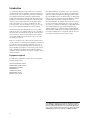
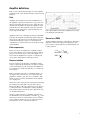
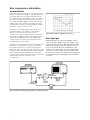
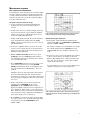
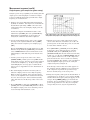
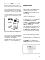
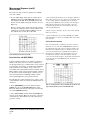
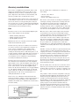
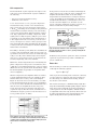
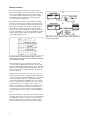
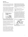
Agilent
Microwave Component Measurements
Amplifier Measurements Using the
Scalar Network Analyzer
Application Note 345-1
Introduction
A scalar network analyzer provides fast, economical
measurements of many amplifier parameters. This note
describes gain, gain compression, isolation, and return
loss (SWR) measurements using the Agilent 8757A
Scalar Network Analyzer and the Agilent 8350B Sweep
Oscillator to illustrate the techniques. Definitions and
specific step-by-step instructions are included, along
with a description of accuracy considerations. The
system features, such as alternate sweep, power sweep,
trace cursor and pass/fail limit lines are described.
All measurements described in this note are possible
without the use of a computer. However, it is possible to
automate these measurements using the same measurement sequences. For more information on the Agilent
8757A and amplifier measurements, refer to the references listed on page 15.
The Agilent 8757A is a powerful, easy to use scalar analyzer. It provides three detector inputs (a fourth input is
optional), and four independent display channels. With
the 11664A/E Detectors, the 8757A offers -60 dBm sensitivity at sweep speeds as fast as 50 ms. With the Agilent
85025A/B Detectors and the Agilent 85027A/B/C
Directional Bridges, the 8757A offers the choice between
two detection modes. In AC mode, the detectors detect
the envelope of signals modulated by a 27.778 kHz square
wave. This modulation is provided internally by the
Agilent 8350B sweep oscillator. Spurious unmodulated
signals and broadband noise are undetected. In DC detection mode modulation is not required, and the detector
responds to all signals in its frequency range.
This note describes how scalar network analysis can be
used to measure several important amplifier parameters
as a function of both frequency and input power. It is
important to keep in mind that many other factors can
affect amplifier performance, such as bias level, temperature, and time. In amplifier measurements, all these
variables must be taken into account for complete device
characterization.
Equipment required
The following equipment is used in the measurements
described in this note.
8757A Scalar Network Analyzer
8350B/83592A Sweep Oscillator*
85027B Directional Bridge
85025B Detectors
11667B Power Splitter
85023B Verification Kit
85022A system cable kit
* The 8350B Sweep Oscillator is used in all of the following measurement
setups. An 8340B or 8341B Synthesized Sweeper could also be used for applications requiring higher frequency accuracy and stability. When higher
source power is required to deliver more power to the device under test, the
8349B amplifier can be used to provide up to +18 dBm from 2-20 GHz.
2
Amplifier definitions
This section contains brief descriptions of the amplifier
parameters that can be measured using a scalar network
analyzer.
Gain
Amplifier gain is defined as the ratio (in milliwatts) of
the amplifier output power delivered to a ZO load to the
input power delivered from a ZO source, where ZO is the
characteristic impedance in which the amplifier is used
(50Ω in this note). In logarithmic terms, the gain is the
difference in dB, between the output and input power
levels, expressed in dBm.
Amplifier gain is most commonly specified as a minimum
gain value in the linear operating range. This would guarantee a given output power for a given input power. Since
variations in frequency response can cause distortion,
“gain flatness” is often specified over the frequency range
of the amplifier.
Gain compression
Figure 1−a shows an example plot of amplifier output
power versus input power at a single frequency. Gain at
any power level is the slope of this curve (Figure 1−b).
Notice that the amplifier has a region of constant gain,
where gain is independent of input power level.
Figure 1. Typical amplifier’s characteristics: (a) Output power versus input
power and (b) gain versus input power.
Return loss (SWR)
Another amplifier parameter commonly specified is the
impedance match at the input and output ports. The
most common scalar parameters are defined by the following equations:
ρ = Vreflected / Vincident
Return loss = −20 log10 ρ
SWR = 1+ρ
1−ρ
Reverse isolation
Reverse isolation is the measure of transmission from
output to input. The measurement of isolation is similar
to the measurement of gain, except that the amplifier is
reversed. Reverse isolation is typically 1.5 to 2 times the
forward gain.
This is commonly referred to as “small signal gain”. As
the input power is increased to a level that causes the
amplifier to saturate, gain decreases, causing the “large
signal” response, showing the limitation in the amplifier’s output power.
In this note, gain compression is measured by measuring
the output power when gain is decreased by 1 dB (see
Figure 1-b). This “1-dB gain compression point” (P1dB) is
a common measure of an amplifier’s output capability.
Both single frequency and swept gain compression tests
are described in this note.
Another common measure of amplifier output is Psat,
the maximum power an amplifier can deliver. Psat is the
output power level for which further increase in input
power yields no further increase in output power. Psat
measurements are not described in this note.
3
Gain, compression, and isolation
measurements
Gain, gain compression, and power can all be measured
using the setup shown in Figure 3. Note that ratioing is
performed using the power splitter. This ratioing improves the effective source match to remove the effects
of re-reflected signals and permits gain measurements
to be made at different RF power levels without recalibrating. Since source power level variations are monitored in both the reference and measurement channels,
their effect is removed from the ratio.
This same source match improvement can also be accomplished using source leveling, as described in
Ratioing or Leveling in the section Accuracy
Considerations. Also note that ratioing or source leveling could be accomplished using a directional coupler
such as the 11692D instead of a power splitter. The
coupler causes less power loss, but typically is not as
broadband as the power splitter.
Attenuation of the amplifier output is recommended as
required to keep the power level to the detectors in
their square law region of operation, below approximately −15 dBm, especially when gain compression will
be measured. Note that the attenuators will be included
in the transmission thru normalization, so their frequency response will be removed from the measurement
is described more in the section Accuracy
Considerations.
Figure 4. Example 8757A plot of amplifier gain vs. frequency
Small signal gain
Small signal gain is the gain in the amplifier’s linear
region of operation. Figure 4 shows an example swept
frequency gain measurement. Ratioing in this measurement removes frequency response and improves the effective source match. However, normalization is also
required, even when ratioing, to remove tracking differences between the two arms of the power splitter and
between the two detectors (B and R). This normalization
is also described in the small signal gain measurement
procedure.
Figure 3. Test setup for measuring amplifier gain and gain compression characteristics.
4
Measurement sequence
Small signal gain measurement
The following procedure describes the measurement of
small signal gain versus frequency.
1. Connect the instruments as shown in Figure 3.
Connect the B detector directly to the test port. (Do not
connect the device under test yet.)
2. Press [PRESET]* on the 8757A. This brings the analyzer and sweeper to a knon state.
3. Press the [CHAN 1 OFF] soft key on the 8757A. This
turns channel off, and leaves channel 2 being displayed
as the active channel.
4. Press [MEAS], then select [B/R]. This displays the
ratio B/R on channel 2.
5. Press [SYSTEM], then select the desired detection
mode, AC or DC. DC mode can be only used with the
85025 and 85026 series detectors. For a description of
these detection modes, refer to the section AC versus DC
Detection in Amplifier Measurements.
If using AC mode, skip step 6 and go to step 7.
6. Zero the DC detectors. To do this, press [CAL], then
select [DC DET ZERO]. Press [AUTOZRO]. This detector
zeroing should be repeated once every 5−10 minutes
when using DC mode. To do this automatically, turn on
[REPT AZ] in the DC DET ZERO menu, and set the
REPT AZ TIMER to the desired time value.
7. Set the desired START and STOP frequencies on the
source. Also set the source power level, keeping in mind
that you will have about 6 dB loss through the power splitter. To measure power at the test port, press
[CHANNEL 1], then [MEAS], then select [B]. Press
[SCALE], then select [AUTOSCALE] to view the data.
Press [CURSOR] and use the knob for a reading of
power and frequency across the trace. Adjust the power
level of the source to the desired level. Press
[CHANNEL 1], then press [CHAN 1 OFF] to turn
channel 1 off again.
8. Calibrate with the THRU connection. Press [CAL],
and select [THRU]. Be sure the THRU connection is
made, then press [STORE THRU] to place the calibration data into memory. Press [DISPLAY], then select
[MEAS-MEM] to view the normalized trace (B/R−M).
Sometimes averaging may be required during calibration
to remove the effects of noise. This becomes particularly
important when the detectors are measuring low level
signals (<−40 dBm). To activate averaging during calibration, select [AVG ON] in the thru calibration menu.
(The default averaging factor is 8). Wait until the trace
stabilizes before selecting [STORE THRU].
9. Insert the amplifier under test and apply the appropriate bias. (If averaging is on, restart averaging by
pressing [AVG], then [RESTART AVG].) Press [SCALE],
then [AUTOSCALE] to view then small signal gain. Press
[CURSOR], and use the knob for a reading of gain at
any point along the trace.
10. To measure gain variation or “ripple” in this frequency range, use the cursor delta function. Press
[CURSOR], select [MAX], then turn CURSOR D ON.
Now select [MIN]. The active entry area now displays
the total peak-to-peak variation in gain across the band
(see Figure 4)
*In this note, the Agilent 8757A front panel keys such as [PRESET] appear in
bold type, as opposed to the “softkeys” labeled on the CRT, which appear in
regular type (e.g. [CHAN 1 OFF])
5
Gain compression
Reverse isolation
There are several ways to measure amplifier gain compression using a scalar network analysis system. The
methods described here show how to cause 1−dB compression of the amplifier, then how to measure P1dB, the
amplifier output power when 1−dB compression occurs.
Both swept frequency and single frequency methods are
described. The first method is a swept frequency measurement, which uses Alternate Sweep mode to measure
small signal gain and large signal gain simultaneously.
Transmission from output to input is defined as the
reverse isolation of an amplifier. It can be measured
using the setup shown in Figure 8. Note that Figure 5 is
very similar to Figure 3 used to measure small signal
gain. The differences are that the amplifier is reversed,
and that the test port power level should be significantly
higher, as close as possible to the amplifier’s typical
output power level.
Swept gain compression
Swept gain compression measurements can be made
using the Alternate Sweep feature of the 8757 and the
8350 to alternate between two instrument states at different power levels (see Figure 6). Both small signal gain
and large signal gain can be viewed in real time. The difference between traces is due to compression. The
source power can be adjusted so that 1−dB compression
occurs at any desired frequency, and then the power out,
PldB, can be measured with a separate channel.
To measure isolation with the 8757A, follow the instructions for measuring small signal gain, making adjustments as needed.
Notice in this measurement that both traces are active,
so it is possible to see how device tuning affects both
small and large signal gain. This makes device tuning
more effective.
Normalized swept gain compression
In the alternate sweep measurement, it is difficult to see
exactly at which frequency 1−dB gain compression first
occurs. This can be more easily seen using normalization
to the small signal gain. Small signal gain is placed into
memory, then normalized. As the power level is increased,
compression can be observed as the drop from a flat reference line. The worst case frequency can be easily determined (see Figure 7). Notice that in this measurement,
the actual values of small and large signal gain are not
displayed.
Single frequency gain compression
The normalized compression measurement is a very
useful test for finding the worst case compression point.
Again, it is a swept frequency measurement of gain compression. Notice, however, that neither of the above
methods provides a systematic method of measuring the
power at 1 dB compression for a given frequency. This
can be accomplished using the power sweep feature of
the 8350B. At a single CW frequency, a power ramp is
input to the amplifier under test, and gain is measured
directly as a function of input power (see Figure 8).
Again, output power, P1dB can be displayed on a separate channel.
When using power sweep with the 8350B with RF plug-in
and the optional step attenuator, it is important to understand the interaction between the Automatic Leveling
Circuit (ALC) and the attenuator. For details on how to
sweep over a given range of power, see Appendix 2.
6
Figure 5. Test setup for measuring amplifier isolation.
Measurement sequence
Gain compression measurements
he following procedure describes how to measure amplifier gain compression. This measurement assumes that
you have already measured the small signal gain as described in the previous section. The setup and calibration data remain the same.
Swept gain compression (alternate sweep)
1. Be sure channel 2 is measuring normalized gain
(B/R−M). Note the power level indicated by the
sweeper.
2. Compression can be seen easily by simply increasing
the power level from the source. When the amplifier
saturates, the gain trace will fall. Return the power
level to the small-signal input level.
Figure 7. Example normalized swept frequency gain compression measurement. Gain compression is measured relative to small signal gain.
3. Display small signal gain (B/R−M) on both channels 1
and 2. Normalize both channels using the [CAL],
[THRU] sequence described in step 8 of the section on
gain measurements.
Normalized swept gain compression
1. With channel 1 still measuring normalized small
signal gain (B/RM), press [CHANNEL 1], [DISPLAY],
then select [MEAS−>MEM].
4. Connect the amplifier under test. Set the scale and
reference level to identical levels on both channels so
that the traces overlap. Both traces should show the
amplifier’s small signal gain.
The channel 1 display is now normalized to the ampli
fier’s small signal gain. Press [SCALE] and select
[AUTOSCALE]. The trace should be a flat line near
0 dB.
5. Enable ALTERNATE SWEEP. On the source, press
[SAVE] [1], then press [ALT n] [1]. The system is
now alternating between two identical states, and the
traces should still overlap.
2. Increase the source power level until the trace falls by
1−dB at some frequency. An example is shown in
Figure 7. This display shows compression from a flat
trace, but does not show the actual values of small
signal or large signal gain.
6. Press [CHANNEL 1], then increase the source power
level on the present state by pressing [POWER
LEVEL] and turning the knob. As the amplifier satu
rates, the channel 1 trace will fall Figure 6 shows an
example.
Note again that power out (or in) can be displayed on
channel 3. Read power at 1−dB compression.
Channel 1 shows the large signal gain, and channel 2
shows the small signal gain. The system alternates
between the two input power levels. Gain compression
at any frequency is simply the differ-ence between the
two traces.
7. In this configuration, power can be measured on
channel 3. Press [CHANNEL 1], then select
[CHANNEL 3]. Press [MEAS] and select [B] to
display the amplifier output power in compression or
[R] to display the input power to cause compression.
Since channels 1 and 3 are alternated with channels 2
and 4, channel 3 in this configuration will display the
large signal output power (see Figure 6).
Figure 6. Example swept frequency gain compression measurement using
the Alternate Sweep mode. The large signal gain trace shows amplifier gain
compression.
8. Press [ALT n] to deactivate alternate sweep. Return
the source power level to the small signal input. Turn
off channel 2 by pressing [CHANNEL 2], then
[CHAN 2 OFF].
7
Measurement sequence (cont’d)
Single frequency gain compression (power sweep)
Using the power sweep capability of the 8350B, gain and
output power can be displayed as a function of input
power level. This measure-ment, performed at a single
frequency, is described below.
1. Return to the swept small signal gain measurement
(B/R−M) on channel 1. You may need to normalize the
measurement again using a THRU connection as de
scribed in the first section. Display output power (B)
on channel 3.
Activate the adaptive normalization feature of the
8757A. Press [SYSTEM], then select [ADPT NM ON].
With adaptive normalization, as the frequency is
changed, the calibration data will be adjusted.
2. Set any desired CW frequency on the source within
the range of the original calibration. Press [SHIFT]
[CW], then enter the frequency, for example [1] [0]
[GHz].
The left hand LED display should display zeroes. This
indicates swept CW mode ([SHIFT CW]), in which the
source SWEEP OUT drives the horizontal axis of the
8757A display to make this axis power instead of frequency.
3. Activate power sweep mode on the source. Press
[POWER SWEEP], and the power sweep LED should
be lit. On the sweeper, enter the sweep range required
to saturate the amplifier, e.g. 10 dB per sweep. Most
8350B RF plug-ins can sweep up to 15 dB from the
start power. See Appendix 2 for more information on
using the
4. The 8757A display should now show the gain as a
function of input power level at a single frequency.
Figure 8 shows an example. Notice that the gain decreases as the amplifier enters saturation. If the gain
does not decrease by the desired amount (usually
1 dB), then increase the dB/sweep value or the start
power.
5. Press [CHANNEL 1], then select [CHANNEL 3]. Press
[SCALE], then select [AUTOSCALE]. This trace shows
the amplifier output power. Notice that this power in
creases linearly until saturation occurs.
8
Figure 8. Single frequency gain compression measurement using the Power
Sweep feature. Gain (and power) are displayed as a function of input power.
6. Find the power out at 1−dB compression. Use the
cursor search function on channel 1, the 1−dB compression point can be found. The power out can then
be read off the channel 3 cursor.
Press [CHANNEL 1], [CURSOR], and select [MAX].
Activate the cursor delta function by selecting
[CURSOR D ON]. Press [SEARCH], then select
[SEARCH VALUE] and enter the desired search value,
in this case –1.0 dB. Select [SEARCH RIGHT] and the
cursor symbol will move to the 1−dB compression
point. Deactivate the cursor search trace hold by
pressing [CURSOR]. The channel 3 cursor should now
read the amplifier output power at the 1−dB gain
compression point (see Figure 8).
If the message “Cursor value not found” appears on
the analyzer, then the amplifier is not reaching its
1−dB compression point in the specified sweep.
Increase the dB/Sweep or the start power.
7. Change the frequency and repeat the measurement. A
convenient way to do this is to set a step size in GHz,
and increment the frequency using the [↑] key on the
sweeper. Press [SHIFT] [CW] [↑] to increment the
frequency. It is not normally necessary to adjust the
power sweep parameters once they are set up. The
sweeper must, however, stay in swept CW mode.
Return loss/SWR measurements
Return loss and SWR are commonly specified for the
amplifier input and output ports. With the 8757A, reflection can be displayed as return loss in dB or in standing
wave ratio (SWR).
Measurement Sequence
The reflection measurement setup shown in Figure 9
could be used for simultaneous reflection and transmission measurements. The 8757A can be easily configured
to display return loss on channel 1 and gain on channel
2. If the reflection measurement is made with a separate
setup, ratioing may not be required, since the measurement is often only made at one power level. If reflection
is tested at several power levels, then ratioing is recommended.
1. Connect the equipment as shown in Figure 9. Ratioing
with the power splitter may not be required.
The following procedure describes basic reflection
measurements with the 8757A.
2. Activate channel 1 and turn all other channels off.
Press [MEAS] and select [A/R]. Channel 1 will then
display input A/R.
3. Press [SYSTEM], and select the desired detection
mode AC or DC. Either detection can be used with any
of the 85027 series directional bridges.
If using AC detection mode, skip step 4 and go to step 5.
4. Zero the DC accessories. To do this, press [CAL], then
select [DC DET ZERO]. Press [AUTO ZERO].
This detector zeroing should be repeated once every
5−10 minutes. To do this automatically, turn on [REPT
AZ] in the DC DET ZERO menu, and set the REPT AZ
TIMER to the desired time value.
5. Set the desired START and STOP frequencies on the
source. Also set the source power level. Remember, you
will have approximately 6−8 dB loss through the direc
tional bridge.
Figure 9. Test setup for simultaneous measurement of amplifier gain and
input return loss.
Reflection parameters can be measured with a directional bridge or with a directional coupler and another detector. The setup of Figure 9 describes the measurement
with an 85027B Directional Bridge, but also applies to a
directional coupler, such as the 11692D.
Calibration for reflection measurements is performed by
normalizing to the average response of a short circuit
and an open circuit. This removes errors that occur
during calibration, due to directivity and source match.
This is discussed further in Accuracy Considerations.
6. Press [CAL] and select [SHORT/OPEN]. This initiates
the short/open calibration procedure. As prompted,
connect the short circuit and press [STORE SHORT].
Again as prompted, connect the shielded open circuit
and press [STORE OPEN].
This procedure places the short/open average into the
channel 1 memory. Press [DISPLAY], then select
[MEAS-MEM] to normalize the display trace.
7. Connect the device under test. Connect in the forward
direction to measure input return loss or in the reverse
direction for output return loss.
8. Press [SCALE] and select [AUTOSCALE]. Press
[CURSOR] and use the knob to read the return loss in
dB at any point along the trace. Figure 10 shows an
example.
Figure 11. Example input SWR plot in dB.
9
Measurement Sequence (cont’d)
Measuring SWR
The reflection data can also be displayed as standing
wave ratio (SWR).*
9. To view SWR, simply change the trace format. Press
[DISPLAY], then select [TRC FMT SWR]. The trace is
then displayed in SWR. Press [CURSOR] and use the
knob to view the SWR at any point along the trace (see
Figure 11).
The trace format can be changed at any time without
affecting the calibration in trace memory. Even if the
calibration is performed while in SWR trace mode,
the calibration (stored in dB) is still valid.
3. The analyzer will prompt you for the upper and lower
limit values. In this case, we only use a lower limit, since
we are testing against a minimum gain specification.
Just press the [ENT] key when prompted for the upper
limit. When prompted for the lower limit, enter the
minimum gain specification and terminate the entry
with the [dB/dBm] key.
4. Repeat steps 1 through 3 above as necessary until all
limits are entered.
5. Turn on limit lines by selecting [DONE], then [LIM
LNS ON]. Figure 12 shows an example limit entry with 3
flat segments.
Saving the measurement
Figure 10. Example input return loss plot in dB.
Using limit lines and SAVE/RECALL
Using the limit line feature of the 8757A, specification
limits can be entered on the screen for comparison to
the measured data. Up to 12 limit entries can be entered
as point limits, sloped lines, or flat lines. The minimum
gain specification, for example, can be entered as a
lower limit. If the gain falls below this lower limit, then a
FAIL condition exists. Upper and lower limits could also
be entered for testing of gain ripple or flatness. For reflection measurements, a SWR upper limit could be
entered and displayed as the pass/fail criterion.
Once a measurement is configured, it can be stored for
future use in one of the nine SAVE/RECALL registers of
the 8757A. The first four of these registers will also save
limit lines and calibration data for channels 1 and 2. To
store a measurement, press [SAVE], then a number 1
through 9. No terminator is required. This saves your
measurement settings of both the analyzer and the
source in non-volatile memory. Recall that measurement
at any time by pressing [RECALL] and entering the
same number.
The following procedure describes how to enter a series
of flat limit line entries for testing the minimum gain on
channel 2.
1. Press [CHANNEL 2] to activate channel 2. Press
[SPCL], then press the [ENTER LMT LNS] soft key.
Erase any limits that may have already been entered by
selecting [DELETE ALL LNS].
2. Select [FLAT LIMIT], and the label “FLAT FREQ #1?”
appears on the display. Enter the frequency of the start
of the limit line, and terminate the entry using the appropriate soft key.
* To display SWR, the 8757A requires firmware revision 2.0 or higher. If your
8757A has revision less than 2.0, order the 11614A Firmware Enhancement to
upgrade.
10
Figure 12. (a) Example limit line entries for minimum gain specification and
(b) plot showing limit lines, gain trace and PASS/FAIL status.
Accuracy considerations
The accuracy of amplifier measurements with a scalar
analyzer is determined by many factors. This section
summarizes the key accuracy considerations for gain,
gain compression, and return loss measurements, and
discusses possible ways of reducing these errors.
Some applications may require better accuracy than the
scalar analyzer can provide. A vector network analyzer,
such as the 8510A, not only provides phase data, but
also provides vector accuracy enhancement and immunity to harmonics and other spurious signals. The result is
significantly better measurement accuracy.
Gain
The major sources of error in measuring amplifier gain
with a scalar analyzer are the following:
• mismatch during calibration
• mismatch during measurement
• system dynamic accuracy
Mismatched errors are caused by re-reflection signals
within the measurement system.
Mismatch during calibration results because the detector reflects a portion of the signal back toward the “effective source” (actually the power splitter). This
reflected signal is then re-reflected from the source,
causing an uncertainty which could add in phase or out
of phase with the original signal. With detector match of
16 dB and effective source match of 20 dB, the worst
case mismatch error in calibration is approximately
±0.14 dB (from mismatch calculator).
Mismatch during measurement is caused by two separate mismatches: the mismatch between the amplifier
input and the source, and the mismatch between the amplifier output and the detector. For example, with an effective source match of 20 dB and an amplifier input
match of 10 dB, the first mismatch error is approximately
±0.3 dB. With an amplifier output match of 10 dB and
detector match of 16 dB, the second mismatch error is
approximately ±0.4 dB. So the total mismatch error
during measurement is ±0.7 dB.
In the worst case, calibration and measurement mismatch uncertainties combine to form a larger window of
uncertainty, as shown in Figure 14. It is important to
minimize the mismatches to minimize the total measurement uncertainty.
The uncertainty due to mismatches is a function of
three things:
• effective source match
• detector match
• match of the amplifier under test.
The effective source match can be improved using three
techniques: ratioing, external source leveling, and isolation. Ratioing was used in the above example. For a
comparison of ratioing and leveling, see Ratioing or
Leveling. Isolation can be accomplished most easily with
an attenuator on the output of the source. This attenuation decreases the magnitude of the re-reflected signal.
Effective detector match can be improved by inserting
an attenuator before the detector. This improvement
would be significant only if the attenuator has far better
match than the detector. As the attenuation is increased, the “effective detector match” approaches the
match of the attenuator. Amplifier match is normally a
function of the amplifier design and cannot be further
im- proved. However, it is important to realize that
measurements of a well-matched amplifier will typically
contain less uncertainty than those of a poorly matched
amplifier.
Dynamic accuracy also influences gain measurement uncertainty. Gain is a relative measurement, that is, the
output power relative to the input power measured with
the thru normalization. This normalization accounts for
the frequency response of the detectors. However, the
system’s response is also a function of power level.
Specifically, if the power level seen by the detector is different between calibration and measurement, then the
detector response causes an additional uncertainty in
the measurement of gain.
The uncertainty due to the detector is a function of how
much the power changes between calibration and measurement. This is specified on systems as “dynamic accuracy.” Detector error over a 30 dB range is typically ±0.1
dB.
It is possible to reduce the effects of dynamic accuracy by
inserting attenuation during the measurement (after calibration) to keep the calibration power level as close as
possible to the measurement power level. For high gain
measurements (>30 dB), this “post-attenuation” or RF substitution technique is recommended. However, the frequency response of the external attenuator must be
removed from the measurement, since it is not included
during the calibration process. The 8757A detector offset
function can remove a nominal attenuation value from the
measured data.
Figure 14. Total mismatch uncertainty includes both calibration and measurement uncertainty as shown.
11
Gain compression
The measurement of gain compression is subject to the
same errors as the measurement of gain, in addition to
the following:
• detector power measurement accuracy
• harmonics at the detector
Power measurement accuracy. A gain compression
measurement really consists of two measurements,
first of gain, then of power when gain compresses by
1 dB (P1dB). Normally, the uncertainty in the gain measurement will not translate directly to the uncertainty
of the power measurement. When measuring compression, large signal gain is normally compared to small
signal gain at a single frequency. Only the power level
is changed. So the uncertainty in the measurement of
1−dB compression is the uncertainty in the measurement of the difference between small signal gain and
large signal gain. This will be determined by the dynamic
accuracy of the detectors and by how much the amplifier’s
match varies as it saturates.
The ability to measure power (dBm) also determines the
accuracy of the measurement of PldB. Power accuracy is
specified for the 85025 series detectors in DC mode (typically ± 0.15 dB), and is enhanced by referencing the
detector to a power meter sensor as described in the
85025A/B Operating and Service Manual.
If the power level at the detector must remain high, filtering can be used to reduce the effect of harmonics on
amplifier measurements. This can be done using a
lowpass filter for measurements covering less than one
octave. An example is shown in Figure 16−a. For more
broadband measurements, a tracking filter can be connected as shown in Figure 16−b. In either case the
effects of the filter (mismatch, frequency response, etc.)
must be included in any uncertainty analysis.
Figure 16. The effects of harmonics can be reduced using (a) a low pass
filter when measuring less than one octave or (b) using a tracking filter for
broadband measurements.
If filtering is not practical, operate the detectors in their
square law region whenever possible to minimize the
effects of harmonics.
Harmonics. Another important factor in measuring amplifier compression is the presence of harmonics, most
commonly second and third harmonics of the test signal.
(Harmonics are also present in the measurement of gain,
but their magnitude is typically low enough that their
effect is negligible.)
Return loss
When in compression, the amplifier under test tends to
generate higher harmonic levels (for example 20 dBc),
and this affects the accuracy of the scalar analyzer.
Figure 15 shows the worst case uncertainty of a scalar
power measurement in the presence of second harmonics, 15, 20, 25, and 30 dB below the fundamental. Notice
that the errors are insignificant at the lower power
levels, where the detector measures total rms power
(square law region). For this reason, attenuation is recommended to keep the power level at the B detector as
low as possible (below −15 dBm).
where ∆ρ is the uncertainty in the reflection coefficient,
ρL is the reflection coefficient of the device under test,
A is directivity, B is calibration uncertainty, and C is
the effective source match.
Figure 15. Worst case deviation from ideal square law operation, due to
second harmonics when using a scalar network analyzer. Notice that the uncertainty is greater for high harmonic levels and at the higher power levels
when the detector is in its linear operating region.
12
The uncertainty of return loss measurements is described by the following equation:
∆ρ = A = BρL + CρL2
The A term can be kept to a minimum using a high directivity directional bridge and high quality adapters. The B
term can be removed through open/short averaging if a
coaxial system is used. In waveguide, calibration can be
accomplished with a short only (B=A+C). The C term can
be reduced by improving source match using the techniques already discussed for gain measurements.
Ratioing or leveling
In a swept frequency measurement, effective source
match can be improved either by ratioing or by leveling
the source externally. Both methods provide similar
source match improvement. However, there are important distinctions between the two techniques. This
section describes the differences.
Ratioing improves effective source match by reducing
the effect of source power variations versus frequency.
Because the power variations appear in both detectors
(B and R, for example), they are not seen in the ratio
(B/R). Figure 17 shows a typical plot of B,R, and the
ratio B/R. Notice that while B/R is relatively flat, B can
vary by approximately ±0.5 dB. Some amplifier measurements can be adversely affected by this type of ripple,
particularly with fast sweeps.
Figure 18. Source leveling techniques (a) using an external crystal detector
and (b) using a power meter.
Figure 17. Comparison of leveling and ratioing techniques. Frequency response at the test port, using (a) internal source leveling, (b) the ratio B/R,
and (c) external source leveling.
When ratioing, the power variation at the test port
occurs because of mismatch between the detector and
the source during calibration, and between the amplifier
and the source during measurement. In either case, the
R detector tracks the variations and they are removed
from the ratio B/R.
While ratioing removes the effect of the source power
variations, external source leveling actually reduces the
variations directly. As shown in Figure 18−a, an external
detector provides feedback to an automatic leveling
circuit (ALC) which then modulates the source output
power to compensate for mismatch at the test port. The
result is that the source output power is flatter as a
function of frequency (see Figure 17). For further information on external source leveling see Product Note
8350−9. The source power can also be leveled using the
recorder output of a power meter, as shown in Figure
18−b.
The major advantage of external or power meter source
leveling is that the power at the test port is controlled by
a feedback loop, and is not subject to variations due to
mismatch at the test port. However, ratioing is often
more convenient and easy to use than source leveling.
13
Appendix 1
AC versus DC detection
The 8757A offers a choice of detection modes: AC detection, which uses modulation for immunity to broadband
noise and thermal drift, and DC detection, which offers
fast accurate power measurements without modulation.
This section describes the capabilities and advantages of
each mode when measuring amplifiers.
In AC mode, the RF source is modulated by a 27.778 kHz
square wave. The detector then processes only the modulated signal (see Figure A−1). (The 8350B sweep oscillator provides this modulation internally). Other signals,
such as DC or thermal drift, broadband noise, and spurious signals from other sources are unmodulated and
therefore go undetected. AC detection is ideal for most
relative measurements, such as gain and return loss, particularly in the presence of undesired, unmodulated
signals. AC detection also requires no detector zeroing.
AC mode is the better choice whenever the low levels
signals must be detected in the presence of higher level
broadband noise. Figure B shows an output return loss
measurement where the signal returned from the amplifier
is actually at a lower level than the amplifier’s broadband
noise floor. AC detection rejects the noise and detects the
return signal. With DC detection, the noise masks the
return signal.
Some amplifiers can be affected by the 27.778 kHz modulation. Some examples are the following
• Amplifiers with Automatic Gain Control (AGC)
• Amplifiers with high gain at very low frequencies
(<l MHz)
• Amplifiers with slow responding self bias
The measurement of an amplifier with AGC is shown in
Figure C. Note that the function of an AGC is to provide
a desired output power over a whole range of input
power levels. Figure C shows the measurement made in
both AC and DC detection modes. In DC mode, the amplifier input and output are unmodulated. The detector
downconverts to a DC level, then chops the signal to
form a 27.778 kHz square wave for the receiver. The
same measurement in AC mode (RF modulated) shows
that the leveling circuit is adversely affected by the modulation. The AGC tries to adjust its gain to track the
modulation, but cannot. The resulting square wave is
distorted and the scalar analyzer response is degraded.
Note that DC detection is the better choice in this application.
Figure A. Comparison of detection modes. (1) AC detection uses RF modulation, (2) DC detection detects unmodulated RF, then chops the detected
signal. The receiver sees the same type square wave signal in either mode.
In DC mode, the detectors respond to all signals present,
and 27.778 kHz source modulation is not required. As
shown in Figure A−2, when in DC mode, the 85025 series
Detectors chop the signal after detection to provide a
27.778 kHz square wave to the receiver. The receiver circuitry used is identical in both modes.
The choice between detection modes depends on the particular application. In many applications, the choice is
arbitrary, because the results in either mode would be identical. But some applications are more suited to one
mode or the other.
Figure B. AC detection rejects unwanted signals that are unmodulated, such
as the RF noise at the amplifier output.
Absolute measurements of power (dBm) are usually
more accurate in DC detection mode, because the measurement is not subject to variations in source modulation. DC mode is usually a better choice for measuring
power out at 1 dB gain compression, for example. In AC
mode, power measurements are subject to changes in
and square wave duty cycle. In addition, DC mode is
more easily referenced to a power meter. In AC mode
since the source is square wave modulated, the power
meter reading would be nominally 3 dB lower than the
scalar analyzer reading. This is not the case in DC mode.
14
Appendix 1 (cont’d)
Appendix 2
AC versus DC detection
8350B powersweep
If there is any doubt about which detection mode is the
better choice in a particular measurement, try both
methods and compare the results. The 85025 series detectors can operate in either mode. If there is no significant difference, then the choice may be arbitrary. If
there is a difference, evaluate which method is more accurate and make all measurements in that mode.
All 83500 series RF plug-ins have a power sweep capability that utilizes the internal ALC circuitry of the plug-in to
ramp the power out. The ALC dynamic range is determined by the minimum settable power and the maximum
leveled output power of the plug-in.
Figure C. Example measurement of amplifier with automatic gain control
(AGC) (1) measurement setup and (2) measured gain in AC and DC detection modes. DC detection is better in this application.
If the plug-in has the optional step attenuator installed
(Option 002), then the maximum leveled output power
(and therefore, the dynamic range) will decrease due to
the insertion loss of the internal attenuator. In addition,
this attenuator cannot be switched during a power sweep
due to the excessive wear that would be inflicted on the
attenuator switches. In normal operation the ALC and attenuator are coupled and the values are automatically set
when the power level is entered. However, the two can be
decoupled and controlled independently by pressing
[SHIFT][SLOPE] to set the attenuator value and
[SHIFT][POWER LEVEL] to set the ALC power level.
Decoupling the ALC from the attenuator potentially
allows you to use the full range of the ALC circuitry.
Changing just the attenuator value (internal and/or external) will not change the ALC level. Changing just the ALC
power level will change both the output power level and
the ALC range of operation.
Let’s look at an example using the 8350B with the 89592A
RF plug-in. The ALC dynamic range of this plug-in is −5
dBm to +10 dBm, allowing 15 dB of power sweep range.
Assume that we want to sweep power from −21 dBm to −6
dBm. On the 83592A plug-in, press [POWER LEVEL] and
enter −21 dBm. 20 dB of attenuation is automatically
switched in and the low end of the ALC range is set to −1
dBm. Press [POWER SWEEP] and enter 15 dB/sweep.
The power is now being swept from −21 dBm to −6 dBm,
and the ALC is operating from −1 dBm to + 14 dBm. This
is not within the allowable −5 dBm to +10 dBm ALC range
of the plug-in. To remedy this, decouple the ALC from the
attenuator and add a 6 dB external attenuator. Press
[SHIFT] [SLOPE] and enter 10 dB of attenuation. This,
plus the 6 dB of external attenuation, provides 16 dB of
attenuation for the system. Press [SHIFT] [POWER
SWEEP] and enter −5 dBm. The plug-in now operates over
the full −5 dBm to + 10 dBm ALC dynamic range.
The same method can be applied to the 8340B or 8341B.
The internal step attenuator is standard on both instruments. [SHIFT] [POWER SWEEP] decouples the ALC from
the attenuator. “ATTN: -XX dB, ALC: X.XX dBm” appears
in the ENTRY DISPLAY. The ALC power level is set with
the keypad or knob and the attenuator is set with the step
keys. The performance of the synthesized sweeper is optimized when the ALC operates within the range of -20
dBm to +20 dBm. As an example, assume that the 8340B
or 8341B has a maximum leveled output power of +10
dBm. This means that the ALC can operate from -20 dBm
to +10 dBm (as opposed to −5 dBm to +10 dBm for the
8350B). The synthesized sweeper has 15 dB more dynamic
range available as compared to the 8350B. A minimum
power sweep range of 20 dB can be achieved in any part
of the dynamic range without using any external attenuation.
15
Application Note 326, “Principals of Microwave Connector Care,”
literature no. 5954-1566.
Agilent Technologies’ Test and Measurement Support, Services,
and Assistance
Agilent Technologies aims to maximize the value you receive, while minimizing your risk and problems. We strive to ensure that you get the test
and measurement capabilities you paid for and obtain the support you
need. Our extensive support resources and services can help you
choose the right Agilent products for your applications and apply them
successfully. Every instrument and system we sell has a global warranty. Support is available for at least five years beyond the production life
of the product. Two concepts underlie Agilent's overall support policy:
"Our Promise" and "Your Advantage."
“Barretter and Diode Comparison For Insertion-Loss
Measurements in the Presence of Harmonics,” by Fritz K.
Weinert, Dr. Bruno 0. Weinschel, and Donald D. Woodruff,
Microwave journal, March, 1975, pp. 39-43.
Product Note 8350A-6, “Reduced Harmonic Distortion Using the
Integra TMF-1800H Tracking Filter with the 8350 Sweep
Oscillator,” literature no. 5952-9345. Integra Microwave, Santa
Clara, California.
Our Promise
Our Promise means your Agilent test and measurement equipment will
meet its advertised performance and functionality. When you are choosing new equipment, we will help you with product information, including
realistic performance specifications and practical recommendations
from experienced test engineers. When you use Agilent equipment, we
can verify that it works properly, help with product operation, and provide
basic measurement assistance for the use of specified capabilities, at
no extra cost upon request. Many self-help tools are available.
Application Note FT2, “Ferretrac Hands-Off Tracking Filter
Reduces Spurious and Harmonic Output Signals from RF
Sources.” Ferretec, Inc., San Jose, California.
Your Advantage
Your Advantage means that Agilent offers a wide range of additional
expert test and measurement services, which you can purchase according to your unique technical and business needs. Solve problems efficiently and gain a competitive edge by contracting with us for
calibration, extra-cost upgrades, out-of-warranty repairs, and on-site
education and training, as well as design, system integration, project
management, and other professional engineering services.
Experienced Agilent engineers and technicians worldwide can help you
maximize your productivity, optimize the return on investment of your
Agilent instruments and systems, and obtain dependable measurement accuracy for the life of those products.
List of references
Application Note 183, “High Frequency Swept Measurements,”
literature no. 5952-9200.
Application Note 329, “Performance Characteristics of
Microwave Signal Sources,” literature no. 5953-8883.
8757A Scalar Network Analyzer Operating Manual, part no.
08757-90034.
8350B Sweep Oscillator Operating and Service Manual, part no.
08350-90034.
Product Note 8350-9, “Improving the output power flatness of the
8350B Sweep Oscillator,” literature no. 5954-8344.
By internet, phone, or fax, get assistance with all your test and measurement needs.
Online assistance:
www.agilent.com/find/assist
Phone or Fax
United States:
(tel) 1 800 452 4844
Canada:
(tel) 1 877 894 4414
(fax) (905) 282-6495
Europe:
(tel) (31 20) 547 2323
(fax) (31 20) 547 2390
Japan:
(tel) (81) 426 56 7832
(fax) (81) 426 56 7840
Latin America:
(tel) (305) 269 7500
(fax) (305) 269 7599
Australia:
(tel) 1 800 629 485
(fax) (61 3) 9210 5947
New Zealand:
(tel) 0 800 738 378
(fax) 64 4 495 8950
Asia Pacific:
(tel) (852) 3197 7777
(fax) (852) 2506 9284
Product specifications and descriptions in this document subject to
change without notice.
Copyright © 2001 Agilent Technologies
Printed in USA May 15, 2001
5954-1599