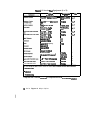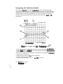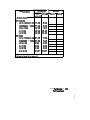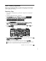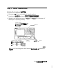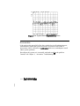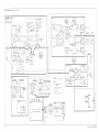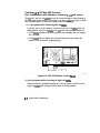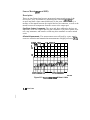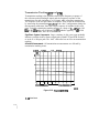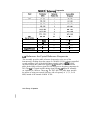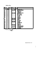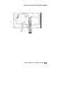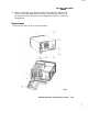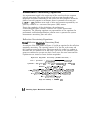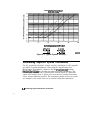
1
Service Guide Agilent Technologies 8719D/20D/22D Network Analyzers Manufacturing Part Number: 08720-90292 Printed in USA Print Date: February 1999 Supersedes: June 1998 © Agilent Technologies, Inc. 1996 - 1999 Hewlett-Packard to Agilent Technologies Transition This manual may contain references to HP or Hewlett-Packard. Please note that Hewlett-Packard's former test and measurement, semiconductor products and chemical analysis businesses are now part of Agilent Technologies. To reduce potential confusion, the only change to product numbers and names has been in the company name prefix: where a product number/name was HP XXXX the current name/number is now Agilent XXXX. For example, model number HP 8720D is now model number Agilent 8720D. Documentation Warranty THE MATERIAL CONTAINED IN THIS DOCUMENT IS PROVIDED "AS IS," AND IS SUBJECT TO BEING CHANGED, WITHOUT NOTICE, IN FUTURE EDITIONS. FURTHER, TO THE MAXIMUM EXTENT PERMITTED BY APPLICABLE LAW, AGILENT DISCLAIMS ALL WARRANTIES, EITHER EXPRESS OR IMPLIED WITH REGARD TO THIS MANUAL AND ANY INFORMATION CONTAINED HEREIN, INCLUDING BUT NOT LIMITED TO THE IMPLIED WARRANTIES OF MERCHANTABILITY AND FITNESS FOR A PARTICULAR PURPOSE. AGILENT SHALL NOT BE LIABLE FOR ERRORS OR FOR INCIDENTAL OR CONSEQUENTIAL DAMAGES IN CONNECTION WITH THE FURNISHING, USE, OR PERFORMANCE OF THIS DOCUMENT OR ANY INFORMATION CONTAINED HEREIN. SHOULD AGILENT AND THE USER HAVE A SEPARATE WRITTEN AGREEMENT WITH WARRANTY TERMS COVERING THE MATERIAL IN THIS DOCUMENT THAT CONFLICT WITH THESE TERMS, THE WARRANTY TERMS IN THE SEPARATE AGREEMENT WILL CONTROL. DFARS/Restricted Rights Notice If software is for use in the performance of a U.S. Government prime contract or subcontract, Software is delivered and licensed as “Commercial computer software” as defined in DFAR 252.227-7014 (June 1995), or as a “commercial item” as defined in FAR 2.101(a) or as “Restricted computer software” as defined in FAR 52.227-19 (June 1987) or any equivalent agency regulation or contract clause. Use, duplication or disclosure of Software is subject to Agilent Technologies’ standard commercial license terms, and non-DOD Departments and Agencies of the U.S. Government will receive no greater than Restricted Rights as defined in FAR 52.227-19(c)(1-2) (June 1987). U.S. Government users will receive no greater than Limited Rights as defined in FAR 52.227-14 (June 1987) or DFAR 252.227-7015 (b)(2) (November 1995), as applicable in any technical data. Printing Copies of Documentation from the Web To print copies of documentation from the Web, download the PDF file from the Agilent web site: • Go to http://www.agilent.com. • Enter the document’s part number (located on the title page) in the Quick Search box. • Click GO. • Click on the hyperlink for the document. • Click the printer icon located in the tool bar. Contacting Agilent This information supersedes all prior HP contact information. Online assistance: www.agilent.com/find/assist Americas Brazil (tel) (+55) 11 3351 7012 (fax) (+55) 11 3351 7024 Mexico (tel) 1 800 254 2440 (fax) 1 800 254 4222 Canada (tel) +1 877 894 4414 (fax) +1 303 662 3369 United States (tel) 800 829 4444 (alt) (+1) 303 662 3998 (fax) 800 829 4433 Asia Pacific and Japan Australia (tel) 1 800 225 574 (fax) 1 800 681 776 (fax) 1 800 225 539 China (tel) 800 810 0508 (alt) 800 810 0510 (fax) 800 810 0507 (fax) 800 810 0362 Hong Kong (tel) 800 933 229 (fax) 800 900 701 India (tel) 1600 112 626 (fax) 1600 112 727 (fax) 1600 113 040 Japan (Bench) (tel) 0120 32 0119 (alt) (+81) 426 56 7799 (fax) 0120 01 2144 Japan (On-Site) (tel) 0120 802 363 (alt) (+81) 426 56 7498 (fax) (+81) 426 60 8953 Singapore (tel) 1 800 275 0880 (fax) (+65) 6755 1235 (fax) (+65) 6755 1214 South Korea (tel) 080 778 0011 (fax) 080 778 0013 Taiwan (tel) 0800 047 669 (fax) 0800 047 667 (fax) 886 3492 0779 Thailand (tel) 1 800 2758 5822 (alt) (+66) 2267 5913 (fax) 1 800 656 336 Malaysia (tel) 1800 880 399 (fax) 1800 801 054 Europe Finland (tel) (+358) 10 855 2100 (fax) (+358) (0) 10 855 2923 Austria (tel) 0820 87 44 11* (fax) 0820 87 44 22 Belgium (tel) (+32) (0)2 404 9340 (alt) (+32) (0)2 404 9000 (fax) (+32) (0)2 404 9395 Denmark (tel) (+45) 7013 1515 (alt) (+45) 7013 7313 (fax) (+45) 7013 1555 France (tel) 0825 010 700* (alt) (+33) (0)1 6453 5623 (fax) 0825 010 701* Germany (tel) 01805 24 6333* (alt) 01805 24 6330* (fax) 01805 24 6336* Israel Ireland (tel) (+353) (0)1 890 924 204 (tel) (+972) 3 9288 500 (alt) (+353) (0)1 890 924 206 (fax) (+972) 3 9288 501 (fax)(+353) (0)1 890 924 024 Italy (tel) (+39) (0)2 9260 8484 (fax) (+39) (0)2 9544 1175 Luxemburg (tel) (+32) (0)2 404 9340 (alt) (+32) (0)2 404 9000 (fax) (+32) (0)2 404 9395 Netherlands (tel) (+31) (0)20 547 2111 (alt) (+31) (0)20 547 2000 (fax) (+31) (0)20 547 2190 Russia (tel) (+7) 095 797 3963 (alt) (+7) 095 797 3900 (fax) (+7) 095 797 3901 Spain (tel) (+34) 91 631 3300 (alt) (+34) 91 631 3000 (fax) (+34) 91 631 3301 Sweden (tel) 0200 88 22 55* (alt) (+46) (0)8 5064 8686 (fax) 020 120 2266* Switzerland (French) (tel) 0800 80 5353 opt. 2* (alt) (+33) (0)1 6453 5623 (fax) (+41) (0)22 567 5313 Switzerland (German) (tel) 0800 80 5353 opt. 1* (alt) (+49) (0)7031 464 6333 (fax) (+41) (0)1 272 7373 Switzerland (Italian) (tel) 0800 80 5353 opt. 3* (alt) (+39) (0)2 9260 8484 (fax) (+41) (0)22 567 5314 United Kingdom (tel) (+44) (0)7004 666666 (alt) (+44) (0)7004 123123 (fax) (+44) (0)7004 444555 (tel) = primary telephone number; (alt) = alternate telephone number; (fax) = FAX number; * = in country number 11/16/04 Service Guide i 8719D/2OD/22D Network Analyzer Ra HEWLETT PACKARD HP part number: 08720-90292 Supersedes June 1998 Printed in USA February 1999 Notice. The information contained in this document is subject to change without notice. Hewlett-Packard makes no warranty of any kind with regard to this material, including but not limited to, the implied warranties of merchantability and fltness for a particular purpose. Hewlett-Packard shall not be liable for errors contained herein or for incidental or consequential damages in connection with the fur&hing, performance, or use of this material. @Copyright 1996-1999 Hewlett-Packard Company Network Analyzer Documentation Set The Instalhtion and Quick Start Guide familiarizes you with the network analyzer’s front and rear panels, electrical and environmental operating requirementq as well as procedure8 for installing, conflghng and verifying the operation of the aualyze~ The UaeFs Gpide shows how to make measurementq explains commonly-used features, and tells you how to get the most performauce from your analyzes The Quick Reference Guide providea a summary of all available user features. The Progmmmwr’s Guide providea p~information including an HP-IB command reference, an HP-IB prolpamming referencq as well as pro(gamming examples. The fhrvice GUI& provides information to m, troubleshoot, rep&q andverify conformauce to published speculations. Available with Option OBW. ... III Contents 1. Service Equipment and Analyzer Options Bble of Service l&t Equipment . . . . . . . . . . . . . . . . Principles of Microwave Connector Care . . . . . . . . . . . . Analyzer Options Available . . . . . . . . . . . . . . . . . . . Option lD5, High Stability F’requency Reference . . . . . . . . OptionOO7,MechanicalTransferSwitch. . . . . . . . . . . . OptionO85,Highl%werSystem. . . . . . . . . . . . . . . . Option 089, Frequency Offset Mode . . . . . . . . . . . . . . Option 012, Direct Access Receiver Configuration . . . . . . . Option 490, Four-Sampler l&t Set . . . . . . . . . . . . . . . . . . . . . . . . . . . . . . . . Option010,TimeDomain Option lCM, Rack Mount Flange Kit Without Handles . . . . . Option ICP, Rack Mount Flange Kit With Handles . . . . . . . Service and Support Options . . . . . . . . . . . . . . . . . . Option WO8 . . . . . . . . . . . . . . . . . . . . . . . . . Option W31 . . . . . . . . . . . . . . . . . . . . . . . . . Option W51 . . . . . . . . . . . . . . . . . . . . . . . . . Option W32 . . . . . . . . . . . . . . . . . . . . . . . . . Option W52 . . . . . . . . . . . . . . . . . . . . . . . . . OptionW34 . . . . . . . . . . . . . . . . . . . . . . . . . OptionW54 . . . . . . . . . . . . . . . . . . . . . . . . . l-l 14 l-6 l-6 l-6 l-6 l-6 l-7 l-7 l-7 1-7 l-7 l-8 l-8 l-8 l-8 l-8 l-8 l-9 1-9 2. System Verification and Performance ‘B&s Howto~stthePerformanceof~~Analyzer Insbmwnt Verilkation Cycle . . . . . . . . SectionsmthisChapter . . . . . . . . . . . Prehninary Checks . . . . . . . . . . . . . Check the Temperature and Humidity . . . . . . . . . ChecktheAnalyzerInternal’ksts Run the Operation Check . . . . . . . . . . CleanandGageAllConnectors . . . . . . . Checkthe!lkstRortCables . . . . . . . . . 2-l 2-2 24 2-5 2-5 2-6 2-6 2-7 2-8 . . . . . . . . . . . . . . . . . . . . . . . . . . . . . . . . . . . . . . . . . . . . . . . . . . . . . . . . . . . . . . . . . . . . . . . . . . . . . . . . . ReturnLossofCables . . . . . . . . . . . . . . . . . . . 2-8 Insertion Loss of Cables . . . . . . . . . . . . . . . . . . 2-10 Magnitude and Phase Stability of Cables . . . . . . . . . . 2-11 Cable connector Repeatability . . . . . . . . . . . . . . . 2-12 System Verification . . . . . . . . . . . . . . . . . . . . . . 2-15 Verifcation Kit . . . . . . . . . . . . . . . . . . . . . . 2-15 Measurement Uncertainty . . . . . . . . . . . . . . . . . 2-16 Measurement Traceability . . . . . . . . . . . . . . . . . 2-16 What the System Verifkation Verifies 2-17 Required Equipment and Accessories 2-18 Cable Substitution 2-18 Calibration Kit Substitution 2-19 Equipment Initialization 2-20 Measurement Calibration 2-22 Verilication Device Measurements . . . . . . . . . . . . . . 2-25 Connecting a Device . . . . . . . . . . . . . . . . . . . . 2-25 InCaseofDifJiculty . . . . . . . . . . . . . . . . . . . . . 2-29 IftheSystemFhilstheVerifkationTkst . . . . . . . . . . . 2-29 Interpreting the Verification Results . . . . . . . . . . . . . . 2-32 1. Frequency Accuracy Performance lkst 2-35 IftheInstrumentFWs!IWslkst . . . . . . . . . . . . . . . 2-36 2. Power Flatness Performance l&t . . . . . . . . . . . . . . 2-37 If the Instrument FWs !lhis Test 2-38 PowerLinearity Rxformance!IkG 1 1 1 1 1 1 1 1 1 1 1 1 1 1 240 For 8719DfiOD Only . . . . . . . . . . . . . . . . . . . . . 240 F’or 87221) Only . . . . . . . . . . . . . . . . . . . . . . . 2-41 If the Instrument Fails This T&t 2-43 4.DynamicRange~~o-ceTest’:::::::::::::: 2 - 4 4 IftheInstrumentFhilsThisTht 2-48 . . . . . . . . . . . . . . . Performance Test Record . . . . . . . . . . . . . . . . . . . . 2-49 3. Adjustments and Correction Com&a,nts Post-Repair Procedures . . . . . . . . . . . A7 Jumper/Switch Positions . . . . . . . . Source Pretune Correction Constants (T&t 43) InCaseofDi~culty . . . . . . . . . . . Analog Bus Correction Constants (‘l&t 44) . . IF Amplifier Correction Constants (Test 47) . IncaseofDii3kuky . . . . . . . . . . . ADC Offset Correction Constants (l&t 48) . . IncaseofDif.Eculty . . . . . . . . . . . content8-2 . . . . . . . . . . . . . . . . . . . . . . . . . . . . . . . . . . . . . . . . . . . . . . . . . . . . . . . . . . . . . . . . . . . . . . . . . . . . . . . . . . . . . . . . . . 3-3 3-8 3-10 3-11 3-12 3-13 3-13 3-14 3-14 Serial Number Correction Constants (l&t 49) . . . . . . . . . . InCaseofDifIiculty . . . . . . . . . . . . . . . . . . . . . Protected Option Numbers Correction Constants (Test 50) . . . . IncaseofDifficulty . . . . . . . . . . . . . . . . . . . . . Unprotected Hardware Option Numbers Correction Constants . . InCaseofDifTiculty . . . . . . . . . . . . . . . . . . . . . Output Power Arijustments . . . . . . . . . . . . . . . . . . . SetmainpowerDACtopresetvalues . . . . . . . . . . . . . Set the potentiometers to the minimum levels. . . . . . . . . . StarttheAdjustment. . . . . . . . . . . . . . . . . . . . . Adjust Mid Band Power . . . . . . . . . . . . . . . . . . . Adjust Low Band Power . . . . . . . . . . . . . . . . . . . Adjust High Band Power (8722D ONYX) . . . . . . . . . . . . FineTunetheFlatness. . . . . . . . . . . . . . . . . . . . InCaseofDif&ulty . . . . . . . . . . . . . . . . . . . . . Power Linearity Adjustment . . . . . . . . . . . . . . . . . . Preparatory Steps . . . . . . . . . . . . . . . . . . . . . . For 8722D Analyzers Only . . . . . . . . . . . . . . . . . ForAllAnalyzers . . . . . . . . . . . . . . . . . . . . . InCaseofDif3hllty . . . . . . . . . . . . . . . . . . . . . . . . . . . . . . . . . . . . . . BlaukingAdjustment(‘Ikst54) InCaseofDifkulty . . . . . . . . . . . . . . . . . . . . . Initialize EEPROMs (Test 53) . . . . . . . . . . . . . . . . . . EEPROM Backup Disk Procedure . . . . . . . . . . . . . . . . Correction Constants Retrieval Procedure . . . . . . . . . . . . Loading Firmware . . . . . . . . . . . . . . . . . . . . . . . hxdingFirmwareintoanExisthgCPU. . . . . . . . . . . . InCaseofDi~culty . . . . . . . . . . . . . . . . . . . . LoadingFirmwareIntoaNewCPU . . . . . . . . . . . . . . InCaseofDili.lc!ulty . . . . . . . . . . . . . . . . . . . . Reference Assembly VCO Tune Adjustment . . . . . . . . . . . I.ncaseofDif3culty . . . . . . . . . . . . . . . . . . . . . Frequency Accuracy Adjustment . . . . . . . . . . . . . . . . InstrumentswithOptionlD5Only . . . . . . . . . . . . . . InCaseofDiflkulty . . . . . . . . . . . . . . . . . . . . . Fractional-N Spur Avoidance and FM Sideband Adjustment . . . . IncaseofDimculty . . . . . . . . . . . . . . . . . . . . . 3-15 3-16 3-17 3-18 3-19 3-20 3-21 3-21 3-22 3-23 3-24 3-25 3-25 3-25 3-28 3-29 3-29 3-30 3-31 3-32 3-33 3-34 3-35 3-36 3-38 3-39 3-39 3-40 3-41 3-41 3-43 3-44 3-45 3-48 ;$ 3-52 contonto4 4. Start Troubleshooting Here Assembly Replacement Sequence . . . . . . . . . . . . . . . . Having Your AnaIyzer Serviced . . . . . . . . . . . . . . . . . Step 1. Initiai Observations. . . . . . . . . . . . . . . . . . . Initiate the Anaiyzer Self-Test . . . . . . . . . . . . . . . . Step 2. Operator’s Check . . . . . . . . . . . . . . . . . . . . Description . . . . . . . . . . . . . . . . . . . . . . . . . Procedure . . . . . . . . . . . . . . . . . . . . . . . . . . Step3.HP.IBSystemsCheck. . . . . . . . . . . . . . . . . . IfUsingaPlotterorPrinter . . . . . . . . . . . . . . . . . IfUsinganExternalDiskDrive . . . . . . . . . . . . . . . . Troubleshooting Systems with Multiple Peripherals . . . . . . . Troubleshooting Systems with Controilers . . . . . . . . . . . Step 4. Faulty Group Isolation . . . . . . . . . . . . . . . . . Power Supply . . . . . . . . . . . . . . . . . . . . . . . . . ChecktheRearPanelLEDs. . . . . . . . . . . . . . . . . . ChecktheA8PostRegulatorLEDs . . . . . . . . . . . . . . Digital Control. . . . . . . . . . . . . . . . . . . . . . . . . Observe the Power Up Sequence (firmware revisions 6.x~ and below) . . . . . . . . . . . . . . . . . . . . . . . . . . Observe the Power Up Sequence (firmware revisions 7.xx and above) . . . . . . . . . . . . . . . . . . . . . . . . . . VerifyInternaIlbstsI%ssed. . . . . . . . . . . . . . . . . . Source . . . . . . . . . . . . . . . . . . . . . . . . . . . . PhaseLockErrorMessages. . . . . . . . . . . . . . . . . . Check Source Output Power . . . . . . . . . . . . . . . . . NoOsciRoscopeorPowerMetei?TrytheABUS . . . . . . . . Receiver . . . . . . . . . . . . . . . . . . . . . . . . . . . Switch Repeatability . . . . . . . . . . . . . . . . . . . . . . Accessories . . . . . . . . . . . . . . . . . . . . . . . . . . 413 415 416 416 417 419 420 421 422 6. Power Supply Tronbleshootiqj Power Supply !i”roubleshooting Flowchart . . . . . . . . . . . . Assembly Replacement Sequence . . . . . . . . . . . . . . . . Simplified Block Diagram . . . . . . . . . . . . . . . . . . . . StartHere. . . . . . . . . . . . . . . . . . . . . . . . . . . ChecktheGreenLEDandRedLEDonA15 . . . . . . . . . . ChecktheGreenLEDsonA8. . . . . . . . . . . . . . . . . Measure the Post Regulator Voltages . . . . . . . . . . . . . IftheGreenLEDoftheA15isOfforBiinking. . . . . . . . . . Check the Line Voltage, Selector Switch, and F’use . . . . . . . 5-2 5-3 5-4 5-5 5-5 5-6 5-6 5-8 5-8 contonM 42 42 43 43 45 45 46 47 48 48 49 49 410 411 411 411 412 412 IftheRedLEDoftheA15isOn . . . . . . . . . . . . . . . . ChecktheA8PostRegulator . . . . . . . . . . . . . . . . . Verify the Al5 Preregulator . . . . . . . . . . . . . . . . . CheckforahultyAssembly . . . . . . . . . . . . . . . . . Check the Operating ‘&mperature . . . . . . . . . . . . . . Inspect the Motherboard . . . . . . IftheGreenLEDsoftheA8arenotA,ll& : : 1 : 1 : : : : 1 : Remove A& Maintain A15Wl Cable Connection . . . . . . . . ChecktheA8F’usesandVoltages . . . . . . . . . . . . . . . Remove the Assemblies . . . . . . . . . . . . . . . . . . . Briefly Disable the Shutdown Circuitry . . . . . . . . . . . . Inspect the Motherboard . . . . . . . . . . . . . . . . . . . Error Messages ChecktheF’uses~d&o&,e’A8: 1: 1: 1 : 1 : 1: 1 : 1: 1 & Troubleshooting . . . . . . . . . . . . . . . . . . . . . . Fhn Speeds . . . . . . . . . . . . . . . . . . . . . . . . . Check the Fan Voltages. . . . . . . . . . . . . . . . . . . . Short ASTP3 to Ground . . . . . . . . . . . . . . . . . . . Intermittent Problems . . . . . . . . . . . . . . . . . . . . . 6. Digital Control Tronbleshooting Assembly Replacement Sequence . . . . . . . . . . . . . . . . CPU Troubleshooting (A7) . . . . . . . . . . . . . . . . . . . A7 Jumper/Switch Positions . . . . . . . . . . . . . . . . . Checking A7 CPU Red LED Patterns (For instruments with llrmware revisions 6.xX and below.) . . . . . . . . . . . . Checking A7 CPU Red LED Patterns (F’or instruments with ilrmware revisions 7.xx and above.) . . . . . . . . . . . . Display Troubleshooting (A18, Al9) . . . . . . . . . . . . . . . Evaluating your Display . . . . . . . . . . . . . . . . . . . Baddight Intensity Check . . . . . . . . . . . . . . . . . Red, Green, or Blue Pixels Specifications . . . . . . . . . . Dark Pixels Specifications . . . . . . . . . . . . . . . . . Newton’s Rings . . . . . . . . . . . . . . . . . . . . . . A19 GSP and Al8 Display Troubleshooting . . . . . . . . . . Measure Display Power Supply Voltages Entering A19 . . . . RunDisplayllest55 . . . . . . . . . . . . . . . . . . . . Inspect Ribbon Cable Repeat Display %st 55 . . . . . . . . . performWalkingOnePattem. . . . . . . . . . . . . . . . RunDisplay%ts59-76 . . . . . . . . . . . . . . . . . . Front Panel Troubleshooting (Al/A2) . . . . . . . . . . . . . . 5-9 5-9 5-10 5-11 5-13 5-13 5-14 5-14 5-14 5-15 5-16 5-18 5-19 5-19 5-20 5-20 5-20 5-20 5-21 6-2 6-8 6-8 6-10 6-12 6-14 6-14 6-14 6-16 6-16 6-16 6-18 6-18 6-19 6-19 6-19 6-21 6-22 coatonto-6 Check Front Panel LEDs After Preset Identify the Stuck Key . . . . . . . Inspect Cables . . . . . . . . . . . Test Using a Controller . . . . . . . RuntheInternaIDiagnostic'Iksts . . . If the Fault is Intermittent . . . . . . Repeat Test F’unction. . . . . . . . HP-II?FXhrres . . . . . . . . . . . . . . . . . . . . . . . . . . . . . . . . . . . . . . . . . . . . . . . . . . . . . . . . . . . . . . . . . . . . . . . . . . . . . . . . . . . . . . . . . . . . . . . . . . . . . . . . . . . . . . . . . . . . 7. Source Troubleshooting Source ‘I’roubleshooting Flowchart . . . . . . . . . . . . . . . Assembly Replacement Sequence . . . . . . . . . . . . . . . . Before You Start Troubleshooting . . . . . . . . . . . . . . . . StartHere. . . . . . . . . . . . . . . . . . . . . . . . . . . Phase Lock Error Message Displayed . . . . . . . . . . . . . Power Not Within Specifications . . . . . . . . . . . . . . . Broadband Phase Lock Problems . . . . . . . . . . . . . . . . Swap Samplers to Check A64R Sampler. . . . . . . . . . . . Check Open Loop Power (HP 8719D/2OD only) . . . . . . . . . . . . . . . . . . CheckOpenLoopPower(HP8722DOnIy). Check Al2 Reference . . . . . . . . . . . . . . . . . . . . Check Al4 F’ractionaI-N Checks With ABUS . . . . . . . . . . Al3 F’ractionai-N Analog and Al4 F’ra.ctionai-N DigitaI Check with spectrum . . . . . . . . . . . . . . . . . . . . . . . . A14VCORangeCheckwithOsciIloscope . . . . . . . . . . . Al4 VC0 Exercise . . . . . . . . . . . . . . . . . . . . . . Al4 Divide-by-N Circuit Check . . . . . . . . . . . . . . . . A14to-A13 Digita’i Control SignaIs Check . . . . . . . . . . . A52 pulse Generator Check With OsciIloscope . . . . . . . . . A52 Puise Generator Check With Spectrum AnaIyzer . . . . . Band-R&ted Problems. . . . . . . . . . . . . . . . . . . . . Broadband Power Problems . . . . . . . . . . . . . . . . . . ALC/SignaI Separation Check . . . . . . . . . . . . . . . . . A69 Step Attenuator Check . . . . . . . . . . . . . . . . . contents-6 6-22 6-22 6-24 6-25 6-25 6-27 6-27 6-27 7-2 7-3 7-3 74 74 7-6 7-6 7-7 7-8 7-8 7-9 7-10 ;:a; 7-13 7-13 7-14 7-16 7-17 7-19 7-23 7-23 7-24 8. Receiver Troubleshooting Assembly Replacement Sequence . . . . AllSiPathsLookAbnormal . . . . . . . . . . 2ndLOCheck . . . . . . . . . . 4MHzCheck AtLeastOneSgnalFathLooksNormal Directional Coupler Check . . . . . . . . . . . . . . . . . . . . . . AandBSamplerCheckbySubstitution . . . . . . . . . Sampler Voltage Check 2nd Converter Check . . . . . . . . . 9. Accessories !t’roubleshooting Inspect and Gage Connectors . . . . . . InspecttheErrorTixms . . . . . . . . IsolatetheFimltintheRFFath. . . . Assembly Substitution Fault Isolation Cable *St . . . . . . . . . . . . . . VerifyShortsandOpens . . . . . . . . . . . . . . . . . . . . . . . . . . . . . . . . . . . . . . . . . . . . . . . . . . . . . . . . . . . . . . . . . . . . . . . . . . . . . . . . . . . . . . . . . . . . . . . . . . . . . . . . . . . . . . . . 8-2 8-2 8-2 8-3 8-3 8-6 8-7 8-8 8-9 . . . . . . . . . . . . . . . . . . . . . . . . . . . . . . . . . . . . . . . . . . . . . . . . . . . . . . 9-2 9-2 9-4 9-4 9-4 9-5 . . . . . . . . . . . . . . . . . . . . . . . . . . . . . . lo-l l(F2 lo-2 10-4 10-6 lo-7 lo-9 1@9 lo-9 lo-15 lo-16 lo-17 lo-19 lo-19 1@22 lo-23 lo-25 lo-26 1@26 lo-27 lo-27 10. Service Key Menus and Error Messages Service Key Menus. . . . . . . . . . . . . Error Messages . . . . . . . . . . . . . . . . Tests Menu Di!3pIay!ksts Test Options Menu . . . . . . . . . . . . Self Diagnose Softkey Test Descriptions. . . . . . . . . . . . . Intemal?Iksts.. . . . . . . . . . . . Extemall)ests . . . . . . . . . . . . . 8ystem Verification Tests Adjustment %sts . . . . . . . . . . . DispIay!ksts . . . . . . . . . . . . . Patterns . . . . . . . . . . . . . Service Key Menus . Service Features Service Modes Menu . . . . . . . . . . . Service Modes More Menu . . . . . . . . AnaIogl3us.. . . . . . . . . . . . . . . . . . . DescriptionoftheAnalogBus TheMainADC. . . . . . . . . . . . . The kequency Counter . . . . . . . . . . . . . . . . . . . . . . . . . . . . . . . . . . . . . . . . . . . . . . . . . . . . . . . . . . . . . . . . . . . . . . . . . . . . . . . . . . . . . . . . . . . . . . . . . . . . . . . . . . . . . . . . . . . . . . . . . . . . . . . . . . . . . . . . . . . . . . . . . . . . . . cont8nt8-7 Analog In Menu . . . . . . . . . Andog Bus Nodes . . . . . . . . . AlODQitaiIF . . . . . . . . . . AllPhaseLock . . . . . . . . . Al2 Reference . . . . . . . . . . Al4 Fractional-N (Digital) . . . . PEEK/POKE Menu . . . . . . . . Flrmware Revision Softkey . . . . . HP-IB Service Mnemonic De&&ions Invoking !I&& Remotely . . . . . Analog Bus Codes . . . . . . . . Error Messages . . . . . . . . . . . . . . . . . . . . . . . . . . . . . . . . . . . . . . . . . . . . . . . . . . . . . . . . . . . . . . . . . . . . . . . . . . . . . . . . . . . . . . . . . . . . . . . . . . . . . . . . . . . . . . . . . . . . . . . . . . . . . . . . . . . . . . . . . . . . . . . . . . . . . . . . . . . . . . . . . . . . . . . . . . . . . . . . . . lo-28 lo-30 lo-30 lo-31 lCK34 lo-35 lo-36 lo-37 lo-38 lo-38 lo-39 10-40 1 1 . Errorlkrms ErrorlkmsCanAIso8erveaDiagnosticPurpose . . . . . . . . Measurement Calibration Procedure . . . . . . . . . . . . . . Error lkrm Inspection . . . . . . . . . . . . . . . . . . . . . IfError!Ihns8eemWorsethanTypicaIVaIues . . . . . . . . Uncorrected Performance . . . . . . . . . . . . . . . . . . Error T&n Descriptions . . . . . . . . . . . . . . . . . . . . Directivity (EDF and EDR) . . . . . . . . . . . . . . . . . . SourceMatch(ESFandESR) . . . . . . . . . . . . . . . . . Description . . . . . . . . . . . . . . . . . . . . . . . . Reflection!hcking(ERFandERR) . . . . . . . . . . . . . . IsoIation(Crosstaik,EXFandEXR) . . . . . . . . . . . . . . LoadMatch(ELFandELR). . . . . . . . . . . . . . . . . . Transnhsion ‘I’racking (ETF and ETR) . . . . . . . . . . . . . 11-l 11-3 11-5 11-6 11-6 11-8 11-9 11-10 11-10 11-11 11-12 11-13 11-14 12. Theory of Operation Introduction . . . . . . . . . . . . . . . . . . . . . . . . . . System Operation . . . . . . . . . . . . . . . . . . . . . . . FunctionaI Groups of the Analyzer . . . . . . . . . . . . . . . Power Supply Theory . . . . . . . . . . . . . . . . . . . . . Al5 Prereguiator . . . . . . . . . . . . . . . . . . . . . . Line Power Module . . . . . . . . . . . . . . . . . . . . PrereguIated Voltages . . . . . . . . . . . . . . . . . . . Regulated +SVDigitaI8upply . . . . . . . . . . . . . . . Shutdown Indications: the Green LED and Red LED . . . . . A8 Post Regulator . . . . . . . . . . . . . . . . . . . . . . Voltage Indkations: the Green LEDs . . . . . . . . . . . . shutdown circuit . . . . . . . . . . . . . . . . . . . . . 12-1 12-1 12-3 12-4 12-4 12-5 12-5 12-5 12-5 12-6 12-6 12-6 Contents.8 VariableF%nCircuitandAirFlowDetector . . . . . . . . . Display Power . . . . . . . . . . . . . . . . . . . . . . . Digital Control Theory . . . . . . . . . . . . . . . . . . . . . Al Front Panel . . . . . . . . . . . . . . . . . . . . . . . A2 Front Panel Processor. . . . . . . . . . . . . . . . . . . CPU/A10 Digital IF (firmware revisions 6.xx and below) . . A7 CPU/A10 Digital IF (fhnware revisions 7.xx and above) . . Main CPU (llrmware revisions 6.xx and below) . . . . . . . Main CPU (ilrmware revisions 7.xx and above) . . . . . . . MainRAM . . . . . . . . . . . . . . . . . . . . . . . . . EEPROM . . . . . . . . . . . . . . . . . . . . . . . . . DigitalSignalProcessor . . . . . . . . . . . . . . . . . . Al8 Display . . . . . . . . . . . . . . . . . . . . . . . . . A19 GSP . . . . . . . . . . . . . . . . . . . . . . . . . . A20 Inverter . . . . . . . . . . . . . . . . . . . . . . . . Al6 Rear Panel Source Group Theory 8ourcePretune.. . . . . . . . . . . . . . . . . . . . . . A14/A13 Fractional-N Synthesizer . . . . . . . . . . . . . . A52 Pulse Generator: the Harmonic Comb . . . . . . . . . . A64 R Sampler: Down-Converthg the Signals . . . . . . . . . All Phase Lock: Comparing Phase and Frequency . . . . . . . TuningtheYIGCkcillator. . . . . . . . . . . . . . . . . . . Phase Locked Sweep . . . . . . . . . . . . . . . . . . . . . Al2 Reference: the CrystaJ Reference Frequencies . . . . . . SourceBlock: TheYIGOsciUatorSignals ALC: Automatic Leveling Control . . . . . . . . . . . . . . . Signal Separation . . . . . . . . . . . . . . . . . . . . . . . A58 M/A/D/S Modulator, Amplifier, Detector, Splitter . . . . . . . . . . . . . . option4ooAs8M/A/D,andA74switchsplittRr A69 Step Attenuator . . . . . . . . . . . . . . . . . . . . . S4TransferSwitch. . . . . . . . . . . . . . . . . . . . . . A56 Lower Front Panel Assembly . . . . . . . . . . . . . . . A60andA61DCBias’hs . . . . . . . . . . . . . . . . . . A62 and A63 Directional Couplers . . . . . . . . . . . . . . Receiver Theory . . . . . . . . . . . . . . . . . . . . . . . . Samplers and Second Converters . . . . . . . . . . . . . . . AlODi@tallF . . . . . . . . . . . . . . . . . . . . . . . . 12-6 12-7 12-7 12-8 12-8 12-8 12-8 12-9 12-9 12-9 12-9 12-10 12-10 12-10 12-11 12-11 12-12 12-14 12-14 12-14 12-14 12-15 12-15 12-15 12-16 12-17 12-18 12-19 12-19 12-20 12-21 12-21 12-21 12-21 12-21 12-22 12-22 12-23 contonto-g 13. Replaceable Parts Replacing an assembly . . . . . . Rebuilt-Exchange Assemblies . . . Ordering Information . . . . . . Replaceable part Ustings . . . . . Major Assemblies, ‘lbp . . . . . M@or Assemblies, Bottom . . . Cables, Top . . . . . . . . . . Cables, Bottom . . . . . . . . Cables, kont . . . . . . . . . Cables, Rear . . . . . . . . . . Front Panel Assembly, Outside . Front Panel Assembly, Inside . . Rear Panel Assembly . . . . . . Rear Fan@ Assembly, Option lD5 Hardware, 'lbp . . . . . . . . . Hardware, Bottom . . . . . . . Hardware, Front . . . . . . . . Hardware, Preregulator . . . . ChassisFarts,Outside . . . . . ChassisFarts,Inside . . . . . . . . . . . . . . . . . . . . . . . . . . 13-2 13-3 13-3 13-5 13-6 13-10 13-13 13-16 13-22 13-26 13-27 13-28 13-30 13-32 13-34 13-36 13-38 13-39 13-40 13-41 14. Assembly Replacement and Post-Repair Procedures Replacing an Assembly . . . . . . . . . . . . . . . . . . . . . Procedures Described in this Chapter . . . . . . . . . . . . . LineFuse . . . . . . . . . . . . . . . . . . . . . . . . . . . !lbols Required . . . . . . . . . . . . . . . . . . . . . . . . Removal . . . . . . . . . . . . . . . . . . . . . . . . . . Replacement . . . . . . . . . . . . . . . . . . . . . . . . Covers . . . . . . . . . . . . . . . . . . . . . . . . . . . . lbolsRequired . . . . . . . . . . . . . . . . . . . . . . . . Removing the top cover . . . . . . . . . . . . . . . . . . . Removing the side covers . . . . . . . . . . . . . . . . . . Removing the bottom cover . . . . . . . . . . . . . . . . . Front Panel Assembly . . . . . . . . . . . . . . . . . . . . . Tools Required . . . . . . . . . . . . . . . . . . . . . . . . Removal . . . . . . . . . . . . . . . . . . . . . . . . . . Replacement . . . . . . . . . . . . . . . . . . . . . . . . Front Panel Interface and Keypad Assemblies . . . . . . . . . . ‘Ibols Required . . . . . . . . . . . . . . . . . . . . . . . . Removal . . . . . . . . . . . . . . . . . . . . . . . . . . 142 143 144 144 144 144 146 146 146 146 146 148 148 148 148 1410 1410 1410 . . . . . . . . . . . . . . . . . . . . . . . . . . . . . . . . . . . . . . . . . . . . . . . . . . . . . . . . . . . . . . . . . . . . . . . . . . . . . . . . . . . . . . . . . . . . . . . . . . . . . . . . . . . . . . . . . . . . . . . . . . . . . . . . . . . . . . . . . . . . . . . . . . . . . . . . . . . . . . . . . . . . . . . . . . . . . . . . . . . . . . . . . . . . . . . . . . . . . . . . . . . . . . . . . . . . . . . . . . . . . . . . . . . . . . . . . . . . . . . . . . . . . . . . . . . . . . . . . . . . . . . . . . . . . . . . . . . . . . . . Replacement . . . . . . . . . . . Display Lamp and Assembly . . . . . Tools Required . . . . . . . . . . . Removal . . . . . . . . . . . . . Replacement . . . . . . . . . . . Rear Panel Assembly . . . . . . . . . Tools Required . . . . . . . . . . . Removal . . . . . . . . . . . . . Replacement . . . . . . . . . . . Rear Panel Interface Board Assembly . lbols Required . . . . . . . . . . . Removal . . . . . . . . . . . . . Replacement . . . . . . . . . . . Source Assemblies . . . . . . . . . . Tools Required . . . . . . . . . . . Removal . . . . . . . . . . . . . A58 M/A/D/S Removal . . . . . . Oscillator Removal . . . . . . . . A9 Source Control Board Removal Replacement . . . . . . . . . . . A7 CPU Board Assembly . . . . . . . ‘IboIs Required . . . . . . . . . . . Removal . . . . . . . . . . . . . Replacement . . . . . . . . . . . A7EBTl Battery . . . . . . . . . . . Tools Required . . . . . . . . . . . Removal . . . . . . . . . . . . . Replacement . . . . . . . . . . . Al5 Preregulator Assembly . . . . . . Tools Required . . . . . . . . . . . Removal . . . . . . . . . . . . . Replacement . . . . . . . . . . . A19 Graphics Processor Assembly . . . lbols Required . . . . . . . . . . . Removal . . . . . . . . . . . . . Replacement . . . . . . . . . . . A3DiskDriveAssembly . . . . . . . ‘JboIs Required . . . . . . . . . . . Required Diskette . . . . . . . . . Removal . . . . . . . . . . . . . Replacement . . . . . . . . . . . . . . . . . . . . . . . . . . . . . . . . . . . . . . . . . . . . . . . . . . . . . . . . . . . . . . . . . . . . . . . . . . . . . . . . . . . . . . . . . . . . . . . . . . . . . . . . . . . . . . . . . . . . . . . . . . . . . . . . . . . . . . . . . . . . . . . . . . . . . . . . . . . . . . . . . . . . . . . . . . . . . . . . . . . . . . . . . . . . . . . . . . . . . . . . . . . . . . . . . . . . . . . . . . . . . . . . . . . . . . . . . . . . . . . . . . . . . . . . . . . . . . . . . . . . . . . . . . . . . . . . . . . . . . . . . . . . . . . . . . . . . . . . . . . . . . . . . . . . . . . . . . . . . . . . . . . . . . . . . . . . . . . . . . . . . . . . . . . . . . . . . . . . . . . . . . . . . . . . . . . . . . . . . . . . . . . . . . . . . . . . . . . . . . . . . . . . . . . . . . . . . . . . . . . . . . . . . . . . . . . . . . . . . . . . . . . . . . . . . . . . . . . . . . . . . . . . . . . . . . . . . . . . . . . . . . . . . . . . . . . . . . . . . . . . . . . . . . . . . . . . . . . . . . . . . . . . . . . . . . . . . . . . . . . . . . . . 1410 1412 1412 1412 1412 1414 14-14 1414 1415 1416 1416 1416 1416 1418 1418 1418 1418 1418 1419 1420 1422 1422 1422 1422 1424 1424 1424 1424 1426 1426 1426 1426 1428 1428 1428 1428 1430 1430 1430 1430 1432 contents-11 A62, A63 Test Port CouplersandLEDBoard Assemblies . . . . . lbols Required . . . . . . . . . . . . . . . . . . . . . . . . Removal . . . . . . . . . . . . . . . . . . . . . . . . . . LED Board Removal . . . . . . . . . . . . . . . . Replacement . . . . . . . . . . . . . . . . . . . . : : : 1 A26 High Stability Frequency Reference (Option lD5) Assembly . lbols Required . . . . . . . . . . . . . . . . . . . . . . . . Removal . . . . . . . . . . . . . . . . . . . . . . . . . . Replacement . . . . . . . . . . . . . . . . . . . . BlFhnAssembly . . . . . . . . . . . . . . . . . . . : : : : Tools Required . . . . . . . . . . . . . . . . . . . . Removal . . . . . . . . . . . . . . . . . . . . . . 1: 1: Replacement . . . . . . . . . . . . . . . . . . . . Post-Repair Procedures. . . . . . . . . . . . . . . . . 1 1 1 1 1434 1434 1434 1434 1434 1436 1436 1436 1436 1438 1438 1438 1438 1440 15. Safety and Licensing Notice certlflcao;l:::: ::::::::::: ::::::::::: Assistance........................... Shipment for Service . . . . . . . . . . . . . . . . . . . . . . SafetySymboIs . . . . . . . . . . . . . . . . . . . . . . . . Instrument Markings . . . . . . . . . . . . . . . . . . . . . . General Safety Considerations . . . . . . . . . . . . . . . . . Safety Earth Ground . . . . . . . . . . . . . . . . . . . . . Before Applying Power . . . . . . . . . . . . . . . . . . . servic!lng . . . . . . . . . . . . . . . . . . . . . . . . . . Compliance with German FlZ Emissions Requirements . . . . . Compliance with German Noise Requirements . . . . . . . . . 15-1 15-1 15-1 15-2 15-4 15-4 15-5 15-5 15-5 15-5 15-6 15-7 A. Detemhing System Measurement Uncertainties Sources of Measurement Errors . . . . . . . . . . Sources of systematic Errors . . . . . . . . . . Sources of Random Errors . . . . . . . . . . . SourcesofDriftErrors. . . . . . . . . . . . . Sources of Additional Measurement Errors . . . Measurement Uncertainty Equations . . . . . . . Reflection Uncertainty Equations . . . . . . . . lbtal Reflection Magnitude Uncertainty (Erm) . Reflection Phase Uncertainty (Erp) . . . . . . !I’ransmi&on Uncertainty Equations . . . . . . Transmission Magnitude Uncertainty (Etm) . . A-2 A-2 A-2 A-3 A-3 A-4 A-4 A-4 A-5 A-6 A-6 content8-12 . . . . . . . . . . . . . . . . . . . . . . . . . . . . . . . . . . . . . . . . . . . . . . . . . . . . . . . . . . . . . . . . . . . . . . . . . . . . . A62, A63 lkst Port CouplersandLEDBoard Assemblies . . . . . lbols Required . . . . . . . . . . . . . . . . . . . . . . . . Removal LEDBoidRemoval.. . . . . . . . . . . . . . . . . . . . . . . . :::::::::: Replacement . . . . . . . . . . . . . . . . . . . . . . . . A26 Bigh Stability F’requency Reference (Option lD5) Assembly . lbols Required . . . . . . . . . . . . . . . . . . . . . . . . Removal . . . . . . . . . . . . . . . . . . . . . . . . . . Replacement . . . . . . . . . . . . . . . . . . . . . . . . BlFhnAssembly . . . . . . . . . . . . . . . . . . . . . . . TboIs Required . . . . . . . . . . . . . . . . . . . . . . . . Removal . . . . . . . . . . . . . . . . . . . . . . . . . . Replacement . . . . . . . . . . . . . . . . . . . . . . . . Post-Repair Procedures . . . . . . . . . . . . . . . . . . . . . 1434 1434 1434 1434 1434 1436 1436 1436 1436 1438 1438 1438 1438 1440 15. Safety and Licensing Notice . . . . . . . . . . . . . . . . . . . . . . . . Certification . . . . . . . . . . . . . . . . . . . . . . Assistance . . . . . . . . . . . . . . . . . . . . . . . Shipment for Service. . . . . . . . . . . . . . . . . . Safety Symbols . . . . . . . . . . . . . . . . . . . . Instrument Markings . . . . . . . . . . . . . . . . . . General Safety Considerations . . . . . . . . . . . . . Safety Earth Ground . . . . . . . . . . . . . . . . . Before Applying Power . . . . . . . . . . . . . . . servicing . . . . . . . . . . . . . . . . . . . . . . Compliance with German FTZ Emissions Requirements . Compliance with German Noise Requirements . . . . . . . . . . . . . . . . . . . . . . . . . . . . . 15-1 15-1 15-1 15-2 15-4 15-4 15-5 15-5 15-5 15-5 15-6 15-7 A. IMamMng System Measurement Uncertainties Sources of Measurement Errors . . . . . . . . . . Sources of Systematic Errors . . . . . . . . . . Sources of Random Errors . . . . . . . . . . . SourcesofDriftErrors. . . . . . . . . . . . . Sources of Additional Measurement Errors . . . Measurement Uncertainty Equations . . . . . . . Reflection Uncertainty Equations . . . . . . . . Tlbtal Reflection Magnitude Uncertainty (Erm) . Reflection Phase Uncertainty (Erp) . . . . . . !l!ransmksion Uncertainty Equations . . . . . . Transmhsion Magnitude Uncertainty (Et@ . . . . . . . . . . . . . . . . . . . . . . . . . . . . . . . . . . . . . . . . . . . . . . A-2 A-2 A-2 A-3 A-3 A-4 A-4 A-4 A-5 A-6 A-6 contents-12 . . . . . . . . . . . . . . . . . . . . . . . . . . . . . . . . . . . . . . . . . . . . . . . . . . . . . . . . . ansm&ion Phase Uncertainty (Etp) DyniiklcAccur~. . . ............ : : : : : : : Determining Expected System Performance . . . . . . . . . . . Procedures . . . . . . . . . . . . . . . . . . . . . . . . . Values lhble . . . . . . . . . . . . . . . . . Measurement Uncertainty Worksheet (1 of 3) . . . . . . . . Measurement Uncertainty Worksheet (2 of 3) . . . . . . . . Measurement Uncertainty Worksheet (3 of 3) . . . . . . . . A-7 A-7 A-9 A-10 A-11 A-12 A-13 Index contents-13 Figures 2-l. ANSI/NE% 2540-l-1994 Verification Flowchart . . . . . . . . 2-2. Non-ANSUNCSL 2540-l-1994 Veriilcation Flowchart . . . . . 2-3. Return Loss Measurement of Cables . . . . . . . . . . . . . . 2-4. Insertion Loss Measurements of Cables . . . . . . . . . . . . 2-5. Cable Magnitude aud Phase Stability . . . . . . . . . . . . . 2-6. Connector Repeatability Example . . . . . . . . . . . . . . . 2-7. National Institute of Standards and ‘khnology Traceability Path for HP 8719D/20D/22D System Calibration and Veri&ation standards . . . . . . . . . . . . . . . . . . . . . . . . 2-8. System Verification lkst Setup . . . . . . . . . . . . . . . . 2-9. Connections for Measurement Calibration Standards . . . . . . 2-10. Thru COMWtiOIlS . . . . . . . . . . . . . . . . . . . . . . 2-11. Verification Device Connections. . . . . . . . . . . . . . . . 2-12. Alignhg the Center Conductor . . . . . . . . . . . . . . . . 2-13. lbrquing the Connection . . . . . . . . . . . . . . . . . . . 2-14. Verilkation FWs Flowchart . . . . . . . . . . . . . . . . . . 2-15. Graphic Print Out of Verifkation Results . . . . . . . . . . . 2-16. ‘0buiar Print Out of Verification Results . . . . . . . . . . . . 2-17. F’requency Range and Accuracy ‘I&t Setup . . . . . . . . . . 2-18. Power ‘l&t Setup . . . . . . . . . . . . . . . . . . . . . . 3-l. A7 Jumper Positions (Firmware revisions 6.xx and below.) . . . 3-2. A7 Switch R&ions (Fh-mware revisions 7.x~ and above.) . . . 3-3. Source Pretune Correction Constants Setup . . . . . . . . . . 3-4. Location of Output Power Adjustments . . . . . . . . . . . . 3-5. Output Power Adjustments . . . . . . . . . . . . . . . . . . 3-6. Location of Blanking Adjustment . . . . . . . . . . . . . . . 3-7. VCO Tune Adjustment Location . . . . . . . . . . . . . . . . 3-8. Frequency Accuracy Adjustment Setup . . . . . . . . . . . . 3-9. Location of the VCXO ADJ Adjustment . . . . . . . . . . . . 3-10. High Stability Frequency Adjustment Location . . . . . . . . . 3-l 1. F’ractional N Spur Avoidance and PM Sideband Adjustment Setup 3-12.LocationofAPIand1OOkHzAdjustments. . . . . . . . . . . contents.14 2-2 2-3 2-9 2-10 2-12 2-14 2-17 2-20 2-22 2-24 2-26 2-28 2-28 2-31 2-32 2-33 2-35 2-37 3-9 3-9 3-10 3-23 3-26 3-34 3-46 3-47 3-48 3-50 3-51 41. Preset Sequence for F’irmware Revisions 6.xx and below . . . . 42. Preset Sequence for F’irmware Revisions 7.xx and above . . . . 43. Troubleshooting Organization . . . . . . . . . . . . . . . . . 4-4. Al5 Preregulator LEDs . . . . . . . . . . . . . . . . . . . . 45. Front Panel Power Up Sequence . . . . . . . . . . . . . . . 46. Pront Panel Power Up Sequence . . . . . . . . . . . . . . . 47. Equipment Setup for Source Power Check . . . . . . . . . . . 48. 0.25V/GHz Waveform at Abus Node 9 . . . . . . . . . . . . . 49.TypicalTrace . . . . . . . . . . . . . . . . . . . . . . . . 410. Apical Switch Repeatability Trace . . . . . . . . . . . . . . 411. HP 8719D/20D/22D Overall Block Diagram . . . . . . . . . . 412. HP 8719DLZODI22D Overall Block Diagram . . . . . . . . . . 413. HP 8719D/20D/22D Overall Block Diagram . . . . . . . . . . 414. HP 8719D/20D/22D Overall Block Diagram . . . . . . . . . . 5-l. Power Supply Group Simplified Block Diagram . . . . . . . . . 5-2. Location of Al5 Diagnostic LEDs . . . . . . . . . . . . . . . . . . . . . . . . . . . 5-3.A8PostRegulatorTestPointLocations 5-4. RemovingtheLineF’use . . . . . . . . . . . . . . . . . . . 5-5. Power Supply Cable Locations . . . . . . . . . . . . . . . . 5-6. A15Wl plug Detail. . . . . . . . . . . . . . . . . . . . . . 5-7. Power Supply Block Diagram . . . . . . . . . . . . . . . . . 6-l. Digital Control Group Block Diagram (for lhmware revisions 6.xx and below) . . . . . . . . . . . . . . . . . . . . . . . . 6-2. Digital Control Group Block Diagram (for fIrmware revisions 7.xx and above) . . . . . . . . . . . . . . . . . . . . . . . . 6-3. A7 Jumper Positions (FIrmware revisions 6.xx and below.) . . . 6-4. A7 Switch Rxitions(F’irmwarerevisions 7.xx and above.) . . . 6-5. CPULEDWindowonRearPanel . . . . . . . . . . . . . . . 6-6. CPULEDWindowonRearPanel . . . . . . . . . . . . . . . . . . . . . . . . . . . . . . 6-7.Ba&lightIntensityCheckSetup 6-8. NewtonsRings . . . . . . . . . . . . . . . . . . . . . . . . 6-9. A19 GSP Voltages . . . . . . . . . . . . . . . . . . . . . . 6-10. pin Locations on A19 . . . . . . . . . . . . . . . . . . . . 6-ll.A7CPUW~OnePattem . . . . . . . . . . . . . . . . . 7-l. HP 8719D/2OD 0.25V/GHz Waveform at Abus Node 9 . . . . . . 7-2. HP 8722D 0.25V/GHz Waveform at Abus Node 9 . . . . . . . . 7-3. F’ractional-N Ttming Voltage Waveform at Abus Node 21 . . . . 7-4. VCOLZ Waveforms at A14TPl . . . . . . . . . . . . . . . . . 7-5. A14TPLSignalsatA14TP3 . . . . . . . . . . . . . . . . . . 8-l. QpicalRl,R2,A,andBTraces. . . . . . . . . . . . . . . . 8-2. Directional Coupler Bypassed . . . . . . . . . . . . . . . . . 43 4-4 410 4-11 413 414 417 419 420 422 423 425 427 429 5-4 5-5 5-6 5-8 5-9 5-11 5-23 6-3 6-5 6-9 6-9 6-10 6-12 6-15 6-17 6-18 6-20 6-20 7-5 7-5 7-10 7-12 7-15 8-5 8-7 contents-16 9-1. Typical Return Loss Trace of a Good Cable 9-2. Typical Smith Chart Traces of Good short (a)‘and’Open @j : : : 10-l. Internal Diagnostics Menus . . . . . . . . . . . . . . . . . . 10-2. Jumper Positions on the A7 CPU . . . . . . . . . . . . . . . 10-3. SwitchPositionsontheA7CPU . . . . . . . . . . . . . . . 10-4. Service Feature Menus . . . . . . . . . . . . . . . . . . . . 10-5. Node8: SwpErqPhaseErrorVoltage. . . . . . . . . . . . . 196. Node 9: 0.25V/GBz, Source Tuning Voltage . . . . . . . . . . 10-7. Location of Internal Counter Reading on Display . . . . . . . . 198. Node 12: Typical IF Detector Voltage Trace . . . . . . . . . . 10-9. Node21: FNVCOTun,FNVCOTuningVoltage . . . . . . . . 10-10. Location of Firmware Revision Information on Display . . . . . 11-l. Typical EDF/EDR Without Cables . . . . . . . . . . . . . . . 11-2. ‘Pypical ESFLESR Without Cables . . . . . . . . . . . . . . . 11-3. Typical ERFLERR . . . . . . . . . . . . . . . . . . . . . . 114.TypicaIEXF/E2IRwith3kBzBandwidth . . . . . . . . . . . 11-5. Typical ELF/ELR . . . . . . . . . . . . . . . . . . . . . . 11-6. Typical ETF/ETR . . . . . . . . . . . . . . . . . . . . . . 12-1. Simplified System Block Diagram . . . . . . . . . . . . . . . 12-2. Power Supply Functional Group, Smplifled Block Diagram . . . 12-3. Source Functional Group, Shnplifled Block Diagram . . . . . . 124. 3implifled Diagram of the Source Block . . . . . . . . . . . . 12-5. Signal Reparation, Shnpliiled Block Diagram . . . . . . . . . . 12-6. Option 400 Signal Separation . . . . . . . . . . . . . . . . . 12-7. Receiver Functional Group, Simplified Block Diagram . . . . . 13-1. Module Exchange Procedure . . . . . . . . . . . . . . . . . A-l. TypicaiDynamicAccuracy . . . . . . . . . . . . . . . . . . A-2. Error Model Flowgraph 9-5 9-6 193 lo-11 1912 lo-22 lo-31 lo-32 lo-33 1933 lo-35 lo-37 11-9 11-10 11-11 11-12 11-13 11-14 12-2 12-4 12-13 12-17 12-19 12-20 12-22 13-4 A-8 A-15 ‘lhbles l-l. Required Tools. . . . . . . . . . . . . . . . . . . . . . . . l-2. Service ‘l&t Equipment (1 of 2) . . . . . . . . . . . . . . . . l-3. Connector Care Quick Reference . . . . . . . . . . . . . . . 2-1. Supported System Configurations (HP 8719D/20D Only) . . . . 2-2. Supported System Configurations (HP 8722D Only) . . . . . . . 2-3. Power Values for Flatness l&t . . . . . . . . . . . . . . . . 2-4. PowerVahreSettingsforWtingLinearity. . . . . . . . . . . 2-5. Frequency Segment Values . . . . . . . . . . . . . . . . . . 2-6. kequency Segment Values for HP 87221) with new CPU and fhmware7.xxandabove . . . . . . . . . . . . . . . . . 3-1. Related Service Procedures (1 of 4) . . . . . . . . . . . . . . 3-2. PEEK/POKE Addresses for Unprotected Hardware Options . . . 3-3. Main Power DAC Peek/Poke Location ‘lhble . . . . . . . . . . 3-4. Output Power Adjustment Values . . . . . . . . . . . . . . . 3-5. Power Linearity Adjustment Values . . . . . . . . . . . . . . 5-l. A8 Post Regulator ‘l&t Point Voltages . . . . . . . . . . . . . 5-2. Output Voltages . . . . . . . . . . . . . . . . . . . . . . . 5-3. Recommended Order for Removal/Disconnection for Troubleshooting the Al5 Assembly . . . . . . . . . . . . 5-4. Recommended Order for Removal/Disconnection for Troubleshooting the A8 Board . . . . . . . . . . . . . . . . . . . . . . . . . . 6-l.LEDCodeandPattemVersus’lbstFbiled 6-2. F’ront Panel Key Codes (1 of 2) . . . . . . . . . . . . . . . . 6-3. Internal Diagnostic l&t with Commentary. . . . . . . . . . . 7-l. VCO Range Check F’requencies . . . . . . . . . . . . . . . . 7-2. VCOExerciseMatrix . . . . . . . . . . . . . . . . . . . . . 7-3. A14to-A13 Digital Control Signal Locations . . . . . . . . . . 74.F%stIFsettings.. . . . . . . . . . . . . . . . . . . . . . 7-5. Assemblies Potentially Responsible for Band-Related Problems . 8-l. Receiver Assemblies and Associated Paths . . . . . . . . . . . 9-l. Components Related to Specific Error ‘Rums . . . . . . . . . . 10-l. lbstStatusl&ms . . . . . . . . . . . . . . . . . . . . . . 10-2. Descriptions of Jumper Positions . . . . . . . . . . . . . . . l-l l-2 l-5 2-18 2-18 2-38 2-40 2-45 2-46 3-3 3-19 3-22 3-24 3-29 5-7 5-10 5-12 518 6-11 6-23 6-26 7-10 7-13 7-15 7-16 7-19 8-l 9-3 165 1910 cofitmt8-17 11-l. Calibration Coefficient !krms and lksts . . . . . . . . . 11-2. HP 8719D/872OD Characteristics Without Error-Correction 11-3. HP 8722D Characteristics Without Error-Correction . . . 12-1. Subsweep F’requencies 13-1. Miscellaneous Replaceable Parts . . . . . . . . . . . . 13-2. Reference Designations and Abbreviations . . . . . . . 141. Related Service Procedures (1 of 4) 15-1. Hewlett-Packard Sales and Service OfRces . . . . . . . . . . . . . . . . . . . . . . . . . . 11-4 11-6 11-7 12-16 13-42 13-45 14-40 15-3 1 Service Equipment and Analyzer Options This chapter contains information on the following topics: 0 Service !lbols Service Test Equipment q Principles of Microwave Connector Care q Analyzer Options q Service and Support Options q ‘lhble of Service Xkst Equipment able l-l. Required Ibols T-8, T-10, T-16 and T-26 TORX screwdrivers Flat-blade screwdrivers-small, medium, and large 6/16-inch open-end torque wrench (for SMA nuts) 3/16, 5/16, and g/lb-inch hex nut drivers 5/16-inch open-end torque wrench (set to 10 in-lb) 2.5~mm hex-key driver Soldering iron Non-conductive and non-ferrous adjustment tool Needle-nose pliers Tweezers Antistatic work mat with wrist-strap Sowioo Equipmost aadAaaiyzor Options 1-l ‘I&ble 1-2. Service !kst Equipment (1 of 2) critical S~ono UOS3 -ded MO&l Freq:o.o60 to 20 GIiz Accursey:s ppm IIF’ 6S4SA, 6S6OB, 6smB 1 l Fkeq:0.060 to 26.6 GEZ Atxumcy:s ppm EP6smB I Preq: lOOHzto22GIiz EP(IMwB,86@3E 1 Range:-3oto +16dJh Accumoy:*0.06 dB HP 4S8A, 4S8A, 4s7B* 1 ( Freq:0.060 to 20 GE2 &UlgfX-SOtO+2OdBm EP8486A P,A,T 1 heq:o.o60 to 40 GHZ Bange:+?oto +2odBm HP 848’7A E&T 1 E&8olution:lO mV w T ( BandwidtklOO m m T 1 Ba6ter graphic3 capability BP880 P 1 lkkbnix J16 T 1 lW.mnix J6602 T 1 lb-01- T 1 PC-m-pat0le with&andardDINconn~ EF’C1406A [optian ABA) A C140&6W16 A 1 P,A,T A B.6 mm to ‘Ippe-N (f) ccmwdon BP 11626A A A L4mmto7mmcoNlecton BP 86lSOE A A . rpPeN(f)to7mm- EIP 11624A A I A 4 - Adjubnent 1 Keyboards with a mini-DIN amnedor are compatible with the HP P/N C1406-60016 adaptor. l-2 Service Equipment and Analyzer Options !lhble 1-2. Service lkst Equipment (2 of 2) CritlaAl m- Equipment llecommemled UM? Model 8-m ExtensionCablea ~(m)~SbfB(i) HPPIN8l204040 A , T Exteneion Cable6 SMB Q to BNC (m) EPP/N8lSO-6048 A , T Coax cable BNC (m) to BNC (m), 6OQ HP 1OSOSA BP-IB C&lea A HPlOSSSA/B/C/D P,A BP Cable TypeN connectore, 50ohm,!?d-inch JJF’P/N8l20-4781 A BF Cable Set 3.5 BP 861SlC/D/EIF C&T BF Cable Set mm connectom 7mm connector BP SSlSSD/F P,A BP cable 8et Type-N connectom HP 861S!zD/F P,A BPCableSet(HP8722DOnIy) 2.4 BP 861SSD/E/F W&T lb1 Kit No mhlitute 0872%30018 AJ Kit No mlmtltute BP86068A/D P,A,T VerMcatkm Bit. No mbatitute lP86067B P 2.4mm oaubmuon mm connecton (Hp87221)onbr) 2.4 mm W’8722Donbl) 8.6 mm c0l0mtion Hit No aubetitute BP86062BlD P,A,T 3.5mmvermcetion Kltl No mbmlitute JIP8606SB P 7 mm 08uhrauon Kit No sub&t&e m86060BlD P,A,T 7mmver&lcelionKit m 87l9DEOD Only) No mbditute BP8606lB P l”me-N Cdlbmtion Kit No mnbstitute BP86064Bm P,A,T Fppe-N VerlUcaUon Kit W 87l9D/2OD Only) No mbetitute BP86066A P Floppy D&h S.&Inch lPO2l92A(boxof 10) A 08722-60018 A lb01 Kit P-EkfOnlWlC0m A-Adjutment T-lbllbledhooting lVe~can~bedoneupto26.6~~ontheHP8722DwNleueingtheS.6mmVe~n Kit. Service Equipment and Anaiyzor Options 13 Principles of Microwave Connector Care Proper connector care and connection techniques are critical for accurate, repeatable measurements Refer to the calibration kit documentation for connector care information. Prior to making connections to the network analyzer, carefully review the information about inspecting, cleaning and gaging connectors Having good connector care and connection techniques extends the life of these devices In addition, you obtain the most accurate measurements This type of information is typicaIly located in Chapter 3 of the calibration kit maMal8. F’or additional connector care instruction, contact your local Hewlett-Packard Sales and Service Oflice about course numbers HP 8605OA+24A and HP 8606OA + 24D. See the following table for quick reference tips about connector care. 14 Service Equipment and Analyzer Options ‘I&ble 1-3. CoMector Care Quick Reference I.Imdlingandstorage Do Do Not Kep connectors clean Extend sleeve or connector nut Use plastic endcape during storage !Ibuch mating-plane surfaces set conuectors contact-end down VisnaI IMpectIon Do Do Not Iuspect all couu~m carefully Use a damaged connector-ever Look for metal particles, scratches, and dents f3mmector ClDo Do Not u8eauyabrasiv~ Get Iiqllid in@ plastic support beads Trycompressedairtlmt use isopropyl alcohol Cleanconnectorthrea& GaghgcolmectOrB Do Do Not cleanandzerothegagebeforeuse USethecorrectgrygetype UsecorrectendofcaHbrationblock GageallamnectorBbeforeilrstuee Use an out*f43pec amnector MakIngConwetioM Do AI&n connectom carefully Malre greliminarg -n&WY Tumonlytheconuectornut Use a torque wrench for flnal connect Do Not Apply bending force to amnection OvertQhtenpreliminmy counection Twistorscrewanyconuection Tighten pest torque wrench %reak* point Service Equipment and Analyzer Options l-6 Analyzer Options Available Option lD6, High Stability Frequency Reference Option lD5 offers f0.05 ppm temperature stability from 0 to 56 OC (referenced to 25 “C). Option 007, Mechanical Transfer Switch This option replaces the solid state transfer switch with a mechanical switch in the test set, providing the instrument with greater power handling capability. Because the mechanical transfer switch has less loss than the standard switch, the output power of Option 007 instruments is 5 dB higher. Option 086, High Power System This option is designed to permit the measurement of high power devices With an external power amplifier, this ConGguration will allow up to 20 Watts (+43 dBm) of output at the test ports The maximum test port input power is 1 Watt (+ 30 dBm) CW, but jumpers on the front panel allow the insertion of high power attenuators or isolators This allows test device output levels up to the power limits of the inserted components Additionally, there is an external reference input that allows the external ampliiler’s frequency response and drift to be ratioed out, and there are internally controlled step attenuators between the couplers and samplers to prevent overload. A network analyzer with this option can be configured to operate as a normal instrument (with slightly degraded output power level and accuracy) or as an instrument capable of making single connection multiple measurements Because of high output power, option 085 is only available with a mechanical transfer switch similar to Option 007. Option 089, Frequency offset Mode This option adds the ability to offset the source and receiver frequencies for frequency translated measurements ‘I’his provides the instrument with mixer measurement capability. It also provides a graphical setup that allows easy configuration of your mixer measurement. l-6 Se&e Equipment and Analyzer Options Option 012, Direct Access Receiver Configuration This option provides front panel access to the A and B samplers This allows direct access to the sampler inputs for improved sensitivity in applications such as antenna tests, or for the insertion of attenuators between the couplers and samplers to allow measurements of up to 1 Watt (+ 30 dBm) at the input of the test ports Direct access to the B sampler provides a test configuration for the HP 8722D that gives increased dynamic range in the forward direction. Option 400, Four-Sampler Test Set This option reconfigures the instrument’s test set to ratio out the characteristics of the test port transfer switch, and to include a second reference channel that allows full accuracy with a TRL measurement calibration. Option 010, Time Domain This option allows the analyzer to display the time domain response of a network by computing the inverse Fourier transform of the frequency domain response The analyzer shows the response of a test device as a function of time or distance. Displaying the reflection coefllcient of a network versus time determines the magnitude and location of each discontinuity. Displaying the transmission coefllcient of a network versus time determines the characteristics of individual trammission paths Time domain operation retains all accuracy inherent with the active error correction. Option lCM, Rack Mount Flange Kit Without Handles Option 1CM is a rack mount kit containing a pair of flanges and the necessary hardware to mount the instrument, with handles detached, in an equipment rack with 482.6 mm (19 inches) horizontal spacing. Option lCP, Rack Mount Flange Kit With Handles Option 1CP is a rack mount kit containing a pair of flanges and the necessary hardware to mount the instrument with handles attached in an equipment rack with 482.6 mm (19 inches) spacing. Se&s Equipment and Anelyzer Options l-7 Service and Support Options The analyzer automatically includes a one-year on-site service warranty, where available. If on-site service is not available in your local area, you can purchase the analyzer with a W08 option instead, which converts the one year on-site warranty to a three year return to HP warranty. Consult your local Hewlett-Packard sales engineer for availability of on-site service. The following service and support options are available at the time you purchase an HP 8719D/20D/22D network analyzer. Option WO8 This option converts the one year on-site warranty, that was automatically included with your analyzer, to a three year return to HP warranty. This option does not include calibration. Option W31 This option adds two years of on-site repair to the product warranty, providing three years of repair coverage. This option does not include calibration. Option W61 This option adds four years of on-site repair to the product warranty, providing flve years of repair coverage This option does not include calibration. Option W32 This option provides three years of return to HP calibration service. The calibration provided is traceable to national standards Option W62 This option provides five years of return to HP calibration service The calibration provided is traceable to national standards l-8 Serb Equipment and Anatyzsr Options Option W34 This option provides three years of return to HP Standards Compliant Calibration. This type of calibration meets the ANSI/NCSL Z540-1-1994 standard. Option w64 This option provides five years of return to HP Standards Compliant Calibration. This type of calibration meets the ANSUNCSL Z540-1-1994 standard. If support was not purchased along with the analyzer, there are many repair and calibration options available from Hewlett-Packard’s support organization. These options cover a range of on-site services and agreements with varying response times as well as return to HP agreements and per-incident pricing. Contact your local Hewlett-Packard customer engineer for details. SsniwEquiplnsntand Anab~r Optiom 1-9 2 System and Performance lksts How to Tlkst the Performance of Your Analyzer There are two different ways to verify the performance of your analyzer. One method meets ANSUNCSL Z!540-1-1994 standards, and the other method does not. To determine which type of verification you wish to perform, refer to the following descriptions and flow charts n n ANSI/Nt23L 2549-1-1994 veriikation consists of conducting the prelimimuy checks, system verifkation, and the performance tests without stopping to troubleshoot along the way. Exceptions will only be made in case of catastrophic failure or cable connector damage In order to obtain data of how the analyzer was performing at the lime of verilication, these tests must be done even if you are aware that the instrument will not pass Obtaining the data (system verification printout and performance test record) at this point is necessary so that customers will understand that their measurements may not have been accurate. A technician must wait until after the ANSIMXL 2540-1-1994 verifkation is complete before troubleshooting and repairing any problems After troubleshooting, the “Post-Repair Procedures” matrix in Chapter 3 will direct the technician to perform the necessary adjustment procedures Then the technician will repeat the system verifkation and performance tests, generating a new set of data. Non-ANWNCSL 2549-l-1994 verification consists of conducting the preliminary checks, system verification, and performance tests, but stopping at any point if the analyzer fails a test. The technician will troubleshoot and repair the first problem encountered without continuing to other tests After troubleshooting, the “Post-Repair Procedures” matrix in Chapter 3 will direct the techni&n to perform the necessary adjustment procedures Then the technician will repeat the system verification and performance tests As the analyzer passes the system verWation and all the tests, the techrkian will print out the system verifkation results and iill out the performance test record. System Vdication and Psrformanca Tests 2-l Instrument Verification Cycle The performance of the network analyzer should be verBed at least once per year. PRELIMINARY CHECKS I YES t 1 PERFORMAYE TESTS 1 NO TROUBLESHOOTING + POST REPAIR MATRIX + ADJUSTMENT PROCEDURES sb636d F3gure 2-1. ANSI/NCSL 2549-l-1994 Verification Flowchart 2-2 System Verification and Pwformanw Tests -4 P R E L I M I N A R Y C H E C K S I_- A NO YES TROUBLESHOOTING + POST REPAIR MATRIX + ADJUSTMENT YES I YES ! I PROCEDURES TROUBLE;HOOTlNG TROUBLESHOOTING I sb637d 2-2.Non-ANSI/NCSLZ549-1-1994 System Verification and 23 RrfomanwTests Sections in this Chapter w PreIimimry Checks q Check the Temperature and Humidity q Check the Analyzer Internal Tests q Run the Operation Check q Clean and Gage all Connectors q Check the ‘I&t Port Cables n System Verilkation 0 Equipment Initialization q Measurement Calibration q Verification Device Measurements q Interpreting the VeriIication Results n Performance Ylksts 1. kequency Accuracy Test 2. Power Flatness l&t 3. Power Linearity l&t 4. Dynamic Range Tbt n 24 Performance Test Record Syotom Vdcatiin and Performance Tests Prelimimry Checks Check the !Ibmperature and Humidity Required Equipment and ‘lbols (HP 8719D/2OD Only) Calibration Kit . . . . . . . . . . . . . . . . . . . . . . . . . . . . . . . . . . . . . . . . . . . . . . . . . . . . . HP85052B/D RF Cable Set . . . . . . . . . . . . . . . . . . . . . . . . . . . . . . . . . . . . . . . . . . . . . . . . . . . . . . . HP85131C/D Verification Kit . . . . . . . . . . . . . . . . . . . . . . . . . . . . . . . . . . . . . . . . . . . . . . . . . . . . . . . HP 85053B Required Equipment and Idols (HP 8722D Only) Calibration Kit . . . . . . . . . . . . . . . . . . . . . . . . . . . . . . . . . . . . . . . . . . . . . . . . . . . . . HP85056LVD RF Cable Set . . . . . . . . . . . . . . . . . . . . . . . . . . . . . . . . . . . . . . . . . . . . . . . . . . . . . . . HP 85133WD Verification Kit . . . . . . . . . . . . . . . . . . . . . . . . . . . . . . . . . . . . . . . . . . . . . . . . . . . . . . . HP85057B Caution Use an antistatic work surface and wrist strap to lessen the chance of electrostatic discharge. 1. Measure the temperature and humidity of the environment and write the values on the “Performance llest Record.” The performance is specified at an ambient temperature of +23OC f3O. Therefore, the environmental TEMPEBATUBE MUST remain in the range of +2o”C to +26OC. Once the measurement calibration has been done, the ambient temperature must be held to fl°C. 2. Open the calibration and verification kits and place all the devices on top of the foam so they will reach room temperature. TEMPEBATUBE OF TEE DEVICES IS IMPOE’MNT because device dimensions (electrical characteristics) change with temperature. 3. Switch on the power to the instrument. Note Tb achieve the maximum system stability, allow the instrument to warm up for at least 1 hour Sysbm Vwification and Podormawo Tests 2-6 Check the Analyzer Internal ‘lbts This test is recommended to be done before the performauce tests, but is not required. These quick, automated internal checks may save time by indicating an instrument fault before time is invested doing performance tests Internal tests are described in the “Service Key Menus and Error Messages” chapter of this manual. Run the Operation Check 1. Connect a short to port 1. 2. ‘Ib run the first part of the operation check, press the following keys: .Ifthe softkey label appears on check the other attenuator setting check has failed. Press attenuator settings n If the message FAIL appears on the analyzer display, the analyzer failed the IIrst part of the operation check. n If the message DONE appears on the analyzer display, the analyzer passed the ilrst part of the check. 3. Connect the short to port 2. 4. To run the second part of the operation check, press the following keys: ‘Ifthe softkey label appears on check the other attenuator setting check has failed. Press attenuator settings l If the message FAIL appears on the analyzer display, the analyzer failed the first part of the operation check. 2-V System Vdficatii~ and hrformanwTests w If the message DONE appears on the analyzer display, the analyzer passed the first part of the check. Clean and Gage All Connectors caution If connectors are damaged, they must be repaired or replaced NOW in order to prevent damage to the calibration and veriikation kit devices Always use adapters when verifying a system with SMA connectors 1. Visually inspect all the connectors for any burrs, gold flakes, or places where the gold is worn. Clean all the connectors with alcohol and foam-tipped swabs Dry the connectors with dry foam-tipped swabs 2. Visually inspect the calibration block and the end of the connector gage before any measurements of the connectors are made. 3. Gage all devices, cables, and test port connectors. Note ‘I’he procedures for correct use of gages are in the calibration kit manuals. System Verifioation and 2-7 Perfonnanw Tests Check the Test Port Cables The following series of cable tests (return loss, insertion loss, magnitude stability, phase stability, and connector repeatability) can be done to check the stability of a test port cable. These checks are not required, but are recommended to avoid spending a considerable amount of time on the verilhtion only to have a failure caused by the cables. Return Loss of Cables 1. Press [j] LjJ to activate step sweep. 2. Perform an S11 l-port measurement calibration at test port 1. Use a lowband and sliding load combination, or a broadband load for the loads portion of the calibration. If necessary, refer to the operating manual for a detailed measurement calibration procedure. Note If the llxed load in your calibration kit is labeled BROADBAND, you can use this load in the lowbandportion of the measurement calibration. 3. Connect the test port cable to port 1 and tighten to the specified torque for the connector type. 4. Connect a broadband termination to the end of the cable. 5. ‘lb measure the return loss over the entire specified band, press (jMarkerJ to activate the marker search tracking and find the worst case S11 measurement. See F’igure 2-3 for an example of a return loss measurement. Refer to the cable manual to see if the cable meets the return loss specification. If it doesn’t, the cable should be either repaired or replaced. 24 System Verihation and Rrformance Tests Syetem Verifkatiin and 2.9 Perfonnanm Tests InsertionLossofCables 1. Replace the load with a short. 2. lb measure the insertion loss of the cable over the entire specified band, press @C&F], and turn the front panel knob, to switch off tracking and look for the worst case measurement. Rower holes >0.5 dl3 indicate a bad cable See F’igure 2-4 for example insertion loss measurements of a good cable. Refer to the cable manual to see if the cable you are measuring meets its insertion loss speciilcation. If it doesn’t, the cable should be either repaired or replaced. In this S1l measurement, the displayed trace results from energy being propagated down the cable and reflected back from the short. Therefore, the correct insertion loss is approxhnately the measured value divided by 2 (one-way path loss of the cable). 2-10 Systam Verification and Perhmanca Tests Magnitude and Phase Stability of Cables 1. To measure magnitude and phase stability, press the following keys on the analyzer: 2. Connect a short at the end of the cable and then wait for the analyzer to average the measurement 64 times 3. Hold the cable in a straight line, and press the following keys to normalize the displayed traces: giiX)LDirpl~ @iZ)LDirpl~ 4. MakeagradualOCPbendinthemid measurement averaging by pressing . the 5. To change the scale of the displayed traces, press: QD (repeat arrow key) QD (repeat arrow key) 6. To mark the end of the cable’s specified range, place a marker on the highest speciiied frequency of the cable. Press: @iiZGQ (enter the speciiled frequency) Lc/n. System Verification and Performance Tests 2-l 1 7. Place a marker on the largest deflection that goes above and below the reference line and is within the specified frequency range. See F’igure 2-5 for example plots of this measurement. In this S11 measurement, the displayed trace results from energy being propagated down the cable and reflected back from the short. Therefore, the measured deflection value must be divided in half to reach the correct value. If the cable does not meets the speciilcations in the cable manual, it should be either repaired or replaced. Cable Connector RepeatabiJity 1. ‘lb measure the cable connector repeatability, connect a broadband termination at the end of the cable. 2. Press the following keys on the analyzer: Wait until the analyzer has averaged the measurement 128 times 2-12 System Verification and Fwformancs Tests 3. To normalize the data trace press: 4. Disconnect and then reconnect the cable to the test port. Tighten the connection to the specilied torque for the connector type. Look at trace for spikes or modes 5. lb re-normalize the data trace of the reconnected cable press: (wd System Vwifhtion and Rrfonnanca Testa 2-13 6. Repeat steps 4 and 5 at least 3 times to look for modes. Modes appear when a harmonic of the source fundamental frequency is able to propagate through the cable or connector. It is helpful to be able to plot the trace each thne to compare several connections If any mode appears each time the cable is connected and reconnected, measurement integrity will be affected. The cable connector and/or cable should be repaired or replaced. Refer to the example plot in F’igure 2-6. Note The connector repeatability measurement should be done at the test port as well as at the end of the test port cable. 2-14 System Vwifkation and Rrfonnanoa Tests System Verifhtion This system veri&ation consists of four separate procedures: 1. Equipment Initialization 2. Measurement Calibration 3. Verilkation Device Measurement 4. Interpreting the VeriIIcation Results The procedures consist of equipment initialization, calibrating the analyzer with a calibration kit, measuring a set of characterized devices, and comparing the resultant measured data to the data and uncertainty hits supplied with the verification kit. The device data provided with the veri&ation kit has a traceable path to a national standard. The difference between the supplied traceable data and the measured data must fall within the total uncertainty limits at all frequencies for the system verification to pass The total measurement uncertainty limits for the system verilication are the sum of the factory measurement uncertainties for the verification devices and the uncertainties associated with the system being vetied. Ybu can determine what your system measurement uncertainty limits are by referring to ‘Determining System Measurement Uncertainties” located in Appendix A, at the end of this manual. When an HP 871OD/20D/22D system passes this test, it does not ensure that the system meets all of the performance specifications However, it does show that the system being verilied measures the same devices with the same results as a factory system which has had all its specifications verified and its total measurement uncertainty has been mhimized to the smallest extent possible. vecation Kit A verillcation kit is used in the following procedure, The kit consists of two attenuators, a 2511 mismatch airline, a 5OQ airline, a data disk containing the System Vdicatiin and 2-16 Perfomanoa Tests factory measured verification data, uncertainty limits of an HP 871OD/20D/22D system, and a printout of the factory uncertainties for the devices in the kit. Measurement Uncertainty Measurement uncertainty is defined as the sum of the residual systematic (repeatable) and random (non-repeatable) errors in the measurement system after accuracy enhancement. The systematic errors are directivity, source match, load match, reflection and transm&sion frequency tracking, and isolation (crosstalk). Random errors include errors due to noise, drift, connector repeatability, and test cable stability. A complete description of system errors and how they affect measurements is provided under the “What is Measurement Calibration?” section of Chapter 6 in the HP 8719o/2oo/x2 Netzvork Analyzer user’s Guide. Any measurement result is the vector sum of the actual test device response plus all error terms The precise effect of each error term depends on its magnitude and phase relationship to the actual test device response. When the phase of an error response is not known, phase is assumed to be worst case (-180 to + 180 “). Random errors such as noise and connector repeatability are generally combined in a root-sum-of-the-squares (RSS) manner. F’or more information on determining measurement uncertainties, refer to Appendix A, “Determining System Measurement Uncertainties W Measurement Traceability !lb establish a measurement traceability path to a national standard for a network analyzer system, the overall system performance is verified through the measurement of device characteristics that have a traceability path. This is accomplished by electrically measuring devices in an HP veritlcation kit. The measurement of the verification kit device characteristics has a traceable path because the factory system that characterizes the devices is calibrated and verified by measuring standards that have a traceable path to the National Institute of Standards and ‘Rxhnology (NISI’), see Figure 2-7. This chain of measurements defines how the verification process brings traceability to the HP 871OD/20D/22D system measurements Therefore, when your analyzer system is veriiled through the performance of the “System Veri&ation” procedure, a measurement traceability path is established. 2-l 6 System Vwifiwtion and hfomanoe Tmts NATIONAL INSTITUTE OF STANDARDS TECHNOLOGY VERIFICATION I PRODUCTION/ SELECTED PROCESS CONTROL CALIBRATION - S E R V I C E C E N T E R - V E R I F I C A T I O N K I T DEVICES TEST SYSTEM t t sb66d Pigure 2-7. National institute of Stamhrds and lkclmology Traceability path for EP 8719D/20D/22D System ortlibration and Vkrifkation Smda,rds What the System Vtication Vdes The system verification procedure verifies the minimum HP 871OD/20D/22D system, which includes the following: n n n network analyzer calibration kit test port return cables Note Additional equipment or accessories used with the above system are not veritled by system verification. System Verification and PwformanwTests 2-17 Required Equipment and Accessories The following equipment and accessories are required to verify the network analyzer system (for information on compatible printers, refer to the “Printing, Plotting, and Saving Measurement Results” chapter in the HP 87190/200/220 Network Analyzer User’s Guide.) w HP 660 Printer (or other compatible printer) Centronics Interface cable (1) 8 Verification Kit n Calibration Kit n RF Cable Set n Analyzer warm-up time: 1 hoar lhble 2-1. Supported System Configurations (HP 8719D/2OD Only) Description 3.5 mm 7nnn CalibrationKit s505!2B/D s505oB/D Verlfkdon Kit s505sA/B s505lA/B cable8 S61SlDIF’ S61S2D/F -N 861S!ZD/F’ able 2-2. Supported System Colons (HP 8722D Only) I Description I VerifbtionKit I cable6 I 2.4 mm I 3.5 mm I I s5057B I s5058A/B I I S51SSD/F I S51SlD/F’ able Substitution. The test port cables specified for an HP 871OD/2OD/22D system have been characterized for connector repeatability, magnitude and phase stability with flexing, return loss, insertion loss, and aging rate. Since the performance of test port cables is a very signihmt contributor to the system performance, substituting specified cables with cables of lower performance will increase the uncertainty of your measurement verification. Refer to the 2-18 System Verification and Ferfwmaaca Tests I plots in the cable checks (earlier in this chapter) that show the performance of good cables. It is highly recommended to periodically check test port cables to determine if they are good. If the system veriiication is performed with non-HP cables and fails but is then repeated with HP cables and passes, the non-HP cables are at fault. (It must be documented in the comments area of the performance verification printout that non-HP cables were used in the system.) The effects of the non-specified cables cannot be taken into account in the performance verhkation procedure. See supported system configurations in ‘Ihble 2-l and ‘Ihble 2-2. (Nibration Kit Substitution. The accuracy of the analyzer when it is used with any calibration kit is dependent on how well the kit standards are dellned. The measurement specifications for the system assume a measurement calibration with an HP calibration kit. Measurement calibrations made with user defined or modified calibration hits are not subject to the performance specifications, although a procedure shnilar to the standard verification procedure may be used. See supported system conllgurations in ‘Ihble 2-l and ‘lhble 2-2. System Verification and 2-19 Perhmanw Tests Equipment Initialization 1. Connect the equipment as shown in F’igure 2-8. Let the anaiyzer warm up for one hour. NETWRK A N A L Y Z E R sb67d Pigure 2-S. System Vezifkation lkst Setup 2. While the equipment is warming up, review the “Connector Care Quick Reference” information in the “Service Equipment and Anaiyzer Options” chapter. Good connections and clean, undamaged connectors are critical for accurate measurement results 3. Insert the veriiication kit disk into the analyzer disk drive. . 4. 5. Note If you switch on the record function at this point, you CAMV~ switch it off later during the veriiication procedure. 6. Position the paper in the printer so that printing starts at the top of the Page. 7. If you have difKcuIty with the printer: 2-20 Syotom Vwification and Rdonnance Tests n n If the interface on your printer is HP-US, verify that the printer address is set to 1 (or change the setting in the analyzer to match the printer). If the interface on your printer is serial or parallel, be sure that you selected the printer port and the printer type correctly (refer to the HP 8719DBODL?ZD Network Analyzer User’s Guide for more information on how to perform these tasks). 8. Press fZ7J and select the type of calibration kit used. 9. Press (jj) 10. The analyzer displays Sys Ver Init DONE when the initialization procedure is complete another instrument state. You must use the instrument state that you loaded during the initialization procedure for the next step. System Veriiication and Pdo~ancr ksts 2-21 Measurement Calibration 11- Press(EiJ 12. Connect the open that is supplied in the calibration kit to reference test port 1. NETWORK ANALYZER (m) CABLE 1 (f) CABLE 2 I, REFERENCE TEST PORT 1 REFERENCE TEST PORT 2 sb66d Figure 2-9. erections for Measurement CUbration Stadards 13. Press 14. When the analyzer Mshes measuring the standard, connect the short that is supplied in the calibration kit to reference test port 1. 15. Press 16. When the analyzer Wishes measuring the standard, connect the 60 ohm termination that is supplied in the calibration kit to reference test port 1. Note 2-22 For broadband measurements, use either a broadband load or a combination of lowband (or broadband) and sliding loads Use the same loads used during normal calibrations System V4ficntien and Perfonnr~w Tests ~~~~~~~~~~~ or ~~~~ .F.....: _:...& .=....:.;:.: _je, loads calibration. d epending on which device is used. If mm ~SO me-e a lowband 10~~ TV complete the .w-a-. . _.. . . . . ._. i. .F_.-.z. z . .-. . . . . :_., .-.,. i. . . . -. . ~ . ~ .~-.~.~.~ ~. ....” 19. When the measurement is complete, press ”.~~~~~. I. . . . . . “” . /. . . . -_.. . . . . . -_..,. Leave the load connected to the reference test port 1 cable. 20. When the analyzer finishes measuring the standard, connect the open that is supplied in the calibration kit to reference test port 2. 21. Press 22. When the analyzer linishes measuring the standard, connect the short that is supplied in the calibration kit to reference test port 2. 23. Press 24. When the analyzer -es measuring the standard, connect the 60 ohm termination to reference test port 2. 25. Press loads calibration. depending on which device is used. If easure a lowband load to complete the 27. When the measurement is complete, press Leave the load connected to the reference test port 2 cable. 28. ‘I’he analyzer briefly displays COHPUTIBG CAL COEFFICIENTS. 29. Press 30. Connect the two test port return cables together to form a “thru” configuration, as shown in Figure 2-10. System VMiwtion and Performance Tests 2-23 NETWORK ANALYZER pb626d Figure%lO.ThruConnections 31. Press 32- Press 33- Press @EiiGiFJ save the calibration into the analyzer internal memory. Note Step 33 is crucial to the correct recall of the calibration during ents The calibration MusTbe stored in be properly recalled. 34. When the analyzer iinishes saving the instrument state, press 2-24 System V&fiattion and Forformanoo Tests Vtication Device lkkafmrements The following verification procedure is automated by the analyzer firmware For each veriikation device, the analyzer reads a Gle from the verifkation disk and sequentially measures the magnitude and phase for all four S-parameters The device number and test number for each verification device are as follows: veriflcston Dovice lhItNUlUhOr Dovice -ption 1 27 20 dB attenuatoT 2 28 4M50 dB attenuator 3 29 6ooairline 4 30 26Omismatchairline 35. Press (G) 36. In the active entry area on the display, the following will be displayed: TEST 27 Ver Dev 1 37. If the record function was switched on in step 5, or if a printout is not desired, go to step 38. sired, p @iG) . Make sure the paper in the printer is set up so that printing starts at the top of the page. 38. Press to create page breaks in appropriate places Connecting a Device 39. When prompted, insert the 20 dB attenuator as shown in the following awe- Syotom Veribation and 2-25 Rrfomanw Tests NETWORK ANALYZER sb638d Flgure 2-11. Verification Device Connections . The tests W-U begin. 41. If the record function is off (printout is not required), the program will each §-parameter measurement and you will need to press after each measurement. (There are eight measurements: magnitude and phase for each of the four S-parameters) Note Although the verification limits for all four Z¶meters are calculated, only the uncertainties aswchted with the items indicated in the following chart will be used for the system verification. The other characteristics are less signScant for verifylug system performance; therefore, they will not appear on the printout. If a measurement fails, note which device and S-parameter failed, and continue on with the remaining tests Also note that both the measured data and the factory data are displayed as DATA and respectively. 2-26 SystemVerifiwtionand MmnrncsTwts V-tin Device 20 dB attenuator Slw322 Magnltnde Sll/S22 Phase s2l/s12 Magnitude s2lIs12 Phwe X X X 4OdBattenuator X X X Airline X X X X X X X X S t e p p e d i m p e d a n c e airline (rho - 0.6 8td) =c . . . .i . . . .:. ,. zii 42. When all measurements are complete, the m$J@ -_.. . . . . . . . . “7m softkey menu will appear. Disconnect the verification device. 43. Enter Test 28 (using step keys, entry keys, or front panel knob). Repeat steps 38 through 42 with the 40 or 50 dl3 attenuator. 44. Enter ‘It% 29 (using step keys, entry keys, or front panel knob). Repeat steps 38 through 42 with the 5OU airline. For an example of how to perform proper airline connections, refer to the following @urea caution Be especially careful not to drop either the center conductor or the outer conductor when handling these airlines. Irreparable damage will result if these devices are dropped. During this procedure, you will be touching the exposed center conductor of the test port with the center conductor of the airline. Ground yourself to prevent electrostatic discharge (ESD). System Verification and Performwoe Tests 2-27 PORT 1 Hold with two fingers PORT Hold with one hand 2 Ca p sb6lOd Figure 2-12. Aligning the Center Conductor PORT 1 PORT 2 Hold here Figure 2-13. Ibrquing the Co~ekction 46. Enter l&t 30 (using step keys, entry keys, or front panel knob). Repeat steps 38 through 42 with the 25Q mismatch airline. See the above figures 46. The printout of the measurements shows both a plot of the measurement, is active, and a list of the measured frequencies with when corresponding data. The plot includes both the measured data trace and the supplied factory data trace. The listing includes only the measured data. If there is a failure at any frequency, an asterisk will be next to the measured data and the out-of-speci&ation measured data on the plot will be blanked out. 2.28 System Verification and PwformanwTests In Case of Diilkulty 1. Inspect all connections. Do NOTdisconnect the cables from the analyzer test ports Doing so WILL AWYLZDATE the calibration that you have done earlier. 2. Repeat the “Device Verification” procedure. De sure to make good connections for each verillcation device measurement. 3. If the analyzer still fails the test, check the measurement calibration as follows: a. Press- c. Use the fr and press to highhght the calibration you want to recall . d. Connect the short to reference test port 1. e. FressIMeac] f- Press(j) g. Check that the trace response is 0.00 f 0.05 dl3. h. Disconnect the short and connect it reference test port 2. i. PressLMeas] . j. Check that the trace response is 0.00 f 0.05 dl3. k. If any of the trace responses are out of the specified limits, repeat the “Measurement Calibration” and “Device Verification” procedures 4. Refer to the “Start Troubleshooting Here” chapter for more troubleshooting information. If the System Fhils the Vocation lkst n Dlsconnect and reconnect the device that failed the verification. Then remeasure the device. If the performance verification still fails: System Verification and hformo~~~~Tests 2-29 n n n Continue to measure the rest of the verification devices and print out the results of all four measurement parameters Print the error terms and examine them for anomalies near the failure frequencies (Refer to the “Error lkrms” chapter in this manual.) Make another measurement calibration and follow the flow chart on the following page. 230 System Vsrifieation and Rrformanca Tesb ,’ “ERmlflCAT,DN \ \ REMEASURED PASS / FREQUENCY WITH 1 rn’N’ ““I AM” P”MT I VERIFICATIO YES I ONE DEVICE SUBSTITUTE CAL KIT SUBSTITUTE VERIFICATION KIT SUBSTITUTE CABLES sb69d Figure2-14.VerilIcationFMlsF'lowchart System Verification and Performanw Twta 231 Interpreting the Verification Results The following Sgures show typical verifkation results, with dump graphics activated, that could appear on a system verification printout. These printouts compare the data from your measurement results with the traceable data and corresponding uncertainty specifications Use these printouts to determine whether your measured data falls within the total uncertainty lhnits at all frequencies. QQ 6 8 STAKT ~350 Ooo WO GHz STOP 13.510 000 Ooo GHz F’igme 2-15. Graphic Print Out of Vetication Results 1. Upper limit points as defined by the total system uncertainty specifkations 2. Lower limit points as detied by the total system uncertainty speciWatioions 3. Data measured at the factory. 4. Results of magnitude measurement as measured in performance verilkation. 5. Correction is turned on. 6. Measurement parameter SII linear magnitude 7. Serial number of device 8. Device being measured : sys ver 1 = 20 dB attenuator. 232 System Verification and Forformaaoo Tests 20 Apr 19% 01:34:45 sTInJuJs CHl 512 Margin Upper lim Lower Lim nnr .050 000 000 -20.04 d, A63 dB -19.976 dB -20.197 a 250 000 000 -20.105 dB .lM d9 -19.985 dB -20.208 ce .500 000 000 -20.113 dl .lOl dB -19.989 & -20.234 8 -20.246 -750 000 ooo -20.12 dB .lOS 1.000 000 000-20.126 CB .104 .250 000 WD-20.136 dB .098 1.500 000 WO-20.155 d) As2 2.000 OW 000-20.197 CB .04s do -19.999 dB 3.000 000 M)O-20.19 dB -125 CB -19.Qli7 dB -20.315 dB 000 wo-20.192 ce .149 .lW .181 a.000 000 000-20.22 dB .lW 9.000 000 000-20.235 dl .a52 10.500 000 000-20.257 a -261 12.000 000 wo-20.295 dB 2% 13.500 OW 000-20.307 dB 265 dB -20.041 dB 15.000 000 000-20.317 d) .2w dB +0.036 dB -20.622 &m 16.500 000 000-20.412 dB 23s dB -20.061 dB -20.65 l&W0 000 000-20.46 dB .205 W -20.076 dB -20.666 dl 19.500 OW 000-20.345 dB .257 dB -20.0117 dB -20.675 dB M.ooo ow wo-20.346 dB 259 dB -20.(#7 dB -20.675 dl -20.574 & CM slx3l57d F’igure 2-16. ‘lobular Print Out of Verification Results 1. Frequency of the data points 2. Results of magnitude measurement as measured in the performance verification. 3. Upper hit line as defined by the total system uncertainty specMcation. 4. Lower limit line as delIned by the total system uncertainty specWation. 6. Difference between the measured results and the knit line A positive number indicates a pass An asterisk (*) indicates a fail. System Verification and 233 Perfonnanco Tests 234 Syotom &riiiwtiin ad Rrfonnance Tests 1. Frequency Accuracy Performance ‘l&t This test checks the frequency accuracy of the analyzer at its maximum frequency. Required Equipment and ‘Idols (HP 8719Di2OD Only) Frequency Counter . . . . . . . . . . . . . . . . . . . . . . . . . . . . . . . . . . . . . . . . . . . . . . . . . . . . HP 5350B RF Cable . . . . . . . . . . . . . . . . . . . . . . . . . . . . . . . . . . . . . . . . . . . . . . . . . . . . . . . . . . . . HP 85131UD Required Equipment and ‘Ibols (TIP 8722D Only) Frequency Counter . . . . . . . . . . . . . . . . . . . . . . . . . . . . . . . . . . . . . . . . . . . . . . . . . . . . HP 5351B RF Cable.. . . . . . . . . . . . . . . . . . . . . . . . . . . . . . . . . . . . . . . . . . . . . . . . . . . . . . . . . . . HP 85133UD Analyzer zmwm-up time: 1 hour. 1. Connect the equipment as shown in F’igure 2-17 and press Lpreset NETWORK ANALYZER sb65d Figure 2-17. Frequency I&nge and Accuracy Ikst Setup System Verification and Performance Tests 236 2. Select the analyzer CW frequency: a. F’or the HP 8719D, press (13.5) @. b. F’or the HP 872OD, press 12oJ @. c F’or the HP 8722D, press @ @J. 3. Write the frequency counter reading on the “Performance Test Record.” If the Instrument Fails This ‘l&t 1. If the frequency measured is close to specillcation limits (either in or out of specilkation), check the time base accuracy of the counter used. 2. If the analyzer fails by a signillcant margin, the master time base probably needs ac@stment. In this case, refer to the “Frequency Accuracy Adjustment” in Chapter 3. 3. See the “Source Troubleshooting” chapter for related troubleshooting information. 236 Syotom Vdicatioa and Pdormanw Tests 2. Power Flatness Performance Wst The source power level is tested at 201 frequencies across the frequency range of the analyzer. Required Equipment and lbols (HP 8719DBOD Only) PowerMeter . . . . . . . . . . . . . . . . . . . . . . . . . . . . . . . . . . . . HP437B,HP436A, orHP438A Power Sensor . . . . . . . . . . . . . . . . . . . . . . . . . . . . . . . . . . . . . . . . . . . . . . . . . . . . . . . . . . HP8485A Adapter 3.5~mm (f) to 3.5~mm (f) . . HP P/N 85052-60012 (part of HP 85052B/D) Required Equipment and ‘Idols (HP 8722D Only) Power Meter . . . . . . . . . . . . . . . . . . . . . . . . . . . . . . . . . . . . HP 437B, HP 436A, or HP 438A Power Sensor . . . . . . . . . . . . . . . . . . . . . . . . . . . . . . . . . . . . . . . . . . . . . . . . . . . . . . . . . . HP8487A Adapter 2.4-mm (f) to 2.4nun (f) . . . . . . . .HP P/N 119OOB (part of HP 85056B/D) Anulyzerwarm-up time: 1 hoar. 1. Zero and calibrate the power meter. 2. Set the calibration factor on the power meter to the average value of the power sensor between 0.050 and 20 GHz (40 GHz for HP 8722D). F’or example, if the power sensor calibration factor is 100% at 0.050 GHz and 92% at 20 GHz (40 GHz for HP 8722D), set the calibration factor to 96%. 3. Connect the equipment as shown in F’igure 2-18. NETWORK ANALYZER H P 8485A POWER SENSOR sb64d F’igure 2-18. Power ‘kst Setup System Verifhtion and hfonnanw Tests 237 4. On the analyzer, press lpresetl 5- Pressm Lxl]. Lpreset. enter the power value listed in ‘IWe 2-3 and then press ‘I&ble 2-3. Power VaJnes for Flatness ‘Ilest Model/Option lkst hwer Settiug OdBIll HP 8719D/2OD 1 HP 8719D/2OD Option 007 1 5 d&u I HP 8722D I -15 dJ3m 1 HP 8722D Option 007 I -10 dBln 6. Pressm I I (300) [xl) to set a 300 second sweep. 7. Press- to lnltiate a single sweep. 8. During the sweep, notice the maximum and minimum power level readings, and write these on the “Performance lkst Record.” The analyzer remains at each frequency point for 1.5 seconds to allow the power meter suficient time to settle. 9. Connect the power sensor to port 2 and press [Measl . 10. Repeat steps 5 through 8. If the Instrument Fails This Test 1. Ensure that the power meter and power sensor are operating to specification. 2. Inspect the analyzer port connectors, the adapter and the power sensor connector for damage Poor match at these connections can generate power reflections and cause the analyzer to appear to be out of limits 3. Marginal failures (especially at the high or low end) may be due to the power sensor calibration factor approximation method. A calibration factor approximation of f4%, as in the above example, induces an error of about 2-38 SystemVeritication and Pwformance Tests 0.15 dE3. lb eliminate the calibration factor approximation as the cause of failure, do the following: a. Pressm and rotate the knob to the frequency in question. b. Set the calibration factor on the power meter to the value indicated by the power sensor. c. The corrected power level reading should be between the limits shown in the “Performance l&t Record. B 4. The source relies on the power adjustment for proper performance. Refer to “Adjustments” for additional information. 5. In case of a repeated failure, after you have made the power adjustments, refer to “Source Troubleshooting.” System Verifioation and 238 hfonance Tests 3. Power Linearity Performance l&t to measure R channel. (iiJ Lxl] to set the IF bandwidth to 10 Hz. . ‘lhble 2-4. Power Value Settings for !ksting Linearity I hwer B&tin@ I HP 87lBDEOD HP 871BD/2oD I optloll oB7 I HP 8722D I JIP 8722D option 007 P1(pnca-~dB) -10 dJ3m -6dBlU -15 dBm -10 dBm Pz (PB& - 10 d6) -16dBm -10 dBm -20 dBm -15 dBm p8mtef+~dB) OdBlU +SdBm -6dBm OdBlU PA anf + 10 aB) +SdBm +lOdBm NA NA For 8719D/2OD Only 6. Refer to Table 24 and enter the power value for PM for the particular analyzer under test. After you enter the value, press @. 7. Wait for the aualyzer to complete a full sweep. 10. Press11. Enter the power value that is listed in the PI row of ‘hble 2-4 for the particular analyzer under test. After you enter the value, press (xl. 12. Wait for the analyzer to complete a full sweep. 240 System Verifiertion and hfomanw Tests I 14. Read the marker value from the analyzer display and add 5 dE% Write the cahlated value on the test record. 16. Read the marker value from the analyzer display and add 5 dB. Write the calculated value on the test record. 17. Repeat steps 10 through 16 but enter the power value listed in row Pa and add 10 dB to arrive at the calculated value. 18. Repeat steps 10 through 16 but enter the power value listed in row P3 and subtract 6 dB to arrive at the calculated value. 19. Repeat steps 10 through 16 but enter the power value listed in row P4 and subtract 10 dB to arrive at the calculated value. F’or 8722D Only 20. Press [StopJ (20) (ZJJ. 21. Press= 22. Refer to ‘hble 2-4 and enter the power value for P~ef for the particular analyzer under test. After you enter the value, press (iiJ 23. Wait for the analyzer to complete a full sweep. 24. Press ~Dirplayj . 25- Press (7iiZGj [xl. 27. Enter the power value that is listed in the PI row of l?&le 2-4 for the particular analyzer under test. After you enter the value, press (xl. 28. Wait for the analyzer to complete a full sweep. 29. Press (pixxg . 30. Read the marker value from the analyzer display and add 5 dB. Write the calculated value on the test record. System Verification and Fwfonnanoe Tests 241 31. Press 32. Read the marker value from the analyzer display and add 5 dB. Write the calculated value on the test record. 33. Press m (20) (ZJJ. 34. PressLstoe](ZJ~. 35. Repeat steps 21 through 32. 36. Press m Iso] (EJJ. 37. Repeat steps 21 through 26. 38. Enter the power value that is listed in the P2 row of Table 2-4 for the particular analyzer under test. After you enter the value, press @. 39. Wait for the analyzer to complete a full sweep. . 40. Press(Markerj 41. Read the marker value from the analyzer display and add 10 dB. Write the e test record. 43. Read the marker value from the analyzer display and add 10 dB. Write the calculated value on the test record. 44. Press(3ijYJ@iTJ(@J 45. Repeat steps 21 through 26. 46. Enter the power value that is listed in the P3 row for the particular analyzer under test. After you enter the value, press (xl. 47. Wait for the analyzer to complete a full sweep. . 48. Press(j~j 49. Read the marker value from the analyzer display and subtract 5 dB. Record the calculated value on the test record. 50. Press . 51. Read the marker value from the analyzer display and subtract 5 dB. Record the calculated value on the test record. 242 System Verification and Ferfennanw Tests Lf the Instrument Fails This Test 1. Ensure that the power meter and power sensor are operating to specification. 2. The source relies on the power linearity adjustment for correct performance. Refer to “Power Linearity Adjustment” and perform the procedure. Then repeat this test. 3. If the analyzer repeatedly fails this test, refer to “Source Troubleshooting” located later in this manual. System Verification and 243 Performance Tests 4. Dynamic Range Performance ‘I&t Dynamic range is checked by comparing the noise floor to the test port output power level. Required Equipment and ‘lbols (HP 8719D/2OD Only) Calibration Kit.. . . . . . . . . . . . . . . . . . . . . . . . . . . . . . . . . . . . . . . . . . . . . . . . . . . . .HP 85052B/D RF Cable Set.. . . . . . . . . . . . . . . . . . . . . . . . . . . . . . . . . . . . . . . . . . . . . . . . . . . . . . .HP 85131C/D Required Equipment and lbols (EP 8722D Only) Calibration Kit.. . . . . . . . . . . . . . . . . . . . . . . . . . . . . . . . . . . . . . . . . . . . . . . . . . . . .HP 85056B/D RF Cable Set.. . . . . . . . . . . . . . . . . . . . . . . . . . . . . . . . . . . . . . . . . . . . . . . . . . . . . , . HP 85133C/D Note Other calibration kits may be used if you are working in a different connector type. Analyzer warm-q time: 1 hoar. 1. Tb preset the analyzer, press LprecetJ 2. To enter the values for the first frequency segment: a. F’or analyzers without new CPU and with Muware upgrade 6.xx and below, press: b. F’or analyzers with new CPU and with flrmware upgrade 7.xx and greater, press: 2-44 SystemVeriicatien and Pufonnance Tests CFROM TABLE] @ -“” .._ 3. Repeat the previous procedure (beginning with eg - to enter the values for the remaining frequency segments of your analyzer. (Refer to ‘Ibble 2-5.) Note If your analyzer has the new, faster CPU F’irmware Revision 7.xx or greater, refer to lhble 2-6. able 2-6. F’requency Segment Values 8elplpent *P Nmubor of pointe 1 6oMIIz 50.000101 MHZ 101 2 8so.ooo8oortlHz 84oMHz 101 s 0.84 alI8 2GI-h 101 4 2GI-b 8GH70 101 5 (HP 871OD) 8Gl-k 13.5 GHz 101 5(HP 872OD/22D) 8Gl-k 20 GHz 151 6 (HP 8722D) 20 GHz 4OGIIz 201 System Verification and 246 Ferfermanw Tests Able 2-6. F’requency Segment Values for HP 8722D with new CPU and firmware 7.21x and above ents have been entered, press 5. To set up the port 1 measurement, press: All 8722D IMenu] 8722D without new CPU and Brmware 6.14 and below: I-lo] @ (for Option 007 -5 dBm) 6. Connect a thru (RF cable) between ports 1 and 2. ress (CiJ . 8. Remove the thru and connect 50 ohm terminations to ports 1 and 2. 2-46 SystemVerification and hformanw Tests 9. ‘lb continue the measurement calibration, press Lxll This measurement takes several minutes. 10. When the analyzer beeps, press 13. When the single sweep has been taken, press the following keys: 14. Read the mean value and standard deviation from the analyzer display. Calculate the dynamic range value, using the following equation. 20 x log [(3 x Standard Deviation) + Mean Value] Write the calculated value on the “Performance ‘I&t Record.” 15. Repeat the previous two steps (beginning with C-1 , Placing marker 1 and marker 2 at the start and stop of the remaining frequency ranges that are listed on the “Performance ‘l&t Record.” EP 8722D without new CPU board and with revision 6.14 and below, proceed as follows: Repeat steps 6 through 15. 16. Press- measure port 2. and repeat steps 6 through 15 to Sysbm Verification and Perfonnanoe Tests 247 If the Instrument fiils This ‘kst 1. F’irst suspect the connections, the calibration standards and the cable. Visually inspect all of the connectors and repeat the test. 2. In case of repeat failure, gage the connectors, see ‘Principles of Microwave Connector Care” in Chapter 1 of this manual, and substitute the calibration standards and the cable. 3. Recheck the output power of the source 4. Refer to the “Start Troubleshooting Here” chapter for additional help. 248 Syetem Verifimtiin and hrfonnance Tests Performance ‘I&t Record The complete system performance verification record includes the printout from the total system uncertainty test, these test records, and a certillcate of calibration. Use the following sheets to record the results of the performance tests You may wish to copy the sheets to retain them as masters Syntem Veritiwtion and 249 hformanw Tesb Performance lkst Record for HP 8719D/ZOD/22D Report Number Date Date of Last System calibration Customer -by Model CalibengitS/N Verifhtion Kit Model kid Number lbt Port cables VerUkationKitm ZalibrationKit Measurementcalibration~hnique imbient temperature TJ hnbient temperature at measurement -Eqnigmentu=Jd 1. Fkequency Counter Ambient temperature at performance W dibration Relative Humidity Model Nnnnber W veriihtion RaeeNlllOhW CdDlleDate Z. Power Meter I. Power Sensor L. spectrum-r Qeefd Notee: This system ver&ation applies to total meaurement uncertainty and wu=cY accuracgepecifications. 2-60 Sysbm Veribation and Perfomanw Twts ‘-. lbt Description 1. F-4-w A-=-Y 13.5 (HP 8719D) 13.4QQ306 GI-Iz 13.600135 GHz 40.5 lcH2 20.0 (I-E’ 872OD) lQ.QQQ300 GHz 20.000200GHz 6okHz 26.0 (HP 3722D) 26.09974OGHz 26.000260GHz 78lcHz * T h e measurement uncertainty is based on equipment sped&d in lhble l-2 in the ‘Service Equipment and Analy7zr Options” chaptxx lbt Deauiption lt%l mlts lbst 'ortl lb4 lilts lbt brt2 Mill. Min. Y ’ M-Ill Uncertainty HP 8719D -2.odBm +2.0 dBm ~ 0.3dB HP 8719D (Opt. 007) + 3.0 dl3m +7.odBm 0.3 dB HP 872OD -2.odBm +2.0 dBm 0.3 dB HP 872OD (Opt. 007) + 3.0 dBm +7.0 dBm 0.3 dB -18.0 dBm -12.0 dBm 0.3 dB HP 8722D (Opt. 007) - 13.0 dBm -7.0 dBm 0.3 dB HP 3722D SystemVerificatiinand PerfonnanceTeste 2-61 lkst Description Beelllts t?&fzztn Min * Z8 . . I. R3wer lilwari~ FWver 8ettingn h BP 87lODBOD - 0.356 dB0.35 dB RP872zD(0.06-2oQHz) -0.86dEi - _ J3l'8722D(2040M3z) - 0 . 6 _ 0 0.35 dB dB 0.60 dB p2 HP 871BDBOD - 0 . 6 dB - - 0.6 dB UPmzD - 0 . 6 dB - - 0.6 dB -0.86dE Pa BP 87l9DBOD EP87!22D(O.OC2OffI3z) - - 0.35 dB - - 0.35 dB -l.0 dB- - 1.0 dB -0.86dB p4 HP 87lODEOD EP8722D NA NA NA NA Power Value Settings for lksting Ihmarity Rwer Settinr(e 1 J3P 871BD/2OD 1 HP 871BDkMD 1 HP 87221) HP 8722D option 007 options hd --6dBm Pm-OdBm Pa--lOdBmPw--6dF3m 2-52 -16dBm - 1 0 dBm P1@h#-~'dB) -lodBm -6dBDl &?mks- 1odB) -15 dBm - l 0 dBm p8mtcJf+~~ OdBlU +SdBm -6dBm Odh p4 fhez + 10 aB) +6dBm +lOdBm NA NA systam bifimtiin and kfmnance Tests -20 dmll -16dBm 1 lbl3t Dt%3crlption Dptlon 001 lbsllm port1 1 Port2 a. -Bsllee HP871OD/ZOD 0.06to0.060000101GHz 77dEB 32dB 0.33OBQO899 to 0.84 GHz 77dJ3 32dB 0.64t.02GHz 1OOdB 106dB 2toSGHz 1OOdB 106dB 8to2OGHz 1OOdB 106dB 0.06to0.060000101GHz 67dB 72dB 0.33OBDB899 to 0.84 GHz 67dB 72dB 0.64to2GHz OSdEI 08dB 2toSGHz 03dB 98dB St~20GHz OldB 06dB 2Oto4OGHz sodB* 86dl.v HP8722D System Verification and Porformaacr Tests 2-63 3 Adjustments and Correction Constants The accuracy of the analyzer is achieved and maintained through mechanical adjustments, electrical a@stments, and correction constants The correction constants are empirically derived data that are stored in memory and then recalled to refine the instrument’s measurements and to determine its proper operation. Any the the A7 CPU assembly is replaced, all of the correction constants must be regenerated and stored on the new assembly. Alternatively, the data can be retrieved from disk. Hewlett-Packard recommends that you store the correction constant data to disk by referring to the “EEPROM Backup Disk Procedure” in this chapter. Additionally, there are adjustments and correction constants that must be performed following the replacement of an assembly. Refer to the following “Post Repair Procedures” tables in order to determine which adjustments and correction constants procedures to perform. Adjustmmts and Correction Constants 3-l This chapter contains the following adjustment procedures: n A7 Jumper/Switch Positions n Source Pretune Correction Constants (Test 43) n Analog Bus Correction Constants (‘J&t 44) n IF Amplifier Correction Constants (T&t 47) n ABC Offset Correction Constants (Test 48) n Serial Number Correction Constants (T&t 49) n Protected Option Numbers Correction Constants (l&t 50) n Unprotected Hardware Option Numbers Correction Constauts n Output Power Adjustments n Power Linearity Adjustment n Blauking Adjustment (TJkst 54) n initialize EEPROMs @st 53) w EEPROM Backup Disk Procedure n Correction Constants Retrieval Procedure n Loading Firmware n Reference Assembly VCO Tune Adjustment n Frequency Accuracy Adjustment w Fractional-N Spur Avoidance and PM Sideband Adjustment 3-2 Adjustmento and Corrootioa Constants Post-Repair Procedures The following tables list the additional service procedures which you must perform to ensure that the instrument is working correctly, following the replacement of an assembly. These procedures can be located in either Chapter 2 or Chapter 3. lW@rm the procedures in the order thut they are listed in the table, ‘I&ble 3-l. Belated Service Procedures (1 of 4) BepLacea -1Y -tlon @. 2) -l-f correction constants (al. 8) A1 Pront Panel Ceyboard NOllC? InternalWO IntemalW12 Intemal!lbt23 lntemalm3t24 ~FbntPtUEl %ocessor None htA?Ill8l%3tO IntemallW12 Intemallbt23 UlASlA6 Second hnvert4-s None System Verilhtion 152 pulse Generator Output Power yenta System Verifbtbm uPo8tRegoM4x None InternalTk8tO checkA8te8tpointvoltages 17 CPU1 A7 Jumper/Switch Pot&ions LadFIrmware ccRetrieval Power Level l&t Dsmamicm- &rial Number CC (‘l&t 40) Option Number CC (lbt 60) Diaplay~m~ccw Analos-C=WW sourCehetuneCC~43) IFAmpJUierCC(lbt47) FzPRoMBackupDisk or System Verifhtion Adjustments and Correction Constants 33 ‘I&ble 3-1. Related Service Procedures (2 of 4) Beplacea - V-tin m. 2) - Correction Consbrnte (Ch. 8) -1Y A9 Source Control None System Veri&ation AlODigitdIP A7 Jumper/Switch Positions AnalogB~cCW44) IF Amplifier CC @at 47) DynamicR=VPSystem Verification Internallbst17 IIltd?llUdlbSt18 Intemal!Ibstl9 or System Verification A11 Phase Lock A7 JumperBwitch Podtions AnalogB~~W44) SourcePretuneCC(lkst43) 112 Reference A7 JumpedSwitch Positions Reference Assembly VC0 Tune Frequencg Accuracy i13 Fractional-N A7 Jumper/Sw&ch Pasitiom AnaloeE-cCW+W Fractional-N Spur Avoidance and FM Sideband went A14 F’radonal-N Digital) A7 Jumper/Switch Padtiona AnalogE-WWW System VeMcation L16 Preregulator N o n e self-lb8tt L16 Rear Panel nterface None lntemal B8t 13, F&m Panel L17 Motherboard None self-lbl3tt These te8t.s are located in Chapter 4, ‘Start Trouble6hooting Here.” 34 Adjustments and Correction Constants ‘able 3-1. Belated Service Procedures (3 of 4) BepLaeea -1Y Al8 Display -tlon Ml-t=& Correction Constants (Ch. i3) None a 2) None A19 Graphics System None ob8ervation of Di8play 7bts 60-7tT A61 l&t set Interface None Operation Checkt A63LOWBand Output Power wents Power Level %tst FrequencyRange~~ A64YlG22040GHz 01p AID OnbT) SourcePretune Power Level T&t Frequency~~Accuracg A66 YIGl2.420 GHz Source Pretune Power Level l&t Frequencg~~~ A66 Lower F’ront None Observation (watch LED8 when switch@ from S11 to azz) A67FlxedoBdllator Output Power wents Power Level l&t FrequencgRange--l~ A68 WA/D/s Output Power Adjlletmente Power Level %3t As9 Source Interface Output Power Adjwtmenta Power Level T&t Assembly Panel Assembly A60/61 DC Bias ‘&es None System Veri&ation ’ ‘l’hese testa are located in Chapter 6, “Dl@tal Control Troubleshooting.” t Them check8 are located in Chapter 4, ‘Start Troubledudng Here.” Adjustments and Cornction Constants 3-6 lhble 3-1. Related Service Procedures (4 of 4) Correction Constsnfs Sys&m Ver&ation Power went wstem VerMcation Power Level l&t System Ver&ation Power Level Tkst A60 Step Attenuator NOlW Operation Checkt 81 Switch (HP WZD OnbT) None Operation Checkt s2B3f3wttchel3 None operationcheck~ 64 Transfer None Operation Checkt t The88 check8 are located in Chapter 4, ‘Start Troubleshooting Here.” 3-6 Adjustments and Correction Constants This page is lejt intentionally blank. Adjustments and Correction Constants 3-7 A7 Jumper/Switch Positions 1. Remove the power line cord from the analyzer. 2. Set the analyzer on its side. 3. Remove the two corner standoffs from the bottom of the instrument with the T-10 TORX screwdriver. 4. Loosen the captive screw on the bottom cover’s back edge, with the T-15 TQRX screwdriver. 5. Slide the cover toward the rear of the instrument. caution Proper ESD procedures must be used when performing the following step. 6. Move the jumper or switch as shown in F’igure 3-l or F’igure 3-2. n Move the A7 jumper/switch to the Alter position (AU’) before you nm any of the correction constant adjustment routines. This is the position for altming the analyzer’s correction constants n Move the A7 jumper/switch to the Normal position (NRM) after you have run correction constant adjustment routines This is the position for normal operating conditions 7. Reconnect the power line cord and switch on the instrument. 3-8 Adjustments and Correction Constants EPROM LOCAlIONS A L T E R (ALT) NORMAL (NRM) sb6141d Figure 3-1. A7 Jumper Positions (Firmware revisions &xx and below.) A7 CPU Assembly I B!!B’ e=fj=D Normal Mode Alter Mode Rocker Slide sb61 &id Figure 3-2. A7 Switch Positions (F’immme revisions 7.xx and above.) Mjustmmts and Correction Constants 3-8 Source Pretune Correction Constants (l&t 43) Required Equipment and ‘Ibols (HP 8719D/20D only) Frequency counter . . . . . . . , . . . . . . . . . . . . . . . . . . . . . . . . . . . . . . . . . . . . . . . . . . . HP 535OB’ RF cable . . . . . . . . , . . . . . . . . . . . . . . . . . . . , . . . . . . . . . . . . . . . . . . . . . . . . . .HP 85131C/D/E/F *The frequency accuracy of the HP 8566B/633 spectrum analyzer is suflkient for this procedure. Bequired Equipment and !Lbols (HP 8722D Only) Frequency counter . . . . . . . . . . . . . . . . . . . . . . . . . . . . . . . . . . . . . , . . . . . . . . . . . . . HP5351B* RF cable . . . . . . . . . . . . . . . . . . . . . . . . . . . . . . . . . . . . . . . . . . . . . . . . . . . . . . . HP 85133(2/D/E/F *The frequency accuracy of the HP 8566B/633 spectrum analyzer is sufficient for this procedure. Anal- warm-up the: 30 mimixs. This procedure generates pretune values for correct phase-locked loop operation. 1. Make sure the A7 jumper/switch is in the Alter position (AU’). 2. When P-retune Adj isdisplayed, press query to alter the correction constants . Press at the NETWORK ANALYZER FREQUENCY COUNTER sb65d Figure 3-3. Source Pretune Correction Constants Setup 3. When the prompt, Set source to 2.345 GHz, then continue appears, use the front panel knob to adjust the fr ency of the analyzer source to within 5 MHz of 2.345 GHz. Press when the frequency is set. 4. For the HP 8722D, when the prompt, Set source to 19.550 GHz, then continue appears, use the front panel knob to adjust analyzer source to within 5 MHz of 19.550 GHz. Press frequency is set. 5. When Pretune Adj DOIiE is displayed, press w 6. If no more correction constant routines are going to be performed, return the A7 jumper/switch to the Normal position (NRMJ . 7. Perform the “EEPROM Hackup Disk Procedure’ located on page 3-34. In Case of DifRculty If any error messages appear, refer to “Source Troubleshooting.” Adjustments and Correction Constants 3-l 1 IF AmplWer Correction Constants (lbst 47) Required Equipment and ‘Ibols RF Cable (HP 8719D/20D Only) . . . . . . . . . . . . . . . . . . . . . . . . . . . . . . . HP 85131C/D/E/F RF Cable (HP 8722D Only) . . . . . . . . . . . . . . . . . . . . . . . . . . . . . . . . . . . . HP 85133C/D/E/F Antistatic Wrist Strap . . . . . . . . . . . . . . . . . . . . . . . . . . . . . . . . . . . . . . . . . . . . . . . . .9300-1367 Antistatic Wrist Strap Cord . . . . . . . . . . . . . . . . . . . . . . . . . . . . . . . . . . . . . . . . ...9300-0980 Static-control ‘bble Mat and Earth Ground Wire . . . . . . . . . . . . . . . . . . . . .9300-0797 Anulgzerwarm~p!l'%me:30minnte& These correction constants compensate for IF amplifier linearity difference between gain stages 1. Make sure the A7 jumper/switch is in the Alter position (ATT). 2. Connect the RF cable from Port 1 to Port 2 of the analyzer. 4. Observe the analyzer for the results of the adjustment routine: If IF Step Cor DOHE is displayed, you have completed this procedure. 5. If no more correction constaut routines are going to be performed, return the A7 jumper/switch to the Normal position (NRM) . 6. Perform the “EEPROM Backup Disk Procedure” located on page 3-34. In Case of DifSblty 1. If FAIL is displayed, check that the RF’ cable is connected from Port 1 to Port 2. Then repeat this adjustment routine 2. If the analyzer continues to fail the adjustment routine, refer to the “Digital Control Troubleshooting” chapter. Adjustmmts and Correction Constants 3-13 ADC Offset Correction Constants (Bst 48) Anulgzer warnwup time: 30 mimhes. These correction constants improve the dynamic accuracy by shifting small signals to the most linear part of the ADC quautizing curve 1. Make sure the A7 jumper/switch is in the Alter position (AU’). Note This routine takes about three minutes 3. Observe the analyzer for the results of the adjustment routine: If the analyzer displays ADC Ofs Cor DONE, you have completed this procedure 4. If no more correction constant routines are going to be performed, return the A7 jumper/switch to the Normal position (NRM) . 5. Perform the “EEPROM Backup Disk Procedure” located on page 3-34. In Case of Diffhlty If the analyzer displays ADC Ofs Cor FAIL, refer to the ‘Digital Control Troubleshooting” chapter. 3.14 Adjusbnsnts and Correction Constants Serial Number Correction Constants (Test 49) Aruzlgger warm-up time: None. This procedure stores the analyzer serial number in the A7 CPU assembly EEPROMa caution Perform this procedure ONLY if the A7 CPU assembly has been replaced. 1. Make sure the A7 jumper/switch is in the Alter position (AUl’). 2. Record the ten character serial number that is on the analyzer rear panel identiilcation label. 3. Press [preoal ‘z- ,. . . ..-=...A. . . . _ __ @ii&g&m to erase the HP logo. 4. Enter the serial number by rotating the front panel knob to position the arrow below each char r of the instrument serial number, and then enter each character. Enter a total of ten Pressing characters: two letters and eight dlgita Press Lc] if you made a mistake. Note The serial number may also be entered using the optional external keyboard. when you have finished entering the title. Double check that the 5. Press correct serial number appears in the title area. If you made a mistake at this point, return to step 3. caution Rw CANNOT correct mistakes after you perform step 6, unless you contact the factory for a clear serial number keyword. Then you must perform the “Options Correction Constants” procedure and repeat this procedure. Adjustmmnts and Correction Constants 3-l 6 7. Observe the analyzer for the results of the routine: If the analyzer displays the message Serial Cor DOME, you have completed this procedure 8. If no more correction constant routines are going to be performed, return the A7 jumper/switch to the Normal position (NRM) . Iu Case of DifEculty 1. If the analyzer does not display DOlIE, then either the serial number that you entered in steps 3 and 4 did not match the required format or a serial number was already stored. Check the serial number recognized by the analyzer: b. Look for the serial number displayed on the analyzer screen. c. Rerun this adjustment test if the serial number is not displayed. 2. If the analyzer continues to fail this adjustment routine, contact your nearest Hewlett-Packard sales and service oflice. 3-l 6 Adjwtmmts and Correction Constants Protected Option Numbers Correction Constants (l&t 60) Anulgzer warm-up time: None. This procedure stores the instrument’s protected option(s) information in A7 CPU assembly EEPROMs You can also use this procedure to remove a serial number, with the unique keyword, as referred to in “Serial Number Correction constant. n caution Perform this procedure 0NI.X if the A7 CPU assembly has been replaced and the “Serial Number Correction Constants” procedure has been performed. 1. Remove the instrument bottom cover and record the keyword label(s) that are located on the exposed sheet metal next to the A7 CPU assembly. Note that each keyword is for EACH option installed in the instrument. 2. Make sure the A7 jumper/switch is in the Alter position (AIT). n If the instrument does not have a label, then contact your nearest Hewlett-Packard Sales and Service Office. Be sure to include the full serial number of the instrument. 3. Press- to erase (-jDirpld the HP logo. 4. Enter the keyword by rotating the front panel knob to position the arrow below each character of the keyword, and then pressing to enter each letter. Note 6. Press caution The keyword may also be entered using the optional external keyboard. when you have finished entering the title. Do not confuse “1)) with “1” (one) or “O” with “0” (zero). Adjustments and Correction Constants 3-17 7. Observe the analyzer for the results of the adjustment routine: n n If the analyzer displays Option Cor DOME, you have completed this procedure. If the analyzer has more than one option, repeat steps 3 through 6 to install the remainhg options 8. If no more correction constant routines are going to be performed, return the A7 jumper/switch to the Normal position (NRM) . In Case of Diilkmlty 1. If the analyzer dlsplays Option Cor FAIL, check the keyword used in step 2 and make sure it ls correct. Pay special attention to the letters “1” or “O”, the numbers “1” or “0” (zero). Repeat this entire adjustment test. 2. If the analyzer continues to fall the austment routine, refer to the “Dlgltal Control Troubleshooting” chapter. 3-18 Mjustmmts and Correction Constants Unprotected Hardware Option Numbers Correction Constants Analyzer warm-up time: None This procedure stores the instrument’s unprotected option(s) information in A7 CPU assembly EEPROMs 1. Make sure the A7 jumper/switch is in the Alter position (AW). 2. Record the installed options that are printed on the rear panel of the analyzer. 4. Refer to ‘hble 3-2 for the address of each unprotected hardware option. Enter the address for the speciiic installed bar enabled or disabled. Follow the address entry by n Pressing n Pressing [--1) Lxl] after an address entry enables the option. @ Lxl] after an address entry disables the option. ‘Jhble 3-2. PEEK/POKE Addresses for Unprotected EIar&are Options Eardwareoption PEEK/POKEFh-mwareRevieione 6.xX and Below Fwmmm2ReviI3iolM 7.xx and Above IDS 6243260 161QQO1629 8722 6243268 1619001533 o&xi 6243260 16lQoo1534 007 6243262 161QQo1535 089 6243264 161Qoo1636 400 6243!266 161QOQ1667 012 6243268 161QQO1668 5. Repeat steps 3 and 4 for all of the unprotected options that you want to enable Adjustments and Commotion Constants 3-19 6. After you have entered a3l of the instrument’s hardware options, press the following keys: 7. View the analyzer display for the listed options 8. When you have entered all of the hardware options, return the A7 jumper/switch to the Normal position (NRM). 9. Perform the ‘EEPROM Backup Disk Procedure” located on page 3-34. In Case of DMkulty If any of the installed options are missing from the list, return to step 2 and reenter the missing option(s). 3-20 Adjustments and Correction Constants Output Power Adjustments Required Equipment and lbols (HP 8719D/2OD Only) Power meter . . . . . . . . . . . . . . . . . . . . . . . . . . . . . . . . . . . . . . . . . . . . . . . HP 436A, 437B/438A Power sensor . . . . . . . . . . . . . . . . . . . . . . . . . . . . . . . . . . . . . . . . . . . . . . . . . . . . . . . . . . HP 8485A 3.5~mm (f) to 3.5~mm (f) Adapter . . . . . . . . . . . . . . . . . . . . . . . . . . . . . . . . . .85052-60012 (part of 85052B/D) Cable 3.5 mm (f) to 3.5 mm (f) . . . . . . . . . . . . . . . . . . . . . . . . . . . . . . . . . . . . . 85131-60013 Required Equipment and !l.bols (HP 8722D Only) Power meter . . . . . . . . . . . . . . . . . . . . . . . . . . . . . . . . . . . . . . . . . . . . . . . HP 436A, 437B/438A Power sensor . . . . . . . . . . . . . . . . . . . . . . . . . . . . . . . . . . . . . . . . . . . . . . . . . . . . . . . . . . HP 8487A 2.4mm (f) to 2.4mm (f) Adapter . . . . . . . . . . . . . . . . . . . . . . . . . . . . . . . . . . . . HP 119OOB (part of 85056B/D) Cable 2.4 mm (f) to 2.4 mm (f) . . . . . . . . . . . . . . . . . . . . . . . . . . . . . . . . . . . . . 85133-60016 An&zer uxzrm-up time: 30 minutes. 1. Prepare the power meter for use. Refer to “Power Meter Measurement Calibration” in Chapter 5 of your analyzer’s User’s Guide. 2. Make sure the write protect jumper/switch on the CPU board is in the Alter position (AIX). Set main power DAC to preset values. 3. For each PEEK/POKE location listed in ‘hble 3-3 do the following: b. Enter the peek/poke address from !hble 3-3 and then press @ c. Enter the poke value from ‘hble 3-3 and then press @. Adjustments and Correction Constants 3-21 !lhble 3-3. Main Power DAC Peek/Poke Location ‘Ibble .xs and Above Note The analyzer may display the message CAUTION TEST PORT OVEFlLOAD, REDUCE POWER. Ignore this message and continue with the procedure. Set the potentiometers to the minimum levels. 4. Set the low band power potentiometer (A59 R4), full counter-clockwise. 5. Set the offset potentiometers (A59 R70, R71, RBO), to their full counter-clockwise position. The end stops on lO-turn potentiometers are indicated by a clicking sound. 6. Set the slope potentiometers (A59 R86, R.87, R88), to their full clockwise position. 3-22 AdjustmentsandCorrectian Coartrnb II v u V - R70 R71 RL BLANKING sb681d Figure 3-4. Location of Output Power Adjustments Start the Adjustment 7. Connect the power sensor to T&t port 1. Adjustments and Correction Constants 3-23 10. Press@(iZiJ~[Stopl)~(ZJJ. 11. Pressm 12. If the analyzer is not phase locked, adjust Low Band Power Adjust, A59 R4, clockwise until the instrument phaselocks across the frequency range 50 MHzto2.54OGHz. 14. Adjust the low band power resistor (A59 R4) for a power meter reading that is equal to the value listed under “Power A” in lhble 3-4. able 3-4. Output Power Adjustment Values Power A (dBm) Power B (dBm) 1 Power C (dBm) Model/Option HP 8719/2OD’ +7 HP 8719/2OD Option 007 +12 HP 8722D1 -3 HP 8722D Option 007 +2 -3 I -5 1Alloptions~optionoo7 Note The analyzer may display the message CAUTIOIU TEST PORT OVERLOAD, REDUCE POWER. Ignore this message and continue with the procedure. 15. Press= 16- Press= Adjust Mid Band Power 17- Pressm L2.566)pJiJ. 18. ‘lb switch the power DAC on, press the following keys: 3-24 Adjustments and Correction Constants 19. Adjust the mid band power offset resistor (A59 R71) for a power meter reading that is equal to the value (f0.2 dB) listed under “Power B” in Yhble 3-4. 20. Press= 21. A@st the mid band power slope resistor (A59 R88) for a power meter reading that is equal to the value (&2 dl3) listed under “Power B” in YIhble 34. must Low Band Power 22- Pressm 23. Adjust the low band power offset resistor (A59 R70) for a power meter reading that is equal to the value listed under “Power B” in !lhble 34. 24. Press(MenuJ 25. Adjust the low band power slope resistor (A59 R86) for a power meter reading that is equal to the value listed under “Power B” in ‘Ihble 3-4. must High Band Pbwer (8722D ONIX) 27. Adjust the high band power offset resistor (A59 R80) for a power meter reading that is equal to the value listed under “Power B” in Table 3.4. 29. Adjust the high band power slope resistor (A59 RN) for a power meter reading that is equal to the value listed under “Power B” (f4 d.B) in Thble 3-4. Fine Tune the Flatness 30. Press[praetl 31- Press@ 32. Enter the power value from the “Power C” column in lhble 3.4 for the particular analyzer that you are adjusting. Adjuetmente and Cmeetian Censtmts 3-26 37. Press (jSa’eRefl (TJ LxlJ. . Set the calibration 38. Press m power to the power level from the “Power C” column in lhble 34. 39. Press 40. Connect the power sensor to the port 1 through cable and press . See Figure 3-5. NETWORK ANALYZER %. . , 0I! I 8485A/B487A POWER SENSOR sb6162d F%gure 8-6.OntputPowerAdjustmenta Wait for the analyzer to Msh the power meter calibration. Note 3.26 The analyzer may display the message CAUTION TEST PORT OVERLOAD, REDUCE POWER. Ignore this message and continue with the procedure Mjuetmrnto and Corraction Constants 41. Connect Port 1 to Port 2. .....“.“.” ..-.._ .. -...................-....“” .-.....-......... ...........................=i.......i............................P...mz: ,,,,,,,,,,,,” ..__..........._....-..-..--. = “. .............__. - .._ ..........-.............“. ....._ ......... .._ _ - _._........................-. -.............“-. -..........“-. .......................-.................-................” ..” _.._ ......... ........-.-.............................. .....--“......~~.....~~~~~~~~~~~~---.~~~...~...~-. ............... 43- Press(ETJ e ln “Power C” column of ‘hble 3-4 and then press The analyzer’s trace now represents power flatness 46. Adjust the slope and offset of all the bands for a flatness of fl dB to 20 GHz (f2.5 to 40 GHz). Refer to the column “Power C (dBm)” in ‘hble 3-4. This sets the mid band power level. Adjustments and Correction Constants 3-27 In Case of DiBkulty 1. Check for available power and modulator functionality by adjusting the power DAC from 0 to 4005. The power should vary from approximately -33 dB to +4 dB from the maximum speciiled power. w If the analyzer is not operating correctly, as indicated from the results of the previous step, refer to “Source Troubleshooting” located later in this manuaI. 3-28 Adjaotmrnta and Correction Constants Power Linearity Adjustment Before you perform this procedure, you must perform the previous procedure, “Output Power Adjustment.” This procedure is a continuation of the “Output Power Adjustments” procedure. Preparatory Steps 1. If you haven’t already done so, perform the “Output Power Adjustment” procedure. 2. Connect a cable between port 1 and port 2. 3. 4. The analyzer’s trace now represents power flatness 5. Press 1Cal] Thble 3-6, listedas”P2”in . ..--_,:.:~._.:.:.~f# 6. Press LMenu) and enter the power value listed as ‘P3” in ‘IWe 3-5, and then press [xl. able 3-6. Power Lima&y Adjustment k’daes Ftwerfhttin@ EPBllSD/2OD EP871SDf2OD DPST22D DP8722D options options Pl l 6dBm 1odBm -6dBm OdBm P2 -6dBm OdBIll -lodBm -6dBm P6 -16dBm -2OdBIIl -16dBm 1 Pl only applies -l0 dBm to 20 M-h for HP 8722D. 7. Press[ScaleRd)W@ ln ‘Ihble 3-5 and then press (XJ enter the power value listed as P3 The displayed trace should be centered on the reference (ho.5 dB). H If the trace is not centered on the reference, continue with the next step. w If the trace is centered on the reference, continue with step 17. Adjustments and Correction Constants 3-29 8. wer DAC, press @iZ) _~.~.:.:.:.:_.~~~.~~~~ . For the HP 8719D or 872OD, press [2583 (ZJ. For the HP 8722D, press L45sJ (iiJ. 9. Adjust the front panel knob until the measurement trace is centered around the reference Ii&. Record the “MAIN POWER DAC” number. . 10, lb switch off the power DAC, press 11. Press [w) . 12. Divide the previously recorded DAC number by 256. 13. 14- Store the remainder by pressing enter the remainder and then press For 8722D Analyzem Only 17. Press @ii@) [201 m and disregard response beyond 20 GHz. 330 Adjustments md Correction Constants For All Analyzers -_) ..~.._ ~g~;~+;~~;~~~“~.~<<~ 18. Press LMenu) .ri@##@ . _-.._. . . -. .. and enter the power level that is listed as “Pl” in lhble 3-5 and then press (XJ. -._.-_.. . . . _.-. . . .”.__. ”. . . .-. . ...-. . . . .~. . .~-.. . -..._. . ._. . . .-. 19. RefjswRef)O[xl) -_._. . . . - . _. . . . . . . . . . ~~~ . -.._. _.- _ enter t&, value &&,ed s pl h ‘lhble 3-5 and then press @. The displayed trace should be centered on the reference (f0.5 dB). w If the trace is not centered on the reference, continue with the next step. n If the trace is centered on the reference, continue with step 27. 20. lb switch on the power DAC, press m B(xl). 21. Adjust the front panel knob until the measurement trace is centered around the reference line. Record the “MAIN POWER DAC” number. 22. To switch off the power DAG we= 23. Press[j) 24. Divide the previously recorded DAC number by 256. 25. n press 26. enter the remainder and then press 27. Press Lpreretl 28. Press [v) 29. Perform the EEPROM Backup Procedure, located on page 3-34. 30. Perform the ‘Power Linearity performance l&t” procedure that is located behind the “2~ Performance lksts” tab of this manual. Adjustments and Cornctien Constants 331 In Case of Difkulty 1. If the analyzer fails the “Power Linearity Performance Test,” do the following: n If the analyzer fails the performance test for the power levels listed as P2, P3, and P4, repeat the ‘Power Linearity Adjustment.” n If the analyzer fails the performance test for the power level listed as Pl, repeat the “Output Power Adjustment” and the “Power Linearity Adjustment. n 2. If the analyzer is still not passing the “Power Linearity Performance Test,” check for available power and modulator functionality by adjusting the power DAC from 0 to 4095 (refer to the “Output Power A@stments” procedure). The power should vary from -20 dB to +4 dE+ from the maximum specified power. H If the analyzer is operating correctly, as indicated from the results of the previous step, repeat the “Output Power Adjustments” procedure. n 332 If the analyzer is not operating correctly, as indicated from the results of the previous step, refer to “Source Troubleshooting” located later in this manual. Adjustments and Correction Constants Blamking Adjustment (‘I&t 54) Required Equipment and ‘lbols@P 8719D/2OD Only) Power Meter . . . . . . . . . . . . . . . . . . . . . . . . . . . . . . . , . . . . . . . . . . . . . . HP 436A, 437B, 438A Power Sensor . . . . . . . . . . . . . . . . . . . . . . . . . . . . . . . . . . . . . . . . . . . . . . . . . . . . . . . . . . HP 8485A 3.5~nun (f) to 3.5~mm (r) Adapter . . . . . . . . . . . . . . . . . . . . . . . . . . . . . . . . . . 85052-60012 (part of 85052B/D) lbquirexl Equipment and Tools (HP8722D Only) Power Meter . . . . . . . . . . . . . . . . . . . . . . . . . . . . . . . . . . . . . . . . . . . . . . HP 436A, 437B, 438A Power Sensor . . . . . . . . . . . . . . . . . . . . . . . . . . . . . . . . . . . . . . . . . . . . . . . . . . . . . . . . ..HP8487A 2.4-mm Q to 2.4-mm (f) Adapter . . . . . . . . . . . . . . . . . . . . . . . . . . . . . . . . . . . . HP 119OOB (part of 85056B/D) Analyzer warm-up time: 30 minutes. ‘l’his adjustment sets the output power level during retrace. If incorrectly adjusted, the first data points in a sweep may not be stable. 1. Remove the instrument top cover and source assembly cover. When the dispiay reads BLANKING ADJ, press . 4. Calibrate the power meter and connect it to port 1. 5. Refer to F’igure 3-6 and use the blanking acQustment to obtain the value indicated on the auaIyzer dispIay. 6. when the adjustment is complete, press Adjustments and Correction Constants 333 R70 R71 RL BLANKING sb681d Figure 3-6. Location of Blanking Adjustment In Case of DiEiculty If you are unable to perform this adjustment, refer to the “Source Troubleshooting” chapter in this manual. 334 Mjustmmta and Correction Constants Initialize EEPROMs (‘lkst 53) This internal service test performs the following functions: n n n destroys all correction constants and all un-protected options initializes certain EEPROM address locations to zeroes replaces the display intensity correction constants with default values Note This routine wiU not alter the serial number or option number correction constants (‘lksts 49 and 50, respectively). 1. 2. Restore the analyzer correction constants in the EEPROMs by referring to “Correction Constants Retrieval Procedure,’ located later in this chapter. 3. If you don’t have the correction constants backed up on a disk, run all the internal service routines in the following order: Analog Bus Correction Constants @St 44) 0 Source Pretune Correction Constants @St 43) 0 ADC Offset Correction Constants (l&t 48) 0 IF Ampmer Correction Constants (l&t 47) q Mjustmmts and Correction Constants 336 EEPROM Backup Disk Procedure Eequired Equipment and ‘Ibols 3.5~inch Floppy Disk . . . . . . . . . . . . . . . . . . . . . . . . . . . . . . . . . . . . . HP 92192A (box of 10) The correction constants, that are unique to your instrument, are stored in EEPROM on the A7 controller assembly. By creating an EEPROM backup disk, you will have a copy of all the correction constant data should you need to replace or repair the A7 assembly. 1. Insert a 3.5~inch disk into the analyzer disk drive. 2. If the disk is not formatted, follow these steps: a. Press(jj) . b. Select the format type: n lb format a ID disk, select n lb format a DOS disk, select c Press Note The analyzer creates a default file TILEO”. The iilename appears in the upper-left comer of the display. The file type “IiS’DWE(E)” indicates that the file is an instrument-state with EEPROM backup. Use the front panel keyboard) to rename the flle “FlLEO” To “N12305” where Xi?%5 represents the last 5 digits of the instrument’s serial number. (!l’he Wst character in the Wename must be a letter.) When you are finished renaming the llle, press 336 Mjuetments and Correction Constants 5. Write the following information on the disk label: n analyzer serial number n today’s date n “EEPROM Backup Disk” Mjusbnrnts and Correction Constauts 337 Correction Constants Retrieval Procedure Eequired Equipment and lbols EEPROM Backup Disk By using the current EEPROM backup disk, you can download the correction constants data into the instrument EEPROMs 1. Insert the ‘EEPROM Backup Disk” into the HP 8753E disk drive. 2. Make sure the A7 jumper/switch is in the Alter position. 3. Pr Use the front panel knob esents the file name of the to EEPROM data for the analyzer. On the factory shipped EEPROM backup disk, the flIertame is FILEl. 4. Press the instrument EEPROMs. to download the correction constants data into 5. Perform “Option Numbers Correction Constant (‘l&t 56).” 6. Press w and verify that good data was transferred to EEPROM by performing a simple measurement. 7. Move the A7 jumper/switch back to its Normal position when you are done working with the instrument. 338 Mjushnrnts and Correction Constants Loading Firmware Required Equipment and lbols n F’hmware disk for the HP 8719D/2OD/22D Analyzer warmup l%w: None required. The following procedures will load firmware for new or existing CPU boards in an HP 8719DE?OD/22D network analyzer having firmware revision 7.xx or above. Loading Firmware into an Existing CPU Use this procedure for upgrading llrmware in an operational instrument whose CPU board has not been changed. 1. !l’urn off the network analyzer. 2. Insert the firmware disk into the instrument’s disk drive. 3. Turn the instrument on. The llrmware will be loaded automatically duriug power-on. The front panel LEDs should step through a sequence as firmware is loaded. The display will be blank during this time. At the end of a successful loading, the LEDs for Channel 1 and ‘I&port 1 wilI remain on and the display will turn on indicating the version of flrmware that was loaded. Adjustments and Correction Constants 339 Loading Firmware Into a New CPU Use this procedure to load flrmware for an instrument whose CPU board has been replaced. 1. Turn off the network analyzer. 2. Insert the lirmware disk into the instrument’s disk drive. 3. Turn the instrument on. The llrmware will be loaded automatically during power-on. The front panel LEDs should step through a sequence as fhmware is loaded. The display will be blank during this time. At the end of a successful loading, the LJZDs for Channel 1 and rllestport 1 wiIl remain on and the display will turn on indicating the version of firmware that was loaded. Note Any time the A7 CPU assembly is replaced, all of the correction constants must be regenerated or recalled, and stored on the new CPU assembly. Hewlett-Packard recommends that you store the correction constant data to a 3.5” disk. Refer to the "EEPROM Backup Disk Procedure” in this chapter to do this. In Case of DiiEculty n If the firmware did not load successfully, LED patterns on the front panel can help you isolate the problem. q If the following LED pattern is present, an acceptable iirmware lllename was not found on the disk. (The desired format for flrmware flenames is 8720D,07. -02.) Check that the flrmware disk used was for the HP 8719D/2OD/22D. Mjusbnsnts and Correction Constants 341 Reference Assembly VCO Tune Adjustment Required Equipment and ‘lbols Extender board, large . . . . . . . . . . . . . . . . . . . . . . . . . . . . . . part of tool kit 08720-60004 !WB(m)to!BIB(f)ExtensionCables . . . . . . . . . . . . . . . . . . . . . . . . . . . . . . . . . 8120-5040 Analyzer warnvup time: 30 mluutes. This a4@stment centers the reference assembly VCO (voltage controlled oscillator) in its tuning range. 1. Switch off the analyzer. 2. Remove the instrument top cover. 3. If the VCO TUNE adjustment screw is not accessible from the top of the Al2 assembly, perform the following step. If the screw is accessible, continue with step 4. n In order to access the VCO !l’UNE adjustment screw on the Al2 assembly, install the Al2 assembly onto the extender board. Use SMB extension cables as required (the EXT REF cable need not be reconnected now). 4. Press- m (ii-J(GiJtodispIayvco Tulle. 5. Press @iiiiE) and @GiTiG?~ Adjustments and Correction Constants 343 vco Tune vco Tune Adjust Red sb6168d Figure 3-7. VCO Tune Adjustment Location 6. Adjust VCO TUNE with a non-metallic adjustment tool to 0.0 V f600 mV (within one division of the reference line). The adjustment is sensitive, and if out of adjustment may display au irreguhr waveform. If so, slowly tune through the entire adjustment range to obtain a flat trace, then carefully tune for O.OV. Once the adjustment is done, it should be rechecked with the reference board reinshUed in the instrument, and at operating temperature In Case of Difficulty If VCO TUNE cannot be adjusted as spe&led, and the instrument passes the Analog Bus Correction Constants (‘I&t 44) adjustment, the Al2 assembly must be replaced. 344 Adjustments and Correction Constants Frequency Accuracy Adjustment Required Equipment and ‘Idols (HP 8719D/2OD Only) Frequency Counter . . . . . . . . . . . . . . . . . . . . . . . . . . . . . . . . . . . . . . . . . . . . . . . . . . . . HP 5350B RF Cable . . . . . . . . . . . . . . . . . . . . . . . . . . . . . . . . . . . . . . . . . . . . . . . . . . . . . . . . . . . HP 85131C/D Non-metallic Adjustment Tool . . . . . . . . . . . . . . . . . . . . . . . . . . . . . . . . . . . . . . . . .8830-0024 Antistatic Wrist Strap . . . . . . . . . . . . . . . . . . . . . . . . . . . . . . . . . . . . . . . . . . . . . . . . .9300-1367 Antistatic Wrist Strap Cord . . . . . . . . . . . . . . . . . . . . . . . . . . . . . . . . . . . . . . . . . . .9300-0980 Static-control lhble Mat and Earth Ground Wire . . . . . . . . . . . . . . . . . . . . .9300-0797 Required Equipment and Idols (HP 8722D Only) Frequency Counter (HP 8722D Only). . . . . . . . . . . . . . . . . . . . . . . . . . . . . . . . . . HP 5361B RF Cable (HP 8722D Only) . . . . . . . . . . . . . . . . . . . . . . . . . . . . . . . . . . . . . . . . . HP 85133C/D 2.4-mm (f) to 3.5~mm (m) adapter (HP 8722D only) . . . . . . . . . . . . . . . . . HP 11901D Non-metallic Adjustment ‘lb01 . . . . . . . . . . . . . . . . . . . . . . . . . . . . . . . . . . . . . . . . .8830-0024 Antistatic Wrist Strap . . . . . . . . . . . . . . . . . . . . . . . . . . . . . . . . . . . . . . . . . . . . . . . . .9300-1367 Antistatic Wrist Strap Cord . . . . . . . . . . . . . . . . . . . . . . . . . . . . . . . . . . . . . . . . . . . 9300-0980 Static-control ‘lhble Mat and Earth Ground Wire . . . . . . . . . . . . . . . . . . . . .930@0797 Network Anulgzer unwm-up time: 30 minutes. Spectrum Analyzer warnvup time: 30 ~~ tes. This adjustment sets the VCXO (voltage controlled crystal oscillator) frequency to maintain the instrument’s frequency accuracy. 1. Remove the upper-rear standoffs and analyzer top cover. 2. Connect the equipment as shown in Figure 3-8. Adjustmmts and Correction Constants 346 NETWORK ANALYZER FREQUENCY COUNTER sb65d Figure 3-S. Frequency Accnracy Adjustment Setup Note Make sure that the frequency counter and network analyzer references are NOT connected. 3. For Option lD5 Instruments Only: Remove the rear panel BNC to BNC jumper that is connected between the “EXT REF” and the “10 MHz Precision Reference,” as shown in Figure 3-10. 4. Press= 1MenE) n For the HP 8719D, press L13.5) LG/n. n For the HP 872OD, press L20) LG/n. n For the HP 8722D, press L26) CG/n. 346 Adjustments and Correction Constants and select the frequency: 5. No adjustment is required when the frequency counter measurement results are within specification: n n n f135 kHz for HP 8719D f200 kHz for HP 8720D f260 kHz for HP 8722D Otherwise, locate the Al2 assembly (red extractors) and adjust the VCXO ADJ (see Figure 3-9) for a frequency measurement within specif?cations. vcxo ADJ Red Fignre 3-9. Location of the VCXO ADJ Adjustment Note To increase the accuracy of this adjustment, the following steps are recommended. 6. Replace the instrument covers and wait 10 to 16 minutes in order to allow the analyzer to reach its precise operating temperature. 7. Recheck the CW frequency and adjust if necessary. Adjustmsnts and Correction Constants 347 Instruments with Option lD6 Only 8. Reconnect the BNC to BNC jumper between the “EXT REF’” and the “10 MHz Precision Reference” as shown in F’igure 3-10. BNC TO BNC JUMPER HIGH STABILITY FREQUENCY ADJUST sb629d Fignre 3-10. High Stability F’requency Adjustment Location 9. Insert a narrow screwdriver and adjust the high-stability frequency reference potentiometer for a CW frequency measurement within specikation. In Case of Difkulty Replace the AZ6 assembly if you cannot adjust the CW frequency within speciilcation. 348 Mjuatmento and Correction Constants Fractional-N Spur Avoidance and FM Sideband Adjustment Required Equipment and !lbols Spectrum Analyzer . . . . . . . . . . . . . . . . . . . . . . . . . . . . . . . . . . . . . . . . . . . . . . . . . . . . HP 8563E RF Cable 5011, Type-N, 24hwh . . . . . . . . . . . . . . . . . . . . . . . . . . . . . . . . . . . . . . .8120-4781 Cable, SOQCoax,BNC(m)toBNC(m) . . . . . . . . . . . . . . . . . . . . . . . . . . . . . . . HP10503A Non-metallic Adjustment lb01 . . . . . . . . . . . . . . . . . . . . . . . . . . . . . . . . . . . . . . . . .883MO24 Antistatic Wrist Strap . . . . . . . . . . . . . . . . . . . . . . . . . . . . . . . . . . . . . . . . . . . . . . . . . 9300-1367 Antistatic Wrist Strap Cord . . . . . . . . . . . . . . . . . . . . . . . . . . . . . . . . . . . . . . . . . . .9300-0980 Static-control ‘Ikble Mat and Earth Ground Wire . . . . . . . . . . . . . . . . . . . . .9300-0797 (HP 8719D/2OD) Adapter 3.5~mm to Type-N (f) . . . . . . . . . . . . . . . . . . . . . HP 1152545 (HP 8722D) Adapter 2.4mm to 7-mm . . . . . . . . . . . . . . . . . . . . . . . . . . . . . . . HP 851303 (HP 8722D) Adapter Type-N (f) to 7-mm . . . . . . . . . . . . . . . . . . . . . . . . . . . . HP 11524A Analyzer warmvup time: 30 mhdes. This adjustment mhdmizes the spurs caused by the API (analog phase interpolator, on the fractional-N assembly) circuits It also improves the sideband characteristics 1. Connect the equipment as shown in Figure 3-l 1. 2. Make sure the instruments are set to their default HP-IB addresses: HP 8719D/20D/22D = 16, Spectrum Analyzer = 18. 50% COAX, BNC 50llTYPE-N CABLE ASSEMBLY sb644d Fignre 3-11. Fractional N Spur Avoidance and FM Sideband Adjustment Setup 3. Set the spectrum analyzer measurement parameters as follows: Reference Level Resolution Bandwidth Center Frequency span 3-60 Adjustments and Correction Constamts OdBIU lOOH 2.3451 GHz 2.5 GHz ~.,~,~,~~~.:.:.:.:.:.:.:.:.:.:.:.:~~:.:.:.:.:.~.: 4. C)n the network analyzer, press I=] LGj ~~~~ (2.345) m. . .” __._......... - <. 5. Adjust the 100 kHz (R77) for a null (minimum amplitude) on the spectrum analyzer. The minimum signal may, or may not, drop down into the noise floor. 1OOkHz API1 API2 API3 API4 ORANGE I Al3 F r a c t i o n a l - N A n a l o g A s s e m b l y sg69d Figure 3-12. Imation of API and 100 kJIz Adjustments 6. On the spectrum analyzer, set the center frequency for 530.039 MHz. 7. On the network analyzer, press C-j L&iiiE@ m. 8. Adjust the API1 (R35) for a null (minhuum amplitude) on the spectrum analyzer. 9. On the spectrum aualyzer, set the center frequency for 530.0066 MHz. 10. On the network aualyzer, press LjFREQ_) (53o.0036) m 11. Adjust the API2 (R43) for a null (minimum amplitude) on the spectrum analyzer. 12. On the spectrum analyzer, set the center frequency for 530.00336 MHz. 13. On the network analyzer, press C-J (530.00036) m. 14. Adjust the API3 (R45) for a null (minimum amplitude) on the spectrum analyzer. 15. On the spectrum analyzer, set the center frequency for 530.003036 MHz. Adjusbnents and Cornction Constants 3-61 16. On the network analyzer, press (j-J @7jXiEQ (i&) 17. Adjust the API4 (R47) for a null (minhuum amplitude) on the spectrum analyzer. In Case of Difkulty 1. If this adjustment can not be performed satisfactorily, repeat the entire procedure. 2. If the analyzer repeatedly fails this adjustment, replace the Al3 board assembly. 3-62 Mjuabnonto andCornction Constants 4 Start Troubleshooting Here The information in this chapter helps you: n n Identify the portion of the analyzer that is at fault. Locate the specMc troubleshooting procedures to identify the assembly or peripheral at fault. To identify the portion of the analyzer at fault, follow these procedures: Step 1. Initial Observations Step 2. Operator’s Check Step 3. HP-II3 Systems Check Step 4. Fkdty Group Isolation StartTroubhshooting Hen 4-l Assembly Replacement Sequence The following steps show the sequence to replace an assembly in the network analyzer. 1. Identify the faulty group. Refer to Chapter 4, “Start Troubleshooting Here.” Follow up with the appropriate troubleshooting chapter that identifies the faulty assembly. 2. Order a replacement assembly. Refer to Chapter 13, “Replaceable Parts” 3. Replace the faulty assembly and determine what adjustments are necessary Refer to Chapter 14, “Assembly Replacement and Post-Repair Procedures.” 4. Perform the necessary adjustments Refer to Chapter 3, “Adjustments and Correction Constants B 5. Perform the necessary performance tests Refer to Chapter 2, “System Verification and Performance Ilesta” Having Your Analyzer Serviced The analyzer has a one year on-site warranty, where available. If the analyzer should fail any of the following checks, call your local HP Sales and Service oillce. A customer engineer will be dispatched to service your analyzer on-site. If a customer engineer is not available in your area, follow the steps below to send your analyzer back to HP for repair. 1. Choose the nearest HP service center. (A table listing of Hewlett-Packard Sales and Service of&es is provided at the end of this guide) 2. Include a detailed description of any failed test and any error message. 3. Ship the analyzer, using the original or comparable anti-static packaging mates Step 1. Initial Observations Initiate the Analyzer Self-!lkst 1. Disconnect ail devices and peripherals from the analyzer. 2. Switch on the anaQzer and press (w) 3. Watch for the indications shown in F’igure 41 or Figure 42 to determine if the analyzer is operating correctly. MESSAGES APPEAR IN SEOVENCE: ,N,TlALlZlNG INSTR”YENT. P L E A S E WAIT SELF TEST PASSED1 ,LL”M,NATES DURING AND AFTER PRESET ILLUMINATES AFTER PRESET PARAMETERS APPEAR AFTER PRESET: 0 WI, S,,’ lag MAG, IOdD. REF ILLUMINATES ==4 OURINC PRESET SECONDS OdB 0 S T A R T 0 . 0 5 GHz. S T O P 1 3 . 5 GHz (HP67190) . S T A R T 0 . 0 5 GHr. S T O P 2 0 . 0 GHz (HP8720D) 0 S T A R T 0 . 0 5 GHZ. S T O P 4 0 . 0 GHZ (HP6722D) sb626d F’igure 4-1. Preset Sequence for Firmware Eevisions 6.xx and below StartTroublesbooting Hen 44 MESSAGES APPEAR IN SEOUENCE: INITIALIZING INSTRUMENT, PLEASE SELF TEST PASSED PARAMETERS APPEAR AFTER PRESET: 0 CHI, S,,. WAIT ILLUMINATES DURING AND AFTER PRESET ILLUMINATES -4 DURING PRESET SECONDS l o g M A G , 1DdB. R E F OdB @ S T A R T 0 . 0 5 GHz, S T O P 1 3 . 5 GHz (HP8719D) S T A R T 0 . 0 5 GHz. S T O P 2 0 . 0 GHz (HP6720D) 0 S T A R T 0 . 0 5 GHz, S T O P 4 0 . 0 GHz (HP6722D) sb6167d Figure 4-2. Preset Sequence for Firmware Revisions 7.xx md above n If the self-test failed, refer to ‘Ttep 4. l&&y Group Isolation”. 44 StartTroubleshootingHen Step 2. Operator’s Check Description The operator’s check consists of two softkey initiated tests: Op Ck Port 1 and Op Ck Port 2. A short is connected to port 1 (port 2) to reflect all the source energy back into the analyxer for an SU (E&2) measurement. The first part of OP CK PORT 1 checks the repeatability of the transfer switch. An SII measurement is stored in memory and the switch is toggled to port 2 and then back to port 1 where another SII measurement is made The difference between the memory trace and the second trace is switch repeatability. The remaining parts of both tests exercise the internal attenuator in 6 dB steps over a 55 dB range. The resulting measurements must fall within a limit testing window to pass the test. The window size is based on both source and receiver specillcations The operator’s check determines that: 1. The source is phase-locked across the entire frequency range 2. All three samplers are functioning properly. 3. The transfer switch is operational. 4. The attenuator steps 6 dB at a time. l’bquired Equipment and Pols short 3.5 mm (f) . . . . . . . . . . . . . . . . . . . . . . . . . . . . . . . . . . . . . . . . . . . HP P/N 85052-60667 (p/o calibration kit HP 86062B) Short 2.4 mm (f) (HP 8722D Only) . . . . . . . . . . . . (p/o calibration kit HP 85056B/D) Analyzer warmap time: 30 minutes. StartTroublerhouting Here 4-6 Procedure l- To run the test for port jggg#g 2. The display should show TEST 21 Op Ck Port 1 in the active entry area. 3. Press to begin the test. 4. At the prompt, connect the short to the port indicated. Make sure the connection is tight. 5. Press 6. The test is a sequence of subtests At the end of the subtests, the test title and result will be displayed. If all tests pass successfully, the overall test status will be PASS. If any test fails, the overall test status will be FAIL. 7. lb run the test for port 2, press the step &) key. The display should show TEST 22 Op Ck Port 2 in the active entry area. 8. Repeat steps 3 through 7. 9. If both tests pass, the analyzer is about 80% verified. If either test fails, refer to “Step 4. Faulty Group Isolation” in this section, or: a. Make sure that the connection is tight. Repeat the test. b. Visually inspect the connector interfaces and clean if necessary (refer to “Principles of Microwave Connector Care” located in Chapter 1). c. Verify that the short meets published specifications d. Substitute another short, and repeat the test. e. F’inally, refer to the detailed tests located in this section, or fault isolation procedures located in the troubleshooting sections 4-6 StartTroublrshooting Hsn Step 3. HP-IB Systems Check Check the analyzer’s HP43 functions with a ICWWT& work&g passive peripheral (such as a plotter, printer, or disk drive). 1. Connect the peripheral to the analyzer using a &own good HP-IB cable. to enable the analyzer to control the 2. Press(jLOCAL) peripheral. 3. Then press and the appropriate softkeys to verify that the device addresses will be recognized by the analyzer. The factory default addresses are: Device I Note HP-IB Addrem HP 8719Di20D122D 16 Plotter port 5 Print4x port 1 Disk (external) 0 Controller 21 Power meter 13 5x1 may use other addresses with two provisions: w Each device must have its own address n The address set on each device must match the one recognized by the analyzer (and displayed). Peripheral addresses are often set with a rear panel switch. Refer to the manual of the peripheral to read or change its address If Using 8 Plotter or Printer 1. Ensure that the plotter or printer is set up correctly: n power is on n pens and paper loaded n pinch wheels are down n some plotters need to have Pl and P2 positions set 2. Press @GE) and then or . 0 If the result is a copy of the analyzer display, the printing/plotting features are functional in the analyzer. Continue with ‘Troubleshooting Systems with Multiple Peripherals, w “Troubleshooting Systems with Controllers,” or the “Step 4. bulty Group Isolation” section in this chapter. q If the result is not a copy of the analyzer display, refer to Chapter 6, “Digital Control Troubleshooting. n If Using an External Disk Drive l- Select the external disk drive. Press @AVE/RECALL) dress is set correctly. Press @CGZiI) 3. Ensure that the disk drive is set up correctly: n power is on w an initialized disk in the correct drive n correct disk unit number and volume number (press (j) to access the softkeys that display the numbers; default is 0 for both) n with hard disk (Winchester) drives, make sure the configuration switch is properly set (see drive manual) b8 StartTroubleshootin~Hen Then press [iJ • If the resultant trace starts at 1 MHz, HP-IB is functional in the analyzer. Continue with “Troubleshooting Systems with Multiple Peripherals,” “Troubleshooting Systems with Controllers,” or the “Step 4. Faulty Group Isolation” section in this chapter. q If the resultant trace does not start at 1 MHz, suspect the HP-IB function of the analyzer: refer to Chapter 6, “Digital Control Troubleshooting.” Troubleshooting Systems with Multiple Peripherals Connect any other system peripherals (but not a controller) to the analyzer one at a time and check their functionality. Any problems observed are in the peripherals, cables, or are address problems (see above). ‘lkoubleshooting Systems with Controllers Passing the preceding checks indicates that the analyzer’s peripheral functions are normal. Therefore, if the analyzer has not been operating properly with an external controller, check the following: n The HP-IB interface hardware is incorrectly instaRed or not operational. (See ‘HP-IB Requirements” in the HP 8719DEOD&$?D Net-k Analyzer User’s G2hk.) n The programming syntax is incorrect. (Refer to the HP 8719D~Dk22D N-k Analyzer Frogrammer’s Guide.) If the analyzer appears to be operating unexpectedly but has not completely failed, go to “Step 4. Faulty Group Isolation.” Start Tmublsshooting Hem 4-8 Step 4. Faulty Group Isolation Use the following procedures only if you have read the previous sections in this chapter and you think the problem is in the analyzer. These are simple procedures to verify the five functional groups in sequence, and determine which group is faulty. The IIve functional groups are: n power supplies n digital control n source n receiver n accessories Descriptions of these groups are provided in Chapter 12, “Theory of Operation.” The checks in the following pages must be performed in the order presented. If one of the procedures fails, it is an indication that the problem is in the functional group checked. Go to the troubleshooting information for the indicated group, to isolate the problem to the defective assembly. F’igure 4-3 iIl~ates the troubleshooting organization. ,~-___---__----_-----------~-----------~----~~---~~~--~~ I I I ISOLATE FAULTY GROUP I I I I I I I I I I BAD BAD L__----_c----_----______________________-~~~~--~~ T v POWER SUPPL I ES DIGITAL CONTROL I _ SOURCE RECEIVER ACCESSORIES ASSEMBLY LEVEL TROUBLESHOOTING sg645d F’igure 44. Troubleshooting Orgadzation 4-l 0 Start Tmablrrhootin~ Hem Power Supply Check the Rear Panel LEDs Switch on the analyzer and look directly at the rear panel. Notice the condition of the two LEDs on the Al5 preregulator. (See F’igure 4-4.) q The upper (red) LED should be off. q The lower (green) LED should be on. RED LED NORMALLY OFF GREEN LED NORMALLY ON LINE VOLTAGE SELECTOR SWITCH sb616d Figure 4-4. Al5 PremguIator LEDs Check the A8 Post Regulator LEDs Remove the analyzer’s top cover. Switch on the power. Inspect the green LEDs along the top edge of the A8 post-regulator assembly. q All green LEDs should be on. q The fan should be audible. In case of diflhlty, refer to Chapter 5, “Power Supply Troubleshooting.” StartTmublrsboetin~ Hem 4-l 1 Digital Control Observe the Power Up Sequence (iirmware revisions &xx and below) Switch the analyzer power off, then on. The following should take place within a few seconds: n On the front panel observe the following: 1. All six amber LEDs illate. 2. The port 2 LED illuminates 3. The amber LEDs go off after a few seconds, except the CH 1 LED. At the same moment, the port 2 LED goes off and the port 1 LED ilhunhmtes (SeeFigure5.) n n The display should come up bright with no irregularity in colors F’our red LEDs on the A9 CPU board should illhte. They can be observed through a small opening in the rear panel. If the power up sequence does not occur as described, or if there are problems using the front panel keyboard, refer to Chapter 6, “Digital Control Troubleshooting. m 4-12 StartTmd~bshootin~Hem / ILLUMINATES DURING AFTER POWER UP AND ILLVMINATES -4 SECONDS DVRING POWER UP ILLUMINATES AFTER PMR UP F5gure 45. Front RLnel Power Up Sequence Observe the pbwer Up Sequence (firmware revisions 7.xx and above) Switch the analyzer power OS, then on. The following should take place within a few seconds: n On the front panel observe the following: 1. All six amber LEDs illuminate. 2. The port 2 LED ihminate~ 3. The amber LEDs go off after a few seconds, except the CH 1 LED. At the same moment, the port 2 LED goes off and the port 1 LED illuminates (See Figure 46.) w The display should come up bright with no irregularity in colors. n After an initial pattern, five red LEDs on the A9 CPU board should remain off. They can be observed through a small opening in the rear panel. If the power up sequence does not occur as described, or if there are problems using the front panel keyboard, refer to Chapter 6, “Digital Control Troubleshooting. n ILLUMINATES DURING AFTER PDWER UP AND / L ILLUMINATES ==4 SECONDS DURING PMHER UP ILLUMINATES A F T E R PDWER UP sb6166d Figure 46. Front F&awl Power Up Sequence 4-14 Start Tmublrshootir Hem Verify Internal Xksts Passed ~~~..~;~‘;~~;.~~:. “:~;:;:~:;.,~;~~~.~~~~~~~ . . . . . .I_._. .,. .” I.. ., , . ._ .~I~~~.. . . . . . ..A.I,.. .7.,.~.=., ,.,. ,. ~~~~~~. 1. press [w) ~~~~~~~~ C-j ~~~~~~~~ __.. . . .,.,__,... ,“’ i~.~~-~~=.:=-=:.::r::LI:::~~ ...../c.-.. _.._.....__... , , _ , , ..~....~........_...............~~~..~ i . __. ~ -- __....,...._. :. The display should indicate: 1. ~-...”-......-_..-,....._.............~~..... .-.._.....,.__........_ TEST 0 ALL INT PASS 0 If your display shows the above message, go to step 2. Otherwise, continue with this step. 0 If phase lock error messages are present, this test may stop without passing or failing. In this case, continue with the next procedure to check the SOUIIX. q If you have unexpected results, or if the analyzer indicates a specific test failure, refer to Chapter 6, “Digital Control Troubleshooting.” The analyzer reports the first failure detected. q If the analyzer indicates failure but does not identify the test, press &) to search for the failed test. Then refer to Chapter 6, “Digital Control Troubleshooting.” Likewise, if the response to front panel or HP-IB commands is unexpected, troubleshoot the digital control group. 2. Press(XJ(XJ to perform the Analog Bus test. q If this test faiIs, refer to Chapter 6, “Digital Control Troubleshooting.” q If this test passes, continue with the next procedure to check the source. Start Tmublrshooting Hem 4-l 6 Source Phase Lock Error Messages The following list contains all phase lock error messages and their descriptions. n BOIFFOUBB:CllECKRIKPUTLEVEL The ilrst IF was not detected during the pretune stage of phase lock. n BOPHASELOCK: CHECK R INPUT LEVEL The first IF was detected at the pretrme stage but phase lock could not be acquired thereafter. n PHASE LOCK LOST Phase-lock was acquired but then lost. n PBASE LOCK CAL FAILED An internal phase lock calibration routine is automatically executed at power-on, when pretune values drift, or when phase lock problems are detected. A problem aborted a calibration attempt. n POSSIBLE FALSE LOCK The analyxer is achieving phase lock but possibly on the wrong harmonic comb tooth. n SWEEP TIEE TOO FAST The fractional-N and the digital lF’ circuits have lost synchronization. The error messages listed above are usually indicative of a source failure or improper instrument con@uration. As a prelimimuy step, ensure that all option jumper cables are properly COMeCted. lb ensure that the R channel input is receiving at least -35 dBm power, perfom the following steps: 1. Perform steps 1 and 2 of the “Source Prettme Correction Constants” procedure located in Chapter 3. Make note of the DAC number that is displayed and then abort the procedure 2. 3. Enter the DAC number determined from step 1 and press a). 4-16 StartTroublsshootin~ Here 4. Disconnect the front panel R CHANNEL jumper. 5. Zero and calibrate a power meter. Measure the power at R CHANNEL OUT . Check Source Output Power 1. Zero and calibrate the power meter. 2. Connect the equipment as shown in F’igure 4-7. NETWORK ANALYZER POWER METER A H P 8485A POWER SENSOR sb64d Figure 4-7. Equipment Setup for Source Power Check Press @itEE] instrument. on the analyzer to initialize the P 8719D/20D, press LMENUJ to check power at 1 GHz. 5. F’or the HP 8722D, press m to check power at 1 GHz. @ (a, Option 007) [xl] L-loJ ((ZJ, Option 007) (XJ 6. On the power meter, set the calibration factor for the value on the power sensor that corresponds to 1 GHz. 7. For the HP 8719D, press QD repeatedly to check power at 2,5, 10, and 13.5 GHz, setting the power meter to the corresponding calibration factors for each frequency. The power should be within f2 dBm of the set value. StartTroubleshootin~Hen 4-17 8. For the HP 872OD, press &) repeatedly to check power at 2, 5, 10, and 20.0 GHZ. The power should be within f2 dF3m of the set value. 9. For the HP 8722D, press Q) repeatedly to check power at 2, 5, 10,20, and 40.0 GHz. The power should be within f2 dBm of the set value. and connect the power sensor to 10. Press= port 2. Repeat the measurement from port 2. If the power is not within spetication at either port, go to the “Source Troubleshooting” chapter to continue troubleshooting. No Oscilloscope or Power Meter? Try the ABUS Monitor ABUS node 9. .:.~.:.:.:.:.:.:.~~.:~~~.:~.: S C A L E R E F EI_~-.‘..~-““‘““-“‘” M##$j. c7 - __.. ._. The display should resemble F’igure 4-8. If any of the above procedures provide unexpected results, or if error messages are present, refer to Chapter 7, “Source Troubleshooting. I) CHI 3 u, REF 3 u StortTrsublesbsstin~Hen 4.19 Receiver If any input shows unexpected results, go to the “Receiver Troubleshooting” section. Otherwise, proceed to Accessories. 1. For the HP 8719D/2OD, perform the following steps: a. Press(ii) should show a b. Connect an open or short calibration standard to port 1. Press at input A (port 1). The trace should resemble Figure 49 belo minimm~ of about -35 dB at 50 MHz and a value around +5 f2 dB (+aIO dB, Option 007) over the flat section. c. !Ib check input B port 2, then pre resemble Figure 4-9 below. 4-20 StartTmubW~~otingHem an open or short calibration standard to to drive port 2. Again, the trace should 2. For the HP 8722D, perform the following steps: ..~. ”~. .~..: ..:. ..: ..~_=._-~__..~.~..:.~..:;~i~.~.: ~ ..:~..:..:_..:-.~.~. .~..~- . kz; .~.: .: .: .~.: .: .:~ ~.: ~.: .:~.~.: .: .:~.: .: .: . :. :~.:~.: ~.:“~ .: .: ~ .: (MEAS) .I ~~~~ ##. The trace a- Press(j7iEEQ - .,. ._. . . . . ,. . . . ,~. . _“..._. __ should show a relatively flat line at about -10 f2 dB (-5 dB, Option 007). . . A?&. b. Connect an open or short calibration standard to port 1. Press a to look at input A (port 1). The trace should be similar to Figure 47, with the exception of having a minimum of about -50 dB at 50 MHz and a value around -10 f2 dB (-5 d.B, Option 007) over the flat section. c. lb check input B (port open or short calibration standard to .zz.x . . ... .z-z. 2) connect . . . . . . . .c,. . . . . .c. . . . an to drive po* 2. Again, *e trace &otid po* 2, *en press .#g - .-..-.-.- - . _._ -...have the same characteristics as described in the preceding step. Switch Repeatability Calibration does not compensate for the repeatability of the transfer switch in instruments. As a result, the switch can be a source of error. To check the switch, use the following procedure: to set the bandwidth to 100 Hz and take 4 averages 2- Press(ZJ menu. 5. to access the response calibration eatedly (6 to 12 times) press switch back and forth between SK+ and SII 6 to 12 times Return to the $1 measurement condition. After 4 averages, the trace should look shiliar to Figure 410. 7. Repeat steps 2,3 and 4, only this time connect a short to port 2 and monitor the S22 trace. StartTmubleshootin~Hem 4-21 F’igure 4-10. Typical Switch Bepeatability Trace Accessories If the analyzer has passed all of the above checks but is still making incorrect measurements, suspect the system accessories Accessories such as RF or interconnect cables, calibration or veriWation kit devices, and adapters can all induce system problems Reconfigure the system as it is normally used and reconfirm the problem. Continue with Chapter 9, “Accessories Troubleshooting. n 4-22 Start Tioubhdmting lim (oversized art) /08720/90292/art/sb6122d.hpg F’igure 411. HP 8719D/20D/22D Overall Block Diagram Start Troublrrhooting Hen 4-23 4.24 !&artTroubleshooting Hen 4-26 Start Troubleshooting Hen 5 Power Supply Troubleshooting Use this procedure only if you have read Chapter 4, “Start Troubleshooting Here.” Follow the procedures in the order given, unless: q an error message appears on the display, refer to “Error Messages” near the end of this chapter. q the fan is not working, refer to “Fan Troubleshooting” in this chapter. The power supply group assemblies consist of the following: n A8 post regulator w Al5 preregulator All assemblies, however, are related to the power supply group because power is supplied to each assembly. t%werSupplyTroubleshootin~ 6-l Power Supply Troubleshooting Flowchart 6-2 Power Supply Troubleshooting Assembly Replacement Sequence ‘Ihe following steps show the sequence to replace an assembly in the network analyzer. 1. Identify the faulty group. Refer to Chapter 4, “Start Troubleshooting Here.” Follow up with the upprop&& troti&iwoting chapter that identifies the faulty assembly. 2. Order a replacement assembly. Refer to Chapter 13, “Replaceable Parts.” 3. Replace the faulty assembly and determine what adjustments are necessary. Refer to Chapter 14, “Assembly Replacement and Post-Repair Procedures” 4. Perform the necessary adjustments Refer to Chapter 3, “Adjustments and Correction Constants B 5. Perform the necessary performance tests Refer to Chapter 2, “System Veriilcation and Performance ‘Ibsta” Power Supply Troubleshooting 63 Simpliited Block Diagram Figure 5-l shows the power supply group in simpliiied block diagram form. Refer to the detailed block diagram of the power supply (F’igure 5-7) located at the end of this chapter to see voltage lines and specifk connector pin numbers. ----------_ A8 POST-REGULATOR 1 I---- I-i%~i%k-i%i-A~i%; I A15Wl ’ ,c I I , I , I SWITCHING POWER POWER - SUPPLY AND REGULATOR LINE I I +25V I +1w I ! ’ I +av 1 -8V I -18V I 1 I I , +7ov ; I I ) +5vrJ * REGULATORS + FAN POWER h MICROCIRCUIT POWER I NSTRUMENT POWER b I b r/ 9 GREEN LEDS 0 NORMAL=ON NORMAL=OFF I_------------- NORMAL=ON.STEADY A - - - - - - - ------_- sb6126d F’igure 5-l. Power Supply Group Simplified Block Diagram 64 Pmer SupplyTroublsshootinfl Start Here Check the Green LED and Red LED on Al6 switch on the analyzer and look at the rear panel of the analyzer. Check the two power supply diagnostic LEDs on the Al5 preregulator casting by looking through the holes located to the left of the line voltage selector switch. (See Figure 5-2.) During normal operation, the bottom (green) LED is on and the top (red) LED is off. If these LEDs are normal, then Al5 is 95% verified. Continue to “Check the Green LEDs on A8. n q If the green LED is not on steadily, refer to “If the Green LED of the Al5 is Off or Blinking” in this procedure. q If the red LED is on or flashiq, refer to “If the Red LED of the Al5 is On” in this procedure. RED LED NORMALLY OFF \ GREEN LED NORMALLY ON I LINE VOLTAGE SELECTOR SWITCH I T sb616d Figure 5-2. Location of Al6 Diagnostic LEDs lbwer Supply Troubleshooting 6-6 Check the Green LJZDs on A8 Remove the top cover of the analyzer and locate the A8 post regulator; use the location diagram under the top cover if necessary. Check to see if the green LEDs on the top edge of A8 are all on. There are nine green LEDs (one is not visible without removing the PC board stabilizer). q If all of the green LEDs on the top edge of A8 are on, there is a 95% confidence level that the power supply is verified. lb conf%m the last 5% uncertainty of the power supply, refer to "Measure the Post Regulator Voltages" (next). q If any LED on the A8 post regulator is off or flashing, refer to “If the Green LEDs of the A8 are not All ON” in this procedure. Measure the Post Regulator Voltages Measure the DC voltages on the test points of A8 with a voltmeter. Refer to F’igure 5-3 for test point locations and %ble 5-l for supply voltages and limits +65V [Not U s e d ) AGND +5VD SDIS - 12.6VPP -15V ( N o t U s e d ) +15V +5vu -5.2v +22v sb642d Figure 6-3. A8 Post Regdator ‘Ilest Point Locations 6-B Pmmr Supply Trmblsshooting ‘lhble 5-1. A8 Post Regulator lkst Point Voltages TP SUPP4 ponee 1 + 65 V (Not Uned) +64.6 to +55.4 2 AQND Illa s +svD +4.9 to +s.s 4 sDl8 n/s 5 -15v -14.4 to -15.6 6 -12.6 FT (Not Used) -12.1 to -12.8 7 +lSV + 14.5 to + 15.5 8 +sVU +6.05to +5.25 0 -5.2 V -5.0 to -5.4 10 +22v +21.3 to +22.7 11 +6V +5.8 to +6.2 Pswsr sspply Trollllhshbatinfl 6-7 If the Green LED of the Al6 is Off or Blinking If the green LED is not on steadily, the line voltage is not enough to power the analyzer. Check the Line Voltage, Selector Switch, and Fuse Check the main power line cord, line fuse, line selector switch setting, and actual line voltage to see that they are all correct. F’igure 64 shows how to remove the line fuse, using a small flat-blade screwdriver to pry out the fuse holder. J?igure 5-2 shows the location of the line voltage selector switch. Use a small flat-blade screwdriver to select the correct switch position. If the Al5 green LED is still not on steadily, replace A16. FUSE IN USE INSERT SCREWDRIVER, PRY OPEN qg652d FYgure 5-4. Removing the Line Fbse 6-8 Power Supply Troubldooti~ If the Red LED of the Al6 is On If the red LED is on or flashing, the power supply is shutting down. Use the following procedures to determine which assembly is causing the problem. Check the A8 Post Regulator 1. Switch off the analyzer. 2. Disconnect the cable A15Wl from the A8 post regulator. (See F’igure 5-5.) 3. Switch on the analyzer and observe the red LED on A15. q If the red LED goes out, the problem is probably the A8 post regulator. Continue to “Verify the Al5 Preregulator” to ilrst verify that the inputs to A8 are correct. q If the red LED is still on, the problem is probably the Al5 preregulator, or one of the assemblies obtaining power from it. Continue with “Check for a Faulty Assembly. n A9 Al5 WI A8Pl A8 A10 All A12 Al3 AIL sb6144d F’igure 5-5. Power Supply hble Locations Power Supply Troubleshooting 6-8 Verify the Al6 Preregulator Verify that the Al5 preregulator is supplying the correct voltages to the AS post regulator. Use a voltmeter with a small probe to measure the output voltages of AlSWl’s plug. Refer to lhble 5-2 and F’igure 5-6. q q If the voltages are not within tolerance, replace A15. If the voltages are within tolerance, Al5 is verified. Continue to “Check for a Fhulty Assembly. m l&ble 5-Z. Output Voltages Pill a15w1Pl(DilBa3nue!cted) Voltagee A8J2 (connected) VokBgw A15~rlunamonic +looto+l26 +08to +76.9 +7ov(notuB8d) 2 N/C N/C N/C 594 +22.4to+SM +17.0 to +18.4 +lSV 696 -22.4to-98.6 -17.0 to -18.4 -18V 7 N/C +7.4to +S.O N/C 8 +9.4to +I4 +7.4to +8.0 t8V 9,lO -9.4to -14 -&7to-7.8 -8V 11 +s22+48 +24.6to +26.6 +25V 12 NIO +24.6to +26.6 N/C! 1 YOTE:The+6VD~~~m~beloadedbyoneormore~~~~atslltimeqortheotherv~~~ lotbeoorwct. lttxmmcte tothemotherboalconnectorA17JSPin4. FROM A15 PREREGULATOR \ 0 REGULATOR BOARD SOLDER SlDE ::I:I:-: : A15J2 NOTE: sb6130d F’igure 543. A15Wl Plug Detail Check for a Faulty Assembly This procedure checks for a faulty assembly that might be shutting down the Al5 prereguhxtor via one of the following lines (aiso refer to F’igure 5-l): n AlSWl connecting to the A8 post regulator n the +SVCPU Iine through the motherboard n the +SVDIG Iine through the motherboard Do the foIIowing: 1. Mtch off the anaIyzer. 2. Ensure that AlSWl is reconnected to A8. (Refer to Figure 5-5.) 3. Remove or disconnect the assemblies iisted in ‘lkble 5-3 one at a time and in the order shown. The assemblies are sorted from most to least accessible. Table 5-3 also Iists any associated assemblies that receive power from IbwerSupptyTroublrshooti~ 6-11 the assembly that is being removed. After each assembly is removed or disconnected, switch on the analyzer and observe the red LED on A15. Note n When extensive disassembly is required, refer to Chapter 14, “Assembly Replacement and Post-Repair Procedures B n Refer to Chapter 13, “Replaceable Parts,” to identify specific cables and assemblies that are not shown in this chapter. D If the red LED goes out, the particular assembly removed, or one receiving power from it, is faulty. q If the red LED is still on after you have checked all of the assemblies listed in ‘Ihble 6-3, continue to “Check the Operating ‘lkmperature.~ ‘I&ble 5-3. Recommended Order for Removal/Disconnection for Troubleshooting the Al5 Assembly -Y lbl&move lt4mwval or Diecom~~~~n Method otherAmwmbm thatlkeive hwer from the Itemoved Assembly 1. A14FracND@tal Remove from Card Cage None 2. A61 %st Set Interface DiscoImect wso 3). A7 CPU Disco- WOl from A7 A3 Disk Drive 4. A!22 DiI3playlnterface Dieamnect w37 S4TransferSwitchA66LED Fkmt Panel Al8 Display 5. A2 Prod Panel Interface Disconnect WS3 from A2 Al Front Panel Keyboard 6-12 PowerSupplyTro~Lle~iy Check the Operating ‘Jl?mperature The temperature sensing circuitry inside the Al5 preregulator may be shutting down the supply. Make sure the temperature of the open air operating environment does not exceed 55 OC (131 OF’), and that the analyzer fan is operating. q If the fan does not seem to be operating correctly, refer to “Fan Troubleshooting” at the end of this chapter. q If there does not appear to be a temperature problem, it is likely that Al5 is faulty. Inspect the Motherboard If the red LED is still on after replacement or repair of A15, switch off the analyzer and inspect the motherboard for solder bridges, and other noticeable defects. Use an ohmmeter to check for shorts. The +5VD, +5VCPU, or +5VDSENSE lines may be bad. Refer to the block diagram (Figure 5-7) at the end of this chapter and troubleshoot these suspected power supply lines on the Al7 motherboard. Power Supply Troubkrkooti~ S-13 If the Green LEDs of the A8 are not All ON The green LEDs along the top edge of the A8 post regulator are normally on. Flashing LEDs on A8 indicate that the shutdown circuitry on the A8 post regulator is protecting power supplies from overcurrent conditions by repeatedly shutting them down. This may be caused by supply loading on A8 or on any other assembly in the analyxer. Remove A8, Maintain AlSWl Cable Connection 1. Switch off the analyzer. 2. Remove A8 from its motherboard connector, but keep the A15Wl cable connected to A8. 3. Short A8TP2 (AGND) (see F’igure 5-3) to chassis ground with a clip lead. 4. Switch on the analyzer and observe the green LEDs on AS. q If any green LEDs other than +5VD are still off or fia&ing, continue to “Check the A8 Fuses and Voltages” q If all LEDs are now on steadily except for the +5VD LED, the Al5 preregulator and A8 post regulator are working properly and the trouble is excessive loading somewhere after the motherboard connections at A8. Continue to “Remove the Assemblies” Check the A8 Fuses and Voltages Check the fuses along the top edge of A8. If any A8 fuse has burned out, replace it. If it burns out again when power is applied to the analyxer, A8 or Al5 is faulty. Determine which assembly has failed as follows 1. Remove the A15Wl cable at A8. (See F’lgure 5-5.) 2. Measure the voltages at A15WlPl (see F’lgure 5-6) with a voltmeter having a small probe. 3. Compare the measured voltages with those in ‘lhble 5-2. 0 If the voltages are within tolerance, replace A8. q 6.14 If the voltages are not within tolerance, replace A15. PomrSupplyTroublsshooting If the green LEDs are now on, the Al5 prereguiator and A8 post regulator are working properly and the trouble is excessive loading somewhere after the motherboard connections at A8. Continue to “Remove the Assemblies” Remove the Assemblies 1. Switch off the analyzer. 2. Instaii A8. Remove the jumper from A8TP2 (AGND) to chassis ground. 3. Remove or disconnect aii the assemblies iisted below. (See F’igure 5-5.) Always switch oflthe an&per bejim rewmvin.a or di.samtiiw an -1g A10 digital IF All phase loch Al2 reference Al3 fractional-N analog Al4 fractional-N digital A22 Dispiay Interface (disconnect ASPl) 4. Switch on the analyzer and observe the green LEDs on A8. q q If any of the green LEDs are off or fkshing, it is not likely that any of the assemblies listed above are causing the problem. Continue to “Briefly Disable the Shutdown Circuitry.~ If ali green LEDs are now on, one or more of the above assemblies may be faulty. Continue to next step. 5. switch off the analyzer. 6. Reconnect cable ASPl. 7. !hvitch on the anaiyxer and observe the LEDs q q If the LEDs are off or biinking, replace the A19 assembly. If the LEDs are stiii on, continue to next step. 8. Switch off the analyzer. 9. Switch on the anaiyxer and observe the LEDs q q If the LEDs are off, replace the Al8 dispiay. If the LEDs are stili on, continue with the next step. 10. Switch off the analyzer. Powsr Supply Tmblrshwting 6-16 11. Reinstall each assembly one at a time. Switch on the analyzer after each assembly is installed. The assembly that causes the green LEDs to go off or flash could be faulty. Note It is possible, however, that this condition is caused by the A8 post regulator not supplying enough current. lb check this, reinstall the assemblies in a different order to change the loading. If the same assembly appears to be faulty, replace that assembly. If a different assembly appears faulty, A8 is most likely faulty (unless both of the other assemblies are faulty). Briefly Disable the Shutdown Circuitry In this step, you shutdown and disable the protective circuitry for a short time, forcing on the supplies (including shorted supplies) with a 100% duty cycle. caution Damage to components or to circuit traces may occur if A8TP4 (SDIS) is shorted to chassis ground for more than a few seconds while supplies are shorted. 1. Connect ASTP4 (SDIS) to chassis ground with a jumper wire. 2. Switch on the analyzer and note the test points of any LEDs that are off. Immedia.&& TWUW thejum~ wire. 3. Refer to the block diagram (F’igure 5-7) at the end of this chapter and do the following: n Note the mnemonics of any additional signals that may connect to any A8 test point that showed a fault in the previous step. n Cross reference all assemblies that use the power supplies whose A8 LEDs went out when A8TP4 (SDIS) was connected to chassis ground. 6-l 6 Pwmr Supply Troubleshooting n n Make a list of these assemblies Delete the following assemblies from your list as they have already been verified earlier in this section. A10 digital IF All phase lock Al2 reference Al3 fractional-N analog Al4 fractional-N digital Al8 display A22 display interface 4. Switch off the analyzer. 5. Of those assemblies that are left on the list, remove or disconnect them from the analyzer one at a time. Qble 5-4 shows the best order in which to remove them, sorting them from most to least accessible. Table 5-4 also lists any associated assemblies that are supplied by the assembly that is being removed. After each assembly is removed or disconnected, switch on the analyzer and observe the LEDs Note n Always switch of the analyzer bqtim renwuing or discommtiw assemblies n When extensive disassembly is required, refer to Chapter 14, “Assembly Replacement and Post-Repair Procedures n n Refer to Chapter 13, “Replaceable Parts,” to identify specific cables and assemblies that are not shown in this chapter. q If all the LEDs light, the assembly removed (or one receiving power from it) is faulty. q If the LEDs are still not on steadily, continue to “Inspect the Motherboard.” lbwer Supply Troubleshooting 6-17 ‘able 5-4. Recommended Order for RemovaUDiscomwction for Troubleshooting the A8 Roard Tb Bemeve Dieconnection lUethod th8t Receive Power from the Bemoved Awembl Inspect the Motherboard Inspect the Al7 motherboard for solder bridges and shorted traces In particular, inspect the traces that carry the supplies whose LEDs faulted when ASTP4 (SDIS) was grounded earlier. Error Messages Three error messages are associated with the power supplies functional group. They are shown here. n POWER SUPPLY SHUT DOWN! One or more supplies on the A8 post regulator assembly is shut down due to one of the following conditions: overcurrent, overvoltage, or undervoltage. Refer to “If the Red LED of the Al5 is On” earlier in this procedure. n POWER SUPPLY HOT! The temperature sensors on the A8 post regulator assembly detect an overtemperature condition. The regulated power supplies on A8 have been shut down. Check the temperature of the operating environment; it should not be greater than +55 OC (131 OF’). The fan should be operating and there should be at least 15 cm (6 in) spacing behind and all around the analyzer to allow for proper ventilation. Check the Fuses and Isolate A8 Check the fuses associated with each of these supplies near the A8 test points If these fuses keep burning out, a short exists. Try isolating A8 by removing it from the motherboard connector, but keeping the cable A15Wl connected to A8J2. Connect a jumper wire from A8TP2 to chassis ground. If either the + 15 V or -12.6 V fuse blows, or the associated green LEDs do not light, replace A8. If the + 15 V and -12.6 V green LEDs light, troubleshoot for a short between the motherboard connector pins XA8P2 pins 6 and 36 (-12.6 V) and the front panel probe power connectors. Also check between motherboard connector pins XA8P2 pins 4 and 34 (+ 15 V) and the front panel probe power connectors. Power Supply Troubleshooting 5-19 F‘an Troubleshooting Fhn Speeds The fan speed varies depending upon temperature. It is normai for the fan to be at high speed when the anaiyzer is just switched on, and then change to low speed when the anaiyxer is cooled. Check the FIm Voltages If the fan is dead, refer to the A8 post regulator block diagram (F’igure 5-7) at the end of this chapter. The fan is driven by the + 18 V and -18 V supplies coming from the Al5 preregulator. Neither of these supplies is fused. The -18 V supply is regulated on A8 in the fan drive block, and remains constant at approximately -14 volts It connects to the Al7 motherboard via pin 32 of the A8Pl connector. The + 18 V supply is regulated on A8 but changes the voltage to the fan, depending on airflow and temperature information. Its voltage ranges from approximately -1.0 volts to + 14.7 volts, and connects to the Al7 motherboard via pin 31 of the A8Pl connector. Measure the voltages of these supplies while using an extender board to aiiow access to the PC board connector, A8Pl. Short A8TP3 to Ground If there is no voltage at A8Pl pins 31 and 32, switch ofi the analyzer. Remove A8 from its motherboard connector (or extender board) but keep the cable A15Wl connected to A8. (See F’igure 5-5.) Connect a jumper wire between A8TP3 and chassis ground. Switch on the analyzer. q If aii the green LEDs on the top edge of A8 light (except +5VD), replace the fan. q If other green LEDs on A8 do not light, refer to “If the Green LEDs of the A8 are not Ah ON” earlier iu this procedure 6-20 l%wer Supply Troubleshooting Intermittent Problems PRESET states that appear spontaneously (without pressing (FiZGFj l%%%X: k2WW ) typically signal a power supply or A7 CPU problem. Since the A7 CPU assembly is the easiest to substitute, do so. If the problem ceases, replace the A7. If the problem continues, replace the Al5 preregulator assembly. Power Supply Troubleshooting 5-21 6-22 Power Supply Troubleshooting 6 Digital Control Troubleshooting Use this procedure only if you have read Chapter 4, “Start Troubleshooting Here. n The digital control group assemblies consist of the following: n Al front panel keyboard w A2 front panel interface n A7 CPU n A10 digital IF n Al6 rear panel n Al8 display n A19 GSP Begin with “CPU Troubleshooting, n then proceed to the assembly that you suspect has a problem. If you suspect an HP-IB interface problem, refer to “HP-1B Faihues,” at the end of this chapter. Digital Control Troubleshooting 6-l Assembly Replacement Sequence The following steps show the sequence to replace an assembly in the network analyzer. 1. Identify the faulty group. Refer to Chapter 4, “Start Troubleshooting Here.” Follow up with the appropriate troubleshooting chapter that identifies the faulty assembly. 2. Order a replacement assembly. Refer to Chapter 13, “Replaceable Parts." 3. Replace the faulty assembly and determine what adjustments are necessary. Refer to Chapter 14, “Assembly Replacement and Post-Repair Procedures. n 4. Perform the necessary adjustments. Refer to Chapter 3, “Adjustments and Correction Constants. ’ 5. Perform the necessary performance tests. Refer to Chapter 2, “System Verification and Performance Tests. n 6-2 Digital Control Troubleshooting 64 Digital Control Troubleshooting 6.6 Digital Control Troubleshooting Digital Control Troubleshooting 6-7 CPU Troubleshooting (A7) A7 Jumper/Switch Positions The A7 jumper/switch must be in the Normal position (NRM) for these procedures. This is the position for normal operating conditions. To move the jumper/switch to the Normal position (NRM), do the following: 1. Remove the power line cord from the analyzer. 2. Set the analyzer on its side. 3. Remove the two comer bumpers from the bottom of the instrument with a T-15 TORX screwdriver. 4. Loosen the captive screw on the bottom cover’s back edge. 5. Slide the cover toward the rear of the instrument. Caution Be sure to observe proper ESD procedures and precautions when performing the following step. 6. Move the jumper/switch to the Normal position (NRM) as shown in Figure 6-3. 7. Replace the bottom cover, comer bumpers, and power cord. 6-8 Digital Control Troubleshooting ll9RMOL ALTEP iALT j (IIRM) si56141, Figure 6-3. A7 Jumper Positions (Firmware revisions 6.xx and below.) A7 CPU Assembly s400 I Normal Mode Alter Mode Rocker Slide sb6165d Figure 6-4. A7 Switch Positions (Firmware revisions 7.xx and above.) Digital Control Troubleshooting 6-9 Checking A7 CPU Red LED Patterns (For instruments with dirmware revisions 6.xx and below.) The A7 CPU has four red LEDs that can be viewed through a small opening in the rear panel of the analyzer. (See Figure 6-5.) 1. Cycle the power Cycle the power on the analyzer and observe the four red LEDs. All four LEDs should be on momentarily after power up. If the four LEDs did not turn on, replace the A7 CPU after verifying the power supply. 2. Hold in the [j) key Press and hold down the ~~~ key while observing the four LEDs on A7. The far right LED should be off. (See Figure 6-5.) 6.10 Digital ControlTroubleshooting 3. Release the (j+EET’) key Release the @FFii key and watch for the rapid sequence shown below. Note that the far right LED always remains on. (FiZSTj still held down CPRESET-] released - Pattern 1 Pattern 2 Pattern 3 Pattern 4 Pattern 5 - two left LEDs flicker 4. Observe and evaluate results q q q If the above sequence is observed, and the far right LED remained on, go to “Display Troubleshooting (A19, AH). n If the right LED does not remain on, replace the A7 CPU assembly and repeat the three LED pattern checks. If the LEDs are held in any one of the patterns shown in ‘Ihble 6-1, and have the corresponding error message, replace the A7 firmware ICs. (F’irmware ICs are not separately replaceable. Replacement kits are listed in Chapter 13, “Replaceable Parts.“) ‘lhble 6-1. LED Code and Pattern Versus ‘I&t F2Cled LEDCdeSnm Mewage Displayed Fanlty Component . . l 0 ROMILFAIL U24 . . . . ROMIMFAIL u4 0 . . . ROM 2L FAIL U26 0 . . . ROM 2M FAIL US Digital Control Troubleshooting 6-l 1 Checking A7 CPU Red LED Patterns (For instruments with firmware revisions 7.~3~ and above.) The A7 CPU has five red LEDs that can be viewed through a small opening in the rear panel of the analyzer. (See Figure 6-6.) Four LEDs are easily viewable. The fifth LED must be viewed by looking to the left at an angle. 1. Cycle the power while observing five red LEDs Cycle the power on the analyzer and observe the five red LEDs. After an initial pattern, the five red LEDs on the A7 CPU board should remain off. n If the LEDs remained off, then proceed to the assembly that you suspect has a problem. n If the LEDs did not remain off, switch off the power and remove the bottom cover for further troubleshooting. L- CPU LED vJllloow Figure 6-6. CPU LED Window on Rear Panel 2. Cycle the power while observing all eight red LEDs With the analyzer positioned bottom up, cycle the power and observe the eight red LEDs while looking from the front of the instrument. 6-l 2 Digital Control Troubleshooting Note If firmware did not load, a red LED on the CPU board will be flashing. Refer to “Loading Firmware” in Chapter 3. 3. Evaluate results q If either of the following LED patterns remain, go to “Display Troubleshooting. ’ l l l 0 0 l l 0 0 0 0 0 l 0 0 l (front of instrument J.) q If any other LED patterns remain, replace the A7 CPU after verifying the power supply. Digital Control Troubleshooting 6-13 Display Troubleshooting (AM, A19) This section contains the following information: n Evaluating your Display w A19 GSP and Al8 Display Troubleshooting Evaluating your Display There are four criteria against which your display is measured: n n n n Background Lamp Intensity Green, Red or Blue Stuck Pixels Dark Stuck Pixels Newton’s Rings Evaluate the display as follows: n If either the A19 GSP, A7 CPU or A20 assemblies are replaced, perform a visual inspection of the display. n If it appears that there is a problem with the display, refer to the troubleshooting information that follows. n If the new display appears dim or doesn’t light see “Backlight Intensity Check, n next. Backlight Intensity Check Required Equipment and !bols Photometer.........................................................TektronixJ16 Probe . . . . . . . . . . . . . . . . . . . . . . . . . . . . . . . . . . . . . . . . . . . . . . . . . . . . . . . . , . . .Tektronix J6503 Light Occluder . . . . . . . . . . . . . . . . . . . . . . . . . . . . . . . . . . . . . . . . . . . Tektronix 016-0305-00 Antistatic Wrist Strap . . . . . . . . . . . . . . . . . . . . . . . . . . . . . . . . . . . . . . . . HP P/N 9300-1367 Antistatic Wrist Strap Cord . . . . . . . . . . . . . . . . . . . . . . . . . . . . . . . . . . HP P/N 9300-0980 Static-control ‘Ihble Mat and Earth Ground Wire . . . . . . . . . . . , HP P/N 9300-0797 Aruzlgm warm-up time: 30 minutes. Photometer warmup time: 30 minutes. Note 6-14 This procedure should be performed with a photometer and only by qualified personnel. Digital Control Troubleshooting 1. Press Cj) MlRE BJ;tJuss ,DXSPLM XIilTEWITy Lloo] (XJ), to set the display intensity at 100%. 2. Press (System) ‘~~lJYBX~~~ ,+l&3T3 (62) Ixl) liZl%XE TlBT RWTXNE , to set a white screen test pattern on the display. 3. Set the photometer probe to NORMAL. Press @!GEIi~ on the photometer to switch it on and allow 30 minutes of warm-up time. Zero the photometer according to the manufacturer’s instructions. 4. Center the photometer on the analyzer display as shown in Figure 6-7. PHOTOMETEF PHOTOMETEF Pi%@t;E Figure 6-7. Backlight Intensity Check Setup Note The intensity levels are read with a display bezel installed. 5. If the photometer registers less than 50 Nits, the display backlight lamp is bad. Refer to the “Replacement Procedures” chapter in the service manual for information on display lamp replacement. Digital Control Troubleshooting 6-15 Red, Green, or Blue Pixels Specillcations Red, green, or blue “stuck on” pixels may appear against a black background. To test for these dots, press [!I ,$SRVIC!lX MESJU TESH L70_) @ JiZQDEE TEST COVTIBUE. In a properly working display, the following will not occur: complete rows or columns of stuck pixels more than 5 stuck pixels (not to exceed a maximum of 2 red or blue, and 3 green) 2 or more consecutive stuck pixels stuck pixels less than 6.5 mm apart Dark Pixels Specifications Dark “stuck on” pixels may appear against a white background. To test for these dots, press &EJ -Z%lXKE #EH,U ‘TE$TS @ Lxl] lZ@WJE TEBT CQmxm. In a properly working display, the following will not occur: n more than 12 stuck pixels (not to exceed a maximum of 7 red, green, or blue) n more than one occurrence of 2 consecutive stuck pixels n stuck pixels less than 6.5 mm apart Newton’s Rings To check for the patterns known as Newton’s Rings, change the display to white by pressing the following keys: Figure 6-8 illustrates acceptable and non-acceptable examples of Newton’s Ringsl 6-l 6 Digital Control Troubleshooting 3 Rings Acceptable V 4 Rings Unacceptable sb6123d Figure 6-8. Newtons Rings Digital Control Troubleshooting 6-17 A19 GSP and Al8 Display Troubleshooting Measure Display Power Supply Voltages Entering A19 Measure the power supply voltages entering the A19 assembly coming from the A18 assembly. Unplug the wire harness (W14) from the back of the GSP interface. Check pins 2 and 3 for +5.16 fO.l V. (See Figure 6-9.) q If the voltages are incorrect, refer to Chapter 5, “Power Supply Troubleshooting. n q If the voltages are correct entering, but incorrect leaving the GSP assembly, replace the A19 GSP assembly. G’;F IIJTEPFPCE Figure 6-9. A19 GSP Voltages 6-l 8 Digital Control Troubleshooting Run Display Test 55 1. On the analyzer, press cm) PMSXT: FAZl?ZY [SYSTEM) SERVICE #E?$Xl (softkey 8) TESTS (softkey 1) ,DZSFLAY TESTS (softkey 7). The analyzer will display: 55 Disp/cpu com -ND2. Press i l!ZlWR% YlEKf (softkey 1). . :. n If the analyzer passes the test, the message TEST RESULT DISPLAYED ON LEDS IF FAILED will be displayed. Press Cfl#TXHUR and the analyzer will display 55 DISP/CPU COM PASS. Press [PRESET_) ~PIH$S~~ FACTlM and go to “Run Display Tests 59-76 n. n If the analyzer fails the test, the display will appear blank and the front panel LEDs wilI stay on. Continue with the next check. Inspect Ribbon Cable Repeat Display ‘I&t 55 Inspect the W20 (A7-A19) ribbon cable for a loose connection. Repeat “Run Display Test 55.” If the analyzer fails the test, a walking one pattern wiIl be continuously transferred from the CPU, through the cable, to the GSF. Immediately go to the next check. Perform Walking One Pattern Use an oscilloscope probe to verify that a walking one pattern is transferring from the A7 CPU. The walking one pattern similar to the one shown in Figure 6-11 and is found on pins 3 through 10, and 13 through 20. (See Flgure S-10.) n n If the signal is present at the A7 connector of the ribbon cable, verify that it is present at the other end of the cable. If the signal is still not present, replace the cable. Digital Control Troubleshooting 6-l 9 Figure 6-10. Pin Locations on A19 sg6Ols Figure 6-11. A7 CPU Wking One Pattern 6-20 Digital ControlTroubleshooting RM Display Tests 59-76 1. Press I-) F#!JSl$‘T: FA&TaRw (jj %RVICE Hl!XV (softkey 8) TESTS (softkey 1) lX$PLAT T&TS (softkey 7) Lss) Ixl]. 2- Press l$XEm TEST (softkey 1). The display and the front panel LEDs will flash once. If the analyzer passes the test, the message PASS is displayed. 3. Press @Ii%Y] FIll23;T: F&JTURY and perform display tests 59 through 76 (substitute the next test number where Iss] was used). Watch for the analyzer display and front panel LEDs to flash. q If the analyzer fails any of the tests (59 through Sl), replace the A19 assembly. q If alI of the following is true, replace the Al8 display assembly. n CPU passes the LED test. n GSP passes all of the internal display tests (59 through 61). n Power supply checks out. Digital Control Troubleshooting 6-21 Front Panel Troubleshooting (Al/A2) Check Front Panel LEDs After Preset 1. Press @ZFi) on the analyzer. 2. Observe that all front panel LEDs turn on and, within five seconds after releasing CM), all but the CHl LED turns off. q If all the front panel LEDs either stay on or off, there is a control problem between A7 and Al/A2. See “Inspect Cables,” located later in this chapter. q If, at the end of the turn on sequence, the channel 1 LED is not on and all HP-IB status LEDs are not off, continue with “Identify the Stuck Key. n q If you suspect that one or more LEDs have burned out, replace the Al keypad assembly. Note Port 1 and port 2 LED problems may be caused by the malfunction of the LED board or the transfer switch. Identify the Stuck Key Match the LED pattern with the patterns in lhble 6-2. The LED pattern identifies the stuck key. Free the stuck key or replace the front panel part causing the problem. 6-22 Digital Control Troubleshooting ‘Ihble 6-2. Front Panel Key Codes (1 of 2) DdIIUd Number LBD FMtern Cm Cm B &Y L T Response 0 . 1 . . 2 3 . . . . 4 6 0 7 . . . . . . . . 8 9 10 11 12 13 14 15 16 17 18 19 20 21 22 23 24 26 Front Wnel Block S . . . . . . . . . . . 3 0 (i%J (DISPLAYI) Entry E-Y Response Response . Entry . Softkey Entry l s Softkey . atry . Active Channel atry . . . . . . Active Channel . Entry . Softkey . Instrument State Entry . . stlmlllns Instrument State l . . . . . . . l . . . . . StlllWlUS E/E? StbllUlUS COPY Instrument state ($GTE-) .4wmey i ............ In&rument State 6 7 Fwftkey Response Entry Digital Control Troubleshooting 6-23 Front Fanel Key Codes (2 of 2) Decimal Number LED Pattern cm cE2 B w L T 26 . . . 27 . . . 28 . . . 29 . . . 30 . . . . 31 . . s . 32 Front Panel Block S . G&d atry INIEAS) Response IkSpOIItW . . 77 atry i Entry .f@y.. 8 Softkey SthUlUS . 33 . 7 Entry 34 . . ’ [+Ty JQW 36 . . . CENTER stimulus 36 . .!!?mv . ..8 Softkey . . 37 . . 38 . . . 39 . . . 40-47 Entry ILOCAL) Instrument State d-7 Softkey Not used . 48 . 49 . . 50 . . Entry . . 51 . . 52 . . . 53 l . . 54 . . l 66 . 0 . . . . 8 JQW 6 Entry 0 l L”““o”“J . . . . Response Response Entry 0 EntrJr saftjypsy ‘4 Softkey Inspect Cables Remove the front panel assembly and visually inspect the ribbon cable that connects the front panel to the motherboard. Also, inspect the interconnecting ribbon cable between Al and A2. Make sure the cables are properly connected. Replace any bad cables. 6-24 Digital Control Troubleshooting Test Using a Controller If a controller is available, write a simple command to the analyzer. If the analyzer successfully executes the command, the problem is either the A2 front panel interface or W17 (A2 to motherboard ribbon cable) is faulty. Run the Internal Diagnostic ‘ksts The analyzer incorporates 20 internal diagnostic tests. Most tests can be run as part of one or both major test sequences: all internal (test 0) and preset (test 1). 1. Press @STEiiTJ ‘ii%XWJ~ $4@J .~@$$E @ (TJ ‘lS!iXEm TEST to perform all internal tests. 2. Then press (TJ IxlJ to see the results of the preset test. If either sequence fails, press the &) @) keys to find the first occurrence of a FATL message for tests 2 through 20. See ‘Ihble 6-3 for further troubleshooting information. Digital Control Troubleshooting 6-25 ‘lhble 6-3. Internal Diagnostic lkst with Commentary Fhiled Test Probable Fhiled Assembliest ; Comments and Troubleshooting Hints DAllM -: Fkecutes tests 3-11, 13-16, 20. 1 Preset -: Executes tests 2-11, 14-16. Runs at power-on or preset. 2 ROM A7: Repeats on fail; refer to ‘CPU Troubleshooting (A7)” in this chapter to replace ROM or A7. BCMOSRAM A7: Replace A7. 4 Main DRAM A7: Repeats on fail; replace A7. 5 DSP wr/Rd A7: Replace A7. 6DSPRAM A7: Replace A7. 7DSPALU A7: Replace A7. s DSP Intrpt A7/A10: Remove AlO, rerun test. If fail, replace A7. If pass, replace All B DIP Control A7/AlO: Most likely A7 assembly. LO DIP Counter AlO/A7/A12: Check analog bus node 17 for 1 MHz. If correct, Al2 is verilled; suspect AlO. 11 DSP Control AlO/A7: Most likely AlO. 12 Fr Pan Wr/Rd A2/Al/A7: Run test 23. If fail, replace A2. If pass, problem is on bus between A7 and A2 or on A7 assembly. 13 Rear Panel A16/A7: Disconnect A16, and check A7J2 pin 48 for 4 MHz clock signal lf OK, replace A16. If not, replace A7. 14 Post-reg AlS/AS/Destination assembly: See Chapter 6, “Power Supply Troubleshooting.” 16 Prac-N tint A14: Replace A14. 16 Sweep Trig A14,AlO: Most likely A14. 17 ADC Lin A10: Replace AlO. 18ADCOfS AlO: Replace AlO. 19 ABIJS ‘l&t Al& Replace AlO. 30 FN count A14/A13/A10: Most likely Al4 or A13, as previous tests check AlO. See Chapter 7, “Source Troubleshooting.” ’ P - part of PRESET sequence; AI -part of ALL JNTERNAL sequence. 1 in decreasing order of urobability. 6-26 Digital Control Troubleshooting 3 If the Fault is Intermittent Repeat Test Function If the failure is intermittent, do the following: 1. Press (‘jSYSTEM’ 3ERYIcE #fEIW TEST OPTIONS REPEAT t#H to switch on the repeat function. 2. Then press &ETIII# TE$T$. 3- Select the test desired and press EXWUTE TEST . CpRESEf] to stop the function. The test repeat function is explained in 4. Press Chapter 10, “Service Key Menus and Error Messages.” HP-IB Failures If you have performed “Step 3. Troubleshooting HP-IB Systems” in Chapter 4, “Start Troubleshooting Here,” and you suspect there is an HP-IB problem in the analyzer, perform the following test. It checks the internal communication path between the A7 CPU and the Al6 rear panel. It does not check the HP-IB paths external to the instrument. q If the analyzer fails the test, the problem is likely to be the Al6 rear panel. q If the analyzer passes the test, it indicates that the A7 CPU can communicate with the Al6 rear panel with a 50% confidence level. There is a good chance that the Al6 rear panel is working. This is because internal bus lines have been tested between the A7 CPU and A16, and HP-IB signal paths are not checked external to the analyzer. Digital Control Troubleshooting 6-27 7 Source Troubleshooting Use this procedure only if you have read Chapter 4, “Start Troubleshooting Here.” This chapter is divided into two troubleshooting procedures for the following problems: w Incorrect power levels: Perform the “Broadband Power Problems” troubleshooting checks. n Phase lock error: Perform the “Phase Lock Error” troubleshooting checks. Source Troubleshooting 7-l Source Troubleshooting Flowchart 7-2 Source Troubleshooting Assembly Replacement Sequence The following steps show the sequence to replace an assembly in the network analyzer. 1. Identify the faulty group. Refer to Chapter 4, “Start Troubleshooting Here.” Follow up with the appropriate troubleshooting chapter that identifies the faulty assembly. 2. Order a replacement assembly. Refer to Chapter 13, “Replaceable Parts.” 3. Replace the faulty assembly and determine what adjustments are necessary. Refer to Chapter 14, “Assembly Replacement and Post-Repair Procedures. n 4. Perform the necessary adjustments. Refer to Chapter 3, “Adjustments and Correction Constants, n 5. Perform the necessary performance tests. Refer to Chapter 2, “System Verification and Performance Tests. * Before You Start Troubleshooting 1. Make sure all of the assemblies are lirmly seated. 2. Make sure that input R has a signal of at least -35 dHm (about 0.01 Vp-p into 50 ohms) at all times to maintain phase lock. ‘Ib make this measurement, perform the following steps: a. Perform steps 1 and 2 of the “Source Pretune Correction Constants” procedure located in Chapter 3. Make note of the DAC number that is displayed and then abort the procedure. c. Enter the DAC number determined from step a and press (GiJ. d. Disconnect the front panel R CHANNEL jumper. e. Zero and calibrate a power meter. Measure the power at R CHANNEL OUT. Source Troubleshooting 7-3 Start Here The use of this section is based on several assumptions: n The analog bus has passed test #19. (If not, press Is) SERYfCE !flW TESTS L19) (2-J .E;xE;cEITE TEST. q q n If the analyzer falls the test, return to “Step 4. Faulty Group Isolation” section of the “Start Troubleshooting Here” chapter in this manual. If the test passes, continue with this procedure. If you observed a phase lock error message, in “Step 4. Faulty Group Isolation” section of the “Start Troubleshooting Here” chapter in this manual w If incorrect power levels were observed in “Step 4. Faulty Group Isolation” section of the “Start Troubleshooting Here” chapter in this manual. w A performance test or adjustment failed. Phase Lock Error Message Displayed 1. Press the following keys to view the 0.25V/GHz signal to the YIG oscillator drives. Notice that for each band, the waveform should start and stop exactly as shown in Figure 7-l and Figure 7-2, with only one ramp in each band. A problem in one band should not affect the appearance of the waveform in other bands. 74 Source Troubleshooting CHl AUX Re 2 U/ REF OU 1: 34685 u High Band START ,050 000 000 GHz STOP 20.050 COO M)O GHz St61 54d Figure 7-l. HP 8719D/2OD 0.25V/GHz Rhveform at Abus Node 9 START 0.050 000 000 GHz STOP40.050 OC0 Ooo GHz sb6153d Figure 7-2. J3P 8722D 0.25V/GHz Waveform at Abus Node 9 n If the waveform appears normal in one but not all frequency bands, go to “Band-Related Problems” located later in this chapter. n If the waveform appears abnormal in all frequency bands, refer to “Broadband phase Lock Problems, n below. Source Troubleshooting 7-5 Power Not Within Specifications Perform these power adjustments: 1. output power adjustments 2. blanking adjustments n If power holes exist, use the block diagram (located in “Start Troubleshooting Here”) and the location diagrams (in “Replaceable Parts”) to check the cables and connections in the RF path. n If power levels are incorrect (are not ~t3 dBm of setting) in only one or two bands, go to “Band-Related Problems” located later in this chapter. w If power levels are incorrect in ail bands, go to “Broadband Power Problems. n Broadband Phase Lock Problems Phase lock problems can be caused by incorrect pretune correction constants. 1. Perform the source pretune correction constant procedure (service test 43, see Chapter 3, “Adjustments and Correction Constants”) to fix this potential problem. 2. Then press (PRESET) PRESET: $&Z&E to see if the phase lock problem ,. persists. 3. If the phase lock problem persists, continue. It could be caused by a fault in one of these source assemblies: All phase lock Al2 reference A13 fractional-N analog Al4 fractional-N digital A61 test set interface A62 pulse generator AS8 WA/D/G A64 R sampler S2,8S PIN switches A64 YIG 2 ( HP 8722D Only) A66 YIG 1 A69 source interface board 61 PIN switch ( HP 8722D Only) A74 switch eplitter Option 400 only) A72 R channel buffer amp A9 source control board S6 R channel remote input switch (Optiona OS6,OSD only) A76 R channel attenuator 7-6 Source Troubleshooting Swap Samplers to Check A64 I1 Sampler 1. At A66J3 (the B sampler, see location diagram or the “Replacement Procedures” chapter of this manual), replace the IF OUT cable with the IF OUT cable removed from A64J3 (the R sampler). 2. Press (MEAS) &&l: BiR $22. (B/R) (Ignore the trace) . 3. If the phase lock problem persists, the R sampler was not the problem. Continue with “Check Open Loop Power. n 4. If the phase lock error message disappears, either the control voltage, bias voltage, RF signal or the R sampler itself is faulty. 5. Check for about + 0.02 V on the green sampler control wire: if it is bad, replace A5 1. 6. Check the + 15 V and -15 V bias voltages (see “A51 Interface Power Supplies”). If they are bad, replace A51. Note For the HP 8722D, if 2.4 mm flexible cables and 2.4 mm power sensors are not available, troubleshooting is possible using 3.5 mm equipment and 3.5 mm to 2.4 mm adapters, such as HP 11901D 2.4 mm (f) to 3.5 mm (m) and HP 11901B 2.4 mm to 3.5 - (0 7. If the control and bias voltages are good, use a power meter and the flexible cable from the tool kit to troubleshoot the RF signal path. 8. p,.ess c-1 ,&j$& ;& &J&&. pgjpgg SW/ &j&i. m :i ;A: i. :i:. .: . . . . . . . . . . . . . . . .:r.. .:. . . ’ i. . :<.:. . . . . . : . :. :. :. . . :. . . . ;. . :@$ m ,H~~~~~~~~~: B Lxl) to enter the setice mode. 9. Measure the M/A/D/S output power at the R CHANNEL OUT port on the front panel. n For the HP 8719D/20D, the power should be at least -18 dBm (-13 dBm, Option 007). n For the HP 8722D, the power should be at least -27 dBm (-22 dBm, Option 007). 10. If the power level is correct, replace the R sampler. If the power level is not correct, replace A58. Source Troubleshooting 7-7 Check Open Loop Power (HP 8719D/20D Only) 1. Use a power meter to measure power at the R CHANNEL OUT port on the front panel. 2. Press [M) SERVXQZ MENU SEIMCE HOlXS SRC AMIST P%Xu ,J?AC HUH LOW ,@#EJ L4ooo_) @. The power should be at least -23 dBm (-18 dBm, Option 007). The power should be at least -18 dBm (-13 dBm, Option 007). 4. You may have to change the DAC number slightly to achieve a good power reading. If power is correct, proceed with “Check Al2 Reference.” 5. If the high band power level is lower than -18 dBm, check A55 YIG 1 power at S2J3. 6. Connect a power meter to S2J3 and measure the DAC num high band values from about 3200 to 4095. n n If the power at S2J3 is greater than 0 dBm, replace the A58 M/A/D/S. If the power is less than 0 dBm, check YIG 1 output power at the A53 end of W6. 7. Power greater than 10 dBm indicates proper power out of YIG at about 4.5 GHz. If the analyzer is not phase locking at this frequency in normal operation, the problem is with the RF cabling, S2 or S3. 8. If no power is present, refer to “A51 Test Set Interface Power Supplies” at the end of this section, to check the bias voltages to YIGl. If the voltages are correct, replace the YIG. Check Open Loop Power (HP 8722D Only) 1. Use a power meter to measure power at the R CHANNEL OUT port on the front panel. The power should be at least -32 dBm (-27 dBm, Option 007). 7-8 Source Troubleshooting The power should be at least -32 dBm (-27 dBm, Option 007). 4. The power should be at least -27 dBm (-22 dBm, Option 007). 5. You may have to change the DAC number slightly to achieve a good power reading. If power is correct, proceed with “Check Al2 Reference.” 6. If the power level is not correct, connect a power meter to the output of Sl leading to the A58 M/A/D/S, and check the power of the YIG oscillator. n High band power should be greater than + 3 dBm for DAC numbers from 2400 to 4095. n Mid band power should be greater than + 5 dBm for DAC numbers from 3300 to 4095. n Low band power should be greater than -2 dBm for DAC numbers from 3700 to 4095. 7. Low power in high or mid band indicates a problem with the associated YIG or switches. Trace back along the signal path to find where the power,is,lost. Activate the signal path under test by selecting the proper ,a& . . . b . . . #gg . . . . :. :.jQ# .BA#$ . :. :. * 8. If no power is present, refer to “A51 Test Set Interface Power Supplies” at the end of this section, to check the bias voltages to the YIGs. If the voltages are correct, replace the YIG. Check A12 Reference 1 2. The analyzer should display ANALOG BUS INPUT 14 1OOkHz cnt : .I00 MHz 3. Press L17) @ to check the 1 MHz signal. The analyzer should display 17 PL Ref cnt : 1.000 MHz 4. If either counter reading is incorrect, the Al2 reference assembly is probably faulty and should be replaced. However, it is also possible that there is a faulty counter, Al4 fractional-N digital, or A10 digital IF assembly. Source Troubleshooting 7-8 Check Al4 Fractional-N Checks With ABUS l- Press I-) PItEXT: F1CTOR-Y m SW TYPE ?EW LOG FREQ (SYSTEM) .sEvIcE !!F!! llgFM,OG f)lus...~N IMEAS) %wO~ fN h&x m? AW&G BUS 121) @ and compare the fractional-N tuning voltage to Figure 7-3.. “” Figure 7-3. Fractional-N Tuning Voltage Waveform at Abus Node 21 2. Press ~~~~~~ I m CM -J%EQ and set the instrument to the frequencies of column one in ‘Ibble 7-l. ‘lhble 7-1. VCO Range Check Frequencies Front Panel Displayed Counter Value 50 MHz 119.988to120.012 MHz lOQ.QQQMHz 239.975to240.024MHz w If the voltage waveform resembles Figure 7-3 but the counter values do not match ‘lhble 7-1, Al4 or the pulse generator may be at fault. w If the voltage waveform and the counter values are bad, continue with “A14 VCO Exercise. n 7-l 0 Source Troubleshooting w If the instrument passes both checks, the probability is greater than 90% that Al3 and Al4 are functional: go to “Check Pulse Generator” or continue with “A14 VCO Range Check with Oscilloscope” to conlirm. Al3 Fractional-N Analog and Al4 Fractional-N Digital Check with Spectrum Analyzer 2. Set the parameters on the spectrum analyzer: start frequency = 50 MHz stop frequency = 250 MHz bandwidth = 300 kHz 3. Remove the instrument bottom cover and disconnect the A52Jl cable from the A52 Pulse Generator. 4. Connect the spectrum analyzer to the output of Al4 via the A52Jl cable. 5. Slowly turn the network analyzer front panel knob to tune the signal across the entire frequency range. You should see a signal that is about 0 dBm at 120 MHz and below. You should see the signal drop approximately 2.5 dB above 120 MHz. 6. Look for sidebands on the signal. The signal should appear very clean without any sidebands present, however, you will observe source harmonics w If any sidebands do appear on the signal, there could be a faulty Al3 fractional-N analog assembly. w If you see pieces of the signal dropping out (possibly in steps) when you are tuning the signal across the frequency range, there could be a faulty Al4 fractional-N digital assembly. n If a clean signal appears across the entire frequency range, you can assume that the Al3 (fractional-N analog) and the Al4 (fractional-N digital) assemblies are working correctly. Source Troubleshooting 7-l 1 Al4 VCO Range Check with Oscilloscope 1. Connect an oscilloscope to A14TPl (labeled VCO12). 2. Press @E’Sj PRESET: FACTSFlY @EEEJ SERVKE PEH? ESJWSCE AXES I%&% .TUNE ON. 3. Vary the fractional-N VCO frequency with the front panel knob. 4. If the waveforms do not resemble Figure 7-4 at the frequencies indicated, replace A14. (The amplitude of the waveforms wiII vary from 3 V to 10 V P-P.) 1 2 0 MHz VW0 nscc e-4 180 MHz k- 260 nsec -4 2W MHz I-200 nsec ,-A Figure 7-4. VCO/2 Wkveforms at Al4TPl 7-l 2 Source Troubleshooting Al4 VCO Exercise The tuning voltage range of the VCO is approximately + 1 to + 14 volts. This procedure substitutes power supplies for the normal voltages from Al3 to check the frequency range of the Al4 VCO. Remove the Al3 assembly. Put the Al4 assembly on an extender board. It is not necessary to connect the cables while the Al4 is on the extender board. In turn, jumper each of the three supply voltages to A14TP14 and observe the frequency as shown in ‘lhble 7-2. ‘lhble 7-2. VCO Exercise Matrix supply T&It Point Voltage Mnemonic A14 Test Point Counter Frequency A8TP7 +15v A14TP14 224OMHz A8TP8 + 5vu A14TP14 = 155 MHz A8TP2 AGND A14TP14 = 105 MHz 5. If the frequency changes are not correct, replace A14. 6. If the frequency changes are correct, continue with “A14 Divide-by-N Circuit Check. n Al4 Divide-by-N Circuit Check Note The Al3 assembly should still be out of the instrument and the Al4 assembly on an extender board. 1. Jumper A14TP14 to the +5VU supply. 2. Connect an oscilloscope to A14J3 (labeled VCO/N OUT). Source Troubleshooting 7-13 4. Vary the fractional-N frequency from 120 MHz to 242 MHz. n If the period of the signal does not vary from 7.5 psec to 15.5 psec, replace A14. n If the period does vary as prescribed, remove the jumper and reinsert A14. A14-to-Al3 Digital Control Signals Check 1. Place Al3 on the extender board and reconnect all of the flexible cables (the one to A14Jl is optional). 2. The Al4 assembly generates a TTL cycle start (CST) signal every 10 microseconds when the VCO is oscillating. 3. Connect an oscilloscope to A14TP3 (CR’). (Suggested vertical scale: B.OV/div). 4. Press @iEKE] TIEGGEB~ HEI& #8XI! to stop the sweep. This will make triggering on these waveforms easier. 5. If there is no signal, replace A14. 6. Use the CST signal as an external trigger for the oscilloscope and observe the signals listed in Figure 7-5. Since these ‘ITL signals are generated by Al4 to control A13, check them at Al3 first. The signals should look simiIar to the waveforms in Figure 7-5. 7.14 Soum Troubleshooting ‘able 7-3. A14-to-Al3 Digital Control Signal Locations Mnemonic A13 Location Al4 bC8tiOn CST none TP3 L FNHOLD P2-2 P2-2 FNBIAS P2-6 P2-6 API1 P2-32 P2-32 API2 P2-3 P2-3 API3 P2-34 P2-34 API4 P2-4 P2-4 API6 P2-36 P2-36 NLATCH Pl-28 Pl-63 n l-l C,l FII LCTCH Figure 7-5. Al4 ‘JX’L Signals at AlQTP3 n If these signals are bad, replace A14. n If they are good, replace A13. Source Troubleshooting 7-l 5 A52 Pulse Generator Check With Oscilloscope 1. Monitor the 1st IF signa.I at the output of A65 A sampler: disconnect the SMH cable from A65 and connect an oscilloscope to the sampler IF output. Connect a frequency counter to port 1. Then perform these steps: a. Press (j%EEij FBE%ZT: FACTQKY (jj) SERVLCE $l,EW SERWX !B!‘ES FIWB ,TWE QN @ (KJJ to set the fractional-N VCO to i*b”“MIjiTz’: .,. . b. Press #E gOJuST !EXJ RAC E?!$ LOW B#WP and rotate the front panel knob to change the DAC number to about 4013. Readjust the DAC number as required to measure an output frequency of about 0.91 GHz. Note The frequency counter may have to be removed from port 1 to provide enough of a reflection to see on the scope. 2. Now the oscilloscope should display the IF signal as a sine wave of about 10 MHz. The actual frequency can be expressed as this equation: Oscilloscope f = (WUnter@~ ) - (18OMHz) x (hamnic) 3. Repeat steps 1b and 2 using the information in the second through fourth i l. . rows of ‘Ihble 7-4. Substitute RAC lpuHi iILW I&W with the appropriate band. able 7-4. First IF Settings DAC Number Band Approximate DAC Number Displayed Approximate Source fiequeucy On Canter Harmonic oscffloBcope F-W=Y LOW 4013 O.QlOGHz 5 10MHz 3.610 GHz 26 10MHz 4.690 GHz 26 10MHz 20.17 GHz 112 10MHz High (HP 8722DOnly) n If the IF signals are correct, replace the A11. 7-l 6 Source Troubleshooting n If the IF signals are incorrect, check the pulse generator bias voltages (see “A51 Interface Power Supplies”). If the voltages are correct, replace the A52 pulse generator. A52 Pulse Generator Check With Spectrum Analyzer 1. Connect the spectrum analyzer to the network analyzer A65, A sampler (53) IF output. 2. Set the parameters on the spectrum analyzer: center frequency = 10 MHz span = 20 MHz marker = 10 MHz 3. Press the following keys on the network analyzer to set the fractional-N vco to 180 MHz: @EEE] @BXB% ~.~&X@&~. IsVsTEM i$IB~Z$ZE /. .i. . . .. :. $iEW kmvx& ppAms :$mm ‘.3mEljE QH,, (iEiJ m sm~~~;titis~~.#lElfq .‘./ . . . . . . . . .,. :, ., . ,” / ‘RAC lm’ .l&l? ‘am m @). :. 4. Slowly turn the network analyzer front panel knob until the spectrum analyzer measures an output frequency of 10 MHz. If the 10 MHz signal appeared, disregard the rest of this step and continue with the next step. If the 10 MHz signal didn’t appear, connect the R sampler (53) to the spectrum analyzer input and change the center frequency to 10 MHz. n If the 10 MHz signal appears on the R sampler but not on the A sampler, the A sampler is faulty. n If the 10 MHz signal didn’t appear at either the A sampler or the R sampler, connect the network analyzer’s PORT 1 to the spectrum analyzer input. Set the parameters on the spectrum analyzer: center frequency = 0.9 GHz span = 200 MHz You should see a signal near the center frequency. If a signal is present, the A52 pulse generator is probably faulty. Source Troubleshooting 7-17 5. Connect the network analyzer’s PORT 1 to the spectrum analyzer input, 6. Set the parameters on the spectrum analyzer: center frequency = 0.9 GHz span = 200 MHz You should see a signal at approximately 910 MHz. 7. Reconnect the spectrum analyzer to the A sampler (53). 8. Set the parameters on the spectrum analyzer: start frequency = 0 Hz stop frequency = 200 MHz marker = 10 MHz 9. Press BAC %VK #XII l3#@ m @ on the network analyzer, and slowly turn the front panel knob to get a 10 MHz signal displayed on the spectrum analyzer. 10. Reconnect the network analyzer’s PORT 1 to spectrum analyzer input. 11. Set the parameters on the spectrum analyzer: center frequency = 4.69 GHz span = 200 MHz You should see a signal at approximately 4.69 GHz. n n n n 7-l 8 If the signals appeared for both the low band and high band, you can assume that all the assemblies are working correctly, with the exception of the All phase-lock assembly. If the high band signal didn’t appear, there could be a faulty A68 Attenuator, Sl switch (HP 8722D Only), S2 switch, S3 switch, or associated cabling. If the low band signal didn’t appear, there could be a faulty A57 fixed oscillator, A53 mixer/amp, Sl switch (HP 8722D Only), S2 switch, S3 switch or associated cabling. If neither low band or high band signal appears, there could be a faulty A54 YIG oscillator (HP 8722D Only), A55 YIG oscillator, All phase-lock, A58 M/A/D/S, or associated cabling. Source Troubleshooting Band-Related Problems ‘lhble 7-5 lists assemblies potentially responsible for band-related problems. able 7-5. Assemblies Potentially Responsible for Band-Related Problems Low Band Mid Band (HP 8722D Only) IIignbd A57 A65 A59 A63 52 2x2 52 s3 53 53 A59 Sl(HP 8722DOnly) A59 Note A54(HP 8722D Only) Problems in RF components, crimped RF cables, and improper connections which generally cause power holes in an RF signal may cause symptoms that indicate a band-related problem. Start by measuring power from S2 (Sl, HP 8722D Only). If the power here is good, then ail of the components are verified. Continue troubleshooting with “Broadband Power Problems” to check other components. Also keep the following points in mind. n Remove the instrument covers. n Cables having improper connections can be the problem in all cases. n Use the flexible RF cable from the tool kit to measure power at otherwise inaccessible connections. n Before replacing suspect assemblies, refer to “Al5 Interface Power Supplies” to check bias voltages. Low Band Problems: 1. Calibrate and zero a power meter and connect it to S2J3. Source Troubleshooting 7-l g Note While adjusting the DAC numbers in the following step, monitor port 1 with a spectrum analyzer to be sure that the frequency remains between 50 MHz and 1.1 GHz. DAC numbers that set the analyzer below 50 MHz should not be used. n If greater than -5 dBm for DAC numbers from 50 MHz (DAC # -3650) to about 1.1 GHz (DAC # = 4095), troubleshoot the cabling from S2J3 to the R sampler A6452 (refer to the overaIl block diagram). n If less than -5 dBm at S2J3, the problem is in the A53 mixer/amp, A57 fixed oscillator, S2, or S3. 3. Measure power at the A53 end of cable W6. n If power is greater than + 8 dBm, S3 is good. n If power is not good, replace S3. 4. Measure power on the S2 end of W36. n n If the power is greater than -5 dBm, replace S2. If the power is less than -5 dBm, the problem is the A53 mixer amp or the A57 fixed oscillator. Replace the A53 first and if the problem persists, replace the A57. Mid Band Problems: (HP 8722D Only) 1. Press (mj &@&I$ m $l$I&Vic& h&I&$ ‘Sge,:&&$$ . . . . . . . . .. . . . :i .,. . . . . .:&#II ..: .: i. I&$? m %XD %/&#D @(xl. (SRC tune in the mid band is capable of . . . . . . . .. tuning the instrument from about 2.4 to 5 GHz). Loss of lock in mid band only may likely be due to a bad cable or connection. 2. Referring to the overall block diagram, the following components may be at fault: n S2 n S3 n A58 M./A/D/S n A55 YIG 1 7-20 Source Troubleshooting 3. Since the analyzer phase locked in lowband, all of the phase lock circuitry is working Look for low power as a cause of phase lock errors. 4. Check power at S2J3. n If the power at S2J3 is less than 0 dBm, check the insertion loss of S3, S4 and the associated cabling. n If the power at S2J3 is greater than 0 dBm, the problem is probably above 5 GHz. Proceed with the next steps. 5. Check all RF cabling and connections. n If any of the cables or connectors are bad, have them repaired or replaced. n If the cables and connectors are good, replace the A55 YIG 1. If mid band problems still persist, then replace the A58 M/A/D/S. High Band Problems: (HP 8719D/2OD Only) 1. Press (j-j ii%iVJ;cE l4liW? ~~~~~~,~~~~~ .&K! MtJU$X. . #lEW ... ..... / // :D&? lV@ $&Z~,,:~$!&#D @ @. (SRC tune in the high band is capable of tuning the instrument from about 2.4 to 5 GHz). Loss of lock in high band only may likely be due to a bad cable or connection. 2. Referring to the overall block diagram, the following components may be at fault: n S2 n s3 n A58 MIA/D/S n A55 YIG 1 3. Since the analyzer phase locked in lowband, all of the phase lock circuitry is working Look for low power as a cause of phase lock errors. 4. Check power at S2J3. n If the power at S2J3 is less than 0 dBm, check the insertion loss of S3, S4 and the associated cabling. n If the power at S2J3 is greater than 0 dBm, the problem is probably above 5 GHz. Proceed with the next steps. Source Troubleshooting 7-21 5. Check all RF cabling and connections. n n If any of the cables or connectors are bad, have them repaired or replaced. If the cables and connectors are good, replace the A55 YIG 1. If mid band problems still persist, then replace the A58 M/A/D/S. High Band Problems: (HP 8722D Only) 1. Press L-J SERVKE MENIJ IsERUm NlIW SRC AWJST l%lW DAC %I?# IlfW BAND m [x1]. (SRC tune in the high band is capable of tuning the instrument from about 19.5 to 24 GHz). Loss of lock in high band only may likely be due to a bad cable or connection. 2. Referring to the overall block diagram, the following components may be at fault: n Sl n A58 M/A/D/S n A54 YIG 2 3. Since the analyzer phase locked in low and/or mid band, all of the phase lock circuitry is working, so look for low power as a cause of phase lock errors, 4. Check power at the output of Sl. n If the power is less than +5 dBm, check the insertion loss of Sl and the associated cabling. n If the power out of Sl is greater than + 5 dBm, the problem is probably above 24 GHz. Proceed with the next steps. 5. Check all RF cabling and connections. n n If any of the cables or connectors are bad, have them repaired or replaced. If the cables and connectors are good, replace the A54 YIG 2. If high band problems still persist, then replace the A58 M/A/D/S. 7.22 Source Troubleshooting Broadband Power Problems This section assumes that a power problem exists across the full frequency range, and that no error message is displayed. The problem may affect port 1, port 2 or both. Suspect assemblies include: A69 step attenuator A69 source interface board 62 84 transfer switch A68 M/A/D/G A61 bias tee A62 directional coupler A60 bias tee 8s A66 YIGl A63 directional coupler Sl (HP 8722D Only) A64 YIG2 (HP 8’722D Only) A74 switch splitter (Option 400 Only) To also troubleshoot port 2 problems, pressm l&&l :;...JEV -2:! :(I#&) . ALC/Signal Separation Check l- Press m W B R$lii i i. (3-J Lc/n. 2. Choose which port to begin troubleshooting by pressing m and ‘&& ~j&~~~~~?~~j~$, or @&@&&@ <]B,ff&) . . . . . . . . . . . . . . .”, , :,/ . . . . . . . . . . . . . . . . . . . . . . . . . i. . . . .: i: s. i/ . ...:. .i . . . . . . . . . . . . . i . . . . . . . 3. lb Disable the ALC eliminate modulator control, press C-J &&vg&.. +@&J s&q%& I;irnJrrsT i #$j$@ :. . ‘&Q~@J . . . . . . ., . . . z. ,. . . ,j;.~, i$$&$; :.:. . . .: . i : ,. . . . . . . . . . . . . . . . . . i ;&g . . . ”;Qv, -....... to . Use a power meter to measure the power at the faulty port: 4. For the HP 8719D/20D: n If you measure at least + 5 dBm (+ 10 dBm, Option 007) at the port: replace the A59 source interface board assembly. n If you measure less than + 5 dl3m ,(+ 10 dBm, Option 007) at the port: press ~ and ,~~~~‘,~~~,~~~~ :~~j$~~-; or &&l,: -,~$jf;.@&$ ~&&,j md measure power at the other port: n If you measure less than + 5 dBm (+ 10 dBm, Option 007) at the other port: continue with “A69 Step Attenuator Check” next. n If you measure at least + 5 dBm (+ 10 dBm, Option 007) at the other port either the directional coupler or the bias tee or the transfer switch (S4) is faulty. The power loss through each of these components should be negligible. Source Troubleshooting 7-23 5. For the HP 8722D: n If you measure at least -8 dBm (-3 dBm, Option 007) at the port: replace the A59 source interface board assembly. n If you measure less than -8 dBm (-3 dBm, Option 007) at the port: press m and R&l: lW 522 (B/R> or R&X: FWD 511 (A/R) and measure power at the other port:-’ ~ n If you measure less than -8 dBm (-3 dBm, Option 007) at the other port: continue with “A69 Step Attenuator Check” next. n If you measure at least -8 dBm (-3 dBm, Option 007) at the other port either the directional coupler or the bias tee or the transfer switch (S4) is faulty. The power loss through each of these components should be negligible. A69 Step Attenuator Check 1. Measure the input and output power of the step attenuator; the loss should be negligible if the attenuator is set to 0 dB. 2. If the 5 dB attenuation steps seem inconsistent, the “Operator’s Check” procedure in Chapter 4, “Start Troubleshooting Here,” can be performed again. 7-24 Source Troubleshooting 8 Receiver Troubleshooting Use this procedure only if you have read Chapter 4, “Start Troubleshooting Here.” Follow the procedures in the order given, unless instructed otherwise. This section can be used to determine which receiver assembly of the instrument is faulty. The two receiver assemblies that affect aII three signal paths are the A10 digital IF and Al2 reference assemblies. The receiver assemblies that are associated with specific signal paths are listed in ‘Ihble 8-1. ‘Ihble 8-1. Receiver Assemblies and Associated paths B I 2 Directional Coupler Sampler 2nd Converter NA A64 A6 NA A67 A6 A62 I A65 A4 A63 I A66 A5 Receiver Troubleshooting 8-l Assembly Replacement Sequence The following steps show the sequence to replace an assembly in the network analyzer. 1. Identify the faulty group. Refer to Chapter 4, “Start Troubleshooting Here. n Follow up with the appromte troubleshooting chapter that identifies the faulty assembly. 2. Order a replacement assembly. Refer to Chapter 13, “Replaceable Parts.” 3. Replace the faulty assembly and determine what adjustments are necessary. Refer to Chapter 14, “Assembly Replacement and Post-Repair Procedures.” 4. Perform the necessary adjustments. Refer to Chapter 3, “Adjustments and Correction Constants. n 5. Perform the necessary performance tests. Refer to Chapter 2, “System Verification and Performance Tests. n All Signal Paths Look Abnormal For the receiver to operate properly, the A10 digital IF and 2nd converter assemblies must receive signals from the Al2 assembly. Those signals are the 2nd LO and the 4 MHz signal. 2nd LO Check Press (EEZ] I%#ZikT:,: ,., ., . / F&?lXlRY . . . . . . ./ ;. . . @TEEif) 5~VI~ #EW A#ALjG ,l%%J t&a IMeas) AX&W. II. ..hq+yt& .JlgfALOG l&3 (%‘J Lxl) to check the 2nd LO signal with . . :. ?Axq . i the analog bus counter. n If the counter reads 9.996 MHz, continue with “4 MHz Check.’ n If the counter does not read 9.996 MHz, perform the “A12 VCO Tune Adjustment. n q If the adjustment is successful and the problem is cured, perform the “Frequency Accuracy Performance Test” for verification. q If the adjustment is unsuccessful or the problem persists, replace the Al2 assembly. E-2 Receiver Troubleshooting 4 MHz Check 1. Switch off the analyzer. 2. Remove the A10 board and install it onto the extender board. 3. Use an oscilloscope to observe the 4 MHz signal at AlOP pin 6. n If the 4 MHz sine wave signal is present at AlOP pin 6, replace AlO. w If the 4 MHz sine wave signal is not present at AlOP pin 6, check signal at A12P2 pin 36. q If the 4 MHz signal is not present at A12P2 pin 36, replace A12. q If the 4 MHz signal is present at Al2 (but not AlO), check the motherboard trace. At Least One Signal Path Looks Normal One normal signal path indicates that at least one sampler, one 2nd converter, Al2 and much of A10 are functional. Thus substitution is a convenient troubleshooting approach. If two signal paths are abnormal, repeat the steps of this section for each suspect signal path. 1. ‘Ib see the traces of signal path A or R, connect a short to port 1. 2. Press 1presetl?~~.~‘~~~~~~ ,. . . ,. . m ‘I@~ PtJgT$ and -..’i or 4 i . . ii$i@ibgx:~ /.i <.. .9:. ; a i. 3. ‘Ib see the traces of signal path B or R2 (if the instrument is an option 400), connect a short to port 2. Then press IPreset MESET: . . . . . . F%!T&T /.i i : (Meas) “xgk “&JR’J’$ and &;, or ;$ mno&‘&f .$ . 4. Refer to Figure 8-1 to determine if the signal path trace is normal for the HP 8719D/20D. For the HP 8722D, the normal power levels of the traces would appear to be reduced by approximately 15 dBm. Further increase in power (5 dBm) would also be expected for instruments equipped with Option 007. n Even if the R signal path trace is abnormal, the R sampler is nonetheless good (or there would be a phase lock problem). Go directly to “2nd Converter Check. n Receiver Troubleshooting 8-3 n If the A or B signal path is very low and the R signal path is normal, go to “A and B Sampler Check by Substitution.” m If the A or B signal path appears slightly low the problem is possibly a faulty directional coupler or, more probably, a lossy sampler. lb isolate the fault, continue with “Directional Coupler Check.” 84 Receiver Troubleshooting CHl R log MAG Eel 10 dBmi 1 I I I I I I I I REFOdBm I I I I I I I I I I I I I I I I I I I I I I log MAG IAG I I CH2 R I I I I I I I I I I I I I I I lOdBm/ I REFOdBm I I I I 1 Typical R Signal Path I Typical R2 Signal Path Opt.400 Only I I I I I I I I I I CHl Typical A Signal Path log MAG CH2 B 10 dBml REF 0 dBm Typical B Signal Path I I ! I ! I START ,050 000 000 GHz ! I ! I ! I ! I ! I ! I ! I I STOP 20.050 000 000 GHz sb6115d Figure 8-1. Typical Bl,R2, A, and B Traces Receiver Troubleshooting 8-5 Directional Coupler Check 1. For the HP 8719D/20D, set the output power to -10 dBm by pressing m POWEN POlER RANGE NAN PII@% ME!&8 R.&E;3 3 ,-30 w -la. 2. For the HP 8722D, set the output power to -15 dBm by pressing LMenu) FOm POWER RANfX$ NAN FWER RAN$E2J RANGE 3 -36 tcs -IS. 3. Connect a 3.5~mm (f) to 2.4~mm (m) adaptor to one end of the RF flexible cable that is supplied with the tool kit. 4. Connect the RF flexible cable from the output of the A69 step attenuator (3.5~mm) directly to the 52 RF INPUT (2.4 mm) of the suspect sampler. Note To disconnect the rigid cable of the A69 step attenuator, it may be necessary to disconnect addition rigid cables and loosen the transfer switch. 5. Press LMeas) XW$T~ Pf@Tg A TESTW~T f to bypass the port 1 coupler and measure the signal at the A sampler or press IMeas) .X&IT ~.:PlXtTS g T!tESTP~ET-;S to bypass the port 2 coupler and measure the signal at the B sampler. Compare the trace to Figure 8-2 for the HP 8719D/20D. For the HP 8722D, the normal power level of the trace would appear to be reduced by approximately 15 dBm. Further increase in power (5 dBm) would also be expected for instruments equipped with Option 007. g-5 Receiver Troubleshooting Figure 8-2. Directional Coupler Bypassed n If the trace is similar to Figure 8-2, the sampler is good. Therefore, the coupler is lossy and should be replaced. Minor power variations are probably due to the flexible cable and are of no concern. n If the trace is abnormally low, the coupler is good and the sampler is at fault. Troubleshoot the associated sampler by referring to “Sampler Voltage Check. n A and B Sampler Check by Substitution 1. For, . . . . .(. I the :: HP 87I9D/zOD, set the,, output power to -10 dDm by pressing (Menu) ,p@Jqfg F~~~~,~~E.~~..: :&@jg& RQ$#gj &&f&E 4 L&J $J -g#J . . . . . . . . . . . . . . . . . . . . . . . . . . . . . . . . . . . . . . . . . . . . . . . . . . . . . . . . . . . . .:.. . :..1.. .:. . . . . . . . . , ,. . . . . . . . . . . . . . . . . . . , , , , . . . . . .,.,. . . . 2. For the HP 3722D, set the output power to -15,dI3m by presng lMenuJ :p$##&: ~~:,~~~~~~:,~~~ ~~~~~~E~ $&J&2 :$.’ ;#$; go’; k&G., . ..... 3. Connect a 3.5~mm (f) to 2.4~mm (m) adaptor to one end of the RF flexible cable that is supplied with the tool kit. 4. Connect the RF flexible cable from the output of the A69 step attenuator (3.5-n-u@ directly to the 52 RF INPUT (2.4~mm) of the suspect sampler. Receiver Troubleshooting R-7 Note ‘Ib disconnect the rigid cable of the A69 step attenuator, it may be necessary to disconnect addition rigid cables and loosen the transer switch. 5. Connect the IF cable from the output of the R sampler, to the IF Output of the suspect sampler. 6. Press (Preset) PHFXWT: FACTORY and see whether the instrument phase locks. .,. Disregard the trace. n If the instrument phase locks and no error message is displayed, the sampler under test is normal. Go to “2nd Converter Check.” n If the instrument displays the PHASE LOCK CAL FAIL error message, either the sampler or its control and bias voltages are faulty. Continue with U Sampler Voltage Check. n Sampler Voltage Check Note The BIAS CONTROL line is not used. 1. Measure the SAMPLER CONTROL voltage (green wire) at the suspect sampler. The voltage should be about +0.2 V when the sampler is on. n n If the sampler control voltage is wrong, replace A51, the interface assembly. (Do NOT replace the sampler: the problem is in the control signals.) If the sampler control voltage is correct, proceed to the next step. 2. Check the + 15 V and -15 V supply voltages. n If the supply voltages are within 5% of nominal, replace the sampler. n If the supply voltages are incorrect, refer to “A51 Interface Power Supply” at the end of the Source troubleshooting section. R-8 Receiver Troubleshooting 2nd Converter Check Note Repair signal path R before troubleshooting signa.I path A or B. Faulty B Signal Path: 1. If R is the bad signal path, substitute A6 (R 2nd converter) with a 2nd converter from the working signal path. 2. Press IMeas) ‘fHWI’ PMTS R and compare the trace to the signai path R trace of F’igure 8-l. n If the trace appears normal, replace the faulty 2nd converter. n If the trace appears abnormal, replace AlO. Ebulty A or B Signal Path: 1. If A is the bad signal path, remove A6 (the working R signal path 2nd converter) and install A4 (the suspect A signal path 2nd converter) in its place. 2. If B is the bad signal path, substitute A6 with A5. 8. Press (Meas) ZCWW .PG%& B and compare the trace to the signal path R trace of Figure 8-l. n If the trace appears normal, the substitute 2nd converter is good. Replace AlO. n If the trace appears abnormal, the substitute 2nd converter is faulty. Replace A4 (or A5). Receiver Troubleshooting E-9 9 Accessories Troubleshooting Use this procedure only if you have read Chapter 4, “Start Troubleshooting Here.” Follow the procedures in the order given, unless instructed otherwise. Measurement failures can be divided into two categories: n Failures which don’t affect the normal functioning of the analyzer but render incorrect measurement data. w Faihues which impede the normal functioning of the analyzer or prohibit the use of a feature. This chapter addresses the first category of failures which are usually caused by the following: n operator errors w faulty calibration devices or connectors n bad cables or adapters w improper calibration techniques w RF cabling problems within the analyzer These failures are checked using the following procedures: w “Inspect and Gage Connectors” n “Inspect the Error Terms” AccessoriesTroubleshooting 9-l Inspect and Gage Connectors 1. Check for damage to the mating contacts of the test port center conductors and loose connector bulkheads. If the center pin recession is incorrect, replace the entire connector assembly (see Chapter 14, “Assembly Replacement and Post-Repair Procedures. “) 2. Inspect the calibration kit devices for bent or broken center conductors and other physical damage. Refer to the calibration kit operating and service manual for information on gauging and inspecting the device connectors. If any calibration device is obviously damaged or out of mechanical tolerance, replace the device. Inspect the Error Terms Error terms are a measure of a “system”: a network analyzer, calibration kit, and any cables used. As required, refer to Chapter 11, “Error Terms, ’ for the following: n The specific measurement calibration procedure used to generate the error terms. n The routines required to extract error terms from the instrument. w Typical error term data. Use ‘lhble 9-l to cross-reference error term data to system faults. 9-2 Accessories Troubleshooting ‘able 9-l. Components Related to Specific Error ‘lkrms Ext4mlal cable6 I* This component is likely to contribute to croshlk at 4 GHz. I If you detect problems using error term analysis, use the following approach to isolate the fault: 1. Check the cable by examining the load match and transmission tracking terms. If those terms are incorrect, go to “Cable Test”. 2. Verify the calibration kit devices: Loads: If the directivity error term looks good, the load and the test port are good. If directivity looks bad, connect the same load on the other test port and measure its directivity. If the second port looks bad, as if the problem had shifted with the load, replace the load. If the second port looks good, as if the load had not been the problem, troubleshoot the first port. Shorts and opens: If the source match and reflection tracking terms look good, the shorts and the opens are good. If these terms look bad while the rest of the terms look good, proceed to “Verify Shorts and Opens”. Accessories Troubleshooting 9-3 Isolate the Fault in the RF Path Since the calibration devices have been verified, the problem exists in the test port connector, the coupler, or elsewhere in the internal RF path. lhble 9-l shows which assemblies affect each error term. If more than one error term is bad, note which assemblies are common to each of the bad terms. These are the suspects. The method of fault isolation that must be used is assembly substitution. Assembly Substitution Fault Isolation At this point, the error term problem has been isolated to a specific port and you should have a list of suspected assemblies. 1. Swap identical assemblies between the port 1 and port 2 signal paths and then regenerate the error terms. 2. If the problem moves from one port to another, you have found the offending assembly. Note Before trying this, be sure to inspect the front panel test port connector for obvious damage. Tighten ail semi-rigid cable connectors inside the instrument. Cable Test The load match error term is a good indicator of cable problems. You can further verify a faulty cable by measuring the reflection of the cable. Perform an S11 l-port calibration directly at port 1 (no cables). Then connect the suspect cable to port 1 and terminate the open end in 50 ohms. Figure 9-l shows the return loss trace of a good (left side) and faulty cable. Note that the important characteristic of a cable trace is its level (the good cable trace is much lower) not its regularity. Refer to the cable manual for return loss specifications. 94 Accessories Troubleshooting Figure 9-1. Typical Return Loss Trace of a Good Cable Verify Shorts and Opens Substitute a known good short and open of the same connector type and sex as the short and open in question. If the devices are not from one of the standard calibration kits, refer to the HP 8719D/2OD/ZZD . . .:. . . . .. Network Analyzer User’s Guide for information on how to use the .~~~~~~~~~~~..~~~ function. Set aside the short and open that are causing the problem. 1. Perform an S11 l-port calibration using the good short and open. Then press @Liz] ,$lqTi$ /: i i. i .&x:i.;;..:::.. ;. . : to view the devices in Smith chart format. 2. Connect the good short to port 1. Press @ZIG) I$LEXEg& DELAY and turn the front panel knob to enter enough electrical delay so that the trace appears as a dot at the left side of the circle. (See Figure 9-2a, left.) Replace the good short with the questionable short at port 1. The trace of the questionable short should appear very similar to the known good short. 3. Connect the good open to port 1. Press @Z&XGQ ~~~~~~‘~~~~ and turn the front panel knob to enter enough electrical delay so that the trace appears as a dot at the right side of the circle. (See Figure 9-2b, right.) Replace the good open with the questionable open at port 1. The trace of the questionable open should appear very similar to the known good open. Accessories Troubleshooting 9-5 sb6143d Figure 9-2. Typical Smith Chart Traces of Good Short (a) and Open (b) 9-6 Accesseries Troubleshooting 10 Service Key Menus and Error Messages Service Key Menus These menus ahow you to perform the following service functions: w test w verify w adjust w control w troubleshoot The menus are divided into two groups: 1. Internal Diagnostics 2. Service Features When applicable, the HP-IB mnemonic is written in parentheses following the key. See “HP-1B Service Mnemonic Dell&ions” at the end of this section. Note Throughout this service guide, these conventions are observed: Itlardkeys) are labeled front panel keys 0 30~$~: are display defined keys (in the menus) q (HP-IB COMMANDS) when applicable, follow the keystrokes in parentheses q Service Key Menus and Error Messeges 1 O-1 Error Messages The displayed messages that pertain to service functions are also listed in this chapter to help you: w Understand the message. w Solve the problem. Service Key Menus - Internal Diagnostics The internal diagnostics menus are shown in Figure 10-l and described in the following paragraphs. The following keys access the internal diagnostics menus: 1 O-2 Service Key Menus and Error Messages I L ‘ER’IICE Ml II TE;T OPT, I311 ‘jFF5ET TAeLE c - I/_ DELETE AUG ‘.LEkF LI;T Figure 10-l. Internal Diagnostics Menus Service Kay Menus and Error Messages 1 O-3 Tests Menu ‘Ib access this menu, press C!) SERVICE !BW TESTS . accesses a menu that allows you to select or execute the service tests. The default is set to internal test 1. Note Descriptions of tests in each of the categories are given under the heading Zb.st Descriptions in the following pages. The tests are divided by function into the following categories: 0 Internal Tests (O-20) External Tests (21-25) q System Verification Tests (26-42) 0 Adjustment Tests (43-54) q Display Tests (55-61) q Test Patterns (62-76) q lb access the first test in each category, press the category softkey. ‘lb access the other tests, use the numeric keypad, step keys or front panel knob. The test number, name, and status abbreviation will be displayed in the active entry area of the display. 104 Service Key Menus and Error Messages Table 10-l shows the test status abbreviation that appears on the display, its definition, and the equivalent HP-IB code. The HP-IB command to output the test status of the most recently executed test is OUTPTESS. For more information, refer to “HP-1B Service Mnemonic Definitions” located at the end of this chapter. ‘lhble 10-l. ‘l&t Status Terms Display Abbreviation Definition HP-IB code PAS3 PASS 0 FAIL FAIL 1 -lF- IN PROGRRSS 2 WA) NOT AVALUKE 3 -ND- NOT WNE 4 DONE DONE 6 runs the selected test and may display these softkeys: .&&a (TESRl) continues the s&y&d test. <.. A %I$$ (TESRB) alters correction constants during adjustment tests. . / ., :#EX$: (TESR4) displays the next choice. ,@LJ@ (TESRG) chooses the option indicated. . . . . <:., :. ” . . < @#WK! . . . . . . . . . I . . T .: (TESR8) terminates the test and returns to the tests menu. evaluates the analyzer’s internal operation. These tests are completely internal and do not require external connections or user interaction. m-G +&g . . . . . . . . . . . . . . . . . . . . . . . . . . . . . . . . . i. . . . . . . . . . . . . evaluate the analyzer’s external operation. These additional tests require some user interaction (such as keystrokes). Service Key Menus and Error Messages 1 O-5 §ys ,. TESTS AIXWSm ‘I’IBTZJ verifies the analyzer system operation by examining the contents of the measurement calibration arrays. The procedure is in the “System Verification and Performance Tests” chapter. Information about the calibration arrays is provided in the “Error Terms” chapter. generates and stores the correction constants. For more information, refer to the “Adjustments” chapter. Display Tbts These tests return a PASS/FAIL condition. All six amber front panel LEDs will turn off if the test passes. Press [j) to exit the test. If any of the six LEDs remain on, the test has failed. 55 Dispkpu corn. Checks to confirm that the CPU can communicate with the A19 GSP board. The CPU writes all zeros, all ones, and then a waIking one pattern to the GSP and reads them back. If the test fails, the CPU repeats the walking 1 pattern until m is pressed. 56 DRAM cell. Tests the DRAM on A19 by writing a test pattern to the DRAM and then verifying that it can be read back. 57 Main VI&AM. Tests the VRAM by writing ah zeros to one location in each bank and then writing all ones to one location in each bank. Finally a walking one pattern is written to one location in each bank. 58 VRAM bank. Tests all the cells in each of the 4 VRAM banks. 59 VRABUvideo. Verifies that the GSP is able to successfully perform both write and read shift register transfers. It also checks the video signals LHSYNC, LVSYNC, and LBLANK to verify that they are active and togghg. 60 RGB outputs. Conihms that the analog video signals are correct and it verifies their functionality. 61 Inten DAC. Verifies that the intensity DAC can be set both low and high. 104 Service Key Menus and Error Messages Test Options Menu lb access this menu, press &ZG’Y~ SERVX~ !lEUB ‘I’EST~ OFKK@Ibls . TEST OPTXM?S accesses softkeys that affect the way tests (routines) run, or supply necessary additional data. @J$.IT~~ TI$$T (TESRI) resumes the test from where it was stopped. ltEPk=T on t&T (T02) toggles the repeat function on and off. When the function is ON, the selected test will run 10,000 times unless you press any key to stop it. The analyzer shows the current number of passes and fails. toggles the record function on and off. When the function is ON, certain test results are sent to a printer via HP-IB. This is especially useful for correction constants. The instrument must be in system controller mode or pass contro1 mode to print (refer to the ‘Printing, Plotting, and Saving Measurement Results” chapter in the HP 8719D/2OD/!22D Network Anul~/xer User’s Guide. selects either NORMal or SPeCiaL (tighter) limits for the Operator’s Check. The SPCL limits are useful for a guard band. .Iq&B&~&$ i .;.,:.: . , :.: : .:. : (POWLLIST) accesses the following Edit List menu to allow modification of the external power loss data table. Service Key Menus and Error Messages 10-7 accesses the power loss/sensor lists menu: USE SEESCIR ifI3 selects the A or B power sensor calibration factor list for use in power meter calibration measurements. c+L FMT’OR ~RRSIJR k (CALFSENA) accesses the Edit List menu to allow modification of the calibration data table for power sensor A. iXL FMTQR, SE;IySQR 3 (CALFSENB) accesses the Edit List menu to aIlow modification of the calibration data table for power sensor B. Pf’%RR I&X3$ (POWLLIST) accesses the Edit List menu to allow modification of the external power loss data table that corrects coupled-arm power loss when a directional coupler samples the RF output. m4P ,. . . : GR$PR generates printed graphs of verification results when activated during a system verification. Edit List Menu To access this menu, press &&G] &ZRKHX HR?$U ‘k?l$SZ IJS’55,. . . ._. .and. then .,. . . .,., ,. . . ..@TX## ~#$~~%R$R .,. . . . . . ,. . . . . . press one of the following: Q& JF#$&& , , , /.i: ~fJ$&$(j~ :. & or :$gI, .F&ex&JK $@f$(& .# or $$J##$ $Jj$$ . smm /.i. selects a segment (frequency point) to be edited, deleted from, or added to the current data table. Works with the entry controls. @XT (SEWDI) allows modification of frequency, caI factor and loss values previously entered in the current data table. RF&R& (SDEL) deletes frequency, caI factor and loss values previously entered in the current data table. &$I# (SADD) adds new frequency, cal factor and loss values to the current data table up to a maximum of 12 segments (frequency points, PTS). $X$&R <.. . . . . . . . “f;f$I; . . . . . . . . . . . (CLEL) deletes the entire current data table (or list) when .:VR$ , .I is pressed. Press 883 to avoid deletion. returns to the previous menu. kiti (EDITDONE) 1 O-8 Service Key Menus and Error Messages Self Diagnose Softkey You can access the self diagnosis function by pressing, &ZG) %lWf~ BEMU SELF DIAGM3SE. .1. This function examines, in order, the pass/fail status of ail mter<ests and displays NO FAILURE FOUND if no tests have failed. If a failure is detected, the routine displays the assembly or assemblies most probably faulty and assigns a failure probability factor to each assembly. Test Descriptions The analyzer has up to 80 routines that test, verify, and adjust the instrument. This section describes those tests. InternalTests This group of tests runs without external connections or operator interaction. All return a PASS or FAIL condition. All of these tests run on power-up and preset except as noted. 0 ALL INT. Runs only when selected. It consists of internal tests 3-l 1, 13-16, and 20. Use the front panel knob to scroll through the tests and see which failed. If all pass, the test displays a PASS status. Each test in the subset retains its own test status. 1 PRESET. Runs the following subset of internal tests: llrst, the ROM/RAM tests 2, 3, and 4; then tests 5 through 11, 14, 15, and 16. If any of these tests fail, this test returns a FAIL status Use the front panel knob to scroll through the tests and see which failed. If all pass, this test displays a PASS status. Each test in the subset retains its own test status This same subset is available over HP-IB as “TST?“. It is not performed upon remote preset. 2 ROM. Part of the ROM/RAM tests and cannot be run separately. Refer to the “Digital Control Troubleshooting” chapter for more information. Service Key Menus and Error Messages 1 O-9 Note The following descriptions of tests 3 and 4 apply to instruments with ilrmware revisions 6.xx and below. 3 CMOS RAM. Verifies the A7 CPU CMOS (long-term) memory with a non-destructive write/read pattern. A destructive version that writes over stored data is shown in ‘lhble 10-2. 4 Main DRAM. Verifies the A7 CPU main memory (DRAM) with a non-destructive write/read test pattern. A destructive version is shown in l’hble 10-2. These tests, internal tests 2 through 4, are normally run at preset and power-on. However, a jumper on the A7 CPU assembly, illustrated in F’igure 10-2, can be set in one of five positions with the following results: ‘lhble 10-Z. Descriptions of Jumper Positions RemlIt 10-l 0 1 With the jumper in this right position, correction constants can be altered, (updated) during adjustment procedures. The altered correction constants are stored in EEPROM, replacing previously stored correction constants. CMOS 2 This destructive version of the CMOS RAM test (internal test 3) continuously writes over information stored there. DRAM 3 This destructive version of the main DRAM test (internal test 4) continuously writes over information stored there. SKIP 4 For factory use only. NORMAL 5 The left position is the normal operation position. Service Key Menus and Error Messages Figure 10-Z. Jumper Positions on the A7 CPU For additional information, see Internal Tests (near the front of this chapter) and the YDigital Control Troubleshooting” chapter. Service Key Menus and Error Messages 1 O-1 1 Note 3 The following descriptions of tests 3 and 4 apply to instruments with firmware revisions 7.xx and above. SRAM RAM. Verifies the A7 CPU SRAM (long-term) memory with a non-destructive write/read pattern. A destructive version that writes over stored data at power-on can be enabled by changing the 4th switch position of the A7 CPU switch as shown in Figure 10-3. A7 CPU Assembly Normal Mode Destructive SFIAM Test Enabled Rocker Slide Figure 10-3. Switch Positions on the A7 CPU 4 Malu DRAM. Verifies the A7 CPU main memory (DRAM) with a non-destructive write/read test pattern. A destructive version of this test is run during power-on. For additional information, see Internal Tests (near the front of this section) and the “Digital Control Troubleshooting” chapter. 5 DSP Wr/R.d. Verifies the ability of the main processor and the DSP (digital signal processor), both on the A7 CPU assembly, to lo-12 Service Key Menus and Error Messages communicate with each other through DRAM. This also verifies that programs can be loaded to the DSP, and that most of the main RAM access circuits operate correctly. 6 DSP RAM. Verifies the A7 CPU RAM associated with the digital signal processor by using a write/read pattern. 7 DSP ALU. Verifies the A7 CPU high-speed math processing portions of the digital signal processor. 8 DSP Intrpt. Tests the ability of the A7 CPU digital signal processor to respond to interrupts from the A10 digital IF ADC. 9 DIF Control. Tests the ability of the A7 CPU main processor to write/read to the control latches on the A10 digital IF. 10 DIF Counter. Tests the ability of the A7 CPU main processor to write/read to the triple divider on the A10 CPU. It tests the A7 CPU data buffers and A10 digital IF, the 4 MHz clock from the Al2 reference. 11 DSP Control. Tests the ability of the A7 CPU digital signal processor to write to the control latches on the A10 digital IF Feedback is verified by the main processor. It primarily tests the A10 digital IF, but failures may be caused by the A7 CPU. 12 Fr Pan Wr/Rd. Tests the ability of the A7 CPU main processor to write/read to the front panel processor. It tests the A2 front panel interface and processorand A7 CPU data buffering and address decoding. (See also tests 23 and 24 below.) This runs only when selected. 13 Rear Panel. Tests the ability of the A7 CPU main processor to write/read to the rear panel control elements It tests the Al6 rear panel, and A7 CPU data buffering and address decoding. (It does not test the HP-IB interface; for that see the HP-IB Programming Guide.) This runs only when selected or with ALL INTERNAL. 14 Post Reg. Polls the status register of the A8 post-regulator, and flags these conditions: heat sink too hot, inadequate air flow, or post-regulated supply shutdown. Service Key Menus and Error Messages 1 O-13 15 Frac N Cont. Tests the ability of the A7 CPU main processor to write/read to the control element on the Al4 fractional-N (digital) assembly. The control element must be functioning, and the fractional-N VCO must be oscillating (although not necessarily phase-locked) to pass. 16 Sweep Trig. Tests the sweep trigger (L SWP) line from the Al4 fractional-N to the A10 digital IF. The receiver with the sweep synchronizes L SWI? 17 ADC Lin. It tests the linearity of the A10 digital IF ADC using the built-in ramp generator. The test generates a histogram of the ADC linearity, where each data point represents the relative “width” of a particular ADC code. Ideally, ah codes have the same width; different widths correspond to non-Iinearities. 18 ADC Ofs. This runs only when selected. It tests the abiity of the offset DAC, on the A10 digital IF, to apply a bias offset to the IF signals before the ADC input. This runs only when selected. 19 ABUS ‘l&t. Tests analog bus accuracy, by measuring several analog bus reference voltages (ah nodes from the A10 digital IF). This runs only when selected. 20 F’N Count. Uses the internal counter to count the Al4 fractional-N VCO frequency (120 to 240 MHz) and the divided fractional-N frequency (100 kHz). It requires the 100 kHz signal from Al2 and the counter gate signal from Al0 to pass. 1 O-14 Service Key Menus and Error Messages External Tests These tests require either external equipment and connections or operator interaction of some kind to run. Tests 30 and 60 are comprehensive front panel checks, more complete than test 12, that checks the front panel keys and knob entry. 21 Op Ck Port 1 Part of the “Operator’s Check” procedure, located in Chapter 4, “Start Troubleshooting Here.” The procedure requires the external connection of a short to PORT 1. 22 Op Ck Port 2 Same as 21, but tests PORT 2. 23 Fr P&n Seq. Tests the front panel knob entry and all Al front panel keys, as well as the front panel microprocessor on the A2 assembly. It prompts the user to rotate the front panel knob, then press each key in an ordered sequence. It continues to the next prompt only if the current prompt is correctly satisfied. 24 Fr P&II Diag. Similar to 23 above, but the user rotates the front panel knob or presses the keys in any order. This test displays the command the instrument received. 25 ADC Hist. Factory use only. Service Key Menus and Error Messages 1 O-1 5 System Verification Tests These tests apply mainly to system-level, error-corrected verification and troubleshooting. Tests 26 to 30 are associated with the system verification procedure, documented in the “System Verification and Performance Tests” chapter. Tests 31 to 42 facilitate examining the calibration coefficient arrays (error terms) resulting from a measurement calibration; refer to the “Error Terms” chapter for details. 26 Sys Ver Init. Recalls the initialization state for system verification from an analyzer verification disk, in preparation for a measurement calibration. It must be done before service internal tests 27, 28, 29 or 30 are performed. 27 Ver Dev 1. Recalls verification limits from disk for verification device #l in all applicable S-parameter measurements. It performs pass/fail limit testing of the current measurement. 28 Ver Dev 2. Same as 28 above for device #2. 29 Ver Dev 3. Same as 28 above for device #3. 30 Ver Dev 4. Same as 28 above for device #4. 31-42 Cal Coef 1-12. Copies error term data from a measurement calibration array to display memory. A measurement calibration must be complete and active. The definition of calibration arrays depends on the current calibration type. After execution, the memory is automatically displayed. Refer to the “Error Term” chapter for details. 1 O-1 6 Service Key Menus and Error Messages Adjustment Tests The tests without asterisks are used in the procedures located in the “Adjustments” chapter of this manual, except as noted. 43 Pretune Adj Generates source pretune values for proper phase-locked loop operation. Run test 44 first. 44 ABUS Car. Measures three ilxed voltages on the ABUS, and generates new correction constants for ABUS amplitude accuracy in both high resolution and low resolution modes. Use this test before running test 43, above. 45 Intensity Cm. Stores the current values of the intensity adjustments under @i?iTK) for recall of display intensity values at power-on. 46 Disp 2 Ex. Not used in “Adjustments.” Writes the “secondary test pattern” to the display for adjustments. Press m to exit this routine. 47 IF Step Cot Measures the gain of the IF amplifiers (A and B only) located on the A10 digital IF, to determine the correction constants for absolute amplitude accuracy. It provides smooth dynamic accuracy and absolute amplitude accuracy in the -30 dBm input power region. 48 ADC Ofs Cm. Measures the A10 Digital IF ADC linearity characteristics, using an internal ramp generator, and stores values for the optimal operating region. During measurement, IF signals are centered in the optimal region to improve low-level dynamic accuracy. 49 Serial Cm. Stores the serial number (input by the user in the Display Title menu) in EEPROM. This routine will not overwrite an existing serial number. 50 Option Cm. Stores the option keyword (required for Option 007, 010 or any combination). 51 *C& Kit Def. Loads the default calibration kit deilnitions (device model coefficients) into EEPROM. Service Key Menus and Error Messages lo-17 52 Power Adj This test measures power linearity at the test port. It also generates correction constants to improve power linearity. 53 Init EEPROM. This test initializes certain EEPROM addresses to zeros and resets the display intensity correction constants to the default values. Also, the test will not alter the serial number and correction constants for Option 007 or 010. 54 Blanking Adj This test allows adjustment of the output power level during retrace. 1 O-1 6 Service Kay Menus and Error Messages Display Tests These tests do not return a PASS/FAIL condition. All six amber front panel LEDs will turn off if the test passes. The display will be blank; press Lpresei) to exit the test. If any of the six LEDs remain on, the test has failed. 55 Dispkpu corn. Checks to conllrm that the CPU can communicate with the A19 GSP board. The CPU writes all zeros, all ones, and then a walking one pattern to the GSP and reads them back. If the test fails, the CPU repeats the walking 1 pattern until CPRESETI) is pressed. 56 DRAM cell. Tests the DRAM on A19 by writing a test pattern to the DRAM and then verifying that it can be read back. 57 Main VRAM. Tests the VRAM by writing all zeros to one location in each bank and then writing all ones to one location in each bank. F’inally a walking one pattern is written to one location in each bank. 58 VRAM bank. Tests all the cells in each of the 4 VRAM banks. 59 V&W/video. Verifies that the GSP is able to successfully perform both write and read shift register transfers. It also checks the video signals LHSYNC, LVSYNC, and LDLANK to verify that they are active and toggling. 60 RGB outputs. Confirms that the analog video signals are correct and it verifies their functionality. 61 Inten DAC. Verifies that the intensity DAC can be set both low and high. Test Patterns Test patterns are used in the factory for adjustments, diagnostics, and troubleshooting, but most are not used for field service. Test patterns are ,executed , by,. entering the test number (62 through 76), then pressing ~~,~~~. '~~~~~'. me t&pattem flbe displayed ad the softkey ,,,.. i :.:. :;::... :. labels blanked. To increment to the next pattern presssoftkey 1, to go back to a previous pattern press softkey 2. To exit the test pattern and return thesoftkey labels, press softkey 8 (bottom softkey). The following is a description of the test patterns. 62 ‘l&t Fat 1. Displays an all white screen for verifying the light output of the A18 display and checks for color purity. Service Key Menus and Error Messages 1 O-1 9 63-65 'I&t Pat 2-4. Displays a red, green, and blue pattern for verifying the color purity of the display and also the ability to independently control each color. 66 Test Fat 5. Displays an all black screen. This is used to check for stuck pixels. 67 'l&t Pat 6. Displays a 16-step gray scale for verifying that the A19 GSP board can produce 16 different amplitudes of color (in this case, white.) The output comes from the RAM on the GSP board, it is then split. The signal goes thru a video DAC and then to an external monitor or thru some buffer amplifiers and then to the internal LCD display. If the external display looks good but the internal display is bad then the problem may be with the display or the cable connecting it to the GSP board. This pattern is also very useful when using an oscilloscope for troubleshooting. The staircase pattern it produces will quickly show missing or stuck data bits. 68 'l&t Pat 7. Displays the following seven colors. Red, Yellow, Green, Cyan, Blue, Magenta and White. 69 'l&t Pat 8. This pattern is intended for use with an external display. The pattern displays a color rainbow pattern for showing the ability of the A19 GSP board to display 15 colors plus white. The numbers written below each bar indicate the tint number used to produce that bar (0 & lOO=pure red, 33=pure green, 67=pure blue). 70 'l&t Pat 9. Displays the three primary colors Red, Green, and Blue at four different intensity levels. You should see 16 color bands across the screen. Starting at the left side of the display the pattern is; Black four bands of Red (each band increasing in intensity) Black four bands of Green (each band increasing in intensity) Black four bands of Blue (each band increasing in intensity) Black If any one of the four bits for each color is missing the display will not look as described. lo-20 ServiceKayMenusandError Messages 71 'l&t Fat 10. Displays a character set for showing the user all the different types and sizes of characters available. Three sets of characters are drawn in each of the three character sizes. 125 characters of each size are displayed. Characters 0 and 3 cannot be drawn and several others are really control characters (such as carriage return and line feed). 72 Test Fat 11. Displays a bandwidth pattern for verifying the bandwidth of the EXTERNAL display. It consists of multiple alternating white and black vertical stripes. Each stripe should be clearly visible. A limited bandwidth would smear these lines together. This is used to test the quality of the external monitor. 73 'I&t Pat 12. Displays a repeating gray scale for troubleshooting, using an oscilloscope. It is similar to the 16 step gray scale but is repeated 32 times across the screen. Each of the 3 outputs of the video palette will then show 32 ramps (instead of one staircase) between each horizontal sync pulse. This pattern is used to troubleshoot the pixel processing circuit of the A19 GSP board. 74 'I&t Pat 13. Displays a convergence pattern for measuring the accuracy of the color convergence of the external monitor. 75-76 'l&t Pat 14-15. Displays crosshatch and inverse crosshatch patterns for testing color convergence, linearity,and alignment. This is useful when aligning the LCD display in the bezel. Service KeyMenusandErrorMeseages lo-21 Service Key Menus - Service Features The service feature menus are shown in 10-3 and described in the following paragraphs. The following keys access the service feature menus: r Figure 10-4. Service Feature Menus 10.22 Service Key Menus and Error Messages Service Modes Menu To access this menu, press: sm*xa IIODES allows you to control and monitor various circuits for troubleshooting. tests the Al3 and Al4 fractional-N circuits. It allows you to directly control and monitor the output frequency of the fractional-N synthesizer (60 MHz to 240 MHz). Set the instrument to CW sweep mode and then set FRACN TUNE ON. Change frequencies with the front panel keys or knob. The output of the Al4 assembly can be checked at A14Jl HI OUT (in high band) or A14J2 LO OUT (in low band) with an oscilloscope, a frequency counter, or a spectrum analyzer. Signal jumps and changes in shape at 20 MHz and 30 MHz when tuning up in frequency, and at 29.2 MHz and 15 MHz when tuning down, are due to switching of the digital divider. This mode can be used with the SRC TUNE mode as described in “Source Troubleshooting” chapter. accesses the functions that allow you to adjust the source: Note If the instrument displays the PHASE LOCK CAL FAILED message, us the .~~~::.~~,.;~~~~~.. .:. .: <:. i. .:. keys below. me r&tionsfip between DAC numbers and frequency varies from instrument to instrument. The DAC numbers and frequencies below are guidelines only. @@IV& ~~l’$“D~E (SMBD) disables the source frequency tune modes. Service Key Menus and Error Messages 1 O-23 RAC NU’!! XXX 3&U? tests the pretune functions of the phase lock and source assemblies. These keys allow entry of digital data directly into the DAC on the All phase lock assembly. When in this mode: q q Instrument does not attempt to phase lock. Residual FM increases. ..BAC l!KlP! X&B! BAl?D (SMSL) allows you to enter DAC numbers in the range of 3650 through 4095 to generate test port output frequencies from .050 GHz to 1.1 GHz. RAC KM &I;? 3AND (SMBM) (HP 87221) only) allows you to enter DAC numbers in the range of 2900 through 4095 to generate test port output frequencies from 2.3 GHz to 4.9 GHz. X$x; = ~#X%l BUD (SMBH) (HP 8719D/20D) allows you to enter DAC numbers in the range of 2900 through 4095 to generate test port output frequencies from 2.3 GHz to 4.9 GHz. @T Wf IUkE:~iSA#D . <. :: :. . . . ,. .,., , . . . . (SMXH) (HP 8722D) allows you to enter DAC numbers in the range of 2020 through 4095 to generate test port output frequencies from 18.2 GHz to 23.2 GHz. &X&Z! . . . . . . iBl o&T toggles the automatic leveling control (ALC) on and off. ,J$& JL@$i fjjJ -;& (SM4) d .: i lo-24 automatically attempts to determine new pretune values when the instrument encounters phase lock problems (for example, “harmonic skip”). With .:FI&,.AUX@ ‘f#?g the frequencies and voltages do not change, like when they are attempting to determine new prettme values, so troubleshooting the phase-locked loop circuits is more convenient. This function may also be turned off to avoid pretune calibration errors in applications where there is a limited frequency response in the R Service Key Menus and Error Messages (reference) channel. For example, in a high power test application, using band limited filters for R channel phase locking. PLL DIAG on OFF (SM5) displays a phase lock sequence at the beginning of each band. This sequence normally occurs very rapidly, making it difficult to troubleshoot phase lock problems. Switching this mode ON slows the process down, allowing you to inspect the steps of the phase lock sequence (pretune, acquire, and track) by pausing at each step. The steps are indicated on the display, along with the channel (Cl or C2) and band number (Bl through B13). This mode can be used with PLL PAUSE to halt the process at any step. It can also be used with the analog bus counter. FLL . . . . . . . . . . . . . .It%MEa ... is used only with PLL DIAG mode. $XlrlT indicates that it will continuously cycle through ail steps of the phase lock sequence. ~P&?SE . . . . . . . . . . . holds it at any step of interest. This mode is useful for troubleshooting phase-locked loop problems. ImRE / accesses the service modes more menu listed below. Service Modes More Menu is used for normal operating conditions and works in conjunction with IF GAIN ON and OFF. The A10 assembly includes a switchable attenuator section and an amplifier that amplifies low-level 4 kHz IF signals (for A and B inputs only). This mode allows the A10 IF section to automatically determine if the attenuator should be switched in or out. The switch occurs when the A or B input signal is approximately -30 dBm. locks out the A10 IF attenuator sections for checking the A10 IF gain amplifier circuits, regardless of the amplitude of the A or B IF signal. Service Key Menus and Error Messages lo-25 Turning this ON switches out both the A and B attenuation circuits; they cannot be switched independently. Be aware that input signal levels above -30 dBm at the sampler input will saturate the ADC and cause measurement errors. switches in both of the A10 IF attenuators for checking the Al0 IF gain amplifier circuits. Small input signals will appear noisy, and raise the apparent noise floor of the instrument. allows you to store the correction constants that reside in non-volatile memory (EEPROM) onto a disk. Correction constants improve instrument performance by compensating for specific operating variations due to hardware limitations (refer to the “Adjustments” chapter). Having this information on disk is useful as a backup, in case the constants are lost (due to a CPU board failure). Without a disk backup the correction constants can be regenerated manually, although the procedures are more time consuming. enables and disables the analog bus, described below. Use it with the analog in menu, (a description of this menu follows). Analog Bus ‘Ib access the analog bus, press &GZJ %l$YXK/.i :#GJlJ @$a#$ %V$$’ i . . . . . . . .@Ax . Description of the Analog Bus The analog bus is a single multiplexed line that networks 23 nodes within the instrument. It can be controlled from the front panel, or through HP-IB, to make voltage and frequency measurements just like a voltmeter, oscilloscope, or frequency counter. The next few paragraphs provide general information about the structure and operation of the analog bus. See “Analog Bus Nodes, n below, for a description of each individual node. Refer to the “Overall Block Diagram,” in the “Start Troubleshooting” chapter, to see where the nodes are located in the instrument. 1 O-26 Se&o Key Menus and Error Messages The analog bus consists of a source section and a receiver section. The source can be the following: n n n any one of the 23 nodes described in “Analog Bus Nodes” the Al4 fractional-N VCO the Al4 fractional-N VCO divided down to 100 kHz The receiver portion can be the following: n n the main ADC the frequency counter When analog bus traces are displayed, frequency is the x-axis. For a linear x-axis in time, switch to CW time mode (or sweep a single band). The Main ADC The main ADC is located on the Al0 digital IF assembly and makes voltage measurements in two ranges. See ~~~L~~~~ /:. “, under “Analog In Menu”. ................ The Frequency C4mnter The frequency counter is located on the Al4 assembly and can count one of three sources: n selected analog bus node n Al4 fractional-N VCO (FRAC N) n Al4 fractional-N VCO divided down to 100 kHz (DIV FRAC N) (frequency range is 100 kHz to 16 MHz) The counts are triggered by the phase lock cycle; one at each pretune, acquire, and track for each bandswitch. The counter works in ._swept . ; i : modes or in CW mode. It can be used in conjunction with : TSRY,XGE for troubleshooting . . . . . . . . . . . . . . . . . . . . . . .: . :. :.; .: > .:~#tXYlS <:.z. phase lock and source problems lb read the counter over HP-IB, use the command OUTPCNTR. n n n n n n The display and marker units (II) correspond to volts. About 0.750 MHz is a typical counter reading with no AC signal present. Anything occurring during bandswitches is not visible. Fast-moving waveforms may be sensitive to sweep time. The analog bus input impedance is about 50K ohms. Waveforms up to approximately 200 Hz can be reproduced. Service Key Menus and Error Messages 1 O-27 Analog In Menu Select this menu to monitor voltage and frequency nodes, using the analog bus and internal counter, as explained below. To switch on the analog bus and access the analog in menu, press: The RE%KU’TXO~ fLQfl key toggles between low and high resolution. ,. Resolution Maximmn signal MinimnmsigMl LOW +0.5 v -0.5 v HIGH + 10 v -10 v Amf fjlR ‘on. OFF Caution allows you to monitor the analog bus nodes (except nodes 1, 2, 3, 4, 9, 10, 12) with external equipment (oscilloscope, voltmeter, etc). To do this, connect the equipment to the AUX INPUT BNC connector on the rear panel, and press AUDI WE, until D# is highlighted. To prevent damage to the analyzer, first connect the signal to the rear panel AUX INPUT, and then switch the function ON. switches the internal counter off and removes the counter from the display. The counter can be switched on with one of the next three keys. (Note: Using the counter slows the sweep.) The counter bandwidth is 16 MHz unless otherwise noted for a specific node. Note 10-26 OUTPCNTR is the HP-IB command to output the counter’s frequency data. Service Key Menus and Error Messages MALOG BUS switches the counter to monitor the analog bus. FRACN switches the counter to monitor the Al4 fractional-N VCO frequency at the node shown on the “Overall Block Diagram, n in the “Start Troubleshooting” chapter. DIV FRBC 1 switches the counter to monitor the Al4 fractional-N VCO frequency after it has been divided down to 100 kHz for phase locking the VCO. Service Key Menus and Error Messages 1 O-29 Analog Bus Nodes The following paragraphs describe the 23 analog bus nodes. They are listed in numerical order and are grouped by assembly. Refer to the “Overall Block Diagram” for node locations. Press (USER PRESET) @GiiiiT) SERVICE !E?@J f@IPl?T PORTS AKUOG l$lIS and then use the front panel keys or knob to select an analog bus node. Terminate the entry by pressing (ZJ A10 Digital IF 1. + 0.37V (+ 0.37 V reference) Check for a flat line at approximately +0.37V. This is used as the voltage reference in the Analog Bus Correction Constants adjustment for calibrating out the analog bus high/low resolution gain and offset errors. The absolute voltage level is not critical, but it should be the same in high and low resolution. 2. + 2.5OV (+ 2.50 V reference) Check for a flat line at approximately + 2.5V. This voltage is used in the Analog Bus Correction Constants adjustment as a reference for calibrating the analog bus low resolution circuitry. 3. Aux Input (Rear panel input) This selects the rear panel AUX INPUT to drive the analog bus for making voltage and frequency measurements. It can be used to look at test points within the instrument on the CRT (using the CRT as an oscilloscope). Connect the test point of interest to the AUX INPUT BNC connector on the rear panel. This feature can be useful if an oscilloscope is not available. Also, it can be used for testing voltage-controlled devices by connecting the driving voltage of the DUT to the AUX IN connector. You can look at the driving voltage on one display channel while displaying the DUT S-parameter response on the other display channel. .. With A?% ~&l‘E. i. : . turned ON, you can examin e analog bus nodes with external equipment (see &.l% ;. %J.!lO; on QFF,., . . under the “Analog Bus Menu” heading). See “HP-1B Service Mnemonic Definitions” for HP-IB considerations. 4. A10 Gnd (Ground reference) 1 O-30 Service Key Menus and Error Messages This is used in the “Analog Bus Correction Constants” adjustment as a reference for calibrating the analog bus low and high resolution circuitry. All Phase Lock 5. All Gnd (Ground reference) 6. All Gnd (Ground reference) 7. All Gnd (Ground reference) 8. Swp Err (Phase error voltage) This node measures the voltage at the output of the phase comparator on the All phase lock assembly. This error voltage corresponds to the difference in frequency between the divided IF and the 1 MHz reference frequency from the Al2 assembly. P Figure 10-5. Node 8: Swp Err, Phase Error Voltage 9. 0.25V/GHz (Source oscillator tuning voltage) This node displays the tuning voltage ramp used to tune the source oscillators. You should see a voltage ramp like the one shown in Figure 10-5. If this waveform is correct, you can be confident that the All phase lock assembly, the source assemblies, the A13/A14 fractional-N assemblies, and Service Key Menus and Error Messages lo-31 the A52 pulse generator are working properly and the instrument is phase locked. If you see anything else, refer to the “Source Troubleshooting” chapter. Figure 10-6. Node 9: 0.25V/GEIz, Source Tuning Voltage 10. All Gnd (Ground reference) 11. IF (IF used for phase lock) Counter ON: analog bus Reading: 10 MHz This node displays the IF frequency (see Figure 10-S) as it enters the All phase lock assembly via the A7 ALC assembly. This signal comes from the R sampler output and is used to phase lock the source. 1 O-32 Service Key Menus and Error Messages 5TAHi 050 Oil0 ncsu 6HZ CTCG 20 050 ou,o ljoci GHZ Figure 10-7. Location of Internal Counter Wading on Display 12. IF Det (IF on All phase lock after 40 MHz Eiter) This node detects the IF as a voltage at the output of the 40 MHz fIIter on the All phase lock assembly. The trace should be a flat line at about -1.7 V as shown in Figure 10-7. START .0x 000 000 6HS STOP 20 050 001 “00 GfiZ Figure 10-8. Node 12: Typical IF Detector Voltage Trace Service Key Menus and Error Messages 1033 Al2 Reference 13. Ext I&f (Rear panel external reference input) This node is used to detect an external reference voltage. If an external reference (timebase) is used, the voltage level should be about -0.6V. If an external reference is not used, the voltage level should be about -0.87V. 14. 100 kEz (100 kHz reference frequency) Counter ON: analog bus Reading: .100 MHz This node counts the Al2 100 kHz reference signal that is used on Al3 (the fractional-N analog assembly) as a reference frequency for the phase detector. 15. VCO Tune (Al2 VCO tuning voltage) This node displays the tuning voltage for the Al2 VCO. It is used in the reference assembly VCO tune adjustment. 16. 2nd LO (2nd converter reference) Counter ON: analog bus Reading: 9.996 MHz This node counts the 2nd LO used by the 2nd converter assemblies to produce the 2nd IF of 4 kHz. 17. PL Ref (Phase lock reference) Counter ON: analog bus Reading: 1 MHz This node counts the reference signal used by the phase comparator circuit on the All phase lock assembly. 18. VCXO Tune (40 MHz VCXO tuning voltage) This node displays the voltage used to fine tune the Al2 reference VCXO to 40 MHz. You should see a flat line at some voltage level (the actual voltage level varies from instrument to instrument). Anything other than a flat line indicates that the VCXO is tuning to different frequencies. Refer to the frequency accuracy adjustment in the “Adjustments and Correction Constants” chapter. 1 O-34 Service Key Menus and Error Messages 19. Al2 Gnd (Ground reference) 20. Al2 Gnd (Ground reference) Al4 Fractional-N (Digital) 21. FN VCO Tun (Al4 F’N VCO tuning voltage) This node displays the Al4 F’N VCO tuning voltage. This voltage comes from the Al3 fractional-N (analog) assembly and is the return path for the fractional-N phase-locked loop. If the Al3 and Al4 assemblies are functioning properly and the VCO is phase locked, the trace should look like the trace shown in Figure 10-S when in Log F’req. sweep mode. Any other waveform indicates that the F’N VCO is not phase locked. The vertical lines in the trace indicate the band crossings. (The counter can also be enabled to count the VCO frequency. Use CW mode.) Figure 10-9. Node 21: FN VC0 Tun, FN VC0 Tuning Voltage 22. Al4 Gnd (Ground reference) 23. Count Gate (Analog bus counter gate) This node checks the analog bus counter gate signal. You should see a flat line at +5V. The counter gate activity occurs during bandswitches, and therefore is not visible on the analog bus. ‘Ib view the bandswitch Service Key Menus and Error Messages lo-35 activity, look at this node on an oscilloscope, using Aulg OUT 0N (refer to &IX 43y ozx 43FT under the “Analog Bus Menu” heading). PEEK/POKE Menu To access this menu, press CSYSTEM) %WIcE; ?fEW FEEIC&l1(11.. Allows you to edit the content of one or more memory addresses. The keys are described below. FrnJFOfCE Caution The PEEK/POKE capability is intended for service use only. ‘FalFgm” iilxmsfl WEUDI) accesses any memory address and shows it in the active entry area of the display. Use the front panel knob, entry keys, or step keys to enter the memory address of interest. PIT&X (PEEK) Displays the data at the accessed memory address. ‘PQXI$ (POKEID]) allows you to change the. data at the memory address accessed by the /.l?#&/ITW :. . . . . .&X%EZ$ . i. ,. . softkey, Use the front panel knob, entry keys, or step keys to change the data. The A7CC jumper must be in the “AI.2” position in order to poke. llibaiz ,. ,. ,l4lx!mtY Resets or clears the memory where instrument i!IEX#~ states are stored. lb do this, press I&S’T ,:. , ,. .,i ,,. (PRESET). 1 O-36 Service Key Menus and Error Messages Firmware Revision Softkey Press @TM) SR3M!E I!‘XWm REVfSL~M to display the current . . . ?BHU .... lirmware revision information. The number and implementation date appear in the active entry area of the display as shown in 10-9 below. The analyzer’s serial number and installed options are also displayed. Another way to display the Grmware revision information is to cycle the line power. Figure 10-10. Location of Firmware Revision Information on Display Service Key Menus and Error Messages 1 O-37 HP-IB Service Mnemonic Definitions AII service routine keystrokes can be made through HP-IB in one of the following approaches: n sending equivalent remote HP-IB commands (Mnemonics have been documented previously with the corresponding keystroke.) n invoking the System Menu (MENUSYST) and using the analyzer mnemonic (SOFTn), where “n” represents the softkey number. (Softkeys are numbered 1 to 8 from top to bottom.) An HP-IB overview is provided in the “Compatible Peripherals” chapter in the HP 8719D/ZOD/Z2D Network Amlgzer User’s Guide. HP-IB programming information is also provided in the HP 87190/20022D Network Anul2/zer Programw’s Guide. Invoking Tests Remotely Many tests require a response to the displayed prompts. Since bit 1 of the Event Status Register B is set (bit 1 = service routine waiting) any time a service routine prompts the user for an expected response, you can send an appropriate response using one of the following techniques: n n n Read event status register B to reset the bit. Enable bit 1 to interrupt (ESNB[D]). See “Status Reporting” in the HP 87190/20022D Network Analgzer Programmer’s Guide. Respond to the prompt with a TESRn command (see Tests Menu, at the beginning of this chapter). Symbol Conventions [I An optional operand D A numerical operand <> A necessary appendage I An either/or choice in appendages lo-38 Service Key Menus and Error Messages Analog Bus Codes OUTPCNTR OUTPERRO OUTPTESS TST? Measures and displays the analog input. The preset state input to the analog bus is the rear panel AUX IN. The other 22 nodes may be selected with _Ir only if the ABUS is enabled (ANAEkm). Outputs the counter’s frequency data. Reads any prompt message sent to the error queue by a service routine. Outputs the integer status of the test most recently executed. Status codes are those listed under “TST?“. Executes the power-on self test (internal test 1) and outputs an integer test status. Status codes are as follows: 0 =pass 1 =fail 2 =in progress 3 =not available 4 =not done 5 =done Service Key Menus and Error Messages 1 O-39 Error Messages This section contains an alphabetical list of the error messages that pertain to servicing the analyzer. The information in the list includes explanations of the displayed messages and suggestion to help solve the problem. Note The error messages that pertain to measurement applications are included in the HP 8719D/2OD/22D Network Anulgm User’s Guide. ADDITIONALSTANDARDSNEEDED Error Number Error correction for the selected calibration class cannot be computed until you have measured all the necessary standards. 68 ADDRESSED TO TALK WITH NOTHING TO SAY Error Number You have sent a read command to the analyzer (such as ENTER 716) without first requesting data with an appropriate output 31 command (such as OUTPDATA). The analyzer has no data in the output queue to satisfy the request. AIR FLOW RESTRICTED: CHECK FAN FILTER Error Number Something is restricting the air flow into the analyzer. Check for any debris and clean or replace the fan filter. 20 ANALOG INPUT OVERLOAD Error Number The power level of the analog input is too high. Reduce the power level of the analog input source. 60 1040 Service Key Menus and Error Messages BATTERY FAILED. STATE MEMORY CLEARED Error Number The battery protection of the non-volatile CMOS memory has 183 failed. The CMOS memory has been cleared. Refer to the “Assembly Replacement and Post-Repair Procedures” chapter for battery replacement instructions. See the “Preset State and Memory Allocation, n chapter in the HP 8719D/2OD/22D Network Anulg~ User’s cuide for more information about the CMOS memory. BATTERY LOW! STORE SAVE REGS TO DISK Error Number The battery protection of the non-volatile CMOS memory is in 184 danger of failing. If this occurs, ah of the instrument state registers stored in CMOS memory will be lost. Save these states to a disk and refer to the “Assembly Replacement and Post-Repair Procedures” chapter for battery replacement instructions. See the U Preset State and Memory Allocation, n chapter in the HP 8719D/2OD/22D Network Analgzzr User’s Guide for more information about the CMOS memory. BLOCK INPUT ERROR Error Number The analyzer did not receive a complete data transmission. This 34 is usually caused by an interruption of the bus transaction. Clear by pressing the ILocal) key or aborting the I/O process at the controller. BLOCK INPUT LENGTH ERROR Error Number The length of the header received by the analyzer did not agree 35 with the size of the internal array block. Refer to the HP 87190/2OD/22D Network Analyzer Programmer’s Guide for instructions on using analyzer input commands. Service Key Menus and Error Messages 1041 CALIBRATION ABORTED Error Number You have changed the active channel during a calibration so the 74 calibration in progress was terminated. Make sure the appropriate channel is active and restart the calibration. CALIBRATION REQUIRED Error Number A calibration set could not be found that matched the current 63 stimulus state or measurement parameter. You will have to perform a new calibration. CANNOTREADhfRITEl FILESYSTEM Error Number The disk is being accessed by the analyzer and is found to contain an 1 (hierarchical file system) or llles nested within 203 subdirectories. The analyzer does not support 1. Replace the disk medium with a LIF or DOS formatted disk that does not contain files nested within subdirectories. CAUTION:POUEROUTMAYBEUNLEVELED Error Number There is either a hardware failure in the source or you have attempted to set the power level too high. The analyzer allows 179 the output power to be set higher or lower than the specified available power range. However, these output powers may be unleveled or unavailable. Check to see if the power level you set is within specifications. If it is, refer to the HP 87190/2OD/22D Network Amlgzer Semrice Guide for troubleshooting. 1042 Se&e Key Menus and Error Messages CORRECTION CONSTANTS NOT STORED Error Number A store operation to the EEPROM was not successful. You must 3 change the position of the jumper on the A7 CPU assembly. Refer to the “A7 CC Jumper Position Procedure” in the “Adjustments and Correction Constants” chapter. CORRECTION TURNED OFF Error Number Critical parameters in your current instrument state do not 66 match the parameters for the calibration set, therefore correction has been turned off. The critical instrument state parameters are sweep type, start frequency, frequency span, and number of points CURRENT PARAMETER NOT IN CAL SET Error Number Correction is not valid for your selected measurement 64 parameter. Either change the measurement parameters or perform a new calibration. DEADLOCK Error Number A fatal firmware error occurred before instrument preset 111 completed. Service Key Menus and Error Messages 1043 DEVICE: noton, not connect, wrong addrs Error Number The device at the selected address cannot be accessed by the 119 analyzer. Verify that the device is switched on, and check the HP-IB connection between the analyzer and the device. Ensure that the device address recognized by the analyzer matches the HP-IB address set on the device itself. DISK HARDWARE PROBLEM Error Number The disk drive is not responding correctly. If using an external disk drive, refer to the disk drive operating manual. 39 DISK MESSAGE LENGTH ERROR Error Number The analyzer and the external disk drive aren’t communicating properly. Check the HP-IB connection and then try substituting 190 another disk drive to isolate the problem instrument. DISK: noton,not connected,wrongaddrs Error Number The disk cannot be accessed by the analyzer. Verify power to the disk drive, and check the HP-IB connection between the 38 analyzer and the disk drive. Ensure that the disk drive address recognized by the analyzer matches the HP-IB address set on the disk drive itself. 1044 Service Key Menus and Error Messages DISKREAD/WRITEERROR Error Number There may be a problem with your disk. Try a new floppy disk. If a new floppy disk does not eliminate the error, suspect 189 hardware problems. EXT SOURCE NOT READY FOR TRIGGER Error Number There is a hardware problem with the HP 8625A external 191 source. Verify the connections between the analyzer and the external source. If the connections are correct, refer to the source operating manual. EXTSRC: NOTON/CONNECTEDORWRONGADDR Error Number The analyzer is unable to communicate with the external source. 162 Check the connections and the HP-IB address on the source. FILE NOT Information Message COMPATIBLE WITH INSTRUMENT You cannot recall user graphics that had been saved on an earlier model of analyzer with a monochrome display. These llles cannot be used with the HP 8719D/20D/22D. ILLEGAL UNIT OR VOLUME NUMBER Error Number The disk unit or volume number set in the analyzer is not valid. 46 Refer to the disk drive operating manual. Service Key Menus and Error Messages 1045 INITIALIZATION FAILED Error Number The disk initialization failed, probably because the disk is 47 damaged. INSUFFICIENT MEMORY, PWR MTR CAL OFF Error Number There is not enough memory space for the power meter 154 calibration array. Increase the available memory by clearing one or more save/recall registers, or by reducing the number of points. NO CALIBRATION CURRENTLY IN PROGRESS Error Number The .I%SW ML SEQ~CE softkey is not valid unless a 69 calibration is already in progress. Start a new calibration. NO FAIL FOUND Service Error The self-diagnose function of the instrument operates on an Number 114 internal test failure. At this time, no failure has been detected. NOT ENOUGH SPACE ON DISK FOR STORE Error Number The store operation will overflow the available disk space. 44 Insert a new disk or purge files to create free disk space. 1046 Service Key Menus and Error Messages NOFILE FOUND ON DISK Error Number No iiles of the type created by an analyzer store operation were found on the disk. If you requested a specific file title, that file 45 was not found on the disk. NO IF FOUND: CHECK R INPUT LEVEL Error Number The Rrst IF signal was not detected during pretune. Check the front panel R channel jumper. If there is no visible problem 5 with the jumper, refer to the “Source Troubleshooting” chapter. PHASE LOCK FAILURE Error Number The llrst IF signal was detected at pretune, but phase lock could not be acquired. Refer to the “Source Troubleshooting” chapter. 7 NO SPACE FOR NEW CAL. CLEAR REGISTERS Error Number You cannot store a calibration set due to insufficient memory. You can free more memory by clearing a saved instrument state 70 from an internal register (which may also delete an associated calibration set, if all the instrument states using the calibration kit have been deleted.) You can store the saved instrument state and calibration set to a disk before clearing them. After deleting the instrument states, press [PRESET_) to run the memory packer. Service Key Menus and Error Messages 1047 NOT ALLOWED DURING POWER METER CAL Error Number When the analyzer is performing a power meter calibration, the HP-IB bus is unavailable for other functions such as printing or 198 plotting. OVERLOAD ON INPUT A, POWER REDUCED Error Number You have exceeded approximately + 14 dBm at one of the test ports. The RF output power is automatically reduced to 58 -85 dBm. The annotation Pl.l appears in the left margin of the display to indicate that the power trip function has been activated. When this occurs, reset the power to a lower level, then toggle the f%XlRCE PWR on QFF softkey to switch on the power again. OVERLOAD ON INPUT B, POWER REDUCED Error Number You have exceeded approximately + 14 dBm at one of the test ports, The RF output power is automatically reduced to 59 -85 dBm. The annotation P.U appears in the left margin of the display to indicate that the power trip function has been activated. When this occurs, reset the power to a lower level, @F softkey to switch on the then toggle the ~~~::~~~,.~~ ,. . . . . . /i power again. 1048 Service Key Menus and Error Messages OVERLOAD ON INPUTR, POWER REDUCED Error Number You have exceeded approximately + 14 dBm at one of the test 57 ports. The RF output power is automatically reduced to -85 dBm. The annotation PJ.l appears in the left margin of the display to indicate that the power trip function has been activated. When this occurs, reset the power to a lower level, on f4VF softkey to switch on the then toggle the SOURCE--FUR .; power again. PARALLEL PORT NOT AVAILABLE FOR GPIO Error Number You have defined the parallel port as COPY for sequencing in the HP-IB menu. To access the parallel port for general purpose 165 I/O (GPIO), set the selection to .pAMLLEl+ ;@Q$~,,,,. PARALLEL PORT NOT AVAILABLE FOR COPY Error Number You have defmed the parallel port as general purpose I/O (GPIO) 167 for sequencing. The delinition was made under the CLOCAL] key menus. ‘RI access the parallel port for copy, set the selection to p#&.&g &@.gFj . T.‘? Service Key Menus and Error Messages 1049 PHASE LOCK CALFAILED Error Number An internal phase lock calibration routine is automatically 4 executed at power-on, preset, and any time a loss of phase lock is detected. This message indicates that phase lock calibration was initiated and the iirst IF detected, but a problem prevented the calibration from completing successfully. Refer to Chapter 3, “Adjustments and Correction Constants” and execute pretune correction (test 43). This message may appear if you connect a mixer between the RF output and R input before turning on frequency offset mode. Ignore it: it will go away when you turn on frequency offset. This message may also appear if you turn on frequency offset mode before you define the offset. PHASE LOCK LOST Error Number Phase lock was acquired but then lost. Refer to the “Source Troubleshooting” chapter. 8 POSSIBLE FALSE LOCK Error Number Phase lock has been achieved, but the source may be phase locked to the wrong harmonic of the synthesizer, Perform the 6 source pretune correction routine documented in the “Adjustments and Correction Constants” chapter. lo-50 Service Key Menus and Error Messages CAUTION: POWER OUT MAY BE UNLEVELED Error Number There is either a hardware failure in the source or you have attempted to set the power level too high. The analyzer allows 179 the output power to be set higher or lower than the speciEed available power range. However, these output powers may be unleveled or unavailable. Check to see if the power level you set is within specifications. If it is, refer to the “Source Troubleshooting” chapter. POWER METER INVALID Error Number The power meter indicates an out-of-range condition. Check the 116 test setup. POWER METER NOT SETTLED Error Number Sequential power meter readings are not consistent. Verify that the equipment is set up correctly. If so, preset the instrument 118 and restart the operation. PWR MTR:NOTON/CONNECTEDORWRONGADDR Error Number The power meter cannot be accessed by the analyzer. Verify 117 that the power meter address and model number set in the analyzer match the address and model number of the actual power meter. Service Key Menus and Error Messages lo-51 POWER SUPPLY HOT! Error Number The temperature sensors on the A8 post-regulator assembly 21 have detected an over-temperature condition. The power supplies regulated on the post-regulator have been shut down. Refer to the “Power Supply Troubleshooting” chapter. POWER SUPPLY SHUT DOWN! Error Number One or more supplies on the A8 post-regulator assembly have 22 been shut down due to an over-current, over-voltage, or under-voltage condition. Refer to the “Power Supply Troubleshooting” chapter. PRINTER : error Error Number The parallel port printer is malfunctioning. The analyzer cannot complete the copy function. 175 PRINTER : not handshaking Error Number The printer at the parallel port is not responding. 177 PRINTER:noton,notconnected, wrong addrs Error Number The printer does not respond to control. Verify power to the printer, and check the HP-IB connection between the analyzer 24 and the printer. Ensure that the printer address recognized by the analyzer matches the HP-IB address set on the printer itself. 10-52 ServiceKey MenusandError Messages SAVE FAILED. INSUFFICIENT MEMORY Error Number You cannot store an instrument state in an internal register due 151 to insufficient memory. Increase the available memory by clearing one or more save/recall registers and pressing [PRESET), or by storing files to a disk. SELF TEST #n FAILED Service Error Internal test #n has failed. Several internal test routines are Number 112 executed at instrument preset. The analyzer reports the first failure detected. Refer to the internal tests and the self-diagnose feature descriptions earlier in this chapter. SOURCEPOWERTURNEDOFF,RESETUNDERPOUERMENU Information You have exceeded the maximum power level at one of the Message inputs and power has been automatically reduced. The annotation PU indicates that power trip has been activated. When this occurs, reset the power and then press m !$&jKl! .,, ;: _ :,. i. S#liiW%5 PiKon”&T” :. . . . . . . . . . . :. : ,. . . ; .i >.;:. . .: .: h .i ’ to switch on the power. This message follows error numbers 57, 58, and 59. SWEEPMODECHANGEDTO CWTIME SWEEP Error Number If you select external source auto or manual instrument mode and you do not also select CW mode, the analyzer is 187 automatically switched to CW. Service Key Menus and Error Messages 1 O-53 SWEEP TIME TOO FAST Error Number The fractional-N and digital IF circuits have lost 12 synchronization. Refer to the HP 87’19D/ZO~/Z,ZD Network Andper Semvice Guide for troubleshooting information. TEST ABORTED Error Number You have prematurely stopped a service test. 113 TESTPORT OVERLOAD,REDUCEPOWER Error Number You have exceeded approximately + 14 dBm at one of the test ports (or 0 dBm at the A or B sampler, Option 012 Only). When 57 this occurs, reduce the power to a lower level. TROUBLE! CHECKSET-UP AND START OVER Service Error Your equipment setup for the adjustment procedure in progress Number 115 is not correct. Check the setup diagram and instructions in the “Adjustments and Correction Constants” chapter. Start the procedure again. WRONG DISK FORMAT, INITIALIZE DISK Error Number You have attempted to store, load, or read file titles, but your disk format does not conform to the Logical Interchange Format 77 &IF) or DOS format. You must initialize the disk before reading or writing to it. 1 O-54 Service Key Menus and Error Messages 11 Error !Ikrms The analyzer generates and stores factors in internal arrays when a measurement error-correction (measurement calibration) is performed. These factors are known by the following terms: fl error terms w E-terms a measurement calibration coefficients The analyzer creates error terms by measuring well-defined calibration devices over the frequency range of interest and comparing the measured data with the ideal model for the devices. The differences represent systematic (repeatable) errors of the analyzer system. The resulting calibration coefficients are good representations of the systematic error sources. for details on the various levels of error-correction, refer to the “Optimizing Measurement Results” chapter of the HP 8719D/ZOD/ZZD Network Armlgzm User’s Guide. For details on the theory of error-correction, refer to the “Application and Operation Concepts” chapter of the HP 8719D/ZOD/ZZD Network Aruzlgwr User’s Guide. Error ‘Ikrms Can Also Serve a Diagnostic Purpose Specific parts of the analyzer and its accessories directly contribute to the magnitude and shape of the error terms. Since we know this correlation and we know what typical error terms look like, we can examine error terms to monitor system performance (preventive maintenance) or to identify faulty components in the system (troubleshooting). n Preventive Maintenance: A stable, repeatable system should generate repeatable error terms over long time intervals, for example, six months. If you make a hardcopy record (print or plot) of the error terms, you can periodically compare current error terms with the record. A sudden shift in error terms reflects a sudden shift in systematic errors, and may indicate the need for further troubleshooting. A long-term trend often reflects drift, Error Terms 11-l connector and cable wear, or gradual degradation, indicating the need for further investigation and preventive maintenance. Yet, the system may still conform to specifications. The cure is often as simple as cleaning and gaging connectors or inspecting cables. n Troubleshooting: If a subtle failure or mild performance problem is suspected, the magnitude of the error terms should be compared against values generated previously with the same instrument and calibration kit. This comparison will produce the most precise view of the problem. However, if previously generated values are not available, compare the current values to the typical values listed in ‘lhble 11-2, and shown graphically on the plots in this chapter. If the magnitude exceeds its limit, inspect the corresponding system component. If the condition causes system verification to fall, replace the component. Consider the following while troubleshooting: q All parts of the system, including cables and calibration devices, can contribute to systematic errors and impact the error terms. q Connectors must be clean, gaged, and within specification for error term analysis to be meaningful. q Avoid unnecessary bending and flexing of the cables following measurement calibration, mmimizmg cable instability errors. q Use good connection techniques during the measurement calibration. The connector interface must be repeatable. Refer to the “Principles of Microwave Connector Care” section in the “Service Equipment and Analyzer Options” chapter for information on connection techniques and on cleaning and gaging connectors. q Use error term analysis to troubleshoot minor, subtle performance problems. Refer to the “Start Troubleshooting Here” chapter if a blatant failme or gross measurement error is evident. q It is often worthwhile to perform the procedure twice (using two distinct measurement calibrations) to establish the degree of repeatability, If the results do not seem repeatable, check all connectors and cables. 1 l-2 Error Terms Measurement Calibration Procedure 1. Refer to the “Measurement Calibration” section in Chapter 2, “System Verification and Performance Tests,” and perform the full 2-port calibration with the following modifications: 2. For the reflection measurements (short, open, loads), connect the calibration device directly to the test port instead of to a reference test port. Use the female devices for port 1. Adapt the male devices for port 2. 3. For the reflection measurements, use a cable configuration (a single cable or cable pair) that is consistent with the normal use of the system. 4. For the isolation measurement, select from the following two options: q If you will be measuring devices with a dynamic range less than 90 dB, press: q If you will be measuring devices with a dynamic range greater than 90 dB, follow these steps: a. Leave the cables connected and connect impedance-matched loads to the test ports (or reference test ports). Note If you will be measuring highly reflective devices, such as filters, use the test device, connected to the reference plane and terminated with a load, for the isolation standard. ., b. Press LAvg) $%$&@Z%&. WZ”$k Ixl) to change the . . . i . . . . . . . . . . .T &x .;. / ~~~~~~ . : , , , ,. . . . . ....... . (16) / averaging to at least 16. : . /’ : .:+: c c. Press IAvg) ‘X~@$ . i Llo) @ to change the IF bandwidth to 10 Hz. .:. . : :< + .<. ): d- Press ~cal] ,~~~~~~~~;~~~~~~ -~s&&&j~,, ‘$6, . . . . . . . , +,.,. ,. .,.mv , , , , ,. . . .,. .. . i .:. ...... . . . . . . . . .“&~m . . . . . . . i . . . . . . . ..J+& e. Return the ;:,.averaging state of the measurement, and :.:. .. ‘B. .,: .: :. .: ,.:_. ,. ., :. :. :. :. i........to .. .:,. ,.: .: the i. .: .% ....original . . .:.: press Ical] :mQf@ zc&$j $&Q&#@$ ,~~~,~,;~~-p~~~...-C;a;~. . i i ../. ,,...,.. Error Terms 11-3 The following table lists the calibration coefficients along with their corresponding test numbers. You may wish to refer to this table when performing the “Error Term Inspection” procedure. able 1 l-l. Calibration CoelIicient ‘Ikrms and Tests Calibration Coemcient Calibration Type Test Number Response Response and Isolation* l-port t-pod E~"rb Ex (ED) ED EDF 31 J%@R) ES '%F 32 et ERF 33 4 EXF 34 6 ELF 35 6 ETF 36 7 EDR 37 8 ESR 38 0 ERR 30 10 EXR 40 11 ELR 41 12 &FL 42 1 2 3 NOTE& Meaning of first subscript: D-dhwtivity; S-source match; R-reflection tracking; X-croastallq L-load match; T-transmission tracking. Mea- of second subscript: F-forward; R-reverse. * Response and Isolation cal yields: Ex or I!$ if a transmission parameter (&I, 612) or & or ER if a reflection parameter (SIP,&.) tone-path, 2-port cal duDlicates arrays 1 to 6 in arravs 7 to 12. 1 l-4 Error Terms Error ‘I&m Inspection Note If the correction is not active, press (GJ CDRRECTIOBl ON . 1. Press (3-j 5ERlWE l4KR? ‘?li%Yl% (31) Ixl) IXXlZm TEST. The analyzer copies the first calibration measurement trace for the selected error term into memory and then displays it. ‘Ihble 11-l lists the test numbers. 2. Press &ZTZRef) and adjust the scale and reference to study the error term trace. 3. Press @X&ZTFctn) and use the marker functions to determine the error term magnitude. 4. Compare the displayed measurement trace to the trace shown in the following “Error Term descriptions” section, and to previously measured data. If data is not available from previous measurements, refer to the typical uncorrected performance specifications listed in ‘Ihble 11-2 and ‘Iable 11-3. 5. Make a hardcopy of the measurement results: a. Connect a printing or plotting peripheral to the analyzer. b. Press LLocal) j&$iQl@l ,$Xllfk&ZR %iT &lHWEi&~, and select the appropriate peripheral to verify that the HP-IB address is set correctly on the analyzer. c. Press @GJiGXj and then choose either -PRWI’ or P&gT . .i . /; , . . ..i d. Press CDisplad #&@‘%Z%J& . : . . . : . .: and title each data trace so that you can .i identify it later. Note For detailed information on creating hardcopies, refer to “Printing, Plotting, and Saving Measurement Results” in the HP 8719D/ZOD/22D Network Analgm- User’s Guide. 6. Repeat steps 1 through 5 for each test number that corresponds to a calibration coefficient (see ‘Ihble 1l-l). Error Terms 1 l-5 If Error Terms Seem Worse than Typical Values 1. Perform a system verification to verify that the system still conforms to specifications. 2. If system verification fails, refer to “Start Troubleshooting Here.” Uncorrected Performance The following tables show typical performance without error-correction. RF cables are not used except as noted. Related error terms should be within these values. ‘lhble 11-2. HP 8719D/872OD Characteristics Without Error-Correction hrameter 8 Option Frequency Range 0.06toO.6GUz 0.6toZGUz 2to8GEIz Sto2OGH2 DilWCtiVit+J 27dE 27 dB 21dB 16 dB Source Match (Standard) 12 dB 12 dB 10 CiB 8dB Source Match (Option 400) 2odB 2odEs 12 dB 10 dB Source Match (Option 007) 16 dB 2odB 14 dB 11 dB Source Match (Option 086) 18 dB 18 dB 14 dB 8dB Load Match (Standard) 22 dB 2odB 12 dB 10 CIB Load Match (Option 400) 20 dB 17 dB 12 dB 10 dB had Match (Option 007) 26dB 24dB 16 dB 12 dB Load Match (Option 086) 26dB 24 dB 16dB 10 dB Retlection Tmc ldns2 f3dB f3dI3 f3dB f3dEs Tranmission Trac kin2 f3dFi f3dFs f3dB f3dB crcestad 06dB 06dB 06dB OodB 1 Includes effect of HP 85131D cable set on test ports. 2 Excludes O/-6 dB slope, cbaracteris%ic, in magnitude response from 0.84 to 40 GHz and rolloff below 0.84 GHz, which is characteristically -3 dB at 500 MHz, -15 dB at 100 MHz, and -20 dB at 50 MHZ. 1 l-6 Error Terms ‘able 11-3. HP 8722D Characteristics Without Error-Correction lkrameter % option T Fkeqne Directivity 23 dB Source Match (Standard, Option 400) 17 dEi Source Match (Option 007, Option 086: 20 dB Load Match’ (Standard, Option 400) 18 dB Lad Match (Option 007, Option 085) 21 dB Reflection Trac 4 f3dB Tmnsmkion Tracking1 2 f3dB Crosstalk 95 dB 1 Measured with RF cables. I D.06 to 2 GIfi b 2ItOSGUJ 7 Range Ito2OGE L !Oto4OGH 21 dB 16 dB 15 dB 12 dB 11 dB 7dB 16 dB 11 dB 8dB 16 dB 12 dB 10 dB 17 dB 13 dB 10 dB f3dB f3dB f3dB f3dB f3dB f3dB 95 dB 88dB 86 dB 2 Excludes O/-5 dB slope, characteristic, in magnitude response from 0.84 to 40 GHz and rolloff below 0.34 GHz, which is characteristically -3 dB at 500 MHz, -15 dB at 100 MHz, and -20 dB at 50 MHz. ErrorTerms 11-7 Error ‘Mm Descriptions The error term descriptions in this section include the following information: significance of each error term typical results following a full 2-port error-correction w guidelines to interpret each error term n n The same description applies to both the forward (F’) and reverse (R) terms. The plots shown with each are typical of a working system following a full 2-port calibration as performed in “Measurement Calibration Procedure, ’ above. It may be helpful to define some of the terms used in the error term descriptions that follow: w B signal path: refers to the reference signal path. It includes the A58 M/A/D/S, A64 R sampler, and associated semi-rigid coax cables. n n A input path: refers to the port 1 input path and includes the A58 M/A/D/S, A69 step attenuator, S4 transfer switch, A61 bias tee, A62 directional coupler, A65 A sampler, and associated semi-rigid coax cables. B input path: refers to the port 2 input path and includes the A58 M/A/D/S, A69 step attenuator, S4 transfer switch, A60 bias tee, A63 directional coupler, A66 B sampler, and associated semi-rigid coax cables. 1 l-8 Error Terms Directivity (EDF and EDR) These are the uncorrected forward and reverse directivity error terms of the system. The directivity error of the test port is determined by measuring the Sll and S22 reflection of the calibration kit load. The load has a much better return loss specification than does the uncorrected test port, therefore any power detected from this measurement is assumed to be due to directivity error. Significant System Components. The load used in the calibration is the most important component. The test port connector, the cable, and the coupler also greatly affect the measured directivity error. Affected Measurements. The measurements most affected by directivity errors are measurements of low reflection devices; highly reflective device measurements will appear normal. * EDFIEDR Y cc. m Hid START 0.050 000 000 GHz STOP 40.050 COO 000 GHz sb6147d Figure 11-l. Typical EDF/EDR Without Cables Error Terms 1 l-8 Source Match (ESF and ESR) Description These are the forward and reverse uncorrected source match terms of the driven port. They are obtained by measuring the reflection (Sll, S22) of an open and then a short connected directly to the ports. Source match is a measure of the match between the coupler and test set connector, as well as the match between all components from the source to the output port. Significant System Components. The open and short calibration devices are important, as are the coupler and test port connectors. The power splitter, bias tees, step attenuator, and transfer switch may also contribute to source match errors. Affected Measurements. The measurements most affected by source match errors are reflection and transmission measurements of highly reflective DU’lk CHl MEM log MAG Pa EWES * I lOdB/ AEF 0 dB ] c2 Hid . START 0.050 OCxl 000GHz STOP 40.050 000 030 GHz sb614Sd Figure 11-2. Typical ESFIESR Without Cables 1 l-1 0 Error Terms Reflection Tracking (ERF and ERR) Reflection tracking is the difference between the frequency response of the reference path (R path) and the frequency response of the reflection test path (A or B input path). These error terms are characterized by measuring the reflection (Sl1, S22) of the open and the short during the measurement calibration. Note that coupler response is included in this error term. Typically this appears as a slope of O/-5 dB from 0.84 GHz to 40 GHz and a roll-off below 0.84 GHz, which is typically -3 dB at 500 MHz, -15 at 100 MHz, and -20 at 50 MHZ. SigniIkant System Components. The open and short calibration devices have an effect on reflection tracking. But large variations in this error term may indicate a problem in one of the signal paths. Suspect the R signal path if the problem appears in both ERF and ERR. Troubleshoot the A or B input paths tist if only one reflection tracking term is affected. Affected Measurements. All reflection measurements (high or low return loss) are affected by the reflection tracking errors. CHI MEM log MAG In ,+a, FlEF n ,I!2 * 02 Hld START 0.050 000 Ooo GHz STOP 40.050 000 000 GHz OPTION 003 ERR APPROXIMATELY 6 dB LOWER sbB14Qd Figure 11-3. Typical ERJVERR ErrorTerms 1 1 - 1 1 Isolation (Crosstalk, EXF and EXR) These are the uncorrected forward and reverse isolation error terms that represent leakage between the test ports and the signal paths. The isolation error terms are characterized by measuring transmission (S21, S12) with loads attached to both ports during the measurement calibration. Since these terms are low in magnitude, they are usually noisy (not very repeatable). The error term magnitude changes dramatically with IF bandwidth: a 10 Hz IF bandwidth must be used in order to lower the noise floor beyond the crosstalk specification. Using averaging will also reduce the peak-to-peak noise in this error term. Significant System Components. Loose cable connections or leakage between components in the lower box are the most likely cause of isolation problems. The transfer switch, bias tees, couplers, and samplers are the most susceptible components. Affected Measurements. Isolation errors affect both reflection and transmission measurements, primarily where the measured signal level is very low. Examples include reflection measurements of a well-matched DUT, and transmission measurements where the insertion loss of the DUT is large. CHl MEM log MAG 10 dB/ REF-SO dB l c2 Hid START 0.050000 000 GHz STOP 40.050 CQO 000 GHz sb6150d Figure 11-4. Typical EXF/EXR with 3 kHz Bandwidth 1 l-1 2 Error Terms Load Match (ELF and ELR) Load match is a measure of the impedance match of the test port that terminates the output of a Z-port device. The match of test port cables is included. Load match error terms are characterized by measuring the Sll and S22 responses of a “thru” configuration during the calibration procedure. Significant System Components. Large variations in the forward or reverse load match error terms may indicate a bad U thru n cable or a poor connection of the cable to the test port. Affected Measurements. The measurements most affected by load match errors are all transmission measurements, and reflection measurements of a low insertion loss two-port device, such as an airline. CHI MEM lm MAC? IOdBl REF 0 dB * c2 Hld START 0.050 030 0’30 GHz STOP 40.050 000 000 GHz sb8151 d Figure 11-5. Typical ELF/ELR Error Terms 1 l-13 Transmission Tracking (E!CF and ET&) Transmission tracking is the difference between the frequency response of the reference path (including R input) and the frequency response of the transmission test path (including A or B input) while measuring transmission. The response of the test port cables is included. These terms are characterized by measuring the transmission (S21, S12) of the ‘thru” configuration during the measurement calibration. Note that coupler response is included in this error term. Typically transmission tracking appears as a slope of O/-5 dB from 0.84 GHz to 40 GHz and a roll-off below 0.84 GHz, which is typically -3 dB at 500 MHz, -15 at 100 MHz, and -20 at 50 MHz. Significant System Components. Large variations in this error term probably indicate a problem in the reference signal path (if both ETF and ETR are bad) or in the A or B input path. The “thru” cable also has an effect on transmission tracking. Affected Measurements. All transmission measurements are affected by transmission tracking errors. CHl MEM log MAG iOdB/ REF 0 dB * Hld I I I START 0.050 000 000 GHz I I I I I I STOP 40.050 000 000 GHz I sb6152d Figure 11-6. Typical ETF/ETE 1 l-14 Error Terms 12 Theory of Operation Introduction Theory of Operation provides a general description of the system, and operating theory of the network analyzer functional groups. Operation is explained to the assembly level only: component-level circuit theory is not provided. Simplified block diagrams illustrate the operation of each functional group. An overall block diagram is provided at the end of the section. System Operation The HP 8719D/20D/22D microwave network analyzers integrate a synthesized source, signal separation devices, a three-channel receiver for measurement of test device characteristics, and a large-screen display. Figure 12-1 is a simplified block diagram of the network analyzer system. Theory of Operation 12-l L’ I ‘-.F LA I Figure 12-1. Simplified System Block Diagram The built-in synthesized source of the analyzer generates a swept or CW (continuous wave) signal in the following ranges: HP 8719D HP 872013 HP 8722D 50 MHz to 13.5 GHz 50 MHz to 20 GHz 50 MHz to 40 GHz The source output power is leveled by an internal ALC (automatic leveling control) circuit, to a maximum level of +5 dBm (-10 dBm, HP 8722D) at the front panel measurement ports. A portion of the source signal is routed to the R sampler in the receiver, and fed back to the source for phase lock. The signal separation devices separate the source signal into a reference path and a test path. They provide attenuation for the source signal, RF path switching to allow forward and reverse measurements, and external connections for the DUT (device under test). The signal transmitted through or reflected from the DUT goes to the receiver for comparison with the reference signal. The receiver converts the source signal to a 4 kHz IF (intermediate frequency) for signal processing, retaining both magnitude and phase characteristics. The IF is converted to digital signals, which are processed into magnitude and phase information. The processed and formatted data is finally routed to the display, and to the HP-IB for remote operation. 12-2 Theory of Operation In addition to the analyzer, the system includes cables for interconnections, and calibration standards for accuracy enhanced measurements. Functional Groups of the Analyzer The operation of the analyzer is most logically described in five functional groups. Each group consists of several major assemblies, and performs a distinct function in the instrument. Some assemblies are related to more than one group, and in fact all the groups are to some extent interrelated and affect each other’s performance. Power Supply. The power supply functional group provides power for the other assemblies in the instrument. Digital Control. The digital control group, which includes the front and rear panels and the display, as well as the CPU, provides control to all assemblies in the network analyzer. The graphics signal processor (GSP) provides an interface between the CPU and the display. Source. The source group supplies a phase-locked and leveled microwave signal to the device under test. Signal Separation. The signal separation group performs the function of an S-parameter test set, dividing the source signal into a reference path and a test path, and providing connections to the device under test. Receiver. The receiver group measures and processes the input signals for display. The following pages describe the operation of the assemblies within each of the functional groups. Theory of Operation 12-3 Power Supply Theory The power supply functional group consists of the Al5 preregulator and the A8 post regulator. These two assemblies comprise a switching power supply that provides regulated DC voltages to power all assemblies in the analyzer. The Al5 preregulator is enclosed in a casting at the rear of the instrument behind the display. It is connected to the A8 post regulator by a wire bus A15Wl. Figure 12-2 is a simplified block diagram of the power supply group. Figure 12-2. Power Supply Functional Group, Simplified Block Diagram Al6 Preregulator The Al5 preregulator steps down and rectifies the line voltage. It provides a fully regulated +5 V digital supply, and several preregulated voltages that go to the A8 post regulator assembly for additional regulation. The Al5 preregulator assembly includes the line power module, a 60 kHz switching preregulator, and overvoltage protection for the +5 V digital supply. It provides LEDs, visible from the rear of the instrument, to indicate either normal or shutdown status. 124 Theory of Operation Line Power Module The line power module includes the line power switch, voltage selector switch, and main fuse. The line power switch is activated from the front panel. The voltage selector switch, accessible at the rear panel, adapts the analyzer to local line voltages of approximately 115 V or 230 V (with 350 VA maximum). The main fuse, which protects the input side of the preregulator against drawing too much line current, is also accessible at the rear panel. Refer to the HP 8719D/ZOD/ZZD Network Anulgzer Ihstulhttin and Quick Start Guide for line voltage tolerances and other power considerations. Preregulated Voltages The switching preregulator converts the line voltage to several DC voltages. The regulated +5V digital supply goes directly to the motherboard. The following partially regulated voltages are routed through A15Wl to the A8 post regulator for final regulation: +7OV +25V +18V -18V +8V -8V Regulated + 5 V Digital Supply The +5 VD supply is regulated by the control circuitry in the Al5 preregulator. It goes directly to the motherboard, and from there to all assemblies requiring a low noise digital supply. A + 5 V sense line returns from the motherboard to the Al5 preregulator. The + 5 V CPU is derived from the + 5 VD in the A8 post regulator and goes directly to the A19 graphics system processor. In order for the preregulator to function, the +5 V digital supply must be loaded by one or more assemblies, and the +5 V sense line must be working. If not, the other preregulated voltages will not be correct. Shutdown Indications: the Green LED and Red LED The green LED is on in normal operation. It is off when line power is not connected, not switched on, or set too low, or if the line fuse has blown. The red LED, which is off in normal operation, lights to indicate a fault in the +5 V supply. This may be an over/under line voltage, over line current, or overtemperature condition. Refer to the troubleshooting chapters for more information. Theory of Operation 12-5 A8 Post Regulator The A8 post regulator filters and regulates the DC voltages received from the Al5 preregulator. It provides fusing and shutdown circuitry for individual voltage supplies. It distributes regulated constant voltages to individual assemblies throughout the instrument. It includes the overtemperature shutdown circuit, the variable fan speed circuit, and the air flow detector. Nine green LEDs provide status indications for the individual voltage supplies. Refer to the Power Supply Block Diagram located at the end of Chapter 5, “Power Supply Troubleshooting”, to see the voltages provided by the A8 post regulator. Voltage Indications: the Green LJ3Ds The eight green LEDs along the top edge of the A8 assembly are on in normal operation, to indicate the correct voltage is present in each supply. If they are off or flashing, a problem is indicated. The troubleshooting procedures later in this chapter detail the steps to trace the cause of the problem. Shutdown Circuit The shutdown circuit is triggered by overcurrent, overvoltage, undervoltage, or overtemperature. It protects the instrument by causing the regulated voltage supplies to be shut down. It also sends status messages to the A7 CPU to trigger warning messages on the analyzer display. The voltages that are not shut down are the + 5VD and + 5VCPU digital supplies from the preregulator, the fan supplies, and the display supplies. The shutdown circuit can be disabled momentarily for troubleshooting purposes by using a jumper to connect the SDIS line (A8TP4) to ground. Vkriable Fam Circuit and Air Flow Detector The fan power is derived directly from the + 18 V and -18 V supplies from the Al5 preregulator. The fan is not fused, so that it will continue to provide airflow and cooling when the instrument is otherwise disabled. If overheating occurs, the main instrument supplies are shut down and the fan runs at full speed. An overtemperature status message is sent to the A7 CPU to initiate a warning message on the analyzer display. The fan also runs at full speed if the air flow detector senses a low output of air from the fan. (Pull speed is normal at initial power on.) 12-5 Theory of Operation Display Power The A8 assembly supplies + 5VCPU and + 65 V (not used) to the A22 GSP interface board. The +5VCPU is routed to the A19 GSP where it is regulated to +3.3 V and sent to the display. The A19 GSP also controls and supplies power to the A20 backlight inverter. The voltages generated by the inverter are then routed to the display. Display power is not connected to the protective shutdown circuitry so that the A18 display assemblies can operate during troubleshooting when other supplies do not work. Note If blanking pulses from the A19 GSP are not present, then +3.3 V will not be sent to the display. Digital Control Theory The digital control functional group consists of the following assemblies: n Al front panel n A2 front panel processor n A7 CPU n A10 digital IF n Al6 rear panel n A18 display n A19 GSP n A20 Inverter These assemblies combine to provide digital control for the entire analyzer. They provide math processing functions, as well as communications between the analyzer and an external controller and/or peripherals. Figure 6-l is a block diagram of the digital control functional group. Theory of Operation 12-7 Al Front Panel The Al front panel assembly provides user interface with the analyzer. It includes the keyboard for local user inputs, and the front panel LEDs that indicate instrument status. The RPG (rotary pulse generator) is not electrically connected to the front panel, but provides user inputs directly to the front panel processor. A2 Front Panel Processor The A2 front panel processor detects and decodes user inputs from the front panel and the RPG, and transmits them to the CPU. It has the capability to interrupt the CPU to provide information updates. It controls the front panel LEDs that provide status information to the user. A7 CPU/A10 Digital IF (firmware revisions 6.xx and below) The A7 CPU assembly contains the main CPU (central processing unit), the digital signal processor, memory storage, and interconnect port interfaces. The main CPU is the master controller for the analyzer, including the other dedicated microprocessors. The memory includes EEPROM, RAM, EPROM, and ROM. Data from the receiver is serially clocked into the A7 CPU assembly from the A10 digital IF. The data takii sequence is triggered either from the Al4 fractional-N assembly, externally from the rear panel, or by software on the A7 assembly. A7 CPU/A10 Digital IF (fIrmware revisions 7.xx and above) The A7 CPU assembly contains the main CPU (central processing unit), the digital signal processor, memory storage, and interconnect port interfaces. The main CPU is the master controller for the analyzer, including the other dedicated microprocessors. The memory includes EEPROM, DRAM, flash ROM, SRAM, and boot ROM. Data from the receiver is serially clocked into the A7 CPU assembly from the A10 digital IF The data taking sequence is triggered either from the Al4 fractional-N assembly, externally from the rear panel, or by software on the A7 assembly. 12-8 Main CPU @rmware revisions 6.xx and below) The main CPU is a 16-bit microprocessor that maintains digital control over the entire instrument through the instrument bus. The main CPU receives external control information from the front panel or HP-IB, and performs processing and formatting operations on the raw data in the main RAM. It controls the digital signal processor, the front panel processor, the display processor, and the interconnect port interfaces. In addition, when the analyzer is in the system controller mode, the main CPU controls peripheral devices through the peripheral port interfaces. The main CPU has a dedicated EPROM that contains the operating system for instrument control. Front panel settings are stored in CMOS RAM, with a battery providing at least 5 years of backup storage when external power is off. Main CPU (fkrmware revisions 7.xx and above) The main CPU is a 32-bit microprocessor that maintains digital control over the entire instrument through the instrument bus. The main CPU receives external control information from the front panel or HP-IB, and performs processing and formatting operations on the raw data in the main RAM. It controls the digital signal processor, the front panel processor, the display processor, and the interconnect port interfaces. In addition, when the analyzer is in the system controller mode, the main CPU controls peripheral devices through the peripheral port interfaces. The main CPU has a dedicated flash ROM that contains the operating system for instrument control. Front panel settings are stored in SRAM, with a battery providing at least 5 years of backup storage when external power is off. Main RAM The main RAM (random access memory) is shared memory for the CPU and the digital signal processor. It stores the raw data received from the digital signal processor, while additional calculations are performed on it by the CPU. The CPU reads the resulting formatted data from the main RAM and converts it to GSP commands It writes these commands to the GSP for output to the analyzer display. EEPROM EEPROM (electricalIy-erasable programmable read only memory) contains factory set correction constants unique to each instrument. These constants correct for hardware variations to maintain the highest measurement accuracy. Theory of Operation 12-9 The correction constants can be updated by executing the routines in Chapter 3, “Adjustments and Correction Constants. n Digital Signal Processor The digital signal processor receives the digitized data from the A10 digital IF. It computes discrete Fourier transforms to extract the complex phase and magnitude data from the 4 kHz IF signal. The resulting raw data is written into the main RAM. Al8 Display The A18 display is an 8.4 inch LCD with associated drive circuitry. It receives a +3.3 V power supply from the A19 GSP, along with the voltage generated from the A20 backlight inverter. It receives the following signals from the A19 GSP: w digital TI’L horizontal sync diital TTL vertical sync n blanking n data clock w digital TI’L red video n digital ‘ITL green video w digital lTL blue video n A19 GSP The A19 graphics system processor provides an interface between the A7 CPU and the A18 display. The CPU (A7) converts the formatted data to GSP commands and writes it to the GSP. The GSP processes the data to obtain the necessary video signals and sends the signals to the A18 display. It also produces VGA compatible RGB output signals which are sent to the A22 GSP interface and then routed to the Al6 rear panel. The assembly receives one power supply voltage from the A22 GSP interface: + 5VCPU, which is used for processing and and supplying power to the A20 backlight inverter and the A18 display. 12.10 Theory of Operation A20 Inverter The A20 backlight inverter assembly supplies the ac voltage for the backlight tube in the A18 display assembly. This assembly takes the +5.16Vdc from the Al mother board and converts it to approximately 380 Vat with 5 ma of current at 40 kHz. There are two control lines: n n Digital ON/OFF Analog Brightness 0 100% intensity is 0 V 17 50% intensity is 4.5 V Al6 Rear Panel The Al6 rear panel includes the following interfaces: TEST SET I/O INTERCONNEcT. This provides control signals and power to operate duplexer test adapters. EXT REF. This allows for a frequency reference signal input that can phase lock the analyzer to an external frequency standard for increased frequency accuracy. The analyzer automatically enables the external frequency reference feature when a signal is connected to this input. When the signal is removed, the analyzer automatically switches back to its internal frequency reference. 10 MHZ PRECISION REFERENCE. (Option lD5) This output is connected to the EXT REF (described above) to improve the frequency accuracy of the analyzer. AUX INPUT. This allows for a dc or ac voltage input from an external signal source, such as a detector or function generator, which you can then measure, using the S-parameter menu. (You can also use this connector as an analog output in service routines.) EXT AM. This allows for an external analog signal input that is applied to the ALC circuitry of the analyzer’s source. This input analog signal amplitude modulates the RF output signal. EXT TlUG. This allows connection of an external negative-going ‘ITL-compatible signal that will trigger a measurement sweep. The trigger can be set to external through softkey functions. Theory of Operation 12-11 TEST SEQ. This outputs a lTL signal that can be programmed in a test sequence to be high or low, or pulse (10 pseconds) high or low at the end of a sweep for a robotic part handler interface. LIMIT TEST. This outputs a ‘ITL signal of the limit test results as follows: Pass: ‘ITL high Fail: Tl’Llow VGA OUTPUT. This provides a video output of the analyzer display that is capable of running a PC VGA monitor. Source Group Theory The source functional group produces a stable output signal by phase locking a YIG oscillator to a synthesized VCO (voltage controlled oscillator). The full frequency range of the source is generated in subsweeps by harmonic mixing. The output is a swept or CW signal with a maximum leveled power of + 5 dBm (-10 dBm, HP 8722D) at the front panel measurement ports (minimum -65 dBm). Figure 12-3 illustrates the operation of the source functional group. 12-l 2 Theory of Operation i I” FFFEPFII’ L Figure 12-3. Source Functional Group, Simplified Block Diagram The subsweep sequence takes place in the following steps. The paragraphs below describe the details of this process, and provide additional information on the assemblies in the source group. 1. The source is pretuned low. The source signal (SOURCE OUT) is fed to the R sampler. 2. A signal (VCO OUT) is generated by the VCO in the fractional-N synthesizer. 3. A comb of harmonics (1st LO) is produced in the pulse generator. 4. A synthesizer harmonic (1st LO) and the source signal (SOURCE OUT) are mixed in the sampler. A difference frequency (1st IF) is generated. 5. The 1st IF signal from the R sampler is fed back and compared to a reference. A tune current is generated. 6. The tune current is used to set the frequency of the source YIG oscillator. 7. Phase lock is acquired and a synthesized subsweep is generated. The source tracks the synthesizer. Theory of Operation 12-13 Source Pretune The pretune DAC (digital-to-analog converter) in the All phase lock assembly sets the source YIG oscillator frequency to approximately 2.4 GHz. This signal (SOURCE OUT) goes to the R sampler assembly. A14/A13 Fractional-N Synthesizer The A14/A13 fractional-N assemblies comprise the synthesizer. The source feedback circuit phase locks the YIG oscillator to the synthesizer output signal as explained below under “Al1 Phase Lock: Comparing Phase and Frequency. n The VCO in the Al4 fractional-N (digital) assembly generates a swept or CW signal in the range of 60 to 240 MHz, such that a harmonic is 10 MHz above the desired start frequency. This is divided down and phase locked (in the Al3 assembly) to a 100 kHz signal FN REF from the Al2 reference. A programmable divider is set to some number, N, such that the integer part of the expression FVCOM is equal to 100 kHz. ‘lb achieve frequencies between integer multiples of the reference, the divider is programmed to divide by N part of the time and by N + 1 part of the time. The ratio of the divisions yields an average equal to the desired fractional frequency. API (analog phase interpolator) current sources in the Al3 assembly correct for phase errors caused by the averaging. The resulting synthesized signal goes to the pulse generator. A62 Pulse Generator: the Harmonic Comb The signal from the synthesizer drives a step recovery diode (SRD) in the A52 pulse generator assembly. The SRD generates a comb of harmonic multiples (1st LO) of the VCO frequency, which goes to the samplers. One of the harmonics is 10 MHz above the desired start frequency. A64 I& Sampler: Down-Converting the Signals The A64 assembly is part of the receiver functional group. It is also included here because it is an integral part of the source phase locking scheme. In the R sampler, the 1st Lo signal from the pulse generator is mixed with the SOURCE OUT signal from the source. The difference IF (intermediate frequency) produced is nominally 10 MHz. For phase locking, part of this IF signal is routed back to the All phase lock assembly. (Additional information on the sampler assemblies is provided in “Receiver Theory. “) 12-14 Theory of Operation A11 Phase Lock: Comparing Phase and Frequency The 10 MHz 1st IF signal from the A64 sampler is fed back to the All phase lock assembly. In All it is amplified, limited, and filtered to produce a 10 MHz square wave. This is divided down to 1 MHz, then applied to a phase/frequency detector that compares it to a crystal controlled 1 MHz signal (PL REF) from the Al2 reference assembly (see “Al2 Reference: the Crystal Reference Frequencies," below). Any phase or frequency difference between these two signals produces a proportional DC voltage. Tuning the YIG Oscillator The output of the phase/frequency detector is filtered to remove any 1 MHz feedthrough, and fed to an integrator. The output of the integrator is converted to a tune current. This brings the appropriate YIG oscillator closer to the desired frequency, which in turn reduces the phase/frequency detector output voltage. When the voltage is reduced to zero, and the divided-down 1st IF frequency is equal to the 1 MHz reference frequency PL REF, phase lock is achieved. Phase Locked Sweep When the source is phase locked to the synthesizer at the start frequency, the synthesizer starts to sweep. The phase-locked loop forces the source to track the synthesizer, maintaining a constant 10 MHz 1st IF signal. The full sweep is generated in a series of subsweeps, by phase locking the source signal to the harmonic multiples of the synthesizer. At the transitions between subsweeps, phase lock is broken, the source is held at this frequency. lhble 12-1 lists the subsweep frequencies from the synthesizer and the source. Theory of Operation 12-l 5 ‘lhble 12- 1. Subsweep Frequencies 2550 - 4710 Hi& (HF' 8722D) 131.1 - 220/6 36 4710 - 8256 142.5 - 234 58 8256 - 13562 159.7 - 235.4 85 13562 - 20000 178.7 - 223.3 112 20000 - 25000 148.9 - 238.2 168 25000 - 40000 Al2 Reference: the Crystal Reference Frequencies This assembly provides stable reference frequencies to the rest of the instrument by dividing down the output of a 40 MHz VCXO (voltage-controlled crystal oscillator). One of the divided-down signals is the 100 kHz FN REF for phase locking the synthesizer signal in A13. Another is the 1 MHz main phase-locked loop reference signal PL REF that goes to the phase comparator in All. (The 2nd LO signal and the timing signal for the A10 digital IF assembly are explained in “Receiver Theory. “) The EXT REF rear panel input provides the option of using an external reference with a frequency of 1, 2, 5, or 10 MHz, instead of the internal 40 MHz VCXO. 12.16 Theory of Operation Source Block: The YIG Oscillator Signals The source block includes two YIG oscillators and a 3.8 GHz hxed oscillator. The outputs of these oscillators produce the source signal. In phase-locked operation, this signal tracks the stable output of the synthesizer. Figure 12-4 illustrates the assemblies in the source block. Figure 12-4. Simplifled Diiram of the Source Block The YIG oscillator has a main coil and an FM coil. These are analogous to the woofer and the tweeter in a stereo speaker: the woofer reproduces low frequencies and the tweeter reproduces high frequencies Similarly in the YIG oscillator, the main coil allows large, slow changes in frequency but cannot respond to high frequency deviations, which are sent to the faster-acting FM coils. The tune current from the All phase lock assembly splits into two paths. One path is lowpass liltered, removing high frequency components, and goes to the YIG main coil; the other path is highpass filtered, removing low frequency components, and goes to the YIG FM coils. The filters are matched in stop-band response, such that one picks up where the other leaves off. Theory of Operation 12-17 The full YIG oscillator frequency range is achieved in two bands: Band Low High Mid (HP 87221)) High (HP 8722D) Frequency Range 50 MHz to 2.55 GHz 2.55 GHz to 20.0 GHz 20 GHz to 40 GHz In the low band, the 2.4 to 20 GHz output of YIGl and the lixed 3.8 GHz output of the A57 fixed oscillator are mixed in the A53 mixer/amplifier assembly. In this band, S2 and S3 switch A53 into the circuit. The high band (mid band, HP 87221)) uses the output of YIGl. The high band (HP 8722D) uses the output of YIGB. In the A58 M/A/D/S microcircuit, the YIG oscillator signal is modulated by the ALC OUT signal (explained below) to provide power control and leveling. ALC: Automatic Leveling Control A portion of the source output is detected in the M/A/D/S and sent back to the source Interface Board ALC circuit. This circuit generates a control signal which is sent to the modulator in the M/A/D/S to control the power. The tune voltage from the main coil drive is used to change the source amplitude as a function of frequency, thus compensating the source for losses in the transfer switch, bias tees, and couplers. 12-l 8 Theory of Operation Signal Separation sb623d Figure 12-5. Signal Separation, Simplified Block Diagram A68 M/A/D/S Modulator, Amplifler, Detector, Splitter The M/A/D/S microcircuit accomplishes four separate functions: The modulator controls the output power proportionally to the signal produced by the ALC circuit on the source Interface board. The amplifier provides up to + 30 dB of amplification that will allow up to + 5 dBm (-10 dBm, HP 8722D) to be output from the test port. The detector outputs a voltage that is proportional to the RF power out of the amplifier. This voltage is used by the ALC circuit on the source Interface board. The power source divides the source signal into two parts. One signal is routed directly to the A64 R sampler and the other is sent through the A69 step attenuator, S4 transfer switch, A60 and A61 bias tees, A62/A63 directional couplers and to the test ports. The M/A/D/S microcircuit is controlled by the ALC circuitry on the source interface board. The CPU provides fine control of the test port power for applications such as power sweep. Theory of Operation 12-18 Option 400 AS8 M/A/D, and A74 Switch Splitter The M/A/D (Modulator/Amplifier/Detector) microcircuit accomplishes three functions: The modulator controls the output power proportionally to the signal produced by the ALG circuit on the source interface board. The amplifier can provide +30 dB of amplification for test port output power levels up to +5 dBm for HP 8719D/20D (-10 dBm for HP 8722D). The detector outputs a voltage that is proportional to the RF power out of the amplifier. The voltage is used by the ALC circuit onthe source interface board. The switch splitter (A74) divides three inputs: a path routed directly to A64 (Rl sampler) w a path routed directly to the A67 (R2 sampler) n a path switched to the appropriate output port (through A70/71 step attenuators, A60/61 bias tees, and A62/63 directional couplers) n Figure 12-6. Option 400 Signal Separation 12-20 Theory of Operation A69 Step Attenuator The step attenuator provides coarse power control for the source signal. It is an electro-mechanical attenuator, controlled by the A7 CPU, that provides 0 to 55 dB of attenuation in 5 dB steps. It adjusts the power level to the DUT without changing the level of the incident power in the reference path. 54 Transfer Switch The output of the step attenuator is fed into the S4 transfer switch. This is a solid-state switch. It switches between the port 1 and port 2 measurement paths, automatically enabling alternate forward and reverse measurements. In addition, S4 provides an internal termination for the measurement port that is inactive. A56 Lower Front Panel Assembly LEDs on the lower front panel indicate the status of the transfer switch. A60 and A61 DC Bias Tees The DC bias tees provide a means of biasing active devices with an external DC voltage connected to the rear panel DC BIAS CONNECT ports. The DC voltage is applied directly to the center conductor of the test port connectors. A blocking capacitor ensures that the bias current goes only to the device under test, and not back into the source. Likewise, an inductor in the bias path prevents RF from being imposed on the external DC supply. A62 and A63 Directional Couplers The test signal goes into the through-line arm of the couplers, and from there to the test ports and the device under test. The coupled arm of the couplers carries the signal reflected from or transmitted through the device under test to the receiver for measurement. The coupling coefficient of the directional couplers is nominally 20 dB (40 dB at 50 MHz). Theory of Operation 12-21 Receiver Theory The receiver measures and processes the input signals into digital information for display. Figure 12-7 is a simplified block diagram of the receiver functional group. The Al2 reference assembly, which is part of the source group, is also included in the illustration to show how the 2nd LO signal is derived. Figure 12-7. Receiver Functional Group, Simplbd Block Diagram Samplers and Second Converters Each input signal goes to one of three identical pairs of sampler and second converter assemblies (R, A, and B) that down-convert the signals to a llxed 4 kHz 2nd IF with magnitude and phase corresponding to the input. The 1st LO Signal is a comb of harmonics of the synthesizer signal, produced by a step recovery diode in the A52 pulse generator. Refer to “Source Group Theory” for details. 12.22 Theory of Operation A64/A65/A66 (A67 Option 400) Samplers. The signal from the source is mixed with the 1st LO harmonics in the samplers. One of the harmonic signals is 10 MHz above the desired frequency. The mixing products are atered, leaving only the difference between that harmonic and the source frequency: this fixed 10 MHz signal is the 1st IF (Fir = N x FVCO - Fs, where N is the harmonic number). Part of the 1st IF signal from the R sampler is fed back to the All phase lock assembly to complete the source phase-locked loop. The 1st IF from all three samplers goes to the corresponding second converters. The A67 sampler is only used in Option 400 instruments. 2nd LO Signal. The stable 2nd LO signal is produced in the Al2 reference assembly by phase locking and mixing a 39.984 MHz VCO with the 40 MHz VCXO to derive a difference of 16 kHz. This is compared to a 16 kHz reference produced by dividing 40 MHz by 2500. The phase-locked output of the 39.984 MHz oscillator is divided by 4 to provide the 9.996 MHz 2nd LO. A4/A5/A6 Second Converters. The 1st IF and the 2nd LO are mixed in the second converter. The resulting difference frequency is a constant 4 kHz 2nd IF signal that retains the amplitude and phase characteristics of the measured signal. The 2nd IF signals from all three second converter assemblies are input to the A10 digital IF assembly. A10 Digital IF In this assembly, the 2nd IF signals from the A and B second converters go through a gain stage. Signals lower than -30 dB on these two signal paths are amplified by 24 dB to ensure that they can be detected by the ADC (analog-to-digital converter). For troubleshooting purposes, the gain can be forced on or off using the service menus (refer to “Receiver Troubleshooting”). The R path signal is fixed at a level high enough to maintain phase lock, and therefore requires no amplification. All three signals are sampled at a 16 kHz rate set by a divided-down 4 MHz clock pulse from the Al2 reference assembly. The signals are sequentially multiplexed into the ADC, where they are converted to digital form. The ADC conversions are triggered by timing signals from the CPU or the synthesizer, or an external signal at the rear panel EXT TRIG connector. The digitized data is serially clocked into the A7 CPU assembly to be processed into magnitude and phase data. Theory of Operation 12-23 The processed and formatted data is llnally routed to the display, and to the HP-IB for remote operation. Refer to “Digital Control Theory” in this section and to Data Processing in the tirst chapter of the Reference for more information on signal processing. An additional input to the A10 assembly is the analog bus (ABUS), a built-in service tool for testing analog circuits within the instrument. This is a single multiplexed line that networks analog nodes throughout the instrument, or monitors an external input at the rear panel AUX INPUT connector. It is controlled by the CPU, and used like an oscilloscope or frequency counter to make internal voltage and frequency measurements. 12.24 Theory of Operation 13 Replaceable Parts This chapter contains information for ordering replacement parts for the HP 8719D/8720D/8722D network analyzer. Replaceable parts include the following: n major assemblies w cables n hardware In general, parts of major assemblies are not listed. Refer to ‘Ihble 13-2 at the back of this chapter to help interpret part descriptions in the replaceable parts lists that follow. Replaceable Parts 13-l Replacing an assembly The following steps show the sequence to replace an assembly in an HP 8719D/8720D/8722D network analyzer. 1. Identify the faulty group. Refer to Chapter 4, “Start Troubleshooting Here.” Follow up with the appropriate troubleshooting chapter that identifies the faulty assembly. 2. Order a replacement assembly. Refer to Chapter 13, “Replaceable Parts.” 3. Replace the faulty assembly and determine what adjustments are necessary. Refer to Chapter 14, “Assembly Replacement and Post-Repair Procedures.” 4. Perform the necessary adjustments. Refer to Chapter 3, “Adjustments and Correction Constants. n 5. Perform the necessary performance tests. Refer to Chapter 2, “System Verification and Performance Tests. n 13-2 Replaceable Parts Rebuilt-Exchange Assemblies Under the rebuilt-exchange assembly program, certain factory-repaired and tested modules (assemblies) are available on a trade-m basis. These assemblies are offered for lower cost than a new assembly, but meet all factory specifications required of a new assembly. The defective assembly must be returned for credit under the terms of the rebuilt-exchange assembly program. Any spare assembly stock desired should be ordered using the new assembly part number. Figure 13-1 illustrates the module exchange procedure. “Major Assemblies, Top” and “Major Assemblies, Bottom” list all major assemblies, including those that can be replaced on an exchange basis. Ordering Information To order a part listed in the replaceable parts lists, quote the Hewlett-Packard part number, indicate the quantity required, and address the order to the nearest Hewlett-Packard office. The Hewlett-Packard Sales and Service Offices table is located in Chapter 15. To order a part that is not listed in the replaceable parts lists, include the instrument model number, complete instrument serial number, the description and function of the part, and the number of parts required. Address the order to the nearest Hewlett-Packard office. Replaseable Parts 13-3 r ;’ -” G=- \.... // -_ ’ .-. I .-’ /’“i,2 1 ,- Figure 13-1. Module Exchange Procedure 1 3 4 ReplaceableParts Replaceable Part Listings The following pages list the replacement part numbers and descriptions for the HP 8719D/8720D/8722D Network Analyzer. Illustrations with reference designators are provided to help identify and locate the part needed. The parts lists are organized into the following categories: w Major Assemblies, Top n n Major Assemblies, Bottom Cables, Top w Cables, Bottom n Cables, Front n Cables, Rear n Front Panel, Outside n Front Panel, Inside n Rear Panel n Rear Panel, Option lD5 n Hardware, ‘Ibp w Hardware, Bottom n Hardware, Front w Hardware, Preregulator n Chassis Parts, Outside w Chassis Parts, Inside n Miscellaneous Replaceable Parts 13-5 Major Assemblies, Top Ref. Des&. option IfPPart Number Al ety - A2 Description NOT SHOWN (ax ‘Front Panel Assembly, Inside”) NOT SHOWN (see “Front Panel Assembly, Inside”) A3 08720-60190 1 DISK DRIVE ASSY A4, A6, A6 08’720-60166 1 ASSY-SECOND CONVERTER A8* 08722-60011 1 BD ASSY-POST REMJLATOR (8719Dl8720D) A8* 08722-69011 1 BD ASSY-POST REGULATOR (REBUIIX-EXCHANGE) :87lQD/872OD) A8* 08722-60011 1 BD ASSY-POST REGULATOR (8722D) A9 08720-60129 1 BD ASSY-SOURCE CONTROL A10 08763-60095 1 BD ASSY-DIGITAL IF A10 08763-69006 1 BD ASSY-DIGITAL IF (REBUIIZ-EXCHANGE) All 08720-60181 1 BD ASSY-PHASE LOCK Al2 08720-60252 1 BD AMY-REFERENCE Al2 08720-69262 1 BD ASSY-REPERENCE (REBUIIT-EXCHANGE) Al3 08720-60049 1 BD ASSY-FRAC N ANAIDG Al3 08720-60049 1 BD ASSY-FRAC N ANAIDG (REBLJIUF-EXCHANGE) Al4 087204017Q 1 BD ASSY-PRAC N DIGITAL Al4 08720-69170 1 BD ASSY-FRAC N DIGITAL (REBIJIIX-EXCHANGE) Al6 0876MOOQ3 1 ASSY-PREREGULATOR Al6 08763-69098 1 ASSY-PREREGULATOR (REBLJIIT-EXCHANGE) A7 NOT SHOWN (see ‘Major Assemblies, Bottom”) Al6 WT SHOWN (see ‘Rear Panel Assembly”) Al7 WT SHOWN (see “Chassk Parts, Inside”) Al8 YOT SHOWN (see ‘Front Panel Assembly, Inside”) A10 VOT SHOWN (see “Cables, Front”) A20 VOT SHOWN (see ‘Front Panel Assembly, Inside”) VOT SHOWN (see “Cables, Front”) A22 A26 SOT SHOWN (see ‘Rear Panel Amembly, Option lD6”) lD6 VOT SHOWN (see “Major Assemblies, Bottom”) A61 A63 Em&7683 1 !wsY-Low BAND A63 60866583 1 MY-LOW BAND (REBIJIEFEXCHANGE) A64 08722-60013 1 k88Y-YIG OSCILLA’IUR 20 OH2 TO 40 GHZ (8722D) AS6 0872W3OO82 1 WY-YlG OSCILLATOR 2.4 GHZ TQ 20 GHZ (872ODt8722D) 0871~6ooo9 1 - A66 134 Replaceable Parts MSY-YIG OSCILLA’IOR 2.4 OH2 To 13.6 GR2 (8710D) Description IwPart Number Qw 08720-00073 1 ASSY-FIXED OSCILLAlIIR A68 5086-7519 1 ASSY-M/A/D/S (871ODl8720D) A68 5086-6519 1 ASSY-M/A/D/S (8719D/872OD) (REBUItT-EXCHANGE) 004 5086-7974 1 ASSY-M/AD2 (8719Dl8720D) 004 5086-6974 1 ASSY-M/A/D/S2 (871QD/872OD) (REBUIIT-EXCHANGE) A68 5086-7615 1 ASSY-SUPER M/A/D/S (8722D) A68 60867616 1 ASSY-SUPER M/A/D/S (8722D) (REBUIIX-EXCHANGE) Ref. Deei& option NOT SHOWN (see ‘Cables, Front”) A66 A67 A68 A68 A68 400 6086-7980 1 ASSY--WA/D/B2 A68 400 5086-6980 1 ASSY-M/A/D/S2 08720-60139 1 BD ASSY-SOURCE INTERFACE A62, 63 5086-7968 2 ASSY-DIRECTIONAL COUPLER (8719DI8720D) A62, 63 5086-7518 2 ASSY-DIRECTIONAL COUPLER (8722D) A68 OQ66-0462 1 ATl’ENUAToR 6 DB (8719D/872OD) A6Q (8722D) (8722D) (REBUIIT-EXCHANGE) A72, A73 NOT SHOWN (see ‘Cables, Front”) A76 NOT SHOWN (see “Cables, Front”) NOT SHOWN (see “Cables, Front”) A76 Pl 61 w33 1826-0423 1 IGVOIXAGE REGULATOR 60887589 1 ASSY-SWITCH 40 GHZ (8722D) 08416-60067 1 ASSY-MICROWAVE SWflXTH ’ For fuse part numbers on the A8 Poet Regulator refer to ‘&able 13-1 in this chapter. Replaceable Parts 13.7 Major EP 8719D/20D Assemblies, ‘lbp Armu . ,/. ’ 05” ,” 134 Replaceable Parts Major EIP 8722D Assemblies, ‘lbp / i I’ d 1’ I :‘: f=== I- Replaceable Parts 134 Major Assemblies, Bottom lUajor Assemblies, Bottom Ref. Dee&. option HPPart Number Qty Description A7 08720-60140 1 A7 08720-60263 1 CPU REPAIR KIT (F/W REV 7.xX AND ABOVE) A7 08720-69263 1 CPU REPAIR KlT (F/W REV 7.xX AND ABOVE) (REBUIEl’-EXCHANGE) A7BTl A61 400 A61 A62 BD ASSY-CPU (F/W REV &XX AND BELOW) 3 v 1.2AH 1420-0338 1 BATTERY-LlTHlUM 08720-60137 1 BD ASSY-TEST INTERFACE 08720-60178 1 BD ASSY-TEST INTERFACE 6086-7466 1 ASSY-PUISE GENERATOR A62 6086-6466 1 ASSY-PUISE GENERATOR (REBUllX-EXCHANGE) A60,61 6086-7468 1 BIAS TEE (871OD/872OD) A60,61 60864468 1 BIAS TEE (871OD/872OD) (REBLJlKl’-EXCHANGE) A60,61 6080-7484 1 BIAS TEE (8722D) A60,61 6086-6484 1 BIAS TER (8722D) (RRBLJILT-EXCHANGE) A62,63 5086-7968 2 ABSY-DIRECTIONAL A62,63 5086-6968 2 ASSY-DIRECTIONAL COUPLER (871OD/872OD) (REBIJIIZ-EXCHANGE) A62,63 5086-7518 2 A62,63 6086-6618 2 COUPLER (871ODI872OD) ASSY-DIRECTIONAL COUPLER (8722D) ASSY-DIRECTIONAL COUPLER (8722D) (REBUII2’-EXCHANGE) A&&At%, A66, A67 5086-7614 1 As!sY-SAMPLER A64,A66, A66,A67 5086-6614 A60 ALLBUT 085,400 A69 085,400 33321-60060 1 1 ASSY-SAMPLER @BURT-EXCHANGE) ATl’ENUA’lDR @66 DB 33326-60006 1 ATI’ENUATOR O-66 DB ATI’ENUA’IOR O-66 DB A70,A71, A76, A76 33326-60006 1 A74 400,089 5086-7975 1 474 400,089 6086-6076 1 ASBY-SWITCH SPLPITER (871OD/872OD) (RF.BUIIX-EXCHANGE) A74 400,089 5087-7002 1 ASSY-SWlW2l-l A74 400,089 6087-6002 1 As8Y-swlTcH sm (8722D) (REBUILZEXCHANGE) 54 007 08720@006 1 ASSY-TRANSFER SWITCH (871OD/872OD) 34 007 08722-60015 1 ASSY-TRANSFER 34 007 08722-60016 1 ASSY-TRANSFER SWITCH (8722D) (REBm-EXCHANGE) 86331-60033 1 ASSY-TRANWER SWl’KH (8722D) 5086-7642 34 54 36 13-10 080 5086-7689 ReplaceableParts 1 1 ASSY-SWITCH SPLlTI’ER (871OD/872OD) SPLlTl’ER (8722D) ASSY-TRANSFRR SWlmH SWllXX SOLID STATE (871OD/872OD) SWl’ICH (8722D) Major Assemblies, Bottom IL-IT-- I., J 0 n l, Replaceable Parts 13-11 Major Assemblies, Bottom “T 13-l 2 Replaceable Parts Cables, Top Ref. De&!. 5pe* 18W A16Wl opt =Pm-t Qtr (part of A16) 1 Al6 to A8 and Al7 1 S2 TO A68 (871QDI872OD) Number Wl SR 08720-20064 Wl SR 08720-20014 w2 F w3 SR 08720-20062 w3 SR 08720-20015 1 1 Description S2 ‘KI S3 (8722D) 08720-60141 1 AQJ3 TO AllJl 1 A68 TQ 52 (8719D/872OD) S2 To Sl(8722D) 1 W6 SR 08722-20017 W6 SR 08720-20068 1 A63TOS3 w7 SR 08720-20063 1 A66ToS3 W8 F 08415-60040 1 Al2 To Al3 w9 F 08416-00041 1 Al4 To Al3 WlO F 08416-60031 1 A66 To All Wll SR w31 F 08416-60036 1 W42 SR 08720-20061 1 w43 SR 08722-20016 w47 F 08720-60132 1 W48 F 0872(F60134 W4Q F 08720-60133 Iv79 F 08614-00033 W80 F 08720-60131 1 W81 F * nW F SR 08720-20065 08720-60144 Sl TO A68 (8722D) 1 A67ToA63 1 A62 To Al4 A63TOS2 A64 To Sl (8722D) AQJlTOA4 1 1 AQJ2 To A6 AQJ6 To A6 1 AlLI To A64J2 (8722D) Al7Jl6 To A64 (8722D) 1 A17J16 To A66 Wire Bundle (n is the number of wires in the bundle) Flexible Coax Cable Semi-Rigid Coax Cable Replaceable Parts 13-13 EP 8719D/ZOD Cables, !Lbp i 15V! I ;bo7;d 13-14 Replaceable Parts ;-!I: 1 PAPT OF PEAP PAIIEL E TEPI ILL F’EFEF’EI ICE HP 8722D Cables, ‘Ibp .vdK ,, we’ -- , w4 I’ --WZ / .-.- W4q ..,, ‘Wih /’ ‘.. w47 sbhllld Replaceable Parts 13-l 5 Cables, Bottom Ref. Opt EPPart Number Qtu - 085,089 08720-20160 1 S6TOFRONTPANELRCHANNELlN(8719D18720D) De&g. w17 SR Description w17 SR 086,089 08722-20058 1 S6 TOFRONTPANELRCHANNELIN(8722D) WlQ SR 085,089 08722-20068 1 S6TOA68(8722D) WlO SR 400 08720-20174 1 A74TOA66(87lOD/20D) WlO SR 400 08722-20064 1 A74 TOA66(8722D) w20 SR 089 0872C-20134 1 S6TOA74 w20 SR 085 08720-20147 1 S6 M A74 w20 SR 400 08720-20134 1 A76TOA66(871QD120D) w20 SR 400 08722-20134 1 A76 TOA66(8722D) w22 SR 08720-20026 1 A63TOA66 W24 SR 08722-20076 1 54 TOABO(8722D) W26 SR 08720-20249 1 A6OTOA62(8719D/8720D) W26 SR 08722-20066 1 A60 TOA62(8722D) W26 SR 08720-20025 1 A61TOA63(871QD/8720D) W26 SR 08722-20057 1 A61TOA63(8722D) W27 SR 08720-20248 1 64 lDA60(871QD/8720D) w27 SR 08722-20073 1 S4TOA60(8722D) 127 SR 08722-20077 1 &lTOA60(8722D) 128 SR 08720-20011 1 64 TOA61(871QD/8720D) W28 SR 08722-20074 1 64 TOA61(8722D) W28 SR 08722-20078 1 fflTOA61(8722D) W2Q SR 08720-2000Q 1 54 TOA69(871QD/8720D) W2Q SR 08722-20072 1 klTOAtJQ(8722D) W2Q SR 08722-20076 1 54 TOAtJQ(8722D) W30 SR 08720-20033 1 A62TOA66 W32 SR nD,OlS, 007,08Q OS720-20021 1 A68 TOA69(8719D/8720D) W32 SR 085,089 0872@20146 1 A68TOA69(871QD/8720D) W32 SR STD,OlB, 08722-2006Q 1 A68TOA6@(8722D) 1 A68TOABg(8722D) 1 A68TOA74(8719D/8720D) 007 007 007 007 007,OSQ W32 SR 085 08722-20086 W32 SR 400 08720-20073 W32 SR 400 08722-20064 13-l 6 Replaceable Parts 1 A68 TOA74(8722D) - I&f. De&. Ewmrt Number G - Description W36 SR 08720-20041 1 A72TOA64 W3Q SR 08720-20169 1 A74TOA70(871QD/8720D) W3Q SR 08722-20063 1 A74TOA70(8722D) w40 SR 08720-20168 1 A74 To A71(871QD/8720D) w40 SR 08722-20062 1 A74 lVA71(8722D) w41 SR 08720-20173 1 A74 TOA68(871OD/8720D) w41 SR 08722-20054 1 A74 TOA68(8722D) W44 SR 400 08720-20171 1 A74 TOA76(871QD/8720D) W44 SR 400 08722-20066 1 A74 TOA76(8722D) W46 SR 08720-20174 1 A74 TOSb(871QDl8720D) W46 SR 08722-20064 1 A74TOS6(8722D) W46 SR 08720-20103 1 A67TOA73 W62 SR 08720-20075 1 JUMPJ%R(871OD/8720D) W62 SR 08722-20024 1 JUMPJZR(8722D) W68 SR 085 08720-20136 1 A69 To REAR PANJ%LSOURCE 168 SR 085 08722-20085 1 At3QTORJURPANELSOURCEOUT(8722D) IrrD,O12, 085 OUT(871OD/8720D) W6Q SR 085 0872G20144 1 aTO REARPANJ%SOURCEJN(8719D/872OD) W6Q SR 085 08722-20034 1 MTO REARPANJ%LSOURCEJN(8722D) W60 SR 085 08720-2016Q 1 34X1 PORT2 SWllVH(8719D/8720D) W60 SR 085 08722-20097 1 94TOPORT2SWKCH(8722D) W64 SR 085 0872G20143 1 A62 TOA W66 SR 085 08720-20158 1 A66TOA70 W66 SR 085 0872G20167 1 A66TOA71 W67 SR 085 0872G20142 1 A63TOA71 w70 SR 400 0872@20146 1 A60 TOA76(871OD/8720D) w70 SR 400 08722-20061 1 AtMITOA76(8722D) w71 SR 400 0872&20136 1 A61TOA76(8719D/8720D) 171 SR 400 08722-2006Q 1 - * SR AelTOA76(8722D) Semi-RigidCaxCable Replaceable Parts 13.17 Cables, Bottom 13-18 Replaceable Parts Cables, Bottom Replaceable Parts 13-18 Cables, Bottom 13-20 ReplaceableParts Cables, Bottom Replaceable Parts 13-21 Cables, F’ront Ref. De&?. ww l HPFWt Number Opt Qtr - Description A10 08720-60130 1 BD ASSY-GSP A22 08720-60162 1 BD ASSY-DISPLAY INTERFACE (NOT SHOWN) A66 08720-60182 1 BD ASSY-LED A72,A73 5087-7072 2 R CHANNEL BUFFER AMPLIFIER A76,A76 8400D OPT 006 2 ATl’ENUATOR 6 DB A76,A76 400 84QOD OPT 010 2 AlTFiNUA’lOR 10 DB (8722D) w13 SR 012 08720-20164 1 A62 TC FRONT PANEL OUT (871ODI872OD) w14 SR 012 0872&20X4 1 A63 To F’RONT PANEL OUT. (871ODI872OD) w13,w14 SR 012 08722-20102 1 A62,A63 To FRONT PANEL OUT (8722D) W16 SR 012 08720-20058 1 A66 To FRONT PANEL IN (871OD/872OD) W16 SR 012 08722-20070 1 A66 To FRONT PANEL IN (8722D) W16 SR 012 08720-20104 1 A66 To FRONT PANEL JN (871ODi872OD) W16 SR 012 08722-20081 1 A66 To FRONT PANEL IN (8722D) w17 SR 085,089 08720-20106 1 36 TO F’RONT PANEL R CHANNEL IN (871OD/872OD) w17 SR 085,089 08722-20058 1 36 To FRONT PANEL R CHANNEL IN (8722D) WlO SR 086,089 08722-20063 1 36 To A68 (8722D) w20 SR 080 08720-20134 1 36 To A76 w20 SR 085 08720-20147 1 36 TO A76 W23 SR 08720-20047 1 A68TOFRmTPANELRCHANNEL W23 SR 03722-20071 1 A68 To FRONT PANEL R CHANNEL OUT (8722D) W32 SR 007,08Q 08720-20021 1 A63 To A60 (871ODI872OD) W32 SR 086,089 08720-20146 1 A68 To A60 (871OD/872OD) W32 SR 3TD,O12, 007,089 08722-20009 1 A68 TO A00 (8722D) W32 SR 085 08722-20086 1 A68 To A60 (8722D) W33 SR 0872&20046 1 A76 To FRONT PANEL R CHANNEL IN (871ODi2OD) W33 SR 08722-20098 1 h76 To PRONT PANEL R CHANNEL IN (8722D) W36 SR 08720-20041 1 A76 TO A64 w41 SR 400 0872@20173 1 h74 To A68 (871ODf872OD) w41 SR 400 08722-20064 1 974 To A68 (8722D) W80 SR 085 08720-20160 1 %I To PORT 2 SWllCH (871ODI872OD) W80 SR 085 08722-20097 1 34 To PORT 2 SWI’ICH (8722D) 161 SR 085 08720-20161 1 34 To PORT 1 SWI’IVH (871ODI872OD) W61 SR 085 08722-20098 1 - OUT (871ODLZOD) mD,o12, 13-22 Replaceable Parts 34 To PORT 1 SWl’lKH (8722D) Ref. De&. 5pe* opt lIPPart Number Qty Description W62 SR 086 08720-20162 1 W62 SR 086 08720-20103 1 A63 To PORT 2 COUPLER (8722D) W63 SR 085 08720-20163 1 A62 T O PORT 1 COUPLER (871OD/872OD) W63 SR 085 08722-20104 1 A62 To PORT 1 COUPLER (8722D) W68 SR 012,085, 08720-20166 1 A71 To FRONT PANEL B IN (871OD/8720D) W68 SR 012,085, 08722-20099 1 A71 To FRONT PANEL B IN (8722D) W60 SR 012,085, 08720-20166 1 A70 ‘IU FRONT PANEL A IN (871OD/872OD) W60 SR 012,085, 088 08722-20101 1 A70 To FRONT PANEL A IN (8722D) w73 SR 400 08720-20169 1 A74 To A76 W76 SR 400 08720-20171 1 A74 To A76 (871OD/872OD) W76 SR 400 08722-20055 1 A74 To A76 (8722D) w77 SR 400 08720-20103 1 A67 T O A76 088 089 089 A03 To PORT 2 COUPLER (871OD/872OD) sbhljld Replaceable Parts 1323 Cables, Front 13-24 Replaceable Parts Cables, Front / ; / sbtlll/d Replaceable Parts 13-25 Cables, Rear 086 08720-20008 1 RRAR PANEL SOURCE OUT To IN (W68 TO WbO) (871OD/20D) 086 08722-20024 1 REAR PANEL SOURCE OUT To IN (W68 TO W6Q) (8722D) opt SR SR EPPart Description SR 085 08720-20135 1 A60 To REAR PANEL SOURCE OUT (871OD/872OD) SR 085 08722-20085 1 A60 To REAR PANEL SOURCE OUT (8722D) SR 085 08720-20144 1 S4 TU REAR PANEL SOURCE IN (871OD/872OD) SR 085 08722-20084 1 S4 To REAR PANEL SOURCE IN (8722D) 81204876 1 VGA OUT TO A2212 1 Al6 To Al7 1w * Number Qtu - 5pe’ 3w 8120-6407 2w 8120-6382 SW 8120-6379 1 ZW 1 A7 To Al7 1 A7 To Al7 Wire Bundle (n is the number of wires in the bundle) 1 3 - 2 6 ReplaceableParts Front Panel Assembly, Outside Ref. Dee@. option HP Part Number Qty Description 1 2060-0006 1 NUT HEX l/4-32 2 2190-0067 1 WASHER LK .266 ID 3 1510-0038 1 GROUND POST Replaceable Parts 13-27 Front Panel Assembly, Inside Bef. Des@. option Number Qm - HPhrt Description 1 08720-40012 1 DISPLAY HOLD DOWN 2 2090-0666 1 DISPLAY LAMP 3 08720-60160 1 ASSY-COLOR LCD (A18) 4 lOOO-0996 1 DISPLAY GLASS 6 2100-0067 1 WASHER LK .266 ID 6 2ObO-0006 1 NUT HEX l/4-32 7 3TD,OSO 08720-60162 1 FRONT PANELASSY 7 012 08720-60163 1 FRONT PANEGASSY 7 086 08720-60164 1 FRONT PANEL -ASSY FRONT PANEGASSY 08720-60165 1 8 08720-00006 2 GASKET 0 1990-1864 1 RF’G (INCLUDE5 CABLE AND HARDWARE) 10 08720-40010 1 FLUBBER KEYPAD 11 0615-0430 0 KXEW SM 3.0 6 CWPNTX 12 0615-0666 4 3CREW SMM 3.0 14 CWPNTX 13 0515-0372 3 SCREW SMM 3.0 8 CWPNTX lb 8120-6892 1 ZABLEGSP To FLEX CIRCUIT 16 0872@60180 1 cAB~FLExclRculT 17 E4400-40003 1 WG KNOB 18 0871MOO22 1 371OD NAME PLATE (not shown) 18 08720-80045 1 572OD NAME PLATE (not shown) 18 08722-80019 1 3722D NAME PLATE (not shown) Al 08720-60127 1 BD ASSY-FRONT PANEL A2 08720-60128 1 BD ASSY-FRONT PANEL INTERFACE A20 006o-3068 1 ASSY-lNVERTER WSS 8120-6432 1 Al To A2 W84 08720-60074 7 012,085 13-28 Replaceable Parts A2MA17 1 - Front Panel Assembly, Inside (3 PLACE:) - Replaceable Parts 13-28 Rear Panel Assembly Ref. De&f. option HP Part Number QQ - Description 1 8120-040’7 1 W86-A17 TO Al6 2 86047-00006 2 ASSY-FUSE 3 0872~60138 1 BD AMY-REAR PANEL INTERFACE (A16) 4 08763-00026 1 ABY-EXTERNAL REFEREN CE CABLE 6 08416-60036 1 ASSY-FAN 6 1251-2942 4 FASTENER CONN RP LOCK 7 2190-0034 2 WASHER lx .104lDlO 7 0380-0044 2 NUT STDF .327L 0-32 3 1251-2942 4 FASTENER CONN RP LOCK B 0515-2040 4 SCREW SMM 3.6 16 F’CFTTX 10 0616-0372 10 SCREW SMM 3.0 8 CWPNTX 11 08720-00071 1 ElEAR PANEL 12 3160-0281 1 FAN GUARD 13 lD6 0690-1510 1 NUT SPCL la-28 13 lD6 2100-0068 1 WAGHER LK .606lD 14 lD6 0515-0372 1 3CREW SMM 3.0 8 CWPNTX 16 2190-0102 1 WASHER LK .472ID 16 296@0036 8 NUT HEX 16/32-32 16 0400-0271 8 BROMMET SN.6616ID 17 2110-0047 2 FUSE 17 1400-0112 2 FUSE CAP 18 lD6 1330 Replaceable Parts - ;see “Rear Panel Assembly, Option lD6”) Rear Panel Assembly stolu2d Replaceable Parts 13-31 Rear Panel Assembly, Option lD5 option Description EPPart Number lD6 1260-1869 ADAPTER-UMX lD6 0515-0374 SCREW-MACHINE M3.0~ 10 CW-PN-TX lD6 3060-1646 WASHER-FLAT .606ID NY lD6 21~0068 WASHER-LOCK .606ID lD6 0690-1310 NUT-SPECIAElY M-28 lD6 0616-0430 SCREW-MACHINE M3.0~ 6 CW-PN-TX lD6 08763-00078 BRACKET-O%? lD6 08763-60168 BD ASSY-HIGH ST4BILlTY FREQ REF lD6 8120-6458 13-32 Replaceable Parts BD RP INTERFACE (A16J3) to HIGH-STABLfN FREQ REF (A26Jl) Rear Panel Assembly, Option lD5 Replaceable Parts 13-33 Hardware, Top Ref. De@. option HP Part Number Qty Description 1 08720-40004 3 2 08720-00066 1 CAN HOLD DOWN 3 0616-2036 1 SCREW SMM 3.0 16 PCF‘ITX 4 08763-20062 1 PC STABIUZER CAP 5 08720-40001 1 PcBoARDsTABILlzER 6 0616-2086 16 SCREW SMM 4.0 7 PCFIXX 7 061&0463 4 SCREW SMM 3.6 10 CWPNTX 6 0515-0431 2 SCREW SMM 3.6 6 CWPNTX 0 06X-0430 3 SCREW SMM 3.0 6 CWPNTX 10 08720-00023 1 SOURCE HOLD DOWN 11 0616-0377 2 SCREW SMM 3.6 10 CWPNTX 12 08720-00038 1 SOURCE COVER 13 0616-1400 3 SCREW SMM 3.6 8 PC- 14 08720-20186 1 SOURCE CASTING 13-34 Replaceable Parts LOCATOR HOLD DOWNS Hardware, ‘Ibp (3 PLkCEIr i_ FL~IIE’,’ (4 PLAlIE 2’ ,_.’ .I!,, --...,2’ ,z 1:I J ReplaceableParts 1 3 3 5 Hardware, Bottom Ref. De&g. option HPPart Number Qtu - Description 1 0515-0430 1 SCREWSMM3.06CWPNTX 2 0616-0468 4 SCREWSMM3.68CWPNTX 3 0616-0430 2 SCREWSMM3.06PCFIXX 4 0616-2086 6 SCREWSMM4.07PCFKI'X 5 0616-1400 4 SCREWSMM3.68PCFIXX 6 0515-0433 4 SCREWSMM4.08CWPNl-X 6 3060-0001 4 WASHERF-L.172ID8 7 0616-0376 4 SCREWSMM3.06CWPNTX 8 0515-0430 4 SCRRWSMM3.06CWPNTX 0 0515-1400 1 SCRRWSMM3.68PCFLTX 10 2200-0105 2 SCREWSM440.312PCFUX 11 0616-0376 4 ScREwsMFd3.016cwPNTx 12 0615-0376 2 SCREWSMM3.016CWPNTX 13 0616-0666 2 SCRRWSMM3.018CWPNTX 14 0515-0665 3 SCREWSMM3.014CWPNTX 15 0515-0430 2 SCREWSMM3.06CWPNTX 16 08722-00016 2 SWlTXBRACKRT 17 0616-2104 1 SCREWSMM3.06OCWPNTX 18 0636-0031 1 NUTHEX SMM 3.0 10 08720-00113 13-35 Replaceable Parts 1 BRACKE'&AlTENUAT0R - Replaceable Parts 13-37 Hardware, Front Ref. Des&. option E%‘Pa-t Qtu Description Number 1 0515-0382 2 08720-00021 1 2 0606-1934 4 SCREW SMM 2.5 6 CWPNTX 3 08720-00077 1 ACTUATOR SWITCH ARM 3 08720-40014 1 AC LINE BUTI0N 4 0515-0430 2 SCREW SMM 3.0 6 CWPN’IX 6 0515-2086 6 SCREW SMM 4.0 7 PCFU’X 6 0616-1400 1 SCREW SMM 3.5 8 PCFXI’X 7 0872~OOOQ3 1 CABLE MOUNTlNG BRACKET 6 5022-1087 2 NUT-FLANGE 0 08720-60159 1 TEST PORT CoNNECl-OR REPLACEMENT KIT (BP 8719DfZOD) 0 08617-60027 1 TEST PORT CONNECTOR REPLACEMENT KIT (BP 8722D) 10 0515-0430 3 SCREW SMM 3.0 6 13-38 Replaceable Parts 3 SCREW SMM 4.0 12 CWPNTX DISK DRIVE BRACKET Hardware, Preregulator Ref. Dee@. i option EPPart Nomber Qty Description 1 2110-0780 1 FUSE 3A 250 V NON-TIME DELAY 2 08753-00065 1 BRACKET-PREREGULATOR 3 0616-1400 2 SCREW-MACHINE M3.6~ 8 CW-F’LTX Al6 08763-60008 1 PREREGULATOR-ASSY Al6 08763-69098 1 PREREGULATOR-ASSY (REBUIIX-EXCHANGE) sgbYld Replaceable Parts 13-39 Chassis Parts, Outside Ref. Des&. Option HP Part Number Qty 2 Description 1 6041-9176 2 08720-00078 3 6041-9188 4 4 0615-1402 4 SCREW SMM 3.6 8 PCPNTX TlUMSTRP 1 COVER-TOP REARsTANDoFT 5 6041-9187 2 REAR CAP-SIDE STRAP 6 0616-1384 4 SCREW SMM 5.0 10 PCFLl’X 7 08720-00081 8 08720-00080 0 6041-9186 10 08720-00079 11 1460-1346 2 FOOT ELEVATOR 12 6041-9167 4Fcxx 1 3 4 0 ReplaceableParts 2 SIDE STRAP 2 COVER-SIDE 2 FRONT CAP-SIDE STRAP 2 COVER-BoTroM Chassis Parts, Inside option EPPart Number Qw 5022-1190 1 0515-0375 08720-00076 0515-0458 1 1 4 6021-6808 1 Description F’RONT PANEL FRAME SCREW SMM 3.0 16 CWPNTX MEMORY DECK SCREW SMM 3.5 8 CWPNTX REAR FRAME 0515-2086 16 SCREW SMM 4.0 7 PCFXl’X 08720-20131 4 SIDESTRU’lB 08720-60116 1 ASSY-CHASSLS 1 BY-DISK DRIVE 1 BD 08720-60170 ASSY-MOTHERBOARD Replaceable Parts 1341 ‘Ihble 13- 1. Miscellaneous Replaceable Pasts Description HP Part Number service mole Ip 8719Dl8720Df8722D ‘IXIOL KIT in&&s tIw fouowing: 08722-00018 ADAPTER 2.4~mm (8’) APC 3.5 (F) ADAPTER 2.4-mm (F) APC 3.5 (M) EXTENDER BOARD ASSEMBLY-FOR 2ND CONVERTERS EXTENDERBOARDASSRMBIX SOURCE CONTROL EXTENDER BOARD ASSEMBIX ADAPTER-SMB (al) To SMB (hi) ADAPTER-SMB (F’) TO BNC (F’) ADAPTER-SMA (F-j To SMA (lq ADAPTEI-SMA (M) To SMA (M) SMBTEE FUSE .6A 125 V FUSE 1A 125 V FUSE 2A 125 V FUSE 4A 125 V FUSE 3.16A 250 V CABLE ASSEMBLY-EXTENDER RF CABLE AssEMBIx-SMA FLEX WRENCH-OPEN ENDED 5.5 BAG-ANTISTATIC 12.0 x 16.OD Documentation F’ 8719D/8720D/8722D SERVICE GUIDE P 8719Dl8720Dl8722D MANUAL SET inclzldss ule folknuhg: 08720-90292 08720-90282 HP 8763D EXAMPLE PRCGRAM DISK #l HP BASIC 08763-10028 HP 8763D EXAMPLE PROGRAM DISK #2 QUlCKC AND QUICK BASIC 08763-10029 HP 87lOD/8720Dt8722D 08720-90293 HP 8719Dl8720Dl8722D PROGRAMMER’S GUIDE USER’S GUIDE (h&&s f&&k l3t&r- 08?&%90&99) HP 8719D/8720D/8722D INSTALLATION/QUICK START GUIDE 1 3 4 2 ReplaceableParts 0872(190288 08720-90291 able 13-l. Miscellaneous Replaceable parts (continued) Description tiPPart Number Upgrade Kits FIRMWARE UPGRADE KIT 08720-60168 MECHANICAL TRANSFER SWITCH UPGRADE KIT1 OPTION 007 TIME DOMAIN CAPABILITY UPGRADE KlT’ OPTION 010 DIRECT SAMPLER AC!CFss UPGRADE KIT1 OPTION 012 HIGH-POWER S-PARAME TER TEST SET UPGRADE KIT’ OPTION 085 PREQUENCY OFFGET MODE UPGRADE KIT1 OPTION 089 HIGH-STABILITY F’REQUENCY REFZREN CE UPGRADE KIT1 OPTION lD6 FOURTH SAMPLER AND TRL CALIBRATION FIRMWARE UPGRADE KIT1 OPTION 400 1 Protective Caps for Ckmnectors FEMALE HP-IB CONNECTOR 1252-5007 FEMALEPARAILELPORT 1262-46@0 RS-232 CONNECTOR 1262-4607 7-mm TEST PORTS 1401-0249 PEMALE 3.5 MM TEST PORTS 1401-0246 Fnses used on the A8 l4mt Regulator FUSE 2A 125 V NON-TIME DELAY 0.26x 0.27 2110-0425 FUSE 0.76A 125 V NON-TIME DELAY 0.26x0.27 2110-0424 FUSE 2A 125 V NON-TIME DELAY 0.26x0.27 2110-0425 FUSE 4A 125 V NON-TIME DELAY 0.26x0.27 2110-0475 FUSE 1A 125 V NON-TIME DELAY 0.26x0.27 2110-0047 FUSE 0.6A 125 V NON-TIME DELAY 0.26x0.27 2110~0046 HP-In Cables I-FIB CABLE, 1M (3.3 FlJ HP 10833A HP-IB CABLE, 2M (6.6 FIJ HP 10833B HP-IB CABLE, 4M (13.2 FT) HP10833C HWB CABLE, 0.6M (1.6 IT‘) HP 10833D lblwh-up &int DOVE GRAY for u.w onfrm aroundfr& panel and painted pm-Hun 4fkandks 601@1146 F’RENCHGRAYjiiu#on&d.q~a?u%boUomwvers 6010-1147 PARCHMFJUT WHlTE for we on rack mount@- rack supportjhangq andj%mt pan& 601&1148 Order the model number (HP 8719DU, NZODU, 8722DU) plus the upgrade option designation. ReplaceableParts 1 3 4 3 Ylhble 13-1. Miscellaneous Replaceable Parts (continued) I Description HPRut Number ESD Supplies ADJUSTABLE ANTlSTAmC 5 IT GROUNDING CORD WRIST STRAP for 9300-1367 wrist strap 9309-9989 2 x 4 FT ANTISTATIC TABLE MAT WITH 15 FT GROUND WIRE 9300-0797 ANTISTATIC HEEL STRAP for use cm c7imdw-?tivefloors 931X%1126 Other KEYB4xRD OVERLAY for et?amld keyboikrd 08763-89131 SYSTEM RACK KIT, AISO ORDER THE FOLLOWING: HP 86043D FILLER PANEL? INCH HP 40104A RACK MOUNT FLANGE KlT, for instruments with hand&s 6063-9223 RACK MOUNT F’LANGE KlT, includes in&rum handla 6963-9236 RACK MOUNT FLANGE KlT, instrnm.6nt handk not in&a&d 6063-9216 FRONT HANDLE 6963-9229 FLOPPY DISKS, 3.5 INCH DOUBLESIDED (box of 10) HP 92192A 1344 Replaceable Parts ‘able 13-2. Reference Designations and Abbreviations REFERENCE DESIGNATIONS A . . . . . . . . . . . . . . . . . . . . . . . . . . . . . . . . . . . . . . . ..assembl y B . . . . . . . . . . . . . . . . . . . . . . . . . . . . . . . . . . . . . ..fan;motor J . . . . . . . electrical connector (stationary portion); jack RF’G . . . . . . . . . . . . . . . . . . . . . . . . . . rotary pulse generator W . . . . . . . . . . . . . . . . . . . . .cable; transmission path; wire ABBREVIATIONS A . . . . . . . . . . . . . . . . . . . . . . . . . . . . . . . . . . . . . . . . ..ampe re . . . . . . . . . . . . . . . . . . . . . . . . . automatic level control ASSY . . . . . . . . . . . . . . . . . . . . . . . . . . . . . . . . . . . . ..assembl y AUX . . . . . . . . . . . . . . . . . . . . . . . . . . . . . . . . . . . . . . auxiliary BD . . . . . . . . . . . . . . . . . . . . . . . . . . . . . . . . . . . . . . . . . ..boa rd COAX . . . . . . . . . . . . . . . . . . . . . . . . . . . . . . . . . . . . . . coaxial CPU . . . . . . . . . . . . . . . . . . . . . . . . . central processing unit CW . . . . . . . . . . . . . . . . . . . . . . . . . . conical washer (screws) 0 . . . . . . . . . . . . . . . . . . . . . . . . . . . . . . . . . . . . . . . . . diameter ESD . . . . . . . . . . . . . . . . . . . . . . . . . . electrostatic discharge . . . . . . . . . . . . . . . . . . . . . . . . . . . . . . . . . . . . . . . external EYO .................................. YIGosclIIator FL ................................ flathead (screws) FP . . . . . . . . . . . . . . . . . . . . . . . . . . . . . . . . . . . . . frontpanel FRAGN . . . . . . . . . . . . . . . . . . . . . . . . . . . . . . . .fractional N FRRQ . . . . . . . . . . . . . . . . . . . . . . . . . . . . . . . . . . . frequency 3Hz . . . . . . . . . . . . . . . . . . . . . . . . . . . . . . . . . . . . . . gigahertz SEX . . . . . . . . . . . . . . . . . . . . . . . . . . . . . . . . . . . . hexagonal HP . . . . . . . . . . . . . . . . . . . . . . . . . . . . . . . . HewlettwCloud HP-IB . . . . . . . . . . . . . . . . HewletWackard interface bus sx . . . . . . . . . . . . . . . . . . . . . . . . . . . . . . hex recess (screws) ID .................................. inside diameter IF . . . . . . . . . . . . . . . . . . . . . . . . . . . intermediate frequency r/o . . . . . . . . . . . . . . . . . . . . . . . . . . . . . . . . . . . . input/output LED . . . . . . . . . . . . . . . . . . . . . . . . . . . . light-emitting diode M . . . . . . . . . . . . . . . . . . . . . . . . . . . . . . . . . . . . . . . . . ..mete ra M . . . . . . . . . . . . . . . . . . . . . . . . . . . . . . . . . metric hardware . . . . . . . . . . . . . . . . . . . . . . . . . . . . . . . . . . . . . megahertz mm . . . . . . . . . . . . . . . . . . . . . . . . . . . . . . . . . . . ..millbuete rs MON . . . . . . . . . . . . . . . . . . . . . . . . . . . . . . . . . . . . . ..monito r NOM . . . . . . . . . . . . . . . . . . . . . . . . . . . . . . . . . . . . . . nominal NY . . . . . . . . . . . . . . . . . . . . . . . . . . . . . . . . . . . . . . . . . ..nylo n DD . . . . . . . . . . . . . . . . . . . . . . . . . . . . . . . . outside diameter Cpt . . . . . . . . . . . . . . . . . . . . . . . . . . . . . . . . . . . . . . . . . option . . . . . . . . . . . . . . . . . . . . . . . . . . . . . . . . . . . . . . 03cllIator PN . . . . . . . . . . . . . . . . . . . . . . . . . . . . . . . . . . . . . . . . panhead PC . . . . . . . . . . . . . . . . . . . . . . . . . . . . . . patch lock (screws) PC . . . . . . . . . . . . . . . . . . . . . . . . . . . . . . . . . . printed circuit PIG . . . . . . . . . . . . . . . . . . . . . . peripheral interface group PN . . . . . . . . . . . . . . . . . . . . . . . . . . . . . . . . panhead (screws) . . . . . . . . . . . . . . . . . . . . . . . . . . . . . . . . . . . . . . reference REPL.. . . . . . . . . . . . . . . . . . . . . . . . . . . . . . . . . replacement RP . . . . . . . . . . . . . . . . . . . . . . . . . . . . . . . . . . . . . . rear panel SH . . . . . . . . . . . . . . . . . . . . . . . . .socket head cap (screws) . . . . . . . . . . . . . . . . . . . . . . . . . . . . TORX recess (screws) ifi . . . . . . . . . . . . . . . . . . . . . . . . . . . . . . . . . . . . . . ..quanti ty V ............................................. volt . . . . . . . . . . . . . . . . . . . . . . . . . . . . . . . . . . wire formed w/o . . . . . . . . . . . . . . . . . . . . . . . . . . . . . . . . . . . . . . ..withou t KIG . . . . . . . . . . . . . . . . . . . . . . . . . . . . . yttrium-iron garnet Replaceable Parts 1345 14 Assembly Replacement and Post-Repair Procedures This chapter contains procedures for removing and replacing the major assemblies of the HP 8719D/8720D/8722D network analyzer. A table showing the corresponding post-repair procedures for each replaced assembly is located at the end of this chapter. Assembly Replacement and Post-Repair Procedures 14-l Replacing an Assembly The following steps show the sequence to replace an assembly in an HP 8719DB720DB722D Network Analyzer. 1. Identify the faulty group. Refer to Chapter 4, “Start Troubleshooting Here.” Follow up with the appropriate troubleshooting chapter that identifies the faulty assembly. 2. Order a replacement assembly. Refer to Chapter 13, “Replaceable Parts.” 3. Replace the faulty assembly and determine what adjustments are necessary. Refer to Chapter 14, “Assembly Replacement and Post-Repair Procedures. n 4. Perform the necessary adjustments. Refer to Chapter 3, “Adjustments and Correction Constants. n 5. Perform the necessary performance tests. Refer to Chapter 2, “System Verification and Performance Tests.” Warning These servicing instructions are for use by qualified personnel only. To avoid electrical shock, do not perform any servicing unless you are qualified to do so. Warning The opening of covers or removal of parts is likely to expose dangerous voltages. Disconnect the instrument from ail voltage sources while it is being opened. Warning The power cord is connected to internal capacitors that may remain live for 10 seconds after disconnecting the plug from its power supply. Caution Many of the assemblies in this instrument are very susceptible to damage from ESD (electrostatic discharge). Perform the following procedures only at a static-safe workstation and wear a grounding strap. 14-2 Assembly Replacement and Post-Repair Procedures Procedures Described in this Chapter The following pages describe assembly replacement procedures for the HP 8719D/8720D/8722D assemblies listed below: n Line Fuse n Covers n Front Panel Assembly n Front Panel Interface and Keypad Assemblies n Display Lamp and Assembly n Rear Panel Assembly n Rear Panel Interface Board Assembly n Source Assemblies n A7 CPU Board Assembly n A7BTl Battery n Al5 Preregulator Assembly n A19 Graphics Processor Assembly n A3 Disk Drive Assembly n A62, A63 Test Port Couplers and LED Board Assemblies n A26 High Stability Frequency Reference (Option lD5) Assembly n Bl Fan Assembly Assembly Replacement and Pest-Repair Procedures 14-3 Line Fuse ‘Ibols Required n small slot screwdriver Removal Warning For continued protection against tie hazard, replace fuse only with same type and rating (3 A 250 V F). The use of other fuses or materials is prohibited. 1. Disconnect the power cord. 2. Use a small slot screwdriver to pry open the fuse holder. 3. Replace the blown fuse with a 3 A 250 V F fuse (HP part number 2110-0708). Replacement 1. Replace the fuse holder. 144 Assembly Replacement and Post-Repair Procedures Line Fuse Assembly Replacement and Post-Repair Procedures 14-5 Covers ‘Idols Required n n n T-10 TORX screwdriver T-15 TORX screwdriver T-20 TORX screwdriver Removing the top cover 1. Remove both upper rear feet (item 1) by loosening the attaching screws (item 2). 2. Loosen the top cover screw (item 3). 3. Slide cover off. Removing the side covers 1. Remove the top cover. 2. Remove the lower rear foot (item 4) that corresponds to the side cover you want to remove by loosening the attaching screw (item 5). 3. Remove the handle assembly (item 6) by loosening the attaching screws (item 7). 4. Slide cover off. Removing the bottom cover 1. Remove both lower rear feet (item 4) by loosening the attaching screws (item 5). 2. Loosen the bottom cover screw (item 8). 3. Slide cover off. 14-6 Assembly Replacement and Post-Repair Procedures Covers Assembly Replacement and Post-Repair Procedures 14-7 Front Panel Assembly Tools Required w T-10 TORX screwdriver n T-15 TORX screwdriver n small slot screwdriver n ESD (electrostatic discharge) grounding wrist strap n 5/16-inch open-end torque wrench (set to 10 in-lb) Removal 1. Disconnect the power cord. 2. Remove the front bottom feet (item 1). 3. Remove all of the RF cables that are attached to the front panel (item 2). 4. Remove the trim strips (item 3) from the top and bottom edges of the front frame by prying under the strip with a small slot screwdriver. 5. Remove the six screws (item 4) from the top and bottom edges of the frame. 6. Slide the front panel over the test port connectors. 7. Disconnect the ribbon cables (item 5) and (item 6). The front panel is now free from the instrument. Replacement 1. Reverse the order of the removal procedure. Note 14-8 When reconnecting semi-rigid cables, it is recommended that the connections be torqued to 10 in-lb. Assembly Replacement and Post-Repair Procedures Front Panel Assembly Assembly Replacement and Pest-Repair Procedures 14-g Front Panel Interface and Keypad Assemblies Tools Required n n n n n T-10 TORX screwdriver T-15 TORX screwdriver small slot screwdriver ESD (electrostatic discharge) grounding wrist strap 5/16-inch open-end torque wrench (set to 10 in-lb) Removal 1. Remove the front panel assembly from the analyzer (refer to “Front Panel Assembly” in this chapter). 2. Remove the ribbon cable (item 1) from the front panel interface. 3. Disconnect the RPG cable (item 2) from the front panel interface. 4. Disconnect the ribbon cable (item 3) by sliding your finger nail between the connector and the cable. 5. Remove the four screws (item 4), attaching the interface board. 6. Remove the nine screws from the Al front panel board to access and remove the keypad. Replacement 1. Reverse the order of the removal procedure. 14-10 Assembly Replacement and Post-Repair Procedures Front Panel Interface and Keypad Assemblies Assembly Replacement and Pest-Repair Procedures 14-l 1 Display Lamp and Assembly Tools Required T-10 TORX screwdriver T-15 TORX screwdriver n small slot screwdriver a ESD (electrostatic discharge) grounding wrist strap n 5/16-inch open-end torque wrench (set to 10 m-lb) n n Removal 1. Remove the front panel assembly (refer to “Front Panel Assembly” in this chapter). 2. Remove the three screws (item 1) that attach the display to the front panel. 3. Remove the four screws (item 2), disconnecting the accessories from the display. 4. Disconnect the cable (item 3) from the Al assembly. 5. Disconnect the display lamp cable (item 4). 6. Lift the display from the front panel and remove the three screws (item 5) from the outside of the display. 7. Pull the lamp (item 6) out with a curving side motion, as shown. Replacement 1. Reverse the order of the removal procedure. 14-12 Assembly Replacement and Post-Repair Procedures Display Lamp and Assembly Assembly Replacement and Post-Repair Procedures 14-13 Rear Panel Assembly Tools Required T-10 TORX screwdriver w T-15 TORX screwdriver n ESD (electrostatic discharge) grounding wrist strap n Removal 1. Disconnect the power cord and remove the top (item 1) and bottom covers (refer to “Covers” in this chapter). 2. Remove the four rear standoffs (item 2). 3. If the analyzer has option lD5, remove the BNC jumper from the high stability frequency reference (item 3). 4. If the analyzer has option 085, remove the RF cable (item 4) and the connectors’ attaching hardware (item 5). 5. Remove the hardware (item 6) that attaches the RS-232 connector to the rear panel. 6. Remove the four screws (item 7) that attach the interface bracket to the rear panel. 7. Remove the six screws (item 8) and (item 9), that attach the preregulator to the rear panel. 8. Remove the eight screws (item 10) from the rear frame: four from the top edge and four from the bottom edge. 9. Remove the screw from the pc board stabilizer and remove the stabilizer. 10. Lift the reference board (A12) from its motherboard connector and disconnect the flexible RF cable (item 11). 14-14 Assembly Replacement and Post-Repair Procedures Rear Panel Assembly 11. Pull the rear panel away from the frame. Disconnect the ribbon cable (item 12) from the motherboard connector, pressing down and out on the connector locks. Disconnect the wiring harness (item 13) from the motherboard. Replacement 1. Reverse the order of the removal procedure. Assembly Replacement and Pest-Repair Procedures 14-15 Rear Panel Interface Board Assembly !lbols Required n n n T-10 TORX screwdriver T-15 TORX screwdriver ESD (electrostatic discharge) grounding wrist strap Removal 1. Disconnect the power cord and remove the top and bottom covers (refer to “Covers” in this chapter). 2. If the analyzer has option lD5, remove the high-stability frequency reference jumper (item 1). 3. Remove the hardware that attaches the nine BNC connectors to the rear panel (item 2). 4. Remove the hardware that attaches the interface connector to the rear panel (item 3). 5. Remove the rear panel from the analyzer (refer to “Rear Panel Assembly” in this chapter). 6. If the analyzer has option lD5, disconnect the cable (item 4) from the rear panel interface board. 7. Disconnect the ribbon cable (item 5) from the rear panel interface board. 8. Disconnect the wiring for the three BNC connectors and remove the attaching hardware (item 6). 9. Remove the MEAS RESTART connector from the interface board, approaching it from the outside of the rear panel assembly (item 7). Replacement 1. Reverse the order of the removal procedure. 14-l 6 Assembly Replacement and Post-Repair Procedures Rear Panel Interface Board Assembly Assembly Replacement and Post-Repair Procedures 14-17 Source Assemblies Tools Required T-15 TORX screwdriver H 5/16-inch open-end torque wrench (set to 10 in-lb) n ESD (electrostatic discharge) grounding wrist strap n Removal 1. Disconnect the power cord and remove the top cover (refer to “Covers” in this chapter). 2. Remove the front panel (refer to “Front Panel Assembly” in this chapter). 3. Remove the source module cover. A58 M/A/D/S Removal 4. Disconnect the cables (item 2) and (item 3 for all but Option 400) from the M/A/D/S. 5. Remove the four screws (item 6) from each comer of the assembly. Oscillator Removal 6. Remove the three screws (item 1) that attach the source module to the analyzer. 7. Disconnect the cables (item 2) and (item 3 for all but Option 400) from the M/A/D/S. 8. Remove the four screws (item 4) and (item 5) from the source module bracket. Remove the bracket. 9. Lift the source module out of the analyzer. 10. Remove a screw (item 7) from the back of the oscillator. 11. Disconnect attaching RF cables. 14-18 Assembly Replacement and Post-Repair Procedures Source Assemblies A9 Source Control Board Removal 12. Remove the three screws (item 1) that attach the source module to the analyzer. 13. Disconnect the cables (item 2) and (item 3 for all but Option 400) from the M/AID/S. 14. Remove the four screws (item 4) and (item 5) from the source module bracket. Remove the bracket. 15. Lift the source module out of the analyzer. 16. Remove three screws to detach the bottom source module cover. 17. Remove four screws that attach the source control board to the source module frame. 18. Place one hand on the top of the A9 board, with your thumb near the A58 M/A/D/S, to push the board. Place your other hand on the bottom side of the A9, with your thumb and index fhger put through the drilled holes, to pull the board. Assembly Replacement and Post-Repair Procedures 14-l 9 Source Assemblies Replacement 1. Reverse the order of the removal procedure. Note When replacing the A9 source control board, push the board evenly on ah the microcircuit pins. Check all the pin sockets from the back of the A9 board to ensure that all of the pins are inserted. For HP 8722Ds, you may need an eye glass to inspect the shallow pins of the Sl high band switch. When replacing the source module into the analyzer, push the cables aside before seating the module. 14.20 Assembly Replacement and Pest-Repair Procedures Source Assemblies ‘?L, ‘1 PLACES! \ (3) (4 PLACE51 Assembly Replacement and Post-Repair Procedures 14-21 A7 CPU Board Assembly Xbols Required n n T-10 TORX screwdriver ESD (electrostatic discharge) grounding wrist strap Removal 1. Disconnect the power cord. 2. Remove the four bottom feet and bottom cover (refer to “Covers” in this chapter). 3. Remove the four screws (item 1) on the rear panel. 4. Turn the analyzer over and remove the screw (item 2) that secures the CPU board to the deck. 5. Disconnect the ribbon cable (item 3), sliding your Enger nail between the cable and the connector. 6. Disconnect the ribbon cable (item 4) from the CPU board. 7. Slide the board towards the front of the instrument so that it disconnects from the three standoffs (item 5). 8. Disconnect the ribbon attached at the rear of the CPU board. 9. Lift the board off of the standoffs. Replacement 1. Reverse the order of the removal procedure. 14-22 Assembly Replacement and PestSRepair Procedures A7 CPU Board Assembly (“J /h /’ ,/ ,CCl - ,’ _’ ’ / ,* A’ / ET3 /,.-I .Ys ) _‘I- --..(;, -_ Assembly Replacement and Post-Repair Procedures 14-23 A7BTl Battery Tools Required w T-10 TORX screwdriver ESD (electrostatic discharge) grounding wrist strap n soldering iron with associated soldering tools n Removal 1. Remove the A7 CPU board (refer to “A7 CPU Board Assembly” in this chapter). 2. Unsolder and remove A7BTl from the A7 CPU board. Warning Battery A7BTl contains lithium. The battery may explode if it is incorrectly replaced. Do not incinerate or puncture this battery. Either dispose of the discharged battery, according to manufacturer’s instructions, or collect as small chemical waste. Replacement 1. Make sure the new battery is inserted into the A7 board with the correct polarity. 2. Solder the battery into place. 3. Replace the A7 CPU board (refer to “A7 CPU Board Assembly” in this chapter). 14-24 Assembly Replacement and Post-Repair Procedures A7BTl Battery - ;, -,. ‘./-’ ni ., .. ,_,A . _ _-. .n7ETI EB Assembly Replacement and Post-Repair Procedures 14-25 A 15 Preregulator Assembly Tools Required n n n T-10 TORX screwdriver T-15 TORX screwdriver ESD (electrostatic discharge) grounding wrist strap Removal 1. Remove the rear panel (refer to “Rear Panel Assembly” in this chapter). 2. Disconnect the wire bundles (item 1) (item 2) from the analyzer. 3. Remove the preregulator (A15) from the frame. Replacement 1. Reverse the order of the removal procedure. Note 14-26 n When reinstalling the preregulator (A15), make sure the three grommets on the wiring bundles are seated in the slots on the back side of the preregulator and also in the slot in the card cage wall. n After reinstalling the preregulator (Al@, be sure to set the line voltage selector to the appropriate setting, 115 V or 230 V. Assembly Replacement and Post-Repair Procedures A 15 Preregulator Assembly Assembly Replacement and Pest-Repair Procedures 14-27 A19 Graphics Processor Assembly lbols Required n n n T-10 TORX screwdriver T-15 TORX screwdriver ESD (electrostatic discharge) grounding wrist strap Removal 1. Disconnect the power cord and remove the front panel (refer to “Front Panel Assembly” in this chapter). 2. Disconnect the two ribbon cables (item 1) and (item 2). 3. Remove the two screws (item 3) that attach the GSP to the front of the analyzer. 4. Pull the GSP board out of the analyzer. Replacement 1. Reverse the order of the removal procedure. 14-28 Assembly Rephcement and Poet-Repair Procedures A19 Graphics Processor Assembly Assembly Replacement and Post-Repair Procedures 14-28 A3 Disk Drive Assembly Tools Required w 2-nun extended bit allen wrench n T-S TORX screwdriver w T-10 TORX screwdriver n T-15 TORX screwdriver n T-20 TORX screwdriver n small slot screwdriver n ESD (electrostatic discharge) grounding wrist strap Required Diskette n 3.5” diskette, 1.44 MB, formatted (DOS) Removal 1. Disconnect the power cord and remove the top, bottom, and left side covers (refer to “Covers” in this chapter). 2. Remove the front panel (refer to “Front Panel Assembly” in this chapter). 3. Turn the instrument upside-down and disconnect the ribbon cable (item 1) from the disk drive. 4. Remove the four screws (item 2) that secure the disk drive to the disk drive bracket. There are two screws on the top, and two screws on the bottom. 5. Slide the disk drive out of the analyzer, and set the disk drive aside.. 6. Remove the four screws (item 3) that secure the disk drive bracket to the side of the analyzer, and remove the bracket. Note 14-30 Save the screws removed in this step for use later when installing the new disk drive bracket. Assembly Replacement and Post-Repair Procedures A3 Disk Drive Assembly Assembly Replacement and Post-Repair Procedures 14-31 A3 Disk Drive Assembly Replacement 1. Attach the plug (part number 08753-40016) to the new disk drive with a #2 hex screw (part number 0515-1048). 2. Attach the disk-drive bracket (part number 08753-00152) to the disk drive with the three remaining #2 socket-head screws. Note Place the disk drive on a horizontal and flat surface when attaching the bracket. This helps assure that there is no unnecessary distorion of the disk drive assembly. 3. Slide the disk drive and bracket assembly into the analyzer. 4. Loosely secure the disk drive bracket to the side of the frame using the four screws saved previously. 5. Connect the existing ribbon cable to the replacement disk drive. Note Make sure the disk drive connector contacts touch the ribbon cable contact areas (the ribbon cable contact areas must face the contacts in the disk drive connector). Also assure that the connector is properly locked. 6. Replace the front panel with the exception of fastening the top left screw (refer to “Front Panel Assembly” in this chapter). 7. While adjusting the position of the disk drive, tighten the screws that secure the disk drive bracket to the side of the frame. 8. Insert a disk into the disk drive and then eject the disk. n If the disk drive door operation is satisfactory, continue with step 10. n If the disk drive door operation is not satisfactory, continue with step 9. 9. Loosen and then retighten the four screws that secure the disk drive to the disk drive bracket: a. Loosen the three screws that are readily accessible. b. Loosen the uppermost, frontmost screw through the top left access hole in the front frame. c. After disk drive tension has been released, retighten all four screws. 14-32 Assembly Replacement and Post-Repair Procedures A3 Disk Drive Assembly 10. Finish the front panel replacement procedure by fastening the remaining screw (top left) to the front panel. 11. Replace the covers (refer to “Covers” in this chapter). 12. Connect the line cord and turn the analyzer on. Test the disk drive by saving and recalling a fle. Assembly Replacement and Post-Repair Procedures 14-33 A62, A63 ‘I&t Port Couplers and LED Board Assemblies Tools Required n n n n n T-10 TORX screwdriver T-15 TORX screwdriver small slot screwdriver ESD (electrostatic discharge) grounding wrist strap 5/16-inch open-end torque wrench (set to 10 in-lb) Removal 1. Remove the bottom cover (refer to “Covers” in this chapter). 2. Remove the front panel (refer to “Front Panel Assembly” in this chapter). 3. Reaching the connections from the bottom of the analyzer, disconnect the four RF cables attached to the couplers: two from the back of the couplers and two from between the couplers. 4. Remove the six screws (item 1) from the bottom edge of the front panel frame. 5. Remove one screw (item 2) from the right side of the coupler bracket. 6. Remove the coupler nuts (item 3). LED Board Removal 7. Remove the three screws (item 4) that attach the LED board to the coupler bracket. Replacement 1. Reverse the order of the removal procedure. Note 14-34 When reconnecting semi-rigid cables, it is recommended that the connections be torqued to 72 in-lb. Assembly Replacement and Post-Repair Procedures A62, A63 Test Port Couplers and LED Board Assemblies Assembly Replacement and Pest-Repair Procedures 14-35 A26 High Stability Frequency Reference (Option lD5) Assembly Tools Required w T-10 TORX screwdriver w T-15 TORX screwdriver n 9/16-inch hex-nut driver w ESD (electrostatic discharge) grounding wrist strap Removal 1. Remove the rear panel (refer to “Rear Panel Assembly” in this chapter). 2. Disconnect W30 from the high stability frequency reference board (A26). 3. Remove the BNC connector nut and washer from the “10 MI-Iz PRECISION REFERENCE” connector (item 1) on the rear panel. 4. Remove the screw (item 4) that attaches the lD5 assembly to the rear panel. 5. Remove the screw (item 2) that secures the high stability frequency reference board (A26) to the bracket. 6. Slide the board out of the bracket. Be careful not to lose the plastic spacer washer (item 3) that is on the BNC connector as the board is being removed. Replacement 1. Reverse the order of the removal procedure. Note 14-36 Before reinserting the high stability frequency reference board (A26) into the bracket, be sure the plastic spacer washer (item 3) is on the BNC connector. Assembly Replacement and Post-Repair Procedures A26 High Stability Frequency Reference (Option lD5) Assembly ‘4! Assembly Replacement and Pest-Repair Procedures 14-37 Bl Fan Assembly Tools Required n n n n 2.5~mm hex-key driver T-10 TORX screwdriver T-15 TORX screwdriver ESD (electrostatic discharge) grounding wrist strap Removal 1. Remove the rear panel (refer to “Rear Panel Assembly” in this chapter). 2. Remove the four screws (item 1) that secure the fan and fan cover to the rear panel. Replacement 1. Reverse the order of the removal procedure. Note 1438 The fan should be installed so that the direction of the air flow is away from the instrument. There is an arrow on the fan chassis indicating the air flow direction. Assembly Replacement and Pest-Repair Procedures Bl Fan Assembly (4 PLXE ., 1 II Assembly Replacement and Post-Repair Procedures 14-39 Post-Repair Procedures The following tables list the additional service procedures which you must perform to ensure that the instrument is working correctly, following the replacement of an assembly. These procedures can be located in either Chapter 2 or Chapter 3. F&-form the procedures in the order that t&g are listed in the table ‘lhble 14-1. Related Service Procedures (1 of 4) Verifkation Adjustments/ Correction Constants (Ch. 8) Replaced Assembly P. 2) 41 Front Panel keyboard None InternaI Internal Internal Internal 42 Front Panel ‘rocessor None Internal lkst 0 Internal Test 12 Internal lkst 23 WA5lA6 Second bnverter None System Veriftcation A52Pulse Generator Output Power Adjustments l&t Test lkst Test 0 12 23 24 System Verification 48 Post Regulator None Internal l&t 0 Check A8 test point voltages 17 CPU1 A7 Jumper/Switch Positions Load Firmware* CC Retrieval SeriaI Number CC (Test 49) Option Number CC (Test 50) Display Intensity CC (‘kst 45) Anel~BusCC(‘kst44) Source Pretune CC (lkt 43) IF Ampliller CC (‘Ikst 47) EEPROM Backup Disk Power Level Test Dynamic Range !b3t or System Verikation 1 If you have an EEPROM backup disk available, you only need to perform the llrst five tests listed. 2 OnIy for instruments with Firmware revisions 7.xx and above. 14-40 Assembly Replacement and Post-Repair Procedures ‘able 14-1. Related Service Procedures (2 of 4) Verilkation P. 2) A~tmentsl Correction constants (ch. 3) Replaced Assembly A9 Source Control None A10 Digital IF A7 Jumper/Switch Positions Analog Bus CC (‘I&t 44) IF AmpIifler CC (Test 47) I System Verification Dynamic Range Test System Verification Internal Test 17 Internal Test 18 Internal ‘I&t 19 or System Verification All Phase Lock Frequency Range and Accuracy A7 Jumper/Switch Positions Analog Bus CC (Test 44) Source Pretune CC (Test 43) or I Al2 Reference A7 Jumper/Switch Positions Reference Assembly VC0 Tune Frequency Accuracy System Verification Frequency Range and Accuracy I I Al3 Fractional-N :Analog) A7 Jumper/Switch Positions Analog Bus CC (‘I&t 44) Fractional-N Spur Avoidance and FM Sideband mment InternaI Test 20 Frequency Range and Accuracy Al4 Fractional-N IDigital) A7 Jumper/Switch Positions Analog Bus Cc (‘Ibst 44) Frequency Range and Accuracy Internal lkst 20 or System Veriikaion I Self-TeSti Al5 Preregulator None A16 Rear Panel interface None Internal llest 13, Rear Panel Al7 Motherboard None self-l&t t These tests are located in Chapter 4, “Start Troubleshooting Here.” Assembly Replacement and Post-Repair Procedures 1441 ‘Ihble 14-1. Related Service Procedures (3 of 4) Replaced Assembly Adjustments/ Correction Constants (Ch. 8) A18 Display Veriilcation (a. 2) None None A19 Graphics System None Processor Observation of Display Tests 59-76* A61 Test. Set Interface None Operation Checkt A63 Low Band Assembly Output Power Adjustments Power Level Test Frequency Range and Accuracy A64 YIG2 20-40 GHz (HP 8722D Gnly) Source Pretune Power Level Test Frequency Range and Accuracy A55 YIGl2.420 GHz Source Pretune Power Level lbst Frequency Range and Accuracy A56 Lower Front Panel Assembly None Observation (watch LEDs when switching from Sll to s22) A57 Fixed GscilIator output Power Adjustments Power Level l&t Frequency Range and Accuracy A58 M/AID/S Output Power Adiustment.6 Power Level Test Power Level Test A59 Source Interface Output Power Adjustments A60/61 DC Bias ‘Ibees I I I None System Verification * These tests are located in Chapter 6, “Digital Control Troubleshooting.” t These checks are located in Chapter 4, “Start Troubleshooting Here.” 1442 Assembly Replacement and Post-Repair Procedures 1 ‘able 14-1. Related Service Procedures (4 of 4) Awtmentsl Cmrection Constants (Ch. 3) Replaced Assembly A62/A63 Directional None Verification w. 2) System Vetication c!DllDlers A64 Rl Sampler Sampler Checkt Power Adjustment System Verification Power Level %st A65 A Sampler Sampler Checkt System Verification A66 B Sampler Sampler Checkt System Verification A686dB Attenuator None Operation Checkt A69 Step AttenuatoT None Operation Checkt Sl Switch (HP 8722D Only) None Operation Checkt WS3 Switches None Operation Checkt 54 Transfer Switch None Operation Checkt t These checks are located in Chapter 4, “Start Troubleshooting Here. ” Assembly Replacement and Post-Repair Procedures 1443 15 Safety and Licensing Notice The information contained in this document is subject to change without notice. Hewlett-Packard makes no warranty of any kind with regard to this material, including but not limited to, the implied warranties of merchantability and fitness for a particular purpose. Hewlett-Packard shall not be liable for errors contained herein or for incidental or consequential damages in connection with the furnishing, performance, or use of this material. Certifwation Hewlett-Packard Company certifies that this product met its published specifications at the time of shipment from the factory. Hewlett-Packard further certifies that its calibration measurements are traceable to the United States National Institute of Standards and Technology, to the extent ahowed by the Institute’s calibration facility, and to the calibration facilities of other International Standards Organization members. Assistance Product maintenance agrm and other customer assistance agreements are available for Haul&t-Rzckurd products. IW an9 assistuq contact @our mmvst Hewlett-Rzckard Saks and Serukw O! Safety and Licensing 15-l Shipment for Service If you are sending the instrument to Hewlett-Packard for service, ship the analyzer to the nearest HP service center for repair, including a description of any failed test and any error message. Ship the analyzer, using the original or comparable anti-static packaging materials. A listing of Hewlett-Packard sales and service offices is provided on the next page. 15.2 Safety and Licensing ‘Ibble 15-1. Hewlett-Packard Sales and Service Offices UNITED STATES Instrument Support Center Hewlett-Packard Company (800) 403-0801 EUBOPEAN FIELD OPEBATIONS Headquarters Hewlett-Packard S.A. 160, Boute du Nant-d’Avrh 11217 Meyrin P/Geneva Switzerland ~(4122) 780.8111 France Hewlett-Packard France 1 Avenue Du Canada Zone D’Activite De Courtaboeuf F-91947 Les Ulis Cedex France (33 1) 69 82 60 60 G---Y Hewlett-Packard GmbH Hewlett-Packard Strasse 61352 Bad Homburg v.d.H Germany (49 6172) 16-O Great Britain Hewlett-Packard Ltd. Eskdale Road, Winnersh Triangle Wokingham, Berkshire RG415DZ Ensland (4.4 734) 696622 INTEBCON FIELD OPEBATIONS Headquarters ~Hewlett-Packard Company 3495 Deer Creek Bead Palo Alto, California, USA 94304-1316 (416) 867-6027 Anstralia Hewlett-Packard Australia Ltd. 31-41 Joseph Street Blackburn, Victoria 3130 (61 3) 895-2895 Hewlett-Packard (Canada) Ltd. 17500 South Service Bead Trans-canada Highway Kirkland, Quebec H9J 2X8 @$74232 China Hewlett-Packard Company 38BeiSanHuanXlBoad shuang Yu shu Hai Dim District Beiiin& china (86 1) 266-6888 JaP- Hewlett-Packard Japan, Ltd. 9-l ThkakuraCho, Hachioji ‘lblcyo 192, Japan (81 426) 60-2111 Singapore Hewlett-Packard Singapore (Pte.) Ltd. 150 Beach Bead #29-00 Gateway West Singapore 0718 (65) 291-9088 IlaiWtXll Hewlett-Packard ‘Ihiwan 3th Flooq H-P Building 337FuHsingNorthBoad Taipei, Tbiwan (886 2) 7129404 Safety and licensing 15-3 Safety Symbols The following safety symbols are used throughout this manual. Familiarize yourself with each of the symbols and its meaning before operating this instrument. Caution Caution denotes a hazard. It calls attention to a procedure that, if not correctly performed or adhered to, would result in damage to or destruction of the instrument. Do not proceed beyond a caution note until the indicated conditions are fully understood and met. Warning Warnii denotes a hazard. It calls attention to a procedure which, if not correctly performed or adhered to, could result in injury or loss of life. Do not proceed beyond a warning note until the indicated conditions are fully understood and met. Instrument Markings ! A The instruction documentation symbol. The product is marked with this symbol when it is necessary for the user to refer to the instructions in the documentation. “CE” The CE mark is a registered trademark of the European Community. (If accompanied by a year, it is when the design was proven.) “ISMl-A” This is a symbol of an Industrial Scientific and Medical Group 1 Class A product. “CSA” The CSA mark is a registered trademark of the Canadian Standards Association. 1 5 4 Safetyandlicensing General Safety Considerations Safety Earth Ground Warning This is a Safety Class I product (provided with a protective earthing ground incorporated in the power cord). The mains plug shall only be inserted in a socket outlet provided with a protective earth contact. Any interruption of the protective conductor, inside or outside the instrument, is likely to make the instrument dangerous. Intentional interruption is prohibited. Before Applying Power Caution The front panel LINE switch disconnects the mains circuits from the mains supply after the EMC filters and before other parts of the instrument. Caution This product is designed for use in Installation Category II and Pollution Degree 2 per IEC 1010 and 664 respectively. Caution Make sure that the analyzer line voltage selector switch is set to the voltage of the power supply and the correct fuse is installed. Caution If this product is to be energized via an autotransformer make sure the common terminal is connected to the neutral (grounded side of the mains supply). Servicing Warning No operator serviceable parts inside. Refer servicing to qualified personnel. To prevent electrical shock, do not remove covers. Safety and licensing 15-5 Warning These servicing instructions are for use by qualified personnel only. To avoid electrical shock, do not perform any servicing unless you are qualified to do so. Warning The opening of covers or removal of parts is likely to expose dangerous voltages. Disconnect the instrument from all voltage sources while it is being opened. Warning Adjustments described in this document may be performed with power supplied to the product while protective covers are removed. Energy available at many points may, if contacted, result in personal injury. Warning The power cord is connected to internal capacitors that may remain live for 5 seconds after disconnecting the plug from its power supply. Warning For continued protection against tie hazard replace line fuse only with same type and rating (3 A 250 V F). The use of other fuses or material is prohibited. Compliance with German FTZ Emissions Requirements This network analyzer complies with German FEZ 526/527 Radiated Emissions and Conducted Emission requirements. 15-6 Safety and licensing Compliance with German Noise Requirements This is to declare that this instrument is in conformance with the German Regulation on Noise Declaration for Machines (Laermangabe nach der Maschinenlaermrerordung -3. GSGV Deutschland). 1 Acoustic Noise Emissiou/Geraeuschemissionl LpA<70 dB Lpa<70 dB Operator Position am Arbeitsplatz Normal Operation normaler Betrieb per IS0 7779 nach DIN 45635 t. 19 Safety and licensing 16-7 Determining System Measurement Uncertainties A In any measurement, certain measurement errors associated with the system add uncertainty to the measured results. This uncertainty defines how accurately a device under test (DUT) can be measured. Network analysis measurement errors can be separated into two types: raw and residual. The raw error terms are the errors associated with the uncorrected system that are called systematic (repeatable), random (non-repeatable), and drift errors. The residual error terms are the errors that remain after a measurement calibration. The error correction procedure, also called measurement calibration, measures a set of calibration devices with known characteristics It uses the measurement results to effectively remove systematic errors, using the vector math capabilities of the analyzer. The residual systematic errors remain after error correction, primarily due to the limitations of how accurately the electrical characteristics of the calibration devices can be dehned and determined. Also, the random (non-repeatable) and drift errors, cannot be corrected because they cannot be quantified and measured during the measurement calibration and device measurement. However, the effects of random errors can be reduced through averaging. Random errors, that occur during a measurement calibration, are part of the error correction and become systematic errors when the calibration is turned on. For this reason, it is best to use a large number of averages during measurement calibration to reduce to the effect of the random errors. The averaging may then be reduced for device measurement. The residual systematic errors along with the random and drift errors continue to affect measurements after erro.correction, adding an uncertainty to the measurement results, Therefore, measurement uncertainty is defined as the combination of the residual systematic (repeatable), random (non-repeatable), and drift errors in the measurement system after error correction. The following measurement uncertainty equations and system error models (flowgraphs) show the relationship of the systematic, random, and drift errors. These are useful for predicting overall measurement performance. Determining System Measurement Uncertainties A-l Sources of Measurement Errors Sources of Systematic Errors The residual (after measurement calibration) systematic errors result from imperfections in the calibration standards, the connector interface, the interconnecting cables, and the instrumentation. All measurements are affected by dynamic accuracy and frequency error effects. For reflection measurements, the associated residual errors are effective directivity, effective source match, and effective reflection tracking. For transmission measurements, the additional residual errors are effective crosstalk, effective load match, and effective transmission tracking. The listing below shows the abbreviations used for residual systematic errors that are in the error models and uncertainty equations. Efd, Erd = effective directivity Efs, Ers = effective source match n Efr, Err = effective reflection tracking n Etc, Erc = effective crosstalk n Efl, Erl = effective load match m Eft, Ert = effective transmission tracking n Crm, Ctm = cable stability (deg./GHz) a Abl, Ab2 = dynamic accuracy w F = frequency n n The sources for dynamic accuracy error effects are from errors during internal self-calibration routines, gain compression in the microwave frequency converter (sampler) at high signal levels, errors generated in the synchronous detectors, localized non-linearities in the IF filter system, and from Lo leakage into the IF signal paths. Sources of Random Errors The random error sources are noise, connector repeatability and dynamic accuracy. There are two types of noise in any measurement system: low level noise (noise floor) and high level noise (phase noise of the source). Low level noise is the broadband noise floor of the receiver which can be reduced through averaging or by changing the IF bandwidth. High level noise or jitter of the trace data is due to the noise floor and the phase noise of the LO source inside the test set. A-2 Determining System Measurement Uncertainties Connector repeatability is the random variation encountered when connecting a pair of RF connectors. Variations in both reflection and transmission can be observed. The listing below shows the abbreviations used for random errors in the error models and uncertainty equations. n n n n n n Rnt = raw noise on trace (rms) Rnf = raw noise on floor (rms) Crrl = port 1 connector reflection repeatability error Crtl = port 1 connector transmission repeatability error Crr2 = port 2 connector relIection repeatability error Crt2 = port 2 connector transmission repeatability error Sources of Drift Errors Drift has two categories: frequency drift of the signal source and instrumentation drift. Instrumentation drift affects the magnitude and phase of both reflection and transmission measurements. The primary causes for instrumentation drift are the thermal expansion characteristics of the interconnecting cables within the test set and the conversion stability of the microwave frequency converter. The list below shows the drift errors in the error models and uncertainty equations. Dmxbx, Dmsax = drift magnitude w Dpxbx, Dpsax = drift phase n Dpfxbx, Dpfsax = drift phase/f n Sources of Additional Measurement Errors Two additional categories of measurement errors are connection techniques and contact surfaces. The connection techniques category includes torque limits, flush setting of sliding load center conductors, and handling procedures for beadless airlines. The contact surfaces category includes cleaning procedures, scratches, worn plating, and rough seating. These types of errors are not accounted for in the uncertainty analysis. Determining System Measurement Uncertainties A-3 Measurement Uncertainty Equations Any measurement result is the vector sum of the actual test device response plus all error terms, The precise effect of each error term depends on its magnitude and phase relationship to the actual test device response. When the phase of an error response is not known, phase is assumed to be worst case (-180” to + 18OO). Random errors such as noise and connector repeatability are generally combined in a root-sum-of-the-squares (RSS) manner. Due to the complexity of the calculations, the performance verification/specifications software calculates the system measurement uncertainty. The following equations are representative of the equations the performance verification/specifications software uses to generate the system measurement uncertainty plots and tables. Reflection Uncertainty Equations lbtal Reflection lbfagnitude Uncertainy (Erm) An analysis of the error model in Figure A-l yields an equation for the reflection magnitude uncertainty, The equation contains all of the first order terms and the significant second order terms. The terms under the radical are random in character and are combined on an RSS basis. The terms in the systematic error group are combined on a worst case basis. In all cases, the error terms and the S-parameters are treated as linear absolute magnitudes. Reflection magnitude uncertainty (forward direction) = Erm = Systematic + d(Random)2 + (Drift and Stability)2 Systematic = Efd + Efr Sll + Efs S112 + 521 S12 Efl + Abl Sll Random = d(Cr)2 + (Rr)2 + (Nr)2 Cr = J(Crml)2 + (2CtmlS11)2 + (CrmlS11)2 + (Crm2S21S12)2 Rr = d(Crrl + 2CrtlSll + CrrlS112)2 + (Crr2S21S12)2 Nr = d(EfntSll)2 + Efnf2 Drift and Stability = Dmlbl Sll A4 Determining System Measurement Uncertainties where 4 Efnt = effective noise on trace n Efnf = effective noise floor n Crtl = connector repeatability (transmission) n Crrl = connector repeatability (reflection) n Ctml = cable 1 transmission magnitude stability n Crml = cable 1 reflection magnitude stability n Crm2 = cable 2 reflection magnitude stability n Dmsl = drift magnitudePC source to port 1 n Efs = effective source match error n Efr = effective reflection tracking error n Efl = effective load match error n Efd = effective directivity error n Crr2 = Connector repeatability (reflection) The detailed equation for each of the previous terms is derived from the signal flow model, located at the end of this appendix. Reflection Phase Uncertainty (Erp) Reflection phase uncertainty is determined from a comparison of the magnitude uncertainty with the test signal magnitude. The worst case phase angle is computed, This result is combined with the error terms related to thermal drift of the total system, port 1 cable stability, and phase dynamic accuracy. + 2Cpfl x f + Dpsl + Dpfsl x f where Cpfl = cable phase/frequency port 1 Dpsl = drift phase/degree source to port 1 Dpfsl = drift phase/degree/frequency source to port 1 Determining System Measurement Uncertainties A-5 Transmission Uncertainty Equations Transmission Magnitude Uncertainty (Etm) An analysis of the error model, located at the end of this appendix, yields an equation for the transmission magnitude uncertainty. The equation contains ah of the first order terms and some of the significant second order terms. The terms under the radical are random in character and are combined on an RSS basis. The terms in the systematic error group are combined on a worst case basis. In aII cases, the error terms are treated as linear absolute magnitudes. Transmission magnitude uncertainty (forward direction) = Etm = Ert = Systematic + d(Random)2 + (Drift and Stability)2 Systematic = Efc + (Eft + EfsSll + EflS22 + EfsEflSBlSlX + Ab2) S21 Random = d(Ct)2 + (Rt)2 + (Nt)2 Ct = S21d(Ctm1)2 + (Ctm2)2 + (CrmlS11)2 + (Crm2S22)2 Rt = S21d(C~tl)~ + (Crt2)2 + (CrrlS11)2 + (Crr2S22)2 Nt = d(EfntS21)2 + Efnf2 Drift and Stability = Dm2b2S21 where Crt2 = Connector repeatability (transmission) port 2 Crr2 = Connector repeatability (reflection) port 2 Efnt = effective noise on trace Efnf = effective noise floor Crrl = connector repeatability (reflection) Crtl = connector repeatability (transmission) Ctml = cable 1 transmission magnitude stability Ctm2 = cable 2 reflection magnitude stability Crm2 = cable 2 reflection magnitude stability Dmsl = drift magnitude/°C source to port Efs = effective source match error Eft = effective transmission tracking error Efl = effective load match error Efc = effective crosstalk error A-6 Determining System Measurement Uncertainties The detailed equation for each of the above terms is derived from the signal flow model, located at the end of this appendix. Transmission Phase Uncertainty (Etp) Transmission phase uncertainty is calculated from a comparison of the magnitude uncertainty with the test signal magnitude. The worst case phase angle is computed. This result is combined with the error terms related to phase dynamic accuracy, cable phase stability, and thermal drift of the total system. + Cpf 1 x f + Cpf2 x f + Dpsl + Dpfsl x f where Cpfl = Cable phase/frequency port 1 Cpf2 = Cable phase/frequency port 2 Dpsl = drift phase/degree source to port 1 Dpfsl = drift phase/degree/frequency source to port 1 Dynamic Accuracy On the following page is a typical dynamic accuracy and noise curve for the analyzer. This curve is based on statistical samples of units built at the factory with an IF BW of 10 Hz. Since this curve combines the effects of dynamic accuracy and noise, if used in uncertainty calculations, the effects of the noise terms in the corresponding equations can be eliminated. Dynamic Accuracy (linear) = 10 fDynAcc(dB) f 1 2. Dynamic Accuracy (dB) = 2Olog( 1 f Dynamic Accuracy (linear)) Determining System Measurement Uncertainties A-7 TYPICAL DYNAMIC ACCURACY RF OUT = -15 dBm S21 TRANSMISSION COEFFICIENT ,050 - 2 GHz ---me 2 - 8 GHz 8-20GHz -----.20 - 40 GHz - .- - _. - stW 55d Figure A-l. Typical Dynamic Accuracy Determining Expected System Performance Use the uncertainty equations, dynamic accuracy calculations in this appendix, and tables of system performance values from the “Specifications and Measurement Uncertainties” chapter in the HP 8719D/ZOD/‘ZD Network Anulgm User’s Guide to calculate the expected system performance. The following pages explain how to determine the residual errors of a particular system and combine them to obtain total error-corrected residual uncertainty values, using worksheets provided. The uncertainty graphs in the user’s guide are examples of the results that can be calculated using this information. A-6 Determining System Measurement Uncertainties Procedures Use the measurement uncertainty worksheet to calculate the residual uncertainty in transmission and reflection measurements. Determine the linear values of the residual error terms and the nominal linear S-parameter data of the device under test as described below and enter these values in the worksheets. Then use the instructions and equations in the worksheets to combine the residual errors for total system uncertainty performance. The resulting total measurement uncertainty values have a confidence factor of 99.9%. S-parameter Values. Convert the S-parameters of the test device to their absolute linear terms. Noise Floor and Crosstalk. If a full 2-port calibration is performed, the residual crosstalk term can be ignored. Connect an impedance-matched load to each of the test ports and measure S21 or S12. Use the statistic function to measure the mean value of the trace. Use this value plus one standard deviation as the noise floor value of your system. Dynamic Accuracy. Determine the absolute linear magnitude dynamic accuracy from the dynamic accuracy graph (see Figure A-l). Other Error lbrms. Depending on the connector type in your system, refer to residual error specifications in the “Specifications and Measurement Uncertainties” chapter in the HP 8719D/ZOD/ZZD Ndwork Anul~zer User’s ouide, and the “Characteristic values Bble” in this chapter to find the absolute linear magnitude of the remaining error terms. Combining Error ‘lbrms. Combine the above terms using the reflection or transmission uncertainty equation in the worksheets. Determining System Measurement Uncertainties A-8 Characteristic Vdues ‘lhble 3.5~1m ( Type-N 1 -60dB 1 2.4mm Crrl = Port 1 Reflection Connector Repeat -65 dB -60dB Crlz=Port 2 -65 dB -60 dB -60 dB -60 dB Crtl =Port 1 Transmission Connector Repeat -65 dB -60 dB -60 dB -60 dB cl-t2 = Port 2 -65 dB -6OdB -60 dB -60 dB Crm l-Cable Refl Mag Stability Port 1 -60 dB -54dEl -60 dl3 -50 dB Crm2-Cable Refl Mag Stability Port 2 -60 dB -54dl3 ctm 1 -Cable Tran Maa Stabilitv Port 1 f0.03 dB f0.03 dB I fO.O1 dB I f0.03 dB Ctm2-Cable Tran Mag Stability Port 2 f0.03 ClB f0.03 dB Cpf 1 -Cable Phase Stability Port 1 & Port 2 fO.OQO/GHz f0.09“lGHz Dmsl,z-Magnitude Drift o.oo15°/oc o.oo15°/oc Dns, ,-Phase Drift o.olDIoc O.OlO/% Dp,rI,2-P~ Drift with lkmp & Frequency o.150/0c o.15o/oc A-10 Determining System Measurement Uncertainties ( -6OdB ( ) -60dB -50dB Measurement Uncertainty Worksheet (1 of 3) Symbol dBV.ue Linear Vahw Error Term %l sll 521 821 512 s12 522 f-62 Directivity Efd Reflection Tracking Efr Source Match Ef, Load Match EB Transmission Tracking Eft ElYective Cd Et, Dynamic Accuracy (Magnitude) Abl Jh Noise Floor Err&f High Level Noise Ernt Connector Reflection F&peatability Port 1 C 111 Connector Transmission Repeatability Port 1 Gt1 Magnitude Drift Due to ‘kmperature D ms1,2 Phase Drift Due to lbmperature D Pa2 Phase Drift Due to ‘Jkmperature and Frequency Dpfsl,2 Cable Reflection Stabiity C rml Cable Transmission Stability crm2 Connector Reilection Repeatability Port 2 Gr2 Connector TTansmission Repeatability Port 2 Gt2 Cable Phase/Frequency Port 1 Cpfl Cable Phase/Frequency Port 2 Cpf2 Determining System Measurement Uncertainties A-l 1 A-l 6 Determining System Measurement Uncertainties Index 1 10 MHz precision reference assembly replacement, 14-36 part numbers, 13-32 2 2nd Converter Check, 8-9 2nd LO Check, 8-2 4 4 MHz Check, 8-3 6 +5 v digital supply theory of operation, 12-5 A A10 digital IF digital control, 12-8 A10 Digital IF, 10-30, 12-23 All Phase Lock, 10-31, 12-15 Al2 Reference, 10-34, 12-16 Al3 Fractional-N Analog Check with Spectrum Analyzer, 7-l 1 A14/A13 Fractional-N Synthesizer, 12-14 Al4 Divide-by-N Circuit Check, 7-13 Al4 Fractional-N, lo-35 Al4 Fractional-N Digital Check with Spectrum Analyzer, 7- 11 A14-to-Al3 Digital Control Siials Check, 7-14 Al4 VCO Exercise, 7-13 Al4 VCO Range Check with Oscilloscope, 7-12 Al5 preregulator theory of operation, 12-4 Al5 preregulator check, 5-10 A15Wl plug detail, 5-10 Al6 rear panel digital control, 12-11 Al8 display digital control, 12-10 power, 12-7 A19 GSP digital control, 12-10 A19 walking one pattern, 6-19 Al/A2 front panel troubleshooting, 6-22 Al front panel digital control, 12-8 A20 inverter digital control, 12-11 A2 front panel processor digital control, 12-8 A52 Pulse Generator, 12-14 A52 Pulse Generator Check With Oscilloscope, 7-16 A52 Pulse Generator Check With Spectrum Analyzer, 7-17 A56 Lower Front Panel Assembly, 12-21 A58 MIA/D/S, 12-19 A60 and A61 DC Bias Tees, 12-21 Index-l A62 and A63 Directional Couplers, 12-21 A64 R Sampler, 12-14 A69 Step Attenuator, 12-21 A69 Step Attenuator Check, 7-24 A74 Switch Splitter, 12-20 A7 CC jumper positions, lo-10 A7 CPU digital control, 12-8 A7 CPU operation check, 6-8 A8 fuses and voltages, 5-14 A8 post regulator air flow detector, 12-6 display power, 12-7 green LEDs, 12-6 shutdown circuit, 12-6 theory of operation, 12-6 variable fan circuit, 12-6 A8 post regulator test points, 5-6 A and B Sampler Check by Substitution, 8-7 ABUS Cor., lo-17 ABUS node 9 for power check, 4-19 ABUS Test., 10-14 accessories error messages check, 4-22 accessories troubleshooting, 4-22 accessories troubleshooting chapter, 9-l accuracy of frequency adjustment, 3-45 ADC Hist., lo-15 ADC Lin., lo-14 ADC main, lo-27 ADC offset correction constants adjustment, 3-14 ADC Ofs., lo-14 ADC Ofs Cor., lo-17 ADD, 10-S addresses for HP-IB systems, 4-7 adjustment Index-2 A7 Jumper/Switch Positions, 3-8 ADC offset correction constants (test 48), 3-14 analog bus correction constants (test 44), 3-12 fractional-N spur avoidance and FM sideband, 3-49 frequency accuracy, 3-45 IF amplifier correction constants (test 47), 3-13 initialize EEPROMs (test 53), 3-35 option numbers correction constants (test 50), 3-17 serial number correction constants (test 49), 3-15 source pretune correction constants (test 43), 3-10 adjustments analyzer, 3-l adjustment tests, 10-4 Adjustment Tests, lo-17 ADJUSTMENT TESTS, 10-6 air flow detector, 12-6 ALC, 12-18 ALC ON OFF, lo-24 ALC/SignaI Separation Check, 7-23 ALL INT, 10-9 AIT and NRM jumper/switch position adjustment, 3-8 AITER and NORMAL jumper/switch position adjustment, 3-8 amplifier (IF) adjustment, 3-13 analog bus, lo-26 ANALOG BUS, lo-29 analog bus codes, lo-39 analog bus correction constants adjustment, 3-12 Analog Bus Nodes, lo-30 ANALOG BUS ON OFF, lo-26 analog in menu, lo-28 analyzer adjustments, 3-1 analyzer HP-IB address, 4-7 analyzer options available, l-6 analyzer verification, 2-l assemblies bottom view, 13-10 part numbers, 13-6-10 rebuilt-exchange, 13-3 top view, 13-6 assembly replacement, 14-1 Al5 preregulator, 14-26 A19 graphics processor, 14-28 A26 high stability frequency reference, 14-36 A3 disk drive, 14-30 A3 source, 14-18 A62 test port-l coupler, 14-34 A63 test port-2 coupler, 14-34 A7BTl battery, 14-24 A7 CPU, 14-22 Bl fan, 14-38 covers, 14-6 display, 14-12 display lamp, 14-12 front panel, 14-8 front panel interface, 14-10 keypad, 14-10 line fuse, 14-4 rear panel, 14-14 rear panel interface, 14-16 Automatic Leveling Control, 12-18 AUX OUT ON OFF, lo-28 available options, l-6 B background intensity check for display, 6-14 backup EEPROM disk, 3-36 bad cables, 9-l Band-Related Problems, 7-19 BATTERY FAILED. STATE MEMORY CLEARED, lo-41 BATTERY LOW! STORE SAVE REGS TO DISK, lo-41 Blanking Adj, lo-18 Blanking Adjustment, 3-33 block diagram digital control group, 6-3 power supply, 5-23 power supply functional group, 5-4 Broadband Phase Lock Problems, 7-6 Broadband Power Problems, 7-23 bus analog, lo-26 C Cable Connector Repeatability, 2-12 cable inspection, 6-24 cables bottom view, 13-16 front view, 13-22 part numbers, 13-13-26 rear view, 13-26 top view, 13-13 Cables, Insertion Loss of, 2-10 Cables, Magnitude and Phase Stability of, 2-11 Cables, Return Loss of, 2-8 Cable Substitution, 2-18 cable test, 9-4 Cal Coef l-12., lo-16 CAL FACTOR SENSOR A, 10-8 CAL FACTOR SENSOR B, 10-8 CALIBRATION ABORTED, lo-42 calibration coefficients, 1 l-l calibration kit device verification, 9-3 Calibration Kit Substitution, 2-19 calibration procedure, 1 l-3 CALIBRATION REQUIRED, lo-42 Cal Kit Def., lo-17 Index-3 care of connectors, l-4 CC procedures ADC offset (test 48), 3-14 analog bus (test 44), 3-12 IF amplifier (test 47), 3-13 initialize EEPROMs (test 53), 3-35 option numbers (test 50), 3-17 retrieve correction constant data from EEPROM backup disk, 3-38 serial number (test 49), 3-15 source pretune (test 43), 3-10 center conductor damage, 9-2 chassis part numbers, 13-40-41 check Al5 Preregulator, 5-10 Al/A2 front panel, 6-22 A7 CPU control, 6-8 A8 fuses and voltages, 5-14 accessories error messages, 4-22 CPU control, 6-8 digital control, 4-12 disk drive, 4-8 fan voltages, 5-20 for a faulty assembly, 5-11 HP-IB systems, 4-7 line voltage, selector switch, fuse, 5-8 motherboard, 5-13 operating temperature, 5-13 operation of A7 CPU, 6-8 phase lock error messages, 4-16 plotter or printer, 4-8 post regulator voltages, 5-6 power supply, 4-l 1 power up sequence, 4-12 preregulator LEDs, 4-l 1 rear panel LEDs, 4-11 source, 4-16 Check Al2 Reference, 7-9 Index4 Check Al4 Fractional-N Checks With ABUS, 7-10 check front panel cables, 6-24 Check Open Loop Power, 7-8 Check the Analyzer Internal Tests, 2-6 Check the Temperature and Humidity, 2-5 Check the Test Port Cables, 2-8 Clean and Gage AR Connectors, 2-7 cleaning of connectors, l-4 CLEAR LIST, 10-8 CMOS RAM, lo-10 codes for analog bus, lo-39 coefficients, 1 l- 1 components related to specific error terms, 9-2 Connecting Device, 2-25 connection techniques, l-4 connector care of, l-4 Connectors Clean and Gage, 2-7 connectors inspection and gaging, 9-2 CONTINUE TEST, 10-7 controller HP-IB address, 4-7 controller troubleshooting, 4-9 conventions for symbols, lo-38 correction constants ADC offset (test 48), 3-14 analog bus (test 44), 3-12 display intensity (test 45), 6-14 IF ampIifier (test 47), 3-13 initialize EEPROMs (test 53), 3-35 option numbers (test 50), 3-17 retrieval from EEPROM backup disk, 3-38 serial number (test 49), 3-15 source pretune (test 43), 3-10 CORRECTION CONSTANTS NOT STORED, lo-43 CORRECTION TURNED OFF, lo-43 counter, lo-27 COUNTER OFF, lo-28 CPU digital control, 12-8 CPU operation check, 6-8 CPU waIking one pattern, 6-19 CURRENT PARAMETER NOT IN CAL SET, lo-43 D DAC NUM HIGH BAND, lo-24 DAC NUM LOW BAND, lo-24 DAC NUM MID BAND, lo-24 DAC NUM XXX BAND, lo-23 damage to center conductors, 9-2 DEADLOCK, lo-43 DELETE, 10-8 description of tests, 10-9 DEVICE not on, not connect, wrong addrs, 10-44 diagnose softkey, 10-9 diagnostic error terms, 11-l diagnostic LEDs for A15, 5-5 diagnostics internal, 10-2 diagnostics of analyzer, 4-3 diagnostic tests, 6-25 diagram digital control group, 6-3 diagram of power supply, 5-23 DIF Control, lo-13 DIF Counter, lo-13 digital control A10 digital IF, 12-8 Al6 rear panel, 12-11 Al8 display, 12-10 A19 GSP, 12-10 Al front panel, 12-8 A20 inverter, 12-11 A2 front panel processor, 12-8 A7 CPU, 12-8 digital signal processor, 12-10 EEPROM, 12-9 main CPU, 12-9 main RAM, 12-9 theory of operation, 12-7 digital control block diagram, 6-3 digital control check, 4-12 digital control troubleshooting chapter, 6-l digital IF digital control, 12-8 Directional Coupler Check, 8-6 directivity (EDF and EDR), 11-9 disable shutdown circuitry, 5-16 DISK not on, not connected, wrong addrs, 10-44 disk drive check, 4-8 disk drive (external) HP-IB address, 4-7 disk drive replacement, 14-30 DISK HARDWARE PROBLEM, lo-44 DISK MESSAGE LENGTH ERROR, 10-44 DISK READ/WRITE ERROR, lo-45 Disp 2 Ex., lo-17 Disp/cpu corn., 10-6, lo-19 display digital control, 12-10 power, 12-7 display intensity, 6- 14 display tests, 10-4, 10-6, lo-19 DIV FRAC N, lo-29 DONE, 10-8 DRAM cell, 10-6, lo-19 Index.5 DSP ALU, lo-13 DSP Control, lo-13 DSP Intrpt, lo-13 DSP RAM, lo-13 DSP Wr/Rd, lo-12 E EDIT, 10-8 edit list menu, 10-8 equipment display intensity correction constants adjustment, 6-14 EEPROM backup disk procedure, 3-36 fractional-N spur avoidance and FM sideband adjustment, 3-49 frequency accuracy adjustment, 3-45 IF amplifier correction constants adjustment , 3-13 equipment for service, l-l error BATTERY FAILED. STATE MEMORY CLEARED, lo-41 BATTERY LOW! STORE SAVE REGS TO DISK, lo-41 CALIBRATION ABORTED, lo-42 CALIBRATION REQUIRED, lo-42 CORRECTION CONSTANTS NOT STORED, lo-43 CORRECTION TURNED OFF, lo-43 CURRENT PARAMETER NOT IN CAL SET, lo-43 DEADLOCK, lo-43 DEVICE: not on, not connect, wrong addrs, lo-44 DISK HARDWARE PROBLEM, 10-44 DISK MESSAGE LENGTH ERROR, 10-44 Index-6 DISK: not on, not connected, wrong addrs, lo-44 DISK READ/WRITE ERROR, lo-45 INITIALIZATION FAILED, lo-46 INSUFFICIENT MEMORY, PWR MTR CAL OFF, lo-46 NO CALIBRATION CURRENTLY IN PROGRESS, lo-46 NO IF FOUND: CHECK R INPUT LEVEL, lo-47 NO SPACE FOR NEW CAL. CLEAR REGISTERS, lo-47 NOT ALLOWED DURING POWER METER CAL, lo-48 NOT ENOUGH SPACE ON DISK FOR STORE, lo-46 OVERLOAD ON INPUT A, POWER REDUCED, lo-48 OVERLOAD ON INPUT B, POWER REDUCED, lo-48 OVERLOAD ON INPUT R, POWER REDUCED, lo-49 PARALLEL PORT NOT AVAILABLE FOR COPY, lo-49 PARALLEL PORT NOT AVAILABLE FOR GPIO, lo-49 PHASE LOCK CAL FAILED, lo-50 PHASE LOCK FAILURE, lo-47 PHASE LOCK LOST, lo-50 POSSIBLE FALSE LOCK, lo-50 POWER METER INVALID, lo-51 POWER METER NOT SETTLED, 10-51 POWER SUPPLY HOT!, lo-52 POWER SUPPLY SHUT DOWN!, lo-52 POWER UNLEVELED, lo-51 PRINTER: error, 10-52 PRINTER: not handshaking, lo-52 PRINTER: not on, not connected, wrong addrs, lo-52 PWR MTR: NOT ON/CONNECTED OR WRONG ADDR, lo-51 SAVE FAILED. INSUFFICIENT MEMORY, lo-53 SELF TEST #n FAILED, lo-53 SOURCE POWER TURNED OFF, RESET UNDER POWER MENU, 10-53 SWEEP MODE CHANGED TO CW TIME SWEEP, lo-53 TEST ABORTED, lo-54 TROUBLE! CHECK SETUP AND START OVER, lo-54 WRONG DISK FORMAT, INITIALIZE DISK, lo-54 error messages, 10-2, lo-40 error term inspection, 9-2 error terms, 11-l directivity (EDF and EDR), 11-9 isolation (crosstalk, EXF and EXR), 11-12 load Match (ELF and ELR), 11-13 reflection Tracking (ERF and ERR), 11-11 source match (ESF and ESR), 11-10 transmission tracking (ETF and ETR), 11-14 E-terms, 1 l-l external tests, 10-4, lo-15 EXTERNAL TESTS, 10-5 F failure Al/A2 front panel, 6-22 key stuck, 6-22 failures HP-IB, 6-27 fan air how detector, 12-6 variable fan circuit, 12-6 fan speeds, 5-20 fan troubleshooting, 5-20 fan voltages, 5-20 faulty analyzer repair, 4-2 faulty cables, 9-l faulty calibration devices or connectors, 9-l faulty group isolation, 4-10 firmware revision softkey, lo-37 Flowchart, Power Supply Troubleshooting , 5-2 Flowchart, Source Troubleshooting , 7-2 FM sideband and spur avoidance adjustment, 3-49 FN Count., lo-14 FRAC N, lo-29 Frac N Cont., lo-13 FRACN TUNE ON OFF, lo-23 fractional-N spur avoidance and FM sideband adjustment, 3-49 frequency accuracy adjustment, 3-45 frequency counter, 10-27 front panel assembly replacement, 14-8 digital control, 12-8 part numbers, 13-27-28 front panel key codes, 6-22 front panel processor digital control, 12-8 front panel troubleshooting, 6-22 Fr Pan Diag., lo-15 Fr Pan Wr/Rd, 10-13 functional group fault location, 4-10 FunctionaI Groups of the Analyzer, 12-3 fuse check, 5-8 green LED on Al5 power supply shutdown, 12-5 green LEDs on A8, 12-6 Index-7 GSP digital control, 12-10 H hardkeys, 10-l hardware bottom view, 13-36 front view, 13-38 part numbers, 13-34-39 preregulator, 13-39 top view, 13-34 Hewlett-Packard servicing, 4-2 high stability frequency reference assembly replacement, 14-36 part numbers, 13-32 high stability frequency reference option, l-6 how to adjust ADC offset correction constants, 3-14 adjust analog bus correction constants, 3-12 adjust fractional-N spur avoidance and FM sideband, 3-49 adjust frequency accuracy, 3-45 adjust IF amplifier correction constants, 3-13 adjustment the analyzer, 3-l adjust option numbers correction constants, 3-17 adjust serial number correction constants, 3-15 adjust source pretune correction constants, 3-10 backup the EEPROM disk, 3-36 check display intensity , 6-14 clean connectors, l-4 identify the faulty functional group, 4-10 initialize EEPROMs, 3-35 performance test the analyzer, 2-l Index-6 position the A7 Jumper/Switch, 3-8 repair the analyzer, 4-l retrieve correction constant data from EEPROM backup disk, 3-38 troubleshoot, 4-l troubleshoot accessories, 9-l troubleshoot digital control group, 6-l troubleshoot receiver, 8-l verify analyzer operation, 2-l HP-IB addresses, 4-7 HP-IB FaiIures, 6-27 HP-IB mnemonic for service, 10-l HP-IB service mnemonic definitions, lo-38 HP-IB system check, 4-7 I IF amplifier correction constants adjustment, 3-13 IF GAIN AUTO, lo-25 IF GAIN OFF, lo-26 IF GAIN ON, lo-25 IF Step Car., lo-17 improper calibration technique, 9-l Init EEPROM, lo-18 INITIALIZATION FAILED, lo-46 initialize EEPROMs, 3-35 initial observations, 4-3 Insertion Loss of Cables, 2-10 inspect and gage connectors, 9-2 inspect cables, 6-24 inspect error terms, 9-2 INSUFFICIENT MEMORY, PWR MTR CAL OFF, lo-46 Inten DAC., 10-6, lo-19 Intensity Cor., lo-17 internal diagnostics, 10-2 internal diagnostic tests, 6-25 internal tests, 10-4, 10-9 INTERNAL TESTS, 10-5 Interpreting the Verification Results, 2-32 inverter digital control, 12-11 invoking tests remotely, lo-38 Isolate the Fault in the RF Path, 9-4 isolation (crosstalk, EXF and EXR), 11-12 J jumper position, lo-10 jumper/switch position adjustment, 3-8 K key codes, 6-22 key failure identification, 6-22 keys in service menu, 10-l LIMITS NORMSPCL, 10-7 line fuse check, 5-8 Iine power module theory of operation, 12-5 line voltage check, 5-8 load device verification, 9-3 load Match (ELF and ELR), 11-13 location diagnostic LEDs for A15, 5-5 post regulator test points, 5-6 power supply cable, 5-9 LOSS/SENSR LISTS, 10-7 M Magnitude and Phase Stability of Cables, 2-l 1 main ADC , lo-27 Main DRAM, 10-10, lo-12 MAIN PWR DAC, lo-24 Main VRAM, 10-6, lo-19 major assemblies bottom view, 13-10 part numbers, 13-6-10 rebuilt-exchange, 13-3 top view, 13-6 measurement calibration coefficients, 11-l Measurement Calibration Procedure, 11-3 Measurement Traceability, 2-16 Measurement Uncertainty, 2-16 memory INSUFFICIENT MEMORY, PWR MTR CAL OFF, lo-46 menu analog in, lo-28 edit list, 10-8 peek/poke, lo-36 service keys, lo-22 service modes, lo-25 test options, 10-7 tests, 10-4 menus for service, 10-l message BATTERY FAILED. STATE MEMORY CLEARED, lo-41 BATTERY LOW! STORE SAVE REGS TO DISK, lo-41 CALIBRATION ABORTED, lo-42 CALIBRATION REQUIRED, lo-42 CORRECTION CONSTANTS NOT STORED, lo-43 CORRECTION TURNED OFF, lo-43 CURRENT PARAMETER NOT IN CAL SET, lo-43 DEADLOCK, lo-43 DEVICE: not on, not connect, wrong addrs, lo-44 DISK HARDWARE PROBLEM, 10-44 Index-8 DISK MESSAGE LENGTH ERROR, 10-44 DISK: not on, not connected, wrong addrs, 10-44 DISK READ/WRITE ERROR, lo-45 error, lo-40 INITIALIZATION FAILED, lo-46 NO CALIBRATION CURRENTLY IN PROGRESS, lo-46 NO IF FOUND: CHECK R INPUT LEVEL, lo-47 NO SPACE FOR NEW CAL. CLEAR REGISTERS, lo-47 NOT ALLOWED DURING POWER METER CAL, lo-48 NOT ENOUGH SPACE ON DISK FOR STORE, lo-46 OVERLOAD ON INPUT A, POWER REDUCED, lo-48 OVERLOAD ON INPUT B, POWER REDUCED, lo-48 OVERLOAD ON INPUT R, POWER REDUCED, lo-49 PARALLEL PORT NOT AVAILABLE FOR COPY, lo-49 PARALLEL PORT NOT AVAIIABLE FOR GPIO, lo-49 PHASE LOCK CAL FAILED, lo-50 PHASE LOCK FAILURE, lo-47 PHASE LOCK LOST, lo-50 POSSIBLE FALSE LOCK, lo-50 POWER METER INVALID, lo-51 POWER METER NOT SETTLED, lo-51 POWER SUPPLY HOT!, lo-52 POWER SUPPLY SHUT DOWN!, lo-52 POWER UNLEVELED, lo-51 PRINTER: error, 19-52 PRINTER: not handshaking, 10-52 Index-10 PRINTER: not on, not connected, wrong addrs, lo-52 PWR MTR: NOT ON/CONNECTED OR WRONG ADDR, lo-51 SAVE FAILED. INSUFFICIENT MEMORY, lo-53 SELF TEST #n FAILED, lo-53 SOURCE POWER TURNED OFF, RESET UNDER POWER MENU, 10-53 SWEEP MODE CHANGED TO CW TIME SWEEP, lo-53 TEST ABORTED, lo-54 TROUBLE! CHECK SETUP AND START OVER, lo-54 WRONG DISK FORMAT, INITIALIZE DISK, lo-54 messages error, 10-2 microwave connector care, l-4 mnemonic definitions, lo-38 mnemonics for service keys, 10-l monitor ABUS node 9 for power, 4-19 motherboard check, 5-13 N NO CALIBRATION CURRENTLY IN PROGRESS, lo-46 NO FILE(S) FOUND ON DISK, lo-47 NO IF FOUND CHECK R INPUT LEVEL, lo-47 NORMAL and AITER jumper/switch position adjustment, 3-8 NO SPACE FOR NEW CAL. CLEAR REGISTERS, lo-47 NOT ALLOWED DURING POWER METER CAL, lo-48 NOT ENOUGH SPACE ON DISK FOR STORE, lo-46 NRM and AI.T jumper/switch position adjustment, 3-8 number (option) adjustment, 3-17 number (serial) adjustment, 3-15 0 offset (ADC) adjustment, 3-14 Op Ck Port 1, lo-15 Op Ck Port 2, lo-15 open and short device verification, 9-5 operating temperature check, 5-13 operation check of A7 CPU, 6-8 operation verification, 2-l post-repair, 3-3, 14-40 Operator’s Check, 4-5 option lCM, rack mount flange kit without handles, l-7 lD5, high stability frequency reference, l-6 option ICP, rack mount flange kit with handles, l-7 Option lD5 assembly replacement, 14-36 part numbers, 13-32 Option Cor., lo-17 option numbers correction constants adjustment, 3- 17 options 007 Mechanical Transfer Switch, l-6 010 time domain, l-7 012 Direct Access Receiver Configuration, l-7 085 High Power System, l-6 089 Frequency Offset Mode, l-6 400 4 Channel Receiver, l-7 descriptions of, 13-41 options available, l-6 OVERLOAD ON INPUT A, POWER REDUCED, lo-48 OVERLOAD ON INPUT B, POWER REDUCED, lo-48 OVERLOAD ON INPUT R, POWER REDUCED, lo-49 P P?, 10-51 panel key codes, 6-22 PARALLEL PORT NOT AVAILABLE FOR COPY, lo-49 PARALLEL PORT NOT AVAILABLE FOR GPIO, lo-49 patterns test, lo-19 PEEK, lo-36 PEEK/POKE, lo-36 PEEK/POKE ADDRESS, lo-36 peek/poke menu, lo-36 performance tests chapter, 2-l post-repair, 3-3, 14-40 peripheral HP-IB addresses, 4-7 peripheral troubleshooting, 4-9 PHASE LOCK CAL FAILED, lo-50 Phase Locked Sweep, 12-15 phase lock error messages check, 4-16 PHASE LOCK FAILURE, lo-47 PHASE LOCK LOST, lo-50 pin locations on A19, 6-20 PLL AUTO ON OFF, lo-24 PLL DIAG ON OFF, lo-25 PLL PAUSE, lo-25 plotter HP-IB address, 4-7 plotter or printer check, 4-8 POKE, lo-36 POSSIBLE FmE LOCK, lo-50 Post Reg., lo-13 post regulator air flow detector, 12-6 Index-11 display power, 12-7 green LEDs, 12-6 shutdown circuit, 12-6 theory of operation, 12-6 variable fan circuit, 12-6 post regulator test point locations, 5-6 post-repair procedures, 3-3, 14-40 Power Adj, lo-18 Power adjustments, 3-2 1 POWER LOSS, 10-7, 10-8 power meter HP-IB address, 4-7 POWER METER INVALID, lo-51 POWER METER NOT SElTLED, 10-51 power output check, 4-16 power supply theory of operation, 12-4 power supply block diagram, 5-23 power supply cable location, 5-9 power supply check, 4-11 power supply functional group block diagram, 5-4 POWER SUPPLY HOT!, lo-52 power supply shutdown Al5 green LED, 12-5 Al5 red LED, 12-5 theory of operation, 12-5 POWER SUPPLY SHUT DOWN!, lo-52 power supply troubleshooting chapter, 5-l Power Supply Troubleshooting Flowchart, 5-2 POWER UNLEVELED, lo-51 power up sequence check, 4-12 precision frequency reference assembly replacement, 14-36 part numbers, 13-32 Preliminary Checks, 2-5 preregulated voltages theory of operation, 12-5 Index-12 preregulator theory of operation, 12-4 preregulator LEDs check, 4- 11 preregulator voltages, 5-10 Preset, 10-9 preset sequence, 4-3 Pretune Cor., lo-17 preventive maintenance, 1 l-l principles of microwave connector care, l-4 PRINTER error, lo-52 not handshaking, lo-52 not on, not connected, wrong addrs, lo-52 printer HP-IB address, 4-7 procedures A7 Jumper/Switch Positions, 3-8 ADC Offset Correction Constants (Test 48), 3-14 Analog Bus Correction Constant (Test 44), 3-12 EEPROM Backup Disk, 3-36 Fractional-N Spur Avoidance and FM Sideband Adjustment, 3-49 Frequency Accuracy Adjustment, 3-45 IF Amplifier Correction Constants (Test 47), 3-13 Initialize EEPROMs (Test 53), 3-35 Option Numbers Correction constant (Test 50), 3-17 retrieve correction constant data from EEPROM backup disk, 3-38 Serial Number Correction Constant (Test 49), 3-15 Source Pretune Correction Constants (Test 43), 3-10 PWR MTR NOT ON/CONNECTED OR WRONG ADDR, lo-51 It rack mount flange kit with handles option, l-7 rack mount flange kit, without handles, option, l-7 rear panel assembly replacement, 14-14 digital control, 12-11 part numbers, 13-30-32 Rear Panel, lo-13 rear panel interface assembly replacement, 14-16 rear panel LEDs check, 4-11 rebuilt-exchange assemblies, 13-3 Receiver, 4-20 Receiver Theory, 12-22 receiver troubleshooting chapter, 8-l RECORD ON OFF, 10-7 red LED on Al5 power supply shutdown, 12-5 Reference Assembly VCO Tune Adjustment, 3-43 reflection Tracking (ERF and ERR), 11-11 removing A8, 5-14 line fuse, 5-8 repair procedure, 4-l REPEAT ON OFF, 10-7 replaceable parts, 13- 1 abbreviations, 13-44 battery, 13-10 cables, bottom, 13-16 cables, front, 13-22 cables, rear, 13-26 cables, top, 13-13 chassis, inside, 13-41 chassis, outside, 13-40 documentation, 13-41 ESD supplies, 13-43 front panel, inside, 13-28 front panel, outside, 13-27 fuse, preregulator, 13-39 fuses, post regulator, 13-43 fuses, rear panel, 13-30 handles, 13-43 hardware, bottom, 13-36 hardware, front, 13-38 hardware, preregulator, 13-39 hardware, top, 13-34 major assemblies, bottom, 13-10 major assemblies, top, 13-6 misceIIaneous, 13-41, 13-43 ordering, 13-3 rear panel, 13-30 rear panel, Option lD5, 13-32 rebuilt-exchange assemblies, 13-3 reference designations, 13-44 service tools, 13-41 touch-up paint, 13-43 upgrade kits, 13-41 required tools, l-l RESET MEMORY, lo-36 return analyzer for repair, 4-2 Return Loss of Cables, 2-8 revision (6rmware) softkey, lo-37 RGB outputs, 10-6, lo-19 ROM, 10-9 S S4 Transfer Switch, 12-21 Samplers and Second Converters, 12-22 Sampler Voltage Check, 8-8 SAVE FAILED. INSUFFICIENT MEMORY, lo-53 SEGMENT, 10-8 selector switch check, 5-8 Index-13 self diagnose softkey, 10-9 self-test, 4-3 SELF TEST #%I FAILED, lo-53 sequence check for power up , 4-12 Serial Cor., lo-17 serial number correction constants adjustment, 3-15 service and support options, l-8 service center procedure, 4-2 Service Equipment and Analyzer Options, l-l service features, lo-22 service key menus, 10-l service features, lo-22 service key mnemonics, 10-l service mnemonic definitions, 10-38 SERVICE MODES, lo-23 service modes more menu, lo-25 service test equipment, l-l service tools list, l-l servicing the analyzer, 4-2 setup fractional-N spur avoidance and FM sideband adjustment, 3-50 frequency accuracy adjustment, 3-46 intensity check, 6-15 source power check, 4-17 setup check for disk drive, 4-8 setup check for plotter or printer, 4-8 short and open device verification, 9-5 shutdown circuit post regulator, 12-6 shutdown circuit on A8, 12-6 shutdown circuitry disable, 5-16 SiiaI Separation, 12-19 softkeys, 10-l Source Block, 12-17 source check, 4-16 Index-14 Source Group Theory, 12-12 source match (ESF and ESR), 11-10 SOURCE POWER TURNED OFF, RESET UNDER POWER MENU, 10-53 Source Pretune, 12-14 source pretune correction constants adjustment, 3-10 Source Troubleshooting, 7- 1 Source Troubleshooting Flowchart, 7-2 SOURCE TUNE OFF, lo-23 speed fan, 5-20 spur avoidance and FM sideband adjustment, 3-49 SRAM RAM, lo-12 SRC ADJUST MENU, lo-23 Start Troubleshooting chapter, 4-l status terms for test, 10-5 STORE EEPR ON OFF, lo-26 stuck key identification, 6-22 support and service options, l-8 Swap Samplers to Check A64 R Sampler, 7-7 SWEEP MODE CHANGED TO CW TIME SWEEP, lo-53 Sweep Trig., lo-14 Switch Repeatability, 4-2 1 symbol conventions, lo-38 System Operation, 12-1 system performance uncorrected, 11-6 system verification post-repair, 3-3, 14-40 System Verification, 2-15 system verification tests, 10-4, lo-16 Sys Ver Init., lo-16 SYS VER TESTS, 10-5 T table of service tools, l-l Temperature and Humidity, Check the, 2-5 temperature check, 5-13 terms for test status, 10-5 test 43, 3-10, lo-17 test 44, 3-12, lo-17 test 45, lo-17 test 46, lo-17 test 47, 3-13, lo-17 test 48, 3-14, lo-17 test 49, 3-15, lo-17 test 50, 3-17, lo-17 test 51, lo-17 test 52, lo-18 test 53, 3-35, lo-18 test 54, lo-18 test 55, 10-6, lo-19 test 56, 10-6, lo-19 test 57, 10-6, lo-19 test 58, 10-6, lo-19 test 59, 10-6, lo-19 test 60, 10-6, lo-19 test 61, 10-6, lo-19 test 62, lo-19 test 63-65, lo-19 test 66, 10-20 test 67, lo-20 test 68, lo-20 test 69, lo-20 test 70, lo-20 test 71, lo-21 test 72, lo-21 test 73, lo-21 test 74, lo-21 test 75-76, lo-21 TEST ABORTED, lo-54 test cables, 9-4 test descriptions, 10-9 test equipment for service, l-l TEST OPTIONS, 10-7 test options menu, 10-7 Test Pat l., lo-19 Test Pat lo., 10-21 Test Pat ll., lo-21 Test Pat 12., 10-21 Test Pat 13., lo-21 Test Pat 14-15., lo-21 Test Pat 2-4., lo-19 Test Pat 5., lo-20 Test Pat 6., lo-20 Test Pat 7., lo-20 lbst Pat 8., lo-20 Test Pat 9, lo-20 test patterns, 10-4 Test Port Cables, Check the, 2-8 tests adjustments, lo-17 chapter, 2-l display, 10-6, lo-19 external, lo-15 internal, 10-9 patterns, lo-19 system verification, lo- 16 tests (diagnostics), 6-25 tests menu, 10-4 test status terms, 10-5 theory of operation +5 V digital supply, 12-5 Al5 green LED, 12-5 Al5 preregulator, 12-4 Al5 red LED, 12-5 A8 green LEDs, 12-6 A8 post regulator, 12-6 A8 shutdown circuit, 12-6 air flow detector, 12-6 digital control, 12-7 display power, 12-7 line power module, 12-5 power supply, 12-4 power supply shutdown, 12-5 Index-15 preregulated voltages, 12-5 variable fan circuit, 12-6 Theory of Operation, 12-1 tools for service, l-l transmission tracking (ETF and ETR), 11-14 TROUBLE! CHECK SETUP AND START OVER, lo-54 troubleshooting Al5 preregulator, 5-10 Al/A2 front panel, 6-22 accessories, 4-22, 9-l diagnostics, 4-3 digital control, 6-l disk drive, 4-8 fan, 5-20 faulty group identification, 4-10 tist step, 4-l front panel, 6-22 HP-IB systems, 4-7 plotters or printers, 4-8 receiver, 8-l self-test, 4-3 start, 4-l systems with controllers, 4-9 systems with multiple peripherals, 4-9 troubleshooting power supply, 5-l Tuning the YIG Oscillator, 12-15 U uncorrected performance, 1 l-6 USE SENSOR A/B, 10-8 Index-16 V variable fan circuit, 12-6 VCO Tune Adjustment, 3-43 /Ver Dev l., lo-16 Ver Dev 2., lo-16 Ver Dev 3., lo-16 Ver Dev 4., lo-16 Verification Device Measurements, 2-25 Verification Kit, 2-15 verification procedures post-repair, 3-3, 14-40 Verification Results, How to Interpret, 2-32 verify calibration kit devices, 9-3 voltage indications post regulator, 12-6 voltages Al5 preregulator check, 5-10 A19 GSP, 6-18 A8 , 5-14 fan, 5-20 voltages for post regulator, 5-6 VRAM bank., 10-6, lo-19 VRAM/video, 10-6, lo-19 W walking one pattern, 6-19 warranty explanation, 4-2 WRONG DISK FORMAT, INITIALIZE DISK, lo-54 Y YIG Oscillator, Tuning, 12-15