1
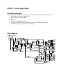
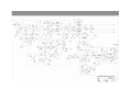
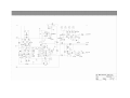
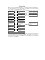
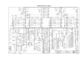
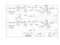
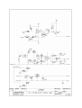
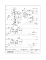
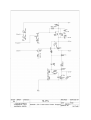
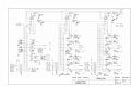
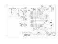
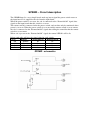
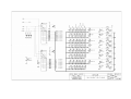
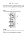
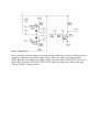
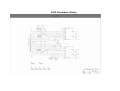
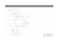
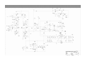
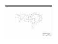
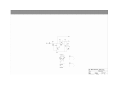
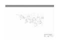
Line Extension
Circuit description and schematics for
C 20:8X
C 10:8X
C 10:4X
C 5:4X
Some of the schematics included here are not complete, or up to date. They should be used for educational
purposes only.
INDEX
INDEX ....................................................................................................................................... 2
SP20F – Circuit description ....................................................................................................... 4
Functional overview............................................................................................................... 4
Block diagram ........................................................................................................................ 4
Soft Start................................................................................................................................. 5
Stand-by (Auxiliary) supply................................................................................................... 5
Mains Detector ....................................................................................................................... 5
PowerGood_AUX .................................................................................................................. 6
PowerOn................................................................................................................................. 6
PFC......................................................................................................................................... 6
Resonant converter................................................................................................................. 6
PowerGood_2kW ................................................................................................................... 7
Service tips ............................................................................................................................. 8
SP20F Schematics .................................................................................................................. 9
AICO4b – Circuit description .................................................................................................. 13
Power supplies and power up/down..................................................................................... 13
Stand-by supply................................................................................................................ 13
Start-up ............................................................................................................................. 13
Local supplies................................................................................................................... 13
FanControl........................................................................................................................ 14
Control Ports ........................................................................................................................ 14
GPI ................................................................................................................................... 14
GPO.................................................................................................................................. 14
NomadLink....................................................................................................................... 14
Controller operation ............................................................................................................. 15
Controller ......................................................................................................................... 15
Analogue measurements .................................................................................................. 15
Digital measurements ....................................................................................................... 16
FanControl........................................................................................................................ 16
Signal flow ........................................................................................................................... 16
Input circuitry................................................................................................................... 16
Analogue control and monitor.......................................................................................... 16
Limiters ................................................................................................................................ 17
Clip limiter ....................................................................................................................... 17
Current Limiter................................................................................................................. 17
Average Current Limiter .................................................................................................. 17
Protections............................................................................................................................ 18
Turn off channels ............................................................................................................. 18
Low Impedance ................................................................................................................ 18
Short circuit ...................................................................................................................... 18
VHF.................................................................................................................................. 18
DC-Protection................................................................................................................... 18
Temp Protection ............................................................................................................... 19
DIP-switches ........................................................................................................................ 19
Service tips ........................................................................................................................... 20
AICO4b Schematics (Partly)................................................................................................ 21
SPSMR – Circuit description ................................................................................................... 29
SPSMR - schematics ............................................................................................................ 29
Front Panel ............................................................................................................................... 30
A10D – Circuit description ...................................................................................................... 32
Power supplies and power up/down..................................................................................... 32
Supplies ............................................................................................................................ 32
Power up........................................................................................................................... 32
Signal Flow .......................................................................................................................... 33
Enable/Disable of a channel ................................................................................................. 34
Protections............................................................................................................................ 34
VHF.................................................................................................................................. 35
DC-Protection................................................................................................................... 35
Temp Protection ............................................................................................................... 35
Crowbar............................................................................................................................ 35
Limiters ................................................................................................................................ 35
Clip limiter ....................................................................................................................... 35
Service Tips.......................................................................................................................... 37
A10D Schematics (Partly).................................................................................................... 38
SP20F – Circuit description
Functional overview
The power supply SP20F is used in the C-Series line extension amplifiers. It incorporates:
• Universal voltage input, 90-265 VAC
• Power Factor Correction (PFC)
• Soft start
• Fast mains unplugged detector
• A highly efficient isolated resonant converter for the high power outputs.
• A standby supply also used for lower voltages.
Block diagram
Soft Start
[PFC] When the mains cord is plugged into the wall, the following will happen:
The rectified mains will through D5 start to charge the capacitor bank C22-C25. The soft start
circuitry will make the capacitor tank charge slowly with low inrush current. R33 is used as a
current sense resistor and Q7 and Q4 is used to slow down this event. The voltage over the
capacitor tank will rise slowly, and after about 1-2 seconds it will have completed it’s inrush
cycle and R33 is bypassed via Q5, thus shorting the entire soft start circuitry. The node that in
the schematics is named 400V, will be Vin * 1,41 (for 220v Mains it will be ~311V, for 110v
Mains it will be ~155v). The circuitry will remain in this state until the external “Power On”
is activated from the input board (PWR_ON_CTRL).
Stand-by (Auxiliary) supply
When the capacitor tank has reached about 80VDC the standby supply will try to start.
[AUXILIARY] This converter is a self oscillating type and will change frequency depending
on its load. The high voltage (>80VDC) is fed through R76 & R77 and D13 will make sure
that the SOPS_STARTUP has a constant voltage of 12v. When the supply operates this
voltage will be supplied from the winding through D16, thus relieving the stress on R76 &
R77. This voltage will make Q10 conduct, thus making Q15 and Q12 to conduct. Now,
current flows through the primary winding, building up a magnetic flux. The current will
increase linearly with the time and so will the voltage over R62 & R78 current sense resistors.
When the voltage is enough it will trigger Q14 to conduct, thus making Q11 to discharge C85
and Q12 gate. This will stop the current in the primary winding, and the voltage polarity on
all transformer windings will reverse to discharge the magnetic flux. Mainly the transformer
discharges the flux to the secondary side, building up the voltage over the secondary
capacitors. During this time the voltage on pin 2 on the transformer will be positive, and
through C35 and R89 it will keep Q10 from conducting. When the flux in the transformer has
been discharged, the entire event will start all over again. D7 taps out a primary voltage
12V_Aux to be used on the primary side. Normally when IC5 optocoupler is not conducting
current, the transformer is charged with a high amount of energy, transferring all the energy
the transformer can handle. When the output reaches the desired voltages D49 will start to
conduct, driving current through the IC5 diode. This will alter the sensitivity on the current
sense circuitry, and make Q14 trigger on a lower primary current, thus transferring less
energy. This regulation will make the primary side not to put in more energy into the
transformer than we take out of it, thus keeping steady output voltages. When current flows in
the diode of IC5, Q13 will start to conduct current, thus making Pwr_AUX, that goes beyond
this page, to be -12v.
Mains Detector
[TOP] the Mains Detector is made up by IC1 and its surrounding components. When the
mains go above 80VAC (~113VDC) the voltage on IC1 pin 4 will go above 6,2v (D2) thus
making pin 2 discharge C7 rapidly. This will make pin 6 go below its reference thus making
its output high. This will slowly charge C8 through R3 and when it reaches 6,2v pin 14 will
go high, and the ENA will be high, thus bypassing the soft start and enabling the power
supply to turn on. During this time pin 13 will be close to 12v. If the mains cord is unplugged,
pin 13 will immediately go low, thus making the diode in IC2 conduct current, and disable
PWR_AUX to reach the PowerGood. To the input board this will signal a “PowerFail”
rapidly, thus making all circuitry turn off in a nice manner.
PowerGood_AUX
[TOP] When the standby supply has started and all auxiliary output voltages are stable Q1
will be pulled negative by the standby supply, as long as it’s not forced to ground by IC2.
This will make Q1 to be high impedance instead of shorted. The input board senses this and
uses this as a criterion for further startup.
Now we have reached this power supply state for standby. It will remain in this state until we
receive a “Power On” signal from the input board. This will only happen if the
PowerGood_AUX is high impedence.
PowerOn
[PFC]When the input board puts ~3,3v on the PWR_ON_CTRL node, the diode in IC4 will
conduct making the transistor in IC4 also conduct. If the ENA from the mains detector is high
this will make Q9 to conduct, which makes the 12V_ON to be 12v. If the ENA from the
mains detector is low, Q2 will conduct and prohibits Q9 from conducting.
PFC
The PFC is made up around IC3, which is the controller IC. The PFC controller is an advance
integrated circuitry and I will not go into detail about its regulator function. When it functions
as it should it should keep the capacitor tank (C22-C25) at 400VDC.
When the 12V_ON is close to 12v IC3 will have supply voltage and start to generate pulses to
Q3 via Q6 & Q8. When Q3 is conducting it will build up a magnetic flux in the coil L1. When
Q3 is not conducting, the coil L1 will discharge itself via D3 to the capacitor tank, making the
voltage over them be more than Vin*1,41. The main point of having a PFC is to make the
current in to the supply to be shaped as the voltage, thus making the supply look like a
resistive load on the mains. The controller ensures this by sensing the current by measuring
the voltage over R36 & R43. Since the current has to have the same shape as the voltage, the
IC3 also senses the voltage on the mains through R53. Several different regulators inside IC3
make the voltage and the current to have the same shape, sinusoidal on normal mains. The
controller senses the voltage on the capacitor tank through R42 & R38 and ensures it to be
400VDC.
Resonant converter
[Resonance] the resonance converter is a self oscillating circuitry. But unlike the previous
described standby supply, this converter will oscillate on the resonance frequency of the
capacitors C50, C51, C52 and the coil L7. The converter is made up by IC13 and it
surrounding components. When the 12V_ON is close to 12v IC13 will have supply voltage
through D26 and R92. It will then start to generate pulses to Q18 and Q19. I will not go
deeper into the primary side. There are 3 taps on the secondary side of the transformer,
+105v, -105v and a 13,5v that is referenced to the -105v. To keep the voltages steady D20
will control the current through IC6 and make sure that there are 210VDC between the -105v
and +105v.
PowerGood_2kW
[Resonance] When the +105v has reached ~80v the IC7 pin 3 will go above the (-) input thus
making it’s output pin 1 be high impedance. When the 13,5v reaches ~11v Q28 and Q27 will
make Q26 conduct current, thus enabling the -105v reach the PwrGood comparators in IC7.
When the -105v reaches about -80v, pin 6 on IC7 will go below its reference and the output
pin 7 will be high impedance. When both pin 1 & 7 on IC7 is high impedance Q34 will
conduct current, thus making Q35 gate negative making it to be high impedance. Thus the
PowerGood_2kW is released. This is sensed by the input board and when Q35 is not
conducting, this is interpreted as the resonance converter is up and running and the input
board can start all its functions. If the PowerGood_2kW is not released, the input board will
remain in standby.
Service tips
-
-
-
If the +/-105v (and the 13,5v) is very low although the switches Q18 and Q19 is
switching, you probably have short on the outputs. Please disconnect all outside
circuitry (by removing all amplifier fuses) to see if it starts up. When the outside short
has been found, continue repair there.
The PowerGood signal controls the power state on the input boards, and the power
state on the entire device. So start by checking these. They should be above 2v to
signal good. If they are below, they signal fail.
If the resistors R62 and R78 in the auxiliary supply have opened, the entire primary
will end up in an “in-between” state instead of switching between on and off. If the
auxiliary supply is not switching, check these before going into deeper fault localizing.
SP20F Schematics
AICO4b – Circuit description
Power supplies and power up/down.
Stand-by supply
The power supply in the unit has a standby supply which is always on when the mains cord is
plugged in. Once this converter has enough supply to generate good output power it will
generate a “PowerGood_Aux”, which will go high. Before this it can only be powered
through NomadLink.
[NLIPs] When a Voltage is present on NomadLink it will go through D407 and if the standby
supply is off it will go through Q410. When the standby supply is on, it’s PowerGood will,
through Q422, turn off Q410 and feed +12v from the standby supply through D408 to the
same node. The existence of Nomadlink power is sensed through R475 and R472, and when
this is high it will activate the Com-Led by pulling the ComCt high. This will turn on Q416
and turn off Q411, thus leading the current through the Nomadlink diode which is connected
between Com+ and Com-.
Q412 & Q414 forms a current limited +5v regulator. This is biased from R481. When the
voltage over R482 exceeds 0,6v the regulator will lower its output voltage until the current
remains constant. This +5vP supplies everything that needs to be on in standby, most
important the controller U407. [UPcB] The controller uses a lower voltage to operate, and this
is made through Q409 that will make the voltage be 3,0 – 3,6 V. [LVPsB1] In standby all
other voltages is turned off by Q401 and Q408.
Start-up
There are 3 different ways to turn on this amplifier; by NomadLink command, by GPI (only
when Nomadlink is disabled by dip switch) or on the front switches. The Controller will scan
the front switches for On/Off & Remote. Manual – on or off will directly generate and
internal request to turn on (or off) the PSU. When in Remote the same request will come from
either Nomadlink or GPI (depending on the switches). This internal request will be generated
to the PSU When “PowerGood_Aux” is high. This means that if the standby supply is not on,
then the controller will not start the amp.
When the standby supply is on and a Power On is requested the Controller will pull PwrOnCt
high and the power supply should start shortly after. When the supply has reached sufficient
output voltage it will release the PwrGood105V.
Local supplies
When PwrGood105V is high, the controller will wait about 0,6s before doing anything, and if
all is ok, it will then go over into operate-mode.
[LVPsB1] When PwrGood105V goes high, Q406 & Q402 will turn on and turn on Q408 and
Q401. U403 will regulate the voltage between -18 - +18 to be 35,5v – 35,9v (if they are not,
adjust VR401 until they are). Since this voltage from the supply is floating, U401 sets its
reference to ground to be exactly at 50% of this voltage. U401 will push and pull Q405 &
Q403 until AG is equal to the voltage division R408 and R410. This makes the +/- 18v.
U406 is a +5v regulator which will generate a local +5v (this is not the same as +5vP standby
voltage!).
FanControl
[LVPsB1] U402 & Q404 forms the Speed control circuitry for the fans. It is basically an
inverting amplifier that can open and close Q404 through D401. If the FanCt (from the
controller) is kept high the fans will be at low speed. During power on the fans will start up
with a high voltage to get them running, this is done by C409 being discharged at the
beginning. The controller measures the temperature on the amplifier modules. And if they go
above ~40deg C, the controller will lower the voltage on C409 by Pulse Width Modulating
the FanCt signal.
Control Ports
GPI
[NLIB/GPIO] the GPI ports are used to power on/off the amplifier if the criterion for this is
met. This is; if front switches are Remote - On. The DIP switch is set to GPI.
The circuitry for GPI 1 and 2 are identical. If GPI1a and GPI1b are connected to each other,
current flows through Q427. This opens Q421 and pulls this down through R486. This signals
to the controller that the GPI1 is activated. During normal mode, by closing these connectors
for more than 100ms will make the amp go on and when closing them again a second time the
amp will go off. The same goes for GPI2.
By activating the dip switch “GPI2 level trig” GPI1 is discarded. By closing GPI2 for more
than 100ms the amp will go on. When opening GPI2 for more than 100ms the amp will go
off.
GPO
[NLIB/GPIO] There are 2 semiconductor relays that control the GPO ports. By driving
current through the diode the relay closes. The GPO2 is connected to the local +5v, so this
will be activated as soon as the amplifier is on. The GPO1 is connected to the controller serial
circuitry and will be activated by the controller when there is a fault on any channel.
NomadLink
[NLIB/GPIO] NomadLink is a transformer isolated serial communication network.
Communication that comes into the IN port will only reach this device. Communication on
the Out port will be directly transferred to the IN port. U417 has the capability to electrically
exchange these ports so they switch functionality with each other. This is done when devices
receives communication on the Out port only, and is controlled by the controller N/R pin, ~0v
means normal, ~3,3v means switched ports. When NomadLink is turned off by the dip
switches, the controller pulls NMLOn* to ~3,3v. This disables the NomadLink completely by
opening all the switches inside U417. The NMLOn* should be close to 0v normally.
[UPcB]When no communication is present (NML cable unplugged), the processor’s
transmission pin (Tx) pin will be internal disconnected and will be ~1,65v because of the
voltage division between R461 and R470. [NLIB/GPIO] this voltage will be gained in
U413(1,2,3) to be ~2,5v which will go through R473, through the transformer and end up at
C432. U413(5,6,7) will in this state only transfer the 2,5v DC to it’s output, and through
R462, through the transformer and to C433. U414 will detect any communication and in idle
it will leave a high output of about 3,3v. During communication all these voltages will have
an AC square wave signal on them, and it requires a digital storage oscilloscope to analyze
them. If the DC voltages are correct, then it usually works.
Controller operation
All levels on the IO pins on the controller is interpreted as <1v low (‘0’) and >2v as high
(‘1’). Any input that is more than ~4,5v is hazardous to the controller pin.
Controller
The first criterion for the controller operation is that it has operating voltage on pin 5, 17 and
38. This should be over 2,7v (usually between 3,0 – 3,6v). The second criterion is that the
RESET pin (4) is high. The third and final criterion is that the controller has a clock source.
This could be measured on pin 8 of the controller using an oscilloscope. The wave shape does
not need to be a perfect square wave shape; it looks more like a triangular wave. But it should
run at the frequency of 7,37 MHz.
During standby the controller uses the following pins:
NMLOn*
Out-port low -> NomadLink on, high -> NomadLink Off
GPI Level
In-port, Reading on dipswitch.
GPIMode
In-port, Reading on dipswitch.
GPI1
In-port, Reading on GPI1 state.
GPI2
In-port, Reading on GPI2 state.
PwrOn/off
In-port, Reading on Power On/Off switch state.
RemOn/Man
In-port, Reading on Remote On/Off switch state.
NML
Out-port, NomadLink direction. low = normal, high = switched
PhSen
In-port, high when NomadLink is connected
Int0
In-port, PowerGood_Aux sense.
Int1
In-port, PowerGood_105v sense.
ComCt
Out-port, controls ComLed, low =ComLed not lit, high =ComLed lit.
MuteAll
Out-port, when low all channels forced silent.
PwrOnCt
Out-port, when high the main PSU should start.
When the controller goes into operating mode, 3 additional functions is started in the
controller:
Analogue measurements
The Analogue measurements will start, for this to happen, the analogue to digital converter in
the controller needs to be supplied. This is done via R436 to pin 27. This should be the same
as the controller supply voltage (3,0 – 3,6v). The A to D converter also requires a reference
voltage to function properly; this should be 2.49v – 2.51v and could be measured at pin 29.
U405 (on top schematics) will route the analogue level on its input pins to the controllers,
AdIn pins, which are analogue input pins. The controller decides which input that will be
measured by changing the states on AMux 0:2.
Digital measurements
The digital data gathering interface will start. Clk, MISO, MOSI and CS will go through
U409 & U411 to convert it to 5v logic. When CSA-D is pulled low (<1v) then Clk, MOSI &
MISO will be routed to the lower board circuitry (containing the information for ch A-D) and
to the front panel. When CSE-H is pulled low, then Clk, MOSI & MISO will be routed to the
higher board circuitry (containing the information for ch E-H). The data gathering line
consists of a number of shift registers connected in series (U1, U101, U201….). when CS
goes <1v it will take a sample of the data on the input pins, and when a clock pulse are sent to
them, they will shift their data one step closer to the controller. The controller will shift it into
its memory in the same manners. After all data has been shifted in, the controller stores the
value as a representation of what’s happening on the channels. The same goes for data shifted
out of the controller. When CS goes >2v the inputs will be ready to receive new data, and the
outputs will be what the controller shifted to them.
FanControl
The analogue measurements on the temperature on the modules will yield a specific fan value.
When the temperature is below 40deg C the fans will be at idle, and FanCt should be close to
3,3v. Between 40 and 60 deg C the fans will be temperature controlled, the higher the
temperature, the lower the voltage. When the temperature exceeds 60 deg C the fans will go at
maximum, and FanCt should be close to 0v.
Signal flow
Input circuitry
[AIG2B] The input circuitry is made up by U6 and U5. U6(5,6,7) is an inverting amplifier and
its gain is -1 through R58 & R59. This is fed into a summing amplifier U6 (1,2,3). This
amplifies signals with the same phase through R56 & R57. Its gain is set by R48 and
depending on Q18 can be -6dB (Q18 off) or 0dB (Q18 on). This -6dB switch only exists on
Ch A, C, E, G and is only used when bridging 2 channels (in bridge mode, Ch B, D, F, H
input circuitry is not used).
U5(5,6,7) is when Q32 is on an inverting amplifier with gain ~ -1. Q32 is opened by selecting
35Hz high pass filter on the dip switches, this causes C34 to form a 35Hz high pass filter.
U5(1,2,3) is preceded with a damper network formed by R54, R53 & Q15 (R52 is added to
keep Q15 from distorting the signal when opened). When Q15 is on this network damps the
signal 3dB and 0dB when Q15 is open. This signal is fed into U5(1,2,3) which has a gain set
by R42, R41 & R40, if Q14 is open. When Q14 is closed R40 is shorted and electrically
omitted. U5(1,2,3) has Gain +3dB when Q14 is open and +9dB when Q14 is closed. Q15 and
Q14 are controlled by the gain switches on the rear on the amplifier.
Analogue control and monitor
[ACM1A] the signal goes through the front panel attenuators, and into the ACM1A schematic
page. It goes through R31 to U2(1,2,3). U3 is an automatic limiter component. By running
current through its diode, the signal is limited. During normal operation there shall be no
current going through this diode, and this component has no affect on the signal. U2(1,2,3) is
a non-inverting amplifier and sends the signal out of the block again.
On the top schematics we can see that on ch A and C they are fed directly back in. On ch B
and D they go through a relay (RE401, RE402). This relay is activated when bridging 2
channels. When Ch A & B are bridged Ch A’s input signal is fed to Ch B but in opposite
phase.
The signal then goes to U2, which is a balanced amplifier. It senses the signal ground on the
amplifier modules and cancels them out. This rejection is trimmed in production by tuning
VR1.
After the amplifier modules the signal comes back trough the output filter coil K1. This coil
has an extra winding on it, and it is used to sense the current that goes to the speaker. This
signal is fed into the amplifier U7, which compensates for the frequency dependency in the
coupled coil K1. On the output of this amplifier is a signal that should be in direct proportion
to the current going to the speaker.
Limiters
Clip limiter
Whenever the UClip signal is pulled low, and Clip mode is set to soft (dip switch – enables
Q5 to lead current) there will go current through the LED in U3, thus limiting the signal. The
clip limiter is made up of 2 circuitries. When the VPL is set at the highest voltage, the
amplifier module will clip whenever the output signal reaches the rail voltage. If this is the
case, the amplifier module will pull down the UClip to ground. When the VPL switches are
set to a lower voltage, it will generate a DC voltage VclCt that is fed into U4. Whenever the
signal on U2:3 goes above this, Q13 will pull the UClip signal to ground. When UClip is
detected the signal is also fed to the shiftregister U1(13) through a diode. This tells the
controller that the channel clips.
Current Limiter
The Isen signal (output from U7) is a representation of the current going to the speaker. This
is fed into U10(4,7). This circuitry is a window comparator, and when the signal exceeds the
+/- voltage over R90, the output U10(1,2) will go to -18v. This triggers Q27 and Q25 to
conduct current, thus pulling the Ilim signal low. This will through R28 and D2 lead current
through the diode in U3, thus limiting the signal. When ILim is detected the signal is also fed
to the shiftregister U1(14) through a diode. This tells the controller that the channel current
limits.
Average Current Limiter
The Isen signal is fed into D1 to rectify the signal. When this signal has amplitude enough it
will charge C29, fairly slowly. If this signal is sustained for about 200ms C29 has been
charged enough to trigger Q16 to limit the signal. When this detector is active the signal is
also fed to the shiftregister U1(7). This tells the controller that the channel limits.
Protections
Turn off channels
To turn of a channel, 2 things need to happen. The signal needs to be lowered, and this
happens when the controller sends out mute to the channel. This will trigger Q4 to draw
current through the diode in U3. Shortly thereafter Q21 pulls down the En_A signal going to
the amplifier modules, thus turning off the output transistors. There is a short delay between
the signal is limited to the output stage shuts down. This delay is to make the shutdown sound
more nicely, and is made out of D8, R47 & C25. There is also a feedback signal telling that
the channel has been muted through R50. This is fed into the shift register U1(6).
Low Impedance
The controller samples the input level on its analogue to digital converter. It also receives
signal on the shift register when the channel is in current limiting. When the controller detects
that a channel is in current limiting, it will then check the voltage input, and if the voltages is
so low that there must be a load <1 Ohm on it, it will turn off the channel for 6 second. The
controller will during this state lit up the CPL diode on the front.
Short circuit
Since the current limiter is fairly slow (attack time of ~1ms) there is a possibility that short
high frequency spikes could pass through the amplifier. This could be dangerous to the output
transistors, so there is an additional protection for this. The ISen signal is fed into U10(8,11)
and compared to the +/- voltage over R89. This should happen when the output current
exceeds 30Apk. If that is the case, then the outputs U10(13,14) will go to -18v. This will turn
on Q29, Q23 & Q26 this will immediately shut off the output transistors. Instantaneously Q22
and Q28 will be triggered and tell the controller that this protection has kicked in. The
controller will then mute the channels (although they are already off), and then release
everything 6sec after. The controller will keep the LED CPL constantly lit on the front during
this state.
VHF
The VHF protection is located on the amplifier module, but when it is activated the En_A will
go low. This is fed into the shift register U1(1) and when this has been pulled low while Mute
and short circuit is inactive, then it will be interpreted as a VHF protection. The controller will
keep the channel muted for 6s and lit up the VHF led on the front.
DC-Protection
When DC appears on the output a protection circuitry on the amplifier module will kick in
and destroy the channels fuses. When this happens the DCProt signal (which normally should
be close to 0v) will go either positive or negative from the amplifier modules (depending on
which fuse (or both) that has been destroyed). This will trigger Q3 and send the information to
the controller. The controller will shut off the channel (mostly to prevent any further damage).
The controller will indicate FAULT on the front by lighting up the VHF and CPL.
Temp Protection
On U405 (top schematics) the channels temperature is monitored. On the amplifier modules
there are a temperature dependent resistor that is mounted on the cooler. This will together
with the impedance network R1, R430 translate to a voltage that is proportional to the
temperature. If the voltage on U405(1,5) goes below 0,5v this means that the temperature on
the module have reached ~100deg C, then the controller will shut down the channel until it
reaches ~90deg C. the controller will also lit the Temp led on the front to indicate this.
DIP-switches
The HP Filter switch is read by the controller through the shift register. It will also generate a
0v / -18v to the JFet switch.
The Clip Mode switch is read by the controller through the shift register. It will also pull
down the 5v to ground, thus turning off the UClip signal to the automatic attenuator.
The VPL switches is read by the controller through the shift register. These switches will
generate a DC- voltage that is used by the VPL circuitry to clip the signal at the correct level.
The Bridge switch is read by the controller through the shift register. It will also feed +5v to
the relays that routes the signal to the other channel. Also it will generate a 0/-18v to trigger
the -6dB JFET on the input circuitry.
The GAIN switches is read by the controller through the shift register. They are also used to
generate 0 /-18v to the JFets in the input circuitry to set correct gain.
FAN Masked switch is read by the controller through the shift register. It is used to make the
controller to count in the output sound pressure to control the fans.
The GPI Level and Mode is sent directly to the controller, since it needs to be sensed even in
standby.
Service tips
-
-
During service of an 8 channel amplifier, it is safe to remove the AICO4bExt board
from the AICO4b board and run the amplifier only with the lower board. You do not
need to disconnect the Ch E-H amplifier module.
If the amplifier does not start up, set it to Manual-On and follow the scheme below:
+12v from supply?
no
continue repair on
supply
yes
Is +5vP ok?
Faulty +5vPh regulator
[NLIPs] or shorted 5vPh
High
no
check PwrGood_Aux
continue repair on supply
low
yes
+9v from supply?
yes
Pin 42 high and 43
low on U407?
yes
no
continue repair on
supply
no
check connection to
the power switches
PwrOnCt High?
no
yes
PwrGood_105v
high?
yes
+/-18v & +5v ok?
check controller
operation
no
continue repair on
supply
no
repair regulators in
[LVPsB1]
ok
Connect the device to
NLB60E and check the
software
yes
The board should be powered up.
-
If the communication led is blinking rapidly (~3 blinks every second) instead of once
every other second, when connected to a NLB60E. The controller is stuck without
valid software. Please contact LAB.Gruppen service department on how to download
new software to the amplifier.
AICO4b Schematics (Partly)
SPSMR – Circuit description
The SPSMR board is a very simple board, made up just to signal the power switch states to
the input board. It is supplied with +9v from the input board.
When the power switch is set to on, the +9v is connected to the “PowerOn/Off” signal, thus
signals to the input board that this switch is set to on.
The remote switch is connected after the power switch, and can thus only be monitored when
power is set to on. When the power switch is set to on and the remote switch is set to remote,
the +9v is connected to the “RemoteOn/Off” signal, thus telling the controller that the remote
switch is set to remote.
When +9v is present at the “RemoteOn/Off” signal, the remote LED D1 will be lit.
Below truth table will give the signal value for each switch:
Power
Remote
“PowerOn/Off” “RemoteOn/Off”
Off
Manual
0v
0v
Off
Remote
0v
0v
On
Manual
9v
0v
On
Remote
9v
9v
SPSMR - schematics
Front Panel
The front panel is controlled from the controller on the input board. All diodes except for one,
the NomadLink LED, works in the same manners. The NomadLink LED is supplied from the
input board, so it has the ability to be lit even when the front panel registers are not powered
(as in standby or off).
The front panel is an extension to the AICO4b board shift registers, but they are also supplied
with an En (Enable) signal. This signal, when pulled low, makes all shift registers output
high-impedance. This En signal is mainly used upon boot up to make sure that the registers
contain valid data before releasing current through the LED’s.
The controller drives the LED’s by at the same time feed the registers with data for a given
row of LED’s (1-7) together with the intended row (ChA – ChH) selector. When a row is
selected the corresponding ChX pin is driven low, this enabling the transistor for that row (Q1
– Q701) to conduct current. When a row has been updated the controller moves on to update
the next row and when it’s finished with all rows, it starts all over again.
A10D – Circuit description
The A10D Amplifier board incorporates a 4 channel high power audio amplifier. The board is
build up as 2 stereo amplifiers. Most supplies are shared between the 2 channels and split to
the next 2 channels. The A10D is a class D amplifier, and the operation of a class D amplifier
differs a lot from class A, B, AB or H amplifier. Instead of amplifying the signal using
resistive elements, the output is generated by 2 switches that are either on or off.
Power supplies and power up/down.
Supplies
The Amp-modules requires several supplies. The +/-105V and 13.5V are split in two, one for
each pair of channels. Each of the four channels has their own +/-12V supply.
Furthermore for each channel +/-5V is generated on the module.
+12V
+5 V
AGND
-12V
-5V
-105V
AGND
+13.5V(Ref to -105V)
-105V
+12V
+5 V
AGND
-12V
-5V
+12V
+5 V
AGND
-12V
-5V
-105V
AGND
+13.5V(Ref to -105V)
-105V
+12V
+5 V
AGND
-12V
-5V
Figur 1 – Power supplies
Power up
If the +13.5V is not present on a channel it won’t operate at all. The voltage can be measured
at the driver at TP88(TP103, TP304 and TP319). Remember that this voltage is referenced to
-105V.
If any of the 6 remaining supplies is missing there might be some switching but the switching
frequency won’t be correct. It is most likely that there will be no switching at all.
The switching frequency can be measure on the power PWM at TP101(TP116, TP317 and
TP332) and should be between 400kHz and 500kHz square wave reaching from +105v to 105v. It is important that this square reaches the positive and negative rail, otherwise the
transistors are not completely on and they will get very hot.
+/-12V can be measured at the OpAmp (IC13 , IC22 , IC9 and IC10) on the supply pins 4 and
8 respectively.
+/-5V can be measured at the OpAmp (IC5 , IC21 , IC14 and IC19) on the supply pins 4 and
8 respectively.
+/-105 should be measured at the amp-side of the fuses on the top-side of the PCB.
These 6 supplies are all referenced to AGND.
Signal Flow
[TOP] The signal enters the board through the ribbon cable. For Ch A the signal is located on
pin 4 (ground) and 5 (signal). It then goes into the feedback schematics. [FEEDBACK]. The
signal goes into the balanced receiver IC13(1,2,3). The output pin 3 is fed into the high
frequency amplifier IC5(1,2,3) and then IC5(5,6,7). At this point the signal is a square wave.
It is then fed into the comparator IC1 and through the gates IC6 & IC7. Up to this point all
signals can be measured using an oscilloscope connected to ground. Q7 & Q8 transfer the
pulses to -105v so to continue to follow them beyond these transistors requires that you
ground the oscilloscope in the -105v (beware if the scope is grounded in chassis ground,
connected in a grounded mains or similar you could short the -105v to ground this way, and
possibly destroy the oscilloscope and/or the amplifier).
[POWERGAIN] the pulses reach the driver IC11 pin 1 and 2. The driver generates output to
turn on or off Q10 according to the pulses on pin 1. This is made by driving pin 5 to about
10v over -105v. Q4 and Q5 amplifies the current so the transistor turns on and off fast
enough.
The driver generates output to turn on or off Q9 according to the pulses on pin 2. This is made
by driving pin 7 to about 10v above the output signal. Q3 and Q6 amplifies the current so the
transistor turns on or off fast enough. To measure this signal, the oscilloscope must be
grounded on the TP101. When Q9 is on TP101 is ~+105v, which means that the driver must
supply +105v + 10v (=115v) to Q9 to keep it conducting. This is done by having a capacitor,
C38 connected to the switching node TP101 that charges itself when Q10 is on. D24 makes
sure that C38 is never charged to more than 15v. this voltage is then used to supply the output
driver IC11 pin 8, and to supply the driver transistor Q3.
Enable/Disable of a channel
Figur 2 - Enable circuitry
To be able to disable/enable the amplifier two 2-input NAND gates have been implemented.
If the ENABLE is pulled low the output of the NAND is high. When the enable pin is
released (the module has a pull up resistor to +5V) the NAND gates just operate as inverters
on the signal from the comparator TL3016.
Protections
On the Amp-module different protections have been implemented on each channel:
• VHF
• DC
• Temp(PCB)
These three protections (VHF, DC and Temp) all pull the ENABLE LOW. Well not
completely to 0V but to about 0.6V. By measuring the ENABLE voltage you can determine if
the Amp-module protects itself (ENABLE=0.6V) or it is disable from the input-board (0V).
A special case is if short-circuit has occurred. Then the ENABLE voltage is pulled LOW
(0.6V) by the AICO-board and the Ilim LED is constantly lit on the front.
Figur 3 - Protections circuitry
VHF
If VHF occurs on the output the voltage over C224 (C125, C209, C108) goes up and triggers
the latch Q47 (Q20, Q41, Q22).
DC-Protection
If low positive DC occurs for some seconds the voltage over R275 (R302, R257, R88) goes
up and triggers the latch Q49 (Q40, Q43, Q23). If negative DC occurs for some seconds the
voltage over R276 (R318, R258, R89) goes up and triggers the latch Q49 (Q40, Q43, Q23).
Temp Protection
If the temperature on the PCB reaches approximately 100degC the voltage over R296 (R300,
R123, R293) goes up and triggers the latch Q59 (Q60, Q28, Q30).
Crowbar
For safety reasons each channel has a crowbar in case an output Power MosFET is shorted.
When high DC appears on the output a protection circuitry will kick in and destroy the
channels fuses. At the same time the FUSEN goes HIGH or LOW .
Limiters
Clip limiter
The amplifier module will clip whenever the output signal exceeds the rail voltage. If this is
the case, the amplifier module will pull down the UClip to ground.
Figur 4 - Clip detector
In case the Amp is in hard clip the error signal in the feedback goes above normal level in the
attempt to compensate the lack of output voltage. This error signal is fed through R235
(R224, R69, R3) and compared to supply voltage dependant limits at IC20 (IC18, IC12, IC2).
When clip is detected by IC20 (IC18, IC12, IC2) output goes high and it makes Q56 (Q53,
Q26, Q1) pull the Vclip to ground.
Service Tips
•
•
•
Always make sure that the supplies and the EN signal is correct.
If the amplifier fuses are continuously blown, remove the output FETs and exchange
the fuses. Set the input board to hard-clip mode and feed the channel with a 1 kHz sine
wave (VPL indication on the front is normal in this case). Instead of high frequency
pulses you should now have 1 kHz square wave pulses. Follow the pulses on the board
and see where they stop.
If the amplifier is continuously in VHF protection, then it should retry every 6 second
(seen as a short blink on the front). If not, then the protection circuitry is faulty.
A10D Schematics (Partly)