1
HEWLETT
PACKARD
OPERATION AND SERVICE MANUAL
MODEL 4192A
LF IMPEDANCE ANALYZER
SERIAL NUMBERS
This manual applies to instruments with
serial numbers prefixed
2150J·
and above.
©
COPYRIGHT: YOKOGAWA-HE WLETT-PACKARD, LTD" 1983
9-1, TAKAKURA-CHO, HACHIOJI-SHI, TOKYO, JAPAN
Manual Part No.
04192-90001
04192-90050
Microfiche Part No.
Printed:
APR.
1984
Section I
Model 4192A
Paragraphs 1·1 to 1-5
SECTION I
GENERAl. INfORMATION
1 - 1.
1-4.
INTRODUCTION
1-2.
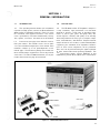
This operating manual contains the information
required to install, operate, and test the Hewlett-Packard
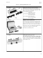
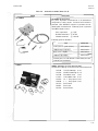
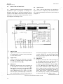
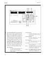
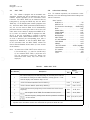
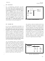
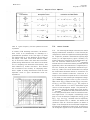
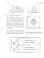
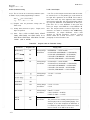
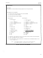
Model 4 1 92A LF Impedance Analyzer. Figure I-I shows
the instrument and supplied accessories. This section
covers specifications, instrument identification, descrip
tion, options, accessories, and other basic information.
1-3.
Listed on the title page of this manual is a micro
fiche part number. This number can be used to order
4 X 6 inch microfilm transparencies of the manuaL Each
micofiche contains up to 60 photo-duplicates of the
manual pages. The microfiche package also includes the
latest manual changes supplement as well as all pertinent
service notes. To order an additional manual, use the part
number listed on the title page of this manuaL
DESCRIPTION
1-5.
The HP Model 4 1 92A LF Impedance Analyzer is
a fully automatic, high performance test instrument
designed to measure a wide range of impedance para
meters as well as gain, phase, and group delay. The
4 1 92A improves efficiency and quality in the develop
ment and production of many types of complex compo
nents, semiconductors, and materials. Complete network
analysis of devices such as filters, crystals and audio/video
equipment, plus evaluation of the impedance character
istics of their circuit components, can be performed.
These tests can be performed using test signals equivalent
to those found under actual operating conditions. The
two measurement display sections, DISPLAY A and
DISPLAY B, provide direct readout of the selected meas-
11170A
04192-6 1 00 1
Figure 1�1.
8120-1378
Model 4192A and Accessories
I-I
Section I
Paragraphs 1·6 to 1·9
urement parameters with 4V2 digit resolution along with
the appropriate units. In NORMAL mode operation, the
4 1 92A performs approximately five measurements per
second. The 4 1 92A also provides an AVERAGE meas
urement mode (approximately one measurement per
second) to obtain measurement data of higher resolution
and repeatabily than is possible in NORMAL measure
ment mode, and a HIGH SPEED measurement mode to
perform approximately ten measurements per second.
delay is 0. 1 ns to 1 9.999s with a resolution of 4\1, digits.
These features make accurate measurement of transmis
sion characteristics easier than ever before. For example�
0.001 dB changes in insertion loss and ripple in the pass
band of a BPF (Band Pass Filter), caused by temperature
changes, can be resolved. Moreover, the ability of the
4 1 92A to measure group delay helps in the design and
construction of filters that must accurately transmit
phase information.
1-6.
'The 4 1 92A can provide measuring frequency,
OSC level, and de bias voltage (impedance measurements
only) equivalent to actual operating conditions. The
sweep capability of the built-in frequency synthesizer and
dc bias source permits quick and accurate measurements.
The b uilt-in frequency synthesizer can be set to meas
uring frequency within the range from 5.000Hz to
1-8.
In impedance measurements, the 4 1 92A can
measure eleven impedance parameters - absoktte �e of
impedance (I Z I), absolute value of admittance (IYI),
phase angle (0), resistance (R), 'reactance (X), con
ductance (G), susceptance (B), inductance (L), capaci
tance (C), dissipation factor (D) and quality factor (Q).
Measurement range of I Z I /R/X is 0 . 1 mn to 1 .2999Mn .
I Y I /G/B is I ns to 1 2.999s; 0 is - 1 80.00' to +1 80.00' ;
L is O . O l mH to 1 .000kH; C is O. l pF to 1 00.OrnF; D is
0.0001 to 1 9.999; Q is 0 . 1 to 1 999.9. All have a basic
accuracy of 0. 1 % and a resolution of 4Y2 digits (number
of display digits depends on measuring frequency and
OSC level setting). Moreover, the unique circuitry of
the 4 1 92A provides direct and accurate impedance
measurements of both grounded and floated devices.
1 3. 00000MHz with I m Hz maximum resolution. OSC
level is variable from 5 mV to 1 . 1 Vrms with 1 mV resolu
tion ( 5 mV for levels higher than lOOmV). The internal
d c bias voltage � 'urce (impedance measurements only)
provides ± 3 5 V in I O mV increments. Measuring fre�
quency or dc bias voltage can be automatically or manu�
ally swept in either direction. OSC level can be manually
swept in either direction in 1 mV increments (S mV for
levels above 100mV). Actual test voltage across- or test
signal current through the device under test is also
measured. Thus the 4 1 92A can evaluate components and
circuits under a wide variety of measurement conditions.
For example, video frequency characteristics of a VTR
head, dc bias voltage characteristics of a semiconductor
or ceramic device, at circuit level as well as component
level, can be accurately evaluated. For measurements on
high Q ('" 106) devices or for impedance measurements
that require a test signal that is more stable than that
provided by the 4 1 92A, an external frequency synthesizer
can be connected to the 4 1 92A EXT VCO input con
nector. Using this technique, a frequency resolution of
ImBz over the full frequency range, from 5Hz to 1 3MHz,
can be obtained. In addition, a high stability reference
( l MHz or 1 0MHz) can be connected to the 4 1 92A so
that even more-stable test signals are obtained.
1-7.
In amplitude/phase measurements, the 4 1 92A can
measure four transmission parameters - gain/loss (B-A),
level (A, B), phase (0), and group delay. Measurement
range of B A is - IOOdB to + I OOdB with 0.00 1 dB
maximum resolution and 0.02dB to 0.09dB basic ac
curacy ; measurement range of A/B is +0.8 dBV to
-lOOdBV, + 1 3. 8 dBm to -· 8 7 dB m with O.OO l dB maxi
mum resolution and OAdB basic accuracy; measurement
range of 8 is - 1 80° - + 1 800 with 0.0 1 ° resolution and
0. 1 0 to 0.20 basic accuracy ; measurement range of group
1-2
1-9.
The 4 1 92A employs certain functions which
make the best use of the intelligence capability of its
microprocessor. This microprocessor-based design of the
hardware makes operation of the 4 1 92A simple, yet
improves performance to realize the accurate measuring
capabilities. Desired test parameters are fully program
mable through the front-panel control keys or via HP-lB
control, a standard capability of the 4 1 92A. The devia
tion measurement function eliminates the need for
tedious deviation calculatjons. Deviation measurement
can be performed on all measuring parameters and is
displayed as either the deviation (LI) from a stored refer
ence value or percent deviation (.6.%). This feature is
useful for environmental tests such as temperature
characteristics measurement of filter loss, and gain vs.
frequency for amplifiers. The self test function augments
the high reliability design of the 4 1 92A. Convenient
introspective testing is possible by pressing the SELF
TEST key and confirms the functional operation of the
instrument. The zero offset adjustment function meas
ures the residual impedance and stray admittance in
herent to the test fixture used, and offsets the effects of
these parasitic parameters to zero with respect to the
measured values. The save/recall function can store
(SAVE key) five completely different front-panel settings,
including both parameter selection and sweep controls,
and recall them at any time (RECALL key). This feature
Section I
Model 4192A
Paragraphs 1 · 1 0 to 1·21
improves efficiency in production applications where
repetitive measurements are made. This feature can also
b e used to measure the same parameter on one com
ponent under (five) different sets of test conditions. The
standard memory of the 4 1 92A preserves stored data
even when the instrument is off.
1 - 1 0. The 4 1 92A provides HP-lB interface capability
for complete remote control of all front-panel control
key settings and test parameter settings. This feature
makes it possible to integrate the 4 1 92A into a measure
ment system which reduces cost b y improving DUT
throughout, improving circuit design efficiency, and
shortening the component development period. The
4 1 92 A is also equipped with X-Y recorder outputs and
pen lift eontrol. Clear and accurate copies of character
istics curves resulting from swept measurements can be
obtained easily with this capability, without an external
HP-lB controller.
1 - 1 1 . The versatility and operability of the 4 1 92A are
maximized by the availability of versatile test fixtures.
Because components and networks are not of uniform
shape and Slze, the 4 1 92A has several test fixtures that
can be used to best meet different measurement require
ments.
1 - 12.
SPECI F I CATIONS
1 - 1 3 . Complete specifications of the Model 4 1 92A LP
Impedance Analyzer are given in Table I - I . These specifi
cations are the performance standards or limits against
which the instrument is tested. The test procedures for
the specifications are covered in Section IV, Perfonnance
Tests. Table 1-2 lists supplemental performance charac
teristics. Supplemental performance characteristics are
not specifications but are typical characteristics included
as additional information for the operator. When the
4 1 92A LP Impedance Analyzer is shipped from the
factory, it meets the specifications listed in Table 1 - 1 .
1 - 1 4.
SAFETY CONSIDERATIONS
1 - 1 5. The Model 4 1 92A LP Impedance Analyzer has
been designed to confonn to the safety requirements of
an IEC (International Electromechanical Committee)
Safety Class I instrument and is shipped from the factory
in a safe condition.
1 - 1 6. This operating and service manual contains in
formation, cautions, and warnings which must be followed
by the user to ensure safe operation and to maintain the
instrument in a safe condition.
1-17.
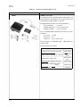
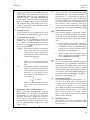
INSTRUMENTS COV E R E D B Y MANUAL
1 - 1 8 . Hewlett-Packard uses a two-section nine character
serial number which is stamped on the serial number
plate (Figure 1-2) attached to the instrument's rear-panel.
The first four digits and the letter are the serial prefix and
the last five digits are the suffix. The letter placed be
tween the two sections identifies the country where the
instrument was manufactured. The prefix is the same for
all identical instruments; it changes only when a change is
made to the instrument. The suffix, however, is assigned
sequentially and is different for each instrument. The
contents of this manual apply to instruments with the
serial number prefix(es) listed under SERIAL NUMBERS
on the title page.
1 - 1 9. An instrument manufactured after the printing of
this manual may have a serial number prefix that is not
listed on the title page. This unlisted serial number pre
fix indicates the instrument is different from those
described in this manuaL The manual for this new instru
ment may be accompanied by a yellow Manual Changes
supplement or have a different manual part number. This
supplement contains "change information" that explains
how to adapt the manual to the newer instrument.
1-20. In addition to change information, the supplement
may contain information for correcting errors (called
Errata) in the manual. To keep this manual as current
and accurate as possible, Hewlett-Packard recommends
that you periodically request the latest Manual Changes
supplement. The supplement for this manual is id :ntified
with this manual's print date and part number, both of
which appear on the manual's title page. Complimentary
copies of the supplement are available from Hewlett
Packard. If the serial prefix or number of an instrument
is lower than that on the title page of this manual, see
Section VU, Manual Changes.
1 -2 1 . For information concerning a serial number pre
fix that is not listed on the title page or in the Manual
Change supplement, contact the nearest Hewletl-Packard
office.
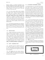
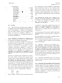
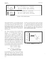
o
S«,IIIMJ..',ffO.
YOt<O!IIAWA �W1JlT II'4CII�flfl;'
0
'tOWl:1) J�
Figure 1-2.
Serial Number Plate
1-3
Section I
Model 4 I 92A
Table 1·1
Table '·1.
Specifications (Sheet 1 of 12)
COMMON SPECIFICATIONS
(Amplitude·Phase and Impedance Measurements)
INTERNAL SYNTH ESIZER:
Output from OSC OUTPUT (HCUR) terminal
Frequency Range:
5.000Hz to 1 3.000000MHz
Frequency Resolution:
I mHz (5Hz to 1 0kHz), I OmHz ( 1 0kHz t6 1 00kHz), 1 00mHz ( 1 00kHz to
I MHz), 1 Hz ( l MHz to 1 3 MHz)
Frequency Accuracy:
± 50 ppm (23'C ± 5'C)
OSC Level R .nge:
Variable from 5 mVrms to 1 . 1 Vrms (when terminated by s o n in amplitude
phase measurements or UNKNOWN terminals are open in impedance measure
ments).
OSC Level Resolution:
I mV ( 5 mV to 100mV), 5 mV ( l OOmV to 1 . 1 V)
OSC Level Accuracy:
OSC level
-----------
Measuring Frequency
,;;: lOOmV
> 100mV
5 Hz - I MHz
(5 + 10/f) % + 2 mV
(5 + I O/f)% + I O mV
I MHz - 1 3 MHz
(4 + 1 . 5F) % + 2 mV
(4 + 1 . 5F) % + I O mV
-
f : measuring frequency (Hz), F : measuring frequency (MHz).
Output Resistance:
son (amplitude/phase measurements), lOOn (impedance measurements, � 38kHz)
l OO n to 1 0 k" (impedance measurements, < 38 kHz, depends on measuring
range), dc coupling.
Level Monitor (impedance measurement):
Measures and displays the voltage across- or current through the
device under test.
Frequency and Level Control: Set via the front-panel numeric keys or HP-lB ; auto sweep (except for level) or
manual sweep.
E XT E RNAL SYNTHESIZER :
Connected to the VCO INPUT connector on the rear-panel (HP3325A Syn
thesizer or equivalent is recommended).
Frequency Range:
40,000005 MHz to 53 MHz (measuring frequency is equal to the frequency o f
the external synthesizer minus 40MHz [ 5 Hz to 1 3 MHz] ),
Required Signal level:
Note:
O dB m to 3 dB m
Frequency of the 4 192A internal synthesizer should be set to the frequency of the external synthesizer
minus 40Mflz, and the internal and external syn thesizers should be phase-locked,
1-4
Section I
Table ]·1
Model 4192A
Specifications (Sheet 2 o f 12)
Table 1 · 1 .
EXT R EF E R ENCE INPUT CONN E CTOR
Can be connected to a I MHz/ I O MHz high stability reference signal
(- I dBm to +5 dBm) to improve the stability of the internal synthesizer.
Approximately
Input Resistance:
son
MEASURING MODE:
Spot Measurement:
At specific frequency (or dc bias*)
Swept Measurement:
Between START and STOP frequencies (or dc bias*). Sweep can be automatic
or manual.
Linear sweep mode (sweeps at specified step) and logarithmic sweep mode (20
Sweep Mode:
measurement points per frequency decade).
Xl0 STEP:
Multiplies the specified frequency Idc bias* step by l O in linear manual sweeps.
PAUSE Key:
Temporarily stops swept measurements.
SWEEP ABORT Key:
Makes sweep cancellation.
* : DC bias sweeps can be made for impedance measurements only.
DC outputs proportional to measured values of D lSPLAY A. DlSPLAY B , and
RECORDER OUTPUT:
measuring frequency or de bias. PEN LIFT output and X-Y recorder scaling
outputs are provided.
Maximum Output:
±I V
Output Voltage Accuracy:
± (0. 5 % of output voltage + 20 mV).
FIVE NONVO LAT I L E STORAGE R EG ISTERS: Memorize five complete instrument measurement configurations.
Measurement configurations can be set from the front-panel, from the HP-lB,
or both.
Data output and remote control via the HP·IE (based on IEEE-Std-488 and
HP·IB INTER FACE:
ANSI·MC I · 1 .
I nterface Capabi l ity
:
Remote Control Function:
Data Output:
SHI , AH I , T5, L4, SR I , RLI , DC I , DTI .
All front-panel functions except LINE ON/OFF switch and X I O STEP key.
Measured values of D lSPLAY A, DISPLAY B, and measuring frequency or d e
bias.
S E L F TEST:
Performs the 41 92A basic operation checks and displays the test results when
power is turned on or when the SELF TEST mode is set by the SELF TEST key
or via HP-lB.
T R I G G E R:
Internal, External, Hold/Manual, or HP·lB remote control.
1-5
Section I
Table I - I
Model 4192A
Table 1 - 1 .
Specifications (Sheet 3 o f 12)
AMPLITUDE/PHASE M EASU R E M ENTS
PARAMETERS MEASURED:
Measures DISPLAY A parameters and D ISPLAY B parameters simultaneously in
the parameter combination listed below.
Deviation measurement (�) and
percent deviation measurement (,6,%) can be performed for all measurement
parameters.
DISPLAY A Function
DISPLAY B Function
Group delay (s)
B -- A (dB) : Amplitude ratio
1---
8 (deg/rad) : Phase Difference
-�,--
A (dBm/dBV) : Absolute amplitude of Reference Input
B (dBm/dBV) : Absolute amplitude of Test Input
R E F E R ENCE AMPLITUDE:
O dBv
=
I Vrms. OdBm
OSC OUTPUT CONNECTOR OUTPUT I M PEDANCE:
=
�
I mV (into SOn)
son + 5 % - 8 % (at 50Hz to 5MHz). s o n ± 10% (at 5 Hz to
1 3 MHz).
C H AN N E L A AND B :
Input Impedance:
I M n ± 2%, shunt capacitance 25 pF ± 5pF
Maximum Input Voltage:
2 Vrms/± 3 5 V DC Max.
D ISPLAY RANGE AND RESOLUTION:
In NORMAL or AVERAGE measurement mode (Measuring resolution de-
creases one digit in HIGH SPEED measurement mode.
B
-
A:
0 to ± 1 0 0dB, O . O O l dB (0 - 2 0dB), O . O l dB (20 - I OOdB) resolution
e:
0 to ± 1 80 ' (0 to ±
Group Delay (7g):
O. lns to 1 9 .9998, O . l ns maximum resolution
A, B:
+0.8dBV to - I OO dBV, + 1 3 . 8 dBm to - 87 dBm, O.OO l dB (> - 20dB), O.O l dB (:;:; - 20 dB)
resolution
1-6
7
radian), 0.0 1 ' resolution
Section I
Table I-I
Model 4192A
Table 1 - 1 .
Specifications (Sheet 4 o f 12)
Specified at measuring terminals when the following conditions are satisfied :
M EASU R I N G ACCURACY:
( 1 ) Warmup Time:
> 30 minutes
(2) Ambient Temperature:
23°C ± S O C (error limits double for O°C to S S OC temperature range).
(3) Measuring Speed:
NORMAL or AVERAGE mode.
Note:
A dditional errors due to the power splitter, feedthrough termination, etc" are to be added to speci/i
cations given here.
The measurement accuracy of each parameter is given below. The accuracy depends on input absolute level of
each channel and the measuring frequency.
8-A and
e
Measurements Accuracies :
Accuracies are the sum of each channel accuracy given in the table
below. For example, when the frequency is 1 kHz, A channel is - I S dBV and B
channel is - 25 dBV ; the uncertainty contributed by each channel to the B -A
error is 0.01 dB/O.OSo and 0.05 dB/O. I S o, respectively. Therefore, the final ac
curacy of 0.06dB/0.2° is given by the accuracy of both channels.
Accuracy is derived from the following equation (phase accuracy LeA
Group Delay Measurements Accuracy:
and
LeE
are read from the table below):
group delay accuracy
Channel A phase accuracy (degree)
Channel B phase accuracy (degree)
Step Frequency (Hz)
�
>
'"
+0.8
'0
-10
c
c
�
-20
�
"
0
-'"
u
"
'"
""'
0
"
>
v
....l
'"
;;
'0
�
-"
�
-
�
0.
c
-
f :
(0.008+0.2/fldB
(0.04+1/flo
O.OldS
0.05°
0.045dS
0.08°
(0.025+0.02FldS
0.08Fo
(0.047+0.2/f)dS
(0.13+2/flo
0.05dS
0.15°
0.08dS
0.25°
(0.04+0.04F)dS
(0.05+0.2Flo
(0.05+1/fldB
(0.14+6/flo
0.06dB
0.2°
0.12dB
0.3°
(0.06+0.06F)dB
(0.05+0.25F)0
(0.05+3/fldB
(0.15+15/flo
0.08dS
0.3°
0.14dB
0.6°
(0.07+0.07F)dB
(0.3+0.3F)O
F : measuring frequency (MHz)
Equations in table represent:
-30
-40
-50
-60
-70
-80
(O.l+lO/f)dB
(1+50/f)0
0.2dS
1.5°
(O.l+O.lF)dB
(1+0.5F)0
(0.45+25/fldB
(4+100/f)0
0.7d8
5°
(0.4+0.3FldB
(4+F)0
(1.5+50/f)dB
(12+300/f)0
2dS
1 5°
A, B accuracy
() accuracy
Note
W hen calculating accuracy
for points along a horizontal
or vertical line, or at the
intersection of two lines, use
narrowest
accuracy
the
equation.
(1+FldB
(13+2F)0
Unspecified
-90
-100
measuring frequency (Hz)
5
100
10k
lM
l3M
Measuring Frequency (Hz)
1 -7
Section I
Table 1·1
Model 4192A
Table '·1.
Specifications (Sheet 5 of 12)
Absolute Amplitude (A, B) Accuracy: Accuracy is given in the table below,
:>
00
"0
�
Q
"
"
"
""
U
"'
u
"
�
+O.S
-10
f
measuring frequency (Hz)
F:
measuring frequency (MHz)
-20
(0.4+1/f)dB
0,4dB
(0.4+0.0SF}dB
-30
Note
4-<
0
"il
-40
>
-50
(3
-60
W hen calculating accuracy
for points along a horizontal
or vert ical l ine, or at the
intersection of two lines, use
the
narrowest
accuracy
equation.
"
..-l
"
"
�
.re
<
"
'"
.s
(0.5+11/f)dB
0.6dB
(0.5+0.1SF)dB
(0.85+26/f)dB
1.1dB
(0.8+0.38F)dB
(1.9+51/f}dB
2.4dB
(1.4+1.08F}dB
-70
-SO
5,;;
100<
�100
Unspecified
-90
-100
5
100
,
lM
Measuring Frequency (Hz)
1-8
l3M
Model 4192A
Section I
Table 1·1
Specifications (Sheet 6 of 12)
Table 1·1.
IMPEDANCE MEASUREM ENTS
Measures DISPLAY A parameters and DISPLAY B parameters simultaneously in
PARAMETERS MEASU R E D:
the parameter combinations listed below, Deviation measurement (.6.) and
percent deviation measurement (.6%) can be performed for all measurement
parameters.
D I SPLAY A Function
IZI
IYI
Absolute Value of Impedance
:
Absolute Value of Admittance
Resistance
G
Conductance
C
e (deg/rad) : Phase Angle
----�---
R
L
DISPLAY B F u nction
X
._-
B
-------
:
Capacitance
EQUIVALENT C I RC U I T M O D E:
Auto, � (Series), and
o-CJ-'NrO
D I SPLAY:
�
mode; and I Y I , G, and B in
Reactance
Susceptance
---
-
Q
Quality Factor
D
Dissipation Factor
R
Resistance
G
Conductance
--
Inductance
:
--
(Parallel)_ I Z I , R, and X are measured in
�
mode.
Maximum 4 ' 1 / 2 digits in N ORMAL or AVERAGE measurement m ode,
maximum 3 ' 1 / 2 digits in HIGH SPEED m easurement m ode; 1 9999
full-scale display for L and C m easurement, 1 2999 for other parameters.
Number of display digits depends on OSC level, measurement range, and
test frequency. (Refer t o Para. 3-17)
RANGING:
AUTO or MANUAL for impedance ( I Z I )/admittance ( I Y I ) measured value.
MEASUREMENT T E R M I N A L:
4-terminal pair configuration
AUTOMATIC ZERO ADJUSTMENT:
Residual impedance (R + jX) and stray admittance (G + jB) of the test fixture
are measured at a frequency selected by the operator. These values are then
stored and used as offset data for subsequent measurements. The stored offset
values are converted and applied to other measurement frequencies (refer to
paragraph 3-79).
1-9
Model 4192A
Section I
Table I-I
Specifications (Sheet 7 of 12)
Table 1-1.
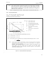
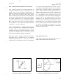
M EASU R I NG RANG E AND R ESOLUTION:
Accuracy is specified at UNKNOWN terminals under the following
conditions:
� 30 minutes
(1)
Warmup Time :
(2)
In Floating Measurements:
(3)
Measuring Frequency:
At the frequency of the zero offset adjustment
(4)
Ambient Temperature:
23°C ± 5°C (error limits double for temperature range of oOe to 55°C)
(5) CABLE LENGTH:
(6)
Measuring Speed:
(7)
In the tables,
(see Table 1 -2 for specifics on low-grounded measurements)
At 0 position
NORMAL or AVERAGE mode
area: Reference data (accuracy is not guaranteed.)
� area : Measurement can not mode but accuracy is not specified.
1 00>lg -1 80.000 to + 1 80.000
0.0001 to 1 . 2999M>l
0 02
+ . : use the Icft graph (below)
B =
'I
e =
'I
: use the right graph (below)
where 'Y
ose LEVEL (V)
f : Measuring frequency (Hz)
F : Measuring frequency (MHz)
200
5
100
10
2
OL-�________�________77
1.1
5m lam
1 Dam
DSC
1 -1 0
LEVEL(V)
lOOm
5m 10m
DSC
LEVEL(V)
1.1
Model 4192A
Section I
Table I-I
Table 1-1.
Specifications (Sheet 8 of 12)
IZI-8 and R-X Measurements:
Measuring Range:
Maximum Resolution
Parameter
Measuring Range
IZI· R ' X
0.000] n to 1.2999Mn
8
- 180. 00° to +180.00°
1------+--- -----------1- ----------1
Measurement Accuracy :
Refer to the table below (specified by ZY RANGE). However, R and X ac
curacy depends on the value of D as follows:
1 � D < 10
D < 1
10�D
!
Table
Accuracy of R is equal to the accuracy of
Two times % error given in the table below.
below
X, in number of counts, as calculated from
R
tbe table below.
1-----+---- ---------1----- ------------L
--j
_ __ ___
X
Accuracy of X is equal to the accuracy of R, in
number of counts, as calculated from the table be
low.
Table below.
{(C.2 +A)B+f (1 t 2.4A·O] %+1
+0.5A)8+,� (1 +2.4A.C)}o
[(0.1 +0.2A)8+lil +0.03 (1 +lOA)c}]%+ 1
lOOk
1:(0.05 + 0.lA)8 t t{1 +0.03 (1 +lOA)c}]"
(1 +10A)C}]%+ I
10k [(0.1 +O.2A)B+t{1..-0.02
'
[(0.05 0.1A)8 t tt1 +0.02 (1 +10A)c}]�
lM
(O.ZF +A)8%+1
(O.12F +0.5A)8°
(0.2 + A}B%+1
(0.1 +0.5A)8°
{CG.l
(G.2f 0.2A)8%1 1
(0.12F t 0.1A)BO
t
'
(0.1 ;. 0.2Al8%;.
(O.OS ;. O.lAW·
+
I
(0.15F '" 0.2AJtH.;.
{ O . 09F"' O.lA)BO
[(0.1 +0.2Al8-;- t {l +0.04 (1 .;. 6A. )C}]%;. 1
[(0.05 +O.lA)8 � {l ",0.04 (1 +6Ale}]0
0.13'%+3
(0.1 '" 0.02F ... 0.OZ4F')B%+3
(0.05 + °A01)BO
(0.05 +9..:%l +O.OlF +0.014f")B'(
0.26%+5
(0.2" 0.03F ,. 0.032F')B%., 5
(0.1 .. °iliJIw (0.1 +Q. ,.jF ·.0.06F +0.064Fl}(0.2+2.p;.1.)BC
0.58% ." 5
(0.3 +;�}BO
100
10
1
(0.1 + 0.2A -;- 0.02F +0.024F2jB;{ +1
(0.05 +O.lA +O.OiF +0.014F2)B6
.j.
N
__
[0.28+t { 1 +0.04 (1 +i.!c} J% -I- 5
[(0.1 +·4.£)13 +i {1 +0.04 (1 +�")c} JO
,
400
IM
1M
13�\
Measuring Frequency (Hz)
(1)
Displayed
IZI, R or X (n )
-A 121 Range full scale (n )
(2)
Equations in table represent :
in the table.
I ZI, R, X accuracy [ ± (% of reading + number of counts) 1
8 accuracy [ ± (absolute value)]
1-11
Section I
Table 1-1
Model 4192A
Table 1-1.
IYI
-
0
Specifications (Sheet 9 of 12)
and G- B Measurements :
Measuring Range :
Parameter
Measuring Range
Maximum Resolution
0 00I S� _
_ 12_ .9
_9
_ 9S
_ __
_+--- ---+-� .� � �M�
- 1 80.00° + 1 80.00'
IY
r-____
_ _ I,_ �, B:
______
e
lnS------
Refer to the table below (specified by ZY RANGE). However, G and B accuracy
Measurement Accuracy:
depends on the value of D as follows:
D :;:; 0.1
G
0.1 < D :;:; 1
Two times % error given in
the table below.
Table below
{( O. 1
+
V1
�
"
'"
�
'"
�
><
l Om
[0.18+t{l
t
[0.18+if1
0.2B%+ 3
O.2H�%+ 3
{G.l+ 2..:
(0.12f" +Q�*
t'
+
5_)BO
O.2F -B" + 3
3
}
(O.12F
+
3
0.04 {l+
0;i,6)C}]% +
+
0.04
ifl
+
(1
c
9"%lw
.;-
�
Q_·,. J)BQ
{O.l + 0.02F + 0.024Fl)B% +3
+ Q.,'£l + O.OlF+0.014FlW
3
(O.OS
(0.1.;. O.2AlB%' 1
(0.05+O.lA)SC
,i,
'e
(0.09t
°A5)C} ]0
0.2A)B+
[(0.05+ O.lA)B+ { 1
..
O.15F·B%+3
0.18%+3
{O.05 +9f)BO
} }]O
(1 + )c
f' {1+0.04 (1 + 2A)C}]%+1
0.04 (1 +2A)C} JO
t
[(0.2+O.SA)B " f { 1 +0.04 ('I +20A)C}]%+1
[(0.1+0.2A)S + f {1 0.04 (1+ 20A)C} JO
f----b
1DOm
[(0.1
'f.
{ C } ]% +
0.02 (1+ )
[(0.05+Q'iiQ.l')B+tt 1 + 0.02
[(0.05
Accuracy of B is equal to the accuracy of G, in
number of counts, as calculated from the table
below.
--{1+O.03(1+ }C}Jo
[O.OS-!
"
Table below
-£2)B�
0.03 (1+ k)C}]%
100), [O.lS + t{l +
1
�
1 < D
Accuracy of G is equal to the accuracy of S, in
number of counts, as calculated from tbe table
below.
B
(0.2 '. o.SAlB%+
(0.1
+ O.2A)8Q
(C.5 +2AiBl
(0.3 " A}!l%
400
"
(0.1+O.2A + O.02F + 0.024F')B% + 1
{0.05 + O.l A+O.01F + 0.014F2)BO
1
1
16k
13M
Measuring Frequency (Hz)
(I) A =
Displayed IYI, G or B (S)
IYI Range full scale (S)
in the table.
( 2 ) Equations in table represent :
IYI, G, B accuracy: [ ± (% o f reading
e
1- 1 2
�
accuracy:[ ± (absolute value)]
+ number of counts)]
Section I
Table 1·1
Model 4192A
Table 1-1.
Specifi cati ons (Sheet 10 of 12)
Refer to R/X or G/B measurements for R and G accuracy.
L-Q, D, R, G Measurements:
Measuring Range:
Parameter
M easuring Range
L*
0.0] nH
D
0.0001
_.._----
Q
*
0.1
-
M ax imum Resolution
! OpH
1 .0000kl-l
-
-
"---
1 9.999
0.0001
1 999.9
0. 1
Depends on ZY RANGE and measuring frequency (refer to paragraph 3-71).
Refer to the table below (specified by ZY RANGE).
Measuring Accuracy :
To determine which IZ I range is selected for L measurements,
change the DISPLAY A function to 1 Z lilY I.
1+ 2A)8
1M
lOOk
10k
1k
lOG
;-
t {l
(0.01 + 0.02A)8 +
[(0.2
,I,
O.3f,)S
t
+
t { 1+ 0.03 (1+ 10A)C}]% t 1
{l + 0.03 (1
i {1+ 0.002
(0.002+ 0.003A)8
[(0.2
(0.002
+
0.3A)8 +
+
(0.01 + Q,02A}tl
(l+ 2,4A·C)
(0.002 ., 0.003A)8 +
[(0.2+ 0.3A)8
(l ;- 2AW:· t !
Z.4A·C)r %+ 1
9fQ·�
+
+
(O.3F+ O.3A)BX -;- 1
0.0031"+ 0.003A)B
lOA)C}
(1+ WA)cf]%+ 1
(0.2
O O
- S
f {l+ 0.03 (1 -;- lOA)C}
�,{ 1
-I-
0.04 (1
{
+
}
O.3A)ln
+
1
(O.2f + 0.3A)8%+ 1
+
-I-
(O.002f
6 Ale} ]%+ 1
1+ 0.02 (1
[0.2B+
!,
(0.002 '0.003A)B
0.003AlB
+ 0.3A+ 0.03F
�
0.032f2)S% + 1
I, 0.003A + 0.0003F + 0.0004F'lB
10A)c}
J:ti3
0.2B'r+ 3
(0.2 + 0.031" + 0.032eW�" 3
(0.002"
O.3BX.+ 5
(0.3 + 0.04F+ 0.048F2)S1. + 5
2.,_9.£93.)8
�1---�'-��----�--+---�--*=
0.78% + 5
10
+ 0.0003F + O.0004F')S
+ 0.0004F
(0.003 +
�
0.0006F2)B
�
02
{O.OO? + fL... )B
400
1M
16k
BM
1M
Measuring Frequency (Hz)
(I) A =
2n X Measuring frequency (Hz) X Displayed L (H)
I Z I Range full scale (H)
in the table.
(2) Equations in table represent (at D � 0. 1 ) :
L accuracy: [ ± (% of reading + number of counts)]
D aceuracy :[ ± (absolute value)]
(3) If 0. 1 < D � I , double the % error for all values of L.
(4) If D > 0. 1 , multiply error of D by ( l + D)' .
(5) a= 2nf
Where f3
5
x
le.
IOs(H) in the tab
number o f digits displayed when the DISPLAY A function is
changed to. t Z I / 1 Y 1
•
1-13
Section I
Table I-I
Model 4192A
Specifications (Sheet 1 1 o f 12)
Table 1 - 1 .
C-Q, 0, R, G Measurments:
Refer to R/X or G/B measurements for R and G accuracy.
Measuring Range:
Parameter
'---'-' -'
* .
Measurement Range
C*
O.OOOlpF
-
100.00mF
O. l f F
D
0.0001
-
1 9.999
0.0001
Q
0. 1
-
1 999.9
0. 1
Refer to the table below (specified by ZY RANGE).
To determine which I Z I range is selected for L measurements,
change the DISPLA Y A function to I Z I I I Y I .
O.2F ·5% + 3
.9�,�Ql)B
0.213% 3
(0.002 + Q·�01�)B
4-
(O.OOZF
f
�
@
0:::
;><
lrn
___
[O.lB + � { 1 4- 0.02
(0.0009 +
(1;.
})c} Ji 3
{l + 0.04 (1 + 0 flC}
O.lB% + 3
(0.0009 + O.�D91_)S
t
r-�,---��----��,-----�--�
} ]% + 3
lOin
(0.0009 +
lOOm
!-
(0.002;. 0.004A)B;.
Jf
(0.1 + 0.2A)B% + 1
(0.0009 + 2.:..0 �02)B
0.04 (1 ;. 20A)c}]% + 1
{1 + 0.04 (1 ;. 20A)C}
(0.2 ;. 0.5A)B% ,. 1
(0.002 ;. 0.004A)8
{l
"
2A)C}
+
1
O. i5F·BX. ;. 3
(O.0016f .. Q.,O�OZ)B
r-,---------�------�
(0.1 + O.02F + O.024F2)8% + 3
(0.0009 + O.O�02 + O.0002F + O.0003F2)B
{1 + 0.04 (1 ",2A)c}
(0.0009 ;.
+
G.2F·B% + 3
(O.002F + Q�.Qo.?-)B
[O.lB +t{l + 0,03 (1 A:)C}
(0.0009 O �002)B + �Q.�,{ 1 + 0.03 (1 ,. k)C}
§
-
Depenction ZY RANGE and measuring frequency (refer to paragraph 3-7 1 ).
Measurement Accuracy :
'e
M ax imum Resolution
(0.1 + 0.2A + 0.02F + 0.024F1i8% ., 1
(0.1:\009 + Q.,�..QQS 0.0002F O.0003F1)B
-I-
t
(0.5 + 2Aj-B% + I
(0.005 + q.02A)B-
10
400
16k
IM
2M
13M
Measuring Frequency (Hz)
(1) A
=
2 rr X Measuring frequency (Hz) X Displayed C (F)
lyrRange ' full scale
( 2 ) Equations in table represent (at D � 0 . 1 ) :
C accuracy:[ ± (% of reading + number of counts)]
D accuracy:[ ± (absolute value)]
(3) If 0. 1 < D � 1 , double the % error for all values of C.
(4) If D > 0. 1 , multiply error o f D by ( l + D)' .
(5)
a=
211f
3
x
la S+
,(F) in
the table.
Where f3 : number of digits displayed when the DISPLAY A function is
changed to I Z I / I Y I .
1-14
Section I
Table 1 ·1
Model 4192A
Table '·1.
Specifications (Sheet 12 of 12)
Valid for impedance measurements only.
DC BIAS:
Voltage Range:
-35 V to +3 5 V , l O mV steps
'
Setting Accuracy (at 23' C ± 5 C ) :
± (0.5 % of setting +5 mY)
Output Resistance:
liOn to 1 1 kn ± 1 0 % (depends on measuring range)
Max imum Output Current:
Varies with measuring frequency and range,
- 20mA max.
Low-grounded measurements - 5 mA max.
Floating measurements
Control:
Front-panel numeric keys or HP-IB remote control
G E NERAL
OPERAT I N G T E M PE R AT U R E :
O'C to 5 5 ° C
R E L AT IV E HUM I D ITY:
� 95% at 40° C
POWER:
1 00, 1 20, 220 V ± 1 0%, 240V + 5 % - 1 0%, 48Hz to 66Hz, power consumption
150 VA maximum.
D I M EN S IONS:
425 . 5 mm (W) X 235 mm (H) X 6 1 5 mm (D)
WEIGHT:
Approximately 19 kg
F UR N I SH E D ACCESSO R I ES AND PARTS :
1 6047A Test Fixture, 1 1 048C 50n Feedthrough Termination (2 ea.),
Splitter (HP Part N o . : 0 4 1 92-6 1 0 0 1 , Nominal 50n ) , Power Cord (HP Part No. :
8 1 20- 1 378).
OPTIONS
OPT IO N 907:
Front Handle Kit (HP Part No.: 506 1 -009 1 )
OPT IO N 908 :
Rack Flange Kit (HP Part No. : 506 1 -0079)
OPT I O N 909:
Rack and Handle Kit (HP Part No. : 506 1-0085)
OPTION 910:
Extra Manual
1-15
Section [
Table 1 ·2
Model 4 1 9 2A
General I nformation (Sheet 1 of 2)
Table 1·2.
G E N E R A L I N FO RMATION
(The following information is reference data and not guara nteed specifications.)
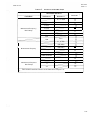
TYPICAL M E AS U R E M E NT ACCURACY :
Impedance Measurement ( F loating) :
Accuracy when CABLE LENGTH is I m : 2.5 times percent error for frequencies above I MHz.
L . C accuracy for D > I : ( 1 + D 2 ) times accuracy specifications
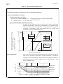
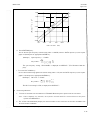
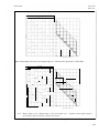
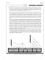
Low Grounded Impedance Measurement Accuracy :
To obtain low grounded measurement accuracy, add the accuracy for floating
impedance measurements, given in the proceding tables, to the additional error
given in the figure below. Compensation for residual impedance (;;; 9pF at
;s;: 600kHz or approximately 20kn at � 600kHz) must also be made using
the 4 1 92A's zero offset adjustment function.
10
�
on
---
.S
'"
-0
�
4-0
0
�
�
DSC
LEVEL
"
�
en
"
�
�
l
N
::s
»
Range
I�/
1.0
"
§ ""'
" �
"
.§ " 0"
�
:0
u
.9 �
-< - en
:0 "
-0
� -0
-<
:::- ""
N �
0
I lY
;OOkQ,lMn
>70mV !100\l$,10;J5
<70rnV lDkQ,lmS
'0)
0
� Q
�
�
iZ i "
,-,•
.;:;
"
�
'"
"'
;:;:
0.1
5
-1
l OK
/
/
/
/
/
/
/,
/,
/
/
/
7
/
l OOK
/,
/'
/,
/'
..-
/'
/'
/'
..-
/'
,-
--
--
------DSC
ZY Ranqe
LEVEL
) 70mV 1Okn, lmS
frv kn
<;.70mV
10mS'\..10S
�
,-
/"
....
J-------
--
DSC
LEVEL
ZY Range
>70mV
l�lkQ
1OmSo.,lOS
'-
--- --
l OM
lM
Measuring Frequency (Hz)
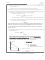
Refer to the figure below (at fixed measuring frequency) measurement range and
MEAS U R I N G SPEED :
OSC level for impedance measurement). Specific information is provided in
paragraph 3-55 for amplitude/phase measurements and in paragraph 3-89 for im
pedance measurements. Speed in AVERAGE mode is approximately 7 times
that for NORMAL mode.
:3
3.
_�====�==����=
�
0
§
f-<
C
300m
�
�
lOOm
v
E
v
0
:2i
30m
High Speed
:===j==\[=::t====�====� Nonnal Speed
High Speed
5
10
100
lK
lOOK
Measuring Frequency (Hz)
1-16
Nonnal Speed
lM
l3M
Model 4 1 9 2A
Section I
Table 1-2
Table 1-2.
General I nformation (Sheet 2 of 2)
F R EQ U E NCY SW ITCHING T I M E :
Approximately 50ms to 65ms
ZY RANGE SWITC H I NG T I M E :
Approximately 35ms to 50ms per range (at> 400Hz)
OSC L EV E L SWITC H I NG T I M E :
Approximately 65ms
DC B I AS VOLTAGE SETT L I NG T I M E :
Approximately ( 0.4 X I'N + 1 0) ms where DV is the v oltage change (V) .
L EV E L MONITOR RANGE AND ACCURACY :
�
Voltage
C urrent
At 23°C
±
5°C
5mV
I}.(A
�
T I M E R EQ U I R E D FOR LEVE L MONITOR :
Output Resistance :
,;;; 1 00Hz: (4 + 1 0/f ) % + I
1 00Hz to IMHz : 4% + I
� IMHz : (4 + O. SF) % + I
l.l V
�
where f: measuring frequency (Hz),
1 M H z R E F E R E NC E OUTPUT :
Accu racy (% of reading + count)
Range
F
:
measuring frequen cy ( MHz).
Approx imately 1 20ms
Square wave, L 1 .6 Vp-p
Approximat ely son
1-17
Section I
Paragraphs 1 ·22 to 1·29
'·22.
Model 4 192A
OPTIONS
Option 910 adds an extra copy of the Operation
and Service Manual.
1-25.
Options are modifi cations to the standard instru
ment that implement the user's special requirements for
minor f un ctional changes. The 4192 A has f our options
as listed in Table 1·3.
1-23.
Tab le '·3
Option
Number
Available O ptions
'·26.
The HP Model 4192A LF Impedance Analyzer,
along with its furnished accessories, is shown in Figure
I - I . The f urnished accessories are also listed below.
1-27.
16047 A
l 1 048C
Description
907
Front Handle Kit.
908
Rack Flange Kit.
909
Rack Flange and Front Handle Kit .
910
Extra Manual
ACCESSOR I ES SUPPL I E D
'·28.
Test Fixture
s o n Feedthrough (2 ea.)
Power Splitter (HP Part No.: 0 4 1 92-61 00 1 )
BNC Adapter (HP Part No.: 1250-0216)
11170A
BNC Cable (2 ea.)
Power Cable
(HP Part No.: 8 120-1378)
Additional Fuses f or AlP! (2ea . P N: 2 1 1 0-0650)
ACCESSO R I ES AVAI LAB L E
For certain measurements and f or convenien ce in
connecting samples, ten types of accessories are available.
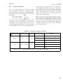
Each accessory is designed to meet the v arious measure
ment requirements and types of DUT. All accessories
were developed with careful consideration to accuracy
reliability, and ease of measurement. A brief description
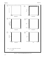
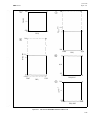
and p hoto of each available accessory is given in Table
1-29.
The following options provide the mechanical
parts necessary for rack mounting and hand carrying:
1-24.
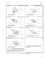
Option 907 : Front Handle Kit. Furnishes carrying
han dles for both ends of f ront-panel.
Option 908 : Rack Flange Kit. Furnishes flanges for rack
mounting for both ends of front-panel.
Option
909 :
Rack Flange and Front Handle Kit. Fur
n ishes both f ront handles and rack flanges
f or in strument.
Installation procedures for these option s are detailed in
Section IT.
1-18
J
1-4.
Model 4 l 92A
Section I
Table 1-4
Table 1-4.
Model
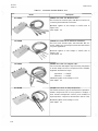
HP 1 6047A
Accessories Available (Sheet 1 of 4)
Description
1 6047A Direct Coupled Test F ix ture (furnished ) :
Test Fixtur e (direct attachment type) for general measur e
ment of both ax ial and radial l ead component s. Three
kinds of contact inserts are f urnished:
CD For axial lead components,
(HP PIN 16061-70022).
(3) For general radial lead components,
(HP PIN 16061-70021).
o For radial short lead components,
( HP PIN 1 6047-65 0 0 1 ).
DC bias up to ±35V can be applied.
H P 1 6047B
1 6047B Test Fix ture with Safe Guard:
Test Fixt ur e (cable connect ion type) for general measure
ment of both ax ial an d radial lead components at fr e
quen cies below 2 MHz. Three kinds of contact inserts are
furnished (same as those for the 16047A Test Fixture).
DC bias up to ±35V can b e applied with using the 4192A
(a protective cover provides f or operator safety).
Cable length: approximately 40 cm
HP 1 6 047C
1 6047C High Frequency Test F ix ture:
Test Fixture (direct attachment type) especially appro
priat e for high frequen cy measurements requiring high
accuracy. Two screw knobs f acilitate and ensure optimum
contact of electrodes and sample leads. Maximum appl ied
de bias voltage is ±35V.
1-19
Section I
Table 1 - 4
Model 4 192A
Table 1-4.
Accessories Available (Sheet 2 of 4)
Model
HP 16048A
Descri pti on
16048A Test Leads with B N C Connector:
Test Leads (four tenuinal pair) with BNC connectors for
connecting user-fabricated test fixtures.
Maximum applied de bias voltage is ±200V (refer to
Figure 3-34).
C able length: Im
HP 16048B
16048B Test Leads with R F Miniature Connectors:
Test Lead ( four terminal pair) with miniature RF con
nectors suitable for connecting user-fabricated test fixtures
in systems applications.
Maximum applied dc bias voltage is ±200V (refer to
Figure 3-34).
C able length: l m
HP 16048C
16048C Tes t Leads with Alli gator Cil ps:
Test Leads with dual alligator clips for testing components
of various shapes and sizes at frequencies below 1 00kHz.
Applicable measurement ranges:
Capacitance > 1 000p F
Inductance > 1 00 J.LH
Maximum applied dc bias voltage is ±3SV.
C able length: I m
HP 16034B
16034B Test F x
i ture for Chip Components:
Test Fixture (tweezer type) for measurement of miniature,
leadless components such as chip capacitors. Employs a
three terminal configuration tweezer probe suitable for
high impedance component measurements (above SOn).
Maximum applied de b ias voltage is ±3SV.
C able length: I
In
1-20
Section I
Table 1 4
Mode1 4 1 9 2A
Table 1-4.
Acce ssories Available (Sheet 3 of 4)
Description
Model
HP 16095A
HP 16095A Probe F ix ture:
For probe impedance measurements on board-mounted
components or entire circuits. Low lead can be floated or
grounded. OSC OUTPUT connect or is provided for am
plitude-phase measurements. Following data is specified
when BNC a da pter is used:
Stray capa citan ce
� ISpF
Residual in ductan ce: � 40nH
Residual resistance : � JOOm n
Following parts are furnished.
Part
Center pins for probe ( 1 0 ea .)
Alligator clip for ground
BNC (mal e) ada pter
Alligator clip adapter
HP Part N o.
16095-600 1 2
16095-6 1 6 1 1
16095-600 1 1
16095-6 16 1 2
Groun d pin s (5 ea., HP Part No. 1 6095-65001 ) are also
available (not furnished).
16097A
16097A Accessory Kit (with carrying case ):
Contain s the following accessories for circuit measurements:
1 1 094B
1 1095A
1 1 070B
1 1 170C
1 00 1 3A
1 0007B
16047C
1 6048C
1 6095A
75n Feedthrough (2 ea .)
600n Feedthrough (2 ea.)
60cm BNC cable (2 ea.)
1 20cm BNC cable (2 ea .)
1 0 : 1 Scope probe (2 ea. )
1 : 1 Scope probe (2 ea.)
Test Fixture
Test Leads
Probe Fixture
1-2 1
Section I
Table 1·4
Mode1 4 l92A
Table 1-4.
Accessories Available (Sheet 4 of 4)
Description
Model
16096A
16096A Test Fix ture:
To alternately make amplitude/phase measurements and
input i mpedance measurements on two-port devices. Fol
lowing data is specified at BNC connectors:
Residual Impedan ces (after zero offset adjustment):
Stray capacitance
� O.O l pF
Residual Inductance: :s;;: ( lOO + 0.5F')nH
Residual resistan ce � (50 + 5F') m.l"l
:
Error in amplitude/phase measurements (aft er cable com
pensation) :
B·-A error : ±O. l dB
Phase error: ±O.lo
A, B error : ± (0.1 + 0.06F') dB
Input i mpedance of CHANNEL A/B :
less than 1 5pF.
I M.I"l
shunted by
Following parts are furnished:
Part
Textool® Grid zip test socket kit
H P Part No.
1 6 096-6500 I
16096-6 1 6 1 4
BNC (male) to dual alligator clip cable
(4 ea.)
16096-6 1 6 1 1
BNC (male) to SMC cable
(4 ea.)
16096-6 1 6 1 3
Banana plug to alligator clip cable
BNC (male) - BNC (male) cable
16096-6 1 6 1 5
(90cm)
BNC T adapt er
1 250-078 1
1-22
Section II
Paragraphs 2-1 to 2-9
Model 4192A
SECTION 1 1
INSTALLATION
2·1.
2-2. This section provides installation instr uctions for
the Model 4 1 92A Impedance An alyzer. The section al so
in cl udes inf ormation on initial in spection and damage
claims, preparation for using the 4 1 92A , packaging,
storage, an d shipment.
2·3.
I N ITIAL INSPECTION
2·4. The 4 192A Impedance Analyzer , as shipped from
the factory, meets all the specification s listed in Tabl e
I -I. Upon r eceipt, inspect the shipping container for
damage. If the shipping container or cushion ing material
is damaged, it should be kept until the contents of the
shipment have been checked for completeness and the in
strument has been checked mechanicall y and electrically.
The contents of the shipment should be as shown in
Figure H . The pr ocedures for checking electrical per
f or mance are given in Section rn, paragraph 3-7, Self Test
and in Section IV, Performance Tests. If the shipment is
incomplete, if the in strument is damaged in any way, or
if the instr ument does n ot pass the Perfor mance Tests,
n otify the nearest Hewlett-Packard off i ce. If the shipping
container is damaged, n otify the carrier as well asHewlett
Packard. K eep the shipping materials f or the carrier's
inspection . The HP office will arrange for repair or re
placement without waiting for claim settlement.
2-5.
P R E PARATION FOR USE
2·6.
Power Requirements
The 4 1 92A requires a power source of 1 00, 1 20,
220 Volts ac ± I O%, or 240 Volts ac + 5 % - 1 0%, 48 to
6 6Hz single phase; power consumption is 1 50 VA maxi
mum.
2-7.
WARNING
INTRODUCTION
THIS IS A SAFETY CLASS I PRODUCT (PRO
VIDED WITH A PROTECTIVE EARTH TERMI
NAL). AN UNINTERRUPTlBLE SAFETY EARTH
GROUND MUST BE PROVIDED FROM THE MAIN
POWER SOURCE TO THE INSTRUMENT'S IN
PUT WIRING TERMINALS, POWER CORD, OR
SUPPLIED POWER CORD SET. WHENEVER THE
SAFETY EARTH GROUND H A S BEEN IM
PAIRED, TH E INSTRUMENT MUST BE MADE
INOPERATIVE AND BE SECURED AGAINST
ANY UNINTENDED OPERATION. IF THIS IN
STRUMENT IS TO BE ENERGIZED VIA AN
AUTOTRANSFORMER FOR VOLTAGE REDUC
TION, MAKE SURE THAT THE COMMON TER
MINAL IS CONNECTED TO THE EARTH POLE
OF THE POWER SOURCE.
2-8.
Line Voltage and Fuse Selection
CAUTION
BEFORE CONNECTING THE INSTRUMENT TO THE
POWER SOURCE, make sure that the correct fuse has
been installed and that the line voltage selection switch
is set to the correct voltage.
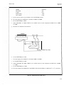
2-9. Figure 2-1 provides instructions for line voltage
and fuse sel ection . The line voltage sel ection switch and
the pr oper fuse are f actory in stalled for 1 00 or 1 20 volts
ac operation . Current ratings for the fuse are printed
under the fusehol der on the instrument's r ear-panel and
are listed, with HP part numbers, in Figure 2-1 .
CAUTION
Use the pr oper fuse for the line voltage selected. Make
sure that only fuses for the required rated current and of
the specified type are used for replacement. The use of
mended fuses or short-circuited fuse-holders must be
avoided.
Section II
Paragraphs 2· 1 0 to 2 · 1 5
Model 4192A
Line Voltage Selection
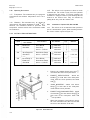
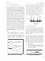
r-----
�
L I N E ----,
VOLTAGE
SELECTOR
�
FUSE
J
ixi=::::: ili
1 �
100V�
j,25AT
�
OO AT
250V'"
240V'"
Figure 2·1.
2-10.
POWER CABLE
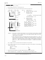
Use a screwdriver to set the Lin e Voltage Sel ector
switch to the appropriate voltage,
Fuse Removal
Using a screwdriver, turn the f use holder CCW45' or
until it pops-out of the fuse socket,
Line Voltage
I OOV/120V
220V/240V
Fuse Rating
l .25AT, 250V,
Slow Blow
0,6AT, 250V,
Sl ow Bl ow
HP Part No,
---
2 1 10 - 0305
2 1 10 - 0016
Line Voltage and Fuse Selection.
needed for selecting the correct power cabl e, contact the
nearest Hewlett-Packard office,
2-11, To prot ect operating personnel , the National
Electrical Manufacturer's Association (NEMA) recom 2·14. Interconnections
mends that the instrument panel and cabin et be grounded.
The Model 4 192A is equipped with a three-conductor 2-15, To interconnect the 4192A to an extern al con
power cabl e which, when plugged into an app ropriate ac troller or peripheral device using the HP-IB interf ace
power receptacl e, grounds the instrument. The offset pin capability ( IEEE Std, 488/ANSI-MC I , I ), connect the H P
on the power cabl e is the ground wire.
IB interface cable between the HP-IB connector on the
rear panel of the 4 192A and the HP-IB connector on the
2-12, To preserVe the protection feature when operat peripheral device, Refer to paragraph 3-109 for details
ing the in strument from a two contact outl et, use a three on the H P-lE.
p rong to two prong adapter (HP Part No, 1 2 5 1 -8 1 9 6)
and connect the green pigtail on the adapter to power When an external frequen cy synthesizer is used, remove
the cabl e connected between the VCO OUTPUT and
line ground.
EXT VC O connectors (located on the 4192A 's rear
panel), connect the OUTPUT of the external frequen cy
C AUTION
synthesizer to the EXT VCO connector, an d connect the
The mains plug must only be inserted in a socket outlet I MHz or 10MHz REFERENCE OUTPUT of the external
provided with a protective earth contact . The protective frequen cy synthesizer t o the 4192A 's EXT REFERENCE
action must n ot be negated by the use of an extension connector, Refer to p aragraph 3-131 for detail s on using
cord (POWER C A BLE) without protective conductor an external frequency synthesizer.
(GROUNDING),
When an X-V recorder is used, connect the RECORDER
2-13, Figure 2-2 shows the avail abl e power cords which OUTPUTS conn ectors (l ocated on the 4192A's rear
may be used in various countries. Also shown is the panel) to the X and Y axes connectors of the X-V re
stan dard power cord f urnished with the instrument. HP corder. If the X-V recorder is equipped with remote TTL
Part n umbers, applicabl e standards f or p ower plug, power pen lift control , connect the 4192A's PEN LIFT con
cord color, electrical characteristics and countries using nector to the X-V recorder's pen lift terminal . Refer t o
each power cord are listed in the f igure. If assistan ce is paragraph 3-137 f or details on using an X-V recorder.
2-2
Section 11
Figure 2-2
Mode1 4192A
United Kingdom
OPTION 900
Australia/ New Zealand
OPTION 9 0 1
� Earth
�"Of----- Neutral
� Neutral
Line
Line
Plug : BS 1363A, 250V
Plug : N ZSS 1 9 8 / AS C I 1 2, 250V
Cable : H P 8 1 20- 1 3 5 1
Cable : H P 8 1 20-1369
OPTION 902
European Co ntine nt
U.S./Canada
OPTION 903
Earth
..
Earth
Plug : CEE-VII, 250V
Line
� Neut"l
Neutral _----Plug : N EM A 5-15P, 125V, 1 5 A
Cable : H P 8 1 2 0 - 1 3 7 8
Cable : HP 8 1 20- 1 689
OPTION 905**
Any country
OPTION 9 0 6
Switzerland
d��iL..___ Line
Line
Earth
Plug : CEE 22-VI, 250V
Cable : HP 8 1 2 0 - 1 396
OPTION 9 1 2
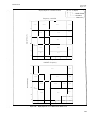
�
---- Earth
Plug : SEV 1 0 1 1 . 1 9 59-24507 Type 1 2, 2 5 0 V
Cable : H P 8 1 2 0 - 2 1 0 4
Denmark
� Line
Neutral
**
Plug : DHCR 107, 2 2 0 V
Cable : H P 8 1 20-2956
Plug option 905 is frequently used for
interconnecting system components and
peripherals.
N OTE : Each option number includes a ' family '
of cords and connectors of various materials and
plug body configurations (straight, 9 0 0 etc.).
Figure 2-2. Power Cables Supplied.
2-3
Section 11
Model 4 1 92A
Paragraphs 2-1 6 to 2-22
2-16.
The 4192A can be operated on a bench or can be
rack-mounted. The 4192A is ready for bench operation
as shipped from the fact ory. For bench operation, the
instrument is equipped with two retractable legs that are
l ocated on the bottom cover. They are extended by
pulling them away from the bottom cover.
2-20.
Operating Environment
Temperature. The instrument may be operated in
environments with ambient temperatures from 00 C to
+55°C.
2-17.
Humidit y . The instrument may be operated in
environments with rel ative humidities to 95 % at 40 ° C. 2·21. I nstallation of Options 907, 908 and 909
However, the instrument shoul d be protected from
temperature extremes which cause condensat ion within 2-22. The 4192A can be rack-mounted and operated as
the instrument.
part of a measurement system. Rack mounting informa
tion for the 4192A is given in Figure 2-3 .
2-18 .
2-19.
INSTALLATION INSTRUCTIONS
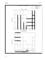
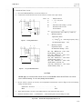
Op tion
907
!
Kit
Parts Included
Part Number
Part Number
Front Handle
Trim Strip
# 8-32 3/8 Screw
Handle Kit
5061-0091
x
908
Rack Mount Flange
3/8 Screw
Rack Fl ange Kit
# 8-32
5061-0079
L_�.
909
Rack Fl ange &
Handl e Kit
5061-0085
I
x
Front Handle
Rack Mount Flange
# 8-32 5/8 Screw
x
1.
Figure 2·3.
2-4
G) 5060-9901
8) 5060-8898
2510-0195
0
I
2510-0194
9.525
._
mm
2
2
6
15.875
mm
2
6
I
Remarks
�ll
.�
.
5020-8864
2510-0193
G) 5060-9901
® 5020-8876
Q 'ty
1
, ,,, m
__
Remove the adhesive-backed trim strip CD
from botb sides of the front-panel frame.
2.
H A NDLE INSTALLATION: Attach the
handles CD to both sides of the front-panel
frame with the screws provided, and attach
trim CV ·
3.
RACK MOUNTING: Attach rack mount
flange (3) to both sides of the front-panel
frame with the screws provided.
4.
H ANDLE AND RACK MOUNTING: Attach
front handle @ and rack mount flange (Bto
both sides of the front-panel frame with
screws provided.
5.
When rack mounting (3 and 4 above), remove
the four instrument feet (lift tab, and slide
the foot in the direction of the t ab).
Rack Mount Kits.
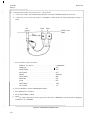
Section 11
Paragraphs 2-23 to 2-28
Model 4192A
2-23 .
STORAGE AND SHIPMENT
2-24.
Environment
2-25. The in strument should be stored in a clean , dry
environment. The following environmental limitations
apply t o both storage and shipment:
Temperature . . . . . . . . . . . . . . -55°C to +75° C
Humidity . . . . . . . . . . ' . . . . . to 95% (at 4 0°C )
The instrument should b e protected from temperature
extremes which cause condensation inside the instrument.
2-26.
Packaging
2-27. Original Packaging. C ontainers and materials
identical to those used in factory packaging are availabl e
through Hewl ett-Packard offices. If the instrument is
being returned to Hewlett-Packard f or serVicing, att ach a
tag indicating the type of service required, return address,
model number, and full serial n umber. Also mark the
container FRAGILE to assure careful han dling. In any
correspondence, refer to the in strument by model number
an d full serial number.
2-28. Other Packaging. The following general in struc
tions should be used for repackaging with commercially
av ail abl e materials:
a. .wrap in strument in heav y paper or plastic. If shipping
to Hewl ett-Packard office or serv ice center, attach tag
indicating type of service required, return address,
model n umber, and full serial n umber.
b . Use strong shipping container. A double-walled
carton made of 350 poun d test material is adequate.
c. Use enough shock absorbing material (3 to 4 in ch
layer) aroun d all sides of the instrument t o prov ide
a finn cushion and prevent mov ement inside con
tainer. Protect front-panel with cardboard.
d. Seal shipping container securely.
e. Mark shipping container FRAGILE to ensure care
ful handling.
f.
In any correspon dence, refer to instrument by model
number and f ull serial number.
2-5
Section In
Model 4192A
Paragraphs 3-1 and 3·2
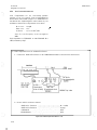
SECTION III
OP IRATlON
3-1.
ALL PROTECTIVE EARTH TERMINALS, EX
TENSION CORDS, AUTO-TRANSFORlII.ERS AND
DEVICES CONNECTED TO IT SHOULD B E
CONNECTED TO A PROTECTIVE EARTH
GROUNDED SOCKET. ANY INTERRUPTION OF
THE PROTECTIVE EARTH GROUNDING WILL
CAUSE A POTENTIAL SHOCK HAZARD THAT
COULD RESULT IN PERSONAL INJURY.
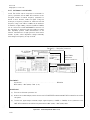
INTRODUCTION
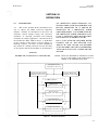
This section provides all the inf or mation neces
sary to opera te the Model 4 1 92A LF Impedance
Analyzer. Included are descriptions of the front- and
r ear-panel contr ol s, displays, lamps, and connectors;
discussions on operating procedures and measuring
techniques for various application s; and instructions on
the in strument's SELF TEST function. A break-down
of the contents of this section is given in Figure 3- L
Warnings, Cautions, and Notes are given throughtout;
they should be car efully observed to secur e the safety
of the operator and the serviceability of the instrumen t.
3-2.
ONLY FUSES WITH THE REQUIRED RATED
CURRENT AND OF THE SPECIFIED TYPE
SHOULD BE USED. DO NOT USE REPAIRED
FUSES OR SHORT CIRCUITED FUSEHOLDERS.
TO DO SO COULD CAUSE A SHOCK OR FIRE
HAZARD.
WARNING
Caution: Before the instrument is switched on, it must
be set to the voltage of the power source, or
damage to the instrument may result.
BEFORE THE INSTRUMENT IS SWITCHED ON,
Operating Instructions
(paragraphs
3-3 thru 3-33)
Impedance Measurement
Amplitude Phase Measurement
(paragraphs
(paragraphs 3-67 thm
3-34 thm 3-66)
r - Ext;;d;dCapa bUitles-
I
I
I
(paragraphs
I
I
I
I
I
- - -1
I
I
HP-lB Interface
I
I
-
3-109 thru 3-130)
I
I
I
:
Recorder Outputs
(paragraphs
3-1 3 1
thm
3-136)
I
I
I
I
I
I
I
;
I
I
:
I
I
I
L
External Synthesizer
(paragraphs
3-137 and 3-138)
:
I
I
1
Internal Control Switch
(paragraphs
_ _ _
Figure 3fi1.
-
3-139 and 3-140)
--
- -
3-108)
--
I
I
-
Contents of Section
-'
III
3-1
Section III
Model 4192A
Paragraphs 3·3 to 3·6
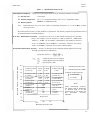
3-3_
OPERATING INSTRUCTIONS
3-5.
3-4, Operating in struction s for the instrument's basic
capabilities are given in paragraphs 3-5 through 3-33.
Operating instruction s f or extended capabilities (remote
operation via the HP-lB, X-Y Recorder Outputs, External
Synthesizer, and Internal Control Switches) are covered
in paragraphs 3-109 through 3-140.
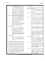
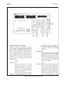
-==:-.".___
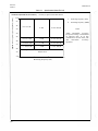
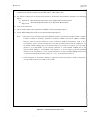
=
(D --if-+-
o
0
0
•
A A
0
3-6, Front- and rear-panel features are described in
Figures 3-2 and 3-3, respectively. More detail ed informa
tion on the panel displ ays an d controls is given starting in
p aragraph 3-7.
O,SPLAV
L,;I .U
Panel Features
� ___..,
/ A
J U
r-------,I
I
B O D O D O I]
. ";; cJ" ,,,'S "
,,
•.
" !lAI'G'
o G @] @]
eD
®
�
"'�
0
i
. .I
GGG
LINE O F F/ON
Applies ac line power to the in strument when set
to the ON position , Removes ac lin e power when
set to the OFF position.
Trigger Lamp:
Comes on each time the instrument is internally,
externally, or manually triggered. Trigger mode is
set by the TRIGGER keys <8 .
D ISPLAY A :
Displays the measured val ue of the p arameter set
by the DISPLAY A Fun ction Select Keys @) .
Also displ ays error codes and messages, SELF
TEST @ results, ZERO offset @ information ,
and the HP-IB address (0) in Figure 3-3). Maxi
mum 4Y2 digits; max imum display is 1 9999 for L
and C measurements, 1 2999 for other parameter
G)
measurements. Number of display digits depends
on OSC LEVEL @ and the measuring range.
Display ann un ciators light to indicate the units of
the displ ayed value.
D ISPLAY B :
Displays the measured value of the paramet er set
by the DISPLAY B Function Sel ect K eys @. If
the measurement cannot be made, OF2 or - - is displ ayed. When DISPLAY A Function @) is
set to A (dBm/dBV) or B (dBm/dBV), this dis
play is bl ank. Max imum 4% digits; maximum dis
play is 18000 for phase (8) measurements, 1 2999
for ot her parameter measurements. Number of
display digits depends on OSC LEVEL @ and
the measuring range. Display ann un ciators light
to indicate the units of the displ ayed value.
Figure 3·2. Front Panel Features (Sheet 1 of 10)
3-2
o
0
'"'0 �'�,"">L �
o
,�,
Mode1 4192A
®
o
Section HI
Figure 3-2
Test Parameter Data Display ( DISPLAY C ) :
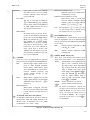
CHANN E L A ( R E F E R ENCE INPUT) Connector:
Displays test parameter values (FREQ. BIAS, and
OSC LEVEL). Test para meters are set by the test
PARAMETER Select keys @. Max imum 7%
digits for frequency; 4% digits for OSC LEVEL
and DC BIAS. Annun ciator l amps, l ocated to the
right of the display, light to in dicate the units of
the displayed value. Also displays errOr codes,
overflow annunciation, and in formation related
to the SAVE fun ction.
Used in conjunction with CHANNEL B 0 and
OSC OUTPUT @ in tran smission characteristics
measurements, i.e., gain/l oss (B-A), l evel ( A or
B), phase, group delay. The 5 H z - 1 3 MHz signal
from OSC OUTPUT @ is simultaneously appl ied
to the input port of the network under test and
t his connector. In put impedance, shunt capa
citance, and max imum in put voltage of CHAN
NEL A are the same as t hose of CHANNEL B 0.
B I AS ON Indicator:
CABLE LENGTH Switch:
C omes on when dc bias is a pplied to the DUT;
goes off when the BIAS OFF key @ is pressed.
This switch has meaning in impedance mea sure
ments only. It facilitates balancing of the measur
ing bridge circuit and minimizes measurement
errors when the stan dard I meter test l eads are
used.
CD 6f6%
Keys and Indicators:
These keys - one for DISPLAY A and one for
DISPLAY B -are used for deviation ( 6) or per
cent deviation (.6.%) measurement. For percent
deviation (6 %), the (8lue I key @ must be pressed
before the 6/6% key.
6 (Delta) : The difference between the measured
value of the DUT and a previously
stored reference value is displayed by
pressing t his key. The formula used to
cal culate t he deviation is
A-B
where A is t he measured value of the
DUT and B is the stored referen ce
value
The differen ce between the measured
6%:
value of the DUT and a previously
stored reference value is displayed as a
percentage of t he reference value.
The formula used to calculate the per
cent deviation is
A B X l OO (%)
B
I m:
Set the switch to this position when usin g
the standard I meter test l eads. A ppropriate
compensation is made for propagation delay
and phase error caused by the test leads in
high frequency measurements.
0: Set the switch to this position when using a
direct altachment type t est fixture ( connects
to the UNKNOWN terminals @).
DSC OUTPUT Connector:
@
where A is the measured value of the
DUT and B is the stored reference
value.
o
CHAN N E L B (TEST I N PUT) Connector:
Used in conjunction with CHANNEL A 0 and
OSC OUTPUT @ in transmission characteristics
measurements, i.e., gain/loss (B-A), level ( A or
B), phase, group delay. Output port of the net
work under test is connected to this connector.
Input impedance is I Mn ± 2%, shunted by 25 pF
± 5 pF. Maximum input voltage is AC 2 Vrms
and DC ± 35V.
@
Used in conjun ction with CHANNEL A 0 and
CHANNEL B 0 in tran smission chara cteristics
measurements, Le, gain/loss ( B-A), level ( A or B),
phase, group delay. Provides a 5Hz to 13 MHz
stimulus signal for the network under test (output
of n et work is connected to CHANNEL B 0) and
the referen ce signal for CHANNEL A 0. Output
impedance is approximately 50n.
U N K N OWN Terminals:
Used for impedance/phase measurements - I Z I ,
I Y I , R, G, L, C , X, B, phase - these four BNC
connectors provide the means to connect DUT's
-- components or n et works - in a four terminal
pair configuration : High current terminal (HcuR),
High potential terminal (HPOT), Low current
terminal ( LcUR ), and Low potential terminal
( LpOT). Four terminal pair test fixture attaches
directly to these terminals.
G ROUND Terminal:
This terminal is tied to the instrument's chassis
ground and can be used in measurements that
require guarding.
Figure 3.-2. Front Panel Features (Sheet 2 of 10)
3-3
Section HI
Figure 3·2
Model 4192A
r
o
0
�N��O"'N
0
0
,<�':&/>',��"":;_"
(It;C
tQJ
@
®
--
I
"
"'"
""
--- -
r
"'"
'M
"
--
' "'
-
-
-
'H,
;
"�J
-
"'�
" 0 ...0< 1
-
0
-
CABle
lON(lTH
®®®® �
MODE @ is set to � , the inst
rumen t measures I V I (absol ute value
of the DUT's admittance) and 0 (phase
angle) in degrees or radians; the re
sults are displayed on DISPLA V A
( IV I ) and DISPLA V B (0) to p rovide
a polar representation ( IV ILO) of the
DUT's admittance"
HP,IB Status Indicators and LOCAL key:
These four LED lamps - SRQ, LISTEN, TALK ,
and REMOTE - indicate the status of the 4 192A
when it is in terfaced with a con troller v ia the
HP,IE"
The LOC A L key, when p ressed, releases the in '
strument f rom REMOTE (HP,IB) control and
enabl es front-panel con troL The LOC A L key
does not f unction when the in strument is set to
l ocal l ockout by the controll er.
R/G:
DISPLAY A Function Select Keys and I ndicators:
These keys (QJ an d [ill
are used in con
junction with the C IRCUIT MODE keys @ to
sel ect the primary measurement parameter f or
display on DISPLAV A" The sel eetable parameters
are I Z I / I V I , R/G, L, C , B-A (dB), A (dBm/dBV),
or B (dBm/dBV)" The sel ected p arameter is in
dicated by the corresponding LED lamp" Pressing
either of these keys shif ts the sel ected parameter
in the indicated direction ( @] , [QJ )
I Z I / I V I : When C IRC UIT MODE @ is set to
A UTO or o-C:I-Wro , the instrument
measures I Z I (absolute v alue of the
DUT's impedan ce) and e (phase angle)
in degrees or radians (depends on DIS
PLAY A Fun ction ® setting); the
resul ts are displayed on DISPLA V A
( I Z I ) and DISP LA V B (0) to provide
a polar represen tation ( I Z ILO) of the
DUT's impedance" When C IRC UIT
-
"
L:
When C IRC UIT MODE @ is set to
the in strument measures R
(resistance of the D UT) and X (react
an ce of the DUT); the results are dis
played on DISPLA V A (R) and DIS
P LA V B (X) to provide a rectangular
(Cartesian) representation (R±jX) of
the DUT's impedance"
When C IRCUIT MODE @ is set to
� , the in strumen t measures G
(conductance) and B (susceptance);
the results are displayed on DISPLA V
A (G) and DISP LAV B (B) to p rovide
a rectangular (Cartesian ) represen ta
tion (G ±jB) of the DUT's admittan ce"
�,
Measures inductance and - depending
on the setting of DISPLA V B Func
tion ® Q (quality factor), D (dis
sipation f actor), or R/G (equiv al en t
series resistan ce or equivalent parallel
conductan ce [to measure G, C IRC UIT
MODE @ must be set to � \);
Figure 3·2. Front Panel Features (Sheet 3 of 10)
3-4
-
-
Section In
Figure 3·2
Model 4192A
the results are displayed on DISPLAY
A and DISPLAY B, respectively.
C :
Measures capacitance and depending
on the setting of DISPLAY B Func
tion ® - Q (quality factor), D (dis
sipation factor, or R/G (equivalent
series resistance or equivalent parallel
conductance [ to measure G, CIRCUIT
MODE @ must be set to � l ) ;
the results are displayed on DISPLAY
A 0 and DISPLAY B (�) respectively.
B-A (dB) : Measures the relative amplitude of the
reference input (CHANNEL A 0) and
the test input (CHANNEL B 0). The
result is displayed on DISPLAY A 0.
Also measures group delay or phase in
degrees or radians (selected by D IS
PLAY B Function ®).
The value displayed on DISPLAY A
o is the gain or loss of the network
under test. Group delay or phase is
displayed on D ISPLAY B 0.
A (dB m/dB V) :
Measures the absolute amplitude of
the reference input (CHANNEL A
0) in dBm or dBV (selected by GAIN
MODE Select key @). Amplitude
is displayed on DISPLAY AG).
When this parameter is selected, D IS
PLAY B Function ® has no select
able parameters and DISPLAY B 0 is
blank.
B (dBm/dBV) :
Measures the absolute amplitude of
the test input (CHANNEL B 0);
identical to A (dBm/dBV) in all other
respects.
DISPLAY B Function Select Key and Indicators :
This key [Q) , is used in conjunction with the
CIRCUIT MODE keys @ to select the secondary
measurement parameter for display on DISPLAY
B 0- Selectable parameters are e (phase), Q
(quality factor), D (dissipation factor), R/G (equi
valent series resistance or equivalent parallel con�
duetance), and GROUP DELAY. Phase (0) can
only be selected when DISPLAY A Function ®
is set to I Z I / I Y I or B-A (dB); Q, D, and R/G,
only when DISPLAY A Function is set to L or C ;
GROUP DELAY, only when DISPLAY A Func
tion is set to B-A (dB).
J
The selected parameter is indicated by the corres
ponding LED lamp.
Pressing this key shifts the selected parameter in
, the indicated direction ( @] ).
e (deg) : Measures, in degrees, the phase angle
of I z I (absolute impedance of the
DUT) or I Y I (absolute admittance of
the DUT).
e (rad) :
Measures, in radians, the phase angle
of I Z I (absolute impedance of the
DUT) Or I Y I (absolute admittance of
the DUT).
X/B :
These parameters are automatically
selected when DISPLAY A Function
@ is set to R/G. X is the reactance
of DUT's impedance ; B is the sus
ceptance o f the DUT's admittance.
Q :
Measures the quality factor of the
DUT. DISPLAY A Function ® must
be set to L (inductance) or C (capac
itance).
D :
Measures the dissipation factor of the
DUT. DISPLAY A Function ® must
be set to L (inductance) or C (capac
tance).
Measures the resistance or conductance
of the DUT. DISPLAY A Function
® must be set to L (inductance) or C
(capacitance). CIRCUIT MODE keys
@ detennine which of the two para
meters (R or G) is selected.
GROUP DELAY:
Measures the group delay between the
reference input (CHANNEL A 0)
and test input (CHANNEL B 0). Can
only be selected when DISPLAY A
Function ® is set to B-A (dB).
RIG :
e (deg) :
e (rad) :
Measures, in degrees, the phase differ
ence between the reference input
(CHANNEL A 0 ) and test input
(CHANNEL B G)l. Can only be
selected when DISPLAY A Function
® is set to B-A (dB).
Measures, in radians, the phase differ
ence between the reference input
(CHANNEL A 0) and test input
(CHANNEL B 0) Can only be
selected when DISPLAY A Function
@ is set to B-A (dB).
.
Figure 3·2. Front Panel Features <Sheet 4 of 10)
3-5
Model 4192A
Section HI
Figure 3·2
OISPLAV e _ mSPlILV �
o
0
0
0
0
f ''''rro
�'O �'I'-O/�
r:o ��w
,
�;)
i'O A<_�'
G ,,,,,, , O ,
! ' O ",,,,,illil'_
,,,
a"",O·
,,�;"-�'�f�
I@
@
l�\t
@@@@ �
Tes t PARAMETER Select Keys and Indicators:
These keys are used in conjunction with the
DATA input keys @, ENTER keys @ , and the
BLUE key ® to assign values to the various test
parameters; to monitor the test parameters; to
save and recall front-panel control settings; and to
input reference data for deviation and percent
deviation (M t;% 0) measurements. Pressing a
test parameter key will cause the value of the
selected test parameter to be displayed on the
Test Parameter Data Display @. Lighted indi
cator lamp (center of each key) indicates selected
test parameter. Only one test parameter can be
selected. Test parameters labelled in blue are
accessible b y first pressing the BLUE key @ .
SPOT FREQ/BIAS:
For single point measurements. Sets
the spot frequency and spot bias.
When spot bias is set, BIAS ON In
dicator @ lights.
@) @)
i;;;:]l!dlilEl
STEP FREQ/BIAS:
For swept measurements. Sets the
step (increment) frequency and step
(increment) bias.
START FREQ/BIAS :
For swept measurements. Sets the
start frequency and start bias.
STOP FREQ/BIAS :
For swept measurements. Sets the
stop frequency and stop bias.
OSC LEVEL :
Sets the voltage (rrns) o f the internal
frequency synthesizer.
REF A :
For deviation and percent deviation
(t;/ t;% 0) measurements. Sets the
reference value for DISPLAY A.
REF B :
For deviation and percent deviation
(!i/ t;% 0) measurements. Sets the
reference value for DlSPLA Y B .
Figure 3·2. Front Panel Features (Sheet 5 of 10)
3-6
Model 4192A
Section III
Figure 3·2
TEST LEVEL MONITO R Key and I ndicator:
Pressing this key displays the level of the test
signal applied to the DUT or, if the BLUE key
@ is first pressed, the current through the DUT
on the Test Parameter Data Display 0- The ap
propriate annunciator lamp will light.
DATA Input Keys:
These keys (0 thru 9, decimal point, and minus
sign) are used to input test parameter values,
register numbers for SAVE @ and RCL @
functions, and reference data for DlSPLAY A
(REF A) and DISPLAY B (REF B) deviation
measurements ( b. / l:>% 0). Data is displayed on
the Test Parameter Data Display 0- as it is input.
Each key has a con trol function - labelled in blue
above the key - which is accessible via the BLUE
key @. These control functions are explained
individually in 0 thru
@) .
E NT E R Keys:
These keys instruct the instrument to read the
test parameter data and reference data set by the
PARAMETER Select keys @ and DATA Input
keys
Data are not input until one of these
keys is pressed.
@.
MHz, V :
Enters the value input from the
DATA Input keys
in MHz for
frequency parameters or V for bias
parameters.
@
kHz, mV : Enters the value input from the
DATA Input keys
in kHz for
frequency parameters or ill V for bias
parameters.
@
Hz, REF DATA:
Enters the value input from the
DATA Input key
in Hz for fre·
quency parameters or as reference
data for deviation measurements.
@
RCL (Recall) Key:
This key is used to return the instrument to the
front-panel control settings, test parameter values,
calihration data (ZERO OPEN/SHORT @), and
reference data saved by the SAVE key @.
DATA Input keys
0 thru 4 are used t o select
the desired register. For example, to return the
instrument to the control settings stored in
I!"�/'"
.
� .
register 0, press
and m
@
'E:�r
SAVE Key:
This key is used to save (store) front-panel con
trol settings, test parameter values, calibration
data (ZERO OPEN/SHORT 0), and reference
data. There are five registers (0 thru 4), so five
sets of control settings can be saved. And because
the registers are nonvolatile, saved control settings
can be recalled (RCL key @) even if the instru
ment has been turned
off. To store existing conSI>VE/8EF
tr01 settings, press
and enter the register
'8
number from the DATA Input keys @ .
Figure 3·2. Front Panel Features (Sheet 6 of 10)
3-7
Section In
Figure 3-2
Model 4192A
o
0
0
0
0
SWEEP Control Keys and Indicator:
These keys control the instrument's sweep func
tion. Frequency, bias voltage, and oscillator level
can b e swept. (Oscillator level can be swept in
MAN. mode only.) BIAS ON Indicator eD must
be on for bias voltage sweep; off for frequency
sweep. The MAN AUTO key controls the sweep
mode. Indicator comes on in AUTO mode. The
functions of the other keys are described below
for each m ode. For log sweep, press the LOG
SWEEP key @).
AUTO
START UP :
Starts the frequency or bias voltage
sweep from the value set by the
START FREQ./BIAS test parameter
key @. Sweeps up at the increment
(step) set by the STEP FREQ./BIAS
test parameter key @ .
Also restarts the sweep after aPAUSE.
PAUSE :
Temporarily stops the sweep to allow
the sweep step or sweep direction to
be changed. Sweep is restarted by
pressing the START UP or START
DOWN key.
START DOWN :
Starts the frequency or bias voltage
sweep from the value set by the STOP
FREQ./BIAS test parameter key @.
Sweeps down at the increment (step)
set by the STEP FREQ./BIAS test
parameter key @. Also restarts the
sweep after a PAUSE.
MAN.
STEP UP : Each time this key is pressed, the fre
quency or bias voltage is incremented
by the value set by the STEP FREQ./
BIAS test parameter key @' If the
OSC LEVEL or TEST LEVEL MON
ITOR key is pressed, oscillator level
will be incremen ted by I mV (when
level is less than lOO m V) or 5 mV
Figure 3-2. Front Panel Features (Sheet 7 of 10)
3-8
Section III
Figure 3·2
Mode1 4192A
(when level is greater than 100 mV)
each time this key is pressed. Sweep
becomes continuous when this key is
pressed and held.
X I O STEP :
This key is used with the STEP UP
[Q] or STEP DOWN @) key. Holding
this key down while pressing STEP UP
or STEP DOWN increases the sweep
step value by a factor of ten.
STEP DOWN :
Each time this key is pressed, the fre
quency or bias voltage is decremented
by the value set by the STEP FREQ./
BIAS test parameter key @. If the
OSC LEVEL key or TEST LEVEL
MONITOR key is pressed, oscillator
level will be decremented by I m V
(when level is less than 100 m V) or
5 m V (when level is greater than
100 m V) each time this key is pressed.
Sweep becomes continuous when this
key is pressed and held.
TRIGGER:
These keys select the trigger mode for triggering
measurement (Internal, External or Hold/Manual) :
INT :
Internal trigger signal enables instru
ment to make repeated automatic
measurements. Measurement speed
varies depending on the type of meas
urement, oscillator frequency, and
whether normal, average, or high
speed is selected.
EXT :
Measurement is triggered by external
trigger signal through rear panel EXT
TRIGGER input connector ( (D in
Figure 3-3).
HOLD/MANUAL :
Measurement is triggered each time
this key is pushed. Measurement data
is held until the next time the key is
pressed.
ZY RANGE Select Keys and Indicator;
In impedance measurements, these keys select the
measurement range and ranging method of the
absolute value of impedance ( I Z I : 1 n - I M n)
or admittance ( I Y I : l OllS - l O llS).
AUTO (when indicator is lit) :
Optimum range for the sample value is
automatically selected.
MANUAL (when indicator is not lit) :
Measurement range is fixed (even
when the sample is changed). Manual
ranging is done by pressing adjacent
DOWN ( @) ) or UP ( [Q] ) key.
@) )
( [Q] )
key
or UP
Note: Pressing DO WN (
sets the ranging mode to Manual even if
the ranging mode was set to A UTa.
GAIN MODE Selector Key:
In amplitude/phase measurements, these keys
select the appropriate unit for A (absolute ampli
tude of reference input) and B (absolute amplitude
of test input).
Displays absolute amplitude in dBm
(=20 10g!O V + 13.01).
dBm :
Displays absolute amplitude in dBV
dBV :
(=20 log!o V)·
C I RCUIT MODE Selector Key:
These keys select desired measurement circuit
mode to be used for R/G, C, or L measurement.
AUTO :
o-t::::l-Wro :
�
:
Automatically selects appropriate parallel or series equivalent circuit for
the sample value. When ZY RANGE
@ up-ranges from the l kn ( I O ms)
range to 10 kn ( l ms) range, circuit
mode changes from o-Cl-Wroto � .
When ZY RANGE ® down-ranges
from the lOOn ( l OOms) range to
I O n ( l s) range, circuit mode changes
from � too-Cl-Wro.
Selects equivalent series circuit.
Selects equivalent parallel circuit.
Note: In I Z I /I Y I measurements, ranging does
not affect the measurement circuit mode.
CIRCUIT MODE keys are used to select
I Z l r I Y I . When the circuit mode is set
o
to A UTa or o-Cl-Wro ,
I Z I is selected;
when the circuit mode is set to
I Y I is selected.
�
.
Figure 3·2. Front Panel Features (Sheet 8 of 10)
3-9
Section III
Figure 3·2
Model 4192A
Ii
� Icc=
O"U _�.
'Ra
o
0
">l'.
0
WN"NOWN
'"" "'"0"
0
0
,� '�y:io;"���
r©
IJ
n
J n
==
0
��'!,\�
@@@@ �
!:�
GA'� "'0',,,
_
fiIIM
G GG
Note: The nine secondary functions,@thru@ of the DA TA Input keys@are accessible by first pressing the BLUE
key@
@
@
B IAS O F F Key:
This key disables internal de bias operation.
When this key is pressed, no de bias is applied to
the DUT and BIAS ON indicator 0 goes off.
SHORT :
Z E R O Offset Keys and Indicators:
These keys perfonn compensation for the residuals
present in the test fixture, test leads, and meas
urement circuit. ZERO offset can be performed
for one spot frequency only. If the spot frequen
cy in changed, ZERO offset must be performed
again.
OPEN :
If this key is pressed when the test
fixture or test leads are terminated
OPEN and the indicator is off, meas
ured value at this time is stored as
residual admittance (G + jB) data and
the indicator comes on. While the
indicator is on, compensation for the
residuals is made.
®
If this key is pressed when the test
fixture or test leads are SHORTed and
the indicator is off, measured value at
this time is stored as residual imped
ance (R + jX) data and the indicator
comes on. While the indicator is lit,
compensation for the residuals is
made.
AVERAGE Key and Indicator:
This key sets the 4192A to the average measure
ment mode. In the average measurement mode
(when the indicator is lit), measurement data has
a higher resolution and repeatability than meas
urement data in the normal or high speed meas
urement mode. This function is released by
repressing the key after pressing the Blue key ®
or by setting the 4192A to the high speed meas
urement mode @.
Figure �2. Front Panel Features (Sheet 9 of 10)
3-10
Section III
Figure 3-2
Model 4192A
®
(§)
®
UR -+t :
H I GH SPE E D Key and Indicator:
This key sets the 4 1 92A to the high speed meas
urement mode. In the high speed measurement
mode (when the indicator is lit), measurement
time is shorter (approximately Y2) than the
measurement time in the normal measurement
mode. This function is released by repressing the
key after pressing the BLUE key ® or by setting
the 4 l 92A to the average measurement mode.
@
S E L F TEST Key and Indicator:
This key initiates the instrument's SELF TEST
function. During SELF TEST (when the in
dicator is on), six tests, which check the basic
functional operation of the instrument, are auto
matically performed. The results (Pass or Fail)
are displayed on DISPLAY A G) When the SELF
TEST is completed, this mode is released auto
matically and normal measurement mode (indi�
cator is off) is set.
@)
X-V R EC O R D E R Function Keys and Indicator:
These keys eontrol the instrument's analog out
put capability. Voltage proportional to the
measurement results is output from the X-Y
RECORD OUTPUT connectors (see @ in Figure
3-3) located on the instrument's rear-panel.
Graphs cau be plotted with this capability.
ON :
OFF :
t+- LL :
Analog data representing the meas
urement results and test parameter
value (frequency/bias) are output
from the DISPLAY A, DISPLAY B,
aud FREQ./BlAS RECORDER OUT
PUTS on the rear-panel. Indicator
lamp is on in this state.
No analog data is output, and X-Y Re
corder zero- and full-scale adjustments
can be made. Indicator lamp is off in
this state.
@)
@
Provides a reference voltage (1 V) from
each rear-panel RECORDER OUT
PUT. Used for full-scale adjustment
of the X-V Recorder. When this key is
pushed, the recorder pen will be posi
tioned at the upper-right (X and Y are
maximum) of the plot area.
STOR E DSPL A/B Key:
This key simultaneously memorizes the measured
values displayed on DISPLAY A 0) and DIS
PLAY B CD as reference values for deviation
measurement.
LOG SWE E P Key and Indicator:
This key sets the log sweep mode. In the log
sweep mode (when the indicator is on), the fre
quency is swept at 20 steps/decade. The steps are
automatically selected at logarithmic regular
intervals between the decade of the START fre
quency and the decade of the STOP frequency.
STEP. FREQ. has no meaning in log sweep. This
function is released by repressing the key (after
pressing the BLUE key
SWEEP ABORT Key:
Gi)).
This key releases sweep frequency (bias voltage)
measurement and activates a spot frequency
measurement at the frequency (voltage) point
where the sweep is aborted.
B L U E Key:
This key is pressed prior to pressing a blue label
function key to interchange a normal key func
tion with a blue label function.
This key is pressed to access and release the func
tions and test parameters labeled in blue on the
DATA Input keys
Test PARAMETER keys
@, and the /',f'" % keysG)
e,
Provides a reference voltage (OV) from
each rear-panel RECORDER OUT
PUT. Used for zero-scale adjustment
of the X-V Recorder. When this key is
pushed, the recorder pen will be
positioned at the lower-left (X and Y
are zero) of the plot area.
Figure 3-2. Front Panel Features (Sheet 1 0 of 10)
3-1 1
Section HI
Figure 3-3
Model 4192A
0
0
,"r)tf���"
0
,."��L,,,
1111
I nn I
0
0)
CD
VCO OUTPUT Connector:
Female BNC connector; outputs a 40.000005 MHz
to 53 MHz signal from the internal synthesizer.
This connector is normally connected to the EXT
vca connector 0 with a short-connector.
EXT VCO Connector:
Female BNC connector; receives a 40.000005 MHz
to 53 MHz (input level : 0 dBm - 3 dBm) signal
t o generate the measurement frequency ( 5 Hz to
1 3 MHz). This connector can be connected to an
external frequency synthesizer for better ac
curacy, stability, and resolution; or to the instru
ment's internal synthesizer. Normally connected
to the VCO OUTPUT connector 0) with a short
connector.
0)
"
EXT R E F E R E N C E Connector:
Female BNC connector; receives a I MHz or
1 0 MHz reference signal from an external signal
source to improve the stability of the internal
synthesizer. Input impedance is approximately
0
®
o
1 MHz OUTPUT Connector:
®
HP-IB Control Switch :
Female BNC connector; outputs a I MHz square
wave (2 1 . 6 Vp-p) to phase-lock external instru
ments. Output impedance is approximately son.
This switch sets the instrument's HP-IB address
(0 - 30), data output format (A or B), and inter
face capability (Talk Only or Addressable).
Specific information on this switch is given in
paragrapb 3- 1 1 7.
CB
HP-IB Connector:
Twenty-four pin connector; connects the instru
ment to the HP-IB for remote operations.
o
EXT T R I G G E R Connector:
This connector is used to externally trigger the
instrument by inputting an external trigger signal.
TRIGGER key on front panel should be set to
EXT. Specific information is provided in para
graph 3-22.
son.
Figure 3-3. Rear Panel Features (Sheet 1 of 2)
3-12
Section III
Figure 3-3
Model 4192A
CD
CD
-
L I N E VOLTAGE SE LECTOR Switch:
These switches select the appropriate ac
operating voltage. Selectable voltages are
I OOV/ ! 2 0 V ± I O % and 220V ± I O % /240V ± 5 %
- 1 0 % (48 cv 6 6 Hz). Refer t o paragraph 2-8.
-
PEN LIFT connector :
Outputs pen up/down control signal.
When the 4 1 92A is set as follows, this
connector outputs a LOW level TTL
signal (pen down).
( l ) X-Y RECORDER key on the
front-panel is set to ON.
L I N E FUSE Holder:
Instrument's power-Hne fuse is installed in this
holder.
(2) START UP key or START
DOWN key is pressed when X-Y
RECORDER and SWEEP MAN/
AUTO keys on the front-panel are
set to ON.
1 00 V/ 1 2 0 V operation : 1 .25AT, 250V
(HP P/N : 2 1 1 0-0305)
220V/240V operation : 0.6AT. 250V
(HP PIN: 2 1 1 0-00 1 6)
At other times, this connector outputs
a HIGH level TTL signal (pen up).
Refer to paragraph 2-8.
®
@
-
L I N E Input Receptacle:
AC power cord is connected to this receptacle.
Refer to paragraph 2-10.
R EC O R D E R OUTPUTS Connectors:
These connectors output de voltages proportional
to the measurement display outputs and test fre
quency (or internal de bias voltage), and a pen
control signal for the X-Y recorder. Results of
swept (frequency of bias) measurements can be
plotted by connecting an X-Y recorder to these
connectors.
FREQ/BIAS connector :
Outputs voltage proportional to the
test frequency or internal de bias volt
age (from OV at START frequency/
voltage to I V at STOP frequency/
voltage). The output voltage is pro
portional to the logarithm of the fre
quency when LOG SWEEP is set to
ON.
DISPLAY B connector :
Outputs voltage proportional to the
value displayed on DISPLAY B.
Normalized value is I V (max.).
DISPLAY A connector :
Outputs voltage proportional to the
value displayed on DISPLAY A. Nor
malized value is I V (max.).
Refer to paragraph 3- 1 2 1 for specifics.
Figure 3-3. Rear Panel Features (Sheet 2 of 2)
3-1 3
Section HI
Paragraphs 3· 7 to 3·10
3-7.
Model 4192A
3-9.
S E L F TEST
3-8.
The 4 1 92A is equipped with an automatic self
diagnostic function that can be initiated at any time to
confinn normal operation of the instrument's basic
functions. The SELF TEST can be initiated from the
front-panel by pressing the BLUE key and tbe SELF
TEST key, or via HP-lE remote control (program code
S I ). When tbe SELF TEST is initiated (indicator lamp is
on), the six tests listed in Table 3-1 are automatically
performed and the results (pass code or one of the error
codes listed in the table) are displayed on DISPLAY A.
If n o errors are detected, PASS is displayed on DIS
PLAY A and the instrument is returned to normal
measurement mode (SELF TEST indicator is off). If
an error is detected, the corresponding error code is
displayed on DISPLAY A and the SELF TEST stops.
If the instrument fails the SELF TEST, contact the
nearest Hewlctt-Packard Service Office (see list at back
of this manual).
3-10. To facilitate operation, the instrument is auto
matically set to the following initial control settings each
time it is turned on:
Panel Controls :
D ISPLAY A . . . . . . . . . . . . . . . . . . . . . . . I Z I
DISPLAY B . . . . . . . . . . . . . . . . . . . . 0 (deg)
Test Parameter Data Display . . SPOT FREQ
BIAS . . . . . . . . . . . . . . . . . . . . . . . . . . OFF
ZERO OPEN . . . . . . . . . . . . . . . . . . . . OFF
ZERO SHORT . . . . . . . . . . . . . . . . . . . OFF
AVERAGE . . . . . . . . . . . . . . . . . . . . . . OFF
HIGH SPEED . . . . . . . . . . . . . . . . . . . . OFF
SELF TEST . . . . . . . . . . . . . . . . . . . . . OFF
X-Y RECORDER . . . . . . . . . . . . . . . . . OFF
LOG SWEEP . . . . . . . . . . . . . . . . . . . . OFF
SWEEP . . . . . . . . . . . . . . . . . . . . . . . . . OFF
CIRCUIT MODE . . . . . . . . AUTO ( o-e::J..w..o )
GAIN MODE . . . . . . . . . . . . . . . . . . . . dBm
ZY RANGE . . . . . . . . . . . . . . . . . . . . . AUTO
TRIGGER . . . . . . . . . . . . . . . . . . . . . . . INT
;;,;;;,% . . ' . . . . . . . . . . . . . . . . . . . . . . . . OFF
Note: An abbreviated SELF TEST, which includes test
1 (one second only). 2, 3. and 6 (at 1 00 /cH only)
of the standard SELF TEST, is performed each
time the instrument is turned on. During this
abbreviated SELF TEST. only error codes are
displayed.
z
Table 3-1.
Test Number
I niti.l Control Settings
4192A S E L F TEST
Description
Display
----- -----Fail
Pass
I
All numerical displays and indicator lamps on the front-panel come on
and remain on as long as the SELF TEST key is being pressed. Check
that all displays and indicator lamps are on.
2
Checks four RAM's (Random Access Memory).
P-02
E-20, E-2 1
Checks fourteen ROM's (Read Only Memory).
P-03
E-30 - E-43
Checks that the interrupt signal is present and that it is of the correct
frequency,
P-04
E-SO, E-S I
3
-----
:1 '�
F
4
_.
", illo",,''', ill ili, YW (Y� '�
RO', D"�'",)
,(,m"
Checks that the frequency setting of the internal synthesizer is nonnally done at each decade.
P-Ol *
P-OS
i
_...-
E-6 1 , E-62
P-06 E-70, E-7 1 , E-72
,
* P-O I indicates that test I has been completed. It does not mean that the instrument has passed test 1 . The
operator must determine whether the instrument has passed or failed this test.
6
3-14
Section III
Paragraphs 3 - 1 1 to 3-1 7
Mode1 4192A
Test Parameters :
SPOT FREQ . . .
STEP FREQ . . .
STOP FREQ . . .
START FREQ .
OSC LEVEL . . .
SPOT BIAS . . .
STEP BIAS . . . .
START BIAS . .
STOP BIAS . . .
REF A . . . . . . .
R� B . . . . . .
3-11_
. . . . . . . . . . . . . . . . 100 kHz
. . . . . . . . . . . . . . . . . . 1 kHz
. . " . . . . . . . . . . . . 1 3 MHz
. . . . . . . . . . . . . . . . . . . S Hz
. . . . . . . . . . . . . . . . . 1 Vrms
. . . . . . . . . . . . . . . . . . . . OV
. . . . . . . . . . . . . . . . . . . . 1V
. . . . . . . . . . . . . . . . . . - 3S V
. . . . . . . . . . . . . . . . . . +3S V
.......... ........... 0
........ ..... . . . .... O
D isplays
3- 1 2. The 4 1 92A has three display sections: DISPLAY
A, D ISPLAY B, and a Test Parameter Data Display (here
inafter called DISPLAY C). DISPLAY A and DISPLAY
B are the primary displays; they are described in para
graphs 3 - 1 3 and 3-14, respectively. DISPLAY C is
described in paragraph 3- I S. The BIAS ON Indicator is
described in paragraph 3- 16.
3- 1 3. DISPLAY A provides direct readout of the
primary measurement parameter in amplitude/phase
measurements and impedance measurements.
In impedance measurements, DISPLAY A displays the
absolute value of the vector impedance, IzI ; the absolute
value of the vector admittance, j YI ; resistance, R; con
ductance, G ; inductance, L; or capacitance, C. In ampli
tude/phase measurements, DISPLAY A displays the
measured value of B-A (dB), the gain or loss between
CHANNEL A and CHANNEL B ; A (dBm/dBV), the
amplitude of the signal input to CHANNEL A ; or B
(dBm/dBV), the amplitude of the signal input to CHAN
NEL B.
All values are displayed with a maximum of 4Y2 digits.
The actual number of display digits depends on the
setting of other control functions such as OSC LEVEL,
ZY RANGE, etc. Maximum display is 1 9999 for in
ductance and capacitance measurements; 1 2999, for all
other parameters. Decimal point and the appropriate unit
annunciator (e.g., pF, mH, M S, Mil) are also displayed.
If the selected measurement cannot be made, because the
value of the DUT is outside the tnstrument's measure
ment range or because the front-panel controls are in
correctly set, one of the following will be displayed.
OF l
OF2
VCL
E-06
E-07
these annunciations. When a SHORT or OPEN ZERO
offset adjustment is being made, CAL is displayed. DlS
PLAY A also displays the pass- and error-codes (P-O I
through P-06 and E-20 through E-73) related to the
instrument's SELF TEST function. Refer to Table 3-4
for the meanings of SELF TEST error-codes E-20 through
Ef73.
3-14. DISPLAY B provides direct readout of the
secondary measurement parameter in amplitude-phase
measurements and impedance measurements. This dis
play is blank when DISPLAY A function is set to A
(dBm/dBV) or B (dBm/dBV).
In impedance measurements, DISPLAY B displays the
value of the impedance/admittance; phase angle, e
(degrees or radians); reactance, X; Sllsceptance, B ;
quality factor, Q ; dissipation factor, 0 ; resistance, R ; or
conductance, G.
In amplitude/phase measurements, DISPLAY B displays
either group delay or phase difference, e (degrees or
radians).
Refer to paragraph 3- 1 3 for specifics on number of digits,
maximum display, unit annunciators, etc.
If the. selected measurement cannot be made, OF2 or
- - is displayed. Refer to Table 3-3 for the meaning
of these annunciations.
3- l S . DISPLAY C displays all test parameter data
SPOT FREQ/BIAS, STEP FREQ/BIAS, START FREQ/
BIAS, STOP FREQ/BIAS, OSC LEVEL, TEST LEVEL,
and REF A or REF B value. Frequency is displayed with
a maximum of 7Y2 digits; BIAS, OSC LEVEL, and TEST
LEVEL are displayed with a maximum of 4 digits; and
REE A and REF B values are displayed with a maximum
of 4% digits. Error-codes displayed on DISPLAY C are
discussed in paragraph 3-17.
3- 1 6. The BIAS ON Indicator comes on to warn the
operator that the instrument is applying a de bias voltage
across the DVT.
3 - 1 7 . Error-codes and annunciations related to operator
error and out-of-range measurement are listed and de
scribed in Tables 3-2 and 3-3, respectively. Error-codes
for errors detected during SELF TEST are listed and de
scribed in Table 3-4. If the instrument fails the SELF
TEST, i. e., if one of the error-codes listed in Table 3-4 is
displayed on DISPLAY A, contact the nearest Hewlett
Packard Sales/Service Office.
Refer to Tables 3-2 and 3-3 for the meaning of each of
3-1S
Section III
Tables 3-2 and 3-3
Model 4192A
Table 3-2_
Operational Errror-codes
Error�code
Meaning
An attempt was made to input a test parameter value or reference value that is Qut-of-range.
E-OI
-
E-02
-----."'��-----
i-§
----
E-03
E-04
-------,-----------'''' ------'''- " -
-
i
--------------"-
--
-
-
-- -----"""----
I,
J
-_...........
E06
--
-
--------,,�'"''
I
E-08
I
-
E-09
--- --_._----- - -
-
The STORE DSPL A/B key was pressed when DISPLAY A and/or DISPLAY B is set to /:,//:,%
r:: _m�' m ;, <lli,M,m, 0" , 0"', Uo', m -
--- -----.-
-----
�-
------
"
..--------
.
-
..._--
-
REF A, REF B, I:!. , or I:!.% key was pressed when no reference data for the deviation measurement is stored.
_"" __•__••________•_______________,,________'''''''___
"_
,,
E07
�
-- -�
MAN SWEEP was attempted when the SPOT FREQ. (or BIAS) is lower than the START FREQ.
(or BIAS) or higher than the STOP FREQ. (or BIAS).
E-05
---- -
----
AUTO or MAN SWEEP was attempted when the STOP FREQ. (or BIAS) is lower than the
RT FREQ. (or BIAS).
- - ----, --- - � - ---- -- .-.----
-
- ---------
AUTO SWEEP was a!tempted when the selected test parameter was REF A, REF B, OSC
LEVEL, or TEST LEVEL MONITO R ; or MAN SWEEP was attempted when the selected test
parameter was REF A or REF B .
m__
_,,_
ZERO OPEN or ZERO SHORT operation could not be properly performed.
SAVE 5 - 9 or RCL (Recall) 5 := 9 was atte;':;pted (o�;
.._ - -
- ----_
---
- _._...--_._---
---
RCL (Recall) was attempted on an empty memory.
; memory locations 0 - 4 are available).
- -
--
._-
----
In swept frequency measurements of Group Delay, STEP FREQ. is too low for the START
FREQ'/STOP FREQ. sweep range.
E-1 O
Table 3-3. Annunciations (Sheet 1 of 2)
Meanings
DISPLAY
B
A
DISPLAY A
-
OFI
D ISPLAY B
Measured value of I Z l or I Y I exceeds 1 3 0 % of full scale of the ZY
RANGE.
Measurement cannot be performed.
OF2
Significant value
Measured value exceeds 200% of full
scale of display range.
Measurement is perfonned correctly.
Significant value
OF2
Measurement is perfonned correctly.
Measured value exceeds 200% of
full scale of display range.
OF2
OF2
Measured value exceeds 200% of full
scale of display range.
Measured value exceeds 200% of
full scale of display range.
The instrument's internal measurement circuit is saturated.
Measurement cannot be performed.
*1
UCL
3-16
-
-
-
Section III
Tables 3·3 and 34
Model 41 92A
Table 3·3.
DISPLAY
1--'
r--'-'--
A
B
Significant value
-
-
I
Annunciations (Sheet 2 of 2)
Meanings
DISPLAY
DISPLAY B
Measurement is performed correctly.
Measurement cannot be performed
because:
0 When function is set to
e. Q. or
D, the measured value of I Z I or
I Y I is less than 5% of full scale
of the ZY RANGE.
0 When GROUP DELAY measure-
ment is being performed, the
test frequency to be automatically selected next is outside
the selectable test frequency
range (5 Hz and 1 3 MHz).
-
-
-
-
-
-
Significant value
CAL
Auto ranging of ZY RANGE is being performed.
Measurement is perfonned correctly.
Blank
.
�""""�-..
D ISPLAY B function is blank when
DISPLAY A function is set to A
(dBm/dBV) or B (dBm/dBV).
ZERO offset adjustment is being performed.
* L When the measuring frequency is set to 1 0MHz or above and ZY RANGE is held; measured values output
500ms after DISPLAY A indicates "UCL" are invalid.
*2. Specific information on GROUP DELAY measurement is provided in paragraph 3-63.
Table 3-4
Display
SELF TEST E rror-codes
Meaning
E-20, E-2 1
One of the four RAM's (Random Access Memory) is not functioning properly.
E-30 - E-43
One of the fourteen ROM's (Read Only Memory) is not functioning properly.
---- "-,, .
E-50, E-5 1
E-6 1 , E-62
E-70, E-7 1 , E- 7 2
'
-" -
"-----�-�,..
-
--
The line frequency detection circuit is not functioning properly,
I
'
- ''-",.
Integrator in the VRD (Vector Ratio Detector) is not functioning properly.
-,---,,-��
_.,.
-.-
Internal synthesizer is not functioning properly.
3-1 7
Model 4192A
Section IJI
Paragraphs 3 · 1 8 to 3-21
3-18.
(1)
Test Signal
3-19. The internal frequency synthesizer provides a
sinusoidal wave test signal that has an accuracy of 5 5 ppm.
The frequency range is from 5 Hz to 1 3 MHz, and signal
level is 5 mVrrus to 1 . 1 Vrrus. The test signal is output
from the OSC OUTPUT connector (HCUR of the UN
KNOWN terminals) on the front-paneL Test frequency
and test level range, resolution, and accuracy are given in
Table 3-5.
Note: Test signal accuracy, stability, and re.'v)[ution can
be improved by connecting an external frequency
synthesizer to the EXT VCO connector on the
rear-panel. Specific information on measurements
using an external synthesizer is given in paragraph
(2) HIGH SPEED Measurement Mode:
This mode is set by pressing the HIGH SPEED
key. Measurement speed in this mode is approx.i
mately twice that of the NORMAL mode; how
ever, resolution is reduced and accuracy is not
specified. Integration time is 2 . 5 ms. Line fre
quency ripple is not rejected (filtered).
(3)
3-137.
Note: In impedance measurements, the level of the test
signal across the DUT depends on the impedance
of the DUT. To monitor the actual level of test
signal across the DUT, press the TEST LEVEL
MONITOR key. (Refer to paragraph 3-91 for
specifics. )
3-20.
3-2 1 . The 4 1 92A has three selectable measurement
modes: NORMAL, HIGH SPEED, and AVERAGE.
-
�
-------
-----
,-
Measurement Frequency
I
Frequency and Output level of Test Si gnal
Setting Range
5 Hz -
1 0 kHz
1
100 kHz -
I MHz
I OOmHz
-
1 3 MHz
1 Hz
'2
3-1 8
At 23CC ± 5°C.
"
Setting Value ± 50 p pm.
_.
I mVrms
5 Hz - I MHz: (5 + 1O/f)% + 2mV
I MHz - 1 3 MHz: (4 + 1 . 5[)% + 2mV
5mVrms
5 Hz - I MHz: (5 + 1O/f)% + IOmV
I MHz - 1 3 MHz: (4 + l . 5F)% + IOmV
__"','"
I
Setting Accuracy
I mHz
I O mHz
l OOmVrms - I . I Vrms
'1
Resoluti on
100 kHz
5 m Vrms - l OO mVrms
OSC Output Level ' 2
AVERAGE Measurement Mode:
This mode is set by pressing the AVERAGE key.
Resolution, accuracy, and repeatability in this
mode are much better than in NORMAL mode or
HIGH SPEED mode. The displayed measurement
value is the average of seven measurements. In
tegration time is 1 0 times the period of the line
frequency. Line frequency ripple is rejected
. (filtered).
Note: Measurement times for each mode at each
DISPLA Y AlE function setting are given
in paragraph 3-55 for amplitude/phase
measurements and in paragraph 3-89 for
impedance measurements.
Measurement Modes
Table 3-5,
NORMAL Measurement Mode:
This mode is automatically set each time the
instrument is turned OIl. In this mode, the in
tegration time of the instrument's AID converter
is equal to the period of the line frequency. Line
frequency ripple on the de voltage used for in
tegration is rejected (filtered).
UNKNOWN terminals open (impedance measurements) o r terminated with son (amplitude/phase measurement), f: measurement frequency (Hz), F : measurement frequency (MHz).
Section IH
Paragraphs 3·22 to 3·28
Model 4192A
3·22.
3·24.
Trigger Modes
3-23. The 4 192A has three selectable trigger modes:
INTERNAL, EXTERNAL, and HOLD/MANUAL.
(I)
(2)
(3)
INTERNAL Trigger Mode:
In this mode, measurement is automatically and
repeatedly triggered. Trigger speed depends on
the type of measurement, test frequency, and
measurement mode.
EXTERNAL Trigger Mode:
Measurement is triggered by applying a TTL level
pulse to the EXT TRIGGER connector on the
rear-panel. Refer to Figure 3-4 for specifics.
3-25. The 4 1 92A provides eleven test parameters. They
are listed, along with range and resolution, in Table 3-6.
Use the following procedure to set the value of these
parameters:
( I ) Press the desired PARAMETER key.
(2)
Note: Parameter values can also be set via the
HP-lB.
Refer to paragraph
specifics.
3-123
for
Note: If the parameter value is out-ai-range
(see Table
3-6). E-01
will be displayed
on DISPLA Y C for approximately one
Note: Measurement can also be triggered via the
Note:
Set the desired value with the DATA keys. The
set value will be displayed on DlSPLA Y C.
(3) Press the appropriate ENTER key to enter this
value.
HOLD/MANUAL Trigger Mode:
Measurement is triggered each time the HOLD/
MANUAL key is pressed. Measurement data is
held until the next time the key is pressed.
HP-lB. Refer to Figure
Setting Test Parameters
second and the previous value is retained.
3-38.
Triggering in EXT and HOLD/MANUAL
modes must be slow enough to allow the
instrument to complete each measure-
3�26.
Deviation Measurement
ment. If a trigger signal is received before
measurement is completed, it is ignored.
Input Levels :
2 V < VIH < 5 . 5 V
O V ';;: V1L < O.6V
Input Current :
Maximum I mA
(at VIH 5.5 V)
=
Low Level Input Current: Maximum -O.6mA
(VIL OAV)
=
Pulse Width :
Tp :2: 1 msec
Trigger Timing :
Leading Edge
Figure 3-4.
External Trigger Pulse
3-27. When many components of similar value are to be
tested, it may be more practical to measure the difference
between the value of the component and a predeter
mined, or ideal, reference value than measuring the DUT
value itself. When the purpose of the measurement is to
observe the change of a component's value versus changes
in temperature, frequency, bias, etc., a direct measure
ment of this change (deviation) makes examination more
meaningful and easier.
3-28. Deviation measurements can be made for either
or both DISPLAY A and/or DISPLAY B parameter meas
urements. There are two methods of inputting reference
values for deviation measurements: 1 ) input the refer
ence value using the DATA keys, or 2) input the meas
ured value of the reference component by pressing the
STORE DSPL A/B key. Deviation is displayed as either
the deviation (6) from the reference value or the percent
deviation (L'.%).
(l)
Deviation Measurement L'. (Delta):
The difference between the measured value of the
DUT and a previously stored reference value
(REF A or REF B) is displayed. The formula
used to calculate the deviation is
A-B
where A is the measured value of the OUT and B
is the stored reference value.
3-19
Section 1II
Mode1 4192A
Paragraph 3·29
Table 3·6.
I
Parameter
SPOT FREQ
Test Parameters
The spot frequency
START FREQ
The start frequency for swept frequency
measurements
STOP FREQ
The stop frequency for swept frequency
measurements
.�-..,�
-.
� ----
-
STEP FREQ
SPOT BIAS
-".
-
-
-
Range
5 Hz - 1 3 MHz
Range :
Resolution : 1 mHz at 5Hz - 1 0 kHz ;
l O mHz at 1 0 kHz - 1 00kHz;
1 00 mHz at 100 kHz - 1 MHz;
I Hz at I MHz - 1 3 MHz
--,--�----
The step frequency for swept frequency
measurements
--
Range :
Resolution:
--
----
--
-
--
-
-
-
-- ---
..
1 mHz - 1 3 MHz
1 mHz at 1 mHz - 1 0 kHz;
l OmHz at 1 0 kHz - 100kHz;
1 00 mHz at 1 0 0 kHz - 1 Mllz;
1 Hz at 1 MHz - 13 Mllz
-- ----
The start voltage for swept voltage measure�
ments
- --- - --- -- - - "" .
The stop voltage for swept voltage measurements
STOP BIAS
STEP BIAS
- - ---
--- -,�. -,.,.
The spot bias voltage.
START BIAS
I
Description
- 3 5 V - +3 5 V .
Range :
Resolution: l OmV.
..... _-
The step voltage for swept voltage measurements
Range:
Resolution :
OSC LEVEL
The level (rms) of the signal output by the
internal synthesizer
Range:
5 mV - 1 . 1 V.
Resolution: I mV at 5 mV - IOOmV;
S mV at 100mV - 1 . 1 V
REF A
The reference value for DISPLAY A devia·
tion measurements
REF B
The reference value for DISPLAY B devia·
tion measurements
.
(2) Percent Deviation Measurement to % (Delta Per·
cent):
The difference between the measured value of the
DUT and a previously stored reference value
(REF A or REF B) is displayed as a percentage of
the reference value. The formula used to calcu
late the percent deviation is
.!L...JL X 100 (%)
B
where A is the measured value of the DUT and B
is the stored reference value.
3-20
l Om V '\, 35V.
l OmV.
Range and resolution are the same as those of
the DISPLAY A/B parameter.
3-29. Use the following procedure to perform deviation
measurements:
(1)
Set the front-panel controls for normal amplitude
phase or impedance measurement. (Basic proce
dure for amplitude-phase measurement is given
in Figure 3 - 1 0, and in Figure 3-30 for impedance
measurements. )
(2)
Press the BLUE key and the REF A or REF B
key. At this time, the previously stored reference
value or E-06 will be displayed on DISPLAY C.
E-06 simply means there is no reference data for
Model 4192A
Section ITI
Paragraphs 3·30 to 3·33
the selected display function; ignore it and pro
ceed to step 3 .
(3)
Enter the desired reference value using the
numeric DATA keys. (E-06 annunciation will dis
appear.) This value will be displayed on DIS
PLAY C.
(4) Press the ENTER key labeled REF DATA. This
stores the value displayed on DISPLAY C as the
reference value.
Note:
To store the measured (displayed) value
of a reference sample (DUT) as reference
storage registers. These registers are used to store five
different. frequently used front-panel control settings.
Stored control settings are preserved (not erased) in the
registers even when the instrument is turned off.
Frequently used control settings can be saved and then
recalled instead of having to feenter the measurement
conditions each time. This feature improves efficiency in
applications where repetitive measurements are made.
Almost all front-panel control settings and test parameter
settings, including reference data and zero calibration
data, can be saved. Exceptions are listed below.
HP-IB status
DISPLAY A/B measurement data
LINE OFF/ON
CABLE LENGTH
BIAS ON
SPOT BIAS
data, use the following procedure:
(a)
Connect the sample to the instrument and
make one measurement.
(b)
Press the BLUE key and the STORE
DSPL A/B key. The values displayed on
DISPLA Y A and DISPLA Y B will be
stored as REF A and REF B data, respec
tively.
(5 ) Press the M/::,.% key on DISPLAY A and/or DIS
PLAY B. The value displayed on the display (A
or Bl is the difference (deviation) between the
stored reference value and the measured value.
For percent deviation measurement, press the
BLUE key before pressing the I:o.//::,. % key.
Note: Reference data stored for one measure
ment function cannot b e used for another
measurement function; that is, reference
data stored for an impedance measure
ment cannot be used for a resistance
measurement.
3-32. Use the following procedure to save and recall
a measurement condition :
(1)
Set the front-panel controls and test parameters
as desired.
(2)
Press the SAVE key and the register number
(0-4). All front-panel control settings and test
parameter settings are now saved, or memorized,
in the specified register.
(3) To restore the instrument to the control settings
and test parameters saved in step (2), press the
RCL key and the register number.
3-33. The instrument is equipped with two rechargeable
batteries that provide power for the storage registers
when the instrument is turned off. They are automatical�
Iy recharged while the instrument is turned on. Specifica
tions are given below.
Operating time:
7500 hours (typical) after full
charge.
3-30.
Continuous Memorization of Control Settings
(SAVE and RCL Functions)
Recharge time:
Time required to fully recharge
the batteries is 200 hours.
3-3 1 .
The 4 l 92A is equipped with five non-volatile
Lifetime:
5 years (at 25 ° C).
3-2 1
Section III
Model 4192A
Paragraphs 3-34 to 3-39
Table 3-8.
AMPLITUDE/PHASE MEASU R E MENT
3-34.
3-35. The Model 4 192A LF Impedance Analyzer can
accurately measure the gain/l oss, phase, group delay and
level of many types of circuits. It displays all measured
parameter s with 4% digit numeric displ ays. The built-in
frequency synthesizer can be set to any test frequency
between 5.000Hz and 1 3 .000000MHz, and can be
swept within that frequen cy range with 1 mHz (maxi
mum) r esol ution . Instructions f or amplitude/phase meas
urements are given in paragraph 3-34 to 3-66.
3-36.
B-A
A/B (dBm)
---
GROUP
DELAY"
Resolution
-
--
i
-
-
�
-
-
-
-
1
_
-�--
--
�
�
----_..-
I
�
--
6
6
..-
(deg)
(rad)
..
�,,�--.
- 1r
1r
3-39. The 4 1 92A can measure tr ansmission parameters,
gain /loss (B-A), level (A/B), phase ( 6 ) and group delay,
over the measurement ran ges listed in Table 3-8.
Measurement resolutiou, al so listed in the t abl e, are for
NORMAL and AVERAGE measurement modes.
Resolution in H IGH SPEED measurement mode is one
digit l ower t han these values.
* I:
Measurement range at GROUP DELAY is deter
mined automatically by LlF ( STEP FREQ X 2) and
LIB. Specific information on GROUP DELAY meas
urements is provided in par agraphs 3-63 to 3-66.
DISPLAY A/B Functions for Amplitude/Phase Measurements
Table 3-7.
D I SPLAY B Function
DISPLAY A Function
GROUP DELAY
0 (deg)
6 (rad)
Relative A mplitude of the Reference
Input an d the Test Input
--
-
""""
-�
-
"""""""
-
"
-. .
'
.-�"'--
.
i
..----- -------
-
�
----....
....--- ---:--
.----- -------
-.
B (dBm/dBV) Absol ute A mplitude of the Test Inp ut
Group Del ay in seconds
Phase Difference in degr ees
Phase Difference in radians
� ----
A (dBm/dBV) . Absol ute A mplitude of the Refer en ce Input
3-22
-
--
-
Measurement Ranges
1------ -
-�
A/B (dBV)
. _ -+
i 0 .00 1 dB
20dB
1 00 dB) --+-i 0.01 dB
.--' -- - - --1
+ 1 3 � dB111 � - 20 tIBJl1 �0 1 dB �
_
_
___
__
- 20dBm - - 87 <IBm i 0.0 1 dBrn
�
-+O� dBV
� - 20dBV O OOi dB V
8
20d E\! : - 1 00dB�To.oidBv
0.0001 I1s - 1.9999I1s
l OOps
I----Ins
O . OOl l1s 1 9.99911S
IOns
O.Ol l1s � 1 99 9911s
1.9999 ms
l OOns
i 0.000 I ms
II 0.001 ms � 1 9.999ms
IllS
0.01 ms 1 99.99ms
l OllS
r-'
- '
O.OOOl s - 1.9999s
1 00l1s
0.00 I s - 1 9.9995
Ims
-r---0° - ± 180°
0.0 1 °
- - 1.000
0.001
0.000 1
- I.0000 - + 1 .0000
+ 1.000 - +
0.001
OdB
± -(20dB -
-�--- -
3-37. Most amplitude-gain measurements are based on
relative measurements where the sign als at the input an d
output ports of a network are compared to determine
how the n etwork behaves as a sign al processor . The
4 1 92A simultaneously measures two independent, com
plementary parameters in each measurement cycle. These
measurement functions are classified, for displ ay purpose,
into two groups: DISPLAY A and DISP LAY B func
tions, as given in Table 3-7. Measur ement results can be
displayed as deviation or percent deviation from stored
r eference val ues. Deviation measur ements are described
in paragraph 3-26.
B - A (dB)
Measurement
Range
Measurement
Function
Measurement Functions
3-38.
Measurement Range for Amplitude
Phase Measurements
Model 4192A
3-40.
OSC OUTPUT
3-4 1 . In amplitude/pi:h1se measurements, the output
signal from the OSC OUTPUT terminal is applied to a
power splitter (HP Part No. : 0 41 9 2-61 0 0 1 , furnished
with the 41 92A) to produce two output signals that are
in phase and of equal amplitude. One of these signals is
applied to CHANNEL A and is used as the reference
input; the other signal is applied to input port of the net
work under test. The output port of the network is then
connected to CHANNEL B. Figure 3-5 shows the equiv
alent circuit for the OSC OUTPUT. The circuit consists
of a low (zero) impedance source in series with a s o n
resistor which determines the output impedance. The
output signal level is variable from 5 mV to 1 . 1 Vrms
when terminated with 50n. Specific information on the
internal synthesizer is provided in paragraph 3-1 8.
3-42.
Section III
Paragraphs 3-40 to 3·45
CHANNEL A/B
3-43. For basic amplitude/phase measurements, the
reference input is obtained by connecting one of the
output signals from the power splitter connected to the
OSC OUTPUT. The test input is obtained by inserting the
network to be tested between the power splitter and
CHANNEL B. Since the signals divided by the power
splitter are identical, the signal applied to CHANNEL A
represents the input to the network while the signal
applied to CHANNEL B is the output of the network.
By comparing these two signals, the 4 1 92A measures the
gain or loss, phase shift and group delay introduced by
the network. When the frequency is swept over the band
of interest with amplitude, phase and group delay, meas
urement data represent the amplitude and phase response
of the transfer function in the frequency domain.
3-44. For production testing, it is often necessary to
compare a newly manufactured network to a production
standard. The 4 1 92A, being a dual channel instrument,
lends itself well to this application. When comparing
two networks, the standard network is connected be
tween the power splitter and CHANNEL A to obtain
the reference. The network to be tested is then con
nected between the power splitter and CHANNEL B .
In this case, the 4 1 92A compares the output signals
of the two networks and any differences between the
networks are renected as deviation from O dB (B·-A
amplitude), 0 degrees (phase) or O s (group delay).
Zo = SOil
[OsCI
�
Low
Impedance
Source
Figure 3·5.
Equivalent Output Circuit
3-45. Figure 3-6 shows the equivalent circuit for the
CHANNEL A/B. The resistor, Rin, represents the I M n
input resistance; the capacitor, Cs, represents the 2SpF
± 5pF shunt capacitance. This high input impedance has
a minimum loading effect on the input signal and allows
the 4 1 92A to be used for characterizing networks having
output impedances other than 50n. Figure 3-7 shows
the input impedance, Z t , as a function of frequency. At
low frequencies, the reactance of Cs is very high, making
Z t nearly equal to Rin. As frequency increases, the
decreasing reactance of Cs becomes more and more
significant, causing Z t to decrease. At high frequencies,
Rin is no longer significant and Z t is slightly less than the
reactance of Cs (approximately 500n at 1 3MHz).
CHANNEL
A/B
I�
r-..
..I.pL
Rin
IMn
l7
�
Figure 3�6.
l7
,
Equivalent Input-Circuit
!
Cs
25pF
3-23
Section III
Paragraphs 3·46 and 3-47
Model 4192A
�
�
l OOkfl
N
I
� lOk)]
I
,I
\
100Hz
1 kHz
I
10kHz
�
lMHz
100kHz
Note :
3-47. Figure 3-8 illustrates and describes the basic input
configurations for various types of measurements. Con
nections of these input configuration,s should be made
using double·shielded cables with BNC connectors as
listed in Table 3-9. When making input connections,
observe the following guidelines:
( 1 ) Keep input cables as short as possible.
(3) When impedance terminations are required, use
shielded terminations equipped with suitable RF
connectors as listed in Table 3-1 0. Place termi
nations at the end of the transmission line.
1
___
_
3-24
I
�
1 20 cm BNC (male) - BNC (male) Double
- Shield Cable (two l l 1 70C's are furnished with the 4 l 92A)
">--__w._- CH. A
">----- CH . B
pa s s i ve power
spl i tter
Model No.
60cm BNC (male) - BNC (male) Double
-- Shield Cable (two 1 1 l 70B's are fur·
niShed with th
7A Accessor�
��
CH . A
Table 3-10.
30cm BNC (male) - BNC (male) Double
- Shield Cable (two l l 1 70A's are furnished with the 4 l 92A)
1 1 1 70B
1 I 1 70C
BNC Cables
Cable
1 1 l 70A
l OOMflz
When making a relative gain/loss ( B-A)
measurement with either the 4 1 9 2 A or a
Network
Analyzer
using
the
input
configurations shown in Figure 3-8, the
measurement results are the same but
those of an absolute amplitude (A/B)
measurement
may differ.
This
is
because the 4 1 9 2A uses a passive
(2-resistor) power splitter and the
Network Analyzer uses an active power
splitter.
(2) Make the total cable length in each channel
equal. This is particularly important when
measuring pbase (or group delay) at high fre
quencies.
Model No.
l OMHz
Zt vs Frequency
I nput Configurations
Table 3·9.
"-
Frequency
Figure 3�7.
3·46.
I
I
lkD
100ft
5Hz 10Hz
��
act i ve power
spl i tter
I m pedance Terminations
Termination
son Feedthrough (two l 1 048C's are furnished with the 4 1 92A)
..
7 S n Feedthrough (two l 1 094B's are fur1 1 094B
nished with the 1 1 097 A )
----- --- '600n Feedthrough (two 1 6097A's are
1 1 09SA
furnished with the 1 6-97 A)
l 1048C
"
"
Section III
Figure 3·8
Model 4192A
(A) LOSS (GAIN) -PHASE MEASUREMENT ( Z "
( 0 ) GAIN (LOSS)-PHASE MEASUREMENT
SOD)
?*�
�) CH.A
(_______________
r-�f
�·t-+- I!zil ��
50n Feedthroughs
Power
Spl i tter
.
�_
�
lK-J1J
Power
SPl i
/
50)) Feed-Thru
( 8 ) LOSS (GAIN)-PHASE MEASUREMENT (Z " 60(0)
(E)
son Feedthrough
I �f-i-I
__« CH.B
_
_
COMPARING TWO NETWORKS
'( CH A
+11Zil a
�<f--( -- I � �
"'"'
Power
Spl i tter
i
( I [ -� I
lliM
I
7S0
c( CH.A
(
Zi
300
300
300
1
\
FLOATING NETWORK MEASUREMENT
(
300
Power
SPl i t
750
(F)
�
CH.B
I Zi �
"�
LH-Jij---- ,�
�
!
0 5C
I"\.J OUTPUT
f
( C ) LOSS (GAI N ) - PHASE MEASUREMENT ( Z " 30 0)
50n Feedthroughs
F
A
�
F
<
B
Floating Network
Figure 3·8. I nput Configurations
3-25
Section IU
Paragraphs 3-48 to 3-53
3·48.
Model 4192A
Impedance Matching
Rs
3-49, In most measurement applications the network
under test must be driven and terminated in its charac
teristics impedance. If the characteristic impedance of
the network matches the son output impedance of the
4 1 92A OSC OUTPUT. the network can be connected
directly to the OSC OUTPUT through the power splitter
as shown in Figure 3·g (A). In this case, both the refer
ence input and test input should be terminated with a
son Feedthrough and connected to CHANNEL A and
CHANNEL B, respectively.
3-50. If the characteristic impedancc of the network is
greater than son, a compensating resistor can be added
in series with the OSC OUTPUT between the power
splitter and the network to obtain the required output
impedance. For example, if the input impedance of the
network is 600n, a 550n resistor can be added in series
with the son output to obtain the required 600n as
shown in Figure 3-8 (B). Note that the reference input
shown in Figure 3-8 (B) also has a compensating resistor
to maintain identical impedances in both channels. In
this case, both the referencc input and test input should
be terminated with a 600n Feedthrough and connected
to CHANNEL A and CHANNEL B respectively.
3-5 1 . If the characteristic impedance of the network is
lower than son, connect a shunting resistor between the
power splitter and network to be tested, as across the
OSC OUTPUT, to obtain the required output impedance.
Otherwise, a shunt resistance of the same value can be
connectcd to CHANNEL A to obtain the same output
impedance. The value of shunt resistance is calculated
from the following formula:
Table 3·1 1 .
�
�
1 1 475A
_
_
1 1 476A
3-26
s o n or 7 5 n
I35n
I
==
(n)
shunt resistance
required output impedance
3-52. When the network to be tested has a high input
impedance (1 MHz) and low output impedance ('" On),
each channel should be terminated with a s o n Feed
througb and then the network can be connected to
CHANNEL B as shown in Figure 3-8 (D).
3-53, Deviation measurement from reference network
can be performed by inserting the standard network be
tween the power splitter and CHANNEL B. Figure
3-8 CE) shows an input configuration of networks which
have s o n characteristic impedance. In this case, both the
Balancing Transformers
I
Connectors
Balanced
WECO 3 1 0
600n
-.J
:�
--
For example, if the input impedance of the network is
30n, a 75 n shunt resistor can be added in paralld with a
son output to obtain 30n as shown in Figure 3-8 (C).
Note that the refcrence input shown in Figure 3-8 CC)
also has a shunting resistor to maintain identical imped
ances in both channels. In this case, both the reference
input and test input should be terminated with tbe 30n
shunt resistor and connected to CHANNEL A and
CHANNEL B, respectively. When driving an impedance
lower than son, a certain amount of insertion loss will
be encountered. The amount of loss depends on the type
of impedance matching network used and on the various
impedance ratios, Whenever a loss is encountered, an
equal loss should be introduced in CHANNEL A so that
the reference input accurately represents the input of
the network. This can be accomplished by placing iden
tical shunt resistances and identical terminations in both
channels.
Unbalanced
Unbalanced
1 1 473A
1 147
Z
I m pedance
Model No.
1 1 473B
where : Rs
= �O
XZ
)0 Z
BNC
Simence 9 REL STP-6AC
I-------�
-WECO 241
-
1 50n
Simence 9REL STP-6AC
1 24.\2
WEC0 408A
Model4192A
reference input and test input should be terminated by
SOU Feedthroughs and connected to CHANNEL A and
CHANNEL B , respectively.
3-54. Floating networks can be measured by floating
from the measuring circuit using one of the balancing
transfonners listed in Table 3- 1 1 . Figure 3-8 (F) shows
the input configuration of a network which has 1 2 5 U
characteristic impedance. In this case, both the reference
Table 3·12.
input and test input should bc terminated by SO U Feed
throughs and connected to CHANNEL A and CHANNEL
B , respectively.
3-55.
Measurement Time
3-56. Table 3- 12 shows the measurement times of the
4 192A amplitude/phase measurements.
Measurement Time for Amplitude/Phase Measurements
Measurement
Mode
Measurement Function
Section IH
Paragraphs 3-54 to 3-56
-
5 - 15
,
Measurement Frequency (Kz)
---
15 - 150
I
150 - 400
400 - 13 M
- l13 - 127
.� + 100.5 -� + 114.5
HIGH SPEED
.1 NORMAL ' 5000_f + 102 - 5000[ + 116 1 15000[ + 102 _·-1-5-·0-f-00-+-1-1--6'1i - -2-02�_ 216
(B-A)_�
.f--+.
I
VERAGE . �+ 102 - � + 14
1102 - 1116
----------�5000 + 412.5
HIGH SPEED
425
[
.----+---� - - ---�-- 5000
15000.
(B-A)-GROUP DELAY*l ! NORMAL
692
f + 592
[ + 592
15000
AVERAGE
3399
f + 2399
I 90
HIGH SPEED
� - ---A/B (dBm)
NORMA - 50[0O +�7�9���---'I-_--_-_�1_5�_O_0- + 7� _�����I���������
179 �����__
� --15000
---I-'-[---+ 80
, AVERAGE
1080
... . �OOo. + 75 5
I HIGH SPEED
J 88
f
f--- ------+--5000
!5�OQ.+ 77U- H T- · 17-7-A/B (dBV)
+ 77 I
NORMAL
_ __ ---1
f
_
_
�
1------+- - - 1 5�_O + 78
1_7O _8
_
G
A
V
ERA
_
�
I_1
-I_- _ E,
___ Q_.___� J.I
5000--. + 90.5 ____ ��---..L'--103---_1
HIGH SPEED I
f
_�
5000 + 92
15..Q.()o. + 92 _
(B A)-<2
NORMAL
192
[ ___ __ __ _ 1
�. __
1500Q.
AVERAGE
1092
[ + 92
Measurement
times are typical
values (refer
in ms,tof:paragraph
measuring3.63).
frequency (Hz),
*1 : At spot frequency
measurement
*2 : Measurement time for B - A measurements can be shortened by changing the setting of an internal control switch (refer to
paragraph 3·139).
t
e
_
_
_
_
_
--
_
_
_
_
�-----�
--,------,---.
--
•
I
_
_
__
_
_
_
_
_
_
----i!_
_
_
_
...L.___
_
___
_
_
_
_
_
_ _ _
------- - T
.
_-
�
_
_ __
�
-
.
._.
.L...__
..
__._._.
3-27
Section
3·57 and 3·58
3·51. Test F ix ture Characteristics
Mode14192A
III
Paragraphs
3-58. Compensation for the error-causing parasitic
elements of the test fixtures used in amplitude/phase
measurements is described in Figure 3-9. Additional error
introdueed into amplitude/phase measurements by the
1 6096A test fixture after compensation is as follows:
B A error :
Phase error :
A. B error :
�
± 0. 1 dB
± 0. 1 0
± (0. 1 + 0.06F') dB
where F is the Frequency of the test signal in
MHz.
Input impedance of CHANNEL A and CHANNEL B is
1 Mn. shunted by 30pF.
( 1 ) Cable compensation for the 1 6096A Test Fixture
a.
Connect the 1 6096A Test Fixture to the UNKNOWN terminals of the 4 1 92A as shown below:
UNKNOWN
(
\
CH . B
CH . A
--,-,-,-,,-,--,--,--,-----"'-i:=r-.:;:::'i-----
4l 92A
Front Pane 1
l m cab l e
( furni sbed with
l 6096A)
1 1 1 70A
BNC-Tee
( furni shed
w i th 4l 92A) ( furni shed w i th
l 6096A)
L-____�----�----�
l 6096A Top V i ew
b, Set the 4292A's controls as follows:
DISPLAY A Function
DISPLAY B Funciton
"
,
.
AVERAGE . , " . . " . , " "
,
'
,
.
,
..,."
B
�
,',' ,....,.." ., ' , ' "
OFF
'"
OFF
HIGH SPEED . , . , . . , . , " " , ' , . . , . . . . . . , . , "
Figure 3-9. Cable Compensation (Sheet 1 of 4)
3-28
A (dB)
. . , ' , ' , ' , . , e (deg)
Model 4192A
Section
Figure 3-9
III
SELF TEST . . . . . . . , . . . . . . . . . . . . . . . . . . . . , . . . . , OFF
SWEEP . . . . . . . . . . . . . . . . , . . . . . . . . . , . . . . . . . . . . . MANUAL
TRIGGER . . . . . . . . . . . . . . . . . . . . . . , . . . . . . . . . . . . . INT
M/::, %
. . . . . . . . . . . . , . . . . . . . . . . , . , . . . . . . . . . . , . , OFF
SPOT FREQ . . . . . . . . . . . . . . . . . , . . . , . . . . , . . . . . . . 1 kHz
OSC LEVEL . , . , . , . , . . . . . . . . . . . . . . . . . . . . . . . . . . O,6V
c.
Set the selector switch on the 1 6096A to the GAIN-PHASE position.
d.
The value displayed on DISPLAY A should be 20dBV ± O.02 dBV.
e.
Set the SPOT FREQ to I MHz.
f.
Adjust CHANNEL A CABLE COMP on the 1 6096A until the value displayed on DISPLAY A is 20dBV
± O, l dBV.
g.
Reconnect the 1 6096A as shown below:
UNKNOWN
\
L-
CH.A
CH.B
-",
1 1 1 70A
�
__
__
__
__
__
__
__
__
h.
Set the SPOT FREQ to 1 kHz.
i.
The value displayed o n DISPLAY A should be O dB V ± O.04dBV.
j.
Set the SPOT FREQ to I MHz.
1 6096A Top V i ew
k. Adjust CHANNEL B CABLE COMP on the 1 6096A until the value displayed on DISPLAY A is OdBV
± 0. 1 dBV.
1.
Set the SPOT FREQ t o I S kHz.
m.
The values displayed on DISPLAY A and DISPLAY B should be OdBV ± 0. 1 dBV and 0' ± 0.5', respectively.
Figure 3·9. Cable Compensation (Sheet 2 of 4)
3-29
Section
Figure
Model
HI
3-9
4192A
(2) Compensation procedure for the 100 1 3A 10 : 1 Scope Probe
a.
son Feedthrough termination to the OSC OUTPUT terminal of the 4 1 92A.
1 l 0 1 3A scope probes to CHANNEL A and B and to the son feedthrough as shown in
Connect the I I 048C
b. Connect the two
below.
CHAN
CHAN
OSC
A
B
OUTPUT
4 1 9 2A Front
�
------ �r_----------_.=r--_.=r--------� Panel
50"
c.
G
G
Feedthrough
Set the 4 1 92A's controls as follows:
DISPLAY A Function
. . . . . . . . . . . . . . . . . . . . . . . . . . A (dBm/dBV)
AVERAGE . . . . . . . . . . . . . . . . . . . . . . . . . . . . . . . . . .
OFF
HIGH SPEED . . . . . . . . . . . . . . . . . . . . . . . . . . . . . . . . . OFF
SELF TEST
SWEEP
. . . . . . . . . . . . . . . . . . . . . . . . . . . . . . . . . . OFF
. . . . . . . . . . . . . . . . . . . . . . . . . . . . . . . . . . . . . . MANUAL
GAIN MODE
. . . . . . . . . . . . . . . . . . . . . . . . . . . . . . . . . dBV
TRIGGER . . . . . . . . . . . . . . . . . . . . . . . . . . . . . . . . . . . . INT
6.16%
.
.
.
.
.
.
.
.
.
.
.
.
.
.
.
.
.
.
.
.
.
.
.
.
.
.
.
.
.
.
.
.
.
.
.
.
.
.
.
OFF
SPOT FREQ . . . . . . . . . . . . . . . . . . . . . . . . . . . . . . . . . . 1 kHz
OSC LEVEL . . . . . . . . . . . . . . . . . . . . . . . . . . . . . . . . . . 1 V
d.
Press the BLUE key and the STORE DSPL A/B key.
e.
Press DISPLAY A's 6.16% key.
f.
Set the SPOT FREQ to 1 MHz.
g.
Adjust the cable compensation of the scope probe connected to CHANNEL A until the deviation, displayed
on DISPLAY A, is O.OO dBV.
Figure 3-9. Cable Compensation (Sheet 3 of 4)
3-30
Model 4 1 92A
h.
Section III
Figure 3-9
Repeat steps
c
through g until the amplitude 'difference between the two measurement values is less than or
equal to 0.0 I dB.
i.
Set the 4 1 92A's controls as follows:
DlSPLAY A Function
DISPLAY B Function
B - A (dB)
.
.........
.
. . . . .
.
.....
.
.
. . e (deg)
SPOT FREQ . . . . . . . . . . . . . . . . . . . . . . . . . . . . . . . . . . 1 kHz
6/6%
. . ................... .
. . . . . . . . . . . . . . . OFF
j.
Adjust the cable compensation of the scope probe connected to CHANNEL B until the phase, displayed on
D ISPLAY B, is 0° ± 0. 1 °.
k.
Set the 4 1 92A's controls as follows:
D ISPLA Y A Function
. . . . . . . . . . . . . . . . . . . . . . . . . . B (dBm/dBV)
SPOT FREQ . . . . . . . . . . .
.
1.
.
.
....
.
. . . . .
.
.
.
.
.
. . . . . I MHz
The value displayed on DISPLAY A should be - 20 dBV ± 0.2 dBV.
Note:
With these adjustments, tracking between CHANNEL AlE will be as follows for the frequency range
of 5Hz to 2MHz.
Gain tracking
± O. 2 dE
Phase tracking :
± 0.2 0
Figure 3-9. Cable Compensation (Sheet 4 of 4)
3-3 1
Section
III
Paragraphs
3-59.
Mode14192A
3·59 and 3·60
Amplitude/Phase Measurement Operating I nstruc
tions
3-60. Basic operating instructions for amplitude/phase
measurements are given in Figure 3-10.
( I ) Turn On
a.
Press the LINE ON/OFF key to turn the 4 1 92A on.
b. Following turn on, the instrument will perform the following operations in the order listed.
G) Initial operational check is performed (refer to paragraph 3-7).
® HP-IS address, set by the HP-IB control switch on rear panel (refer to paragraph 3-1 1 7), is displayed on
D ISPLAY A (e. g. H-17).
® Initial control setting is performed (refer to paragraph 3-9).
c.
Confirm that 4 1 92A trigger lamp begins to flash.
d. Press the BLUE key and then the SELF TEST key to check the basic operation of the instrument. Refer to
paragraph 3-7 for details on the SELF TEST.
Note:
The 4192A requires a one-hour warm up period to satisfy all specifications listed in Table 1-1.
(2) Test Fixture Connection
Connect the desired test fixture. Refer to paragraphs 3-46 and 3-48 for Input Configuration and Impedance
Matching, respectively.
Note:
When the 1 6 096A Test Fixture or 1 0013A 1 0 : 1 Scope Probe is used, error compensation, described in
Figure 3-9, must be performed.
(3)
Setting Measurement Condition
a.
Select the desired DISPLAY A parameter by pressing the
IQ]
or
@]
(up-down) key. The indicator lamp
adjacent to the selected parameter will come on (refer to paragraph 3-38).
b.
If necessary, select the desired DISPLAY B parameter (compatible with the DISPLAY A parameter selected
in step a by pressing the
c.
@]
key (refer to paragraph 3·38).
When D ISPLAY A function is set to A (dBm/dBV) or B (dBm/dBV), select the desired GAIN MODE: dBm
or dBV.
Note:
GAIN MODE, dBm or dB V, is specified from the following equations:
dBm
20 10glO V + 1 3.01
dBV
20 10glO V
The relationship between input voltage (Vrms) and dB m/dB V is shown in the graph below.
Figure 3»10. Operating I nstructions for Amplitude - Phase Measurements (Sheet 1 of 2)
3-32
Mode14192A
Section
Figure 3·10
HI
10dB
OdB
E
ro
�
'"
0
>
ro
,
w
0
0
>-�
-�
�
'"
'"
-ZOdB
-40dB
-60dB
-SOdB
/
/
s�/
%y
//
7
/
dBm
dBV
"p"'�
'1-0
- I OOdB
I OwV
-
ImV
I OOwV
I OmV
I OOmV
IV
INPUT VOLTAGE V ( RMS)
d.
Press SPOT FREQ key.
Set the desired spot frequency (initial setting value is 1 00kHz) with the DATA input keys (refer to para
graph 3-29) and press the appropriate ENTER key.
(Example)
Spot frequency
=
7.5 MHz
SPOT
f8l10lWIS
MK,
v
G · [1J 0 CD 0
Key strokes :
The spot frequency setting, 7500.000kHz, is displayed on DISPLAY C (Test Parameter Data Dis
play).
e.
Press the OSC LEVEL key.
Set the desired measuring signal level (initial setting value is 1 V) with the DATA input keys (refer to para
graph 3-24) and press the appropriate ENTER key.
(Example)
OSC level
=
750mV
Key strokes :
��il
kH, mV
G [1J CD G 0
The OSC level setting. O.750V. is displayed on DISPLAY C.
(4)
Connecting a Network
a.
Connect the network to be tested between CHANNEL B and the power splitter with the test fixture.
Note:
When comparing two networks, the reference network should be connected between the power
splitter and CHANNEL A.
b.
The 4 l 92A will automatically display the measured values of the network to be tested in acordance with
the measurement conditions.
Figure 3-10. Operating Instructions for Amplitude - Phase Measurements (Sheet 2 of 2)
3-33
Section
Paragraphs 3-61 and
Mode1 4191A
HI
3·62
CAU'110N
When making a m plitude/phase measurements on an active c ircuit (e.go, am plifier, active
filter, etc,), DO NOT allow " de bias voltage exceeding ± 1 av to be applied to the ose
OUTPUT terminal. To do so may damage the instrumento When the dc bias voltage of the
c ircuit uncler test is higher than ± 1 0V, but not more than ± 3 5V, connect a 2 ,211F (or less)
capacitor in series w ith the ose O U TPUT terminal to block the dc bias voltage. This
block ing capacitor can be connected to the SHORT/EXTERNAL CAP ter m inal of the
1 6 0 9 6 A Test Fixture instead of the short-connector. When the blocking capacitor is used,
however, the output impedance of the ose OUTPUT is increased at low test frequencies,
as shown graphically below, and the oscillator level is reduce(!.
If a suitable capacitor is not available from conventional sources, order HP Part No,:
0 1 60-0 1 2 8; 2 .211F, 50V.
10'
c
"
0
1
NEVER apply a de voltage exceeding ± 3 5 V to the
ose OUTPUT terminal, even if the blocking
capacitor is used.
"1
lOO
I
j
501
I
L 10
5
100
Measurement Frequency
1COk
10k
(ad
Figure 3·10. Operating Instructions for Amplitude - Phase Measurement (Sheet 3 of 3)
3·61.
Swept Frequency Measurements
3-62, Basic operating instructions for swept-frequency
amplitude/phase measurements are given in Figure 3- 1 1 .
Note: Before proceeding with the procedure given below set the 41 92A 's controls as necessary for an am
plitude/phase measurement. Refer to Figure 3-10.
( l ) Setting Sweep Parameters
a.
Press the START FREQ key. Set the start (lower limit) frequency (initial setting is 5Hz) of the desired
sweep frequency range with the DATA input keys (refer to paragraph 3-24) and press the appropriate
ENTER key.
(Example)
Start frequency
=
10 kHz
The start frequency setting. 1O.OOOOOkHz, is displayed on DISPLAY C (Test Parameter Data Dis
play).
F i gure 3·1 1 . Operating Instructions for Swept - frequency Amplitude
3·34
Phase Measurements (Sheet 1 of 4)
Mode1 4 192A
Section III
Figure 3 , 1 1
b . Press the STOP FREQ key. Set the stop (upper limit) frequency (initial setting is 1 3MBz) o f the desired
sweep frequency range with the DATA input keys (refer to paragraph 3-24) and press the appropriate
ENTER key.
(Example)
Stop frequency
�
1 MHz
The stop frequency setting, 1 000.000 kHz, is displayed on DISPLAY C.
Note:
The stop frequency should be set to a value higher than the start frequency. If not, error-code
E-03 will be displayed on DISPLA Y C when swept measurement is attempted and measurement will
b e not performed.
c.
Press the STEP FREQ key. Set the desired step frequency (initial setting is I kHz) with the DATA input
keys (refer to paragraph 3-24) and press the appropriate ENTER key.
(Example)
Step frequency
1 kHz
�6f:'AS
Key strokes : G [2J 0
�
KH,
nW
The step frequency setting, 1 . 000000kHz, is displayed on DISPLAY C.
Note:
In L O G SWEEP measurement applications, STEP FREQ. has no meaning. To set the instrument to
logarithmic sweep mode, press the BLUE key and the LOG SWEEP key; the indicator lamp will
come on In this mode, automatic or manual sweeps are made at twenty frequency steps per
decade. Each step is calculated from the following formula:
F X lOo.oSN
where F is the start frequency (5Hz, 1 0Hz, 100Hz, 1 kHz, 1 0 kHz, 1 00 kHz, I MHz, or 10MHz) and
N is an integer that represents the step number. For example, if the start frequency is 100kHz and
the stop frequency is 1 MHz, the sweep will be as follows:
1 1 2.20 1 8 kHz
2
3
4
5
1 25.8925 kHz
1 4 1 . 2537kHz
1 58.4893 kHz
1 77.8279kHz
6
7
8
9
10
1 99 . 5 2 6 2 kHz
223.872 1 kHz
25 1 . 1 886 kHz
2 8 1 . 8 3 8 2 kHz
3 1 6.2277kHz
11
354.8 1 3 3 kHz
13
446.68 3 5 kHz
12
14
15
398. 1 0 7 1 kHz
50 1 . 1 8 7 2 kHz
562.34 1 3 kHz
16 630.9573 kHz
17
18
19
20
707.9457 kHz
794.3282kHz
891.2509kHz
1 000.000 kHz
The start and stop frequencies, which determine the sweep range, are limited to decade values
( 1 0, JOO, 1 k, 1 O k, l O O k, 1 M , J OM). If, for example, the start frequency is set to 50 kHz and the
stop frequency is set to 800 kHz, the instrument automatically sets the sweep range as 1 0 kHz to
1 MHz. There are, however, two exceptions: (1) when the start frequency is set to a value below
1 0 Hz and (2) when the stop frequency is set to a value above 1 0MHz. In such cases, the instrument
automatically assumes a start frequency of 5 Hz and a stop frequency of 13MHz.
Figure 3-11. Operating Instructions for Swept - Frequency Amplitude - Phase Measurements (Sheet 2 of 4)
3-35
Model4192A
Section
Figure 3·11
III
(2)
Manual Sweep
In manual sweeps, the sweep begins at the spot frequency and the sweep range is determined by the start and
J
stop frequencies.
a.
Set the desired spot frequency (initial setting is 1 00 kHz) with the DATA input keys (refer to paragraph
3-24) and press the appropriate ENTER key.
(Example)
Spot frequency
Key strokes :
�
1 0 kHz
f'8I;;�S
"H, mV
G GJ G 0
The spot frequency, 1 O.00000kHz, will be displayed on DISPLAY C.;
b.
Press the STEP UP
[QJ
key or STEP DOWN
[Q]
key to shift the frequency one step (determined by the
step frequency setting) in the indicated direction.
Notes: 1. In logarithmic sweep mode, the measurement frequency is automatically shifted to the nearest
frequency that satisfies the equation F X l Oo.0 oN
=
F m : where F is the start frequency, Fm is
the measurement frequency, and N is an integer that represents the step number.
2. ff the spot frequency is set to a value that is greater than the stop frequency or less than the
the start frequency, error-code £-04 will be displayed on DISPLA Y C and the measurement
will not be perf(Jrmed.
c.
Pressing and holding the STEP UP (
frequency measurement.
d.
[QJ
) key or STEP DOWN (
[Q] ) key continuously advances swept
When X 1 0 STEP key is pressed simultaneously will] the STEP UP
( [QJ
) or STEP DOWN (
the step frequency increases by a factor of ten. (This is for linear sweeps only.)
(3)
[Q] ) key,
Auto Sweep
a.
b.
Press MAN/AUTO key to set to auto sweep mode (the indicator lamp comes on.)
G
Pressing the START UP ( [QJ ) key starts the frequency sweep from the programmed start frequeney.
The frequency sweep ends at the stop frequency,
(2)
Pressing the START DOWN (
@]
) key starts the frequency sweep from the stop frequency, The fre
quency sweep ends at the start frequency.
Note: Swept test frequency is displayed on DIS"PLA Y C.
c.
To temporarily stop a swept frequency measurement, press the PAUSE key, Start frequency, stop fre
quency, step frequency, sweep direction, and sweep mode (linear or logarithmic, auto or manual) can be
changed when the PAUSE function is set. To restart the sweep, press the START UP (
DOWN
d.
( @]
) key.
[QJ
) key or START
Auto sweep measurement mode is automatically released when the swept measurement ends (reaches the
stop frequency or start frequency). To stop the sweep before the measurement is completed, press BLUE
key and then press the SWEEP ABORT key.
Key strokes :
( Blue 1
SW£'P
�aOR,
G
To return to normal spot frequency measurement, press the SWEEP AUTO key (indicator lamp goes off),
Figure 3�1 1. Operating I nstructions for Swept - Frequency Amplitude - Phase Measurements (Sheet 3 of 4)
3-36
Model 4192A
Section III
Paragraphs 3-63 and 3-64
Note :
When a swept frequency measurement is made, if the sweep comes to a frequency
band which has lower frequency resolution than the STEP FREQ., this STEP
FREQ. automatically changes to the next higher resolution frequency, and the
sweep continues. In special cases for group delay measurement, E-I O appears on
DISPLAY C and the sweep stops.
Figure 3-11. Operating Instructions for Swept - Frequency Amplitude - Phase Measurements (Sheet 3 of 4)
3·63.
Group Delay Measurement
3·64. The 4 1 92A can measure group delay at a spot
frequency or swept frequency. Figure 3·1 2 shows a
group delay measurement at a spot frequency.
where Fm
£IF
8,
1
1
�
- - - -1"
I
I
I
en
"
-0
�
"
�
"
""
0..
"
.. I
I
I
"
,
68
1
82
-
I
- - - I1"
-
,....-
Fs
-T
1
I
J
FI
Fm
F2
Measuring Frequency (Hz)
Spot frequency (Hz)
Fs
Step frequency (Hz)
F,
First measuring frequency (Hz)
F,
Second measuring frequency (Hz)
Ll F
F , - F, (= 2 Fs)
8,
Phase (deg) at first measuring
8,
Phase (deg) at second measuring
LI8
0 , - 0,
frequency
frequency
( 1 ) F m and Fs are the 4 1 92A SPOT FREQ and STEP FREQ respectively.
(2)
0, is measured at F, (= Fm - Fs).
(3) 0 , is measured at F, (= Fm + Fs).
(4)
,. (Group Delay) at Fm is calculated from the following formula and displayed with B - A at Fm.
360 . Ll F
Note :
When a swept frequency measurement is made, if the sweep comes to a frequency
band which has lower frequency resolution than the STEP FREQ., E-I O appears on
DISPLAY C and the sweep stops.
However, when using HP-lB function, the sweep is made by the controller to set
SPOT FREQ., this error m essage does not appear and then STEP FREQ.
automatically changes to the next higher resolution frequency in that frequency
band and the sweep continues.
Figure 3�12.
Group Delay Measurement at Spot Frequency
3·37
Model 4192A
Section ru
Paragraph 3·65
3�65. Figure 3 - 1 3 shows a swept group delay measure
ment.
eo
Start frequency
(Hz)
Stop frequency
(Hz)
Fs
Step frequency
(Hz)
Ll F
2Fs
I
e,
I
1
1
1
- - -I
Len
1
I
I
1
- - J _ _ -1- - I
'
1
I - ..1 - - ,I - -T
- - + - _ .J _ - t- - - J......
1
I
I
- :J� - :� _��L _�
= �_ _
I
1
I
- - + - - +
..l _ _ _! _ _ � _ _
- r - -r
1
I
I
1
I
1
1
!
I
I
I
j
!
I
- - + - - + - - � - - � - �- - l - - L
I
I
!
J
I
I
I
1
I
1
1
I
j
I
I
!
I
I
!
1
1
1
I
1
f"- Fs.,.l
- t - -tl - - t-1 - T1 - - r-1 - - 1)- - - I1- - --+1 - - I - I
I
I
I
I
I
I
I
I
�
8a
e,
00 to 8, : Phase (deg) at F o to Fg
6 (Jn
(In+l - (In -l where n = 1 to 8
1
I
J
�
:
Fo
F,
F2
Fs
F4
Fs
Measuring Frequency
F6
i
F,
Fa
F,
(Hz)
(1)
F " Fs , and F s are the 4 1 92A START FREQ, STOP FREQ, and STEP FREQ, respectively.
(2)
Measuring frequency is swept from Fo (= F , - Fs) to F, (= F, + Fs), and 00 to 0, are measured at
F o to F, .
(3)
Tgo
(Group Delay) at Fn (n
B - A at Fn.
:
Figure 3·13.
3-38
I to 8) are calculated from the following formula and displayed with
Group Delay Measurement on Swept Frequency
Secti.on HI
Model 4192A
Paragraph 3·66
Measuremc,nt ranges and resolution of the group
delay measurements arc determined automatically by D. F
(STEP FRFQ X c l and 68.
3-66.
In the gTaph shown below, the solid line ( -- ) represents the boundary for resolution and
the dashed line (-- -) represents the boundary for F (STED FREQ x 2). For example, it F
1 K Hz and � e = I deg, measurement is made at the !rIs range with I Ons resolution.
=
L',F
5kHz
50kHz
/
/
/
/
/
/
/
/
/
500Hz
/
/
/
/
/
5Hz
50Hz
/
/
/
/
/
/
/
/
/
/
/
/
/
/
/
18
10
/
01
0
:'0
/
m
�
lOOns
*
1 ;.IS
*
10us
*
1 001;5
0.1
/
/
/
.
*
/
/
ims
/
/
/
/
/
/
/
/
*
/
/
/
/
/
/
/
/
/
/
/
/
/
/
/
/
/
SmHz
lmHz
__
�L__ _��____��____LJ____�J_____�_L�___L______L______L�
O . Ol +-____�__ ·__�J___
1 0 20
l OOm
1m
lOOn
l Om
10c
l OOp
1 1-1
GROUP
DELAY ( s )
* Resolution
Note
If the D U T causes a large group delay, the 4 1 9 2 A
w i ll measure the group Jelay time before the
DUT has settled, after a frequency change. The
table below lists the maximum group delay time
that can be measured by the 4 1 9 2 A in each
measurement mode at 8 0 % , 9 0 % and 1 00 %
settled.
80%
90%
100%
1 55ms/ l 74ms
1 09ms / 1 2 2ms
36ms/4 1 ms
NORMAL ( 50 Hz ) *
43ms/62ms
30ms/43ms
1 0ms/14ms
NORMAL ( 60Hz ) *
4 1 m s/60ms
29ms/42ms
9 . 6ms/ 1 4ms
HIGH SPEED
33ms/51ms
23ms/36ms
7 . 6ms/1 2ms
Measurement Mode
AVERAGE
*Line frequency. ( SPOT frequency measurement ) /
( Swept frequency measureme n t )
Figure 3-14.
Measurement Ranges and Resolution of the Group Delay Measurements
3-39
Section I1T
Paragraphs 3-67 to 3-70
3·61.
Mode1 4192A
I M PEDANCE M EASU REMENT
3·68. The 4 1 nA can accurately measure the imped
ance parameters of a component or circuit at the fre
quency, test signal level, and dc bias level found in actual
real world-operation.
(I)
Measuring Frequency : 5 Hz t o l 3 MHz
(2)
OSC Level : 5 mVrms to 1 . 1 Vnns
(3)
DC bias voltage : - 3 5 V to +35 V
Frequency and bias can be automatically or manually
swept, full range, in either direction. OSC level can also
be swept (manual only) at l mV steps ( 5 mV steps at
levels above l OO m V). The actual test signal voltage
across the DUT, or the test signal current through the
DUT can be measured,
Instructions for impedance meansurements are given in
paragraphs 3-69 through 3-108,
3·69.
Measurement Functions
3-70, The 4 1 92A simultaneously measures two in
dependent, complementary impedance parameters in
each measurement cycle. This combination of measure
ment parameters represents both the resistive and reactive
Table 3-13,
characteristics of the sample. A total of fourteen meas
urement parameters (two are duplicates) make up the
twelve sdectable parameter combinations. These meas
urement functions are classified, for display purpose,
into two groups: DISPLAY A and DISPLAY B func
tions, as given in Table 3-1 3 , DISPLAY A function
group comprises the primary measurement parameters
and measured values are displayed on DISPLAY A. DIS
PLAY B functions include a group of subordinate para
meters, the availability of which are partially dependent
on the primary function. Selected and measured values
are displayed on DISPLAY B. Selectable combinations
of DISPLAY A and DISPLAY B functions are listed in
Table 3 - 1 3 , Measurement parameters separated by a
slash (j) in Table 3 - 1 3 are for equivalent series circuit
(�.) (left of slash) or equivalent parallel circuit
(�) (right of slash), Refer to paragraph 3-73 for
details, The 4 l 92A measures R + jX (impedance) in
equivalent series circuit mode and G + jB (admittance)
in equivalent parallel circuit mode. Other impedance
parameters are calculated from R + jX or G + jB with
the equations given in Table 3-14. Measurement results
can be displayed as either deviation or percent deviation
from stored reference values, Deviation measurements
are described in paragraph 3-26,
D I SPLAY A/B Functions for Impedance Measurements
DISPLA Y B Function
DISPLAY A Function
I Z I / I YI
R/G
Absolute Impedance/Absolute Admittance
-,-,�.�""
Resistance/Conductance
--_..
L
C
3-40
"-------
Inductance
I
Capacitance
-
;
e (deg)
Phase Angle in degrees
o (rad)
Phase Angle in radians
X/B
Reactance/Susceptance
Q
Quality Factor
D
Dissipation Factor
R/G
._-
Resistance/Conductance
Section III
Mode1 4192A
Paragraphs 3-71 and 3-72
3-71.
Table 3 -14. Measurement Parameter Formulas
for Impedance Measurement
Measurement Parameter
IZI
���
IYI
0
- - - --
�
o-e::J-'M-<>
V R'+X'
I
tan -l (X)
R
X
L
-
C
I
- wX
Q
-
--
VG'-+ B2
i
B
(C)
tan - 1
IXI
R-
R
IXI
D
..-�
-----�--..----
w
When ZY RANGE is set to AUTO, the optimum range is
automatically selected_ If the internal measurement
circuit is saturated or the measured value exceeds the
upper limit of the range ( 1 30% of full scale), the next
higher range is automatically selected, If the measured
value is less than the range's lower limit (1 1 % o f full
scale), the next lower range is automatically selected,
I
- wB
B
w
IBI
C;
When ZY RANGE is set to MANUAL, the measurement
range will not change even if the measured value of the
DUT changes, If the ZY RANGE down ( @J ) key or
up ( [QJ ) key is pressed, the measurement range is
changed one decade in the indicated direction, If the
G
IBI
Table 3-15.
Z Y RANGE
1
IOfl/ l S
--
100kflj100pS
--
I MlljlOpS
ZY RANGE
YI z 1 ,-----�------c- ---II _r---��- �--�
_
_
_
____
____ _ _
I fl/lOS
lOklljl mS
3-72. The 4 1 92A has two measurement range modes:
AUTO and MANUAL. The mode is set by the ZY
RANGE keys on the front-panel. When DISPLAY A
function is set to I Z I 1 i y I in AUTO range mode, ranging
depends on the impedance, I Z I , or the admittance, I Y I ,
of the DUT, When L or C is selected, ranging depends
on the displayed value, I Z I and I Y I ranges and resolution
are listed in Table 3-1 5 ,
Measurement Equivalent Circuit
--
Measurement Range
Measurement Range
Resolution
Resolution
Measurement Range
0.000 1 ll -1 .2999fl
0.1 rnfl
O.O I S -12.99S
0.001ll -12.99%1
I rnll
0.000 I S - 1 .2999S
lOrnS
I
,
,
I
3-4 1
Section III
Table 3·16
internal lllc'-lSUreml'nt circuit is saturated, UC L will he
displayed on DrSPLA Y A; if the measured value ex�
cecds the upper limit of the ran�,c ( 130:0 of full scale),
OF I will be displayed on DISPLAY A.
The time required for a range change is hdween ::; 5 lllS
and 40 ms at frequencies above 400Hz. Figure 3- 15
shows the number of display digits for I Z I and I Y I meas
urements. (The number of display digits depcnds on the
tcst frequency, OSC level, and ZY RANGE.) Measure
ment range for ea ch of the other parameters is discussed
below.
(I)
e /Q/D
(3)
The measurement ranges and resolution f or 0
(phase anglc 1. Q (qllality j'lctor) and D (dissipa
tion factor) are given in TabJe 3-1 6. Number of
display digiTs for e , Q, and D are the sa me as that
for I Z I ane! I Y I (see Figure 3-ISj. When the
measured v alue of I l \ or I Y I i s less than 5% of
full scale, 0 , Q, and D rneasureml,':nt ca nnot be
is displayed on DlSPLAY B.
made and
The
measurement
ranges
for
these
parameters are selected automatically. If
the measued value exceeds the limit of the
display, OF2 will be displayed on the
corresponding display.
R/(;/X/B:
The measurement ranges, resolution, and number
of displa y digits for R (resista nce) and X (react
anee) are the same as those for I Z I and are given
in Table 3-15 and Figure 3- 15. Likewise, meas
urement ranges, resolution, and number of
display digits for G (conductance) and B (sus
ceptance) are the same as t hose for I Y ! . Howev er,
the upper limit of X/B and DISPLAY B R/G is
200% of f ull scale and the lower limit is 1 8% of
full scale.
( 2) L/C :
The measurement ranges, resolution, and number
of displa y digits for L (inductance)and C (capaci
tance) depends on the test frequency and the ZY
RANGE (see Figure 3-16). The upper limit for L
and C is 200% of full scale and the lower limit is
18% of full scale.
3-42
Model 4192A
Table 3·16.
I
Measurement Range of 0/0/0
Measurement
Measurement Range
Parameter
I
f-----
0 (deg)
0
-
(rad)
f------ -
Q
D
Resolution
I_
80° ..! -.__
O ._
O_
O -_±_1_
Ic
--j
1.000 I
0.001
L
�.OOOO -+ 1.0000 J 0.0001
I
+ 1 .000 - + "
I . 0.001
_ �
I-0 - 1 999.9 , ... .- ..0.
1 -- --4
---o - 1.9999
I 0.0001
2.000 - 19.999 !
0.00 I
I
__ i
o
I
7r --
0
(
Mode1 4192A
Display Digits for I Z I Measurements
Frequency <400 Hz
4.3.3
4.4.3
3.3.2
,
Section HI
Figure 3-1 5
t
X, X,
t
I L.. .
�
X (Digits)
L � HIGH SPEED
- - --�
NORMAL
AVERAGE
3.2.2
0.3
o.
2.2.1
3.3.2
4.3,2
I
2.1.1
3,2.2
,
3Dm
Kat
Useable
2.2.
2.2.1
'I
.1.1
IOn
2. 1
.
1
2.1 .1
50
I
IQ
100
1K
I Z I RANGE (ll)
I
IOK
I
lOOK
'"
400 Hz"; Frequency
.-__________________,.-__--,
_
_
_
1.1,
4 . 4 . .3
4.3.2
0.3
�
,..,
'"
>
'"
,..,
U
'"
0
3.2.2
4.3.3
3.2,2
0.1
4.3.2
4.3.2
30m
3.3.2
2.2.1
Not
Useable
2.1.1
3.2.2
3.2.2
10m
2.2.2
Srn
10
100
1k
I
10K
lOOK
1.
1
IM
IZI RANGE (ll )
Figure 3-15.
Display Digits for I
Z I1 I Y I Measurements (sheet 1 of 2)
3-43
Section III
Model 4192A
(1 i{��:�,,",�
Figure 3 - 1 5
t
Display Digits for IYI Measurements
L......
__
NORMAL
- AVERAGE
4.3.3
4.4.3
3. 3.3
3.2.2
4.3.3
2.1.'
3.2.1
3.3.2
.2.2.1
3.2.2
2.1. 1
I Y I RANGE (S)
400 Hz:; Frequency
3.2.1
4.3.2
0.3
4.4.3
2.1.1
3.2.2
4.3.3
O.'
3.2.1
30m
4.3.2
3.3.2
Not
Useable
2 . 1 .1
4.3.3
3.2.2
3.3.3
2.2.2
3.2.2
10�
51,
10
1
lOOm
10�
I Y I RANGE (S)
Figure 3·15.
3-44
1�
I
100'_
Display Digits for 1 2 1 / I Y I Measurements (sheet 2 of 2)
10'"
Section III
Figure 3-16
Model 4 1 92A
Measurement Ranges, Resolution, and Display Digits for L Measurements (Specified by I Z I RANGE).
-- H
I
-
-
--WH--
IOOH
lnH
IOOpr'
- )()"H
+--++-- -+5
10
j
lOG
Ik
IOk
It;
100;'
Me3Su�ement frequenty (HI)
IOM n�1
Measurement Ranges, Resolution, and Display Digits for C Measurements (Specified by I Y I RANGE).
,;
! Y I R�nge
10i S
WOn,
I ,,,,
-IO"F
j-
lO(},F
-''''''-
f ·· - l ,.r
1 - IOnF
-WO"'
-- -
""'- - - w",'
-lOM-
'"
, ,"', ,
.
- - w,,,,
.. woe"
-- IpF
_10"
. woe, .
I
lOOmS
O S
- W"C- . WO",
-
,
Im
lmS
100,;S
- I Off
-- - i fi'
- 0. " "
"
........
,00",
W",
,
- ;0",
'''
-
"
"
. 10"'"
Note: Display digits for LIC
]" ,
IOOd
t-
c o.,,
hr--
- - I n, --
IOO,f
10,·, -
lOpf
1 - - lpr
1--
,
I "
1-
- w",
1,,,,
=
-1-
W"
- lnF
1 ,00",
30"
i
!
!
"
,
,
i '-
f--,+--2
,
,
"-- " "
' ,00" 1 ",,, r ""'- - ,,, "
-- , - 1-
1
--w ,-
--W,- - W"""
' ' ' - -w,'"'
,
- IOGeC
WO,'' - ·',C- --- lOmf-
- 1 0".'
"
-IO�F
)OS
"
� ,,
.
- 1 03",
10"
1
-
.
i
,
3
I
�
I
. "'t
-
:
,
I
,
--;;-
- -- -�
!
'i
- -- - - -
! 3
�
I
-
'' - - - -
- ' '
"
.�
--
1-
,
i"
,
,
" ,
--
"'t.-;, ,'-< 1
IOOpF-
5
10
100
h
IOk
OOk
]M
IOM dM
Measw'ement rrpque�ty (flz)
Display digit of I Z I / I Y I in Figure 3-15
-
Number in above figure. Shaded
areas indicate that measurement cannot be peljormed.
Figure 3�16. Measurement Ranges, Resolution and Display Digits for LIe Measurements.
3-45
Section HI
Paragraphs 3-7:' and 3-74
3-73.
Circuit
Model 4 1 92A
Mode
G + jB =
3-74. An impedance element (an be represented by a
simple series or parallel equivalent circuit comprised of
resistive and reactive elements. This representation is
possible by either of the (series or parallel) equivalents
because both have identical impedances at the selected
measurement frequency by properly estabHshing the
values of the equivalent circuit elements. The �:quiva
lent circuit to be measured is selected hy setting the
CIRCUIT MODE control. When the CIRCUIT MODE
is set to AUTO, the 4 1 92A will automatically select
either parallel or series equivalent circuit mode as
appropriate for the ZY RANGE as shown in Figure
3 - 1 7 . In the figure, the CIRCUIT MODE does not change
at l OO n / l OOmS to I Ohl/ 1 mS (measurement can be
performed not only in equivalent series circuit [�]
mode but equivalent parallel circuit [ 0-L
� ] mode as
well). By setting CIRCUIT MODE manually, either of
the circuit modes is useable at all measurement ranges.
As already stated, the 4 1 92A measures R + jX (imped
ance) when the CIRCUIT MODE is set to equivalent
series circuit and G + jB (admittance) when the CIRCUIT
MODE is set to equivalent parallel circuit. Other imped
ance parameters are calculated from these measured
values with the equations given in Table 3 - 1 4. I z l and
I Y I are not related to the CIRCUIT MODE. However,
I Z I is selected when the CIRCUIT MODE is set to AUTO
oroCJ--.W,-o and I Y I is selected when the CIRCUIT MODE
is set to � . Capacitance and inductance measure
ments can be performed in not only equivalent series
circuit (o.=--"Nlr-O) mode but also equivalent parallel circuit
(�). However, measured values in both modes are
different. The difference in measued values is related
to the loss factor of the sample to be measured. When
the conditions for the following equations are satisfied,
the parallel and series circuits have equal impedance (at
a particular frequency point).
Measurement
Equivalent Circuit
o-CI-'M-o
I
---
1 1l/10S
I
R - jX
= R' + X2
Expanding the above equation, we have
G,J
.
+ ]W CP
-
R + ..1_
w Cs
I
R2 +
� --------
-'-w cS2
I
where, Cs (= - w x ) : equivalent series circuit
capacitance.
B
Cp(= - ) : equivalent parallel circuit
w
capacitance.
Obviously, if no series resistance (R) and parallel con
ductance (G) are present, the equivalent series circuit
capacitance (Cs) and equivalent parallel circuit capaci
tance (Cp) are identical. Likewise, if R and G are not
present, the equivalent series circuit inductance (Ls) and
equivalent parallel inductance (Lp) are identical.
However, a sample value measured in a parallel measure
ment circuit can be correlated with that of a series circuit
by a simple conversion fonnula which considers the
effect of dissipation factor. See Table 3- 1 7 . Figure 3 - 1 8
graphically shows the relationships o f parallel and series
parameters for various dissipation factor values. Ap
plicable diagrams and equations are given in the chart.
For example, a parallel capacitance (Cp) of 1000pF with
a dissipation factor of 0.5 is equivalent to a series
capacitance (Cs) of 1 2S0pF with an identical dissipation
factor. As shown in Figure 3-18, inductance or capaci
tance values for parallel and series equivalents aTe nearly
equal when the dissipation factor is less than 0.03. The
dissipation factor of a component always has the same
ZY RANGE
101l/1 S 1 1001l/100ms I ; �;:;;;oms 1 10kll/l mS i l00kll/l00MS i 1 MIl/l0llS
�
Figure 3·17. Auto Changing of the Measurement Equivalent CirCUit
3-46
R + jX
Model 4 1 92A
Section HI
Paragraphs 3-7::; and 3-76
Table 3- 17.
Dissipation Factor Equations
- Other M Od "S
-1
C OO V " ,Si 00 to-------+
D i ssi patioO F ac to r
I-_Crlircuit �:de_+---_
-r-- ----------,---------__
_
_
_
____________
_
I � L
t-�
-T �
I
I�
C
L
wgp - -6·
�---
-
"C,R
,
'
(F
Lp (H)
Cs
�
Vi'" .(7
1/
1//
100+ ,
1 V ;V,
�L
--
/
/
/
//
/ /V
0
10
�
l\'Y
�-
f/
,
I
10
o. ,
,
i '
I
DZ)Ls
-�CSLP�" (( II ++ DZ)CP
--
I
--
I I
,
,
p( F)
Ls(H)
,0
"' '
Figure 3-18. Parallel and Series Parameter Relationship
_______
-
( I + 02 ) Cp, R
-
I
�;;j /;
c p- " _- I_�\)_ S ,_(' �-�_1_�_�_2- "-_._-_=�=-___.. _ _
"
_
-I
Ls - llD2 Lp, R - _1C"+"D��T2 b
2 T · _I_
0�
",
Lp - (1 + D2 ) Ls, G _ �
1 + 02 R
._ c_
2
_
---- -
-
value at a given frequency for both parallel and series
equivalents.
In ordinary LCR measuring instruments, the measure�
ment circuit is set (automatically or manually) to a
predetermined equivalent circuit with respect to either
the selected range or to the dissipation factor value of
the sample. The wider circuit mode selection capabi
lity of the 4192A, which is free from these restrictions,
permits taking measurements in the desired circuit mode
and of comparing such measu.red values directly with
those obtained by another instrument. This obviates
the inconvenience and necessity of employing instru
ments capable of taking measurements with the same
equivalent circuit to ,1$SUre measurement result cor
respondence.
,
Cs
D - WLPG - 6
.
R
I
D
-WLs er-
_
�
i
D
____
_
_
_
_
3-75.
Unkown Terminals
3-76. For connecting the sample to be tested, the 4192A
employs measurement terminals in a four terminal pair
configuration, which has a significant measuring advantage
for component parameter measurements requiring high
accuracy in the high frequency region. Generally, any
mutual inductance, interference of the measurement sig
nals, and unwanted residual factors in the connection
method which are incidental to ordinary terminal methods
significantly affect the measurement at a high frequency.
The four terminal pair configuration measurement per
mits easy, stable and accurate measurements and avoids
the measurement limitations inherent in such effects. To
construct this terminal architecture, connection of a
sample to the instrument requires the use of a test fixture
or test leads in a four terminal pair configuration design.
The UNKNOWN terminals consist of four connectors:
High current (HCUR), High potential (HpOT), Low poten
tial (LpOT) and Low current (LcuR), The purpose of
the current terminals is to cause a measurement signal
current to flow through the sample. The Potential ter
minals are for detecting the voltage drop across the sam�
pIe, The high side signifies the drive potential (referenced
to low side potential) drawn from the internal measure
ment signal source. To compose a measurement circuit
loop in a four terminal pair configuration� the HCUR and
HpOT � LpOT and LCUR terminals must be respectively
connected together and, in addition, the shields of all
conductors must be connected together (as shown in
Figure 3-19). Principle of the four terminal configuration
measurement is illustrated in Figure 3-20. At first glance,
the arrangement appears to be an expanded four terminal
3-47
Model 4192A
Section HI
Figure 3-19 and 3 -20
method with a built-in guard structure. This is true. Thus,
the four terminal pair method combines the advantages
of the four terminal method in low impedance measure
ments \vhile providing the shielding required for high im
pedance measurements. The distinctive feature of the
four terminal pair configuration is that the Quter shield
conductor works as the return path for the measurement
signal current. The same current flows through both the
center conductors and the outer shield conductors (in
opposite directions) yet no external magnetic fields are
generated around the conductors (the magnetic fields
produced by the inner and outer currents completely
cancel each other). Because the measurement signal
current does not develop an inductive magnetic field, the
test leads do not contribute additional measurement
errors due to self-or mutual-inductance between the indi
vidual leads. Hence, the four terminal pair method en
ables measurements with best accuracy while minimizing
any stray capacitance and residual inductance in the test
leads or test fixture.
Note:
A
r1--...
.. .- .....
I
I
I
I
I
I
I
I
I
I
I
I
I
I
I
I
I
I
I
I
I
DUT
T
I
I
I
I
I
I
I
/'..,
.
.... .... ....r,
I I
I
I I
I
I
I
I
I
I
I I
I
HCUR HPOT
I I
I I
I I
I I
I I
-,
I
I
I
I
I
I
LpOT LCUR
Figure 3-19. Four Terminal Pair OUT Connections
If residual inductance does exist in test leads, it
affects measurements and the resultant additional
measurement error increases in capacitance
measurements in proportion to the square of the
measurement frequency.
HCUR
LCUR
DUT
VECTOR
AMMETER
HpOT VECTOR
VOLTMETER
LpOT
•
Detects vector
voltage across
OUT
Figure 3-20. Four Terminal Pair Measurement Principle
3-48
Detects vector
current flow
through DUT
Model 41 92A
Section III
Paragraphs 3·77 to 3-81
3·77.
Selection of Test Cable Length
factor in the propagation loss and phase shifi (and of
3-78. The propagation signal in a transmission line will
develop a change in phase between two points on the
line as illustrated in Figure 3-2 1 . The difference in phase
corresponds to the ratio of the distance between the two
points to the wavelength of the propagating signal. Con·
sequently, owing to their length) test cables for connect
ing a sample will cause a phase shift and a propagation
loss of the test signal., For example. the wavelength of a
1 3 MHz test signal is 23 meters which is 23 times as long
as the I m standard test cables. Here. the phase of the
test signal at the end of the test cable will have been
shifted by about 1 5 . 6 degrees (360° ';' 23) as referenced
to the phase at the other end of the cable. Since the
effect of test cables on measurements and the resultant
measurement error increase in proportion to the test
frequency. cable length must be taken into consideration
in high frequency measuremnts. The CABLE LENGTH
switch selects measuring circuitry for the I m standard
test cables or for a test fixture attached directly to the
UNKNOWN terminals. When standard I m test cables
are used for measurements, the CABLE LENGTH switch
is set to the I m position to properly adapt measuring
circuit for the test cables and to minimize additional
measurement errors. The 0 position is selected for direct
attachment type test t1xtures.
Notes:
1. When the HP1 6047B Test Fixture is used with the
4192A. set CABLE LENGTH switch to 1 m position.
resultant measurement error), using different type test
cables must be avoided. Be sure to use the standard
test cables available from Hewletl·Packard.
3. To minimize incremental measurement errors at fre
quencies above 4MIiz, convert four terminal pair to
three terminal configuration at cahie ends by con
necting High and Low side cables. respectirely, with
low impedance straps as illustrated (do not extend
cables of four terminal pair}, The residual error
factors, L o and Co, are shown in the jigure.
LCUR
HCUR
HPOT
LPOT
BRACKET
"
Co
L0
3·79.
� ",-1""0� j
U",,J
"
STRAP
Z E RO Offset Adjustment
3-80. There is no perfect test fixture. They all have
parasitic elements that affect measurement accuracy.
This is also true of the measurement circuit. To minimize
the effect these parasitic elements have on measurements,
the 4 1 92A is equipped with an automatic ZERO offset
adjustment capability. Refer to Figure 3·30 for the
ZERO offset procedure.
2. If test cable is longer or shorter than the standard 1 m
test cable, the additional error contributed is pro
portional to the square of the frequency. As the
characteristic impedance of the test cable is also a
�
./
Test Cable
�
�
1.
e,
WOve
82 - 8 1 "
Figure 3-21.
2 Jt .£
;>..,
Te-st
(I)
A'
�
length
-
3·8 1 . The 4 1 92A measures R ± jX (impedance) in
equivalent series circuit mode and G ± jB (admittance)
in equivalent parallel circuit mode. All other impedance
parameters are calculated from R ± jX or G ± jB (refer
to paragraph 3·69). When one of the other impedance
parameters is measured (after offset adjustment), com
pensation is made on the raw measurement data (R ± jX
or G ± jB) before conversion into the selected parameter.
� e2
.A
ZERO SHORT
All measurement errors are represented as two
series residual parameters R + jX as shown in
Figure 3-22 and measured values are compensated
with following equations.
( r a d ian )
( lrod
" 57. 2958Q)
Signal Phase on Test Cables
DUT
j--o
Figure 3-22. Residual Impedance
3·49
Section III
Table 3-18
Model 4192A
Table 3- ! 8 and compensates measured values at
other rr,�:qu('ncies.
Rc! Rrn Rs
Xd Xm Xs
where Rd, Xc! Displayed values.
Rm, Xrn Measured values.
Rs, Rs ZERO SHORT offset data
The 4 1 92A calculates ZERO SHORT offset data
at other frequencies using the ZERO SHORT
offset data at a particular frequency as shown in
�
Table 3-18.
Measurement
1Hz)
(2) ZERO OPEN
An measllrem,;nt errors are represented as two
parallel str�ly parameters, G + j B , as shown in
Figure 3�23\and measured values are compensated
with foHowing equations.
ZERO Offset Adjustments
ZERO Offset Adjustments
SHORT
ZERO offset adjustment must be performed at each spot frequency. For example, offset adjustment at 5 Hz is
not valid a t 6Hz.
5 - 500
500 - lOOk
l OOk - l M
ZERO SHORT offset at 100kHz is valid for all frequendes from 500Hz to 1 00kHz.
ZERO SHORT offset data is automatically recalculated for each frequency within a given frequency
range if ZERO SHORT offset is performed at the
maximum frequency of that range. The equations
used for this are as follows:
1 X
Rc = Rs X
1 X
ZERO OPEN offset data is automatically recalculated
for each frequency within a given frequency range if
ZERO OPEN offset is performed at 1 MHz. The equa�
Hons used for this are as follows:
VFril
VFS
GD
Fm
Xc = Xs X
Fs
RD
�
Rm - Rc
XD = Xm - Xc
10M - 13M
:
ZERO SHORT offset data is automatically recalculated for each frequency within a given frequency
range if ZERO SHORT offset is performed at I O MHz.
The equations used for this are the same as those used
in the 100kHz to I O MHz range.
Measuring frequency
(MHz)
Frequency at which ZERO SHORT offset adjustment is performed
Fo
Frequency at which ZERO OPEN offset adjustment is performed
Recalculated offset data
Rs, Xs
ZERO SHORT offset data
Go, Bo
ZERO OPEN offset data
Ro , Xo, G o , BD
Rm, Xm, Gm, Gm
*
3-50
�
Go
Bc
::=
Bo X
Gm - Gc
Fm
Fo
BD = Bm - B c
ZERO OPEN offset data is automatically recalculated
for each frequency within a given frequency range if
ZERO OPEN offset is performed at l O MHz, The
equations used for this are the same as those used in
the 500 Hz to 1 MHz range.
(MHz).
(MHz).
Fs
Rc, Xc, Gc, Bc
�
Gc
automatically
offset
data
is
OPEN
ZERO
recalculated for each frequency within a given
frequency range if ZERO OPEN offset is performed
at the maximum frequency of that range. The
equations used for this are the same as those used in
the 500Hz to I M Hz range.
l M - lOM
Fm
OPEN'
Displayed value of DUT
Value measured by the 4192A includes offset error.
The ZERO OPEN offset adjustment should be performed at each measuring frequency in measurements on grounded devices.
Section III
Paragraphs 3-X2 to 3-84
Model 4192A
Gd =::: Gm Go
Bd Gm Ba
where Gd, Bd Displayed Values,
Gm, Bm Measured Values.
Go, Ba ZERO OPEN offset data
The 4 1 92A calculates ZERO OPEN offset data at
other frequencies using the ZERO OPEN offset
data at a particular frequency as shown in Table
3- 1 8 and compensates measured values at the
other frequencies.
�
3·82,
Figure 3·23. Stray Admittance
Actual Measurement Equivalent Circuit
3-83, The measuring circuit used to connect a test
sample to the UNKNOWN terminals actually becomes
part of the sample which the instrument measures. The
four terminal pair configuration measurement employed
Co,
in the 4 1 92A offers minimum residual impedance in the
measuring circuit. However, the four terminal pair meas
Ro C02
C03 Ro
urement system must be converted to a two terminal
configuration at/near to the sample because ordinary
components have two terminal leads, Moreover, addi
tional stray capacitance appears in the measuring circuit
when a sample is connected to the test fixture. Figure
3-24 illustrates such stray capacitances present around
Figure 3-24. Parasitic Elements Incident to OUT Connections
the component leads.
3-84. Diverse parasitic elements existing in the meas
uring circuit between the unknown device and the
measurement terminals will affect measurement results. tive factors in parallel with the test component. Figure
These undesired parasitic elements are present as resistive 3�25 shows an equivalent circuit model of the measuring
and reactive factors in series and conductive and suscep- circuit which includes the parasitic elements (usually
LOh
---if->
�LO
Measured impedance (Rm + jXm) is:
+ RGo) + GoX'
Rm ( 1 - wCoXR+(lRGo)'
+ (wRCo + GoX)2 + Ro
X (l - wCoX) - wCoR2
jXm jf (l wCoX
+ RGo)' + (wRCo GoX)2 + wLo),\
�
=
�
�
� Lo
.(
2
$ B2.
2
- - -
�:
Go
r-.........,.. .,
-4 Co
....
L
-lE- -'
G +jB
2 .(
Ro
2
S
- -
+
Measured admittance (Gm + jBm) is:
+ GRo) + RoB2
Gm (l - wLoBG+1 1GRa)'
+ (wGLo + RoB)' + Go
B ( 1 - wLoB) - wLoG'
'Bm '{ ( 1 w LoB
+ GRo)2 + (wGLo + RoB)' + w C }
�
J
= J
0
Figure 3-25. Equivalent Circuits Including Residual Impedance
3-5 1
Section m
Paragraph J -8 5
\
Model 4192A
Lo
ex
Go
Effect of residual impedance on C
Gx
j Ro
----c]:J---Lx
Cm
'"
Gm
'"
ex (l + w2 LoCx
---
G measurement:
2 Ro(;x - LoGx'/Cx)
Gx ( 1 + 2w' LoCx - RoGx + w ' RoCx'/Gx)
Effect of stray admittance on L " R measurement :
Rx
Lm
'"
Lx ( 1 - 2GoRx + w ' CoLx - CoRx'/Cx)
Rm
'"
Rx ( l - GoRx + 2w' CoLx - w ' Lx' Go/Rx)
Figure 3·26. Effects of Residual Impedance
called residual parameters). In the equivalent measuring
circuit (Figure 3-25), Lo represents residual inductances
in test component leads, Ro is lead resistance. Go is con
ductance between the leads, and Co is the stray capaci
tance illustrated in Figure 3-24_ Reactive factors in the
residual impedance and susceptive factors in the stray
admittance have a greater effect on measurement at
higher frequencies,
3-85. Figure 3-26 shows the effect of residual imped
ance on C - G measurement and the effect of stray
admittance on L - R measurement Generally, Lo
resonates with the capacitance of the sample (series
resonance) and Co resonates with the inductance of the
sample (parallel resonance), respectively, at a specific
high frequency. Thus, the impedance of the test sample
will have a minimum value corresponding to resonant
peaks, as shown in Figure 3-27. The presence of Lo and
Co causes measurement errors, as the phase of the test
signal current varies over a broad frequency region
around the resonant frequencies. Additional errors, due
to the resonance, increase in proportion to the square of
the measurement frequency (below resonant frequency)
and can be theoretically approximated as follows:
CERROR
LERROR
'"
'"
w' LoCx 1 00 (%)
w'CoLx ' l OO (%)
•
where, w
21ff (f : test frequency)
Cx ::::: Capacitance value of sample.
Lx
Inductance value of sample,
At low frequencies, Lo and Co affect the measured in
ductance and capacitance values, respectively, as simple
additive errors, These measurement errors cannot be
fully eliminated by the ZERO offset adjustment (which
permits compensating for residual factors inherent in the
3-52
test fixture used). This is because Lo and Co are peculiar
to the component being measured. Their values depend
on component lead length and on the distance between
the sample and test fixture. The measurement results,
then, are substantially the sample values including the
parasitic impednaces present under the conditions neces
sary to connect and hold the sample.
e
IZI
IZI
Figure 3-27. Effect of Resonance in Sample
(Example)
Section III
Paragraphs 3-86 to 3-90
Model 4192A
3-86.
Measured Values and Behavior of Components
3�87. Measured resistive and reactive (conductive or
susceptive) parameter values of a component are not
always close to their respective nominal values. In
addition, certain electrical effects can cause the measure
ment to vary widely. Measured sample values include
factors which vary such values because of electromagnetic
effecls such as the well-known skin effect of a conductor,
the general characteristics of ferromagnetic indudor
cores, and effects of dielectric materials in capacitors.
Here, we'll discuss only the effects which result from
the interaction of the reactive (susceptive) parameter
elements (L, C, etc.) of a component.
3-88. The impedance of a component can be expressed
in vector representation by a complex number as shown
in Figure 3-28. In such representation, the effective
resistance and effective reactance correspond to the pro
jections of the impedance vector I Z I < 0, that is, the real
(R) axis and the imaginary UX) axis, respectively.
When phase angle, e , changes, both Re and X change in
accordance with the definitions above. As component
measurement parameters L, C, R, D, etc., are also re
presentations of components related to the impedance
vector, phase angle, 0 , dominates their values. Consider,
for example, the inductance and the loss of an inductive
component at frequencies around its self-resonant fre
quency. Figure 3-29 shows the equivalent circuit of the
inductor. The inductance Lx resonates with the dis
tributt;d capacitance Co at frequency ro. The phase angle
(e ) of the impedance vector approachcs 0 degrees (the
vector approaches the R axis) when the operating fre
quency is close to the resonant frequency. Thus, the
inductance of this component decreases while, on the
other hand, the resistive factor (loss) increases. At the
resonant frequency, fo, this component is purely resistive.
The e ffective resistance increases at resonance even if
the inductor has (ideally) no resistance at dc. Conse
quently, the loss factor varies sharply at frequencies
around the resonance point.
3-89.
Measurement Time
3-90. Table 3-1 9 shows the measurement times for im
pedance measurements made with the 4 l 92A.
Rx Lx
Figure 3·28. Impedance Vector Representation
��
O
��f�
__
__
__
___
R
-jx
Figure 3·29. Typical Impedance Locus of an Inductor
3-53
Section In
Table 3·19
Mode! 4192A
Measurement Time for I mpedance Measurement
Table 3-19.
Measurement
Function
Measurement
Mode
Measurement Frequency (Hz)
15 � 150
150 '�400 400 '� 1 16k 16k �' 13M
5 15
�
500 0
5000 +
57, 5 � --- + 7 1 .5
[
f
HIGH SPEED
IZII IYI
8
NORMAL
AVERAGE
5000
f
1 5 000
f
+ 59 � 5000 + 70
+ 60 �
1 5 000
f
NORMAL
5000 +
47
AVERAGE
15000 +
48
[
NORMAL
AVERAGE
5000 +
52 �
[
1 060 � 1073
f
15000 +
52
f
_
15000 +
55
5000 +
49
[
AVERAGE
1 5000 +
50
60
1 5 000 +
49
[
1 49
5000 +
41
[
AVERAGE
15000 +
43
f
54
15000 +
41
[
1050
1 5 00
+ 44.5
NORl\1 AL
5000
+ 45
[
AVERAGE
15000 +
46
[
57
1 5 000
+ 45
[
145
1046
61
148
141
1 043
�
67
1057
5000
+ 4 1 .5
[
NORMAL
74
159� 162
156
1050
f
70�
1059 -1 062
5000 +
47.5
[
NORMAL
65
64
152
1053
Measurement times for I Z i 1 1 Y I , R/X and Lie are times at single measurements by setting an internal switch (refer to paragraph
3-139),
3-54
152 � 155
1052 - 1055
f
166� 179
1055
63 � 67
15000 +
1 5 000
+ 55
52 �
[
f
91
154
1048
Measurement times are typical values in ms; f : measuring frequency (Hz).
* :
147
47
77 -
1067�]()80
58
15000 +
� + 55
HIGH SPEED
LIC*
1 5 9 � 172
5000 +
5000 +
60 ,5 �
64, 5
[
[
HIGH SPEED
RIX*
f
7l
f
HIGH SPEED
I Z I I I YI*
f
5000
+ 45.5
f
HIGH SPEED
LIC - DIQIRIG
15000
15000 +
"+ 70
59 �
+ .
HIGH SPEED
RIG - XIB
70 � 8 4
Section HI
Model 4192A
Paragraphs 3·95 and 3·96
3·95.
I mpedance Measurement Operating Instructions
3-96. Basic operating instructions for impedance. meas
urements are given in Figure 3-30.
(I)
Turn O n and Test Fixture Connection
a.
Press the LINE ON/OFF key to turn the 4 1 92A on.
b.
Following turn on, the instrument will perform the following operations in the order listed.
Initial operational check is performed (refer to paragraph 3-7).
c.
2
HP-IB address, set by the HP-IB control switch on rear-panel (refer to paragraph 3-1 1 7), is displayed on
DISPLAY A (e.g., H-17).
3
Initial control setting is performed (refer to paragraph 3-9).
Confirm that 4 1 92A trigger lamp begins to flash.
d. Press the BLUE key and then the SELF TEST key to check the basic operation of the instrument. Refer to
paragraph 3-7 for details on the SELF TEST.
Note:
e.
The 4 I 92A requires a one hour warm up lime to satisfy all specifications listed in Table
1-1.
Set the CABLE LENGTH switch to the 0 position.
Note:
Set the CABLE LENGTH switch to appropriate position when other test fixtures are used. Guard
terminal is sometimes used in high impedance measurements.
f.
(2)
Connect the 1 6047A Test Fixture to the UNKNOWN terminals.
Setting Measurement Conditions
a.
Select the desired DISPLAY A parameter by pressing the
IQ]
or
@]
(up-down) key. The indicator lamp
adjacent to the selected parameter will come on (refer to paragraph 3-69).
b.
Select the desired D ISPLAY B parameter (compatible with the DISPLAY A parameter selected in step a)
by pressing the @] key (refer to paragraph 3-69).
c.
Select the desired equivalent circuit modc, series ( <>-CJ-Wro ) or parallel (
MODE keys for selected DISPLAY A function (refer to paragraph 3-73).
d.
Select the desired ZY RANGE by pressing the
e.
Press SPOT FREQ key. Set the desired spot frequency (initial setting is 1 00kHz) with the
DATA input
keys (refer to paragraph 3-29) and press the appropriate ENTER key.
(Example)
Spot frequency
Key strokes :
=
IQ]
or
@]
�
) by pressing CIRCllT
,
(up-down) key (refer to paragraph 3-7 1 ) .
7.5MHz
SlOe
EAEatlllAS
MH, v
G I2J 0 G 0
The spot frequency setting, 7500.000 kHz, is displayed on DISPLAY C (Test Parameter Data Dis
play).
Figure 3«30. Operating Instructions for Impedance Measwaments (Sheet 1 of 3)
3-57
Section lIT
Figure 3·30
f.
Model 4192A
Press the OSC
LEVEL key.
Set the dl'sir�'d. DW<1suring: signal level (initial setting valuE' is 1
DAT A input keys (ref,"" to paragraph 3-24) and press the appropriate ENTER key"
(hample)
OSC level
-
"
Kl�Y strokes .
The OSC level setting,
(3)
750mV
C)"C
V) with the
' H I ,nV
"C"'"
[:J Ci] [5J 0 0
O.750V, is displayed on DISPLAY C.
ZERO Offset Adjustments
Note:
a.
When the 1 604 7B rest Fixture is used, close the protective cover to enable measurement. Closing the
cover electrically connects the instrument's UNKNOWN terminals to the fixture; opening the cover dis
connects the fixture from terminals.
Insert a low impedance shorting-bar to the Test Fixture to short-circuit the UNKNOWN terminals to o n
(OH).
b. Press the BLUE key and then the ZERO SHORT key. Indicator lamp will come on and R (resistance) and
X (reaetance) offset adjustments are automatically performed at the spot frequency displayed on DISPLAY
C (refer to paragraph 3-79). CAL (calibration) is displayed on DISPLAY A and will remain until the offset
adjustment is completed ; a value of approximately zero will then be displayed.
Key strokes :
( Blue )
�HCRl
[2]
c.
Remove the shorting-bar from the test fixture.
d.
Set the circuit mode to
e.
Press the BLUE key and the ZERO OPEN key. Indicator lamp will come on and G (conductance) and B
�
(susceptance) offset adjustments are automatically performed at the spot measuring frequency displayed on
DISPLAY C (refer to paragraph 3-79). CAL (calibration) is displayed on DISPLAY A and will remain until
the offset adjustment is completed; a value of approximately zero will then be displayed.
Key strokes :
(4)
(I"'N
(Blue) 0
Connecting a DUT (Device Under Test)
a.
Conneet a DUT to Test Fixture.
Note
To accurately set the test signal level, use the TEST LEVEL MONITOR key to monitor the actual
test signal level applied to the DUT (voltage or curren t! (reler to paragraph 3-9 J). If necessary, reset
OSC LE VEL at step
b.
(3)-(U
The 4 l 92A will automatically display the measured values of the DUT in accordance with the measurement
conditions.
Figure 3-30. Operating Instructions for Impedance Measurements (Sheet 2 of 3)
3-58
Section UT
Model 4J92A
Paragraphs 3·9 i and 3·92
Test Signal Level Monitor
3-91.
3-9'2. The 4 1 92A can m\.';lsure the actual te�t signal
voltage (V) across the DUT or test signal current (mA)
through the DUT by using TEST LEVEL MONITOR key.
The measured value is displayed on the Test Parameter
l!�t�Mi:;�l
Data Display.
Key strokes (voltage)
:
Key strokes (curren t ) :
�.'ml!-
G
r;;;� !�'t��g�l
�J
Y"'i<
G]
Accuracy for the test signa! voltage and current is given
in Table 3-20. The accuracies listed in the table are not
specifications; they are typical values. The read out of
test signal voltage will normally be close to the setting of
the O SC LEVEL. However, when a low impedance com-
Table 3-20,
Measurement Mode
Measurement Range
ponent (less than approximately 1 k fn is connected to
thc UNKNOWN terminals as " DUT. the test signal volt
age decn:ases because of internal l oading. Actual test
signal voltage is, thus, lower than the OSC LEVEL
setting. fhe displayed value, neverthdess, h; the correct
voltage/current readout for the test signal level actually
being used in the measurement.
When test cables are used in high frequency mcasure
ments, accuracy of the displayed test voltage is reduced.
This is because the propag:ltjon loss in the test cables
decreases the level of the test signal applied to the sample.
The typical accuracies at frequencics above ] MHz, given
in Table 3-20, apply only when a direct attachment
type test fixture is used.
Test Signal Level Monitor Accuracy
Resolution Measuring Frequency
,; 1 00Hz
Voltage
Current
S mV - ! . l V
I MA - I l mV
I mV
I MA
100Hz - I MHz
± « 4 + I O/f) % of reading + I mV)
± ( 4% of reading + I m V)
2 I MHz
± « 4 + O.SF) % of reading + I mV)
,;: 1 00 Hz
± « 4 + 1 0 jf) % of reading + 1 MA)
1 00Hz - I MHz
2 1 MHz
*
Accuracy*
± ( 4% of reading + I MA)
± « 4 + O.SF) % of reading + I MA)
at 23°C ± S O C, f : measuring frequency (Hz), F : measuring frequency (MHz).
3-55
Section IH
Paragraphs 1-93 and 3-94
3·93,
Model 4192A
C haracte,;stics of Test Fixtures
3-94. Characteristics and applicahle mt:asurement ranges
of HP test fixtures and test leads for the 4 1 92A are sum
marized in Table 3-2 1 . To facilitate measurement and to
minimize measurement errors, a test fixture appropriate
for the measurement should be chosen from among HP's
standard accessories. Select the test fixture or leads that
have the desired perfonnance characteristics.
Table 3·21.
Model No.
Typical Cha,acte,istics of Test Fixtu,es and Leads
Residual Parameter Value
%
of Reading Error (All Parameters)*l
±5
16047A
X
Offset Value in D
)' %
(J'..
10
± 0,02 x (1..
)2
10
(:0)' %
)2
± 0,01 X (1..
10
16047B*2
±I X
16047C
16048A
±5
1 6048B
16048C'3
C < 5pF, L < 200nH, R < IOmn
16034B*'
C < 0,02pF, L < 30 nH, R < 30mn
16095A *S
C <:; 15pF, L <:; 40 n H, R <:; 100mn
16096A*6
C <:; O,OlpF, L <:; (100 + O.5f' ) nH,
R<:; (50 + 5f') mn
X
f
2
TO) %
(
f
± 5 X (TO
)2 %
+
- 0 ,02
X
(1..)2
10
f
2
± 0,02 X
(1 0)
f : frequency ( M Hz)
*1
The incremental errors calculated from the equations in the table for measurements at frequencies above 1 MHz are additive.
*2 The 16047B is useable only at frequencies below 2MHz.
*3 : The 16048C is useable with C (> IOOOpF) and L (> IOOJ,lH) DUT's at frequencies below 100kHz.
*"
The 1 6034B is useable for measurements on high impedance DUI's ( IZ I > SOn).
*5 When BNC adapter is used.
*" : At BNC connector after zero offset.
3-56
Section m
Model 4192A
Figure
3-30
CA UTIO NS
1)
Do not apply voltn.ge to the L r 'lTR or
L pOT
2)
The 4 1 9 2 A ean be used t o m easure charged capacitors; however, charge voltage is limited.
If the limit is ex(�ceded, Le.� if the charge voltage is too high, the instru ment may be
damaged. The limit depends on whether the 4 1 9 2A'8 internal dc bins source is ON or OFF
and the capacitance of the capacitor being measured. Refer to the graph below. Also,
when the bias source is ON, output voltage should be set to �V.
terminals.
To do so may damage th(� instrurnent.
3 ) When m akin�r, impedance m easure ments on an active cireuit (e.g., voltage source, battery,
etc.), DO NOT allow a de voltage exceeding ± I OV to be applied to the HcuR term inal. To do
so may dam age the instrument. Also, in these measurements, the 4 1 9 2 A becomes pnrt of
the load (parallel) on the de voltage present in the c ircuit under test. Refer to the table
below. When the de bias voltage of the circuit is higher than ± l OV, connect " 2.211F (or
less) capacitor in series w ith the HCUR term inal to block the dc bias voltage. If a suitable
capacitor is not available from conventional sources, order HP Part No.: 0 1 6 0-0 1 2 8, 2. 211F,
50V.
The 1 60 9 5 A Probe Fixture is equipped w ith this blocking capacitor, the 1 6 096A , however, is
not. When the 1 6 096A is used, connect the blocking capacitor to the SHORT/EXTERNAL
CAP term inals instead of the short-connector. With the blocking capacitor connected, the
output im pedance of the test signal source is increased and, thus, the signal level is
reduced. Consequently, accurate impedance measurements on active c ircuits are possible
only above a specified frequency for a given I Z I range. Refer to the graph below. For
example, if the impedance of the D U T is 9k" , the 4 1 92A automatically selects the 1 0k "
range. On this range, w ith the 2 .211F capacitor connected, the lowest useable frequency is
approximately 80Hz. At frequencies below 80Hz, accuracy of m easurem ent results
decreases. For m easurements at lower frequencies, a higher value blocking capacitor must
be used. To measure the 9 k " D U T mentioned above at 1 0Hz, for example, a blocking
capacitor of approximately 1 211F must be used.
To change the value of the blocking capacitor in the 1 6095A, an external capac itor must be
connected to the EXT CAPACITOR terminals. The value of this capacitor must be equal to
the desired blocking capacitor value (determ ined from the graph) minus 2 . 211F (the value of
the blocking capacitor in the l 6 0 9 5 A). When the value of the blocking capacitor is higher
than 2 . 211F, the maximum allowable dc bias voltage is ± I OV. NEVER apply a dc voltage
exceeding ± 3 5V to the HctJRterminal.
100
�
>
F
;;.
£
"0
100
�.
.
c
C
6 5 f---___
L'
�
50
- - - -BIAS
- - -ON- -- - - - - 3 5 V
PIA:' OFF
100)..1
2.2
c·
O . l +-�-�.'----�;._---;>10k
10
100
lk
10Gm
tm
10
l�ea Sllrement Frequency ( H z )
Capac Hance ( F )
@
Meas urement Frequency
ZY RANGE
DC Load
< 38kHz
@
s l k>1
l O k >1
�100k"
1 40>1
980"
8 . 4k"
?: 38k Hz
S 1 k>1
1 40 "
� l O k >1
1 60>1
Figure 3-30. Operating Instructions for Impedance Measurements (Sheet 3 of 3)
3-59
Model 4192A
Section III
Paragraphs 3-97 and 3-98
3-97.
Swept Frequency Measurements
3-98. Basic operating instructions for swept-frequency
impedance measurements are given in Figure 3-3 1 .
Votes: ], Before proceeding with the procedure given below. set the 4]92A 's controls as necessary for an impedance
measurement. Refer to Figure 3-30.
2, The 4 19:JA has a ZERO ol/.'et adjustment function to eliminate the residual impedance and stray ad
mittance of the test fixture and test leads, ZERO offset adjustment should be performed at each spot
(measuring) frequency, However, the 4 ] 92A calculates ZERO offset data (SHOR T and OPEN) at other
frequencies using the ZERO offset data taken at a particular frequency as shown in Table 3-] 8 and compen
sates measured values at o ther frequencies, When a swept-frequency measurement is performed, ZERO
offset adjustment should be performed at the appropriate frequency in accordance with Table 3-] 8, In this
procedure (Example STA R T FRE Q
1 00 kHz and STOP FREQ
=
=
1MHz), ZERO offset adjustment
(SHORT and OPEN) should be performed at ]MHz,
(1)
Setting Sweep Parameters
a,
Press the START FREQ key, Set the start (lower limit) frequency (initial setting value is 5 Hz) of the
desired sweep frequency range with the DATA input keys (refer to paragraph 3-24) and press the appro
priate ENTER key,
(Example)
Start frequency
=
1 00 kHz
kH, "v
o
Key strokes :
The start frequency setting, IOO,OOOOkHz, is displayed on DISPLAY C (Test Parameter Data Dis
play).
b,
Press the STOP FREQ key, Set the stop (upper limit) frequency (initial setting is 1 3MHz) of the desired
sweep frequency range with the DATA input keys (refer to paragraph 3-24) and press the appropriate
ENTER key,
(Example)
Stop frequency
Key strokes :
=
1 MHz
SlOe
EREO/@to.$
MH, v
G [1J 0
The stop frequency setting, 1 000,OOOkHz, is displayed on DISPLAY C.
Note:
The stop frequency should be higher than the start frequency, If not, error-code E-03 will be
displayed on DISPLA Y C when swept measurement is attempted and measurement will be not
performed,
c,
Press the STEP FREQ key, Set the desired step frequency (initial setting is 1 kHz) with the DATA input
keys (refer to paragraph 3-24) and press the appropriate ENTER key,
(Example)
Step frequency
1 kHz
The step frequency setting, 1 ,OOOOOOkHz, is displayed on DISPLAY C.
Figure 3-31. Operating Instructions for Swept-Frequency Impedance Measurements (Sheet 1 of 3)
3-60
Section III
Figure 3-31
Model 4192A
In LOG SWEEP measurement applications, STEP FREQ, has
Note:
llO
meaning. To set the instrument to
logarithmic sweep mode, press the BLUE key anci the LOG SWEEP key; the indicator lamp will
come on. In this mode, automatic or manual s),veeps are made at twenty frequency steps per
decade. Each step is calculated from the following j(Jrmula:
F
X
l Oo.oS N
where F is the start frequency (5 Hz, 1 0 Hz, 1 00Hz, 1 kHz, 1 0 kHz, 1 0 0 kHz, 1 MHz, or 1 0MHz) and
N is an integer that represents the step number. For example, if the start frequency is 100kHz and
the stop frequency is 1 MHz, the sweep will be as follows:
1 1 2.20 1 8 kHz
2
1 25,8925 kHz
4
1 58.4893 kHz
3
5
1 4 1 .25 3 7 kHz
1 77.8279 kHz
6
1 99.5262kHz
7
223.8721 kHz
9
2 8 1 .8382kHz
8
25 1 . 1 886kHz
10
3 1 6.2277kHz
11
354.8 1 3 3 kHz
16 630.9573 kHz
12
398. 1 0 7 1 kHz
17
707.9457 kHz
14
5 0 1 . 1 872kHz
19
891 .2509 kHz
13
15
446.6835 kHz
562.34 1 3 kHz
18
20
794.3282 kHz
1 000.000 kHz
The start and stop frequencies. which determine the sweep range, are limited to decade values
(10, 100 1 k, 1 0 k, 1 00 k, 1 M, 1 OM). If, for example, the start frequency is set to 50 kHz and the
stop frequency is set to 800 kHz, the instrument automatically sets the sweep range to 1 0 kHz to
1MHz. There are, however, two exceptions to this: (J) when the start frequency is set to a value
below 1 0Hz and (2) when the stop frequency is set to a value above 1 0MHz. In such cases, the
instrument automatically assumes a start frequency of 5Hz and a stop frequency of 13MHz, re
spectively.
(2)
Manual Sweep
In manual sweeps, the sweep begins at the spot frequency and the sweep range is determined by the start and
stop frequencies.
a.
Set the desired spot frequency (initial setting is 100kHz) with the DATA input keys (refer to paragraph
3-24) and press the appropriate ENTER key.
(Example)
1 00kHz
Spot frequency
Key strokes :
SPOT
f8EOJelAS
.H, ","
G [2] G 12] 0
The spot frequency, 1 00.0000kHz, is displayed on DISPLAY C.
b. Press the STEP U P
[Q)
key or STEP DOWN
@]
key to shift the frequency one step (determined by
the step frequency setting) in the indicated direction.
Notes:
1. In logarithmic sweep mode, the measurement frequency is automatically shifted to the nearest
frequency that satisfies the equation F X IO O .OS N
=
Fm ; where F is the start frequency, Fm is
the measurement frequency, and N is an integer that represents the step number.
2. If the spot frequency is h igher than the stop frequency or less than the start frequency, error
cord E-04 will be displayed on DISPLA y e and the measurement will not be performed.
c.
Pressing and holding the STEP UP (
frequency measurement.
d.
IQ]
) key or STEP DOWN (
(Q]
When X 1 0 STEP key is pressed simultane<;>usly with the STEP UP (
) key continuously advances swept
IQ]
) or STEP DOWN (
the step frequency is increased by a factor of tcn. (This is for linear sweeps only.)
@]
) key,
Figure 3-31 . Operating Instructions for Swept·.Frequency ImpeCltance Measurements (Sheet 2 of 3)
3-61
Model 419:2A
Section HI
Paragraphs 3·99 to 3-1 0 2
(3)
Auto Sweep
a.
Press MAN/AUTO kt'y to set to auto sweep mode (indicator lamp comes on).
b.
1
5'8
Pressing the START UP (
I
key starls the frequency sweep from the programmed start frequency.
The frequency sweep ends at the stop frequency.
2
Pressing the START DOWN (
[Q]
) key starts the frequency sweep from the stop frequency. The fre·
qUL'ncy sweep ends at the start frequency.
Not e :
c.
1)
2)
Swept
test frequency i s displayed on DISPLAY C .
ZY RANGE i s automatically set to AUTO when auto sweep i s started.
To temporarily stop a swept frequency measurement, press the PAUSE key. Start frequency, slop fre
quency, step frequency, sweep direction, and sweep mode (linear or logarithmic, auto or manual) can be
changed when the PAUSE function is set. To restart the sweep, press the START UP (
DOWN (
d.
[Q]
) key.
[QJ ) key or START
AUTO sweep measurement mode is automatically released when the swept measurement ends (reaches the
stop frequency or start frequency). To stop the sweep before the measurement is completed, press blue key
and then press the SWEEP ABORT key.
Key Strokes :
I Blue I
SwHP
G
To return to nonnal spot frequency measurement, press the SWEEP AUTO key (indicator lamp goes aiD.
Notes :
1 ) When a swept frequency measurement is made, if the sweep comes to a
frequency band which has lower frequency resolution than the STEP FREQ.,
this STEP FREQ. automatically changes to the higher resolution frequency,
and the sweep is continued.
2) When the swept frequency crosses 38kHz, an additional 5 0 m sec is required
for measurement c ircuit stabilizationo
Figure 3-31. Operating Instructions for Swept-frequency Impedance Measurements (Sheet 3 of 3)
3·99.
Swept DSC Level Measurements
3-1 00. The OSC level can be manually swept in I m Vrms
(S mVrms at I OOmVS) steps by pressing the STEP UP
[QJ key or STEP DOWN @J key. In impedanee
measurements, the OSC level can be swept while monitor
ing the actual test signal voltage across- or the current
through the device under test (DUT) using the TEST
LEVEL MONITOR function (refer to paragraph 3-9 1 ).
Therefore, accurate test signal level characteristics of the
DUT can be obtained easily.
3-62
3·1 0 1 . I nternal DC Bias Supply
3-102. The 4 1 92A is equipped with an internal, pro
grammable dc bias supply controllable from O.OOV to
±3S .00V (for impedance measnrements only). This
provides step bias voltage control in I OmV increments
over the entire controllable range as well as providing
an accnrate voltage setting capability (±O.5% of setting
+SmV) to facilitate up-to-date use in applications re
quiring precision bias voltage control such as analysis
of material properties and semiconductor testing. The
bias can be programmed and bias parameters memorized,
further enhancing ntility of the internal bias supply.
Operating instructions on measurements using the in
ternal de bias supply are provided in Figure 3-32.
Modc1 4192A
Section HI
Figure 3-32
Notes: 1. Be/ore proceeding with the procedure given beLow,
SCl
the 4 1 9_?A '8 culllro/s lor an impedance measure
ment. Refer to Figun 3"30.
2.
Test frequency can be svvept while using the internal de bias set to desired (spot) voltage.
To apply a stationary (fixed) bias voltage
(l)
to
the sample, set the desired hias voltage using the followin¥ procedure:
Press the BLUE key and SPOT BIAS key. Set the desired spot bias voltage (initial setting is OV) with the
DATA input keys (refer to paragraph 3-29) and press the appropriate ENTER key.
(Example)
Spot bias voltage
=
-
[slue )
Key strokes :
3.SV
SPOT
f!lIiOl�!AS
"Il,
�
G G G 0 G 0
The spot bias voltage setting, -3.S0V, is displayed on DISPLAY C (Test Parameter Data Display).
Note:
The internal de bias voltage is applied to the sample just after the bias voltage value is set by the fronl
panel control keys (requires no trigger signa/).
WARNING
WHEN THE INTERNAL DC BIAS VOLTAGE IS APPLIED TO THE SAMPLE, THE"BIAS-{)N"INDlCATOR
COMES ON. WHILE THE BIAS ON INDICATOR IS ON, REMEMBER THAT THE 4192A IS OUTPUTIING
A DC BIAS VOLTAGE FROM THE UNKNOWN TERMINALS, EVEN IF DISPLAY C IS NOT DISPLAYING
THE BIAS VOLTAGE.
(2) Press the BLUE key and the B IA S OFF key to stop output of the internal de bias voltage. The B I AS ON
indicator lamp will go off.
Key strokes :
r;;;;;;;-,
��
r.l
� LCJ
WARNING
WHEN A DC BIAS VOLTAGE EXCEEDING ± 5 V IS BEING OUTPUT AND THE BIAS OFF
KEY IS PRESSED, THE BIAS ON INDICATOR LAMP GOES O F F BUT THE OUTPUT
VOLTAGE DOES NOT I M M EDIATELY RETURN TO QV. IT DECREASES LINEARLY (as
shown graphically below) UNTIL IT REACHES ± 5V. THE TRANSITION FROM ± 5 V TO DV
IS INSTANTANEOUS. THE DISCHARGE TIME IS CALCULATED AS F O LLOWS :
Vo
5V f-
/IAS
td
OFF
I
I
I
I
I
I
I
I
+ - - -I
I
I
=
[ I VO 1
Where,
Id
td :
-
Vo :
Cx :
td
·1
t
(ex.) Vo
td
=
=
35V,
ex
Id:
5)
X
Cx ( s )
Discharge Ti me (5)
Output Voltage (V)
D U T's Capacitance (F)
Discharge Current (0.025A constant)
ImF
3 0 x 0 . 00 1
0 . 02 5
=
1 .2 (s)
Figure 3·32. Operating Instructions for Internal DC Bias Supply
3-63
Model 4l92A
Section III
Paragraphs 3-103 and 3·104
3-103. Swept Bias Voltage Measurements
3 - 1 04. Basic operating instructions for swept-bias voltage
impedance measurements are given in Figure 3-33.
Note: Before proceeding with the procedure given below. set the 4192A 's controls as necessary for an impedance
measurement. Refer to Figure 3-30.
Cl )
Setting Sweep Parameters
a.
Press the BLUE key and START BIAS key. Set the start (lower limit) voltage (initial setting is -3SV)
of the desired sweep bias voltage range with the DATA input keys (refer to paragraph 3-24) and press the
appropriate ENTER key.
(Example)
Start bias voltage
- SV
�
Key strokes :
The start bias voltage setting, - S.OOV. is displayed on DISPLAY C (Test Parameter Data Display).
b. Press the BLUE key and STOP BIAS key. Set the stop (upper limit) voltage (initial setting is 3SV) of
the desired sweep bias voltage range with the DATA input keys (refer to paragraph 3-24) and press the
appropriate ENTER key.
(Example)
Stop bias voltage
Key strokes :
8.SV
�
( Slue )
llTOe
fREOIllW>
G CD 0 CD 0
The stop bias voltage setting, 8.S0V, is displayed on DISPLAY C.
Note:
The stop bias voltage should be h igher than the start bias voltage. If not. error-code E-03 will be
displayed on DISPLA Y C when swept measurement is attempted and measurement will be not
performed.
c.
Press the BLUE key and STEP BIAS key. Set the desired step bias voltage (initial setting is 1 V) with the
DATA input keys (refer to paragraph 3-24) and press the appropriate ENTER key.
(Example)
Step bias voltage
Key strokes :
0. 1 V
�
{ Blue I
STEP
ER�r 0
The step bias voltage setting, 0. 1 0 V, is displayed on DISPLAY C.
Note:
(2)
The LOG SWEEP cannot be performed for swept bias voltage measurements.
Manual Sweep
In manual sweeps, the sweep begins at the spot bias voltage and the sweep range is determined by the start and
stop bias voltages.
a.
Set the desired spot bias voltage (initial setting is �V) with the DATA input keys (refer to paragraph 3-24)
and press the appropriate ENTER key.
(Example)
Spot bias voltage
Key strokes :
�
IV
MH,
"
� 0 0
The spot bias voltage, l .OOV. is displayed on DISPLAY C.
Figure 3·33. Operating Instructions for Swep,=Bias Voltage Impedance MeasYrelllents �hset 1 of 2)
3-64
Section m
Pfuagraphs 3" t 05 to 3-108
Model 41 92A
b. Press the STEP UP
[Q]
key or STEP DOWN
@J
key to shift the bias voltage
Om'
step (determined by
the step bias voltage setting) in the indicated direction.
Notc: 1/ the spot bias voltage is higher than the stop bias voltage or less than the start bias voltage, error
code E-04 will be displayed on DISPLA Y C and the measurement will not be performed.
c.
Pressing and holding the STEP UP (
bias voltage measurement.
[Q]
) key or STEP DOWN (
@J
d. When X 1 0 STEP key is pressed simultaneously with the STEP UP (
) key continuously advances swept
[Q]
) or STEP DOWN (
step bias voltage is increased by a factor of ten. (This is for linear sweeps only.)
@J
) key, the
(3) Auto Sweep
a.
b.
Press MAN/AUTO key to set to auto sweep mode (indicator lamp comes on).
CD
CD
Pressing the START UP
( [Q]
) key starts the bias voltage sweep from the programmed start bias volt
age. The bias voltage sweep ends at the stop bias voltage.
Pressing tbe START DOWN (
@J
) key starts the bias voltage sweep from the stop bias voltage. The
bias voltage sweep ends at the start bias voltage.
Note: Swept bias voltage is displayed on DISPLA Y C.
c.
To temporarily stop a swept bias voltage measurement, press the PAUSE key. Start bias voltage, stop bias
voltage, step bias voltage, sweep direction, and sweep mode (linear Or logarithmic, auto or manual) can be
changed when the PAUSE function is set. To restart the sweep, press the START UP (
DOWN (
d.
@J
) key.
[Q]
) key or START
AUTO sweep measurement mode is automatically released when the swept measurement ends (reaches the
stop bias voltage or start bias voltage). To stop the sweep before the measurement is completed, press
BLUE key and then press the SWEEP ABORT key.
Key strokes :
( Blue )
G
sw...
To return to normal spot bias voltage measurement, press the SWEEP AUTO key (indicator lamp goes off).
figure 3·33. Operating instructions for Swept-Bias Voltage Impedance Measurements (Sheet 2 of 2)
3·105, Measurement of Grounded Devices
3·107. External DC Bias
3 - 1 06. The unique measuring circuitry of the 4 l 92A
provides direct, accurate impedance measurements of not
only floated and but also grounded devices. Such meas
urement conditions are, for example, the distributed
capacitance measurement of a coaxial cable with a
grounded shield conductor or the input/output imped
ance measurement of a single ended amplifier. Low
grounded measurement accuracy is unspecified, but
typical measurement accuracy is provided in Table 1-2 1 .
3-108. The special biasing circuits and procedures for
using external voltage or current bias, as needed for
capacitance or inductance measurements, are provided in
Figure 3-34. The figure shows sample circuits appropriate
for 4 1 92A applications. The biasing circuits prevent de
current from flowing into the 4 l 92A, as dc current in
creases the measurement error and because the excess
current may damage instrument. When applying a dc
voltage to capacitors, be sure the applied voltage does not
exceed the maximum specified voltage of the capacitor
and that the capacitor is connected with correct polarity.
3-6 5
Section DJ
Model 4192A
Figure 3·34
(l)
cODV)
External DC Bias Voltage
a.
Press the LINE ON/OFF key to turn the 4 1 92A
off.
b . Connect the external d�: bias source t o the 4 1 92A as shown in the figure below:
,<
Hp
Lp
Ho
where
ex
Sample capacitor
External de bias volate Cb 200 V)
Ex
CPS
C,
CR4
c, '
c'�
r:.fl
Blocking cap;lcitor
Capacitance Value :
I
C, :;: TQ;r:[ Cf
C,
Blocking capacitor
Capacitance Value
Figure A. Floating Measurement
CR3
CPS
CR4
measuring frequency CHz))
DC Withstand Voltage : > Ex.
Ex (�200V)
CR5
:
I JlF
DC Withstand Voltage : > Ex.
CR, . CR, : HP Part No. : 1 902-0 1 7 6
Diode-Zener, 47 V5 % , 1 W
CRa , CR4 : HP Part No. : 1 902-1 299
Diode-Zener, 33V5 % , 1 W
CR" CR, : HP Part No. : 1 9 0 1 -0646
Diode-Zener, 3.3V5 % , 1 W
Figure B. Low-grounded Measurement
Cautions:
1 . Never apply an external de bias voltage of oyer 200 V and never connect the HpOT terminal
to the Lc U R or Lp O T terminal. To do so may damage instrument. Make sure that the
sample capacitor is not defective.
2. When a positive bias voltage is used" positive poles of electrolytic capacitors (Cx. C , and C 2 )
must be connected t o the positive (+) terminal o f the external de bias source a s shown i n the
figures above. A negative bias voltage can also
poles of Cx, C"
be
applied. In this arrangement. the negative
and C, must be connected to the negative ( - ) terminal of the external dc
bias source.
Note:
c.
Ripple or noise on external de bias source should be as low as possible,
Set the 4 1 92A's controls
as
necessary for an impedance measurement. Refer to Figure 3-30, but following
settings should be made.
D ISPLAY A Function
. . . . . . . . . ................. C
BIAS . . . . . . . . . . . . . . . . . . . . . . . . . . . . . . . . . . . . . . . . OFF
CIRCUIT MODE . . . . . .
.
.......... ........
.
.
. ...
�
d.
Apply desired de bias voltage to the sample capacitor with the external de bias source.
e.
Read the capacitance value - on DISPLAY A - after allowing time for bias voltage to settle.
Figure 3-34. External DC Voltage Supply (Sheet 1 of 2)
3-66
Section HI
Model 4192A
Figure 3-34
r--------- .---- --------- --
(2)
External DC Bias Current
a.
Press the LINE ON/OFF key to turn the 4 1 9 2A ofL
b. Connect the external de bias source to the 4 192A as shown in the Hgur<.' below :
L'
lJ
LP
L
CRS
CRIO
"
:1:Z
�
C�
l.J
�
Sample inductor
( 50 - 250) X Lx
LI
L2
�
Ix
�
�.
� 'JJ
(f:\
!"
'"
Ex (S[OV)
External de bias current
Curren t Value :
CR5
"
[x =
�
C,
'lJ
Ex
Output Resistance of Ex + ESR of L\
LJ
t
ESR of L2
Blocking capacitor
Capacitance Value :
1
C, �
1 0 ,, . f (f : measuring frequency (Hz »
Figure C. Floating Measurement
HP
L,
External d c bias voltage (s: I O V)
Ex
�
" .
where Lx
"
DC Withstand Voltage :
C2
He
l.J
> Ex.
Blocking capacitor
Capacitance Value
I MF
DC Withstand Voltage :
>
Ex.
CRI , CR, : HP Part No. : 1 902---0202
Diode-Zener, 1 5 V 5 % , 1 W
CR" CR4 : HP Part No. : 1 902-0 1 76
Diode-Zener, 4 7 V5 % , I W
CR" CR, : HP Part No. : 1 90 1 -0646
Diode-Power, 200V, l A
CR" CR, : HP Part No. : 1 902-· 1 299
Diode Zener, 3. 3V5 %, 1 W
CR. , CR l O :HP Part No. : 1 90 1 -0646
Diode-Power, 200V, l A
Ex (",tOV)
Figure D. Low·grounded Measurement
CAUTION
NEVER apply an external de bias current of over l A and NEVER remove the nUT when a dc current
of over 25mA is flowing. To do so may damage the instrument
c.
Set the 4 1 9 2A's controls as necessary for an impedance measurement Refer to Figure 3·30, but following
settings should be made.
DlSPLAY A Function
......
. .
...... .. .....
. .
... L
BIAS . . . . . . . . . . . . . . . . . . . . . . . . . . . . . . . . . . . . . . . . OFF
d. Apply desired de bias current to the sample inductor with external dc bias source.
e.
Read the inductance value --- on DlSPLAY A - after allowing time for bias voltage to settle.
Figure 3-34. External DC Voltage Supply (Sheet 2 of 2)
3-67
Section HI
Model 4 1 92A
Paragraphs 3·109 to 3 · 1 1 R
3·109. Hp·IS INTER FACE
3-1 1 0. The 4 l 92A can be remotely controlled via the
HP-lB, a carefully defined instrument interface which
simplifies integration of instruments and a calculator or
computer into a system.
Note: HP-lB is Hewlett-Packard's implementation of
IEEE Std. 488, Standard Digital Interface for
Programmable instrumentation.
3· 1 1 1. Connection to HP-IS
3- 1 1 2. The 4 1 92A can be connected into an HP-lB bus
configuration with or without a controller (i. e., with or
without an HP calculator). In an HP-lB system without
a controller, the instrument functions as a "talk only" de
vice (refer to paragraph 3-1 ] 7.)
7 is set to 0, the instrument is in ADDRESSABLE mode
and bit switches 1 through 5 determine the instrument
address; when this bit switch is set to 1 , the instmment is
in TALK ONLY mode.
Bit switch 6 detennines the output data delimiter. When
this bit switch is set to 0, the delimiter is a comma (,):
when set to 1, the delimit er is a carriage return and line
feed (CR/LF). Refer to Figure 3-36 for the function of
each delimiter.
Bit switches 1 through 5 are used to set the HP-IB address,
in binary, of the 4 l 92A when bit switch 7 is set to
ADDRESSABLE.
Note:
The HP-lE Control SWitch, as set at the factory,
is shown in Figure 3-35.
When the 4 192A is turned on, the HP-lE address
is displayed, in decimal, on DISPLA Y A. For ex
ample, the factory-set address is displayed as "H-
3· 1 1 3. Hp·1B Status Indicators
3 -1 1 4. The HP-lB Status Indicators are four LED lamps
located on the front panel. When lit, these lamps show
the existing status of the 4 l 92A in the HP-lB system as
follows:
SRQ:
LISTEN:
TALK :
REMOTE :
SRQ signal from the 4 1 92A to the con
troller is on the HP-lB line. Refer to paragraph 3-] 27.
The 4 1 92A is set to Iisterier.
The 4 l 92A is set to talker.
The 4 1 92A is remotely controlled.
1 7".
r- TALK ONLY
I r CR / L F
I lC��M�
L ADDRESSABLE
•
•
AI
3· 1 15, LOCAL Key
3-1 ] 6. The LOCAL key releases the 4 1 92A from HP-IB
remote control and allows measurement conditions to be
set from the front-panel. The REMOTE lamp will go off
when this key is pressed. LOCAL control is not available
when the 4 l 92A is set to "local lockout" status by the
controller.
3-1 1 7. HP-IS Control Switch
3-1 1 8 . The HP-lB Control Switch, located on the rear
panel, has seven bit switches as shown in Figure 3-35.
Each bit switch has two settings: logical 0 (down posi
tion) and logical ] (up position).
'
The left-most bit switch, bit 7 , determines whether the
instrument will be addressed by the controller in a multi
device system, or will function as a "talk only" device to
output measurement data and/or instructions to an
ex ternal "listener
e.g. , printer. When bit switch
n
3-68
Bits 1 - 5: 17
B i t 6: Format A (comma)
Bit 7: Addressab!e
Figure 3·35.
HP·IB Control Switch
ModeI 4!92A
Section III
Paragraphs 3·1 19 to 3-122
3-119. HP-IS I nterface Capabilities
Table 3-22.
3- 1 20. The 4 192A has eight HP-IB interface functions, as
listed in Table 3-22.
HP-IS Inte,face Capabilities
-,-----_.
Interface F unction *
(HP-IB Capabilities)
Code
Sill * *
Alii
3-121. Remote Program Code
T5
3- 1 22. Remote program codes for the 4 192A are listed
in Table 3-23.
L4
SRI
RLl
D CI
DTI
Source Handshake
Acceptor Handshake
Talker (basic talker. serial poll, talk only
mode, unaddress to talk if addressed to
listen)
Listener (basic listener, unaddress to
listen if addressed to talk)
Service Request
Remote/local (with local lockout)
Device Clear
Device Trigger
* Interface functions provide the means for a device to receive, process, and transmit messages
over the bus.
* * The suffix number of the interface code indicates the limitation of the function capability
as defined in Appendix C of IEEE Std. 488.
Table 3-23.
,
Remote Program Code (Sheet 1 of 3)
Item
Control
Deviation Measurement for
DISPLAY A
OFF
6
6%
AN * !
AD
AP
Deviation Measurement for
DISPLAY B
OFF
6
6%
BN * !
BD
BP
Z / Y
RIG
L
C
B-A (dB)
A(dBm/dBV)
B (dBm/dBV)
*
Al 1
A2
A3
A4
AS
A6
A7
-- --
DISPLAY A
Function
1----- -
DISPLAY B
Function
I
o (deg)
o (rad)
X/B
Q
D
I
RIG
GROUP DELAY
o (deg)
o (rad)
II
Program Code
B I*1
B2
B l - B3
BI
B2
B3
BI
B2
B3
I
Description
Combinations of A and B are listed in the
table below:
�
I
IZI/ IYH (d, J IZIIIYI -e (rod)
'
·
·
�
:
�l--L-�Q. --i- I ,�
D
4
I
C-Q
2
gI
I
__
6
I--- � -i7
�.
�
- R/G
B -A (d�; : B - A�';;- (rad�_
(deg)
I
A(dBm/dBY) *
B(dBm/dBY) *
C-D
�'+_"-DEG��t)'
I
L��J �
f--
3
C
0
-..
..---�
* Program code for DISPLAY B IS
not necessary.
3-69
Section HI
Model 4192A
Tahie 3-23
Table 3-23,
Ite m
Control
SPOT FREQ,
STEP FREQ,
START FREQ,
STOP FREQ,
SPOT BIAS
STEP BIAS
START BIAS
STOP BIAS
OSC LEVEL
REF A
REF B
Recall Parameter
i
-,----
TEST LEVEL
*
MONITOR 2
Key Status Save
(Memory)
Saved Key
Status Recall
*
DC BIAS 2
*
ZERO OPEN 2
-�-
�-,-
*
ZERO SHORT 2
�"'--
AVERAGE
HIGH SPEED
SELF TEST
f----- -X-V RECORDER
3-70
I
Remote Program Code (Sheet 2 of 3 )
Program Code
*
FRR !
SFR
TFR
PFR
BIR
SBR
TBR
PBR
OLR
RAR
RBR
V
mA
TV
TA
SAVE 0
SAVE 1
SAVE 2
SAVE 3
SAVE 4
SAD
SAl
SA2
SA]
SA4
RCL O
RCL I
RCL 2
RCL 3
RCL 4
RCO
RCI
RC2
RC3
RC4
OFF
*
lO l
OFF
ON
*!
ZOO
ZOI
OFF
ON
*!
ZSO
ZSI
OFF
ON
*
VO !
VI
OFF
ON
HO
HI
ON
SI
-,,-
OFF
ON
Lower Left
Upper Right
Description
i
,
I
-
-"'-"'"-
-
- ---- - -
--�-- -��----�---- �
*l
*
XO !
Xl
LL
UR
..-�-,,----,
--
, "LL" and "UR" cannot be used when
I the X-V Recorder function is set to ON
(X l ),
I
Section III
MOde1 4192A
Table
Remote Prog,am Code (Sheet 3 of 3)
Table 3-23.
STORL D1SPLA Y
A/B
LOG SWEEP
r----
SWEEP ABORT
Program
-
f-
' :::A�m "
r--:.wT() SWEEP--
SD
---- --
*j
I
:
----
.
_
_
__
-
---
�
_
_
_
_
__
_
_.
__
i
.
. . 1� .
__
_
.
w'
_
_
_
_
De
1-
,,"
�ANUAL (WO):
W2 and W4 act as START UP and
S
DOWN When the SWEEP mode is
I TART
to AUTO (WI).
+set
.
. -.
_
__
I
���e� 11 �c
1
�gi!;r --+ -Parallel
('3
-
---
--+
l
I
�J -+--;�
AB ----t -
(
START UP . . . . W2
PAUSE
W3
START DOWN
W4
I
Description
Code
t'
,�:u:�- I rW4 -I DOWN:,when "'the �ffSWEEPi; mode is setm'�to
STEP DOWN
.
. _.
_
3-23
-
.
-
.
-_
--;;-�;;;-- G� - --I These programming codes cannot be used
���� I�;��Y A function is set to A 1 ,
2
':�
�
� r
_ _
ZY RANGE'2
1 l1j108 ' RI
Izemote programming code RI cannot
R2
be used with some SPOT FREQjOSC
10n/1 S
I
IOOn/lOOmS
R3
.LEVEL settings.
lkl1j10m8
R4
I
R5
IOkn/! mS
'1'
100knjlOOMS
R6
I
I Mn/lOMS
R7
R8*1 1
AUTO
-+ These code only set the TRIGGER mode;
TRIGGER
INT
T! *1
I
t :�y do not trigger the instrumen .
I
J
L
:
u
�rN
A
])�
OL
H
I
�
_ +
r-;;-�ta R�ady
T OFF
I
DO*1 - If Data Ready is set to ON, an SRQ signal
O
DI
� ���Put when the measurement com�
le
utput D�ta---I DisPlays A/B 1--Fo*l- . Reier to ;ragraPh 3-125 and Figure 3-36�7
ormat I Displays A/� PI
_
1
:Execute
. . . . . . . f- EX
.
I T�;s
code is used to trigger the instrument.
I
*1 : Default code.
*2 : These programming codes cannot be used when DISPLAY A function is set to AS, A6, or A7.
r-cAIN MODE...
+-
I
I
'
.1
J
. I .. .
. --
__
.
---- -- - -
-
-
--
-
- - ._ -
.
-_
_
I
-
�
,
I
�
J
-
--
I
__
_
,,-
-
'I
I
-
-
__ ,,_
IS
3-71
Model 4192A
Section III
Paragraphs :1-123 to 3- j 26
3·123. Paramete, Setting
3·125. Data Output
3-124. The 4 1 92A can be set to eleven parameters (refer
to Table 3·24) by remote programming as follows:
3-1 26. The 4 1 92A outputs measurement and status data
to external devicl�s in bit paral1el, byte selial format via
the eight DIO signal lines of the HP-lB. These data in
clude status data, key status (function) data, deviation
measurement mode data, and measurement data (includ�
ing range) for DISPLAY A and DISPLAY B. When pro
gram code "F I " is used, DISPLAY C data (unit and
value) are output with DISPLAY A and DlSPLA Y B
data. The output format is shown in Figure 3-36. All
characters are coded in accordance with ASCII coding
conventions. To output DISPLAY AIBIC data
without an HP-IB controller, internal Control
Switch (A6S2 bit 4) must be set to 1 . Refer to
paragraph 3-1 39 and Table 3-28.
xx±
NN.NNNNEN
(3)
(2)
(1 )
( 1 ) Program code for parameter setting (refer to
Table 3-24).
(2)
Setting value (numeric or space).
digits are ignored,
(3)
Enter. Unit is kHz for SPOT FREQ, START
FREQ, STEP FREQ, and STOP FREQ; V for
SPOT BIAS, STEP BIAS, STOP BIAS, and OSC
LEVEL. (REF A, REF B).
8 digits, lesser
Table 3-24.
Parameters
SPOT FREQ
" m '''0
STOP FREQ
STEP FREQ
I
!
Setting Value
Program Code
I
FR
! .
--
"
m
�
STOP B AS
STEP BIAS
3-72
Setting Range:
Resolution:
O.OOSOOOkHz - 1 3000.000kHz.
0.000001 kHz (O.OOSOOOkHz - 9.999999 kHz),
0.00001 kHz ( 1 O.OOOOOkHz - 99.99999kHz),
0.0001 kHz ( l OO.OOOOkHz - 999.9999 kHz),
0.001 kHz ( l OOO.OOOkHz - 1 3000.000kHz).
Setting Range:
Resolution:
0.000001 kHz - 1 3 000.000kHz.
0.000001 kIlz (0.000001 kHz - 9.999999 kHz),
0.00001 kHz ( l O.OOOOOkHz - 99.99999 kHz),
0.0001 kHz ( l 00.0000 kHz - 999.9999 kHz),
0.001 kHz ( l OOO.OOOkHz - 1 3 000.000kHz).
Setting Range :
Resolution :
- 3 S .00V - + 3S.00V
0.0 1 V
TF
PF
SF
I----�
�
SPOT BIAS
Program Codes for Parameter Setting
BI
--'"
B
�
--
I
I
SB
_..
Setting Range:
Resolution :
0.0 1 V - 3 S .0 0 V
0.01 V
----
-----
OSC LEVEL
OL
Setting Range:
Resolution:
O.OOSV - 1. 100V
0.001 V (O.OOSV - O. l OOV),
O.OOSV (O. I OO V - 1 . l 00V).
REF A
REF B
RA
RB
Setting Range:
Resolution:
- 1 9999 - + 1 9999.
The position of the decimal point depends on the
value displayed on the corresponding display. For
example, if the value displayed on DISPLAY A
is 1 .9999, any value between 0.0001 and 1 .9999
can be entered as the REF A (RA) value.
I
Section III
Figure 3·36
Mode l 4 192A
DISPLAY A/B (Default mode or set using HP-IB remote program code " FO")
X X. X. ± N N N . N N Ji ± .J':!.l\f X. X X X. ± N N N ..l'J._l'J I_� N N �W ct:£l
X
( 1) (2) (3)
(1) (2) (3)
(1)
(2)
(3)
(4)
(5)
(6)
(7)
(9)
(10)
(11)
(12)
(13)
(14)
Notes: 1.
(5)
(6)(7) (8) (9)
(l0)
'
.
(11)
(12)
DISPLAY A/B/C (Set using HP-IB remote program code "F 1")
X)()(;>(+NNN.NNE+NN ,X.XXX.±NNN. NNE±NN ,X±NNNNN ,NNN
(3)
(8)
(4)
(4)
(5)
(6)(7) (8) (9)
(l0)
(ll) (6)(13)
(14)
<{ID (l:fj
Status of DISPLAY A
Function of DISPLAY A
Deviation measurement mode of DISPLAY A
Value of DISPLAY A (position of decimal point is coincident with display)
Unit of DISPLAY A
Comma (data delimiter)
Status of DISPLAY B
Function of DISPLAY B
Deviation measurement mode of DISPLAY B
Value of DISPLAY B (position of decimal point is coincident with display)
Unit of DISPLAY B
Data Terminator
Unit of DISPLAY C (Test Parameter Data Display)
Value of DISPLAY C
(12)
The data delimiter, bit switch 6 on the HP-lB Control Switch (Figure 3-30), is set at the
factory to comma (J This causes the 41 92A to output all data(DlSPLA Y A data, DlSPLA Y B
data, and. if program code F1 is used, DISPLA Y C data) as a continuous string, When the data
delimiter is set to CR/LF, a carriage return 'and lin e feed signal is output after each field. This
is useful when outputting data to certain peripherals, such as a printer.
2. Status, function, and deviation measurement mode data of DISPLA Y A and DISPLA Y B, and
the units of DISPLA Y C are output as one or two alphabetiC characters, as listed in Table 3-25.
3. Ranges of DISPLA Y A and DlSPLA Y B are expressed as an exponent as follows:
10-12 (p)
10-9 (n)
10 -6 (J1)
10-3 (m) . . . . . . . , , , . , , . . . .
1 0° . " . , . " . . . . . . . . . . . . . , ' , .
103 (k) . . . . . . . . , , . . . . . . . . . .
106 (M) . , . " . . . . . . . , . . . . , , .
.
Figure 3�36.
E- 12
E- 09
E-06
E-03
E+OO
E+03
E+06
Data Output Format for the 41 92A
3-73
Section III
Model 4!92A
Pamgraphs 3-1'27 and 3-128
Table 3-25.
Item
Data Status DISPLAY
A!B
I
Data Output Codes
Information
Normal
Overflow
Uncalihration
--
of
r
�����-
-----
Function of DISPLAY A
3-127. Service Request Status Byte
+
--
---
z
Y
6
--
I
--
n
R
G
)
L(
L( � )
)
C(
C( � )
B - A (dB)
�
�
I
3-1 28_ The 4192A outputs an RQS (Request Service)
signal
whenever bit 1, 2, 3, 4, or of Service Request
1'\
Status
Byte is set_ The make-up of the Status Byte is
0
shown
in
Figure 3-37.
UZF
RF
GF
LS
LP
CS
Cl'
BA
Code
I:i ::;�::�i�
:: B;.
Devia�ion Me�suren;
Mode of DISPLAY
A/B
Function of DISPLAY B
c-- -
- -- -
-
"-
Unit of DISPLAY C
3-74
.
Norma e ement
Deviation Measurment D
Deviation Measurement P
in Percent
"
62-----1=
Section HI
Model 4 1 nA
-
�,-.-- ,
�
Bit
-
---
Information
-
- -
I
Paragraphs :I� 1 2{) and 3-130
s
0
7
1-- - 0/ 1
6
-
0/1
=r;- I1
-
-- - - - -
!
-
S
- --
-
----------,
-
0/1
4
0/1
Bit 7 (RQS) indicates whether or not a service request exists. Bit
H
is always Z •.c fO ( 0 ). Bits 1 thru 4 and
6 identify the type of service request. Following are the service request states of the 4 1 92A.
CD If Data Ready is set to ON, this bit is set when measurement data is provided.
(]) If Self Test is set to ON, tllis bit is set when the instrument passes the Self Test.
Bit 1 :
Bit 2 : This bit is set when the 4 1 92A receives an erroneous remote program code.
Bit 3 : This bit is set when the 4 1 92A receives an illegal front-panel control setting via the program.
Bit 4 : This bit is set when the 4 1 92A receives a trigger signal before the last measurement is com
pleted.
Bit 6 :
CD This bit is set when the 4 1 92A has a hardware error.
(]) If Self Test is set to ON, this bit is set when the instrument
fails the Self Test.
Bit 5 is independent of bit 7 (RQS signal). This bit is set when auto sweep measurement, self test,
or zero offset adjustment is being performed
Figure 3·37.
3-129.
Programming Guide for
and is reset when the next trigger comes.
Status Byte for the 4192A
4192A
3- 1 30. Sample programs for HP Model 9825A/9835A
Desktop Computers are provided in Figures 3-38 and
3-39. These programs are listed in Table 3-26.
Notes:
1. Spec!fic information for HP-lB programming with the
9825A or 9835A are provided in the 9825A or 9835A
programming manual .
Table 3-26.
Sample Program using
9825A/9835A
Sample
Program
Fi gure
1
B8
Remote control and data output in
spot measurement.
3-39
Remote control and data output in
auto sweep measurement.
-"""
2
I
I
I
D escription
----
-- -
2. Equipment required for these sample programs in
cludes:
4 l 92A
LF Impedance Anaiyzer
98034A
HP-lB Interface Card
9825A
Desktop Computer with 9821 0A String
Advanced Programming ROM 98213A
General I/O
+
Extended I/O ROM.
or
9835A
Desktop Computer with 98332A General
I/O ROM
3-75
Model 4192A
Section III
Figure 3·38
Sample Program
1
Description:
This program is a remote control, data output program for spot measurements .
The program has three capabilities:
(1)
Control o f the 4 1 92A via HP-IB
(2) Trigger of the 4 1 92A via HP-IB
(3) Data output from the 4 1 92A in spot measurement via HP-IB
9835A Program
9825A Program
0 : flt 4
10
I : wrt:71 7 , "A I B l T3 F I "
20
OUTPUT,) �7 ; "AI B I T3
30
OUTPUT7 1 7 ; "FR I OEN"
40
OUTI'UT 7 1 7 ; "EX"
(I) (2)
(3)
3 : wrt 7 1 7 , '"EX;:'
(5)
(6)
(1)
(3)
(I) (2)
2 : wrt 7 1 7 , "FR I OEN"
(4)
FLOAT4
(4)
1'l "
(5)
(6)
4 : red 7 1 7, A, B , C
50
ENTER7 1 7 ; A, B, C
5 : dspA, B , C
6 : prtA, B, C
60
DISP A, B, C
70
PRINT A, B, C
7 : end
80
END
Select Code o f 98034A.
(2) Address of 4 1 92A.
(3)
Program codes of the 4 1 92A (refer to Table 3·23).
(4) Program codes for parameter setting of the 4 1 92A (refer to Table 3-24).
(5)
Parameter terminator of the 41 92A (refer to paragraph 3-1 23).
(6) This is equivalent to
9825A: trg 7 1 7
9835A: TRIGGER 7 1 7
By using string variables, complete output information from the 4 1 92A is stored by the following programs:
9825A Program:
0 : clr 7 1 7
1 : dim A S [ 50 1
2:
3:
4:
9835A Program:
5 CLEAR 7 1 7
1 0 DIMA$ [ 50J
wrt 7 1 7, "A I B I T3 F I "
20
OUTPUT 7 1 7 ; "A I B IT3 F I "
wrt 7 1 7 , "FR I OEN"
30
OUTPUT7 1 7 ; "FR I OEN"
wrt 7 1 7, "EX"
40
OUTPUT 7 1 7 ; "EX"
5 : red 7 1 7, A$
6 : dspAS
7:
prtA S
8 : end
Figure 3*38.
3-76
50
ENTER 7 1 7 ; A$
60
DISP A$
70
PRINT A S
80
END
Sample Program 1 Using 9825A/9835A
Model 4192A
Section III
Figure 3-39
Sample Program 2
Description:
This program is a remote control, data output program for auto sweep measurements.
The program has three capabilities:
(I)
Control of auto sweep measurement of the 4 1 92A via HP-TB
(2)
Auto sweep of the 4 1 92A via HP-IB
(3)
Data output from the 4 1 92A via HP-TB
9825A Program :
9835A Program :
0 : dim A $ [ 1 00,5 0 J
10
DIMA$ ( l OO) [50J
I : wrt 7 l 7, " A I B IT3 F I "
20
OUTPUT 7 1 7 ; "A I B l T3 F T'
2 : wrt 7 1 7, "SF I ENTF I ENPF 100EN"
30
OUTPUT 7 1 7 ; "SFI ENTF I ENPF I 00EN"
(1)
(1)
3 : wrt 7 1 7, "W I W 2 "
40
OUTPUT 7 1 7 ; "WI W 2 "
4 : O ->{
50
1=0
5 : 1 + 1 -+ 1
60
1=1+ I
6 : wIt ? 1 ?, "EX"
70
OUTPUT 7 1 7 ; "EX"
7 : rds (7 1 7 ) -.. A
80
STATUS7 1 7 ; A
8 : if bit (4, A) " 1 ; gto I 2
90
IF BIT (A, 4) " I THEN I 3 0
(2)
9:
10 :
11:
12 :
(3)
red 7 1 7 , A $ [ I ]
dsp A $ [ I ]
gtoS
end
l OO
1 10
120
130
(2)
(3)
ENTER7 1 7 ; A$(I)
D1SPA$ (l)
GOT060
END
(1)
Dimensions a string variable array that has more elements than the number of measurement points.
(2)
Inputs 41 92A SRQ Status Byte to variable A.
(3)
When AUTO SWEEP is being performed, bit 4 of variable A (bit 5 of the SRQ Status Byte)ls set to
" I " (refer to Figure 3-37).
Not e :
If the 9835A program i s used with high speed control lex1
wait command should be put between lines 7 0 and 80 .
Figure 3·39.
Sample Program 2 Using 9825A/9835A
3-7 7
Section In
Paragraphs :H 3 1
Model 4192A
to 3-136
Note,
3·1 3 1 , X·Y RECORDER OUTPUT
When OF!. OF2, UCL. or
displayed
3· 1 32 . The 4 192A is equipped with three analog RE
CORDER OUTPUT connectors on the rear-panel. These
connectors output accurate voltages for recording
measured sample values as functions of frequency or
bias. A PEN LIFT connector is also provided on the rear
panel to control the X-Y recorderjs pen. The procedures
for using the 4 1 92A's X-Y recorder capability are given
in Figure 3-40.
RECORDER
(3)
( l ) DISPLAY A connector
Outputs voltage proportional to the value dis
played on DISPLAY A, Normalized value is 1 V
(depends on function as follows) :
0) Z, Y, R and G : (Full Scale Value of Display
Range) X 1 . 3
® L and C : (Full Scale Value o f Display Range)
:
3-78
connector
on
When the parameter displayed on the Test
Parameter Data Display is not the measuring
frequency or internal dc bias voltage, the
o 1;. % : 100%
@ 1;. : Full Scale Value of Setting Function
Range
Q, R, G and GROUP DELAY : (Full
Scale Value of Display Range) X 2.0
® 1;.% : 100%
® 1;. : Full Scale Value of Setting Function
Range
O UTPUT
FREQ/BIAS connector
Outputs voltage proportional to the test frequen
cy or internal de bias voltage and normalized
by following equations ( l Vmax):
0) Bias Voltage:
SPOT BIAS START BIAS
STOP BIAS ... START BIAS
(] Measuring Frequency (Linear Sweep):
SPOT FREO - START FREQ
STOP FREQ - START FREQ
@ Measuring Frequency (Logarithmic Sweep):
l og (SPOT FREQ.::::..Igm - l )
l og (lon _ lOm - l )
where lOm - 1 ,;:; START FREQ < l Om ,
I on 1 ,;:; STOP FREQ < I On .
I.
CV B - A, A and B 1 00dB
o D,
the corresponding
Notes:
X 2.0
X 1 .3
is
the rear·pand
3-1 34. Tbe analog output voltage of DISPLAY A. DIS
PLAY B, and FREQ/BIAS are provided in the following
manner. The output accuracy is ±O.S% of output voltage
+20mV.
n
�
D{,,'PLA Y A or Dl,)PLA Y B,
I V is output from
3·133. Analog Outputs
(2) DISPLAY B connector
Outputs voltage proportional to the value dis
played on DISPLAY B. Normalized value is I V
(depends of function as follows):
0) e (deg) : 1 800
® 0 (rad) :
@ X and B : (Full Scale Value of Display Range)
Oil
output voltage from the FREQ/BIAS con
nector does not change.
2.
Figure 3-41 shows the plot areas for all
parameter settings of DISPLAY A ,
DIS
PLA Y B and FREQ/BIAS connectors.
3-135. Control Capabilities for Analog Output
The X-V RECORDER OUTPUTS function of the
4192A provides the following control capabilities to plot ·
the characteristics curve of the sample easily, quickly
and clearly.
3-; 36.
( l ) Control o f Pen Position on the X-Y Recorder
Zero adjustment and sensitivity adjustment of the
X-Y recorder can be performed using the follow
ing control keys on the front-panel of the 41 92A.
0)
t+- LL : DISPLAY A, DISPLAY B and
FREQ/BIAS connectors output OV.
® UR -+t : DISPLAY A, DISPLAY B and
FREQ/BIAS connectors output 1 V.
Section HI
Figure 3AO
Model 4192A
Notes:
1. The X- Y RECORDER ON/OFF key should
be set to OFF (indicator lamp off) when
the X- Y recorder zero adjustment or sensiti
2.
vity adjustment is perj()rmed. in this case, to(
LL is liet automatically
Figure 3-41 shows the positions of t<-LL and
UR -+t in the plot areas for all parameter
settings of DISPLA Y A , DISPLA Y B, and
FREQ/BIAS connectors.
(2)
(3)
lntcrpolation
The X-Y recorder function of thlo 4 1 9 �A pro�
vides automatic interpolation of all three RL
CORDER OUTPUTS to ensure distortion free,
accurate plots on the X� Y recorder. Maximum
interpolation time, the time required for the thrl�C
RECORDER OUTPUTS to go from OV U<- Lt)
to 1 V (UR -+t), is approximately 30 seconds.
Note: Interpolation is pelformed for all three
RECORDER O UTPUTS, even though only
Control Signals for X-Y Recorder Pen Lift TTL
Controls
When the X-Y recorder is equipped with pen lift
TTL controls, pen lift can be done automatical
ly b y the TTL level output from the PEN lift
connector on the 4 1 92A's rear-paneL When the
pen lift signal is LOW (TTL), the X-Y recorder
pen is down_ When the pen lift signal is HIGH
(TTL), the X-Y recorder pen is up_
two are connected to the X- Y recorder.
Actual interpolation time is determined by
the largest change among the three outputs.
Consequently,
if the unconnected RE
CORDER O UTPUT has the largest change,
interpolation time is determined by this
RECORDER O UTPUT, not the other two,
whose change may be very small.
Note: When the SWEEP ABORT, t+- LL or UR
-+t key is pressed, the X- Y recorder pen is
up.
EQU I P M E N T :
X-Y Recorder _ . _ _ _ _ _ _ _ _ . _ _ _ .
BNC (Male) - Dual Banana Plug Cable
_
HP7046A
HP l I 00 I A (3 ea_)
PROCED U R E :
(1)
(2)
Turn the 4 1 92A and X-Y recorder off.
Connect the X-axis connector and Y-axis connector ( Y l -axis and Y2-axis for two-pen X-Y recorders) of the
X-Y recorder to the appropriate RECORDER OUTPUT connectors on the 4 1 92A rear-panel with the BNC
(Male) - Dual Banana Plug Cable_ Refer to Table 3-27 for cabling method of the RECORDER OUTPUTS.
(3)
When X-Y recorder is provided with pen lift TTL controls, connect PEN LIFT connector on the 4 l 92A rear
panel to the X-Y recorder connector.
(4)
Set the 4 1 92A's controls for the desired swept measurement in accordance with the procedures givcn in the
following figures :
(5)
(6)
.,
Figure 3-1 1 .
Operating Instructions for Swept-frequency Amplitude�phase Measurements
•
Figure 3-3 1 .
Operating Instructions for Swept-frequency Impedance Measurement
•
Figure 3-33.
Operating Instructions for Swept-bias Voltage Impedance Measurement
Turn the 4 1 92A and X-Y recorder on_
Place recording paper on X-Y recorder platen and set the paper hold down function (if provided).
Figure 3.40.
X· Y Recorder Output (Sheet 1 of 2)
3-79
Sec1ion III
Figure 3·40
Model 4192A
(7)
Confirm that the 4 1 9 2 A X-Y RECORDER OUTPUT function is set to off (X-Y
RECORDER 0 N /OFF indicator on the front-panel should be off). If it is set to on
(indicator lamp on), turn it off by pressing the BLUE key and X-Y RECOR D ER O N/OFF
key.
(8)
Select the appropriate plot area for parameters to be recorded from illustrations in Figure
3-41 (refer to Table 3-27).
(9)
Press the BLUE key and the
( 1 0)
Adjust X-Y recorder zero adjustment controls for X and Y channels so that the recorder
pen is positioned just above the chart paper coordinates denoted by the black spot ( ) in
the illustration.
(1 1)
Press the BLUE key and the UR
(12)
Adjust the X-Y recorder controls for the X and Y channels so the the recorder pen is
positioned just above the chart paper coordinates denoted by circle (A) in the illustration.
Note :
( 1 3)
key on the front-panel of the 4 1 92A.
X-Y recorder zero adjustment and sensitivity adjustment may be interactive. So,
repeat steps (9) ( 1 2 ) to satisfy both adjustments.
Perform an auto sweep measurement with the X-Y RECORDER OUTPUT function off.
Note the frequency (or bias voltage) at which the measured value displayed on DISPLAY
A is highest.
Note :
( 1 4)
LL key on the front-Panel of the 4 1 9 2A.
Step ( 1 3) is not necessary when making a manual sweep.
Set the SPOT FREQ (or SPOT BIAS) to the value noted in step ( 1 3). (For manual sweep,
set the SPOT value to the START value.)
Note :
Steps (1 3) and ( 1 4) insure that the DISPLAY A X-Y RECORDER O UTPUT is
correctly scaled for the highest DISPLAY A range that will be used during the
auto sweep measure ment. When the AUTO SWEEP START key is pressed,
DISPLAY A ranging (Z-Y R A N G E) is automatically set to AUTO mode, even if
M A N U A L mode is selected before pressing the AUTO SWEEP START key. The
DISPLA Y A range will change in accordance with the measured values. Scaling
of the DISPLAY A X-Y RECORDER OUTPUT, however, will not change when
the DISPLAY A range changes. It is automatically set to the DISPLAY A range
in effect when the AUTO SWEEP function is turned on. If steps ( 1 3 ) and ( 1 4 ) are
not performed, it may be impossible obtain an accurate plot of the measured
values.
(15)
Press the BLUE key and the X-Y RECORDER O N/OFF key to set the X-Y RECORDER
OUTPUT function to on (the indicator lamp will come on).
( I 6)
Press the AUTO SWEEP key. If the recorder is equipped with remote pen-lift control, go
to step ( 1 7 ) . If not, set the SPOT FREQ (BIAS) to the sweep START FREQ (BIAS) and
then maunally lower the pen onto the paper.
(17)
Perform the swept measurement in accordance with the procedure given in the figure
selected in step (4).
(18)
When the sweep is completed and the X-Y recorder stops, manually lift the pen from the
paper. If the recorder is equipped with remote pen-lift control, the pen is raised
automatically when the sweep is completed (or when the X-Y RECORDER OUTPUT
function is turned off after a manual sweep).
( 1 9)
To repeat the measure ment, repeat steps ( 1 4) through ( 1 8).
Figure 3�40.
3-80
X·Y Recorder Output (Sheet 2 of 2)
Section III
Table 3·27
Model 4192A
Table 3·27.
Connections 01 Recorder Output
RECORDER OUTPUTS
F R EQ/BIAS
DISPLAY B
�-
�----
---------
Measurement FrequencyI
Bias Voltage
8 (deg)
8 (rad)
X/B
Q/D
RjG
XjB
�
Measurement Frequency
Measurement FrequencYI
Bias Voltage
------
8 (deg)
8 (rad)
GROUP DELAY
-----�
/';
/';%
•
•
DISPLAY A
Iz li lY I/R/G
Lie
-----
-
��--------
-------
--
RjG
B A (dB)
AjB (dBm)
A/B (dBV)
-------
-----/';
/';%
------
------
Plot Area"
8
(2)
(3)
CV
®
(2)
(1)
G)
(7)
@
(2)
G
(4)
(2)
@
@
@
@
These numbers match the numbers of the illustrations in Figure 3-4 1 .
3-81
Section HI
Model 4192A
Figure 3-41
CD
FSx 1 . 3
TT:
CD
co
"DC
"
U
0
;.
>.
"
N
O�
START
--J
- TT: L-________-l
__
-__
__
__
__
CD
STOP
FREQ/ B IAS
FSx2 . 0 .------0
>
<l:
-'
CY w
�, o
0
'"
"
�
__
__
-----
FREQ/BIAS
STOP
1 80 �-------O
o
-1
_______
FS
..
o
- FSxl . 3 ::-:-:-START
--1
_
_
_
_
_
_
STOP
FREQ/ B IAS
FSxl . 3 .------0
o
- 1 80 1START
FREQ/ B IAS
STOP
-FSxl . 3 'o
......J
_
_
_
_
_
_
_
Full Scale Value o f the Range
t+- LL
-'
t
UR
Figure 3·41.
3-82
STOP
FREQ/ B IAS
FSxl . 3 ,.------0
><
O�
START
Note:
START
�.
-, 0.
w =>
0
-' 0:
"
0
Q:)
Plot Area, of RECORDER OUTPUTS (,heet 1 of 21
R/G
FSxl . 3
Section HI
Mode1 4192A
Figure 3-4 1
CD
1 00
DO
-0
'"
,
DO
CD
l OO
�
1 00 r - - - - - - - - -
I
I
I
I
I
I
I
I
I
I
I
DO
:?
- - --�
I
I
I
I
I
I
I
I
I
I
I
I
:?
- - -«
I
I
I
I
I
I
I
I
I
I
I
&5 1 3 . 8/-------.....j
"0
--
> 0. 8 1
co
I
"0
'"
O .-------�
STOP
FREQ
-----
I
I
I
I
I
I
I
I
I
I
0
- 1 00
START
r
0
-100
S T::A-:OP
::RT:----:S�T
FREQ
®
FS r------<)
<1 0
�
87 �
- FS
START
__
-------
- l OO L - START
_ _ _ _ _ _ _ _ _
FREQ
..J
STOP
®
STOP
FREQ/B IAS
1 00
�
CA
<J
0
- 1 00 l...-
....J
_
_
_
_
_
_
_
START
Figure 3·41.
FREQ/BIAS
STOP
Plot Areas of RECOROER OUTPUTS (sheet 2 of 21
3-83
Section III
Paragraphs 3-137 and 3·138
Model 4192A
3-137. EXTERNAL SYNTHESIZER
3 - 1 3 8 . The 4 l 92A can be connected to an external fre
quency synthesizer via the EXT VCO connector on the
rear-pane1 instead of built-in frequency synthesizer to
obtain a more accurate, stable test signaL Using this
technique, a frequency res01ution of 1 mHz over the full
frequency range, from 5 Hz to l 3 MHz, can be obtained.
In addition, a high stability reference (I MIIz or I OMHz)
can be connected to EXT REFERENCE connector o n
the rear-panel to obtain a n even more stable test signal.
This capability pennits stable measurements of the
intrinsic characteristics of high Q devices. Such devices
include crystals whose impedance change drastically
with changes in frequency of only a few Hz.
B N C (mal e ) - BNC(mal e ) C o n n e c to r
EXT REFERENCE
Connector
EXT
Si gnal Output
Connector
(40MHz
�
53MH z )
fOo'Dl ro Ol
� lE.-"'.J
=
H1Hz/ 1 0MHz
Reference
O u t p u t Connector
O Cl O
ClI:J Cl
Cl Cl Cl
t::l c o
Cl
t::l
CJ
Cl
Cl
0
O
t:J
o
0
0
E QU IP M E N T :
Synthesizer . . . . . . . . . . . . . . . . . . . . . . . . . . . . . . . . . . . . . . . . . . . HP3325A
BNC (Male) - BNC (Male) Cable (2 ea).
PROCEDU R E :
(I)
Turn the 4 l 92A and synthesizer off.
(2 )
Remove the coaxial adapter, which connects the VCO OUTPUT terminal and EXT VCO terminal on the 4 l 92A
rear-panel.
(3)
Connect the signal output terminal (output signal frequency: 40MHz t o 53 MIIz) o f the synthesizer t o the
EXT VCO terminal on the 4 l 92A rear-panel with the BNC (male) - BNC (male) cable.
Figure 3·42.
3-84
External Synthesizer (Sheet 1 of 2)
Section
Model 4192A
Figure
III
3-42
(4) Connect the I MHz (or l OMHz) reference signal output terminal of the synthesizer to the EXT REFERENCE
terminal on the 4 1 9 2A rear-panel with the BNC (male) - BNC (male) cable.
(5)
Set 4 1 92A's controls for the desired measurement i n accordance with procedures provided i n the following
figures .•
•
Figure 3 - 1 0. Basic Operating Instructions of the Amplitude-phase Measurements
Figure 3-30.
Basic Operating Instructions of the Impedance Measurements
(6)
Turn on the synthesizer.
(7)
Set the output signal of the synthesizer to 40MHz + desired measuring frequency.
(8)
Set the SPOT FREQ of the 4 1 92A to the desired measuring frequency.
Notes: 1. Resolution of the test signal at the OSC OUTPUT terminal of the 4192A is 1mHz (at 5 Hz to 1 0 kHz),
1 0mHz (at 1 0 kHz to 1 00 kHz), 1 00mHz (at 1 0 0 kHz to 1MHz), and 1 Hz (at 1 MHz to 1 3MHz).
However, when an external synthesizer is used, resolution is lmIlz at all frequencies. Thus, to set a
test frequency with a resolution higher than is normally possible (without external synthesizer), set
the 41 92A 's SPO T FREQ as near to the desired frequency as possible. For example, for a test signal
frequency of 50.000001 kHz, set the external synthesizer to 50.000001 kHz +40MHz and set the
4192A 's SPOT FREQ to 50, 00OOOkHz. The frequency of the test signal of the OSC OUTPUT
terminal will b e the frequency of the external synthesizer; however, the SPOT FREQ setting is used
to calculate measurement parameter values (L, C, etc.), offset adjustment data, etc.
2. Values displayed on the 4 192A 's displays will fluctuate when measurement is made at frequencies
set with 1mHz resolution at 1 0 kHz to 78. 125 kHz.
Figure 3·42.
External Synthesizer (Sheet 2 of 2)
3-8 5
Section III
Paragraphs 3·139 and 3-140
Model 4192A
3·139. I N T ERNAL CONTROL SWITCH
3·140. Basic operation of the 4 1 92A can be altered by
dlimging the bit-switch settings of the internal control
switch, A6S2. Refer to Table 3·28 for a description of
the function of each bit-switch. Use the following pro·
cedure to gain access to the internal control switch:
C l ) Turn off the instrument and disconnect the
power cable.
(2 )
Remove the two plastic instrument·feet located at
the upper corners of the rear-pane1.
(3)
Fully loosen the top cover retaining screw located
at the rear of the top cover.
(4)
Slide the top cover towards the fCar and lift off.
WARNING
POTENTIAL SHCOK HAZARD ! DO NOT
TOUCH ANY OF THE EXPOSED COMPO·
NENT S !
CAPACITORS MAY STILL BE
CHARGED WITH HAZARDOUS VOLTAGE
LEVELS, EVEN THOUGH POWER IS RE
MOVED FROM THE INSTRUMENT.
A6 Board
04192 - 66506
Raise the mounting plate until it comes to rest at
the rear of the instrument. Be sure that the safety
catch locks in place.
(7)
The internal control switch is located as shown in
Figure 3-43. All bit-switches of A6S2 are normal
ly set to O. Set the switch as desired. Refer to
Table 3-28.
Note: Don 't change the setting of A 6S1. This
switch is used for cable length compensa
tion.
U9
R5
r I U 10 r
1I
�
---.
I
Figure 3·43.
3-86
(6)
I
IG
10
(5 ) With the top cover removed, the A 7 , A8, and A I O
board assemblies are visible . These boards are
on a single mounting-plate which opens much like
the hood of an automobile. The A6 board as
sembly, upon which the internal control switch is
located, is mounted on the underside of this
mounting-plate. To raise the mounting�plate, re
move the six retaining screws and pull up the two
plastic fasteners located toward the front of the
mounting plate.
R6
;-=-:::::--
lIiJ..J&��
J;
IU24! §:J
/
A6S2 Internal Control Switch
,
Section Hi
Model 4191A
Table 3·28
Table 3·23.
I ntemal Control Switch
Description
Bit
0
This bit-switch is related to the operation of the mUlti-slope integrator: it should b� always set to O.
I
When this bit is set to 1 , DISPLAY B function is inhibited and measuring speed is increased, Measuring
speed in this mode is given in paragraph 3-55 for amplitude/phase measurements and in paragraph 3-89
for impedance measurements.
2
This bit-switch is related to the operation of the multi-slope integrator ; it should be always set to o.
3
An HP·IB system, without controller, can be con figured by connecting the 4 1 92A to a (HP·IB control
switch must be set to TALK ONLY and CR/LF*) plinter (HP-lB control switch must be set to LISTEN
ONLY), e.g., HPS I SOA Thermal Printer, with an HP-IB cable (refer to paragraph 3-1 1 7). When this bit
is set to I, the 4 1 92A is tliggered by the operation of the plinter.
4
This bit is used to change the data output format from DISPLAY A/B to DISPLAY A/B/C, in the HP-IB
system without controller (refer to paragraph 3 · 1 2 5 ). When this bit is set to I (4192A must be turned o ff
and then back on after setting this bit·switch), data output format is set to DISPLAY A/B/C.
-
-------_._----_.
--
._-------.
----
5, 6
7
-
.
_._---
These bit-switches are not used,
In nonnal operation, the number of display digits depends on the selected measurement function, measurement range, measurement frequency, OSC level, etc. When this bit is set to 1 , however, all measured
values are displayed with the maximum number of digits.
* After changing the setting of the HP·lB control switch, turn the instrument off and then back on.
3-87