1
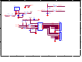
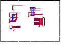
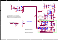
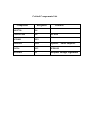
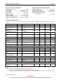
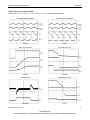
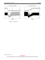
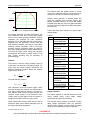
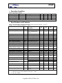
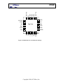
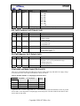
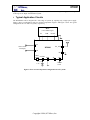
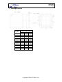
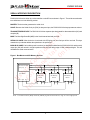
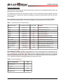
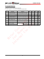
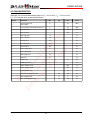
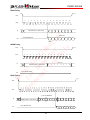
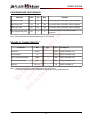
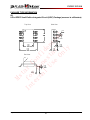
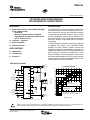
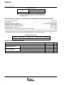
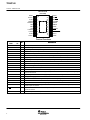
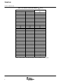
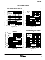
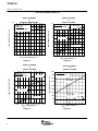
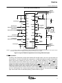
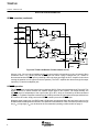
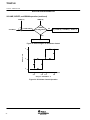
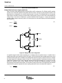
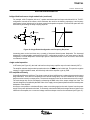
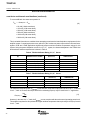
Alpha & Omega Semiconductor
Table 1.
Vo (V)
R1 (kΩ)
R2 (kΩ)
0.8
1.0
open
1.2
4.99
10
1.5
10
11.5
1.8
12.7
10.2
2.5
21.5
10
3.3
31.1
10
5.0
52.3
10
Combination of R1 and R2 should be large enough
to avoid drawing excessive current from the output,
which will cause power loss.
Since the switch duty cycle can be as high as 100%,
the maximum output voltage can be set as high as
the input voltage minus the voltage drop on upper
PMOS and inductor.
Protection Features
The AOZ1041 has multiple protection features to
prevent system circuit damage under abnormal
conditions.
Over Current Protection (OCP)
The sensed inductor current signal is also used for
over current protection. Since the AOZ1041
employs peak current mode control, the COMP pin
voltage is proportional to the peak inductor current.
The COMP pin voltage is limited to be between
0.4V and 2.5V internally. The peak inductor current
is automatically limited cycle by cycle.
When the output is shorted to ground under fault
conditions, the inductor current decays very slow
during a switching cycle because of Vo=0V. To
prevent catastrophic failure, a secondary current
limit is designed inside the AOZ1041. The
measured inductor current is compared against a
preset voltage which represents the current limit,
between 2.5A and 3.6A. When the output current is
more than current limit, the high side switch will be
turned off and EN pin will be pulled down. The
converter will initiate a soft start once the overcurrent condition disappears.
Power-On Reset (POR)
A power-on reset circuit monitors the input voltage.
When the input voltage exceeds 4V, the converter
starts operation. When input voltage falls below
3.7V, the converter will be shut down.
AOZ1041
Thermal Protection
An internal temperature sensor monitors the
junction temperature. It shuts down the internal
control circuit and high side PMOS if the junction
temperature exceeds 155ºC. The regulator will
restart automatically under the control of soft-start
circuit when the junction temperature decreases to
100ºC.
Application Information
The basic AOZ1041 application circuit is show in
Figure 1. Component selection is explained below.
Input capacitor
The input capacitor must be connected to the VIN
pin and PGND pin of the AOZ1041 to maintain
steady input voltage and filter out the pulsing input
current. The voltage rating of input capacitor must
be greater than maximum input voltage plus ripple
voltage.
The input ripple voltage can be approximated by
equation below:
∆VIN =
IO
V
V
× (1 − O ) × O
f × C IN
VIN
VIN
Since the input current is discontinuous in a buck
converter, the current stress on the input capacitor
is another concern when selecting the capacitor.
For a buck circuit, the RMS value of input capacitor
current can be calculated by:
I CIN _ RMS = I O ×
VO
V
(1 − O )
VIN
VIN
if we let m equal the conversion ratio:
VO
=m
VIN
The relation between the input capacitor RMS
current and voltage conversion ratio is calculated
and shown in Fig. 2 below. It can be seen that when
VO is half of VIN, CIN is under the worst current
stress. The worst current stress on CIN is 0.5·IO.
AOZ1041 Datasheet Rev 0.4
CONFIDENTIAL
Not to be distributed or copied without the written permission of Alpha & Omega Semiconductor
8