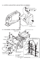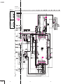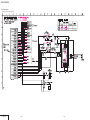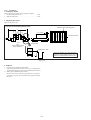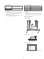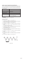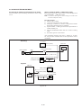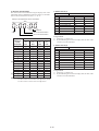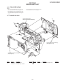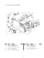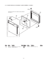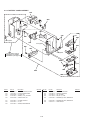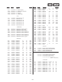
1
CCD-CR1/CR1E SERVICE MANUAL US Model Canadian Model CCD-CR1 AEP Model UK Model E Model Ver 1.0 1998. 08 CCD-CR1E SPECIFICATIONS VIDEO CAMERA RECORDER MICROFILM SAFETY-RELATED COMPONENT WARNING!! COMPONENTS IDENTIFIED BY MARK ! OR DOTTED LINE WITH MARK ! ON THE SCHEMATIC DIAGRAMS AND IN THE PARTS LIST ARE CRITICAL TO SAFE OPERATION. REPLACE THESE COMPONENTS WITH SONY PARTS WHOSE PART NUMBERS APPEAR AS SHOWN IN THIS MANUAL OR IN SUPPLEMENTS PUBLISHED BY SONY. ATTENTION AU COMPOSANT AYANT RAPPORT À LA SÉCURITÉ! LES COMPOSANTS IDENTIFÉS PAR UNE MARQUE ! SUR LES DIAGRAMMES SCHÉMATIQUES ET LA LISTE DES PIÈCES SONT CRITIQUES POUR LA SÉCURITÉ DE FONCTIONNEMENT. NE REMPLACER CES COMPOSANTS QUE PAR DES PIÈSES SONY DONT LES NUMÉROS SONT DONNÉS DANS CE MANUEL OU DANS LES SUPPÉMENTS PUBLIÉS PAR SONY. SAFETY CHECK-OUT After correcting the original service problem, perform the following safety checks before releasing the set to the customer. 1. 2. 3. Check the area of your repair for unsoldered or poorly-soldered connections. Check the entire board surface for solder splashes and bridges. Check the interboard wiring to ensure that no wires are "pinched" or contact high-wattage resistors. Look for unauthorized replacement parts, particularly transistors, that were installed during a previous repair. Point them out to the customer and recommend their replacement. 4. Look for parts which, through functioning, show obvious signs of deterioration. Point them out to the customer and recommend their replacement. 5. Check the B+ voltage to see it is at the values specified. 6. Flexible Circuit Board Repairing • Keep the temperature of the soldering iron around 270˚C during repairing. • Do not touch the soldering iron on the same conductor of the circuit board (within 3 times). • Be careful not to apply force on the conductor when soldering or unsoldering. —2— TABLE OF CONTENTS SERVICE NOTE 1. • VC-205 (Timing Generator)(1/8) Schematic Diagram ....................................... 4-18 • VC-205 (Y/C Processor)(2/8) Schematic Diagram ....................................... 4-21 • VC-205 (REC/PB Head AMP)(3/8) Schematic Diagram ....................................... 4-24 • VC-205 (D/A Converter)(4/8) Schematic Diagram ....................................... 4-27 • VC-205 (Mode Control)(5/8) Schematic Diagram ....................................... 4-30 • VC-205 (Servo/System Control)(6/8) Schematic Diagram ....................................... 4-33 • VC-205 (Servo)(7/8) Schematic Diagram ....................................... 4-36 • VC-205 (Drum/Reel PWM Drive)(8/8) Schematic Diagram ....................................... 4-39 • MJ-88 (Audio REC/PB AMP) Printed Wiring Board .................................... 4-42 • MJ-88 (Audio REC/PB AMP) Schematic Diagram ....................................... 4-45 • PD-99 (RGB Decoder)(1/3) Schematic Diagram ....................................... 4-49 • PD-99 (Timing Generator)(2/3) Schematic Diagram ....................................... 4-51 • PD-99 (SP Audio AMP)(3/3) Schematic Diagram ...................................... 4-53 • PD-99 (RGB Decoder, Timing Generator, SP Audio AMP) Printed Wiring Board .................................... 4-55 • Control Switch Block (FK) Schematic Diagram ........ 4-57 Power Supply During Repairs ............................................ 5 SELF-DIAGNOSIS FUNCTION 1. 2. 3. Self-Diagnosis Function ..................................................... 6 Self-Diagnosis Display ....................................................... 6 Self-Diagnosis Code Table ................................................. 6 1. GENERAL Before you begin ....................................................................... 1-1 Identifying the parts ................................................................... 1-1 Getting started Inserting the batteries ............................................................. 1-2 Using house current ............................................................... 1-3 Charging the battery pack ...................................................... 1-3 Shooting Camera recording ................................................................... 1-3 Photo recording ...................................................................... 1-4 Advanced operations ............................................................. 1-4 Playing back Playing back .......................................................................... 1-5 Watching on a TV screen ....................................................... 1-6 Editing Editing onto another tape ....................................................... 1-6 Additional information Resetting the date and time .................................................... 1-6 Tips for using batteries .......................................................... 1-7 Precautions ............................................................................. 1-8 Trouble check ........................................................................ 1-8 Warning indicators ................................................................. 1-9 Self-diagnosis display ............................................................ 1-9 Using your camcorder abroad ................................................ 1-9 2. DISASSEMBLY 2-1. 2-2. 2-3. 2-4. 2-5. 2-6. 2-7. 2-8. Cabinet (Rear), Cabinet (Front) Assemblies ................... 2-1 VC-205 Board ................................................................. 2-2 Cabinet (Upper), Lens Unit, CD-191 Board ................... 2-3 Battery Case (Battery Case, Battery Lid Assembly) ....... 2-4 PD-99 Board, LCD Panel Assembly ............................... 2-4 LCD Panel ....................................................................... 2-5 MJ-88 Board, MIC .......................................................... 2-5 Service Position-1 (Mainly for Adjustment, Check or Voltage Measurement-1) .................................. 2-6 2-9. Service Position-2 (for Voltage Measurement-2) ............ 2-7 2-10. Circuit Boards Location .................................................. 2-8 3. BLOCK DIAGRAMS 3-1. 3-2. 3-3. 3-4. 3-5. 3-6. 3-7. 3-8. Overall Block Diagram ................................................... 3-1 Camera/Video Block Diagram ........................................ 3-5 VTR/Camera Control Block Diagram ............................. 3-9 Servo Block Diagram .................................................... 3-13 Mode Control Block Diagram ....................................... 3-17 Audio Block Diagram ................................................... 3-19 LCD Block Diagram ..................................................... 3-21 Power Block Diagram ................................................... 3-26 4. PRINTED WIRING BOARDS AND SCHEMATIC DIAGRAMS 4-1. Frame Schematic Diagram .............................................. 4-1 4-2. Printed Wiring Boards and Schematic Diagrams ............ 4-4 • CD-191 (CCD Imager) Printed Wiring Board .............. 4-5 • CD-191 (CCD Imager) Schematic Diagram ................. 4-7 • VC-205 (Timing Generator, Y/C Processor, REC/PB Head AMP, D/A Converter, Mode Control, Servo/System Control, Servo, Drum/Reel PWM Drive) Printed Wiring Board .................................... 4-10 5. ADJUSTMENTS 5-1. Camera Section Adjustment ............................................ 5-1 1-1. Preparations before Adjustment (Camera Section) ......... 5-1 1-1-1. List of Service Tools ........................................................ 5-1 1-1-2. Preparations .................................................................... 5-2 1-1-3. Precaution ........................................................................ 5-4 1. Setting the Switch ............................................................ 5-4 2. Adjusting Procedure ........................................................ 5-4 3. Subjects ........................................................................... 5-4 1-2. Initialization of D, E, F Page Data .................................. 5-5 1. Initializing the D,E,F Page Data ...................................... 5-5 2. Modification of D, E, F Page Data .................................. 5-5 3. D Page Table .................................................................... 5-5 4. F Page Table .................................................................... 5-6 5. E Page Table .................................................................... 5-9 1-3. Camera System Adjustments ......................................... 5-12 1. HALL Adjustment ......................................................... 5-12 2. Flange Back Check ........................................................ 5-13 3. Picture Frame Setting .................................................... 5-13 4. Color Reproduction Adjustment .................................... 5-14 5. Iris In/Out Adjustment .................................................. 5-15 6. Max Gain Adjustment ................................................... 5-15 7. Auto White Balance Standard Data Input ..................... 5-16 8. Auto White Balance Adjustment ................................... 5-16 9. White Balance Check .................................................... 5-17 1-4. LCD System Adjustment ............................................... 5-18 1. LCD Initial Data Input .................................................. 5-18 2. VCO Adjustment (PD-99 Board) .................................. 5-19 3. D Range Adjustment (PD-99 Board) ............................. 5-19 4. Bright Adjustment (PD-99 Board) ................................ 5-20 5. Contrast Adjustment (PD-99 Board) ............................. 5-20 6. V-COM Level Adjustment (PD-99 Board) .................... 5-21 7. Color Adjustment (PD-99 board) .................................. 5-21 8. V-COM Adjustment (PD-99 board) .............................. 5-22 9. White Balance Adjustment ............................................ 5-22 9-1. Panel VR Adjustment (PD-99 board) ............................ 5-22 —3— 9-2. Panel VB Adjustment (PD-99 Board) ........................... 5-23 10. Bright Check/Adjustment (PD-99 Board) ..................... 5-23 5-2. Video Section Adjustments ........................................... 5-24 2-1. Preparations before Adjustment .................................... 5-24 2-1-1. Equipment to Be Used .................................................. 5-24 2-1-2. Precautions on Adjusting .............................................. 5-25 2-1-3. Adjusting Connectors .................................................... 5-25 2-1-4. Connecting the Equipment ............................................ 5-26 2-1-5. Output Level and Impedance ........................................ 5-26 2-2. System Control System Adjustment .............................. 5-27 1. Initialization of D, E, F Page Data ................................ 5-27 2. Dry Battery Down Data Check (VC-205 Board) .......... 5-27 2-3. Video System Adjustments ............................................ 5-27 1. 28 MHz Origin Oscillation Adjustment (VC-205 Board) ............................................................. 5-27 2. AFC f0 Adjustment (VC-205 Board) ............................. 5-28 3. Y Out Level Adjustment (VC-205 Board) .................... 5-28 4. C Out Level Adjustment (VC-205 Board) ..................... 5-29 5. RP Filter f0 Adjustment (VC-205 Board) ...................... 5-30 6. REC Y Current Adjustment (VC-205 Board) ................ 5-31 7. REC L Level Adjustment (VC-205 Board) ................... 5-31 8. REC C Current Adjustment (VC-205 Board) ................ 5-32 2-4. Audio System Adjustment ............................................. 5-33 1. 1.5 MHz Deviation Adjustment (MJ-88 Board) ............ 5-34 2. BPF Adjustment (MJ-88 Board) .................................... 5-34 3. Overall Level Characteristics Check ............................. 5-34 4. Overall Distortion Check ............................................... 5-34 5. Overall Noise Level Check ............................................ 5-34 5-3. Service Mode ................................................................. 5-39 3-1. Adjustment Remote Commander .................................. 5-39 1. Using the Adjustment Remote Commander .................. 5-39 2. Precautions Upon Using the Adjustment Remote Commander ............................ 5-39 3-2. Data Process .................................................................. 5-40 3-3. Service Mode ................................................................. 5-41 1. Setting the Test Mode .................................................... 5-41 2. Video Cartridge Emergence Memory Address .............. 5-41 2-1. EMG Code (Emergency Code) ..................................... 5-41 2-2. Position SW Code ......................................................... 5-41 3. Record of Use of the Video Cartridge ........................... 5-42 4. Bit Value Discrimination ............................................... 5-43 5. Switch Check (1) ........................................................... 5-43 6. Switch Check (2) ........................................................... 5-43 7. Switch Check (3) ........................................................... 5-44 6. REPAIR PARTS LIST 6-1. Exploded Views ............................................................... 6-1 6-1-1. Cabinet Section ................................................................ 6-1 6-1-2. Frame Assembly, Lens Unit ............................................ 6-2 6-1-3. Cabinet (Front) Block Assembly ..................................... 6-3 6-1-4. Cabinet (Rear) Block Assembly-1 (Cabinet (Rear) Assembly, PD-99 Board) ................................................. 6-4 6-1-5. Cabinet (Rear) Block Assembly-2 (Hinge Assembly, LCD Panel) ........................................ 6-5 6-1-6. Battery Case Assembly .................................................... 6-6 6-2. Electrical Parts List ......................................................... 6-7 * The color reproduction frame is shown on page 173. —4— SERVICE NOTE 1. POWER SUPPLY DURING REPAIRS In this unit, about 5 seconds after power is supplied (4.2V) to the battery terminal using a regulated power supply, the power is shut off so that the unit cannot operate. This following three methods are available to prevent this. Take note of which to use during repairs. Method 1. Decrease the voltage to 3Vdc. Method 2. Connect the servicing remote commander RM-95 (J-6082-053-B), and set the remote commander switch to the “ADJ” side. Method 3. Use the AC power adaptor. —5— SELF-DIAGNOSIS FUNCTION 1. 2. SELF-DIAGNOSIS FUNCTION When problems occur while the unit is operating, the self-diagnosis function starts working, and displays on the LCD display what to do. This function consists of two display; self-diagnosis display and service mode display. Details of the self-diagnosis functions are provided in the Instruction manual. SELF-DIAGNOSIS DISPLAY When problems occur while the unit is operating, the counter of the LCD display consists of an alphabet and 4-digit numbers, which blinks at 3.2 Hz. This 5-character display indicates the “repaired by:”, “block” in which the problem occurred, and “detailed code” of the problem. LCD display C:31:11 Blinks at 3.2Hz C 11 Block Repaired by: C : Corrected by customer H : Corrected by dealer E : Corrected by service engineer 3. 31 Detailed Code Refer to Indicates the appropriate "3. Self-diagnosis Code Table". step to be taken. E.g. 31 • Reload the video cartridge. 32 • Turn on power again. • After leaving the machine as it is for about one hour, perform operations from the beginning. SELF-DIAGNOSIS CODE TABLE Repaired by: Self-diagnosis Code C C C C Block Detailed Function Code 1 2 2 2 2 3 3 1 3 2 8 0 0 0 0 0 Symptom/State Correction Format of the video cartridge is different. Use the video cartridge of correct format. Video head is dirty. Non-standard battery is used. Use the InfoLITHIUM battery. • Load the video cartridge again, and perform operations from the beginning. • Remove the battery or power cable, connect, and perform operations from the beginning. • After leaving the machine as it is for about one hour, perform operations from the beginning. —6— SECTION 1 GENERAL 1-1 CCD-CD1/CR1E This section is extracted from instruction manual. (CCD-CR1E) 1-2 1-3 1-4 1-5 1-6 1-7 1-8 1-9E CCD-CR1/CR1E SECTION 2 DISASSEMBLY The following flow chart shows the disassembly procedure. CCD-CR1/CR1E Video camera 2-7. MJ-88 board 1-5 2-1. Cabinet (front) assembly 1-8 2-7. Mic 6-7 2-5. PD-99 board 1-5 2-1. Cabinet (rear) assembly 9-!¡ 2-5. Speaker 6-7 2-2. VC-205 board 2-5. Hinge (LCD assembly) 8-!∞ 2-3. Cabinet (upper) 1-2 2-3. Iris assy 7,8 2-3. Lens unit 3,4 2-3. CD-191 board 5,6 2-6. LCD panel 2-4. Battery assembly NOTE: Follow the disassembly procedure in the numerical order given. 2-1. CABINET (REAR), CABINET (FRONT) ASSEMBLIES 1—8 Cabinet (front) disassembly removal 9—!¡ Cabinet (rear) disassembly removal 1 Remove the video cartridge from the CCD-CR1/CR1E 2 Screw (M1.4 × 2.5) !¡ Cabinet (rear) assembly 6 Screws (M1.4 × 3) 9 Close the battery case a 5 Open the battery case. !º FP-686 flexible board (CN401 33P of VC-205 board) 7 MJ-88 board CN151 30P of VC-205 board 6 Screw (M1.4 × 3) a b 2 Screws (M1.4 × 3) 3 Open the jack lid assembly it in the direction of the arrow. 8 Cabinet (front) assembly 4 Screw (M1.4 × 3) 2-1 b 2-2. VC-205 BOARD 6 FP-685 flexible board CN801 20P (VC-205 board) 3 1 -19 CDARD BO 4 2 4 3 Remove the two claws 5 -20 VC ARD BO Claw of shield 5 VC-205 board 1 Control switch block CN601 15P (VC-205 board) 2 CD-191 board CN501 30P (VC-205 board) 2-2 To assemble it, insert the claw of the shield case into the cut-out of the plate spring. Cut out of plate spring 2-3. CABINET (UPPER), LENS UNIT, CD-191 BOARD 2 !¡ Base plate Cabinet (upper) 1 Disengage the claw. To assemble, align the head of the control shaft with the groove of the ZOOM knob. !º Tapping screws (M1.7 × 3) 3 Tapping screw (M1.7 × 4) 6 CD-191 board 5 Tapping screws (B1.7 × 6) CD Bo -1 ar 91 d 4 9 Screws, lock ace (M1.7 × 1.6) 1—2 Cabinet (upper) 3, 4 Lens unit 5, 6 CD-191 board 7, 8 Iris assy Lens unit 7 Screw (P1.7 × 3.5) 8 Iris assy 3 Tapping screw (M1.7 × 4) ZOOM disk Control pulley 2-3 To assemble, align the pin of the control pulley with the groove of the ZOOM disk of the lens unit. 2-4. BATTERY CASE (BATTERY CASE, BATTERY LID ASSEMBLY) 1 Remove the BT flexible cover to the direction of arrow. Move while it is warped and swayed. 2 BT case shaft 2-5. PD-99 BOARD, LCD PANEL ASSEMBLY 3 Battery case terminal !£ Open the hinge to one side. !™ Screw, lock ace (M1.7 × 1.4) !∞ !¡ 9 !º Tapping screws (M1.7 × 3) !¢ 7 Be careful not to tighten up excessively. 8 Remove the spring. !™ Screws, lock ace (M1.7 × 1.4) 1 Peel off the insulation sheet. 2 4 Screw (M1.4 × 2.5) 3 7 PD BO-99 AR D 5 4 5 6 While peeling off the sheet, remove the speaker. 2 FP-686 flexible board CN701 3 Speaker connector 4 Screw (M1.4 × 2.5) 1—5 PD-99 board 6, 7 Speaker 8—!∞ Hinge 1—8 Hinge disassembling and re-assembling 2-4 6 1 Route the flexible board coming from the LCD through. Assembling the hinge 8 1 Screws (M1.4 × 2) 2-6. LCD PANEL 3 LCD panel 2 Be carefull not to rotate over 180˚ 2 1 Screws (M1.4 × 2) 4 Spacer panel 2-7. MJ-88 BOARD, MIC MIC1 Microphone retainer 7 5 4 Screws (M1.4 × 2) 6 Screws (M1.4 × 2) 3 1—5 MJ-88 board 6, 7 MIC MJ-88 board cable 2 Screw (M1.4 × 2) 1 MIC CN753 2P 2-5 2-8. SERVICE POSITION-1 (Mainly for adjustment, check or voltage measurement-1) Firstly, remove the following parts referring DISASSEMBLY (sections 2-1 and 2-7), and connect parts as shown below. Regulated DC power supply (DC +3 V) Power supply cord jig (J-6082-415-A) VC-205 board (CN801) Fully close the battery case. CD-191 board Lens unit 5 -20 VC ARD BO MJ-88 board Adjustment remote commander RM-95 CPC 11 jig (J-6082-425-A) VC-205 board (CN152) Regulated DC power supply (DC +5 V) Cabinet (rear) assembly 2-6 2-9. SERVICE POSITION-2 (For voltage measurement-2) Firstly, remove the following parts referring DISASSEMBLY (sections 2-1, 2-2, 2-3, and 2-7), and connect parts as shown below. Regulated DC power supply (DC +3 V) Fix the battery case OPEN/CLOSE sensor switch to the "ON" position with adhesive tape. Power supply cord jig (J-6082-415-A) VC-205 board (CN801) POWER ON/OFF switch Cabinet (upper) assembly VC-205 board Cartridge CD-191 board MJ-88 board Extension jig (J-6082-426-A) VC-205 board (CN101) Cabinet (rear) assembly 2-7 2-10.CIRCUIT BOARDS LOCATION FP-685 (VC-205—BATTERY TERMINAL CONNECTOR) CONTROL SWITCH BLOCK CD-191 (CCD IMAGER) MJ-88 (AUDIO REC/PB AMP) VC-205 TIMING GENERATOR, Y/C PROCESSOR, REC/PB HEAD AMP, D/A CONVERTER, MODE CONTROL, SERVO/SYSTEM CONTROL, SERVO, DRUM/REEL PWM DRIVE PD-99 RGB DRIVER, TIMING GENERATOR, SP AUDIO AMP LCD PANEL FP-686 (PD-99—VC-205 CONNECTOR) 2-8E CCD-CR1/CR1E SECTION 3 BLOCK DIAGRAMS 3-1. OVERALL BLOCK DIAGRAM 3-1 3-2 3-3 3-4 CCD-CR1/CR1E 3-2. CAMERA/VIDEO BLOCK DIAGRAM IC101 1 REC IC951 7 REC 0.1µsec/div 0.3Vp-p IC502 @§ REC H 0.5Vp-p 0.7Vp-p H IC501 !¡,!™ REC/PB IC951 1, 2 REC Q201 B PB 7Vp-p 14.187MHz 3.0Vp-p 0.3Vp-p H H IC501 5 REC/PB Q0001 C REC IC502 2 – !¡ REC IC951 3, 4 REC 7Vp-p 3.2Vp-p 28.375MHz (PAL) 28.635MHz (NTSC) Q0014 E PB 1Vp-p 8Vp-p 0.1µsec 0.14µsec H 0.17µsec 0.7Vp-p R227 REC/PB IC151 4 REC/PB Q204 E REC/PB 0.7Vp-p H 0.5Vp-p H 1.0Vp-p H R230 REC/PB IC151 7 REC/PB IC151 2 REC/PB H 0.5Vp-p R232 REC/PB 2.0Vp-p H 1.0Vp-p H 0.1Vp-p H R220 REC/PB H 3-5 0.2Vp-p 3-6 3-7 3-8 CCD-CR1/CR1E 3-3. VTR/CAMERA CONTROL BLOCK DIAGRAM IC402 1 REC/PB 20MHz 3-9 1.5Vp-p 3-10 3-11 CCD-CR1/CR1E CCD-CR1/CR1E 3-4. SERVO BLOCK DIAGRAM IC452 1,2,@ª 1.2Vp-p 5.5msec IC451 5,7,9 REC/PB 0.4Vp-p 40msec 3-13 3-14 3-15 3-16 CCD-CR1/CR1E 3-5. MODE CONTROL BLOCK DIAGRAM IC604 $º REC/PB 20MHz 3.2Vp-p IC605 3 REC/PB 32.768kHz 3-17 1.1Vp-p 3-18 CCD-CR1/CR1E 3-6. AUDIO BLOCK DIAGRAM 3-19 3-20 CCD-CR1/CR1E 3-7. LCD BLOCK DIAGRAM IC5502 @º REC/PB 4Vp-p H IC5502 @™ REC/PB 4Vp-p IC5502 8 REC/PB H 0.5Vp-p H IC5502 9 REC/PB 0.2Vp-p H IC5502 !º REC/PB H 0.1Vp-p IC5502 @¢ REC/PB 4Vp-p H IC5601 #¶ REC/PB 2.8Vp-p H IC5601 #¢ REC/PB V 3-21 3-22 2.8Vp-p 3-23 3-24 CCD-CR1/CR1E CCD-CR1/CR1E 3-8. POWER BLOCK DIAGRAM IC801 3 REC/PB 0.7Vp-p 2.5µsec 3-26 3-27 3-28E CCD-CR1/CR1E SECTION 4 PRINTED WIRING BOARDS AND SCHEMATIC DIAGRAMS 4-1. FRAME SCHEMATIC DIAGRAM 4-1 4-2 4-3 FRAME SCHEMATIC DIAGRAM CCD-CR1/CR1E CD-191 (CCD IMAGER) PRINTED WIRING BOARD — Ref. No. CD-191 Board; 1,000 Series — 4-2. PRINTED WIRING BOARDS AND SCHEMATIC DIAGRAMS CD-191 BOARD THIS NOTE IS COMMON FOR WIRING BOARDS AND SCHEMATIC DIAGRAMS (In addition to this, the necessary note is printed in each block) (Measuring conditions voltage and waveform) (For printed wiring boards) • b: Pattern from the side which enables seeing. (The other layers' patterns are not indicated.) • Through hole is omitted. • Circled numbers refer to waveforms. • There are few cases that the par t printed on diagram isn’t mounted in this model. • Chip parts. Transistor Diode 12 3 32 1 4 5 32 1 1 3 2 54 3 2 3 1 2 3 1 2 CN951 A-1 CN952 D-4 Pattern box 1 Approx. 90 cm IC951 IC952 B-3 B-3 L951 L952 D-4 B-2 R951 R952 R953 R955 R956 R957 R958 R959 B-3 B-3 B-3 B-3 C-4 C-4 C-4 B-3 2. Adjust the distance so that the output waveform of Fig. a and the Fig. b can be obtain. Yellow Temperature characteristics External dimensions (mm) • Constants of resistors, capacitors, ICs and etc with XX indicate that they are not used. In such cases, the unused circuits may be indicated. • All variable and adjustable resistors have characteristic curve B, unless otherwise noted. • Signal name XEDIT → EDIT PB/XREC → PB/REC • 2 : non flammable resistor • 1 : fusible resistor • C : panel designation • A : B+ Line • B : B– Line •J : IN/OUT direction of (+,–) B LINE. • C : adjustment for repair. • Circled numbers refer to waveforms. A B H A=B B A Fig. a (Video output terminal output waveform) Yellow Cyan Green White Magenta Red Blue Electron beam scanned frame The components identified by mark ! or dotted line with mark ! are critical for safety. Replace only with part number specified. CRT picture frame For printed wiring board • This board is six-layer print board. However, the patterns of layers two to five have not been included in the diagram. Fig.b (Picture on monitor TV) When indicating parts by reference number, pleas include the board name. FP-685 (VC-205—BATTERY TERMINAL CONNECTOR) CONTROL SWITCH BLOCK CD-191 (CCD IMAGER) MJ-88 (AUDIO REC/PB AMP) VC-205 TIMING GENERATOR, Y/C PROCESSOR, REC/PB HEAD AMP, D/A CONVERTER, MODE CONTROL, SERVO/SYSTEM CONTROL, SERVO, DRUM/REEL PWM DRIVE CD-191 C-4 Front of the lens Kinds of capacitor CCD IMAGER D951 1. Connection (For schematic diagrams) • All capacitors are in mF unless otherwise noted. pF : m mF. 50V or less are not indicated except for electrolytics and tantalums. • Chip resistors are 1/10W unless otherwise noted. kW=1000W, MW=1000kW. • Caution when replacing chip parts. New parts must be attached after removal of chip. Be careful not to heat the minus side of tantalum capacitor, Because it is damaged by the heat. • Some chip part will be indicated as follows. Example C541 L452 22U 10UH TA A 2520 Note : B-3 C-3 B-4 C-3 B-3 B-3 C-3 B-3 C-4 Red Blue E 45 6 White Magenta B 65 4 • Voltages and waveforms are measured between the measurement points and ground when camera shoots color bar chart of pattern box. They are reference values and reference waveforms. (VOM of DC 10 MW input impedance is used.). • Voltage values change depending upon input impedance of VOM used.) Cyan Green C C951 C952 C953 C954 C955 C956 C957 C958 C959 4-4 There are few cases that the part printed on this diagram isn’t mounted in this model. Precautions Upon Replacing CCD Imager • The CD-191 board mounted as a repair part is not equipped with a CCD imager. When replacing this board, remove the CCD imager from the old one and mount it onto the new one. • If the CCD imager has been replaced, carry out all the adjustments for the camera section. • As the CCD imager may be damaged by static electricity from its structure, handle it carefully like for the MOS IC. In addition, ensure that the receiver is not covered with dusts nor exposed to strong light. 4-5 4-6 CCD-CR1/CR1E CD-191 BOARD 1 IC951 1, 2 REC 7Vp-p H 2 IC951 3, 4 REC 7Vp-p H 3 IC951 7 REC H 4-7 4-8 0.5Vp-p CCD IMAGER CD-191 CCD-CR1/CR1E CCD-CR1/CR1E VC-205 (TIMING GENERATOR, Y/C PROCESSOR, REC/PB HEAD AMP, D/A CONVERTER, MODE CONTROL, SERVO/SYSTEM CONTROL, SERVO, DRUM/REEL PWM DRIVE) PRINTED WIRING BOARD — Ref. No. VC-205 Board; 10,000 Series — VC-205 BOARD (SIDE A) C157 C201 C202 C204 C206 C207 C208 C209 C210 C211 C212 C217 C218 C219 C225 C226 C229 C231 C237 C239 C241 C250 C401 C402 C403 C404 C405 C406 C407 C408 C409 C410 C411 C412 C413 C414 C451 C452 C453 C454 C455 C456 C457 C458 C459 C460 C461 C462 C463 C464 C465 C466 C467 C468 C469 C470 C471 C472 C473 C474 C475 C476 C477 C479 C480 C481 C482 C483 C484 C485 C486 C501 C502 C503 C506 C508 C509 C510 C511 C514 C515 C518 C531 C561 C562 MAIN BOARD VC-205 B-8 D-3 D-2 D-3 D-3 D-3 D-3 D-4 D-4 D-2 D-2 D-3 D-3 D-3 D-3 D-2 D-4 D-4 D-3 C-3 C-3 D-3 B-4 B-3 B-3 B-3 B-4 A-4 A-4 A-4 A-5 B-4 A-5 B-3 A-4 A-4 B-7 B-7 B-7 B-7 B-7 B-7 B-6 B-6 B-7 A-7 A-7 B-6 A-7 A-6 A-6 A-6 A-7 A-6 A-7 A-7 A-6 A-7 A-7 A-7 A-6 A-6 A-5 A-6 A-6 A-6 A-6 A-6 A-6 B-5 A-6 D-5 D-5 D-5 D-6 D-5 D-6 D-5 D-6 D-5 D-5 D-5 D-4 D-6 D-6 C565 C570 C571 C572 C573 C807 C808 C810 C813 C843 C844 C845 C846 C847 C848 C849 C0016 C0017 C0018 C0019 C0020 C0021 C0022 C0023 C0024 C0025 C0029 C0030 C0032 C0034 C0035 C0036 C0037 C0038 C0042 C0043 C0051 C0052 C0061 C0063 D-6 D-6 D-6 D-6 D-6 D-1 D-1 D-1 B-1 D-2 D-2 C-2 D-2 D-2 D-2 D-2 B-5 C-5 B-5 B-5 B-5 B-5 B-5 C-5 C-5 C-5 B-5 B-5 B-5 B-4 B-5 C-4 B-4 C-4 B-4 B-4 C-4 C-4 C-4 C-5 CN152 A-8 CN801 D-1 CN0101 C-6 D451 D502 D201 D801 D802 D803 A-6 D-5 D-3 C-1 B-1 C-1 F801 D-1 FB001 FB002 FB201 FB203 FB401 FB501 FB503 FB504 FB505 FB801 FB802 FB803 FB806 B-5 C-5 C-3 C-3 B-4 D-5 D-5 D-5 D-5 D-2 C-2 D-2 D-2 IC202 IC401 IC402 IC451 IC452 IC453 IC501 IC0101 D-3 A-5 A-3 B-7 A-7 A-5 D-5 B-5 L201 L202 L203 L204 L205 L207 L209 L501 D-2 C-4 C-4 D-3 D-4 C-3 C-3 D-4 4-10 L554 L555 L804 L805 L806 L807 L808 L809 L810 L811 L812 L813 L814 L0001 L0002 L0003 L0004 L0005 L0007 L0009 L0010 L0012 L0013 L0014 L0015 L0018 L0019 L0020 L0021 L0022 D-6 D-6 B-2 B-2 C-2 A-2 A-2 B-2 C-2 B-2 D-2 D-2 D-2 C-5 C-5 B-5 C-5 B-4 B-4 C-4 C-4 C-4 C-4 C-5 C-5 C-4 C-5 C-4 C-4 C-5 Q201 Q202 Q203 Q204 Q208 Q401 Q451 Q452 Q453 Q553 D-3 D-2 D-2 D-4 D-4 B-4 A-6 A-6 B-5 D-6 R202 R203 R204 R205 R206 R207 R208 R209 R210 R211 R212 R215 R216 R223 R224 R226 R233 R234 R236 R237 R238 R239 R240 R241 R242 R243 R245 R247 R248 R249 R251 R252 R253 R256 R257 R401 R402 R403 R404 R405 R406 R407 R408 D-2 D-3 D-2 D-2 D-3 D-3 D-2 D-3 D-2 D-2 D-4 D-4 D-4 D-3 D-2 D-3 D-4 D-4 D-4 D-4 D-3 D-3 D-3 D-4 D-3 D-3 D-3 D-2 D-2 D-2 D-3 D-3 C-3 C-4 C-3 B-3 B-3 A-5 A-4 A-4 A-4 A-4 A-4 R409 R410 R411 R412 R413 R414 R415 R416 R417 R418 R419 R420 R421 R426 R427 R428 R429 R430 R431 R432 R433 R434 R435 R436 R451 R452 R453 R454 R455 R456 R457 R458 R459 R460 R461 R462 R463 R464 R465 R466 R467 R468 R469 R470 R471 R472 R473 R474 R475 R476 R477 R478 R479 R480 R484 R502 R503 R504 R506 R508 R510 R511 R512 R527 R570 R571 R572 R573 R578 R882 R0023 R0024 R0049 R0069 R0088 C-4 B-4 B-4 B-4 B-4 A-4 A-4 A-4 A-4 A-4 A-4 A-4 A-4 A-4 A-4 B-4 B-4 A-4 A-4 B-3 B-4 B-4 B-4 B-4 B-7 B-7 B-7 B-7 B-6 B-7 B-7 B-7 B-7 A-7 B-7 B-7 A-6 A-6 A-6 A-5 A-6 A-6 A-6 A-6 A-6 A-6 A-6 A-6 A-6 A-6 A-6 B-5 A-5 B-6 A-6 D-5 D-5 D-6 D-6 D-5 D-5 D-5 D-5 D-5 D-6 D-6 D-6 D-6 D-6 C-2 B-5 B-5 C-4 C-4 C-4 T801 T802 B-1 B-1 X401 X501 X602 B-3 D-5 A-7 4-11 4-12 CCD-CR1/CR1E CCD-CR1/CR1E VC-205 BOARD (SIDE B) C152 C153 C154 C155 C156 C158 C159 C160 C161 C162 C171 C172 C173 C191 C192 C193 C194 C205 C224 C227 C230 C232 C233 C234 C235 C236 C243 C244 C245 C246 C247 C248 C249 C252 C261 C262 C263 C264 C265 C266 C487 C488 C512 C513 C517 C520 C521 C522 C523 C524 C525 C526 C527 C529 C530 C534 C535 C552 C553 C555 C557 C558 C560 C567 C568 C569 C602 C603 C604 C605 C606 C607 C608 C609 C610 C611 C612 C613 C801 C802 C803 C804 C805 C806 C809 C811 C812 C814 C815 C816 4-13 4-14 C-10 C-10 C-10 C-10 C-10 C-9 C-9 C-10 C-10 C-10 C-10 C-9 C-10 C-10 C-10 B-10 B-11 B-13 D-14 D-13 D-13 D-14 D-13 D-13 D-14 D-14 D-14 D-14 D-14 D-14 D-14 D-14 C-13 D-14 D-13 D-13 D-13 D-13 D-13 D-13 A-10 A-10 D-12 D-12 D-12 D-12 D-12 D-12 D-12 D-12 D-12 D-12 D-12 D-13 D-13 D-12 D-12 D-11 C-11 D-11 C-11 C-11 C-11 D-11 C-11 C-11 D-16 B-13 A-13 A-11 A-11 A-11 A-11 B-13 A-13 A-12 A-11 A-11 D-15 D-15 D-15 D-16 C-16 C-16 D-15 D-15 D-15 D-16 D-15 D-15 C817 C818 C819 C820 C821 C822 C823 C824 C825 C826 C827 C828 C829 C830 C831 C832 C833 C834 C835 C836 C837 C838 C839 C840 C841 C842 C850 C851 C852 C853 C854 C855 C856 C857 C858 C859 C869 C0001 C0002 C0003 C0004 C0005 C0006 C0007 C0008 C0009 C0011 C0012 C0013 C0014 C0026 C0027 C0028 C0031 C0039 C0045 C0046 C0047 C0049 C0053 C0054 C0055 C0056 C0058 C0062 C0066 C0067 C0068 C0069 C0070 C0071 C0072 C0075 C0076 C0081 C0082 C0083 C0084 C0085 C0086 C-16 C-16 D-16 C-15 C-15 C-15 C-16 C-15 C-15 C-15 B-15 C-15 A-15 B-15 B-15 C-15 B-16 A-16 A-15 B-15 C-15 B-15 B-16 B-16 A-16 B-16 B-13 B-14 C-14 A-14 A-14 B-14 A-14 C-14 C-16 D-15 B-14 C-11 C-12 C-11 C-11 D-11 C-11 C-11 C-12 C-12 C-12 C-12 C-12 C-12 B-12 B-12 B-12 B-12 B-13 C-13 C-13 C-13 C-13 C-13 C-12 C-12 C-12 C-13 C-12 D-12 C-13 D-13 D-13 C-12 C-12 C-12 D-12 B-13 D-13 C-13 C-12 D-12 D-12 C-13 CN151 CN401 CN501 CN601 B-10 A-14 D-11 A-13 D202 D551 D601 D602 D-14 D-11 D-16 A-11 4-15 D603 D604 D605 D805 D806 D807 D808 D809 D810 D811 D812 D813 D0001 B-13 A-10 A-11 B-16 B-15 B-15 C-15 B-16 A-16 A-15 A-16 B-16 D-12 FB202 FB205 FB206 FB506 FB601 FB602 D-14 C-14 D-14 D-13 B-13 B-13 IC151 IC152 IC201 IC204 IC502 IC551 IC601 IC602 IC603 IC604 IC605 IC801 C-9 B-10 C-13 D-14 D-12 D-11 D-16 B-13 B-13 A-12 A-11 D-15 L151 L152 L153 L191 L192 L206 L261 L262 L601 L171 C-10 C-10 C-10 C-10 B-11 D-14 D-13 D-13 D-16 C-9 Q152 Q171 Q552 Q601 Q602 Q801 Q802 Q803 Q804 Q805 Q806 Q807 Q808 Q809 Q810 Q811 Q812 Q813 Q814 Q815 Q816 Q817 Q818 Q819 Q820 Q821 Q822 Q823 Q824 Q825 Q826 Q827 Q828 Q829 Q830 Q831 Q832 Q833 Q834 Q835 Q836 Q0001 Q0002 Q0003 Q0004 C-10 C-9 D-11 A-11 A-11 B-16 B-16 B-15 B-15 C-15 A-16 A-15 B-15 A-15 A-15 B-15 C-15 B-14 B-14 A-16 B-14 B-13 B-14 B-14 B-14 A-14 A-14 A-14 A-14 C-14 B-14 B-14 A-14 B-14 B-14 A-14 B-14 B-14 C-14 B-16 C-16 C-11 C-12 C-11 D-11 Q0006 Q0009 Q0014 Q0015 Q0016 Q0018 Q0022 Q0023 Q0024 Q0027 Q0030 Q0032 Q0033 Q0034 Q0035 Q0036 Q0037 Q0038 Q0039 Q0040 Q0041 B-12 B-13 B-13 C-13 C-13 C-13 C-13 C-13 C-13 C-13 C-12 C-12 C-12 C-12 C-12 B-13 C-12 C-12 C-12 C-12 C-12 R153 R155 R156 R157 R158 R160 R171 R172 R173 R174 R217 R220 R227 R228 R229 R230 R232 R244 R246 R250 R261 R271 R272 R422 R423 R424 R425 R481 R482 R483 R507 R509 R529 R558 R559 R560 R561 R562 R563 R564 R565 R566 R567 R568 R569 R574 R575 R576 R577 R601 R602 R603 R604 R605 R606 R607 R608 R609 R610 R611 R612 R613 R614 R615 R616 R617 R618 R619 C-10 C-10 C-10 C-10 C-9 C-9 C-9 C-9 C-9 C-9 C-14 D-14 D-13 D-13 D-13 D-14 D-14 D-14 D-14 D-14 D-13 D-13 D-14 A-13 A-13 A-13 A-13 A-10 A-10 A-10 D-12 D-12 D-12 D-11 D-11 D-11 D-11 D-11 C-11 C-11 D-11 C-11 C-11 C-11 C-11 D-11 C-11 C-11 C-11 A-11 A-11 A-13 A-13 A-13 B-13 B-13 B-13 A-13 A-13 A-13 A-13 B-13 A-13 A-11 B-11 B-11 B-11 B-13 R620 R621 R622 R623 R624 R625 R626 R627 R628 R629 R630 R631 R632 R633 R634 R635 R636 R637 R640 R641 R642 R643 R644 R645 R646 R801 R803 R804 R807 R808 R810 R814 R815 R816 R817 R818 R819 R820 R821 R822 R823 R824 R825 R826 R829 R830 R831 R832 R833 R834 R835 R836 R837 R838 R839 R840 R841 R842 R843 R844 R845 R846 R847 R848 R849 R850 R851 R852 R853 R854 R855 R856 R857 R859 R860 R861 R862 R863 R864 R865 R866 R867 R868 R869 R870 R871 R872 R873 R874 R875 A-11 B-13 B-13 B-13 A-13 A-13 A-13 B-13 B-13 B-13 A-13 A-13 A-11 A-13 A-11 A-11 A-10 B-13 A-13 A-13 A-11 A-11 A-10 B-13 A-11 D-15 D-15 D-15 D-16 D-16 D-16 D-16 D-15 D-16 D-15 D-15 D-15 D-15 D-15 D-15 D-16 D-15 D-15 D-15 D-15 C-15 C-15 D-16 D-15 D-15 D-15 D-15 C-15 D-15 D-15 D-15 D-15 C-16 C-15 C-15 C-15 C-15 B-14 B-14 B-14 B-14 A-16 A-16 B-14 B-14 A-14 A-14 C-14 B-14 B-14 C-14 C-14 C-14 B-14 B-14 B-14 B-14 B-14 B-14 A-14 B-14 B-14 C-14 C-14 C-14 R876 R877 R878 R879 R883 R884 R890 R891 R892 R893 R894 R895 R0001 R0002 R0003 R0004 R0005 R0006 R0007 R0008 R0009 R0010 R0011 R0014 R0015 R0016 R0017 R0018 R0020 R0025 R0026 R0027 R0029 R0030 R0031 R0032 R0033 R0034 R0041 R0044 R0054 R0055 R0056 R0057 R0058 R0060 R0061 R0062 R0065 R0066 R0072 R0073 R0074 R0075 R0076 R0079 R0080 R0085 R0090 R0091 R0093 R0098 R0099 R0100 R0104 R0106 R0108 R0109 R0110 R0112 R0114 R0123 R0124 R0125 R0126 R0127 R0128 R0129 R0130 R0131 R0132 R0133 R0134 R0135 C-14 B-14 B-14 B-14 D-16 D-16 C-16 C-16 B-14 D-16 C-16 B-14 C-12 C-11 C-11 C-12 C-12 C-11 C-12 C-12 C-11 D-12 D-11 B-12 B-12 C-12 C-12 C-12 C-13 C-12 C-12 B-12 B-12 B-12 B-12 B-12 B-12 B-12 B-13 B-13 B-13 B-13 C-13 C-13 C-13 C-13 C-13 C-13 C-13 C-13 C-13 C-13 C-13 C-13 D-13 C-12 C-12 C-12 C-12 C-13 C-13 C-13 D-12 D-13 C-12 C-12 D-12 C-12 C-13 C-12 B-13 B-11 C-12 C-12 C-12 C-12 D-12 D-12 C-12 D-12 C-12 C-12 C-12 D-12 X601 A-11 MAIN BOARD VC-205 For printed wiring boards • This board is six-layer print board. However, the patterns of layers two to five have not been included in the diagram. • Chip parts Transistor Diode C B 3 E 2 3 1 2 1 There are few cases that the part printed on this diagram isn’t mounted in this model. FP-685 (VC-205—BATTERY TERMINAL CONNECTOR) CONTROL SWITCH BLOCK CD-191 (CCD IMAGER) MJ-88 (AUDIO REC/PB AMP) VC-205 TIMING GENERATOR, Y/C PROCESSOR, REC/PB HEAD AMP, D/A CONVERTER, MODE CONTROL, SERVO/SYSTEM CONTROL, SERVO, DRUM/REEL PWM DRIVE 4-16 CCD-CR1/CR1E CCD-CR1/CR1E For schematic diagram • Refer to page 4-11 for printed wiring board. VC-205 BOARD (1/8) 1 IC501 5 REC/PB 3.2Vp-p 28.375MHz (PAL) 28.635MHz (NTSC) 2 IC501 9 REC/PB 14.187MHz 3.5Vp-p 3 IC501 !¡,!™ REC/PB 14.187MHz 3.0Vp-p 4 IC502 @§ REC 0.7Vp-p H 5 IC502 2 – !¡ REC 1Vp-p 0.1µsec TIMING GENERATOR VC-205 (1/8) 4-18 4-19 4-20 CCD-CR1/CR1E For schematic diagram • Refer to page 4-11 for printed wiring board. VC-205 BOARD (2/8) 6 Q201 B PB 0.3Vp-p H 7 R230 REC/PB 0.5Vp-p H 8 R220 REC/PB 0.2Vp-p H 9 R232 REC/PB 0.1Vp-p H !º R227 REC/PB 0.7Vp-p H !¡ Q204 E REC/PB 1.0Vp-p H 4-21 4-22 4-23 Y/C PROCESSOR VC-205 (2/8) CCD-CR1/CR1E For schematic diagram • Refer to page 4-11 for printed wiring board. VC-205 BOARD (3/8) !™ Q0014 E PB 0.17µsec 0.7Vp-p !£ IC101 1 REC 0.1µsec/div 0.3Vp-p !¢ Q0001 C REC 8Vp-p 0.14µsec REC/PB HEAD AMP VC-205 (3/8) 4-24 4-25 4-26 CCD-CR1/CR1E For schematic diagram • Refer to page 4-11 for printed wiring board. VC-205 BOARD (4/8) !∞ IC151 2 REC/PB 1.0Vp-p H !§ IC151 4 REC/PB 0.5Vp-p H !¶ IC151 7 REC/PB 2.0Vp-p H 4-27 4-28 4-29 D/A CONVERTER VC-205 (4/8) CCD-CR1/CR1E For schematic diagram • Refer to page 4-11 for printed wiring board. VC-205 BOARD (5/8) !• IC604 $º REC/PB 20MHz 3.2Vp-p !ª IC605 3 REC/PB 32.768kHz MODE CONTROL VC-205 (5/8) 4-30 1.1Vp-p 4-31 4-32 CCD-CR1/CR1E For schematic diagram • Refer to page 4-11 for printed wiring board. VC-205 BOARD (6/8) @º IC402 1 REC/PB 20MHz 4-33 4-34 1.5Vp-p 4-35 SERVO/SYSTEM CONTROL VC-205 (6/8) CCD-CR1/CR1E For schematic diagram • Refer to page 4-11 for printed wiring board. VC-205 BOARD (7/8) @¡ IC451 5,7,9 REC/PB 0.4Vp-p 40msec @™ IC452 1,2,@ª 1.2Vp-p 5.5msec VC-205 BOARD (8/8) @£ IC801 3 REC/PB 0.7Vp-p 2.5µsec SERVO VC-205 (7/8) 4-36 4-37 4-38 CCD-CR1/CR1E For schematic diagram • Refer to page 4-11 for printed wiring board. • Refer to page 4-36 for waveforms. 4-39 4-40 4-41 DRUM/REEL PWM DRIVE VC-205 (8/8) CCD-CR1/CR1E MJ-88 (AUDIO REC/PB AMP) PRINTED WIRING BOARD — Ref. No. MJ-88 Board; 1,000 Series — MJ-88 BOARD BT301 F-4 C301 C303 C304 C305 C306 C307 C308 C309 C310 C311 C312 C313 C314 C315 C316 C317 C318 C319 C320 C321 C322 C323 C324 C325 C326 C328 C329 C385 C391 C392 C393 C751 C752 C753 C754 C755 C756 C757 C758 C759 C760 C761 C762 C763 D-6 D-6 E-6 E-6 D-6 D-3 D-4 E-6 D-4 D-4 E-6 E-5 E-5 E-6 E-6 E-5 E-6 E-6 E-5 E-5 E-5 F-6 F-4 E-5 F-4 F-6 E-3 A-3 C-3 C-4 C-4 E-4 E-4 E-4 E-4 E-3 E-4 E-4 E-3 E-4 F-3 E-4 E-4 E-3 CN301 F-1 CN753 E-4 D385 D386 D391 D392 D393 A-4 A-4 A-6 C-3 B-4 IC301 IC386 IC751 E-6 A-3 E-3 L391 C-4 Q301 Q302 Q391 Q392 Q751 D-5 D-5 A-4 B-4 E-3 R306 R308 R311 R312 R313 R315 R316 R317 R318 R319 R320 R385 R386 R391 R392 R397 R398 R751 R752 R754 R755 R756 R757 R758 D-6 D-5 E-3 E-5 F-6 F-3 F-6 F-6 E-3 E-3 D-3 A-4 A-4 B-4 C-3 A-4 A-4 E-4 E-4 E-4 E-4 E-4 E-4 E-4 For printed wiring boards • This board is six-layer print board. However, the patterns of layers two to five have not been included in the diagram. • Chip parts Transistor Diode C 3 B E 2 1 There are few cases that the part printed on this diagram isn’t mounted in this model. FP-685 (VC-205—BATTERY TERMINAL CONNECTOR) CONTROL SWITCH BLOCK CD-191 (CCD IMAGER) MJ-88 (AUDIO REC/PB AMP) VC-205 TIMING GENERATOR, Y/C PROCESSOR, REC/PB HEAD AMP, D/A CONVERTER, MODE CONTROL, SERVO/SYSTEM CONTROL, SERVO, DRUM/REEL PWM DRIVE AUDIO REC/PB AMP MJ-88 4-42 4-43 4-44 CCD-CR1/CR1E 4-45 4-46 4-47 AUDIO REC/PB AMP MJ-88 CCD-CR1/CR1E CCD-CR1/CR1E For schematic diagram • Refer to page 4-55 for printed wiring board. PD-99 BOARD (1/3) 1 IC5502 8 REC/PB 0.5Vp-p H 2 IC5502 9 REC/PB 0.2Vp-p H 3 IC5502 !º REC/PB 0.1Vp-p H 4 IC5502 @º REC/PB H 4Vp-p 5 IC5502 @™ REC/PB 4Vp-p H 6 IC5502 @¢ REC/PB H RGB DECODER PD-99 (1/3) 4Vp-p 4-49 4-50 CCD-CR1/CR1E For schematic diagram • Refer to page 4-55 for printed wiring board. PD-99 BOARD (2/3) 7 IC5601 #¢ REC/PB V 2.8Vp-p 8 IC5601 #¶ REC/PB H 4-51 4-52 2.8Vp-p TIMING GENERATOR PD-99 (2/3) CCD-CR1/CR1E For schematic diagram • Refer to page 4-55 for printed wiring board. SP AUDIO AMP PD-99 (3/3) 4-53 4-54 CCD-CR1/CR1E PD-99 (RGB DECODER, TIMING GENERATOR, SP AUDIO AMP) PRINTED WIRING BOARD — Ref. No. PD-99 Board; 20,000 Series — PD-99 BOARD C701 C702 C703 C706 C707 C709 C5501 C5502 C5503 C5504 C5505 C5506 C5507 C5508 C5509 C5510 C5511 C5512 C5513 C5514 C5515 C5516 C5517 C5518 C5519 C5601 C5602 C5603 C5604 C5605 C5607 C5608 C5610 C5611 C5612 C5613 C5616 C5617 C5618 C5619 C5620 C5621 C5622 A-1 A-2 A-1 B-2 A-1 A-1 C-1 C-1 B-3 B-3 A-4 B-1 B-1 B-4 B-3 B-1 C-1 A-1 A-1 A-4 A-4 A-4 B-1 B-1 B-1 B-1 C-4 C-1 C-1 B-4 B-1 C-1 B-4 C-1 C-1 C-1 C-1 C-2 C-2 B-2 B-2 C-2 B-2 CN701 A-3 CN702 A-3 CN5601 B-3 D701 D5603 D5604 D5620 A-3 C-1 B-2 C-1 IC701 IC5501 IC5502 IC5601 IC5602 A-2 C-1 B-4 C-4 C-1 L701 L5501 L5502 L5601 L5603 L5604 L5605 A-2 B-4 A-1 B-1 C-4 B-2 C-1 Q701 Q702 Q703 Q5605 Q5606 A-1 A-2 A-1 C-1 C-1 Q5607 Q5608 Q5609 C-1 C-1 B-4 R701 R702 R703 R706 R707 R709 R710 R711 R712 R713 R714 R715 R716 R717 R718 R5501 R5512 R5513 R5516 R5517 R5518 R5520 R5521 R5522 R5528 R5529 R5530 R5531 R5534 R5535 R5536 R5609 R5610 R5613 R5614 R5615 R5617 R5618 R5620 R5621 R5622 R5623 R5624 R5625 R5627 R5629 R5630 R5632 R5633 R5634 R5640 R5641 R5643 R5644 R5649 R5651 R5652 R5653 R5654 R5655 R5657 R5685 R5688 A-1 A-1 A-2 A-2 A-2 B-2 C-2 A-1 B-2 A-1 B-2 A-2 B-1 A-1 B-1 B-1 B-1 B-1 B-1 B-1 B-1 B-1 B-1 B-1 A-4 B-1 B-1 C-1 B-1 B-2 B-2 B-1 C-1 B-1 B-1 B-1 B-4 B-4 C-1 C-1 C-1 C-1 B-1 C-1 C-1 C-1 B-1 C-1 C-1 C-1 C-1 C-1 C-1 C-1 C-2 B-2 B-2 B-2 B-2 C-2 B-3 C-2 C-4 S701 S702 S703 S704 A-2 C-2 B-2 B-2 For printed wiring boards • This board is six-layer print board. However, the patterns of layers two to five have not been included in the diagram. • Chip parts Transistor Diode C 3 B E 2 1 There are few cases that the part printed on this diagram isn’t mounted in this model. PD-99 RGB DRIVER, TIMING GENERATOR, SP AUDIO AMP LCD PANEL FP-686 (PD-99—VC-205 CONNECTOR) 4-55 4-56 RGB DECODER, TIMING GENERATOR, SP AUDIO AMP PD-88 CCD-CR1/CR1E CONTORL SWITCH BLOCK FK 4-57 4-58E CCD-CR1/CR1E SECTION 5 ADJUSTMENTS 5-1. CAMERA SECTION ADJUSTMENT 1-1. PREPARATIONS BEFORE ADJUSTMENT (CAMERA SECTION) 1-1-1. List of Service Tools • Oscilloscope • Adjusting driver • Color monitor • Regulated power supply Ref. No. Name • Vectorscope • Digital voltmeter Parts Code Usage ND filter 1.0 Auto white balance adjustment/check J-6080-058-A White balance adjustment/check J-6080-808-A White balance check ND filter 0.3 Pattern box PTB-450 J-6080-818-A White balance check J-6082-200-A Color chart for pattern box Adjustment remote commander (RM-95 remodeled partly) (Note 1) J-6020-250-A J-6 J-7 Siemens star chart Clear chart for pattern box J-6080-875-A For checking the flange back J-6080-621-A J-8 CPC 11 jig J-6082-425-A J-9 Extension board J-10 Power cord jig (Note 2) J-1 J-2 J-3 J-4 J-5 Filter for color temperature correction (C14) J-6082-053-B For connecting the adjustment remote commander and the measuring instruments For extension between the video cartridge and VC-205 J-6082-426-A board (CN101) J-6082-415-A For connecting the regulated power supply and VC-205 board (CN801) Note 1 : If the micro processor IC in the adjustment remote commander is not the new micro processor (UPD7503G-C56-12), the pages cannot be switched. In this case, replace with the new micro processor (8-759-148-35). Note 2 : Set the regulated power supply output voltage to 3Vdc. If set the voltage to 4.2Vdc without connecting the adjustment remote commander, the power is shut off so that the unit cannot operate. J-1 J-2 J-3 J-4 J-5 J-6 J-7 J-8 J-9 J-10 Fig. 5-1-1. 5-1 1-1-2. Preparations Note 1: For details of how remove the cabinet and boards, refer to “2. DISASSEMBLY”. Note 2: When performing only the adjustments, the lens block and boards need not be disassembled. Note 3: The video cartridge need not be installed. 1) 2) Pattern box Connect the equipment for adjustments according to Fig. 5-14. Connect the adjustment remote commander to VC-205 board CN152 via CPC 11 jig (J-6082-425-A). (See Fig. 5-1-3.) To operate the adjustment remote commander, connect the DC input lands of CPC 11 jig to the DC power supply (6.0 to 7.2Vdc). Approx. 90 cm Note 4: Setting the “Forced Power ON” Mode 1) Select page: 0, address: 01, and set data: 01. 2) Select page: D, address: 10, set data: 03, and press the PAUSE button of the adjustment remote commander. The above procedure will enable the camera power to be turned on with the operation switch block removed (Don’t disconnect the adjustment remote commander). After completing adjustments, be sure to exit the “Forced Power ON Mode”. Front of the lens Note 5: Exiting the “Forced Power ON” Mode 1) Select page: 0, address: 01, and set data: 01. 2) Select page: D, address: 10, set data: 00, and press the PAUSE button of the adjustment remote commander. 3) Select page: 0, address: 01, and set data: 00. Fig. 5-1-2. Conductor side CPC 11 jig (J-6082-425-A) Remove the cover. Fig. 5-1-3. 5-2 When the AC power adaptor is used. Regulated power supply for the adjustment remote commander (6.0 ‘7.2Vdc) FP-685 Battery holder Adjustment remote commander AC power adaptor (4.2Vdc) DC input lands When a regulated power supply is used. LANC jack Operation switch block Black Red CPC 11 jig (J-6082-425-A) Regulated power supply (3Vdc) Power cord jig (J-6082-415-A) Lens block CD-191 CN952 BOARD CN501 CN801 VIDEO CARTRIDGE CN301 VC-205 BOARD CN151 CN101 CN152 CN601 CN401 Extension board (J-6082-426-A) AUDIO VIDEO jack J391 MJ-88 BOARD AUDIO OUT (White) CN701 CN5601 AUDIO IN (Red) PD-99 BOARD VIDEO OUT (Yellow) Vector scope LCD Tarminated at 75Ω Color moniter Fig. 5-1-4. 5-3 1-1-3. Precaution 1. Setting the Switch Unless otherwise specified, set the switches as follows. 1. BACK LIGHT (FK block) ............................................... OFF 2. MACRO (FK block) ........................................................ OFF 2. Adjusting Procedure Adjust in the given order. Color bar chart standard picture frame Electronic beam scanning frame A B A=B 0 ± 0.1msec Yellow Cyan Green White Magenta Red Blue Blue Yellow Cyan Green White Magenta Red H CRT picture frame V B A Fig. b (TV monitor picture) Enlargement Fig. a (Video output terminal output waveform) Difference in level B Adjust the camera zoom and direction to obtain the output waveform shown in Fig. a and the TV monitor display shown in Fig. b. A Fig. 5-1-5. 3. Subjects 1) Color bar chart (Standard picture frame). Adjust the picture frame as shown in Fig. 5-1-5. If adjustments are performed using the color bar chart. (Standard picture frame) 2) White pattern (Standard picture frame) Remove the color bar chart from the pattern box, and insert a clear chart in its place. (Do not perform zoom operations during this time.) 5-4 1-2. INITIALIZATION OF D, E, F PAGE DATA 1. Initializing the D,E,F Page Data 3. D Page Table Note 1: If “Initializing the D,E,F Page Data” is performed, all data of the D page, E page and F page will be initialized. (It is impossible to initialize a single page.) Note 2: If the D,E,F page data has been initialized, “Modification of D, E, F Page Data” and all adjustments need to be performed again. Note: Fixed data-1 : Initialized data. (Refer to “1. Initializing the D,E,F Page Data”.) Fixed data-2 : Modified data. (Refer to “2. Modification of D, E, F Page Data”.) Adjusting page D Adjusting Address Adjusting page 00 to 6F F Adjusting Address Adjusting page 00 to FF E Adjusting Address 00 to FF Address 00 to 0F 10 11 12 13 14 15 16 17 18 19 1A 1B 1C 1D 1E Initializing Method: 1) Select page: 0, address: 01, and set data: 01. 2) Select page: 2, address: 00, and set data: 55 (NTSC) or data: 51 (PAL). 3) Select page: 2, address: 01, set data: 55 (NTSC) or data: 51 (PAL), and press the PAUSE button of the adjustment remote commander. 4) Select page: 2, address: 02, and check that the data is “01”. 5) Select page: 3, address: 00, and set data: 29. 6) Select page: 3, address: 01, set data: 29, and press the PAUSE button of the adjustment remote commander. 7) Select page: 0, address: 01, and set data: 00. 8) Perform “Modification of D,E,F Page Data”. 2. Modification of D, E, F Page Data If the D, E, F page data has been initialized, change the data of the “Fixed data-2” address shown in the following tables by manual input. 20 21 22 23 24 25 26 27 28 29 2A 2B 2C 2D 2E 2F 30 31 32 33 34 35 36 37 38 39 3A 3B 3C 3D Note : If copy the data built in the different model, the camcorder may not operate. 4) 5) 00 00 When changing the data, press the PAUSE button of the adjustment remote commander each time when setting new data to write the data in the non-volatile memory. Check that the data of adjustment addresses is the initial value. If not, change the data to the initial value. After changing the data, select page: 0, address: 01, and set data: 00. Also perform all adjustments. 5-5 Remark Test mode Fixed data-1 (Initialized data) Fixed data-2 (Modified data, copy the data built in the same model.) Fixed data-1 (Initialized data) 1F Modifying Method: 1) Before changing the data, select page: 0, address: 01, and set data: 01. 2) New data for changing are not shown in the tables because they are different in destination. When changing the data, copy the data built in the same model. 3) Initial value NTSC PAL 00 71 7D 83 89 00 71 7D 83 89 Dry battery down data check Fixed data-1 (Initialized data) Address 3E 3F 40 41 42 43 44 45 46 47 48 49 4A 4B 4C 4D 4E 4F 50 51 52 53 54 55 56 57 58 59 5A 5B 5C 5D 5E 5F 60 61 62 63 64 65 66 67 68 69 6A 6B 6C 6D 6E 6F Initial value NTSC PAL 4. F Page table Remark Note: Fixed data-1 : Initialized data. (Refer to “1. Initializing the D,E,F Page Data”.) Fixed data-2 : Modified data. (Refer to “2. Modification of D, E, F Page Data”.) Fixed data-1 (Initialized data) Address Initial value NTSC PAL 00 to 0F 10 11 12 13 14 15 16 17 18 19 1A 1B 1C 1D 1E 1F 20 21 22 Fixed data-1 (Initialized data) Fixed data-2 (Modified data, copy the data built in the same model.) Fixed data-1 (Initialized data) 23 24 25 26 27 28 29 2A 2B 2C 2D 2E 2F 30 31 32 33 34 35 36 37 38 39 3A 3B 3C 3D 3E 3F Table 5-1-1. 5-6 Remark 77 77 28MHz origin osc. Adj. Fixed data-1 96 5F 40 96 5F 40 Hall adj. 1B 1B 42 42 Color reproduction adj. Fixed data-1 Color reproduction adj. Fixed data-1 89 59 28 2C 89 59 28 2C Max gain adj. Fixed data-1 Auto white balance adj. IRIS IN/OUT adj. Fixed data-1 (Initialized data) Address 40 41 42 43 44 45 46 47 48 49 4A 4B 4C 4D 4E 4F 50 51 52 53 54 55 56 57 58 59 5A 5B 5C 5D 5E 5F 60 61 62 63 64 65 66 67 68 69 6A 6B 6C 6D 6E 6F 70 71 72 73 74 75 76 77 Initial value NTSC PAL Remark Address Fixed data-1 (Initialized data) E0 E0 80 80 79 75 BE 79 75 BE 78 79 7A 7B 7C 7D 7E 7F 80 81 82 83 84 85 86 87 88 89 8A 8B 8C 8D 8E 8F 90 91 92 93 94 95 96 97 98 99 9A 9B 9C 9D 9E 9F A0 A1 A2 A3 A4 A5 A6 A7 A8 A9 AA AB AC AD AE AF 1.5MHz deviation adj. Fixed data-1 BPF f0 adj. Fixed data-1 Y OUT level adj. AFC f0 adj. C OUT level adj. Fixed data-2 Fixed data-1 RP filter f0 adj. Fixed data-2 Fixed data-1 49 49 7C 7C REC Y current adj. Fixed data-1 A0 A0 A0 A0 REC L level adj. Fixed data-1 94 94 REC C current adj. Fixed data-1 3B FF 56 7D 3B FF 56 7D AWB standard data input adj. Fixed data-1 5-7 Initial value NTSC PAL Remark Fixed data-1 Fixed data-2 Fixed data-1 Fixed data-2 Fixed data-1 Address B0 B1 B2 B3 B4 B5 B6 B7 B8 B9 BA BB BC BD BE BF C0 C1 C2 C3 C4 C5 C6 C7 C8 C9 CA CB CC CD CE CF D0 D1 D2 D3 D4 D5 D6 D7 D8 D9 DA DB DC DD DE DF E0 E1 E2 E3 E4 E5 E6 E7 Initial value NTSC PAL Remark Address Fixed data-1 E8 E9 EA EB EC ED EE EF F0 F1 F2 F3 F4 F5 F6 F7 F8 F9 FA FB FC FD FE FF Fixed data-2 Fixed data-1 Fixed data-2 Fixed data-1 Initial value NTSC PAL Remark Fixed data-1 FE F5 FE F5 Color reproduction adj. Fixed data-1 Table 5-1-2. Fixed data-2 Fixed data-1 5-8 5. E Page Table Address Note: Fixed data-1 : Initialized data. (Refer to “1. Initializing the D,E,F Page Data”.) Fixed data-2 : Modified data. (Refer to “2. Modification of D, E, F Page Data”.) Address 00 01 02 03 04 05 06 07 08 09 0A 0B 0C 0D 0E 0F 10 11 12 13 14 15 16 17 18 19 1A 1B 1C 1D 1E 1F 20 21 22 23 24 25 26 27 28 29 2A 2B 2C 2D 2E 2F 30 31 32 Initial value NTSC PAL 33 34 35 36 37 38 39 3A 3B 3C 3D 3E 3F 40 41 42 43 44 45 46 47 48 49 4A 4B 4C 4D 4E 4F 50 51 52 53 54 55 56 57 58 59 5A 5B 5C 5D 5E 5F 60 61 62 63 64 65 66 67 68 69 6A Remark Fixed data-1 (Initialized data) 5-9 Initial value NTSC PAL Remark Fixed data-1 (Initialized data) Fixed data-2 Fixed data-1 Fixed data-2 Fixed data-1 Address 6B 6C 6D 6E 6F 70 71 72 73 74 75 76 77 78 79 7A 7B 7C 7D 7E 7F 80 81 82 83 84 85 86 87 88 89 8A 8B 8C 8D 8E 8F 90 91 92 93 94 95 96 97 98 99 9A 9B 9C 9D 9E 9F A0 A1 A2 Initial value NTSC PAL Remark Address Fixed data-1 A3 A4 A5 A6 A7 A8 A9 AA AB AC AD AE AF B0 B1 B2 B3 B4 B5 B6 B7 B8 B9 BA BB BC BD BE BF C0 C1 C2 C3 C4 C5 C6 C7 C8 C9 CA CB CC CD CE CF D0 D1 D2 D3 D4 D5 D6 D7 D8 D9 DA Fixed data-2 Fixed data-1 5-10 Initial value NTSC PAL Remark Fixed data-1 Fixed data-2 Fixed data-1 9C 9C White balance adj.(LCD) Fixed data-1 7D 7D White balance adj.(LCD) Fixed data-1 A1 82 9C 7D 70 98 92 8B D5 A1 82 9C 7D 70 98 92 8B D5 Bright adj.(LCD) Color adj.(LCD) White balance adj.(LCD) Contrast adj.(LCD) D range adj.(LCD) V-COM level adj.(LCD) VCO adj.(LCD) V-COM adj.(LCD) Fixed data-1 Address DB DC DD DE DF E0 E1 E2 E3 E4 E5 E6 E7 E8 E9 EA EB EC ED EE EF F0 F1 F2 F3 F4 F5 F6 F7 F8 F9 FA FB FC FD FE FF Initial value NTSC PAL Remark Fixed data-1 Fixed data-2 Fixed data-1 Table 5-1-3. 5-11 1-3. CAMERA SYSTEM ADJUSTMENTS Before perform the camera system adjustments, Check that the specified value of “28MHz Origin Oscillation Adjustment”, “Y OUT Level Adjustment” and “C OUT Level Adjustment” of “VIDEO SYSTEM ADJUSTMENTS” are satisfied. 1. HALL Adjustment For detecting the position of the lens iris, adjust the hall AMP gain and offset. Subject Not required Measurement Point Measuring Instrument DDS display data of LCD or TV monitor (Note 3) Adjustment Page Adjustment Address F 2F, 30 Specified Value 89 to 8D during IRIS OPEN (Note 1) 15 to 19 during IRIS CLOSE (Note 2) Note 1: Select page: 2, address: 01, set data: 01, and press the PAUSE button of the adjustment remote commander. Note 2: Select page: 2, address: 01, set data: 03, and press the PAUSE button of the adjustment remote commander. Note 3: DDS display data of LCD or TV monitor. 00 00XX Object data Adjusting method: 1) Select page: 0, address: 01, and set data: 01. 2) Select page: 0, address: 03, and set data: 03. 3) Select page: D, address: 11, set data: 02, and press the PAUSE button of the adjustment remote commander. 4) Select page: 2, address: 01, set data: 03, and press the PAUSE button. 5) Select page: F, address: 30, set data: 5F, and press the PAUSE button. 6) Select page: F, address: 2F, set data: 40, and press the PAUSE button. 7) Read the DDS display data (the lower two digits of the display data at the bottom right of the LCD display or the TV monitor), and this data is named K2. 8) Select page: F, address: 2F, set data: 30, and press the PAUSE button. 9) Read the DDS display data, and this data is named K1. 10) Select page: 2, address: 01, set data: 01, and press the PAUSE button. 11) Read the DDS display data, and this data is named W1. 12) Select page: F, address: 2F, set data: 40, and press the PAUSE button. 13) Read the DDS display data, and this data is named W2. 14) Convert W1, W2, K1, K2, to decimal notation, and obtain W1' , W2' , K1' , K2'. (Refer to Table 5-3-1. “Hexadecimal - decimal conversion table” of “5-3. Service Mode”.) 15) Calculate X1' using the following equations (decimal notation calculation). A'= W2' + K1' – W1' – K2' ....................................... Equation 1 B'= W1' – K1' ......................................................... Equation 2 X1'=[1856 + (48 × A') – (16 × B')]/A' .................. Equation 3 16) Convert X1' to hexadecimal notation, and obtain X1. (Round off to one decimal place) 17) Select page: F, address: 2F, set data: X1, and press the PAUSE button. 18) Select page: 2, address: 01, set data: 01, and press the PAUSE button. 19) Select page: F, address: 30, change the data and adjust the DDS display data to “8B”. 20) Press the PAUSE button of the adjustment remote commander. 21) Select page: 2, address: 01, set data: 03, and press the PAUSE button. 22) Read the DDS display data, and this data is named K0. If K0 lies within the “15” to “19” range, perform “Processing after completing adjustments”. If it is lies outside the range, perform the following adjustments. 23) Convert K0 to decimal notation, and obtain K0'. 24) Calculate X2' using the following equations (decimal notation calculation). C'= 139 – B'– K0 ....................................................................................... Equation 4 X2'=[(116 – B') × (X1' – 48) + (48 × C')]/C' .......... Equation 5 (X1' and B' are values obtained from equations 2) and 3) ) 25) Convert X2' to hexadecimal notation, and obtain X2. (Round off to one decimal place) 26) Select page: F, address: 2F, set data: X2, and press the PAUSE button. 27) Select page: 2, address: 01, set data: 03, and press the PAUSE button. 28) Select page: F, address: 30, change the data and adjust the DDS display data to “17”. 29) Press the PAUSE button of the adjustment remote commander. 30) Select page: 2, address: 01, set data: 01, and press the PAUSE button. 31) Check the DDS display data lies within the “89” to “8D” range. Processing after Completing Adjustments 1) Select page: D, address: 11, set data: 00, and press the PAUSE button. 2) Select page: 0, address: 01, and set data: 00. 3) Select page: 2, address: 01, set data: 00, and press the PAUSE button. 4) Select page: 0, address: 03, and set data: 00. 5-12 2. Flange Back Check Subject Siemens star chart (2.0 m from the front of the lens) (Luminance: approx. 200 lux) Measurement Point Measuring Instrument 3. Picture Frame Setting Subject Color bar chart standard picture frame (90cm from the front of the lens) Check operation on TV monitor Checking method: 1) Place the Siemens star 2.0m from the front of the lens. 2) To open the IRIS, decrease the luminous intensity to the Siemens star up to a point before noise appear on the image. 3) Shoot the Siemens star with the zoom TELE end. 4) Check that the lens is focused. 5) While observe the TV monitor, move the zoom lever to the WIDE end and check that the lens is focused. Measurement Point Measuring Instrument Video output terminal Oscilloscope and TV monitor Specified Value A=B, C=D, t=0 ± 0.1msec Setting method: 1) Adjust the zoom and the camera direction, and set to the specified position. 2) Mark the position of the picture frame on the monitor display, and adjust the picture frame to this position in following adjustments using “Color bar chart standard picture frame”. Check on the oscilloscope 1. Horizontal period A=B C=D B C A D Fig. 5-1-6. 2. Vertical period t 0 ± 0.1msec V Fig. 5-1-7. Color on the TV monitor Color bar chart picture frame Fig. 5-1-8. 5-13 TV monitor picture frame For NTSC model 4. Color Reproduction Adjustment Adjust the color Separation matrix coefficient so that proper color reproduction is produced. Subject Color bar chart standard picture frame Measurement Point Measuring Instrument Video output terminal Vectorscope Adjustment Page Adjustment Address F 34, 36, F5, F6 Specified Value All color luminance points should settle within each color reproduction frame. Note: NTSC model PAL model : CCD-CR1 : CCD-CR1E Adjusting method: 1) Select page: 0, address: 01, and set data: 01. 2) Select page: 2, address: 01, set data: 3D, and press the PAUSE button of the adjustment remote commander. 3) Select page: F, address: 25, set data: 3F, and press the PAUSE button of the adjustment remote commander. 4) Adjust the GAIN and PHASE of the vectorscope, and adjust the burst luminance point to the burst position of the color reproduction frame. 5) Change the data of page: F, address: 34, 36, F5 and F6, and settle each color luminance point in each color reproduction frame. Burst position For PAL model Burst position Note: Be sure to press the PAUSE button of the adjustment remote commander before changing the addresses. If not, the new data will not be written to the memory. 6) Press the PAUSE button of the adjustment remote commander. Processing after Completing Adjustments: 1) Select page: 2, address: 01, set data: 00, and press the PAUSE button of the adjustment remote commander. 2) Select page: 0, address: 01, and set data: 00. Fig. 5-1-9. 5-14 5. IRIS IN/OUT Adjustment For the unit to judge if the white balance is indoors or outdoors in auto white balance operations, measure the light level and write it in the EEPROM. If the level is not correct, the white balance will not be accurate. Subject Measurement Point Clear chart (Color bar standard picture frame) DDS display of LCD or TV monitor Measuring Instrument Adjustment Page Adjustment Address 6. MAX GAIN Adjustment Setting the minimum illumination. If it is not consistent, the image level required for taking subjects in low illuminance will not be produced (dark). Subject Clear chart (Color bar standard picture frame) Measurement Point Measuring Instrument DDS display of LCD or TV monitor (Note 1) (Note 1) F Adjustment Page Adjustment Address F 31 3C, 3D Specified Value 70 to FF Note: The right two digits of the display data at the right bottom side of the LCD and TV monitor is the object data. 00 00 XX Object data Note: The right four digits of the display data at the right bottom side of the LCD and TV monitor is the LIGHT LEVEL data. 00 XX XX Lower two digits Upper two digits Adjusting method: 1) Select page: 0, address: 01, and set data: 01. 2) Select page: D, address: 11, set data: 02, and press the PAUSE button of the adjustment remote commander. 3) Select page: 0, address: 03, and set data: 01. 4) Select page: 2, address: 56, and set data: 40. 5) Select page: 2, address: 01, set data: 19 and press the PAUSE button of the adjustment remote commander. 6) Select page: F, address: 31, set data: 40 and press the PAUSE button of the adjustment remote commander. 7) Check that the DDS display data (Note) lies within the specified value. Adjusting method: 1) Select page: 0, address: 01, and set data: 01. 2) Select page: 0, address: 03, and set data: 06. 3) Select page: D, address: 11, set data: 02, and press the PAUSE button of the adjustment remote commander. 4) Select page: 2, address: 01, set data: 0B, and press the PAUSE button of the adjustment remote commander. 5) Read the DDS display data (Note), and take the upper two digits as D1 and the lower two as D2. 6) Convert D1 to decimal notation, and obtain D1'. (Refer to Table 5-3-1. “Hexadecimal - decimal conversion table” of “5-3. Service Mode”. ) 7) Calculate D3' using the following equations. (Equations 1 and 2 are for decimal notation calculation). When D2 D0 D3' = D1' – 21 ................................................ Equation 1 When D2 < D0 D3' = D1' – 22 ................................................ Equation 2 8) Convert D3' to hexadecimal notation, and obtain D3. 9) Select page: F, address: 3C, set data: D3, and press the PAUSE button of the adjustment remote commander. 10) Select page: 2, address: 01, set data: 09, and press the PAUSE button of the adjustment remote commander. 11) Read the DDS display data (Note), and take the upper two digits as D4 and the lower two as D5. 12) Convert D4 to decimal notation, and obtain D4'. (Refer to Table 5-3-1. “Hexadecimal - decimal conversion table” of “5-3. Service Mode”. ) 13) Calculate D6' using the following equations. (Equations 3 and 4 are for decimal notation calculation). When D5 F0 D6' = D4' – 13 ................................................ Equation 3 When D5 < F0 D6' = D4' – 14 ................................................ Equation 4 14) Convert D6' to hexadecimal notation, and obtain D6. 15) Select page: F, address: 3D, set data: D6, and press the PAUSE button of the adjustment remote commander. Processing after Completing Adjustments: 1) Select page: D, address: 11, set data: 00, and press the PAUSE button of the adjustment remote commander. 2) Select page: 0, address: 01, and set data: 00. 3) Select page: 2, address: 01, set data: 00. and press the PAUSE button of the adjustment remote commander 4) Select page: 2, address: 56, and set data: 00. 5) Select page: 0, address: 03, and set data: 00. Processing after Completing Adjustments 1) Select page: D, address: 11, set data: 00, and press the PAUSE button of the adjustment remote commander. 2) Select page: 0, address: 01, and set data: 00. 3) Select page: 2, address: 01, set data: 00, and press the PAUSE button of the adjustment remote commander. 4) Select page: 0, address: 03, and set data: 00. 5-15 7. Auto White Balance Standard Data Input Subject Clear chart (Color bar standard picture frame) Adjustment Page Adjustment Address 8. Auto White Balance Adjustment Adjust to the proper auto white balance output data. If it is not correct, auto white balance and color reproducibility will be poor. Subject Clear chart (Color bar standard picture frame) F 70 to 73 Filter Note 1: Perform “Color Reproduction Adjustment” before this adjustment. Note 2: Check that the data of page: 2, address: 02 is 00. If not, turn the power of the unit OFF/ON. Adjusting method: 1) Select page: 0, address: 01, and set data: 01. 2) Wait for 2 seconds. 3) Select page: 2, address: 01, set data: 11, and press the PAUSE button of the adjustment remote commander. 4) Select page: 2, address: 01, set data: 0D, and press the PAUSE button of the adjustment remote commander. (When the standard data is take in, the data will be automatically input to page: F, address: 70 to 73) 5) Select page: 2, address: 02, and check that the data is “01”. 6) Perform “Auto White Balance Adjustment”. Measurement Point Filter C14 for color temperature correction DDS display of LCD or TV monitor Measuring Instrument Adjustment Page (Note 2) F Adjustment Address Specified Value 3A, 3B NTSC model R ratio: 2A40 to 2AC0 B ratio: 5E40 to 5EC0 PAL model R ratio: 2B40 to 2BC0 B ratio: 5E40 to 5EC0 Note 1: Perform “Auto White Balance Standard Data Input” before this adjustment. Note 2: The right four digits of the display data at the right bottom side of the LCD and TV monitor is the object data. 00 XXXX Object data Processing after Completing Adjustments: 1) Select page: 2, address: 01, set data: 00, and press the PAUSE button of the adjustment remote commander. 2) Select page: 0, address: 01, and set data: 00. Adjusting method: 1) Place the C14 filter for color temperature correction on the lens. 2) Select page: 0, address: 01, and set data: 01. 3) Select page: D, address: 11, set data: 02, and press the PAUSE button of the adjustment remote commander. 4) Select page: 2, address: 01, set data: 3F, and press the PAUSE button of the adjustment remote commander. 5) Select page: 0, address: 03, and set data: 04. 6) Select page: F, address: 3A, change the data and adjust the average value of the DDS display data (Note 2) to the R ratio specified value. 7) Press the PAUSE button of the adjustment remote commander. 8) Select page: 0, address: 03, and set data: 05. 9) Select page: F, address: 3B, change the data and adjust the average value of the DDS display data (Note 2) to the B ratio specified value. 10) Press the PAUSE button of the adjustment remote commander. Processing after Completing Adjustments: 1) Select page: D, address: 11, set data: 00, and press the PAUSE button of the adjustment remote commander. 2) Select page: 0, address: 01, and set data: 00. 3) Select page: 2, address: 01, set data: 00, and press the PAUSE button of the adjustment remote commander. 4) Select page: 0, address: 03, and set data: 00. 5-16 9. White Balance Check Subject Clear chart (Color bar standard picture frame) Filter Measurement Point Filter C14 for color temperature correction ND filter 1.0 and 0.3 Video output terminal Measuring Instrument Specified Value Vectorscope Fig. 5-1-10. (A) to (C) R-Y 2mm B-Y 2mm Checking method: 1) Check that the lens is not covered with either filter. 2) Select page: 2, address: 01, set data: 0F, and press the PAUSE button of the adjustment remote commander. 3) Check that the center of the white luminance point is within the circle shown Fig. 5-1-10. (A). 4) Select page: 2, address: 01, set data: 00, and press the PAUSE button of the adjustment remote commander. 5) Select page: 2, address: 01, set data: 23, and press the PAUSE button of the adjustment remote commander. 6) Place the C14 filter on the lens. 7) Check that the center of the white luminance point settles in the circle shown Fig. 5-1-10. (B). 8) Remove the C14 filter, and place the ND filter 1.3 (1.0 + 0.3) on the lens. 9) Check that the white luminance point stopped moving, and then remove the ND filter 1.3. 10) Check that the center of the white luminance point settles within the circle shown Fig. 5-1-10. (C). Fig. 5-1-10. (A) R-Y 1.0mm B-Y 1.0mm 3mm 3mm Fig. 5-1-10. (B) R-Y Processing after Completing Adjustments: 1) Select page: 2, address: 01, set data: 00, and press the PAUSE button of the adjustment remote commander. 3mm 3mm 2.0mm B-Y 1.0mm Fig. 5-1-10. (C) 5-17 1. LCD Initial Data Input Mode Standby 1-4. LCD SYSTEM ADJUSTMENT Note: When replacing the LCD unit, be careful to prevent damages caused by static electricity. [Adjusting connector] Most of the measuring points for adjusting the LCD display are concentrated in CN152 of the VC-205 board. Connect the Measuring Instruments and adjustment remote commander via the CPC 11 jig (J-6082-425-A). To operate the adjustment remote commander, connect the DC input lands of CPC 11 jig to the DC power supply (6.0 to 7.2Vdc). The following table shows the Pin No. and signal name of the connector. Pin No. 1 PANEL Y LANC IN 4 5 AFC F0 REC RF 6 7 PB RF RF AGC IN 8 9 REG GND RF AGC OUT 10 11 BPF MONI RF SWP 12 13 PANEL H START PANEL VR 14 15 PANEL COM PANEL VB 16 PANEL VG Arbitrary E Adjustment Address A5 to A7, AE to B8, C0 to CD, CF to D8 Adjusting method: 1) Select page: 0, address:01, and set data: 01. 2) Select page: E, and input the data in the following table. Note: To write in the non-volatile memory (EEPROM), press the PAUSE button of the adjustment remote commander each time to set the data. 3) Signal name LANC OUT 2 3 Subject Adjustment Page Select page: 0, address:01, and set data: 00. Address A5 A6 A7 AE AF B0 B1 B2 B3 B4 B5 B6 B7 B8 C0 C1 C2 C3 C4 C5 C6 C7 C8 C9 CA CB CC CD CF D0 D1 D2 D3 D4 D5 D6 D7 D8 Conductor side CPC 11 jig (J-6082-425-A) Remove the cover. Fig. 5-1-11. 5-18 Data NTSC PAL 60 60 AC AC AA AA 00 00 C8 C8 3F 3F C8 C8 1F 1F 1F 1F 00 00 00 00 F0 D0 4E 4E 08 08 53 53 03 03 9C 9C 32 32 01 01 02 02 01 01 01 01 7D 7D 42 42 01 01 01 01 01 01 02 02 A1 A1 82 82 9C 9C 7D 7D 70 70 98 98 92 92 8B 8B D5 D5 80 80 Remark Fixed value Fixed value Fixed value Fixed value Fixed value Fixed value Fixed value Fixed value Fixed value Fixed value Fixed value Fixed value Fixed value Fixed value Fixed value Fixed value White balance adj. Fixed value Fixed value Fixed value Fixed value Fixed value White balance adj. Fixed value Fixed value Fixed value Fixed value Fixed value Bright adj. Color adj. White balance adj. White balance adj. Contrast adj. D range adj. V-COM level adj. VCO adj. V-COM adj. Fixed value 2. VCO Adjustment (PD-99 Board) Set the VCO free-run frequency. If deviated, the EVF screen will be blurred. Mode Standby Subject Measurement Point Arbitrary Pin !™ of CN152 (PANEL H START) of VC-205 board Measuring Instrument Adjustment Page Frequency counter E Adjustment Address Specified Value D6 f = 15734 ± 30Hz (NTSC) f = 15625 ± 30Hz (PAL) 3. D range Adjustment (PD-99 Board) Set the D range of the RGB decoder used to drive the LCD to the specified value. If deviated, the LCD screen will become blackish or saturated (whitish). Mode Standby Note 1: NTSC model : CCD-CR1 PAL model : CCD-CR1E Note 2: The power supply voltage should be 4.2Vdc. (Use the AC power adapter or adjust the regulated power supply output voltage to 4.2Vdc.) Subject Measurement Point Arbitrary Pin !§ of CN152 (PANEL VG) of VC-205 board External trigger : Pin !¢ of CN152 (PANEL COM) Measuring Instrument Adjustment Page Oscilloscope E Adjustment Address Specified Value D4 A = 3.30 ± 0.05V Adjusting method: 1) Select page: 0, address: 01, and set data: 01. 2) Select page: 3, address: 01, set data: 55, and press the PAUSE button of the adjustment remote commander. 3) Select page: 2, address: 7D, and set data: 00. 4) Select page: E, address: D4, change the data and set the voltage (A) between the reversed waveform pedestal and non-reversed waveform pedestal to the specified value. 5) Press the PAUSE button of the adjustment remote commander. 6) Select page: 3, address: 01, set data: 00, and press the PAUSE button of the adjustment remote commander. 7) Select page: 0, address: 01, and set data: 00. Adjusting method: 1) Select page: 0, address: 01, and set data: 01. 2) Select page: 3, address: 01, set data: 5D, and press the PAUSE button of the adjustment remote commander. 3) Select page: 2, address: 7D, and set data: 01. 4) Select page: E, address: D6, change the data and set the frequency (f) to the specified value. 5) Press the PAUSE button of the adjustment remote commander. 6) Select page: 3, address: 01, set data: 00, and press the PAUSE button of the adjustment remote commander. 7) Select page: 2, address: 7D, and set data: 00. 8) Select page: 0, address: 01, and set data: 00. Pedestal A Pedestal 2H Fig. 5-1-13. 5-19 4. Bright Adjustment (PD-99 Board) Set the level of the VIDEO signal for driving the LCD to the specified value. If deviated, the screen image will be blackish or saturated (whitish). Mode Standby 5. Contrast Adjustment (PD-99 Board) Set the level of the VIDEO signal for driving the LCD to the specified value. If deviated, the screen image will be blackish or saturated (whitish). Mode Standby Subject Measurement Point Arbitrary Pin !§ of CN152 (PANEL VG) of VC-205 board External trigger : Pin !¢ of CN152 (PANEL COM) Subject Measurement Point Arbitrary Pin !§ of CN152 (PANEL VG) of VC-205 board External trigger : Pin !¢ of CN152 (PANEL COM) Measuring Instrument Adjustment Page Oscilloscope E Measuring Instrument Adjustment Page Oscilloscope E Adjustment Address Specified Value CF A = 1.90 ± 0.05V Adjustment Address Specified Value D3 A = 3.30 ± 0.05V Adjusting method: 1) Select page: 0, address: 01, and set data: 01. 2) Select page: 3, address: 01, set data: 55, and press the PAUSE button of the adjustment remote commander. 3) Select page: 2, address: 7D, and set data: 40. 4) Select page: E, address: CF, change the data and set the voltage (A) between the pedestal and while to the specified value. (The data of address: CF should be “9F” to “BF”.) 5) Press the PAUSE button of the adjustment remote commander. 6) Select page: 3, address: 01, set data: 00, and press the PAUSE button of the adjustment remote commander. 7) Select page: 2, address: 7D, and set data: 00. 8) Select page: 0, address: 01, and set data: 00. 9) Perform “Contrast Adjustment”. Adjusting method: 1) Select page: 0, address: 01, and set data: 01. 2) Select page: 3, address: 01, set data: 55, and press the PAUSE button of the adjustment remote commander. 3) Select page: 2, address: 7D, and set data: 00. 4) Select page: E, address: D3, change the data and set the voltage (A) between the pedestal (0 IRE) and 100 IRE to the specified value. 5) Press the PAUSE button of the adjustment remote commander. 6) Select page: 3, address: 01, set data: 00, and press the PAUSE button of the adjustment remote commander. 7) Select page: 0, address: 01, and set data: 00. 8) Check that the specified value of “Bright Adjustment” is satisfied. If not, perform the adjustment”. 100 IRE White A A Pedestal Pedestal 2H 2H Fig. 5-1-14. Fig. 5-1-15. 5-20 6. V-COM Level Adjustment (PD-99 Board) Set the common electrode drive signal level of LCD to the specified value. Mode Standby Subject Measurement Point Arbitrary Pin !¢ of CN152 (PANEL COM) of VC-205 board Measuring Instrument Adjustment Page Oscilloscope E Adjustment Address Specified Value D5 A = 7.00 ± 0.05V 7. Color Adjustment (PD-99 Board) Set the color saturation to the standard value. If deviated, the color will be to dark or light. Mode Standby Note: Perform “Bright Adjustment” and “Contrast Adjustment” before this adjustment. Subject Measurement Point Arbitrary Pin !§ of CN152 (PANEL VG) of VC-205 board External trigger : Pin !¢ of CN152 (PANEL COM) Measuring Instrument Adjustment Page Oscilloscope E Adjustment Address Specified Value D0 A = 0.30 ± 0.05V Adjusting method: 1) Select page: 0, address: 01, and set data: 01. 2) Select page: 3, address: 01, set data: 57, and press the PAUSE button of the adjustment remote commander. 3) Select page: 2, address: 7D, and set data: 20. 4) Select page: E, address: D0, change the data and set the voltage (A) between the green and white to the specified value. 5) Press the PAUSE button of the adjustment remote commander. 6) Select page: 3, address: 01, set data: 00, and press the PAUSE button of the adjustment remote commander. 7) Select page: 2, address: 7D, and set data: 00. 8) Select page: 0, address: 01, and set data: 00. Adjusting method: 1) Select page: 0, address: 01, and set data: 01. 2) Select page: 3, address: 01, set data: 55, and press the PAUSE button of the adjustment remote commander. 3) Select page: 2, address: 7D, and set data: 00. 4) Select page: E, address: D5, change the data and set the PANEL COM signal level (A) to the specified value. 5) Press the PAUSE button of the adjustment remote commander. 6) Select page: 3, address: 01, set data: 00, and press the PAUSE button of the adjustment remote commander. 7) Select page: 0, address: 01, and set data: 00. White A Green A 2H Fig. 5-1-16. 2H Fig. 5-1-17. 5-21 8. V-COM Adjustment (PD-99 Board) Set the DC bias of the common electrode drive signal of LCD to the specified value. If deviated, the LCD display will move, producing flicker and conspicuous vertical lines. Mode Standby Subject Measurement Point 9. White Balance Adjustment Correct the white balance. If deviated, the LCD screen color cannot be reproduced. 9-1. PANEL VR Adjustment (PD-99 Board) Mode Standby Arbitrary Check on LCD display Measuring Instrument Adjustment Page Subject Measurement Point Arbitrary Pin !£ of CN152 (PANEL VR) of VC-205 board External trigger : Pin !¢ of CN205 (PANEL COM) Measuring Instrument Adjustment Page Oscilloscope E Adjustment Address Specified Value C2, D1 A=3.30 ± 0.05V E Adjustment Address Specified Value D7 The brightness difference between the section A and section B is minimum. Note: Perform "Bright Adjustment" and “Contrast Adjustment” before this adjustment. Adjusting method: 1) Select page: 0, address: 01, and set data: 01. 2) Select page: 3, address: 01, set data: 55, and press the PAUSE button of the adjustment remote commander. 3) Select page: 2, address: 7D, and set data: 00. 4) Select page: E, address: D1, change the data and set the voltage (A) between the reversed waveform pedestal and non-reversed waveform pedestal to the specified value. 5) Press the PAUSE button of the adjustment remote commander. 6) Select page: E, address: C2, set the same data as page: E, address: D1 and press the PAUSE button of the adjustment remote commander. 7) Perform “PANEL VB Adjustment”. Adjusting method: 1) Select page: 0, address: 01, and set data: 01. 2) Select page: 3, address: 01, set data: 51, and press the PAUSE button of the adjustment remote commander. 3) Select page: 2, address: 7D, and set data: 87. 4) Select page: E, address: D7, change the data so that the brightness of the section A and that of the section B is equal. 5) Press the PAUSE button of the adjustment remote commander. 6) Select page: 3, address: 01, set data: 00, and press the PAUSE button of the adjustment remote commander. 7) Select page: 2, address: 7D, and set data: 00. 8) Select page: 0, address: 01, and set data: 00. B A A B B A A B Pedestal A Fig. 5-1-18. Pedestal 2H Fig. 5-1-19. 5-22 9-2. PANEL VB Adjustment (PD-99 Board) Mode Standby Arbitrary Pin !∞ of CN152 (PANEL VB) of VC-205 board External trigger : Pin !¢ of CN205 (PANEL COM) Adjustment Address Specified Value C8, D2 A=3.30 ± 0.05V Measuring Instrument Adjustment Page Adjustment Address Specified Value Adjusting method: 1) Select page: 0, address: 01, and set data: 01. 2) Select page: 3, address: 01, set data: 55, and press the PAUSE button of the adjustment remote commander. 3) Select page: 2, address: 7D, and set data: 00. 4) Select page: E, address: D2, change the data and set the voltage (A) between the reversed waveform pedestal and non-reversed waveform pedestal to the specified value. 5) Press the PAUSE button of the adjustment remote commander. 6) Select page: E, address: C8, set the same data as page: E, address: D2 and press the PAUSE button of the adjusting remote commander. 7) Select page: 3, address: 01, set data: 00, and press the PAUSE button of the adjustment remote commander. 8) Select page: 0, address: 01, and set data: 00. E CF 0 IRE section and 10 IRE section can be differentiated, and 90 IRE section and 100 IRE section can be differentiated Adjusting method: 1) Select page: 0, address: 01, and set data: 01. 2) Select page: 3, address: 01, set data: 55, and press the PAUSE button of the adjustment remote commander. 3) Select page: 2, address: 7D, and set data: 00. 4) Check that the 0 IRE section and 10 IRE section can be differentiated. If not, select page: E, address: CF, add 2 to the data and press the PAUSE button. (The data of address: CF should be “9F” to “BF”.) 5) Check that the 90 IRE section and 100 IRE section can be differentiated. If not, select page: E, address: CF, subtract 2 from the data and press the PAUSE button. (The data of address: CF should be “9F” to “BF”.) 6) Repeat step 4) to step 5). 7) Select page: 3, address: 01, set data: 00, and press the PAUSE button. 8) Select page: 0, address: 01, and set data: 00. 100 IRE Pedestal A Pedestal 2H Fig. 5-1-21. Fig. 5-1-20. 5-23 0 IRE Oscilloscope E Arbitrary Check on the LCD screen 10 IRE Measuring Instrument Adjustment Page Subject Measurement Point 90 IRE Subject Measurement Point 10. BRIGHT Check/Adjustment (PD-99 Board) Mode Standby 5-2. VIDEO SECTION ADJUSTMENTS When performing adjustments, refer to the layout diagrams for adjustment related parts beginning from page 5-36. 2-1. PREPARATIONS BEFORE ADJUSTMENT The following adjusting instruments are used for adjusting video section. 2-1-1. Equipment to be Used 1) TV monitor 2) Oscilloscope: 2 phenomena, band 30MHz or wider, with delay mode. (Use a 10:1 probe unless specified otherwise.) 3) Frequency counter 4) Digital voltmeter 5) Audio generator 6) Audio level meter 7) Audio distortion meter 8) Audio attenuator 9) Regulated power supply 10) Adjustment remote commander (J-6082-053-B) 11) CPC 11 jig (J-6082-425-A) For connecting the adjustment remote commander and the measuring instruments 12) Extension board (J-6082-426-A) For extension between the video cartridge and VC-205 board (CN101) 13) Power cord jig (J-6082-415-A) Note1 For connecting the regulated power supply and VC-205 board (CN801) Note: Set the regulated power supply output voltage to 3Vdc. If set the voltage to 4.2Vdc without connecting the adjustment remote commander, the power is shut off so that the unit cannot operate. 5-24 2-1-2. Precautions on Adjusting 1) The video cartridge need not be installed except for the audio system adjustment. 2) When connect the regulated power supply to the battery terminal of the unit, set the regulated power supply output voltage to 3Vdc. If set the voltage to 4.2Vdc without connecting the adjustment remote commander, the power is shut off so that the unit cannot operate. 3) Connect the Adjustment remote commander to VC-205 board CN152 via CPC 11 jig (J-6082-425-A). (Refer to “2-1-3. Adjusting Connectors”.) 4) The LCD block (PD-99 board) need not be connected. To remove, disconnect the following connectors. VC-205 board CN401 (33P, 0.3mm) 5) The lens block (CD-191 board) need not be connected. To remove, disconnect the following connectors. VC-205 board CN501 (30P, 0.5mm) 6) By setting the “Forced Power ON mode”, the video section can be operate even if the operation switch block (FK block) has been removed. When removing the operation switch block disconnect the following connector. VC-205 board CN601 (15P 0.3mm) 2-1-3. Adjusting Connectors Some of the adjusting points of the video section are concentrated at VC-205 board CN152. Connect the measuring instruments and adjustment remote commander via the CPC 11 jig (J-6082-425-A). To operate the adjustment remote commander, connect the DC input lands of CPC 11 jig to the DC power supply (6.0 to 7.2Vdc). The following table lists the pin numbers and signal names of CN152. Pin No. 1 2 3 4 5 6 7 8 9 10 11 12 13 14 15 16 Note 1: Setting the “Forced Power ON” mode 1) Select page: 0, address: 01, and set data: 01. 2) Select page: D, address: 10, set data: 03, and press the PAUSE button of the adjustment remote commander. The above procedure will enable the VTR power to be turned on with the operation switch block removed (Don’t disconnect the adjustment remote commander). After completing adjustments, be sure to exit the “Forced Power ON mode”. Note 2: Exiting the “Forced Power ON” mode 1) Select page: 0, address: 01, and set data: 01. 2) Select page: D, address: 10, set data: 00, and press the PAUSE button of the adjustment remote commander. 3) Select page: 0, address: 01, and set data: 00. Signal name LANC OUT PANEL Y LANC IN AFC F0 REC RF PB RF RF AGC IN REG GND RF AGC OUT BPF MONI RF SWP PANEL H START PANEL VR PANEL COM PANEL VB PANEL VG Table 5-2-1. Conductor side CPC 11 jig (J-6082-425-A) Remove the cover. Fig 5-2-1. 5-25 2-1-4. Connecting the Equipment Connect the measuring instruments as shown in Fig. 5-2-2, and perform the adjustments. TV monitor VIDEO OUT CPC 11 jig (J-6082-425-A) (Yellow) Main unit AUDIO OUT (White) Adjustment remote commander AUDIO IN (Red) LANC jack VC-205 board CN152 AUDIO/VIDEO jack Fig. 5-2-2 2-1-5. Output Level and Impedance Video output Special stereo mini jack Video signal : 1Vp-p, 75 Ω unbalanced, sync negative Audio signal : 327mV (at load impedance 47kΩ), Output impedance: 2.2kΩ or less 5-26 2-2. SYSTEM CONTROL SYSTEM ADJUSTMENT 2-3. VIDEO SYSTEM ADJUSTMENTS 1. Initialization of D, E, F Page Data If the D, E, F page data is erased due to some reason, perform “1-2. INITIALIZATION OF D, E, F PAGE DATA”, of “5-1. CAMERA SECTION ADJUSTMENT” Video system adjustments must be performed in the following order. [Adjusting Order] 1. 28MHz origin oscillation adjustment 2. AFC f0 adjustment 3. Y OUT level adjustment 4. C OUT level adjustment 5. RP filter f0 adjustment 6. REC Y current adjustment 7. REC L level adjustment 8. REC C current adjustment 2. Dry Battery Down Data Check (VC-205 board) Set the dry battery end voltage. If the voltage is incorrect, the life of the battery will shorten. The image at the battery end will also be rough. Note : Battery down adjustment of this unit is not required, and the adjustment data are fixed value. Mode Standby Subject Adjustment Page Arbitrary D Adjustment Address 30 to 34 1. 28 MHz Origin Oscillation Adjustment (VC-205 Board) Set the frequency of the clock for synchronization. If deviated, the synchronization will be disrupted and the color will become inconsistent. Mode Standby Checking method: 1) Check that the data of page: F, address: 30 to 34 is correct (See table below). Address 30 31 32 33 34 Data 00 71 7D 83 89 Subject Measurement Point Arbitrary Pin %º of IC204 (CL) or Pin !£ of CN151 (FSC) Measuring Instrument Adjustment Page Frequency counter F Adjustment Address Specified Value 2C Pin !£ of CN151: f=3579545 ± 17Hz (NTSC) f=4433593.75 ± 17Hz (PAL) Pin %º of IC204: f=14318181 ± 68Hz (NTSC) f=14187500 ± 55Hz (PAL) Note: NTSC MODEL : CCD-CR1 PAL MODEL : CCD-CR1E Adjusting Method: 1) Select page: 0, address: 01, and set data: 01. 2) Select page: D, address: 10, set data: 02, and press the PAUSE button of the adjustment remote commander. 3) Select page: 2, address: 61, and set data: 30. 4) Select page: F, address: 2C, change the data and set the clock frequency(f) to the specified value. 5) Press the PAUSE button of the adjustment remote commander. 6) Select page: 2, address: 61, and set data: 00. 7) Select page: D, address: 10, set data: 00, and press the PAUSE button of the adjustment remote commander. 8) Select page: 0, address: 01, and set data: 00. 5-27 2. AFC f0 Adjustment (VC-205 Board) Adjust the pull-in range of the A/D converted clock generator during playback. Mode Standby 3. Y OUT Level Adjustment (VC-205 Board) Set the Y signal output level. Mode Standby Subject Measurement Point Arbitrary Video signal terminal of AUDIO VIDEO jack (75 Ω terminated ) Digital voltmeter F Measuring Instrument Adjustment Page Oscilloscope F 4A A=1.98 ± 0.05Vdc Adjustment Address Specified Value 49 A = 286 ± 5 mV (NTSC) A = 300 ± 5 mV (PAL) Subject Measurement Point Arbitrary Pin 4 of CN152 (AFC F0) Measuring Instrument Adjustment Page Adjustment Address Specified Value Note : Insert the plug in to the AUDIO VIDEO jack. Note : Insert the plug into the AUDIO VIDEO jack. Adjusting method: 1) Select page: 0, address: 01, and set data: 01. 2) Select page: D, address: 10, set data: 02, and press the PAUSE button of the adjustment remote commander. 3) Select page: D, address: 14, set data: 02, and press the PAUSE button. 4) Select page: 3, address: 01, set data: 4D, and press the PAUSE button. 5) Select page: F, address: 4A, change the data and set the DC voltage (A) to the specified value. 6) Press the PAUSE button. 7) Select page: 3, address: 01, set data: 00, and press the PAUSE button of the adjustment remote commander. 8) Select page: D, address: 10, set data: 00, and press the PAUSE button. 9) Select page: D, address: 14, set data: 00, and press the PAUSE button. 10) Select page: 0, address: 01, and set data: 00. Adjusting method: 1) Select page: 0, address: 01, and set data: 01. 2) Select page: D, address: 10, set data: 02, and press the PAUSE button of the adjustment remote commander. 3) Select page: 2, address: 61, set data: 30. 4) Select page: F, address: 49, change the data and set the SYNC level (A) to the specified value. 5) Press the PAUSE button. 6) Select page: 2, address: 61, and set data: 00. 7) Select page: D, address: 10, set data: 00, and press the PAUSE button. 8) Select page: 0, address: 01, and set data: 00. A H Fig. 5-2-3 5-28 4. C OUT Level Adjustment (VC-205 Board) Set the chroma signal output level. Mode Standby Subject Measurement Point Arbitrary Video signal terminal of AUDIO VIDEO jack (75 Ω terminated ) Measuring Instrument Adjustment Page Oscilloscope F Adjustment Address Specified Value 4B A = 286 ± 5 mV (NTSC) A = 300 ± 5 mV (PAL) Note : Insert the plug into the AUDIO VIDEO jack. Adjusting method: 1) Select page: 0, address: 01, and set data: 01. 2) Select page: D, address: 10, set data: 02, and press the PAUSE button of the adjustment remote commander. 3) Select page: 2, address: 61, set data: 30. 4) Select page: F, address: 4B, change the data and set the burst level (A) to the specified value. 5) Press the PAUSE button. 6) Select page: 2, address: 61, and set data: 00. 7) Select page: D, address: 10, set data: 00, and press the PAUSE button. 8) Select page: 0, address: 01, and set data: 00. A H Fig. 5-2-4 5-29 5. RP Filter f0 Adjustment (VC-205 Board) Adjust the LPF of the playback RF amplifier. Mode Standby Subject Measurement Point Arbitrary Pin 9 of CN152 (RF AGC OUT) Measuring Instrument Adjustment Page Oscilloscope F Adjustment Address Specified Value 4E 14.2 MHz signal level is minimum Connection: 1) Input a 14.2 MHz, 400mVp-p CW signal to Pin 7 of CN152 (RF AGC IN). Pin 3 of LANC jack (5.5Vdc) Signal generator 14.2MHz 400mVp-p 3.3kΩ 0.01µF 0.01µF Pin 7 of CN152 (RF AGC IN) 47Ω 15kΩ Pin 8 of CN152 (REG GND) Transistor : General NPN transistor (2SC403. etc) 1-249-401-11 47 Ω resistor : 3.3 kΩ resistor : 1-249-423-11 15 kΩ resistor : 1-249-431-11 0.01µF capacitor : 1-101-004-00 Fig. 5-2-5. Adjusting method for NTSC model: 1) Select page: 0, address: 01, and set data: 01. 2) Select page: D, address: 10, set data: 02, and press the PAUSE button of the adjustment remote commander. 3) Select page: 3, address: 01, set data: 35, and press the PAUSE button. 4) Select page: F, address: 4E, change the data and minimize the 14.2 MHz signal level (A). (The data of address: 4E should be the maximum value which satisfied the specified value.) 5) Press the PAUSE button. 6) Select page: 3, address: 01, set data: 00, and press the PAUSE button of the adjustment remote commander. 7) Select page: D, address: 10, set data: 00, and press the PAUSE button. 8) Select page: 0, address: 01, and set data: 00. Adjusting method for PAL model: 1) Select page: 0, address: 01, and set data: 01. 2) Select page: D, address: 10, set data: 02, and press the PAUSE button of the adjustment remote commander. 3) Select page: 3, address: 01, set data: 35, and press the PAUSE button. 4) Select page: F, address: 4E, change the data and minimize the 14.2 MHz signal level (A). (The data of address: 4E should be the maximum value which satisfied the specified value.) 5) Press the PAUSE button. 6) Select page: F, address: 4E, and read the data (D1). 7) Convert D1 to decimal notation, and obtain D1'. (Refer to Table 5-3-1. “Hexadecimal-decimal conversion table” of “5-3. Service mode”. ) 8) Calculate D2' using following equations (decimal calculation). D2' = D1'-30 9) Convert D2' to a hexadecimal number and obtain D2. 10) Select page: F, address: 4E, set data: D2, and press the PAUSE button. 11) Select page: 3, address: 01, set data: 00, and press the PAUSE button of the adjustment remote commander. 12) Select page: D, address: 10, set data: 00, and press the PAUSE button. 13) Select page: 0, address: 01, and set data: 00. A 14.2MHz Fig. 5-2-6. 5-30 6. REC Y Current Adjustment (VC-205 Board) Adjust the Y FM signal recording current. Mode Standby Subject Measurement Point Arbitrary Pin 5 of CN152 (REC RF) Measuring Instrument Oscilloscope (20 MHz BW LIMIT: OFF) F Adjustment Page Adjustment Address Specified Value 7. REC L Level Adjustment (VC-205 Board) Set the recording levels of the REC AFM signal and REC ATF signal. If the level is too low, the audio S/N will deteriorated, tracking will not be stable, If too high, color beats will be produced on the selfrecording / playback image. Mode Standby 55 A=170 ± 5mV (NTSC) A=170 ± 5mV (PAL) Adjusting method: 1) Select page: 0, address: 01, and set data: 01. 2) Select page: D, address: 10, set data: 02, and press the PAUSE button of the adjustment remote commander. 3) Select page: 3, address: 01, set data: 43, and press the PAUSE button. 4) Select page: F, address: 60, after note down the data , set data: 00, and press the PAUSE button. 5) Select page: F, address: 55, change the data and set the Y signal level (A) to the specified value. 6) Press the PAUSE button. 7) Select page: F, address: 60, set the data noted down at step 4), and press the PAUSE button. 8) Select page: 3, address: 01, set data: 00, and press the PAUSE button. 9) Select page: D, address: 10, set data: 00, and press the PAUSE button. 10) Select page: 0, address: 01, and set data: 00. Subject Measurement Point Arbitrary Pin 5 of CN152 (REC RF) Measuring Instrument Adjustment Page Oscilloscope F Adjustment Address Specified Value 60, 5F A=8.0 ± 0.6mV (NTSC) A=7.5 ± 0.6mV (PAL) Adjusting method: 1) Select page: 0, address: 01, and set data: 01. 2) Select page: D, address: 10, set data: 02, and press the PAUSE button of the adjustment remote commander. 3) Select page: 2, address: 61, and set data: 30. 4) Select page: 3, address: 01, set data: 43, and press the PAUSE button. 5) Select page: F, address: 55, after note down the data , set data: 00, and press the PAUSE button. 6) Select page: F, address: 65, set data: 00, and press the PAUSE button. 7) Select page: F, address: 60, change the data and set the REC AFM signal level (A) to the specified value. 8) Press the PAUSE button. 9) Select page: F, address: 5F, set the same data as page: F, address: 60 and press the PAUSE button of the adjustment remote commander. 10) Select page: F, address: 55, set the data noted down at step 5), and press the PAUSE button. 11) Select page: 3, address: 01, set data: 00, and press the PAUSE button. 12) Select page: 2, address: 61, and set data: 00. 13) Select page: D, address: 10, set data: 00, and press the PAUSE button. 14) Select page: 0, address: 01, and set data: 00. 15) Perform “REC C Current Adjustment”. Center of the luminance width A 0.67µsec Center of the luminance line width 0.2 µsec Center of the luminance width Fig. 5-2-7. A Center of the luminance line width Fig. 5-2-8. 5-31 8. REC C Current Adjustment (VC-205 Board) Set the recording current levels of the REC Chroma signal. If it is too low, chroma signal noise in played back picture will increased. If too high, Y signal noise will increase and white modulation noise will be produced. Mode Standby Subject Measurement Point Arbitrary Pin 5 of CN152 (REC RF) Measuring Instrument Adjustment Page Oscilloscope F Adjustment Address Specified Value 65 A=30.9 ± 1.0mV (NTSC) A=27.6 ± 1.0mV (PAL) Connection: 1) Disconnect CN151 of VC-205 board. Adjusting method: 1) Select page: 0, address: 01, and set data: 01. 2) Select page: D, address: 10, set data: 02, and press the PAUSE button of the adjustment remote commander. 3) Select page: 2, address: 61, and set data: 30. 4) Select page: 3, address: 01, set data: 43, and press the PAUSE button. 5) Select page: F, address: 55, after note down the data , set data: 00, and press the PAUSE button. 6) Select page: F, address: 65, change the data and set the REC chroma signal level (A) to the specified value. 7) Press the PAUSE button. 8) Select page: F, address: 55, set the data noted down at step 5), and press the PAUSE button. 9) Select page: 3, address: 01, set data: 00, and press the PAUSE button. 10) Select page: 2, address: 61, and set data: 00. 11) Select page: D, address: 10, set data: 00, and press the PAUSE button. 12) Select page: 0, address: 01, and set data: 00. A 1.35 µsec Fig. 5-2-9. 5-32 2-4. AUDIO SYSTEM ADJUSTMENT [Connecting the measuring instruments for the audio] Connect the audio system measuring instruments as shown in Fig. 5-2-10. [How to record the 400Hz, –7.5dBs audio signal] Before adjusting the audio system, prepare a video cartridge which is recorded 400Hz, –7.5dBs audio signal. Note : To record the audio signal on a video cartridge, use another main unit which is adjusted correctly. Recording method: 1) Install a video cartridge. 2) Connect the adjustment remote commander. 3) Select page: 3, address: 01, set data: 73 and press the PAUSE button of the adjustment remote commander. 4) Input the 400Hz, –7.5dBs signal in the audio input terminal of AUDIO VIDEO jack. 5) Press the START/STOP button and set to camera recording mode. 6) Record the signal for a few minutes. After completing recording, select page: 3, address: 01, set data: 00, and press the PAUSE button of the adjustment remote commander. Recording TV monitor Video (Yellow) Main unit AUDIO/ VIDEO Audio oscillator AUDIO INPUT (Red) 600 Ω Attenuator 600 Ω: 270 Ω (1-249-410-11) + 330 Ω (1-249-411-11) AUDIO OUTPUT (White) Audio level meter or Distortion meter 47k Ω 47k Ω (1-249-437-11) Playback Main unit TV monitor Video (Yellow) AUDIO INPUT (Red) AUDIO/ VIDEO Audio level meter or Distortion meter AUDIO OUTPUT (White) 47k Ω 47k Ω (1-249-437-11) Fig. 5-2-10. 5-33 1. 1.5 MHz Deviation Adjustment (MJ-88 Board) Adjust to the optimum audio FM signal deviation. If the adjustment is not correct, its playback level will differ from that of other units. Mode Playback Signal Measurement Point 400Hz, –7.5dBs (Note) Audio output terminal of AUDIO VIDEO jack Measuring Instrument Adjustment Page Audio level meter F Adjustment Address Specified Value 45 –7.5 ± 0.5dBs 3. Overall Level Characteristics Check Mode Camera recording and playback Signal Measurement Point Measuring Instrument Specified Value Adjusting method : 1) Select page: 0, address: 01, and set data: 01. 2) Select page: F, address: 45, change the data and set the 400Hz signal level to the specified value. 3) Press the PAUSE button of the adjustment remote commander. 4) Select page: 0, address: 01, and set data: 00. 4. Overall Distortion Check 2. BPF Adjustment (MJ-88 Board) Adjust to the optimum audio BPF characteristics of the IC. If the adjustment is not correct, the distortion rate and S/N ratio will worsen. Playback 400Hz, –7.5dBs (Note) Measurement Point Measuring Instrument Adjustment Page Audio output terminal of AUDIO VIDEO jack Distortion meter F Adjustment Address Specified Value 47 The distortion rate should be minimum. Audio distortion meter –7.5 +2.7 –2.0 dBs Checking Method 1) Select page: 3, address: 01, set data: 73 and press the PAUSE button of the adjustment remote commander. 2) Input the 400Hz, –7.5dBs signal in the audio input terminal of AUDIO VIDEO jack. 3) Record the signal for one minute. 4) Disconnect the audio input signal. 5) Playback the recorded section. 6) Check that the 400Hz signal level is the specified value. 7) Select page: 3, address: 01, set data: 00, and press the PAUSE button of the adjustment remote commander. Note : Refer to “How to record the 400Hz, –7.5dBs audio signal”. Mode Signal 400Hz, –7.5dBs signal: Audio input terminal of AUDIO VIDEO jack Audio output terminal of AUDIO VIDEO jack Mode Signal Camera recording and playback 400Hz, –7.5dBs signal: Audio input terminal of AUDIO VIDEO jack Measurement Point Audio output terminal of AUDIO VIDEO jack Audio distortion meter Measuring Instrument Specified Value Below 0.8% (200Hz to 6kHz BPF ON) Checking Method 1) Select page: 3, address: 01, set data: 73 and press the PAUSE button of the adjustment remote commander. 2) Input the 400Hz, –7.5dBs signal in the audio input terminal of AUDIO VIDEO jack. 3) Record the signal for one minute. 4) Disconnect the audio input signal. 5) Playback the recorded section. 6) Check that the distortion is the specified value. 7) Select page: 3, address: 01, set data: 00, and press the PAUSE button of the adjustment remote commander. Note : Refer to “How to record the 400Hz, –7.5dBs audio signal”. Adjusting method : 1) Select page: 0, address: 01, and set data: 01. 2) Increase the data of page: F, address: 47 from “80”, and read the data D1 when the distortion rate is getting worse. 3) Decrease the data of page: F, address: 47 from “80”, and read the data D2 when the distortion rate is getting worse. 4) Obtain the average value of D1 and D2 , and take it as D3. 5) Select page: F, address: 47, set data: D3, and press the PAUSE button of the adjustment remote commander. 6) Select page: 0, address: 01, and set data: 00. 5. Overall Noise Level Check Mode Signal Camera recording and playback No signal: Audio input terminal of AUDIO VIDEO jack Measurement Point Audio output terminal of AUDIO VIDEO jack Audio level meter Measuring Instrument Specified Value Below –57.5dBs (IHF-A filter ON) Checking Method 1) Select page: 3, address: 01, set data: 73, and press the PAUSE button of the adjustment remote commander. 2) Short-circuit the audio input terminal of AUDIO VIDEO jack. 3) Record the signal for one minute. 4) Playback the recorded section. 5) Check that the noise level is the specified value. 6) Select page: 3, address: 01, set data: 00, and press the PAUSE button of the adjustment remote commander. 5-34 CCD-CR1 ARRANGEMENT DIAGRAM FOR ADJUSTMENT PARTS VC-205 BOARD (SIDE A) 40 21 41 20 IC204 60 1 61 30 80 29 2 1 CN151 VC-205 BOARD (SIDE B) 16 1 CN151 5-36 5-3. SERVICE MODE 3-1. ADJUSTMENT REMOTE COMMANDER The adjustment remote commander is used for changing the calculation coefficient in signal processing, EVR data, etc. The adjustment remote commander performs bi-directional communication with the unit using the remote commander signal line (LANC). The resultant data of this bi-directional communication is written in the non-volatile memory. 1. Using the Adjustment Remote Commander 1) Connect the adjustment remote commander to the VC-205 board CN152 via CPC 11 jig (J-6082-425-A). To operate the adjustment remote commander, connect the DC input lands of CPC 11 jig to the DC power supply (6.0 to 7.2Vdc). 2) Set the HOLD switch of the adjustment remote commander to “HOLD” (SERVICE position). If it has been properly connected, the LCD on the adjustment remote commander will display as shown in Fig. 5-3-1. Page Data 2. Precautions Upon Using the Adjustment Remote Commander Mishandling of the adjustment remote commander may erase the correct adjustment data at times. To prevent this, it is recommended that all adjustment data be noted down before beginning adjustments and new adjustment data after each adjustment. Address Fig. 5-3-1 3) Operate the adjustment remote commander as follows. • Changing the page The page increases when the EDIT SEARCH+ button is pressed, and decreases when the EDIT SEARCH– button is pressed. There are altogether 16 pages, from 0 to F. Hexadecimal 0 1 2 3 4 5 6 7 8 9 A B C D E F notation LCD Display 0 1 2 3 4 5 6 7 8 9 A b c d E F Decimal notation conversion value 0 1 2 3 4 5 6 7 8 9 1011 12 1314 15 4) • Changing the address The address increases when the FF ()) button is pressed, and decreases when the REW (0) button is pressed. There are altogether 256 addresses, from 00 to FF. • Changing the data (Data setting) The data increases when the PLAY (() button is pressed, and decreases when the STOP (p) button is pressed. There are altogether 256 data, from 00 to FF. • Writing the adjustment data The PAUSE button must be pressed to write the adjustment data (D, E, F page) in the nonvolatile memory. (The new adjusting data will not be recorded in the nonvolatile memory if this step is not performed.) After completing all adjustments, turn off the main power supply once. 5-39 3-2. DATA PROCESS The calculation of the DDS display and the adjustment remote commander display data (hexadecimal notation) are required for obtaining the adjustment data of some adjustment items. In this case, after converting the hexadecimal notation to decimal notation, calculate and convert the result to hexadecimal notation, and use it as the adjustment data. Indicates the hexadecimal-decimal conversion table. 2 Hexadecimal-decimal Conversion Table Lower digit of hexadecimal 0 1 2 3 4 5 6 7 8 9 A (A) B (b) C (c) D (d) E (E) F (F) Upper digit of hexadecimal 1 0 0 1 2 3 4 5 6 7 8 9 10 11 12 13 14 15 1 16 17 18 19 20 21 22 23 24 25 26 27 28 29 30 31 2 32 33 34 35 36 37 38 39 40 41 42 43 44 45 46 47 3 48 49 50 51 52 53 54 55 56 57 58 59 60 61 62 63 4 64 65 66 67 68 69 70 71 72 73 74 77 76 77 78 79 5 80 81 82 83 84 85 86 87 88 89 90 91 92 93 94 95 6 96 97 98 99 100 101 102 103 104 105 106 107 108 109 110 111 7 112 113 114 115 116 117 118 119 120 121 122 123 124 125 126 127 8 128 129 130 131 132 133 134 135 136 137 138 139 140 141 142 143 9 144 145 146 147 148 149 150 151 152 153 154 155 156 157 158 159 A (A) 160 161 162 163 164 165 166 167 168 169 170 171 172 173 174 175 B (b) 176 179 180 181 182 183 184 185 186 187 188 189 190 191 C (c) 177 193 178 192 194 195 196 197 198 199 200 201 202 203 204 205 206 207 D (d) 208 209 210 211 212 213 214 215 216 217 218 219 220 221 222 223 E (E) 224 225 226 227 228 229 230 231 232 233 234 235 236 237 238 239 F (F) 240 241 242 243 244 245 246 247 248 249 250 251 252 253 254 255 Note: The characters shown in the parenthesis ( ) shown the display on the adjustment remote commander. (Example) If the DDS display or the adjustment remote commander shows BD (bd); Because the upper digit of the adjustment number is B (b), and the lower digit is D (d), the meeting point “189” of 1 and 2 in the above table is the corresponding decimal number. Table. 5-3-1. 5-40 3-3. SERVICE MODE 1. Setting the Test Mode Page D Address 10 Data 00 03 01 02 2-1. EMG Code (Emergency Code) Codes corresponding to the errors which occur are written in addresses 10, 14 and 18. The type of error indicated by the code are shown in the following table. Function Normal Forced power ON (Forced camera + VTR power ON) Forced camera power ON Forced VTR power ON Code 00 10 11 22 30 • Before setting the data , select page: 0, address: 01, and set data: 01. • For page D, the data set is recorded in the non-volatile memory by pressing the PAUSE button of the adjustment remote commander. In this case, take note that the test mode will not be exited even when the main power is turned off. • After completing adjustments/repairs, be sure to return the data of this address to 00, and press the PAUSE button of the adjustment remote commander. Select page: 0, address: 01, and set data: 00. 31 40 41 42 43 2. Video Cartridge Emergence Memory Address 44 Note : The emergency data are recorded in the EEPROM of the video cartridge. Page B 50 70 Address 10 to 1B 80 90 Address Contents 10 EMG code when first error occurs Upper : Position SW code when shift starts when 12 first error occurs Lower : Position SW code when first error occurs Lower : Position SW code to be moved when first 13 error occurs 14 EMG code when second error occurs Upper : Position SW code when shift starts when 16 second error occurs Lower : Position SW code when second error occurs Lower : Position SW code to be moved when 17 second error occurs 18 EMG code when last error occurs Upper : Position SW code when shift starts when 1A last error occurs Lower : Position SW code when last error occurs Lower : Position SW code to be moved when last 1B error occurs Emergency Type No error Position SW emergency during position shift / Plunger emergency / Reel motor emergency Position SW emergency when position is stable / Plunger emergency T reel FG emergency FG emergency at the start up of the reel motor FG emergency during the normal rotation of the reel motor FG emergency at the start up of the drum PG emergency at the start up of the drum FG emergency during the normal rotation of the drum PG emergency during the normal rotation of the drum Phase emergency during the normal rotation of the drum Sudden stop ( Marker detecting emergency ) Communication emergency of the video cartridge EEPROM Format of the video cartridge is different Count data emergency during initializing 2-2. Position SW Code Code 0 PB position 1 STOP position A No position shift When no error occurs in this unit, data “00” is written in the above addresses (10 to 1B). when first error occurs in the unit, the data corresponding to the error is written in the first emergency address (10 to 13). In the same way, when the second error occurs, the data corresponding to the error is written in the second emergency address (14 to 17). Finally, when the last error occurs, the data corresponding to the error is written in the last emergency address (18 to 1B). Note 1: After completing adjustments, be sure to initialize the data of addresses 10 to 1B to “00”. Initializing method: 1) Select page: 0, address: 01, and set data: 01. 2) Select page: 2, address: 01, set data: 67, and press the PAUSE button. 3) Select page: 0, address: 01, and set data: 00. 5-41 Position 3. Record of Use of the Video Cartridge Note : These data are recorded in the EEPROM of the video cartridge. Page B Address 1C to 21 Address Function 1C 1D Drum rotation counted time (BCD code) 1E 1F 20 Tape running counted time (BCD code) 21 Hour (H) Hour (L) Minute Hour (H) Hour (L) Minute Remarks 1000th place digit and 100th place digit of counted time (decimal digit) 10th place digit and 1st place digit of counted time (decimal digit) 1000th place digit and 100th place digit of counted time (decimal digit) 10th place digit and 1st place digit of counted time (decimal digit) 5-42 4. Bit value discrimination Bit values must be discriminated using the display data of the adjustment remote commander for following items. Use the table below to discriminate if the bit value is “1” or “0”. 5. Switch Check (1) Page 3 Bit 0 1 2 3 4 5 6 7 Display on the adjustment remote commander Address Page bit3 to bit0 discrimination Address 43 Function When bit value=1 When bit value=0 POWER SW START/STOP SW BAT HOLDER SW PHOTO FREEZE SW OFF OFF OFF OFF ON ON ON ON bit7 to bit4 discrimination Display on the adjustment remote commander 0 1 2 3 4 5 6 7 A 8 9 A (A) B (b) C (c) D (d) E (E) B F (F ) bit3 or bit7 0 0 0 0 0 0 0 0 1 1 1 1 1 1 1 1 Bit values bit2 bit1 or or bit6 bit5 0 0 0 0 0 1 0 1 1 0 1 0 1 1 1 1 0 0 0 0 0 1 0 1 1 0 1 0 1 1 1 1 Using method: 1) Select page: 3, address: 43. 2) By discriminating the bit value of display data, the state of the switches can be discriminated. bit0 or bit4 0 1 0 1 0 1 0 1 0 1 0 1 0 1 0 1 6. Switch Check (2) Page 3 Bit 0 1 2 3 4 5 6 7 Address 49 Function AUDIO VIDEO jack When bit value=1 When bit value=0 Used Not used Using method: 1) Select page: 3, address: 49. 2) By discriminating the bit value of display data, the state of the switches can be discriminated. Example: If “8E” is displayed on the adjustment remote commander, the bit values for bit7 to bit4 are shown in the A column, and the bit values for bit3 to bit0 are shown in the B column. 5-43 7. Switch Check (3) Page 3 Address 60 to 63 Using method: 1) Select page:3, address: 60 to 63. 2) By discriminating the display data, the pressed key can be discriminated. Address 60 (KEY AD 0) (IC604 (£) 61 (KEY AD 1) (IC604 (¢) 62 (KEY AD 2) (IC604 (∞) 63 (KEY AD 3) (IC604 (§) 00 to 12 REW FK block S004 PLAY FK block S009 TIME PD-99 board S703 DATE PD-99 board S704 13 to 36 STOP FK block S005 FF FK block S010 Data 37 to 5D 5E to 7D 7E to A5 A6 to D6 END SEARCH PHOTO SCAN START/STOP MODE START/STOP MODE 5SEC REC PUSH REC FK block FK block S007 S006 (FK block S008) (FK block S008) PAUSE BACK LIGHT PHOTO START MACRO ON FK block FK block FK block FK block S013 S011 S012 S015 SPEAKER OFF PD-99 board S701 PANEL REVERSE PD-99 board S702 5-44E D7 to FF START/STOP MODE NORMAL REC (FK block S008) MACRO OFF FK block S013 SPEAKER ON PD-99 board S701 PANEL NORMAL PD-99 board S702 CCD-CR1/CR1E SECTION 6 REPAIR PARTS LIST 6-1. EXPLODED VIEWS NOTE: • -XX, -X mean standardized parts, so they may have some differences from the original one. • Items marked “*” are not stocked since they are seldom required for routine service. Some delay should be anticipated when ordering these items. • The mechanical parts with no reference number in the exploded views are not supplied. 6-1-1. CABINET SECTION 3 Frame assembly and battery terminal board assembly 2 2 Cabinet (Rear) block assembly (See page 6-4, 6-5) Cabinet (Front) block assembly (See page 6-3) 2 2 1 Ref. No. 1 2 Part No. Description Remarks Ref. No. X-3948-828-1 LID ASSY, JACK 3-052-245-01 BOLT (M1.4X3), SPRING 3 6-1 Part No. Description 3-389-523-22 SCREW, LOCK ACE (M1.4X2.5) Remarks 6-1-2. FRAME ASSEMBLY, LENS UNIT 54 53 VC -2 Boa 05 rd 59 not supplied 57 not supplied not supplied 56 55 56 58 Battery case assembly (See page 6-6) not supplied 52 51 65 CD Boa-194 rd 56 64 not supplied 62 62 52 not supplied 62 not supplied not supplied 60 63 not supplied 64 66 62 61 67 Ref. No. Part No. Description 51 52 53 54 54 X-3948-804-1 3-052-246-01 A-7093-890-A A-7085-081-A A-7085-080-A FRAME ASSY BOLT (M1.7), SPRING CABINET (UPPER) BLOCK ASSY VC-205P BOARD BOARD, COMPLETE (CR1E) VC-205 BOARD BOARD, COMPLETE (CR1) Remarks 55 56 57 58 59 X-3948-805-1 3-318-382-21 3-703-816-02 3-701-439-21 7-627-552-27 EJECTOR ASSY SCREW (1.7X3), TAPPING SCREW (M1.4X2.0), SPECIAL HEAD WASHER PRECISION +P 1.7X2 Ref. No. 62 Part No. Description 60 60 61 62 63 A-7030-909-A A-7030-904-A 3-709-425-01 3-713-791-01 3-708-804-01 LENS ASSY (CR1E) LENS ASSY (CR1) IRIS ASSY SCREW (1.7X4), TAPPING, P2 SCREW (P1.7X3.5) 64 65 * 66 * 67 A-7073-627-A 3-318-203-11 3-050-625-01 3-051-592-01 CD-191 BOARD, COMPLETE SCREW (B1.7X6), TAPPING FRAME, LENS INSULATING SHEET, LENS 6-2 Remarks 6-1-3. CABINET (FRONT) BLOCK ASSEMBLY 105 101 109 not supplied 108 104 107 110 MIC1 106 112 not supplied 110 113 115 MJ -8 Boa 8 rd 103 113 110 105 not supplied 102 not supplied 114 Ref. No. 101 102 103 104 105 * 106 * 107 * 108 Part No. Description X-3948-799-1 3-050-600-01 7-627-552-27 X-3948-810-1 3-703-816-42 CABINET (FRONT) ASSY GRILLE, MICROPHONE SCREW,PRECISION +P 1.7X2 BUTTON ASSY, SS SCREW (M1.4X2.5), SPECIAL HEAD Remarks Ref. No. Part No. Description * 109 110 112 113 114 3-050-604-01 3-389-523-15 1-958-850-11 A-7073-625-A 3-050-601-01 RETAINER, MICROPHONE SCREW (LOCK ACE) HARNESS (MC-72) MJ-88 BOARD, COMPLETE RING, ORNAMENTAL 3-050-705-01 SCREEN, WINDOW 3-050-693-01 HOLDER, MICROPHONE 3-050-730-01 SHEET, MICROPHONE RETAINER 115 MIC1 6-3 3-703-816-01 SCREW (M1.4X2.0) SPECIAL HEAD 1-542-355-11 MICROPHONE, CAP Remarks 6-1-4. CABINET (REAR) BLOCK ASSEMBLY-1 (CABINET (REAR) ASSEMBLY, PD-99 BOARD) 158 Hinge assembly, LCD panel (See page 6-5) 157 151 not supplied not supplied 160 159 162 not supplied 156 168 155 not supplied 168 164 166 161 167 PD -9 Boa 9 rd 163 not supplied 154 not supplied 163 164 165 153 152 Ref. No. Part No. Description Part No. Description 151 152 153 154 * 155 X-3948-800-1 1-670-506-11 A-7073-626-A 3-050-664-01 3-050-649-01 CABINET (REAR) ASSY FP-686 FLEXIBLE BOARD PD-99 BOARD, COMPLETE STRAP, HAND PLATE, HINGE REAR Remarks Ref. No. 160 161 162 163 164 3-050-650-01 3-050-716-01 3-051-558-27 1-505-979-11 3-389-523-22 PLATE, FLEXIBLE BLIND PLATE, SP FRONT SCREW, LOCK ACE (M1.7X1.4) SPEAKER (1.7CM) SCREW, LOCK ACE (M1.4X2.5) 156 157 158 159 3-318-382-21 3-050-652-01 3-050-648-01 3-050-651-01 SCREW (1.7X3), TAPPING SPRING, LOCK COVER, HINGE BAR, TORSION * 165 166 * 167 168 3-050-727-01 3-051-114-01 3-051-682-01 3-051-558-07 PLATE, SP REAR SPRING (L) LOCK SHEET, LOCK BLIND SCREW, LOCK ACE (M1.7X2) 6-4 Remarks 6-1-5. CABINET (REAR) BLOCK ASSEMBLY-2 (HINGE ASSEMBLY, LCD PANEL) 205 * Ref. No. 200 is included in the CABINET (REAR) ASSEMBLY. (See page 6-4) 203 202 200 not supplied 205 204 Ref. No. 200 202 203 Part No. Description Remarks Ref. No. X-3948-801-1 HINGE ASSY 1-803-185-11 INDICATOR MODULE, LIQUID CRYST 3-050-628-01 CABINET (FRONT), LCD 204 205 6-5 Part No. Description 3-050-818-01 SPACER, PANEL 3-389-523-15 SCREW, LOCK ACE (M1.4X2) Remarks 6-1-6. BATTERY CASE ASSEMBLY 251 252 262 261 255 255 263 256 not supplied 264 not supplied 257 263 265 266 not supplied * The BATTERY CASE is included in the FRAME ASSEMBLY. (See page 6-2) 259 not supplied 260 253 258 Ref. No. Part No. Description 251 252 253 255 256 1-694-444-11 1-670-505-21 X-3948-806-1 3-318-382-21 X-3948-808-1 TERMINAL BOARD, BATTERY FP-685 FLEXIBLE BOARD LID ASSY, BT SCREW (1.7X3), TAPPING CONTACT ASSY, BT 257 258 259 3-050-580-01 HOLDER, CONTACT 3-050-578-01 LID, BT 3-050-594-01 SPRING, COMPRESSION Remarks Ref. No. 6-6 Part No. Description 260 261 262 263 264 3-050-579-01 3-050-582-01 3-050-583-01 3-051-558-01 X-3948-829-1 BUTTON, BT RELEASE COVER, BT FLEXIBLE CAP, DC CODE ACE (M1.7), LOCK RETAINER (A) ASSY, SEPARATOR 265 266 X-3948-830-1 RETAINER (B) ASSY, SEPARATOR X-3948-811-1 CASE ASSY, BT Remarks CD-191 MJ-88 6-2. ELECTRICAL PARTS LIST NOTE: • When indicating parts by reference number, please include the board name. The components identified by mark ! or dotted line with mark ! are critical for safety. Replace only with part number specified. Les composants identifiés par une marque ! sont critiques pour la sécurité. Ne les remplacer que par une pièce portant le numéro spécifié. • • • Ref. No. Part No. Due to standardization, replacements in the parts list may be different from the parts specified in the diagrams or the components used on the set. -XX, -X mean standardized parts, so they may have some difference from the original one. Items marked “*” are not stocked since they are seldom required for routine service. Some delay should be anticipated when ordering these items. CAPACITORS: uF: µF Description Remarks Ref. No. A-7073-627-A CD-191 BOARD, COMPLETE ********************** (Ref.No.: 1,000 Series) < CAPACITOR > C951 C953 C955 C956 C957 1-162-964-11 1-135-214-21 1-135-210-11 1-164-156-11 1-135-091-00 CERAMIC CHIP TANTAL. CHIP TANTALUM CHIP CERAMIC CHIP TANTALUM CHIP 0.001uF 4.7uF 4.7uF 0.1uF 1uF C958 1-135-210-11 TANTALUM CHIP 4.7uF 10% 20% 20% 20% 50V 20V 10V 25V 16V 20% 10V < CONNECTOR > CN951 CN952 1-766-618-21 CONNECTOR, FFC/FPC 7P 1-778-596-21 CONNECTOR, BOARD TO BOARD 30P Part No. • • • RESISTORS All resistors are in ohms. METAL: metal-film resistor METAL OXIDE: Metal Oxide-film resistor F: nonflammable COILS uH: µH SEMICONDUCTORS In each case, u: µ, for example: uA...: µA... , uPA... , µPA... , uPB... , µPB... , uPC... , µPC... , uPD..., µPD... Description Remarks < CAPACITOR > C301 C303 C304 C305 C307 1-135-201-11 1-135-318-11 1-135-259-11 1-115-467-11 1-135-181-21 TANTALUM CHIP TANTAL. CHIP TANTAL. CHIP CERAMIC CHIP TANTALUM CHIP 10uF 33uF 10uF 0.22uF 4.7uF 20% 20% 20% 10% 20% 4V 4V 6.3V 10V 6.3V C308 C309 C310 C312 C313 1-104-847-11 1-104-847-11 1-107-823-11 1-163-017-00 1-162-970-11 TANTAL. CHIP TANTAL. CHIP CERAMIC CHIP CERAMIC CHIP CERAMIC CHIP 22uF 22uF 0.47uF 0.0047uF 0.01uF 20% 20% 10% 5% 10% 4V 4V 16V 50V 25V C314 C315 C316 C317 C318 1-109-982-11 1-109-982-11 1-162-968-11 1-163-021-91 1-115-467-11 CERAMIC CHIP CERAMIC CHIP CERAMIC CHIP CERAMIC CHIP CERAMIC CHIP 1uF 1uF 0.0047uF 0.01uF 0.22uF 10% 10% 10% 10% 10% 10V 10V 50V 50V 10V C319 C320 C321 C322 C323 1-109-982-11 1-109-982-11 1-109-982-11 1-162-970-11 1-162-970-11 CERAMIC CHIP CERAMIC CHIP CERAMIC CHIP CERAMIC CHIP CERAMIC CHIP 1uF 1uF 1uF 0.01uF 0.01uF 10% 10% 10% 10% 10% 10V 10V 10V 25V 25V C324 C325 C326 C328 C329 1-162-970-11 1-162-968-11 1-162-925-11 1-162-970-11 1-115-467-11 CERAMIC CHIP CERAMIC CHIP CERAMIC CHIP CERAMIC CHIP CERAMIC CHIP 0.01uF 0.0047uF 68PF 0.01uF 0.22uF 10% 10% 5% 10% 10% 25V 50V 50V 25V 10V C392 C393 C751 C752 C753 1-162-964-11 1-162-964-11 1-107-826-11 1-110-563-11 1-162-927-11 CERAMIC CHIP CERAMIC CHIP CERAMIC CHIP CERAMIC CHIP CERAMIC CHIP 0.001uF 0.001uF 0.1uF 0.068uF 100PF 10% 10% 10% 10% 5% 50V 50V 16V 16V 50V C754 C755 C756 C757 C758 1-110-563-11 1-162-927-11 1-162-970-11 1-135-201-11 1-162-970-11 CERAMIC CHIP CERAMIC CHIP CERAMIC CHIP TANTALUM CHIP CERAMIC CHIP 0.068uF 100PF 0.01uF 10uF 0.01uF 10% 5% 10% 20% 10% 16V 50V 25V 4V 25V C759 C760 C762 C763 1-107-826-11 1-164-346-11 1-115-467-11 1-135-201-11 CERAMIC CHIP CERAMIC CHIP CERAMIC CHIP TANTALUM CHIP 0.1uF 1uF 0.22uF 10uF 10% 16V 16V 10V 4V < DIODE > D951 8-719-070-91 DIODE TLSU1008(T05,SOY) < IC > IC952 8-759-533-83 IC AD8011AR-REEL < COIL > L951 L952 1-414-757-11 INDUCTOR 100uH 1-414-757-11 INDUCTOR 100uH < RESISTOR > R951 R952 R955 R956 R958 1-216-808-11 1-216-821-11 1-216-829-11 1-216-830-11 1-216-827-11 METAL CHIP METAL CHIP METAL CHIP METAL CHIP METAL CHIP 82 1K 4.7K 5.6K 3.3K 5% 5% 5% 5% 5% 1/16W 1/16W 1/16W 1/16W 1/16W R959 1-216-809-11 METAL CHIP 100 5% 1/16W ************************************************************ A-7073-625-A MJ-88 BOARD, COMPLETE ********************* (Ref.No.: 1,000 Series) < BATTERY > BT301 10% 20% < CONNECTOR > 1-528-897-11 BATTERY, LITHIUM (SECONDARY) CN301 CN753 6-7 1-778-596-21 CONNECTOR, BOARD TO BOARD 30P 1-784-650-21 CONNECTOR 2P MJ-88 Ref. No. PD-99 Part No. Description Remarks Ref. No. < DIODE > D385 D386 D391 D392 D393 8-719-070-91 8-719-404-49 8-719-062-16 8-719-062-16 8-719-062-16 DIODE DIODE DIODE DIODE DIODE TLSU1008(T05,SOY) MA111-TX 01ZA8.2(TPL3) 01ZA8.2(TPL3) 01ZA8.2(TPL3) 8-759-539-48 IC AN2984FHQ-EB 8-749-012-83 IC RS-180-T 8-759-339-63 IC NJM2118V-TE2 < JACK > J391 1-778-040-11 JACK, SMALL TYPE (AUDIO/VIDEO OUT) < COIL > L391 1-412-963-11 INDUCTOR 100uH < TRANSISTOR > Q301 Q391 Q392 Q751 8-729-042-74 8-729-037-53 8-729-037-52 8-729-420-24 TRANSISTOR TRANSISTOR TRANSISTOR TRANSISTOR Description Remarks < CAPACITOR > < IC > IC301 IC386 IC751 Part No. A-7073-626-A PD-99 BOARD, COMPLETE ********************* (Ref.No.: 20,000 Series) UN9216J-(K8).SO 2SB1462J-QR(K8).SO 2SD2216J-QR(K8).SO 2SB1218A-QRS-TX C701 C702 C703 C706 C707 1-165-176-11 1-164-943-11 1-113-619-11 1-117-920-11 1-164-943-11 CERAMIC CHIP CERAMIC CHIP CERAMIC CHIP TANTAL. CHIP CERAMIC CHIP 0.047uF 0.01uF 0.47uF 10uF 0.01uF 10% 10% 20% 10% 16V 16V 10V 6.3V 16V C708 C709 C5501 C5502 C5503 1-107-819-11 1-125-777-11 1-125-777-11 1-125-777-11 1-164-943-11 CERAMIC CHIP CERAMIC CHIP CERAMIC CHIP CERAMIC CHIP CERAMIC CHIP 0.022uF 0.1uF 0.1uF 0.1uF 0.01uF 10% 10% 10% 10% 10% 16V 10V 10V 10V 16V C5504 C5505 C5506 C5507 C5508 1-164-943-11 1-164-943-11 1-125-777-11 1-104-851-11 1-125-777-11 CERAMIC CHIP CERAMIC CHIP CERAMIC CHIP TANTAL. CHIP CERAMIC CHIP 0.01uF 0.01uF 0.1uF 10uF 0.1uF 10% 10% 10% 20% 10% 16V 16V 10V 10V 10V C5509 C5511 C5512 C5513 C5514 1-135-180-21 1-125-777-11 1-104-851-11 1-125-777-11 1-107-826-11 TANTALUM CHIP CERAMIC CHIP TANTAL. CHIP CERAMIC CHIP CERAMIC CHIP 3.3uF 0.1uF 10uF 0.1uF 0.1uF 20% 10% 20% 10% 10% 6.3V 10V 10V 10V 16V C5515 C5516 C5518 C5519 C5601 1-107-826-11 1-107-826-11 1-125-777-11 1-125-777-11 1-104-851-11 CERAMIC CHIP CERAMIC CHIP CERAMIC CHIP CERAMIC CHIP TANTAL. CHIP 0.1uF 0.1uF 0.1uF 0.1uF 10uF 10% 10% 10% 10% 20% 16V 16V 10V 10V 10V C5602 C5603 C5604 C5605 C5607 1-107-687-11 1-125-777-11 1-107-826-11 1-125-777-11 1-107-826-11 TANTAL. CHIP CERAMIC CHIP CERAMIC CHIP CERAMIC CHIP CERAMIC CHIP 3.3uF 0.1uF 0.1uF 0.1uF 0.1uF 20% 10% 10% 10% 10% 20V 10V 16V 10V 16V C5608 C5610 C5611 C5612 C5613 1-164-937-11 1-164-872-11 1-107-826-11 1-164-872-11 1-164-739-11 CERAMIC CHIP CERAMIC CHIP CERAMIC CHIP CERAMIC CHIP CERAMIC CHIP 0.001uF 82PF 0.1uF 82PF 560PF 10% 5% 10% 5% 5% 16V 16V 16V 16V 50V C5616 C5617 C5618 C5619 C5620 1-109-982-11 1-135-177-21 1-104-916-11 1-125-777-11 1-125-777-11 CERAMIC CHIP TANTALUM CHIP TANTAL. CHIP CERAMIC CHIP CERAMIC CHIP 1uF 1uF 6.8uF 0.1uF 0.1uF 10% 20% 20% 10% 10% 10V 20V 20V 10V 10V C5621 C5622 1-107-682-11 CERAMIC CHIP 1-107-682-11 CERAMIC CHIP 1uF 1uF 10% 10% 16V 16V < RESISTOR > R306 R307 R308 R311 R312 1-216-817-11 1-216-817-11 1-216-864-11 1-216-845-11 1-216-845-11 METAL CHIP METAL CHIP METAL CHIP METAL CHIP METAL CHIP 470 470 0 100K 100K 5% 5% 5% 5% 5% 1/16W 1/16W 1/16W 1/16W 1/16W R313 R315 R316 R317 R318 1-216-847-11 1-216-820-11 1-216-837-11 1-216-849-11 1-216-823-11 METAL CHIP METAL CHIP METAL CHIP METAL CHIP METAL CHIP 150K 820 22K 220K 1.5K 5% 5% 5% 5% 5% 1/16W 1/16W 1/16W 1/16W 1/16W R319 R385 R386 R391 R392 1-216-841-11 1-216-825-11 1-216-864-11 1-216-864-11 1-216-864-11 METAL CHIP METAL CHIP METAL CHIP METAL CHIP METAL CHIP 47K 2.2K 0 0 0 5% 5% 5% 5% 5% 1/16W 1/16W 1/16W 1/16W 1/16W R397 R398 R751 R752 R754 1-216-833-11 1-216-833-11 1-216-821-11 1-216-823-11 1-216-830-11 METAL CHIP METAL CHIP METAL CHIP METAL CHIP METAL CHIP 10K 10K 1K 1.5K 5.6K 5% 5% 5% 5% 5% 1/16W 1/16W 1/16W 1/16W 1/16W R755 1-216-838-11 METAL CHIP 27K 5% 1/16W R756 1-216-838-11 METAL CHIP 27K 5% 1/16W R757 1-216-830-11 METAL CHIP 5.6K 5% 1/16W R758 1-216-864-11 METAL CHIP 0 5% 1/16W ************************************************************ < CONNECTOR > CN701 1-784-422-11 CONNECTOR, FFC/FPC (ZIF) 33P CN702 1-778-506-21 PIN, CONNECTOR (PC BOARD) 2P CN5601 1-691-362-11 CONNECTOR, FFC/FPC (ZIF) 24P < DIODE > D701 D5602 D5604 6-8 8-719-062-16 DIODE 01ZA8.2(TPL3) 8-713-102-80 DIODE 1T369-01-T8A 8-719-976-96 DIODE MA8047-H-TX PD-99 Ref. No. Part No. Description Remarks Ref. No. < IC > IC701 IC5501 IC5502 IC5601 IC5602 8-759-359-49 8-759-530-19 8-759-539-27 8-759-495-00 8-759-327-01 IC IC IC IC IC NJM3414AV(TE2) MB40D001PFV-G-BND-ER IR3Y37A4 LZ9GH184 NJM062V(TE2) < COIL > L701 L5501 L5502 L5601 L5603 1-412-006-31 1-414-754-11 1-412-006-31 1-412-006-31 1-412-006-31 INDUCTOR CHIP 10uH INDUCTOR 10uH INDUCTOR CHIP 10uH INDUCTOR CHIP 10uH INDUCTOR CHIP 10uH L5604 L5605 1-412-006-31 INDUCTOR CHIP 10uH 1-469-236-91 INDUCTOR CHIP 27uH < TRANSISTOR > Q701 Q702 Q703 Q5605 Q5606 8-729-042-74 8-729-032-62 8-729-037-74 8-729-037-52 8-729-037-53 TRANSISTOR TRANSISTOR TRANSISTOR TRANSISTOR TRANSISTOR UN9216J-(K8).SO 2SJ347-TE85L UN9213J-(K8).SO 2SD2216J-QR(K8).SO 2SB1462J-QR(K8).SO Q5607 Q5608 Q5609 8-729-037-52 TRANSISTOR 2SD2216J-QR(K8).SO 8-729-037-53 TRANSISTOR 2SB1462J-QR(K8).SO 8-729-037-58 TRANSISTOR UN9110J-(TX).SO < RESISTOR > R701 R702 R703 R706 R707 1-218-953-11 1-218-963-11 1-218-989-11 1-218-977-11 1-218-965-11 RES,CHIP RES,CHIP RES,CHIP RES,CHIP RES,CHIP 1K 6.8K 1M 100K 10K 5% 5% 5% 5% 5% 1/16W 1/16W 1/16W 1/16W 1/16W R709 R710 R711 R712 R713 1-218-973-11 1-218-973-11 1-218-937-11 1-218-937-11 1-218-973-11 RES,CHIP RES,CHIP RES,CHIP RES,CHIP RES,CHIP 47K 47K 47 47 47K 5% 5% 5% 5% 5% 1/16W 1/16W 1/16W 1/16W 1/16W R714 R715 R716 R717 R718 1-218-973-11 1-218-971-11 1-218-969-11 1-218-969-11 1-218-973-11 RES,CHIP RES,CHIP RES,CHIP RES,CHIP RES,CHIP 47K 33K 22K 22K 47K 5% 5% 5% 5% 5% 1/16W 1/16W 1/16W 1/16W 1/16W R5501 R5512 R5513 R5516 R5517 1-218-965-11 1-218-969-11 1-218-966-11 1-218-973-11 1-218-966-11 RES,CHIP RES,CHIP RES,CHIP RES,CHIP RES,CHIP 10K 22K 12K 47K 12K 5% 5% 5% 5% 5% 1/16W 1/16W 1/16W 1/16W 1/16W R5518 R5520 R5521 R5522 R5528 1-218-971-11 1-218-984-11 1-218-966-11 1-218-972-11 1-218-977-11 RES,CHIP RES,CHIP RES,CHIP RES,CHIP RES,CHIP 33K 390K 12K 39K 100K 5% 5% 5% 5% 5% 1/16W 1/16W 1/16W 1/16W 1/16W R5529 R5530 R5531 R5534 R5535 1-218-965-11 1-218-965-11 1-218-965-11 1-218-937-11 1-218-937-11 RES,CHIP RES,CHIP RES,CHIP RES,CHIP RES,CHIP 10K 10K 10K 47 47 5% 5% 5% 5% 5% 1/16W 1/16W 1/16W 1/16W 1/16W Part No. Description R5536 R5610 R5613 R5614 R5615 1-218-937-11 1-218-977-11 1-218-990-11 1-218-978-11 1-218-965-11 RES,CHIP RES,CHIP SHORT RES,CHIP RES,CHIP R5617 R5618 R5620 R5621 R5622 1-218-953-11 1-218-953-11 1-218-965-11 1-218-989-11 1-218-989-11 R5623 R5624 R5625 R5629 R5630 VC-205 Remarks 47 100K 5% 5% 1/16W 1/16W 120K 10K 5% 5% 1/16W 1/16W RES,CHIP RES,CHIP RES,CHIP RES,CHIP RES,CHIP 1K 1K 10K 1M 1M 5% 5% 5% 5% 5% 1/16W 1/16W 1/16W 1/16W 1/16W 1-218-975-11 1-218-969-11 1-208-929-11 1-218-975-11 1-218-973-11 RES,CHIP RES,CHIP RES,CHIP RES,CHIP RES,CHIP 68K 22K 56K 68K 47K 5% 5% 0.50% 5% 5% 1/16W 1/16W 1/16W 1/16W 1/16W R5632 R5633 R5634 R5640 R5641 1-218-990-11 1-218-961-11 1-218-961-11 1-218-977-11 1-218-971-11 SHORT RES,CHIP RES,CHIP RES,CHIP RES,CHIP 4.7K 4.7K 100K 33K 5% 5% 5% 5% 1/16W 1/16W 1/16W 1/16W R5643 R5644 R5649 R5651 R5652 1-218-982-11 1-218-972-11 1-218-973-11 1-208-719-11 1-208-715-11 RES,CHIP RES,CHIP RES,CHIP RES,CHIP RES,CHIP 270K 39K 47K 33K 22K 5% 5% 5% 0.50% 0.50% 1/16W 1/16W 1/16W 1/16W 1/16W R5653 R5654 R5655 R5657 R5685 1-208-719-11 1-208-715-11 1-218-969-11 1-216-864-11 1-218-967-11 RES,CHIP RES,CHIP RES,CHIP METAL CHIP RES,CHIP 33K 22K 22K 0 15K 0.50% 0.50% 5% 5% 5% 1/16W 1/16W 1/16W 1/16W 1/16W R5686 R5688 1-218-967-11 RES,CHIP 1-218-990-11 SHORT 15K 5% 1/16W 0 0 0 < SWITCH > S701 1-771-449-11 SWITCH, SLIDE (SPEAKER (ON/OFF)) S702 1-572-467-21 SWITCH, PUSH (1 KEY) (PANEL RVS) S703 1-762-851-21 SWITCH, KEY BOARD (TIME) S704 1-762-851-21 SWITCH, KEY BOARD (DATE) ************************************************************ A-7085-081-A VC-205P BOARD, COMPLETE (CR1E) ****************************** A-7085-080-A VC-205 BOARD, COMPLETE (CR1) ****************************** (Ref.No.: 10,000 Series) < CAPACITOR > 6-9 C001 C002 C003 C004 C005 1-162-966-11 1-164-874-11 1-164-878-11 1-164-872-11 1-164-874-11 CERAMIC CHIP CERAMIC CHIP CERAMIC CHIP CERAMIC CHIP CERAMIC CHIP 0.0022uF 100PF 150PF 82PF 100PF 10% 5% 5% 5% 5% 50V 16V 16V 16V 16V C006 C007 C008 C009 C011 1-125-777-11 1-164-943-11 1-125-777-11 1-164-943-11 1-164-943-11 CERAMIC CHIP CERAMIC CHIP CERAMIC CHIP CERAMIC CHIP CERAMIC CHIP 0.1uF 0.01uF 0.1uF 0.01uF 0.01uF 10% 10% 10% 10% 10% 10V 16V 10V 16V 16V VC-205 Ref. No. Part No. Description Part No. Description C012 C013 C014 C018 C019 1-164-943-11 1-164-943-11 1-164-943-11 1-107-819-11 1-107-819-11 CERAMIC CHIP CERAMIC CHIP CERAMIC CHIP CERAMIC CHIP CERAMIC CHIP 0.01uF 0.01uF 0.01uF 0.022uF 0.022uF 10% 10% 10% 10% 10% 16V 16V 16V 16V 16V Remarks Ref. No. C157 C158 C159 C160 C161 1-104-848-11 1-104-847-11 1-135-259-11 1-164-943-11 1-164-868-11 TANTAL. CHIP TANTAL. CHIP TANTAL. CHIP CERAMIC CHIP CERAMIC CHIP 100uF 22uF 10uF 0.01uF 56PF 20% 20% 20% 10% 5% 4V 4V 6.3V 16V 16V C021 C022 C023 C024 C025 1-104-752-11 1-164-943-11 1-164-943-11 1-164-943-11 1-104-752-11 TANTAL. CHIP CERAMIC CHIP CERAMIC CHIP CERAMIC CHIP TANTAL. CHIP 33uF 0.01uF 0.01uF 0.01uF 33uF 20% 10% 10% 10% 20% 6.3V 16V 16V 16V 6.3V C162 C171 1-164-858-11 CERAMIC CHIP 1-164-943-11 CERAMIC CHIP 22PF 0.01uF 5% 10% C172 1-164-934-11 CERAMIC CHIP 330PF 5% C173 1-164-943-11 CERAMIC CHIP 0.01uF 10% C026 C027 C029 C030 C032 1-125-777-11 1-164-943-11 1-135-259-11 1-164-943-11 1-164-943-11 CERAMIC CHIP CERAMIC CHIP TANTAL. CHIP CERAMIC CHIP CERAMIC CHIP 0.1uF 0.01uF 10uF 0.01uF 0.01uF 10% 10% 20% 10% 10% 10V 16V 6.3V 16V 16V C191 1-164-943-11 CERAMIC CHIP 0.01uF 10% 16V 16V (CR1E) 50V (CR1E) 16V (CR1E) 16V C034 C035 C036 C037 C038 1-104-852-11 1-164-943-11 1-164-941-11 1-164-943-11 1-164-943-11 TANTAL. CHIP CERAMIC CHIP CERAMIC CHIP CERAMIC CHIP CERAMIC CHIP 22uF 0.01uF 0.0047uF 0.01uF 0.01uF 20% 10% 10% 10% 10% 6.3V 16V 16V 16V 16V C192 C193 C194 C201 C202 1-135-259-11 1-135-259-11 1-164-943-11 1-164-943-11 1-135-259-11 TANTAL. CHIP TANTAL. CHIP CERAMIC CHIP CERAMIC CHIP TANTAL. CHIP 10uF 10uF 0.01uF 0.01uF 10uF 20% 20% 10% 10% 20% 6.3V 6.3V 16V 16V 6.3V 1-164-943-11 1-164-862-11 1-162-958-11 1-164-850-11 1-164-862-11 CERAMIC CHIP CERAMIC CHIP CERAMIC CHIP CERAMIC CHIP CERAMIC CHIP 0.01uF 33PF 270PF 10PF 33PF 10% 5% 5% 0.5PF 5% 16V 16V 50V 16V 16V 1-164-938-11 1-115-156-11 1-164-866-11 1-164-938-11 1-164-850-11 CERAMIC CHIP CERAMIC CHIP CERAMIC CHIP CERAMIC CHIP CERAMIC CHIP 0.0015uF 1uF 47PF 0.0015uF 10PF 10% C039 C042 C045 C046 C047 C204 C205 C206 C207 C209 5% 10% 0.5PF 16V 10V 16V 16V 16V C049 C051 C052 C053 C054 1-164-852-11 1-164-943-11 1-135-259-11 1-107-819-11 1-164-870-11 CERAMIC CHIP CERAMIC CHIP TANTAL. CHIP CERAMIC CHIP CERAMIC CHIP 12PF 0.01uF 10uF 0.022uF 68PF 5% 10% 20% 10% 5% 16V 16V 6.3V 16V 16V C211 C212 C217 C218 C219 1-135-181-21 1-164-392-11 1-164-943-11 1-107-823-11 1-109-982-11 TANTALUM CHIP CERAMIC CHIP CERAMIC CHIP CERAMIC CHIP CERAMIC CHIP 4.7uF 390PF 0.01uF 0.47uF 1uF 20% 5% 10% 10% 10% 6.3V 50V 16V 16V 10V C055 C056 C058 C061 C062 1-164-943-11 1-164-872-11 1-164-943-11 1-164-392-11 1-164-866-11 CERAMIC CHIP CERAMIC CHIP CERAMIC CHIP CERAMIC CHIP CERAMIC CHIP 0.01uF 82PF 0.01uF 390PF 47PF 10% 5% 10% 5% 5% 16V 16V 16V 50V 16V C224 C225 C226 C227 C229 1-164-943-11 1-164-943-11 1-109-982-11 1-135-201-11 1-164-943-11 CERAMIC CHIP CERAMIC CHIP CERAMIC CHIP TANTALUM CHIP CERAMIC CHIP 0.01uF 0.01uF 1uF 10uF 0.01uF 10% 10% 10% 20% 10% 16V 16V 10V 4V 16V C063 C066 C067 C068 C069 1-164-392-11 1-164-864-11 1-164-860-11 1-164-847-11 1-164-943-11 CERAMIC CHIP CERAMIC CHIP CERAMIC CHIP CERAMIC CHIP CERAMIC CHIP 390PF 39PF 27PF 7PF 0.01uF 5% 5% 5% 0.5PF 10% 50V 16V 16V 16V 16V C230 C232 C233 C234 C235 1-115-156-11 1-107-820-11 1-135-201-11 1-164-943-11 1-164-943-11 CERAMIC CHIP CERAMIC CHIP TANTALUM CHIP CERAMIC CHIP CERAMIC CHIP 1uF 0.1uF 10uF 0.01uF 0.01uF 20% 10% 10% 10V 16V 4V 16V 16V C070 C071 C072 C075 C076 1-164-943-11 1-164-876-11 1-164-876-11 1-164-943-11 1-165-176-11 CERAMIC CHIP CERAMIC CHIP CERAMIC CHIP CERAMIC CHIP CERAMIC CHIP 0.01uF 120PF 120PF 0.01uF 0.047uF 10% 5% 5% 10% 10% 16V 16V 16V 16V 16V C237 C239 C243 C244 C245 1-107-820-11 1-115-156-11 1-162-974-11 1-115-156-11 1-164-943-11 CERAMIC CHIP CERAMIC CHIP CERAMIC CHIP CERAMIC CHIP CERAMIC CHIP 0.1uF 1uF 0.01uF 1uF 0.01uF 10% 16V 10V 50V 10V 16V 1-164-850-11 1-164-874-11 1-164-943-11 1-164-943-11 1-164-943-11 CERAMIC CHIP CERAMIC CHIP CERAMIC CHIP CERAMIC CHIP CERAMIC CHIP 10PF 100PF 0.01uF 0.01uF 0.01uF 0.5PF 5% 10% 10% 10% 16V 16V 16V 16V 16V 1-164-943-11 1-135-201-11 1-107-820-11 1-164-943-11 1-135-259-11 CERAMIC CHIP TANTALUM CHIP CERAMIC CHIP CERAMIC CHIP TANTAL. CHIP 0.01uF 10uF 0.1uF 0.01uF 10uF 10% 20% C081 C082 C083 C084 C085 C246 C247 C249 C250 C252 C261 1-164-862-11 CERAMIC CHIP 33PF 5% C261 1-164-864-11 CERAMIC CHIP 39PF 5% C086 C152 C153 C154 C155 1-164-943-11 1-164-876-11 1-164-878-11 1-109-982-11 1-164-943-11 CERAMIC CHIP CERAMIC CHIP CERAMIC CHIP CERAMIC CHIP CERAMIC CHIP 0.01uF 120PF 150PF 1uF 0.01uF 10% 5% 5% 10% 10% 16V 16V 16V 10V 16V (CR1) C262 C263 C264 1-164-858-11 CERAMIC CHIP 1-164-874-11 CERAMIC CHIP 1-164-860-11 CERAMIC CHIP 22PF 100PF 27PF 5% 5% 5% 6-10 Remarks 10% 20% 16V 4V 16V 16V 6.3V 16V (CR1) 16V (CR1E) 16V 16V 16V (CR1) VC-205 Ref. No. Part No. Description Remarks Ref. No. 5% 10% 0.5PF 0.5PF 16V (CR1E) 16V 10V 16V 16V C513 C514 C515 1-115-156-11 CERAMIC CHIP 1-164-937-11 CERAMIC CHIP 1-164-843-11 CERAMIC CHIP 1uF 0.001uF 3PF C517 C518 1-107-826-11 CERAMIC CHIP 1-164-937-11 CERAMIC CHIP 0.1uF 0.001uF 10V 10% 16V 0.25PF 16V (CR1) 10% 16V 10% 16V 0.01uF 0.1uF 0.0068uF 0.0068uF 0.01uF 10% 10% 10% 10% 10% 16V 10V 16V 16V 16V C520 C521 C522 C523 C524 1-164-943-11 1-164-943-11 1-125-777-11 1-115-467-11 1-164-937-11 CERAMIC CHIP CERAMIC CHIP CERAMIC CHIP CERAMIC CHIP CERAMIC CHIP 0.01uF 0.01uF 0.1uF 0.22uF 0.001uF 10% 10% 10% 10% 10% 16V 16V 10V 10V 16V CERAMIC CHIP CERAMIC CHIP CERAMIC CHIP CERAMIC CHIP CERAMIC CHIP 0.01uF 0.1uF 0.1uF 0.1uF 0.01uF 10% 10% 10% 10% 10% 16V 10V 10V 10V 16V C525 C526 C527 C529 C530 1-164-943-11 1-125-777-11 1-125-777-11 1-125-777-11 1-125-777-11 CERAMIC CHIP CERAMIC CHIP CERAMIC CHIP CERAMIC CHIP CERAMIC CHIP 0.01uF 0.1uF 0.1uF 0.1uF 0.1uF 10% 10% 10% 10% 10% 16V 10V 10V 10V 10V 1-164-937-11 1-107-826-11 1-107-826-11 1-107-826-11 1-107-820-11 CERAMIC CHIP CERAMIC CHIP CERAMIC CHIP CERAMIC CHIP CERAMIC CHIP 0.001uF 0.1uF 0.1uF 0.1uF 0.1uF 10% 10% 10% 10% 16V 16V 16V 16V 16V C531 C534 C535 C552 C553 1-135-259-11 1-109-982-11 1-125-777-11 1-107-819-11 1-164-943-11 TANTAL. CHIP CERAMIC CHIP CERAMIC CHIP CERAMIC CHIP CERAMIC CHIP 10uF 1uF 0.1uF 0.022uF 0.01uF 20% 10% 10% 10% 10% 6.3V 10V 10V 16V 16V C455 C457 C458 C459 C460 1-107-820-11 1-107-826-11 1-107-826-11 1-107-826-11 1-164-941-11 CERAMIC CHIP CERAMIC CHIP CERAMIC CHIP CERAMIC CHIP CERAMIC CHIP 0.1uF 0.1uF 0.1uF 0.1uF 0.0047uF 10% 10% 10% 10% 16V 16V 16V 16V 16V C555 C557 C558 C560 C561 1-125-777-11 1-164-935-11 1-164-489-11 1-107-826-11 1-164-943-11 CERAMIC CHIP CERAMIC CHIP CERAMIC CHIP CERAMIC CHIP CERAMIC CHIP 0.1uF 470PF 0.22uF 0.1uF 0.01uF 10% 10% 10% 10% 10% 10V 16V 16V 16V 16V C461 C462 C463 C464 C465 1-164-941-11 1-107-826-11 1-164-941-11 1-107-820-11 1-107-820-11 CERAMIC CHIP CERAMIC CHIP CERAMIC CHIP CERAMIC CHIP CERAMIC CHIP 0.0047uF 10% 0.1uF 10% 0.0047uF 10% 0.1uF 0.1uF 16V 16V 16V 16V 16V C562 C565 C567 C569 C570 1-164-939-11 1-107-823-11 1-164-937-11 1-125-777-11 1-164-943-11 CERAMIC CHIP CERAMIC CHIP CERAMIC CHIP CERAMIC CHIP CERAMIC CHIP 0.0022uF 0.47uF 0.001uF 0.1uF 0.01uF 10% 10% 10% 10% 10% 16V 16V 16V 10V 16V C466 C467 C468 C469 C470 1-164-943-11 1-165-176-11 1-164-943-11 1-165-176-11 1-115-467-11 CERAMIC CHIP CERAMIC CHIP CERAMIC CHIP CERAMIC CHIP CERAMIC CHIP 0.01uF 0.047uF 0.01uF 0.047uF 0.22uF 10% 10% 10% 10% 10% 16V 16V 16V 16V 10V C571 C572 C573 C602 C603 1-135-259-11 1-135-259-11 1-104-752-11 1-107-685-11 1-104-847-11 TANTAL. CHIP TANTAL. CHIP TANTAL. CHIP TANTAL. CHIP TANTAL. CHIP 10uF 10uF 33uF 15uF 22uF 20% 20% 20% 10% 20% 6.3V 6.3V 6.3V 6.3V 4V C471 C472 C473 C474 C475 1-109-982-11 1-164-941-11 1-165-176-11 1-107-826-11 1-164-227-11 CERAMIC CHIP CERAMIC CHIP CERAMIC CHIP CERAMIC CHIP CERAMIC CHIP 1uF 0.0047uF 0.047uF 0.1uF 0.022uF 10% 10% 10% 10% 10% 10V 16V 16V 16V 25V C604 C605 C606 C607 C608 1-107-820-11 1-107-819-11 1-125-777-11 1-164-858-11 1-115-467-11 CERAMIC CHIP CERAMIC CHIP CERAMIC CHIP CERAMIC CHIP CERAMIC CHIP 0.1uF 0.022uF 0.1uF 22PF 0.22uF 10% 10% 5% 10% 16V 16V 10V 16V 10V C476 C477 C481 C484 C485 1-164-227-11 1-164-935-11 1-107-819-11 1-107-820-11 1-164-937-11 CERAMIC CHIP CERAMIC CHIP CERAMIC CHIP CERAMIC CHIP CERAMIC CHIP 0.022uF 470PF 0.022uF 0.1uF 0.001uF 10% 10% 10% 25V 16V 16V 16V 16V C610 C613 C801 C802 C803 1-125-777-11 1-164-943-11 1-165-176-11 1-162-970-11 1-165-176-11 CERAMIC CHIP CERAMIC CHIP CERAMIC CHIP CERAMIC CHIP CERAMIC CHIP 0.1uF 0.01uF 0.047uF 0.01uF 0.047uF 10% 10% 10% 10% 10% 10V 16V 16V 25V 16V C486 C501 C502 C503 C506 1-107-820-11 1-164-850-11 1-164-937-11 1-164-850-11 1-115-156-11 CERAMIC CHIP CERAMIC CHIP CERAMIC CHIP CERAMIC CHIP CERAMIC CHIP 0.1uF 10PF 0.001uF 10PF 1uF 16V 16V 16V 16V 10V C804 C805 C806 C807 C808 1-162-968-11 1-109-982-11 1-115-566-11 1-104-913-11 1-104-913-11 CERAMIC CHIP CERAMIC CHIP CERAMIC CHIP TANTAL. CHIP TANTAL. CHIP 0.0047uF 1uF 4.7uF 10uF 10uF 10% 10% 10% 20% 20% 50V 10V 10V 16V 16V C508 C509 C510 C511 C512 1-115-156-11 1-135-214-21 1-135-201-11 1-163-021-91 1-125-777-11 CERAMIC CHIP TANTAL. CHIP TANTALUM CHIP CERAMIC CHIP CERAMIC CHIP 1uF 4.7uF 10uF 0.01uF 0.1uF 10V 20V 4V 50V 10V C809 C810 C811 C812 C813 1-107-826-11 1-113-682-11 1-162-927-11 1-164-941-11 1-109-982-11 CERAMIC CHIP TANTAL. CHIP CERAMIC CHIP CERAMIC CHIP CERAMIC CHIP 0.1uF 33uF 100PF 0.0047uF 1uF 10% 20% 5% 10% 10% 16V 10V 50V 16V 10V C264 1-164-862-11 CERAMIC CHIP 33PF 5% C265 C401 C402 C403 1-164-876-11 1-109-982-11 1-164-850-11 1-164-850-11 CERAMIC CHIP CERAMIC CHIP CERAMIC CHIP CERAMIC CHIP 120PF 1uF 10PF 10PF C404 C405 C406 C407 C408 1-164-943-11 1-125-777-11 1-164-942-11 1-164-942-11 1-164-943-11 CERAMIC CHIP CERAMIC CHIP CERAMIC CHIP CERAMIC CHIP CERAMIC CHIP C409 C410 C411 C412 C413 1-164-943-11 1-125-777-11 1-125-777-11 1-125-777-11 1-164-943-11 C414 C451 C452 C453 C454 10% 0.5PF 10% 0.5PF 20% 20% 10% 10% 6-11 Part No. Description Remarks VC-205 Ref. No. Part No. Description C814 C815 C816 C817 C818 1-162-970-11 1-162-968-11 1-162-964-11 1-115-566-11 1-115-566-11 CERAMIC CHIP CERAMIC CHIP CERAMIC CHIP CERAMIC CHIP CERAMIC CHIP 0.01uF 0.0047uF 0.001uF 4.7uF 4.7uF 10% 10% 10% 10% 10% 25V 50V 50V 10V 10V Remarks C819 C820 C821 C822 C823 1-162-970-11 1-162-966-11 1-164-940-11 1-164-940-11 1-164-939-11 CERAMIC CHIP CERAMIC CHIP CERAMIC CHIP CERAMIC CHIP CERAMIC CHIP 0.01uF 0.0022uF 0.0033uF 0.0033uF 0.0022uF 10% 10% 10% 10% 10% 25V 50V 16V 16V 16V C824 C825 C826 C827 C828 1-164-940-11 1-164-939-11 1-164-939-11 1-115-566-11 1-115-566-11 CERAMIC CHIP CERAMIC CHIP CERAMIC CHIP CERAMIC CHIP CERAMIC CHIP 0.0033uF 0.0022uF 0.0022uF 4.7uF 4.7uF 10% 10% 10% 10% 10% 16V 16V 16V 10V 10V C829 C830 C831 C832 C833 1-115-566-11 1-115-566-11 1-115-566-11 1-115-566-11 1-162-964-11 CERAMIC CHIP CERAMIC CHIP CERAMIC CHIP CERAMIC CHIP CERAMIC CHIP 4.7uF 4.7uF 4.7uF 4.7uF 0.001uF 10% 10% 10% 10% 10% 10V 10V 10V 10V 50V C834 C835 C836 C837 C838 1-115-566-11 1-115-566-11 1-115-566-11 1-115-566-11 1-115-566-11 CERAMIC CHIP CERAMIC CHIP CERAMIC CHIP CERAMIC CHIP CERAMIC CHIP 4.7uF 4.7uF 4.7uF 4.7uF 4.7uF 10% 10% 10% 10% 10% 10V 10V 10V 10V 10V C839 C840 C841 C842 C843 1-164-505-11 1-164-505-11 1-164-505-11 1-165-319-11 1-115-169-11 CERAMIC CHIP CERAMIC CHIP CERAMIC CHIP CERAMIC CHIP TANTALUM 2.2uF 2.2uF 2.2uF 0.1uF 10uF 20% 16V 16V 16V 50V 6.3V C844 C845 C846 C847 C848 1-115-169-11 1-115-169-11 1-115-169-11 1-115-169-11 1-115-169-11 TANTALUM TANTALUM TANTALUM TANTALUM TANTALUM 10uF 10uF 10uF 10uF 10uF 20% 20% 20% 20% 20% 6.3V 6.3V 6.3V 6.3V 6.3V FB001 FB002 FB201 FB202 FB203 1-414-229-11 1-414-229-11 1-414-228-11 1-414-228-11 1-414-228-11 INDUCTOR CHIP INDUCTOR CHIP INDUCTOR CHIP INDUCTOR CHIP INDUCTOR CHIP 0UH 0UH 0UH 0UH 0UH C849 C850 C851 C852 C853 1-115-169-11 1-107-819-11 1-107-819-11 1-113-985-11 1-164-505-11 TANTALUM CERAMIC CHIP CERAMIC CHIP TANTAL. CHIP CERAMIC CHIP 10uF 0.022uF 0.022uF 10uF 2.2uF 20% 10% 10% 20% 6.3V 16V 16V 20V 16V FB205 FB206 FB401 FB501 FB503 1-414-228-11 1-414-228-11 1-414-228-11 1-414-228-11 1-500-284-21 INDUCTOR CHIP INDUCTOR CHIP INDUCTOR CHIP INDUCTOR CHIP INDUCTOR CHIP 0UH 0UH 0UH 0UH 0UH C854 C855 C856 C857 C858 1-164-505-11 1-109-982-11 1-164-505-11 1-135-214-21 1-164-874-11 CERAMIC CHIP CERAMIC CHIP CERAMIC CHIP TANTAL. CHIP CERAMIC CHIP 2.2uF 1uF 2.2uF 4.7uF 100PF 20% 5% 16V 10V 16V 20V 16V FB504 FB506 FB601 FB602 FB801 1-500-284-21 1-414-228-11 1-414-228-11 1-414-228-11 1-414-921-11 INDUCTOR CHIP INDUCTOR CHIP INDUCTOR CHIP INDUCTOR CHIP INDUCTOR CHIP 0UH 0UH 0UH 0UH 0UH C859 C869 1-107-823-11 CERAMIC CHIP 1-164-489-11 CERAMIC CHIP 0.47uF 0.22uF 10% 10% 16V 16V FB802 FB803 FB806 1-414-921-11 INDUCTOR CHIP 0UH 1-414-921-11 INDUCTOR CHIP 0UH 1-414-921-11 INDUCTOR CHIP 0UH 10% Ref. No. Part No. Description Remarks < DIODE > D001 D201 D202 D451 D502 8-719-056-48 8-719-055-86 8-719-055-86 8-719-056-23 8-713-103-84 DIODE DIODE DIODE DIODE DIODE 1SS388(TPL3) KV1470TL1-3 KV1470TL1-3 1SS387-TPL3 1T379-01-T8A D551 D601 D602 D603 D604 8-719-056-23 8-719-056-26 8-719-056-23 8-719-056-48 8-719-056-48 DIODE DIODE DIODE DIODE DIODE 1SS387-TPL3 1SS389(TPL3) 1SS387-TPL3 1SS388(TPL3) 1SS388(TPL3) D605 D801 D802 D803 D805 8-719-056-48 8-719-066-16 8-719-067-36 8-719-067-36 8-719-056-48 DIODE DIODE DIODE DIODE DIODE 1SS388(TPL3) RB491D-T146 MA3ZD1200LS0 MA3ZD1200LS0 1SS388(TPL3) D806 D807 D808 D809 D810 8-719-066-16 8-719-066-16 8-719-066-16 8-719-027-77 8-719-066-16 DIODE DIODE DIODE DIODE DIODE RB491D-T146 RB491D-T146 RB491D-T146 MA796-TX RB491D-T146 D811 D812 D813 8-719-066-16 DIODE RB491D-T146 8-719-056-48 DIODE 1SS388(TPL3) 8-719-056-48 DIODE 1SS388(TPL3) < FUSE > ! F801 1-533-981-11 FUSE, MICRO (2A/24V) < FERRITE BEAD > < CONNECTOR > < IC > CN101 CN151 CN152 CN401 CN501 1-785-090-11 1-778-591-21 1-766-627-21 1-784-422-11 1-778-591-21 CONNECTOR, CARD EDGE 54P CONNECTOR, BOARD TO BOARD 30P CONNECTOR, FFC/FPC 16P CONNECTOR, FFC/FPC (ZIF) 33P CONNECTOR, BOARD TO BOARD 30P CN601 CN801 1-784-419-11 CONNECTOR, FFC/FPC (ZIF) 15P 1-779-373-11 CONNECTOR, BOARD TO BOARD 20P IC101 IC151 IC152 IC201 IC202 6-12 8-752-075-31 8-759-540-53 8-759-169-02 8-759-540-52 8-759-540-64 IC IC IC IC IC CXA2012R-T4 BA7664FV-E2 MB88344BPFV-G-BND-ER MB90097PFV-G-107-BND-ER MB87F126DLGA-G-BND-ER Note : The components identified by mark ! or dotted line with mark ! are critical for safety. Replace only with part number specified. Note : Les composants identifiés par une marque ! sont critiques pour la sécurité. Ne les remplacer que par une pièce portant le numéro spécifié. VC-205 Ref. No. Part No. Description Part No. Description IC204 IC401 IC402 IC451 IC452 8-752-390-53 8-759-445-94 8-759-560-63 8-759-431-41 8-759-327-67 IC IC IC IC IC CXD3131R-T6 AK6480AM-E2 MB91191PFF-G-116-BND-ER LB1991V-TLM LB1950V-TLM Remarks Ref. No. L808 L809 L810 L811 L812 1-416-669-11 1-416-669-11 1-416-669-11 1-416-669-11 1-414-400-11 INDUCTOR INDUCTOR INDUCTOR INDUCTOR INDUCTOR IC453 IC501 IC502 IC551 IC601 8-759-540-04 8-752-386-72 8-759-526-24 8-759-444-87 8-759-525-52 IC IC IC IC IC LB8113V-TLM CXD2444R-T4 CCD1000Y/T2 NJM324V(TE2) S-8321ASMP-DNS-T2 L813 L814 1-414-396-21 INDUCTOR 4.7uH 1-414-396-21 INDUCTOR 4.7uH IC602 IC603 IC604 IC605 IC801 8-759-525-53 8-759-525-51 8-759-549-41 8-759-538-14 8-759-491-09 IC IC IC IC IC RN5RZ31BA-TL S-80827HNNP-A9A-T200 S579222PZ-TEB S-3513BEFS-TB MB4488PFV-G-BND-ER < TRANSISTOR > < COIL > L001 L002 L004 L005 L007 1-412-952-11 1-414-757-11 1-414-406-11 1-414-755-11 1-412-280-31 INDUCTOR INDUCTOR INDUCTOR INDUCTOR INDUCTOR L009 L010 L012 L013 L014 1-410-657-21 1-412-956-21 1-412-951-11 1-414-754-11 1-410-656-11 INDUCTOR CHIP 180uH INDUCTOR 27uH INDUCTOR 10uH INDUCTOR 10uH INDUCTOR CHIP 150uH L015 L018 L019 L020 L021 1-412-963-11 1-410-656-11 1-412-955-11 1-412-944-11 1-412-947-11 INDUCTOR 100uH INDUCTOR CHIP 150uH INDUCTOR 22uH INDUCTOR 2.7uH INDUCTOR 4.7uH L022 L151 L152 L153 L171 1-412-279-31 1-414-754-11 1-412-950-11 1-412-948-11 1-412-963-11 INDUCTOR INDUCTOR INDUCTOR INDUCTOR INDUCTOR 270uH 10uH 8.2uH 5.6uH 100uH (CR1E) L191 L192 L201 L202 L203 1-414-754-11 1-414-754-11 1-414-754-11 1-414-754-11 1-414-754-11 INDUCTOR INDUCTOR INDUCTOR INDUCTOR INDUCTOR 10uH 10uH 10uH 10uH 10uH L204 L205 L206 L207 L209 1-410-658-31 1-412-955-11 1-412-945-11 1-414-754-11 1-414-754-11 INDUCTOR CHIP 220uH INDUCTOR 22uH INDUCTOR 3.3uH INDUCTOR 10uH INDUCTOR 10uH L261 L262 L501 L554 L555 1-412-948-11 1-412-950-11 1-414-398-11 1-414-754-11 1-414-754-11 INDUCTOR INDUCTOR INDUCTOR INDUCTOR INDUCTOR 5.6uH 8.2uH 10uH 10uH 10uH L601 L804 L805 L806 L807 1-414-404-11 1-416-669-11 1-416-670-11 1-416-668-11 1-416-669-11 INDUCTOR INDUCTOR INDUCTOR INDUCTOR INDUCTOR 100uH 22uH 33uH 10uH 22uH Remarks 22uH 22uH 22uH 22uH 22uH 12uH 100uH 220uH 22uH 330uH 6-13 Q001 Q002 Q003 Q004 Q009 8-729-031-69 8-729-037-53 8-729-037-53 8-729-037-52 8-729-037-53 TRANSISTOR TRANSISTOR TRANSISTOR TRANSISTOR TRANSISTOR 2SA1965-TL 2SB1462J-QR(K8).SO 2SB1462J-QR(K8).SO 2SD2216J-QR(K8).SO 2SB1462J-QR(TX).SO Q014 Q015 Q016 Q018 Q022 8-729-037-52 8-729-037-52 8-729-037-89 8-729-037-53 8-729-037-52 TRANSISTOR TRANSISTOR TRANSISTOR TRANSISTOR TRANSISTOR 2SD2216J-QR(K8).SO 2SD2216J-QR(K8).SO 2SC4627J-C(K8).S0 2SB1462J-QR(K8).SO 2SD2216J-QR(K8).SO Q023 Q024 Q027 Q030 Q032 8-729-041-23 8-729-037-74 8-729-037-52 8-729-037-53 8-729-037-53 TRANSISTOR TRANSISTOR TRANSISTOR TRANSISTOR TRANSISTOR NDS356AP UN9213J-(K8).SO 2SD2216J-QR(K8).SO 2SB1462J-QR(K8).SO 2SB1462J-QR(K8).SO Q033 Q034 Q035 Q036 Q037 8-729-037-74 8-729-037-52 8-729-037-74 8-729-037-74 8-729-037-53 TRANSISTOR TRANSISTOR TRANSISTOR TRANSISTOR TRANSISTOR UN9213J-(K8).SO 2SD2216J-QR(K8).SO UN9213J-(K8).SO UN9213J-(K8).SO 2SB1462J-QR(K8).SO Q038 Q039 Q040 Q041 Q152 8-729-031-69 8-729-037-52 8-729-037-89 8-729-037-89 8-729-037-53 TRANSISTOR TRANSISTOR TRANSISTOR TRANSISTOR TRANSISTOR 2SA1965-TL 2SD2216J-QR(K8).SO 2SC4627J-C(K8).S0 2SC4627J-C(K8).S0 2SB1462J-QR(K8).SO Q171 Q201 Q202 Q203 Q204 8-729-037-52 8-729-037-52 8-729-037-52 8-729-037-53 8-729-037-52 TRANSISTOR TRANSISTOR TRANSISTOR TRANSISTOR TRANSISTOR 2SD2216J-QR(K8).SO (CR1E) 2SD2216J-QR(K8).SO 2SD2216J-QR(K8).SO 2SB1462J-QR(K8).SO 2SD2216J-QR(K8).SO Q451 Q452 Q453 Q552 Q553 8-729-013-39 8-729-013-31 8-729-037-52 8-729-037-52 8-729-037-52 TRANSISTOR TRANSISTOR TRANSISTOR TRANSISTOR TRANSISTOR RN1101-TE85L 2SA1588-OY-TE85L 2SD2216J-QR(K8).SO 2SD2216J-QR(K8).SO 2SD2216J-QR(K8).SO Q601 Q602 Q801 Q802 Q803 8-729-041-43 8-729-037-74 8-729-041-51 8-729-043-94 8-729-043-94 TRANSISTOR TRANSISTOR TRANSISTOR TRANSISTOR TRANSISTOR HN1L02FU(TE85R) UN9213J-(K8).SO FMMT617TA CPH3106-PM-TL CPH3106-PM-TL Q804 Q805 Q806 Q807 Q808 8-729-043-94 8-729-043-94 8-729-043-94 8-729-043-94 8-729-041-24 TRANSISTOR TRANSISTOR TRANSISTOR TRANSISTOR TRANSISTOR CPH3106-PM-TL CPH3106-PM-TL CPH3106-PM-TL CPH3106-PM-TL NDS355AN Q809 Q810 Q811 Q812 Q813 8-729-041-24 8-729-041-24 8-729-041-24 8-729-041-24 8-729-037-61 TRANSISTOR TRANSISTOR TRANSISTOR TRANSISTOR TRANSISTOR NDS355AN NDS355AN NDS355AN NDS355AN UN9113J-(K8).SO VC-205 Ref. No. Part No. Description Part No. Description Q814 Q815 Q816 Q817 Q818 8-729-037-74 8-729-037-74 8-729-041-23 8-729-041-23 8-729-037-53 TRANSISTOR TRANSISTOR TRANSISTOR TRANSISTOR TRANSISTOR UN9213J-(K8).SO UN9213J-(K8).SO NDS356AP NDS356AP 2SB1462J-QR(K8).SO Remarks Ref. No. R055 R057 R058 R060 R061 1-218-971-11 1-218-949-11 1-218-953-11 1-218-952-11 1-218-947-11 RES,CHIP RES,CHIP RES,CHIP RES,CHIP RES,CHIP 33K 470 1K 820 330 5% 5% 5% 5% 5% 1/16W 1/16W 1/16W 1/16W 1/16W Q819 Q820 Q821 Q822 Q823 8-729-037-52 8-729-037-52 8-729-037-53 8-729-037-53 8-729-037-52 TRANSISTOR TRANSISTOR TRANSISTOR TRANSISTOR TRANSISTOR 2SD2216J-QR(K8).SO 2SD2216J-QR(K8).SO 2SB1462J-QR(K8).SO 2SB1462J-QR(K8).SO 2SD2216J-QR(K8).SO R062 R065 1-218-947-11 RES,CHIP 1-218-952-11 RES,CHIP 330 820 5% 5% R065 1-218-961-11 RES,CHIP 4.7K 5% Q824 Q825 Q826 Q827 Q828 8-729-037-53 8-729-037-53 8-729-037-53 8-729-037-52 8-729-037-52 TRANSISTOR TRANSISTOR TRANSISTOR TRANSISTOR TRANSISTOR 2SB1462J-QR(K8).SO 2SB1462J-QR(K8).SO 2SB1462J-QR(K8).SO 2SD2216J-QR(K8).SO 2SD2216J-QR(K8).SO R066 R069 1-218-953-11 RES,CHIP 1-218-954-11 RES,CHIP 1K 1.2K 5% 5% 1/16W 1/16W (CR1) 1/16W (CR1E) 1/16W 1/16W (CR1E) R069 1-218-955-11 RES,CHIP 1.5K 5% TRANSISTOR TRANSISTOR TRANSISTOR TRANSISTOR TRANSISTOR 2SD2216J-QR(K8).SO 2SD2216J-QR(K8).SO 2SB1462J-QR(K8).SO 2SB1462J-QR(K8).SO 2SD2216J-QR(K8).SO RES,CHIP SHORT RES,CHIP RES,CHIP 5% 8-729-037-52 8-729-037-52 8-729-037-53 8-729-037-53 8-729-037-52 1-218-960-11 1-218-990-11 1-218-957-11 1-218-977-11 3.9K Q829 Q830 Q831 Q832 Q833 R072 R073 R074 R075 1/16W (CR1) 1/16W 2.2K 100K 5% 5% 1/16W 1/16W Q834 Q835 Q836 8-729-037-52 TRANSISTOR 2SD2216J-QR(K8).SO 8-729-037-74 TRANSISTOR UN9213J-(K8).SO 8-729-037-53 TRANSISTOR 2SB1462J-QR(K8).SO R076 R079 R080 R085 R088 1-218-989-11 1-218-957-11 1-218-950-11 1-218-953-11 1-218-950-11 RES,CHIP RES,CHIP RES,CHIP RES,CHIP RES,CHIP 1M 2.2K 560 1K 560 5% 5% 5% 5% 5% 1/16W 1/16W 1/16W 1/16W 1/16W R090 R091 R093 R098 R099 1-218-959-11 1-218-952-11 1-218-958-11 1-218-969-11 1-218-966-11 RES,CHIP RES,CHIP RES,CHIP RES,CHIP RES,CHIP 3.3K 820 2.7K 22K 12K 5% 5% 5% 5% 5% 1/16W 1/16W 1/16W 1/16W 1/16W R100 R104 R106 R108 R109 1-218-946-11 1-218-965-11 1-218-953-11 1-218-965-11 1-218-958-11 RES,CHIP RES,CHIP RES,CHIP RES,CHIP RES,CHIP 270 10K 1K 10K 2.7K 5% 5% 5% 5% 5% 1/16W 1/16W 1/16W 1/16W 1/16W R110 R112 R114 R123 R124 1-218-953-11 1-218-950-11 1-218-985-11 1-216-864-11 1-218-965-11 RES,CHIP RES,CHIP RES,CHIP METAL CHIP RES,CHIP 1K 560 470K 0 10K 5% 5% 5% 5% 5% 1/16W 1/16W 1/16W 1/16W 1/16W R125 R126 R127 R128 R129 1-218-971-11 1-218-968-11 1-208-709-11 1-218-962-11 1-208-927-11 RES,CHIP RES,CHIP RES,CHIP RES,CHIP RES,CHIP 33K 18K 12K 5.6K 47K 5% 5% 0.50% 5% 0.50% 1/16W 1/16W 1/16W 1/16W 1/16W R130 R131 R132 R133 R134 1-208-707-11 1-218-945-11 1-208-671-11 1-208-671-11 1-208-707-11 RES,CHIP RES,CHIP RES,CHIP RES,CHIP RES,CHIP 10K 220 330 330 10K 0.50% 5% 0.50% 0.50% 0.50% 1/16W 1/16W 1/16W 1/16W 1/16W R135 R153 R155 R156 R158 1-208-927-11 1-218-946-11 1-218-957-11 1-218-990-11 1-218-939-11 RES,CHIP RES,CHIP RES,CHIP SHORT RES,CHIP 47K 270 2.2K 0.50% 1/16W 5% 1/16W 5% 1/16W 68 5% < RESISTOR > R001 R002 R003 R004 R005 1-218-938-11 1-218-942-11 1-218-953-11 1-218-957-11 1-218-945-11 RES,CHIP RES,CHIP RES,CHIP RES,CHIP RES,CHIP 56 120 1K 2.2K 220 5% 5% 5% 5% 5% 1/16W 1/16W 1/16W 1/16W 1/16W R006 R007 R008 R009 R010 1-218-947-11 1-218-961-11 1-218-969-11 1-218-971-11 1-218-976-11 RES,CHIP RES,CHIP RES,CHIP RES,CHIP RES,CHIP 330 4.7K 22K 33K 82K 5% 5% 5% 5% 5% 1/16W 1/16W 1/16W 1/16W 1/16W R011 R015 R016 R017 R018 1-218-969-11 1-218-990-11 1-218-974-11 1-218-956-11 1-218-963-11 RES,CHIP SHORT RES,CHIP RES,CHIP RES,CHIP 22K 5% 1/16W 56K 1.8K 6.8K 5% 5% 5% 1/16W 1/16W 1/16W R020 R023 R024 R025 R026 1-218-964-11 1-218-946-11 1-218-946-11 1-218-957-11 1-218-968-11 RES,CHIP RES,CHIP RES,CHIP RES,CHIP RES,CHIP 8.2K 270 270 2.2K 18K 5% 5% 5% 5% 5% 1/16W 1/16W 1/16W 1/16W 1/16W R029 R030 R031 R032 R033 1-218-957-11 1-218-968-11 1-218-974-11 1-218-956-11 1-218-977-11 RES,CHIP RES,CHIP RES,CHIP RES,CHIP RES,CHIP 2.2K 18K 56K 1.8K 100K 5% 5% 5% 5% 5% 1/16W 1/16W 1/16W 1/16W 1/16W R034 R041 R044 R049 R054 1-208-707-11 1-218-965-11 1-218-971-11 1-218-985-11 1-218-971-11 RES,CHIP RES,CHIP RES,CHIP RES,CHIP RES,CHIP 10K 10K 33K 470K 33K 0.50% 5% 5% 5% 5% 1/16W 1/16W 1/16W 1/16W 1/16W 0 6-14 Remarks 0 0 1/16W VC-205 Ref. No. Part No. Description Remarks Ref. No. Part No. Description R406 R407 R408 R409 R410 1-218-961-11 1-218-953-11 1-218-953-11 1-218-957-11 1-218-949-11 RES,CHIP RES,CHIP RES,CHIP RES,CHIP RES,CHIP 4.7K 1K 1K 2.2K 470 5% 5% 5% 5% 5% 1/16W 1/16W 1/16W 1/16W 1/16W 5% 1/16W (CR1E) 1/16W (CR1E) 1/16W (CR1E) 1/16W (CR1E) 1/16W 47K 15K 27K 1.5K 3.3K 5% 5% 5% 5% 5% 1/16W 1/16W 1/16W 1/16W 1/16W R411 R412 R413 R414 R415 1-218-949-11 1-218-949-11 1-218-949-11 1-218-949-11 1-218-965-11 RES,CHIP RES,CHIP RES,CHIP RES,CHIP RES,CHIP 470 470 470 470 10K 5% 5% 5% 5% 5% 1/16W 1/16W 1/16W 1/16W 1/16W 680 5% 1/16W R416 R417 R418 R419 R420 1-218-965-11 1-218-977-11 1-218-977-11 1-218-973-11 1-218-973-11 RES,CHIP RES,CHIP RES,CHIP RES,CHIP RES,CHIP 10K 100K 100K 47K 47K 5% 5% 5% 5% 5% 1/16W 1/16W 1/16W 1/16W 1/16W 5.6K 470 560 5% 5% 5% 1/16W 1/16W 1/16W 150 5% 1/16W R421 R426 R427 R428 R429 1-218-973-11 1-218-953-11 1-218-973-11 1-218-953-11 1-218-977-11 RES,CHIP RES,CHIP RES,CHIP RES,CHIP RES,CHIP 47K 1K 47K 1K 100K 5% 5% 5% 5% 5% 1/16W 1/16W 1/16W 1/16W 1/16W 330 1K 6.8K 5% 5% 5% 1/16W 1/16W 1/16W 1/16W 1/16W 5% 5% 5% 5% 5% 1/16W 1/16W 1/16W 1/16W 1/16W RES,CHIP RES,CHIP SHORT 0 METAL CHIP METAL CHIP 5% 5% 820 150 220 82 150 1-218-977-11 1-218-977-11 1-218-990-11 1-216-789-11 1-216-789-11 100K 100K RES,CHIP RES,CHIP RES,CHIP RES,CHIP RES,CHIP R430 R431 R437 R451 R452 2.2 2.2 5% 5% 1/16W 1/16W 1-218-947-11 1-218-958-11 1-218-964-11 1-218-957-11 1-218-957-11 RES,CHIP RES,CHIP RES,CHIP RES,CHIP RES,CHIP 330 2.7K 8.2K 2.2K 2.2K 5% 5% 5% 5% 5% 1/16W 1/16W 1/16W 1/16W 1/16W R453 R454 R455 R456 R457 1-216-789-11 1-218-972-11 1-218-989-11 1-218-446-11 1-218-446-11 METAL CHIP RES,CHIP RES,CHIP METAL CHIP METAL CHIP 2.2 39K 1M 1 1 5% 5% 5% 5% 5% 1/16W 1/16W 1/16W 1/16W 1/16W R238 R239 R240 R241 R242 1-218-964-11 1-218-960-11 1-218-989-11 1-218-955-11 1-218-977-11 RES,CHIP RES,CHIP RES,CHIP RES,CHIP RES,CHIP 8.2K 3.9K 1M 1.5K 100K 5% 5% 5% 5% 5% 1/16W 1/16W 1/16W 1/16W 1/16W R458 R459 R460 R461 R462 1-218-446-11 1-218-965-11 1-218-965-11 1-218-965-11 1-218-940-11 METAL CHIP RES,CHIP RES,CHIP RES,CHIP RES,CHIP 1 10K 10K 10K 82 5% 5% 5% 5% 5% 1/16W 1/16W 1/16W 1/16W 1/16W R243 R244 R245 R246 R247 1-218-977-11 1-218-977-11 1-218-972-11 1-218-967-11 1-218-949-11 RES,CHIP RES,CHIP RES,CHIP RES,CHIP RES,CHIP 100K 100K 39K 15K 470 5% 5% 5% 5% 5% 1/16W 1/16W 1/16W 1/16W 1/16W R463 R464 R465 R466 R467 1-218-963-11 1-218-446-11 1-218-951-11 1-218-977-11 1-218-973-11 RES,CHIP METAL CHIP RES,CHIP RES,CHIP RES,CHIP 6.8K 1 680 100K 47K 5% 5% 5% 5% 5% 1/16W 1/16W 1/16W 1/16W 1/16W R468 R469 1-218-957-11 RES,CHIP 1-218-965-11 RES,CHIP 2.2K 10K 5% 5% R469 1-218-969-11 RES,CHIP 22K 5% R248 R249 R250 R251 R252 1-218-954-11 1-218-965-11 1-216-809-11 1-218-965-11 1-218-953-11 RES,CHIP RES,CHIP METAL CHIP RES,CHIP RES,CHIP 1.2K 10K 100 10K 1K 5% 5% 5% 5% 5% 1/16W 1/16W 1/16W 1/16W 1/16W R470 R471 1-218-965-11 RES,CHIP 1-218-990-11 SHORT 10K 5% 1/16W 1/16W (CR1E) 1/16W (CR1) 1/16W R253 R256 R257 R261 R271 1-218-977-11 1-218-977-11 1-216-295-91 1-218-946-11 1-218-990-11 RES,CHIP RES,CHIP SHORT RES,CHIP SHORT 100K 100K 5% 5% 1/16W 1/16W R472 R473 R474 R475 R476 1-218-990-11 1-218-990-11 1-218-990-11 1-218-965-11 1-218-968-11 SHORT SHORT SHORT RES,CHIP RES,CHIP 10K 18K 5% 5% 1/16W 1/16W 270 5% 1/16W R401 R402 R403 R404 R405 1-218-953-11 1-218-977-11 1-218-977-11 1-218-953-11 1-218-977-11 RES,CHIP RES,CHIP RES,CHIP RES,CHIP RES,CHIP R477 R478 R479 R480 R481 1-218-977-11 1-218-973-11 1-218-973-11 1-218-977-11 1-216-295-91 RES,CHIP RES,CHIP RES,CHIP RES,CHIP SHORT 100K 47K 47K 100K 5% 5% 5% 5% 1/16W 1/16W 1/16W 1/16W R171 1-218-969-11 RES, CHIP 22K 5% R172 1-218-969-11 RES, CHIP 22K 5% R173 1-218-957-11 RES, CHIP 2.2K 5% R174 1-218-949-11 RES, CHIP 470 5% R202 1-218-965-11 RES,CHIP 10K R203 R205 R206 R207 R208 1-218-973-11 1-218-967-11 1-218-970-11 1-218-955-11 1-218-959-11 RES,CHIP RES,CHIP RES,CHIP RES,CHIP RES,CHIP R209 R210 R211 R212 R215 1-218-951-11 1-218-990-11 1-218-962-11 1-218-949-11 1-218-950-11 RES,CHIP SHORT RES,CHIP RES,CHIP RES,CHIP R216 R217 R220 R223 R224 1-218-943-11 1-218-990-11 1-218-947-11 1-218-953-11 1-218-963-11 RES,CHIP SHORT RES,CHIP RES,CHIP RES,CHIP R226 R227 R228 R229 R230 1-218-952-11 1-218-943-11 1-218-945-11 1-218-940-11 1-218-943-11 R232 R233 R234 R236 R237 Remarks 0 0 0 0 1K 100K 100K 1K 100K 5% 5% 5% 5% 5% 1/16W 1/16W 1/16W 1/16W 1/16W 6-15 0 0 0 0 0 VC-205 Ref. No. Part No. Description R482 R502 R503 R504 R506 1-216-295-91 1-218-990-11 1-218-990-11 1-218-977-11 1-218-989-11 SHORT SHORT SHORT RES,CHIP RES,CHIP 0 0 0 Remarks R507 R508 R510 R512 R527 1-218-990-11 1-218-941-11 1-218-941-11 1-218-985-11 1-218-990-11 SHORT RES,CHIP RES,CHIP RES,CHIP SHORT 0 R529 R558 R560 R561 R562 1-218-990-11 1-216-295-91 1-218-953-11 1-218-985-11 1-218-981-11 SHORT SHORT RES,CHIP RES,CHIP RES,CHIP 0 0 R563 R564 R565 R566 R567 1-218-985-11 1-218-985-11 1-218-965-11 1-218-963-11 1-218-957-11 R568 R569 R570 R571 R572 100K 1M 5% 5% 1/16W 1/16W 100 100 470K 5% 5% 5% 1/16W 1/16W 1/16W Ref. No. 0 Part No. Description R626 R627 R628 R629 R630 1-218-985-11 1-218-953-11 1-218-953-11 1-218-953-11 1-218-953-11 RES,CHIP RES,CHIP RES,CHIP RES,CHIP RES,CHIP 470K 1K 1K 1K 1K 5% 5% 5% 5% 5% 1/16W 1/16W 1/16W 1/16W 1/16W Remarks R631 R632 R633 R634 R635 1-218-953-11 1-218-973-11 1-218-953-11 1-218-965-11 1-218-977-11 RES,CHIP RES,CHIP RES,CHIP RES,CHIP RES,CHIP 1K 47K 1K 10K 100K 5% 5% 5% 5% 5% 1/16W 1/16W 1/16W 1/16W 1/16W 1-218-946-11 1-218-953-11 1-218-985-11 1-218-953-11 1-218-990-11 RES,CHIP RES,CHIP RES,CHIP RES,CHIP SHORT 270 1K 470K 1K 5% 5% 5% 5% 1/16W 1/16W 1/16W 1/16W 1K 470K 220K 5% 5% 5% 1/16W 1/16W 1/16W R636 R637 R640 R641 R642 RES,CHIP RES,CHIP RES,CHIP RES,CHIP RES,CHIP 470K 470K 10K 6.8K 2.2K 5% 5% 5% 5% 5% 1/16W 1/16W 1/16W 1/16W 1/16W R643 R644 R645 R646 R801 1-218-989-11 1-218-941-11 1-218-953-11 1-218-953-11 1-218-969-11 RES,CHIP RES,CHIP RES,CHIP RES,CHIP RES,CHIP 1M 100 1K 1K 22K 5% 5% 5% 5% 5% 1/16W 1/16W 1/16W 1/16W 1/16W 1-218-989-11 1-218-957-11 1-218-973-11 1-218-969-11 1-218-969-11 RES,CHIP RES,CHIP RES,CHIP RES,CHIP RES,CHIP 1M 2.2K 47K 22K 22K 5% 5% 5% 5% 5% 1/16W 1/16W 1/16W 1/16W 1/16W R803 R804 R807 R808 R810 1-218-969-11 1-218-953-11 1-218-969-11 1-218-965-11 1-218-969-11 RES,CHIP RES,CHIP RES,CHIP RES,CHIP RES,CHIP 22K 1K 22K 10K 22K 5% 5% 5% 5% 5% 1/16W 1/16W 1/16W 1/16W 1/16W R573 R574 R575 R576 R577 1-218-947-11 1-218-953-11 1-218-953-11 1-218-953-11 1-218-965-11 RES,CHIP RES,CHIP RES,CHIP RES,CHIP RES,CHIP 330 1K 1K 1K 10K 5% 5% 5% 5% 5% 1/16W 1/16W 1/16W 1/16W 1/16W R814 R815 R817 R818 R819 1-218-953-11 1-218-969-11 1-218-957-11 1-208-707-11 1-218-970-11 RES,CHIP RES,CHIP RES,CHIP RES,CHIP RES,CHIP 1K 22K 2.2K 10K 27K 5% 5% 5% 0.50% 5% 1/16W 1/16W 1/16W 1/16W 1/16W R578 R601 R602 R603 R604 1-216-001-00 1-218-977-11 1-218-977-11 1-218-985-11 1-218-985-11 METAL CHIP RES,CHIP RES,CHIP RES,CHIP RES,CHIP 10 100K 100K 470K 470K 5% 5% 5% 5% 5% 1/10W 1/16W 1/16W 1/16W 1/16W R820 R821 R822 R823 R824 1-208-927-11 1-208-927-11 1-218-970-11 1-218-981-11 1-218-965-11 RES,CHIP RES,CHIP RES,CHIP RES,CHIP RES,CHIP 47K 47K 27K 220K 10K 0.50% 0.50% 5% 5% 5% 1/16W 1/16W 1/16W 1/16W 1/16W R605 R606 R607 R608 R609 1-218-985-11 1-218-985-11 1-218-973-11 1-218-989-11 1-218-953-11 RES,CHIP RES,CHIP RES,CHIP RES,CHIP RES,CHIP 470K 470K 47K 1M 1K 5% 5% 5% 5% 5% 1/16W 1/16W 1/16W 1/16W 1/16W R825 R826 R829 R830 R831 1-208-927-11 1-218-965-11 1-208-927-11 1-218-973-11 1-208-715-11 RES,CHIP RES,CHIP RES,CHIP RES,CHIP RES,CHIP 47K 10K 47K 47K 22K 0.50% 5% 0.50% 5% 0.50% 1/16W 1/16W 1/16W 1/16W 1/16W R610 R611 R612 R613 R614 1-218-953-11 1-218-953-11 1-218-989-11 1-218-990-11 1-208-947-11 RES,CHIP RES,CHIP RES,CHIP SHORT RES,CHIP 1K 1K 1M 5% 1/16W 5% 1/16W 0.50% 1/16W 330K 0.50% 1/16W R832 R833 R834 R835 R836 1-218-965-11 1-218-974-11 1-208-927-11 1-208-715-11 1-208-935-11 RES,CHIP RES,CHIP RES,CHIP RES,CHIP RES,CHIP 10K 56K 47K 22K 100K 5% 0.50% 0.50% 0.50% 0.50% 1/16W 1/16W 1/16W 1/16W 1/16W R615 R616 R617 R618 R619 1-218-989-11 1-218-977-11 1-218-977-11 1-218-977-11 1-218-985-11 RES,CHIP RES,CHIP RES,CHIP RES,CHIP RES,CHIP 1M 100K 100K 100K 470K 5% 5% 5% 5% 5% 1/16W 1/16W 1/16W 1/16W 1/16W R837 R838 R839 R840 R841 1-218-937-11 1-208-699-11 1-208-707-11 1-208-683-11 1-208-707-11 RES,CHIP RES,CHIP RES,CHIP RES,CHIP RES,CHIP 47 4.7K 10K 1K 10K 5% 0.50% 0.50% 0.50% 0.50% 1/16W 1/16W 1/16W 1/16W 1/16W R620 R622 R623 R624 R625 1-218-953-11 1-218-965-11 1-218-965-11 1-218-965-11 1-218-965-11 RES,CHIP RES,CHIP RES,CHIP RES,CHIP RES,CHIP 1K 10K 10K 10K 10K 5% 5% 5% 5% 5% 1/16W 1/16W 1/16W 1/16W 1/16W R842 R843 R844 R845 R846 1-218-945-11 1-218-945-11 1-218-937-11 1-218-945-11 1-218-947-11 RES,CHIP RES,CHIP RES,CHIP RES,CHIP RES,CHIP 220 220 47 220 330 5% 5% 5% 5% 5% 1/16W 1/16W 1/16W 1/16W 1/16W 0 6-16 0 VC-205 Ref. No. Part No. Description R847 R848 R849 R850 R851 1-218-981-11 1-218-989-11 1-218-981-11 1-218-977-11 1-218-973-11 RES,CHIP RES,CHIP RES,CHIP RES,CHIP RES,CHIP 220K 1M 220K 100K 47K 5% 5% 5% 5% 5% 1/16W 1/16W 1/16W 1/16W 1/16W Remarks R852 R853 R854 R855 R856 1-218-969-11 1-218-989-11 1-218-977-11 1-218-973-11 1-218-977-11 RES,CHIP RES,CHIP RES,CHIP RES,CHIP RES,CHIP 22K 1M 100K 47K 100K 5% 5% 5% 5% 5% 1/16W 1/16W 1/16W 1/16W 1/16W R857 R859 R860 R861 R862 1-218-969-11 1-218-981-11 1-218-977-11 1-208-935-11 1-218-990-11 RES,CHIP RES,CHIP RES,CHIP RES,CHIP SHORT 22K 220K 100K 100K 5% 5% 5% 0.50% 1/16W 1/16W 1/16W 1/16W R863 R864 R865 R866 R867 1-208-943-11 1-208-935-11 1-208-711-11 1-208-943-11 1-208-943-11 RES,CHIP RES,CHIP RES,CHIP RES,CHIP RES,CHIP 220K 100K 15K 220K 220K 0.50% 0.50% 0.50% 0.50% 0.50% 1/16W 1/16W 1/16W 1/16W 1/16W R868 R869 R870 R871 R872 1-208-931-11 1-218-973-11 1-218-977-11 1-218-977-11 1-218-981-11 RES,CHIP RES,CHIP RES,CHIP RES,CHIP RES,CHIP 68K 47K 100K 100K 220K 0.50% 5% 5% 5% 5% 1/16W 1/16W 1/16W 1/16W 1/16W R873 R874 R875 R876 R877 1-218-971-11 1-208-935-11 1-208-715-11 1-208-885-11 1-208-941-11 RES,CHIP RES,CHIP RES,CHIP RES,CHIP RES,CHIP 33K 100K 22K 820 180K 5% 0.50% 0.50% 0.50% 0.50% 1/16W 1/16W 1/16W 1/16W 1/16W R878 R879 R882 R883 R884 1-208-707-11 1-208-943-11 1-218-990-11 1-218-969-11 1-218-969-11 RES,CHIP RES,CHIP SHORT RES,CHIP RES,CHIP 10K 220K 0.50% 1/16W 0.50% 1/16W 22K 22K 5% 5% 1/16W 1/16W R890 R891 R892 R893 R894 1-218-973-11 1-218-971-11 1-218-981-11 1-218-969-11 1-218-953-11 RES,CHIP RES,CHIP RES,CHIP RES,CHIP RES,CHIP 47K 33K 220K 22K 1K 5% 5% 5% 5% 5% 1/16W 1/16W 1/16W 1/16W 1/16W R895 1-218-971-11 RES,CHIP 33K 5% 1/16W Ref. No. Part No. Description Remarks MISCELLANEOUS ************** 63 112 152 163 202 1-547-787-41 1-958-850-11 1-670-506-11 1-505-979-11 1-803-185-11 FILTER BLOCK, OPTICAL HARNESS (MC-72) FP-686 FLEXIBLE BOARD SPEAKER (1.7CM) INDICATOR MODULE, LIQUID CRYSTAL 251 1-694-444-11 TERMINAL BOARD, BATTERY 252 1-670-505-21 FP-685 FLEXIBLE BOARD MIC1 1-542-355-11 MICROPHONE, CAP ************************************************************ ACCESSORIES ************ 0 ! ! ! ! ! ! 0 1-475-851-21 1-475-851-31 1-690-827-11 1-775-549-21 1-783-374-11 ADAPTOR, AC (CR1) ADAPTOR, AC (CR1E) CORD SET, POWER (CR1E:AEP) CORD, POWER (CR1) CORD, POWER (CR1E:UK,E) 1-783-738-11 CORD, CONNECTION AV CABLE (1.7m) (CR1/CR1E:E) 1-783-738-21 CORD, CONNECTION AV CABLE (1.5m) (CR1E:AEP,UK) 1-783-739-11 DK-115 CORD, CONNECTION 1-790-069-21 CORD, CONNECTION (MUVI CAP CABLE) 3-050-706-01 CASE, SOFT 3-864-023-11 MANUAL, INSTRUCTION (ENGLISH/FRENCH/GERMAN/RUSSIAN)(CR1E) 3-864-023-21 MANUAL, INSTRUCTION (SPANISH/ITALIAN/DUTCH/PORTUGUESE)(CR1E) 3-864-023-31 MANUAL, INSTRUCTION (CHINESE)(CR1E) 3-864-023-41 MANUAL, INSTRUCTION (ENGLISH/FRENCH) (CR1) A-7010-733-A CARTRIDGE (CR1E) X-3948-910-3 CAP ASSY, LENS < TRANSFORMER > T801 T802 1-431-958-11 TRANSFORMER, DC/DC CONVERTER 1-431-958-11 TRANSFORMER, DC/DC CONVERTER < VIBRATOR > X401 1-767-205-21 VIBRATOR, CRYSTAL (20MHz) X501 1-767-981-11 VIBRATOR, CRYSTAL (28.375000MHz)(CR1E) X501 1-767-982-11 VIBRATOR, CRYSTAL (28.636363MHz)(CR1) X601 1-767-980-21 VIBRATOR, CERAMIC (20MHz) X602 1-760-458-21 VIBRATOR, CRYSTAL (32.768KHz) ************************************************************ 6-17E Note : The components identified by mark ! or dotted line with mark ! are critical for safety. Replace only with part number specified. Note : Les composants identifiés par une marque ! sont critiques pour la sécurité. Ne les remplacer que par une pièce portant le numéro spécifié. 〈PARTS REFERENCE SHEET〉 You can find the parts position of location of mount locations applying to VC-205 board of a set. VC-205 51 41 31 21 11 01 9 108CI D D C CN101 C IC402 B A 1 2 SIDE B CCD-CR1/CR1E 3 B 406CI A 4 5 6 7 8 VC-205 ✂ — 172 — ✂ 61 SIDE A CCD-CR1/CR1E 〈FOR CAMERA COLOR REPRODUCTION ADJUSTMENT〉 CCD-CR1 Take a copy of CAMERA COLOR REPRODUCTION FRAME and Parts referencesheets with a clear sheet for use. ✂ ✂ CCD-CR1E — 173 — CCD-CR1/CR1E Sony Corporation 9-974-079-12 Personal A&V Products Company — 174 — 98H1624-1 Printed in Japan ©1998.8 Published by Quality Engineering Dept. (Osaki East)