1
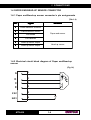
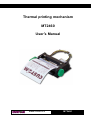
Thermal printing mechanism MT2460 User’s Manual www.custom.it MT2460 All rights reserved. Total or even partial reproduction of this manual in any form, whether on paper or electronically, is strictly forbidden. While CUSTOM ENGINEERING SPA guarantees that the information contained in this manual has been carefully checked and verified, CUSTOM ENGINEERING SPA and other resources utilized in its creation assume no responsibility for situations arising from its use. Feedback regarding any errors in the manual’s content or suggestions on how it could be improved would be greatly appreciated. Since its products are subject to continuous checking and improvement, CUSTOM ENGINEERING SPA reserves the right to modify the information contained in this manual without prior notice. COD. DOME - MT2460 VERS. 1.00 Copyright 2002 CUSTOM ENGINEERING SPA – Italy CUSTOM ENGINEERING SPA Str. Berettine 2 - 43010 Fontevivo (PARMA) - Italy Tel. : +39 0521-680111 Fax : +39 0521-610701 http: www.custom.it To contact our Technical Support : Phone. : +39 0521-680163 Fax : +39 0521-680146 Email : [email protected] MT2460 Printing mechanism models MT2460 A. Front exterior view MT2460 1- Motor 2- Print Head 3- Head up lever 4- Sensor Head up detection 5- Knob paper feed 6- Thermal head connector A- Paper outfeed B- Paper input C- Paper end sensor 5 2 1 A C MT2460 TABLE OF CONTENTS INTRODUCTION CONVENTIONS USED IN THE MANUAL ..................................................... 1 GENERAL SPECIFICATIONS ...................................................................... 2 DESCRIPTION OF THE MECHANISM ......................................................... 3 MAIN FEATURES ........................................................................................... 4 1. CONNECTIONS 1.1 CONNECTIONS TERMINALS ............................................................. 1.2 THERMAL HEAD CONNECTOR ......................................................... 1.2.1 Thermal head connector’s pin assignment ................................ 1.3 MOTOR CONNECTOR ........................................................................ 1.3.1 Motor connector’s pin assignment ............................................. 1.3.2 Electrical circuit block diagram of motor .................................... 1.4 PAPER END/HEAD-UP CONNECTOR ............................................... 1.4.1 Paper end/Head-up sensor connector’s pin assignment .......... 1.4.2 Electrical circuit block diagram of paper end/head-up sensor ... 1-1 1-2 1-2 1-3 1-3 1-3 1-4 1-4 1-4 2. PRINT HEAD 2.1 PRINT HEAD ........................................................................................ 2.2 OPERATION PRECAUTIONS ............................................................. 2.3 BLOCK DIAGRAM OF ELECTRICAL SERIES CIRCUIT .................. 2.3.1 Head division processing ............................................................... 2.4 PRINTING DATA AND PRINTING POSITION .................................... 2.5 ELECTRICAL CHARACTERISTICS OF CIRCUIT ............................ 2.6 SWITCHING CHARACTERISTICS OF CIRCUIT .............................. 2.7 TIMING CHART.................................................................................... 2.8 THERMISTOR ...................................................................................... 2.8.1 Thermistor curve ............................................................................ i MT2460 2-1 2-1 2-2 2-2 2-3 2-4 2-5 2-6 2-6 2-8 TABLE OF CONTENTS 3. STEPPER MOTOR 3.1 STEPPER MOTOR .............................................................................. 3.1.1 Technical specifications ................................................................. 3.1.2 Excitation sequence ....................................................................... 3.2 PRECAUTION ...................................................................................... 3-1 3-1 3-2 3-2 4. SENSOR 4.1 SENSOR............................................................................................... 4-1 4.2 GRAPHICS OF TYPICAL CHARACTERISTICS ................................ 4-2 5. DIMENSIONS 5.1 DIMENSIONS ....................................................................................... 5-1 MT2460 ii INTRODUCTION CONVENTIONS USED IN THE MANUAL N.B. Gives important information or suggestions relative to the use of the printer WARNING The information marked with this symbol must be carefully heeded to safeguard against damaging the printer DANGER The information marked with this symbol must be carefully heeded to safeguard against injury to the operator. 1 MT2460 INTRODUCTION GENERAL SPECIFICATIONS (Tab. 1) Item Specification Printing method Thermal line dot method Effective printing width 56mm ± 0,2mm Head configuration (dots/line) 448 Dot Pitch 0.125 mm horizontal 0.125 mm vertical Printing Speed (see power consumption and energy for dots) 150 mm/s Paper width (mm) 60 ± 0,5 Paper feed method Friction feed, 1 dot line/1 pulses, bipolar 2-2 phase excitation Head temperature sensor Thermistor Paper detection Reflective type photosensor Maximum number of dots activated at a time 192 700 Ω ± 3% Dot resistance (Rav) Number of strobes 3 5°C Header energy 25°C 40°C 0,165mJ/dot (0,22 ms) 0,15mJ/dot (0,20 ms) 0,14mJ/dot (0,19 ms) 23 Ω Driver saturated resistance (Ric) External dimensions (W x D x H) 85,4 x 49 x 20 Weight 72 gr. Operation Voltage range logic 5V ± 10% Operation Voltage dotline head 22,8 ÷ 25,2 V Current consumption 31 mA/dots Life/Reability Recommanded paper MT2460 50 K m Kanzan KF50 or equivalent 2 INTRODUCTION Maximum ratings Parameter (Tab. 2) Specification Head voltage 25,2 V (note between connectors) Logic voltage Vdd = +5V ± 0,25V Environment operating temperature range 0 ÷ 50°C 10 ÷ 90% RH no condensation Operating humidity Storage environmental Maximum operating temperature -40 ÷ 80°C Humidity 10 ÷ 90% no condensation, Paper excluded Detected temperature of thermistor shall not exceed 65°C DESCRIPTION OF THE MECHANISM With the MT2460 mechanim Custom shows a new line of thermal plastic printing mechanisms; the new serie offers the possibility to achieve the high performances together with a very compact layout. The MT2460 mechanisms prints at a high 203 dpi resolution on paper weights between 60 and 120 gr/m2 (also labels). The mechanism is featured with a high torque paper-pulling motor, and with a silicon rubber roll. 3 MT2460 INTRODUCTION MAIN FEATURES • • • • • • • • • • • • Paper width from 60 mm. Autoloading capability. High printing speed up to 65 mm/sec. Logic voltage 24V. Possibility to manage paper thickness from 60 to 120 gr/m2 (also labels). Sensors: Paper end sensor, head up detection, temperature sensor thermistor 30K. Life 50 Km Printed paper. Compact Layout. Double paper inlet : straight and 90°. Possibility to have the kit of integrated autocutter. New generation of printing head with a high performance. Options : Control board, notch sensor. MT2460 4 1. CONNECTIONS Paper control connector (Fig.1.1) 6 1 4 1 1 M otor connector Therm al head connector 15 1.1 CONNECTIONS TERMINALS The MT2460 mechanism has 3 interface connectors (see fig. 1.1), thermal head connector, motor connector and paper control connector. In the table below aredescribed the connector specifications and functions : (Tab.1.1) N o. Connector Pin No. Type 1 Thermal head connector 15 JST connector (or equivalent) Male S15B-PH-K-S 6 Molex connector (or equivalent) female housing 51021-0600 terminal 50058-800 4 Molex connector female housing 51021-0400(white) terminal 50058-8000 Head-up sensor 2 Paper end sensor 3 Motor connector 1-1 MT2460 1. CONNECTIONS 1.2 THERMAL HEAD CONNECTOR 1.2.1 Thermal Head connector’s pin assignments (Tab.1.2) N o. Signal Function 1 VH HEAD POWER SUPPLY 2 VH HEAD POWER SUPPLY 3 VH HEAD POWER SUPPLY 4 GND GROUND 5 GND GROUND 6 GND GROUND 7 VD D LOGIC POWER SUPPLY 8 TM THERMISTOR 9 STB1 STROBE1 SIGNAL 10 10 STB2 STROBE2 SIGNAL 11 11 STB3 STROBE3 SIGNAL 12 12 N.C. NOT CONNECTED 13 13 CLOCK SERIAL CLOCK 14 14 LATCH LATCH 15 15 DATA IN DATA INPUT MT2460 1-2 1. CONNECTIONS 1.3 MOTOR CONNECTOR 1.3.1 Motor connector’s pin assignments (Tab.1.3) N o. Signal Remarks 1 MOTA+ Phase 1 coil 2 MOTB+ Phase 2 coil 3 MOTA- Phase 1 coil 4 MOTB- Phase 2 coil 1.3.2 Electrical circuit block diagram of motor (Fig.1.3) 1 M O TA+ 3 M O TA- 2 M O TB+ M otor 4 M O TB- 1-3 MT2460 1. CONNECTIONS 1.4 PAPER END/HEAD-UP SENSOR CONNECTOR 1.4.1 Paper end/Head-up sensor connector’s pin assignments (Tab.1.4) N o. Signal 1 Photo-transistor collector 2 Photo-transistor emitter Remarks Paper-end sensor 3 Led anode 4 Led cathode 5 Head-up sensor output 6 Head-up sensor output Head-up sensor 1.4.2 Electrical circuit block diagram of Paper end/Head-up sensor (Fig.1.4) A 3 K C 4 1 E 2 SW 1 5 SW 2 6 MT2460 1-4 2. PRINT HEAD 2.1 PRINT HEAD MT2460 has a thickfilm thermal printhead. Scanning Line Time (SLT) is the time to print one complete line using all strobes available. The relation between the printhead supply voltage and “On Time” (Ton) is as follows: (Tab.2.1) 2 VHead x Rav Po = Io2 x Rav = (Rav + Ric)2 Symbol Parameter Unit Rav Average resistance 700 Ω Ric Driver Saturated Resistance 23 Ω Eo Ton = Po 2.2 OPERATION PRECAUTIONS 1. When continuous printing is performed the supply energy should be reduced so that the substrate temperature show in Maximum Condition Table 2. Power On and Off sequence must be in the following order to prevent the dot element damage: Turn On= Apply the logic supply voltage (Vdd) first and then the printhead supply voltage. Turn Off= Switch off the printhead supply voltage first and then turn the logic voltage off. 3. The printhead shall be disabled in STB during Power ON/OFF, or Power (VH)-Logic(Vdd) sequence described in note 2 shall be kept. 4. Heat elements and IC’s shall be anti-electrostatic in order to prevent the electrostatic destruction. Do not touch the connector pins with naked hands. 5. The printhead substrate surface is coated with glass and mechanical stress or shock (including dust scratch damage) should be avoided to prevent damage. 6. When the printhead operation is finished, printsupply voltage (including the charged voltage with capacitor) should be reduced to the ground level and remained until next printhead operation occur. 7. Condensation should be avoided. If condensation occurred, do not switch on the printhead power until condensation disappear. 8. If printing sound, for example sticking sound, occured, please adjust the paper feed speed or pulse to avoid these kind of mechanical resonance. 9. Please pay attention that the paper used does not include bad factor to affect printhead life. 10. The print density variation may become larger if the number of dots energized at same time becomes greater than the 192 value. 2-1 MT2460 2. PRINT HEAD 2.3 BLOCK DIAGRAM OF THE ELECTRICAL CIRCUIT 1, 2, 3 V H (+24V ) 448 321 320 129 128 1 4, 5, 6 GND TM 8 V D D (+ 5V ) 7 S TB 3 11 S TB 2 10 S TB 1 9 LAT C H 14 D ATA IN 15 CLOCK 13 TH ER M IS TO R 30K Ω B :3950 LATC H R E G ISTE R 448 B IT S H IFT R E G ISTE R 15 P IN (Fig.2.1) Notes : Symbol “ “ : means a negative logic signal. 2.3.1 Head Division Processing The thermal head has 3 strobes, and print divide into up 3 times is possible. The relation between strobes and position of heting elements is shown in the following table : (Tab.2.2) S TB N o. D ot N o. Dots/STB 1 1 ~ 128 128 2 129 ~ 256 128 3 257 ~ 448 192 MT2460 2-2 2. PRINT HEAD 2.4 PRINTING DATA AND PRINTING POSITION The data of 448 bits (1 to 448) transferred by DATA IN (DI) are printed in the arrangement as shown in the following figure : (Fig.2.2) P a p er fee d in g d ire ctio n P rin ting p a p er P rin ting side P rin ting d a ta D ATA IN P rin te r m e ch a n ism M oto r 2-3 MT2460 2. PRINT HEAD 2.5 ELECTRICAL CHARACTERISTICS OF CIRCUIT (Tab.2.3) Item SYMBOL MINI TYP. MAXI. Unit Head power supply VH 23.5 24.0 24.5 V Logic power supply V dd 4.75 5.0 5.25 V Logic supply current Idd - - 31.5 mA Input Voltage (High) VIH 0.8xVdd - V dd V Input Voltage (Low) VIL 0 - 0.2xVdd V Data input current (DI) High (1) ILHDI - - 0.5 uA Data input current (DI) Low ILLDI - - -0.5 uA STB 1 to 3 input current (High) (1) IIHSTR - - 1.5 uA STB 1 to 3 input current (Low) IILSTR - - -165 uA Clock input current (High) (1) ILHCLK - - 3.5 uA Clock input current (Low) IILLCLK - - -3.5 uA Latch input current (High) (1) IIHLAT - - 3.5 uA Latch input current (Low) IILLAT - - -3.5 uA Data out output voltage (High) VDOH 4.45 - - V Data out output voltage (Low) VDOL - 1.3 2.0 V fCLK 0.1 1.0 3.5 MHz Clock frequency (1) Note: Each strobe includes pull-up resistance of 300KΩ ± 50%. MT2460 2-4 2. PRINT HEAD 2.6 SWITCHING CHARACTERISTICS OF CIRCUIT The switching characteristic summarized in the following table : Item (Tab.2.4) SYMBOL MINI TYP. MAXI. Unit Clock frequency fMAX - - 4.0 Mhz Clock pulse width tw(T) 70 - - ns Data setup time tsu(D) 50 - - ns Data hold time th(D) 40 - - ns Latch setup time tsu(LA) 100 - - ns Latch pulse width tw(LA) 100 - - ns Strobe setup time tsu(STB) 100 - - ns Strobe to driver Otuput delay time TpLH TpHL - - 3.5 µs (Fig.2.3) tw (T) CL OCK DA TA IN tsu (D) th(D) tw(LA ) LA TC H tsu(LA) tsu(STB) ST RO BE tpLH OU TP UT VO LTAG E 2-5 MT2460 2. PRINT HEAD 2.7 TIMING CHART (Fig.2.4) 1.0 M H z CLO CK DAT A I N LA T C H ST RO BE 1,2 ts ST RO BE 3 0.625 m s 1 line 24V VH Notes : Symbol “ “ : means a negative logic signal. 2.8 THERMISTOR The thermistor is very important to adjust the strobe time (Tstrobe) ~ (SLT) in function of the head temperature and to monitor the temperature to prevent the head damage if the temperature is over the limit described in the Maximum conditions table. • • • • Resistance R25 : B value : Operating temperature : Time costant : 30 KΩ ± 5% at 25°C 3950 K ± 2% –20 ~ + 80°C Max. 30 sec.(in the air) Then the resistance value, R, versus temperature , T (in °C) is given by the formula : R(T) = R25 * e {B*(1/TX – 1/T25)} MT2460 2-6 2. PRINT HEAD (Tab.2.5) Temperature (°C) Thermistor Resistance (R) MIN. (KΩ) TYP. (KΩ) MAX. (KΩ) -20.0 268.8 296.6 326.5 -15.0 202.7 222.3 243.2 -10.0 154.2 168.2 182.9 -5.0 118.4 128.4 138.9 0.0 91.70 98.90 106.4 5.0 71.65 76.71 82.10 10.0 56.20 59.99 63.88 15.0 44.50 47.27 50.10 20.0 35.49 37.53 39.58 25.0 28.50 30.00 31.50 30.0 22.84 24.14 25.46 35.0 18.42 19.55 20.71 40.0 14.95 15.93 16.94 45.0 12.20 13.06 13.94 50.0 10.02 10.76 11.54 55.0 8.271 8.920 9.596 60.0 6.864 7.430 8.021 65.0 5.726 6.219 6.738 70.0 4.799 5.230 5.686 2-7 MT2460 2. PRINT HEAD 2.8.1 Thermistore Curves (Fig.2.5) 350,000 250,000 200,000 150,000 100,000 50,000 Temperature (°C) MT2460 2-8 70,00 65,00 60,00 55,00 50,00 45,00 40,00 35,00 30,00 25,00 20,00 15,00 10,00 5,00 0,00 -5,00 -10,00 -15,00 0,000 -20,00 Resistance (KOhm) 300,000 3. STEPPER MOTOR 3.1 STEPPER MOTOR The paper feed pitch for stepper motor is 2 steps for one dotline(1). (1) Note: 1 dotline = 0.125 mm. 3.1.1 Technical specifications (Tab.3.1) Item Specification Drive voltage D C 24 V N o . o f p h ases 2 Drive mode Bipolar drive Step angle 18° ± 10% Rated current 350 mA / Phase Resistance 12Ω ± 7% at 25 °C (each phase) Inductance 5.7 mH ± 25% at 25°C (1kHz. 1Vrms ) Holding torque 85 gf-cm MIN Pull-out torque 45 gf−cm MIN Insulation resistance 100 MΩ MIN (500 Vdc) Insulation class Class E Dielectric strength 5 mA (at 600V AC 1.0 sec.) Life 210 Hr min. Maximum coil temperature 115°C 3-1 MT2460 3. STEPPER MOTOR 3.1.2 Excitation sequence The motor is driven in the forward direction if its excitation phases are switched as per the following steps : Signal (Tab.3.2) S eq u en ce A+ A+ AA- B+ B+ BB- Step1 High Low Low High Step2 High Low High Low Step3 Low High High Low Step4 Low High Low High Excitation Voltage Waveforms 1dot line (A) H STEP1 STEP2 (Fig.3.1) STEP3 STEP4 L (A) H L (B) H L (B) H L 3.2 PRECAUTION 1. Drive the motor with mosfet driver to obtain the maximum torque force instead transistor driver , transistor driver lose voltage VCEsat *2. 2. Please check the ratio print/pause to prevent the overtemperature on stepper motor. 3. If the motor is driven by more than 24 volts we suggest to use a chopper driving, in order to reduce current, please contact CUSTOM ENGINEERING SPA for further information. MT2460 3-2 4. SENSOR 4.1 SENSOR Maximum Ratings (Tab.4.1) (Ta = 25°C) Parameter Symbol Rating Unit IF 50 mA ∆ IF /°C -0.67 mA/°C Pulse forward current (1) IFP 400 mA Reverse voltage VR 5 V Collector-emitter voltage V C EO 30 V Emitter-collector voltage V EC O 5 V PC 50 mW ∆ P C /°C -0.67 mW/°C IC 20 mA Operating temperature range T opr -25 ~ 85 °C Storage temperature range T stg -30 ~ 100 °C Forward current L E D D E T E C T O R (1) Forward current derating (Ta > 25°C) Collector power dissipation Collector power dissipation derating (Ta > 25°C) Collector current NOTE: Pulse width 100 ≤ µs, Repetitive frequency = 100 Hz. Opto-electrical characteristics Parameter LE D Conditions MIN. TYP. MAX. Unit Forward voltage VF IF = 10mA 1.00 1.15 1.30 V Reverse current IR V R = 5V - - 10 µA Peak emission wavelength λP IF = 10mA - 940 - nm ICEO V CE = 10V, IF = 0 - - 0.1 µA - 900 - nm λP Collector current (2) Leakage current (2) (Tab.4.2) Symbol Collector dark current DETECTOR Peak sensibility wavelength COUPLED (Ta = 25°C) Collector-emitter saturation voltage IC V CE = 5V, IF = 10mA 50 - 750 µA ILEAK V CE = 5V, IF = 10mA - - 0.1 µA IF = 10mA, IC = 25µA - 0.15 0.4 V V CC = 10V, IC = 1 mA R L = 1K Ω - 10 - µs - 10 - µs V CE (sat) Rise time tr Fall time tf NOTE: IC classification R: 50 ~ 150 µΑ, O : 110 ~ 330 µΑ. 4- 1 MT2460 4. SENSOR 4.2 GRAPHICS OF TYPICAL CHARACTERISTICS Forw ard current I F ( m A ) Forward Current vs. Ambient Temperature 50 40 30 20 10 0 0 40 20 60 80 100 120 140 (Fig.4.1) A m bient tem perature Ta (°C ) Collector Power dissipation vs. Ambient Temperature Collector power dissipation Pc ( m W ) 50 40 30 20 10 0 0 20 40 60 80 100 120 Am bient tem perature Ta (°C) MT2460 4- 2 (Fig.4.2) 4. SENSOR Forward Current vs. Forward Voltage 50 Forw ard current I F ( m A ) Ta = 25 °C 30 10 Ta = 75 °C 50 5 25 0 -25 3 1 0 .9 1 .0 1 .1 1 .2 1 .3 1 .4 1 .5 (Fig.4.3) Forw ard voltage V F (V ) Collector Current vs. Forward Current Collector current I C ( µA ) 3 0 00 1 0 00 500 S A M PL E A 300 B C 100 50 Ta = 25 °C 30 V C E = 5V V C E = 0.4V 10 1 3 10 30 100 300 1 0 00 (Fig.4.4) Forw ard current I F ( m A ) 4- 3 MT2460 4. SENSOR Collector Current vs. Collector-Emitter Voltage 60 0 (Fig.4.5) Collector current I C ( µA ) Ta = 25 °C 50 0 20 40 0 16 30 0 12 20 0 8 I F = 4m A 10 0 0 0 2 4 6 8 10 12 14 Collector em itter voltage V CE (V) Collector-Emitter Saturation Voltage vs Ambient temperature 0 .2 4 (Fig.4.6) Collector em itter saturation voltage V C E(S AT ) (V) IF = 1 0 m A I C = 2 5 µA 0 .2 0 0 .1 6 0 .1 2 0 .0 8 0 .0 4 0 - 40 - 20 0 20 40 60 80 Am bient tem perature Ta (°C) MT2460 4- 4 100 4. SENSOR Dark current vs Ambient temperature (Fig.4.7) D ark Current I D (I CE O ) ( µA) 1 10 -1 V C E = 1 0V 10 5 -2 10 10 -3 -4 0 20 40 60 80 1 00 1 20 1 40 Am bient tem perature Ta (°C) 4- 5 MT2460 5. DIMENSIONS 5.1 DIMENSIONS The figure 5.1 illustrates the overall dimensions for the MT2460 thermal printing mechanism. (Fig.5.1) (Dimensions in mm) 2,25 38 50 85,4 5- 1 13,3 49 44,25 58,3 5,65 20 MT2460