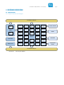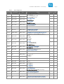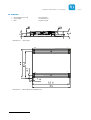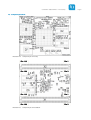
1
TQMa53
User's Manual
TQMa53 UM 200
28.03.2013
User's Manual l TQMa53 UM 200 l © 2013 TQ-Group
Page i
TABLE OF CONTENTS
1.
1.1
1.2
1.3
1.4
1.5
1.6
1.7
1.8
1.9
2.
2.1
3.
3.1
3.1.1
3.1.2
3.2
3.2.1
3.2.1.1
3.2.1.2
3.2.1.3
3.2.1.4
3.2.1.5
3.2.1.6
3.2.2
3.2.2.1
3.2.2.2
3.2.2.3
3.2.3
3.2.4
3.2.5
3.2.6
3.2.7
3.2.8
3.2.9
3.2.10
3.2.11
3.2.11.1
3.2.11.2
3.2.11.3
3.2.11.4
3.2.11.5
3.2.12
3.2.12.1
3.2.12.2
3.2.12.3
3.2.12.4
3.2.12.5
3.2.12.6
3.2.12.7
3.2.12.8
3.2.12.9
3.2.12.10
3.2.13
3.2.14
3.2.14.1
3.2.14.2
3.2.14.3
ABOUT THIS MANUAL................................................................................................................................................................................ 1
Copyright and licence expenses ............................................................................................................................................................ 1
Registered trademarks .............................................................................................................................................................................. 1
Disclaimer ...................................................................................................................................................................................................... 1
Imprint ............................................................................................................................................................................................................ 1
Tips on safety................................................................................................................................................................................................ 2
Symbols and typographic conventions ............................................................................................................................................... 2
Handling and ESD tips ............................................................................................................................................................................... 2
Naming of signals ....................................................................................................................................................................................... 3
Further applicable documents / presumed knowledge ................................................................................................................. 3
BRIEF DESCRIPTION .................................................................................................................................................................................... 4
Key functions and characteristics:.......................................................................................................................................................... 4
ELECTRONICS SPECIFICATION ................................................................................................................................................................. 5
System overview ......................................................................................................................................................................................... 5
System architecture / block diagram .................................................................................................................................................... 5
Functionality ................................................................................................................................................................................................. 6
System components .................................................................................................................................................................................. 7
i.MX53 processor details ........................................................................................................................................................................... 7
i.MX53 processor versions ........................................................................................................................................................................ 7
CPU errata...................................................................................................................................................................................................... 7
Boot mode..................................................................................................................................................................................................... 8
Boot configuration...................................................................................................................................................................................... 8
Boot interfaces ............................................................................................................................................................................................. 9
Pin multiplexing .......................................................................................................................................................................................... 9
Memory ....................................................................................................................................................................................................... 11
DDR3 SDRAM............................................................................................................................................................................................. 11
eMMC NAND flash ................................................................................................................................................................................... 11
EEPROM ....................................................................................................................................................................................................... 12
Temperature sensor ................................................................................................................................................................................ 12
RTC ................................................................................................................................................................................................................ 13
Ethernet....................................................................................................................................................................................................... 14
SD card ........................................................................................................................................................................................................ 14
GPIO ............................................................................................................................................................................................................. 15
JTAG ............................................................................................................................................................................................................. 16
Touch ........................................................................................................................................................................................................... 16
External Memory Bus .............................................................................................................................................................................. 17
Graphics interfaces .................................................................................................................................................................................. 18
CSI ................................................................................................................................................................................................................. 18
DISP1 ............................................................................................................................................................................................................ 18
LCD control ................................................................................................................................................................................................ 18
LVDS ............................................................................................................................................................................................................. 19
VGA ............................................................................................................................................................................................................... 19
Serial interfaces......................................................................................................................................................................................... 20
CAN............................................................................................................................................................................................................... 20
FIRI ................................................................................................................................................................................................................ 20
I2C ................................................................................................................................................................................................................. 20
I2S.................................................................................................................................................................................................................. 21
1-Wire........................................................................................................................................................................................................... 21
SATA ............................................................................................................................................................................................................. 21
SPDIF ............................................................................................................................................................................................................ 21
SPI ................................................................................................................................................................................................................. 22
UART............................................................................................................................................................................................................. 23
USB ............................................................................................................................................................................................................... 24
Reset............................................................................................................................................................................................................. 25
Supply .......................................................................................................................................................................................................... 26
Overview module supply....................................................................................................................................................................... 26
Module / carrier board Power-Up sequence ................................................................................................................................... 27
PMIC signals ............................................................................................................................................................................................... 27
User's Manual l TQMa53 UM 200 l © 2013 TQ-Group
Page ii
TABLE OF CONTENTS (continued)
3.3
3.3.1
3.3.2
3.3.3
4.
4.1
4.2
4.3
4.3.1
4.3.2
4.3.3
4.3.4
4.3.5
5.
6.
6.1
6.2
6.3
6.4
6.5
6.6
6.6.1
6.6.2
6.7
6.8
7.
7.1
7.2
Module interface ...................................................................................................................................................................................... 27
Pin assignment ......................................................................................................................................................................................... 27
Pinout module connector X1 ............................................................................................................................................................... 28
Pinout module connector X2 ............................................................................................................................................................... 29
MECHANICS ............................................................................................................................................................................................... 30
Module connectors ................................................................................................................................................................................. 30
Dimensions ................................................................................................................................................................................................ 31
Component placement .......................................................................................................................................................................... 32
Adaptation to the environment .......................................................................................................................................................... 33
Protection against external effects ..................................................................................................................................................... 33
Thermal management ............................................................................................................................................................................ 33
Structural requirements ......................................................................................................................................................................... 33
Notes of treatment .................................................................................................................................................................................. 33
SOFTWARE.................................................................................................................................................................................................. 33
SAFETY REQUIREMENTS AND PROTECTIVE REGULATIONS ......................................................................................................... 34
EMC............................................................................................................................................................................................................... 34
ESD................................................................................................................................................................................................................ 34
Operational safety and personal security ......................................................................................................................................... 34
Climatic and operational conditions .................................................................................................................................................. 34
Reliability and service life ...................................................................................................................................................................... 35
Environment protection ........................................................................................................................................................................ 35
RoHS compliance ..................................................................................................................................................................................... 35
WEEE regulation ....................................................................................................................................................................................... 35
Batteries ...................................................................................................................................................................................................... 35
Other entries .............................................................................................................................................................................................. 35
APPENDIX ................................................................................................................................................................................................... 36
Acronyms and definitions ..................................................................................................................................................................... 36
References .................................................................................................................................................................................................. 38
User's Manual l TQMa53 UM 200 l © 2013 TQ-Group
Page iii
TABLE DIRECTORY
Table 1:
Table 2:
Table 3:
Table 4:
Table 5:
Table 6:
Table 7:
Table 8:
Table 9:
Table 10:
Table 11:
Table 12:
Table 13:
Table 14:
Table 15:
Table 16:
Table 17:
Table 18:
Table 19:
Table 20:
Table 21:
Table 22:
Table 23:
Table 24:
Table 25:
Table 26:
Table 27:
Table 28:
Table 29:
Table 30:
Table 31:
Table 32:
Table 33:
Table 34:
Table 35:
Table 36:
Table 37:
Table 38:
Table 39:
Table 40:
Table 41:
Table 42:
Table 43:
Table 44:
Table 45:
Table 46:
Table 47:
Table 48:
Terms and Conventions..................................................................................................................................................................... 2
Processor versions ............................................................................................................................................................................... 7
Boot modes i.MX53 ............................................................................................................................................................................. 8
Boot-Mode register BT_FUSE_SEL .................................................................................................................................................. 9
Boot configuration ........................................................................................................................................................................... 10
DDR3 SDRAM ..................................................................................................................................................................................... 11
DDR3-SDRAM address range ........................................................................................................................................................ 11
EEPROM ............................................................................................................................................................................................... 12
Temperature sensor ......................................................................................................................................................................... 12
Current consumption RTC ............................................................................................................................................................. 13
FEC signals .......................................................................................................................................................................................... 14
SD card signals................................................................................................................................................................................... 14
GPIO signals........................................................................................................................................................................................ 15
JTAG modes........................................................................................................................................................................................ 16
JTAG signals........................................................................................................................................................................................ 16
Touch signals ..................................................................................................................................................................................... 16
WEIM signals ...................................................................................................................................................................................... 17
Camera Sensor Interface signals .................................................................................................................................................. 18
Parallel display signals .................................................................................................................................................................... 18
Display control signals .................................................................................................................................................................... 18
LVDS0 signals ..................................................................................................................................................................................... 19
LVDS1 signals ..................................................................................................................................................................................... 19
VGA signals ......................................................................................................................................................................................... 19
CAN1 / CAN2 signals ........................................................................................................................................................................ 20
FIRI signals .......................................................................................................................................................................................... 20
I2C2 signals ......................................................................................................................................................................................... 20
I2C2 address distribution ............................................................................................................................................................... 20
I2S signals............................................................................................................................................................................................ 21
1-Wire signal....................................................................................................................................................................................... 21
SATA signals ....................................................................................................................................................................................... 21
SPDIF signals ...................................................................................................................................................................................... 21
CSPI signals ......................................................................................................................................................................................... 22
ECSPI signals....................................................................................................................................................................................... 22
UART1 signals .................................................................................................................................................................................... 23
UART2 signals .................................................................................................................................................................................... 23
UART3 signals .................................................................................................................................................................................... 23
USB_H1 signals .................................................................................................................................................................................. 24
USB_OTG signals ............................................................................................................................................................................... 24
USB Port Power Control .................................................................................................................................................................. 24
Reset signals ....................................................................................................................................................................................... 25
Parameter module supply ............................................................................................................................................................. 26
PMIC signals ....................................................................................................................................................................................... 27
Pinout module connector X1 ........................................................................................................................................................ 28
Pinout module connector X2 ........................................................................................................................................................ 29
Plug connectors used on the TQMa53 ....................................................................................................................................... 30
Suitable carrier board mating plug connectors ...................................................................................................................... 30
Acronyms ............................................................................................................................................................................................ 36
Further applicable documents ..................................................................................................................................................... 38
User's Manual l TQMa53 UM 200 l © 2013 TQ-Group
Page iv
ILLUSTRATION DIRECTORY
Illustration 1:
Illustration 2:
Illustration 3:
Illustration 4:
Illustration 5:
Illustration 6:
Illustration 7:
Illustration 8:
Illustration 9:
Illustration 10:
Illustration 11:
Illustration 12:
Illustration 13:
Illustration 14:
Illustration 15:
Block diagram TQMa53 (simplified) ....................................................................................................................................... 4
Block diagram TQMa53 .............................................................................................................................................................. 5
Block diagram i.MX537 ............................................................................................................................................................... 7
Block diagram DDR3 SDRAM connection .......................................................................................................................... 11
Block diagram eMMC flash connection .............................................................................................................................. 11
Block diagram EEPROM connection .................................................................................................................................... 12
Block diagram temperature sensor connection .............................................................................................................. 12
Block diagram RTC .................................................................................................................................................................... 13
Block diagram UART2 interface ............................................................................................................................................ 23
Block diagram Reset ................................................................................................................................................................. 25
Block diagram power supply carrier board ....................................................................................................................... 27
Stack height ................................................................................................................................................................................ 31
Overall dimensions (bottom view) ...................................................................................................................................... 31
Component placement top ................................................................................................................................................... 32
Component placement bottom ........................................................................................................................................... 32
User's Manual l TQMa53 UM 200 l © 2013 TQ-Group
REVISION HISTORY
Rev.
Date
Name
100
05.09.2012
Petz
200
28.03.2013
Petz
Pos.
Modification
Document created
All
Complete rework
Page v
User's Manual l TQMa53 UM 200 l © 2013 TQ-Group
Page 1
1. ABOUT THIS MANUAL
1.1 Copyright and licence expenses
Copyright protected © 2013 by TQ-Systems GmbH.
This User's Manual may not be copied, reproduced, translated, changed or distributed, completely or partially in electronic,
machine readable, or in any other form without the written consent of TQ-Systems GmbH.
The drivers and utilities for the used components as well as the BIOS are subject to the copyrights of the respective
manufacturers. The licence conditions of the respective manufacturer are to be adhered to.
Bootloader-licence expenses are paid by TQ-Systems GmbH and are included in the price.
Licence expenses for the operating system and applications are not taken into consideration and must be separately calculated /
declared.
1.2 Registered trademarks
TQ-Systems GmbH aims to adhere to the copyrights of all the graphics and texts used in all publications, and strives to use
original or license-free graphics and texts.
All the brand names and trademarks mentioned in the publication, including those protected by a third party, unless specified
otherwise in writing, are subjected to the specifications of the current copyright laws and the proprietary laws of the present
registered proprietor without any limitation. One should conclude that brand and trademarks are rightly protected by of a third
party.
1.3 Disclaimer
TQ-Systems GmbH does not guarantee that the information in this User's Manual is up-to-date, correct, complete or of good
quality. Nor does TQ-Systems GmbH assume guarantee for further usage of the information. Liability claims against TQ-Systems
GmbH, referring to material or non-material related damages caused, due to usage or non-usage of the information given in the
User's Manual, or due to usage of erroneous or incomplete information, are exempted, as long as there is no proven intentional
or negligent fault of TQ-Systems GmbH.
TQ-Systems GmbH explicitly reserves the rights to change or add to the contents of this User's Manual or parts of it without
special notification.
1.4 Imprint
TQ-Systems GmbH
Gut Delling, Mühlstraße 2
82229 Seefeld
Tel:
+49 (0) 8153 9308–0
Fax:
+49 (0) 8153 9308–134
Email: [email protected]
Web:
http://www.tq-group.com/
User's Manual l TQMa53 UM 200 l © 2013 TQ-Group
Page 2
1.5 Tips on safety
Improper or incorrect handling of the product can substantially reduce its life span.
1.6 Symbols and typographic conventions
Table 1:
Symbol
Terms and Conventions
Meaning
This symbol represents the handling of electrostatic-sensitive modules and / or components. These
components are often damaged / destroyed by the transmission of a voltage higher than about 50 V.
A human body usually only experiences electrostatic discharges above approximately 3,000 V.
This symbol indicates the possible use of voltages higher than 24 V.
Please note the relevant statutory regulations in this regard.
Non-compliance with these regulations can lead to serious damage to your health and also cause
damage / destruction of the component.
This symbol indicates a possible source of danger. Acting against the procedure described can lead to
possible damage to your health and / or cause damage / destruction of the material used.
This symbol represents important details or aspects for working with TQ-products.
Command
A font with fixed-width is used to denote commands, file names, or menu items.
1.7 Handling and ESD tips
General handling of your TQ-products
The TQ-product may only be used and serviced by certified personnel who have taken note of the
information, the safety regulations in this document and all related rules and regulations.
A general rule is: do not touch the TQ-product during operation. This is especially important when
switching on, changing jumper settings or connecting other devices without ensuring beforehand
that the power supply of the system has been switched off.
Violation of this guideline may result in damage / destruction of the module and be dangerous to your
health.
Improper handling of your TQ-product would render the guarantee invalid.
Proper ESD handling
The electronic components of your TQ-product are sensitive to electrostatic discharge (ESD).
Always wear antistatic clothing, use ESD-safe tools, packing materials etc., and operate your TQproduct in an ESD-safe environment. Especially when you switch modules on, change jumper settings,
or connect other devices.
User's Manual l TQMa53 UM 200 l © 2013 TQ-Group
Page 3
1.8 Naming of signals
A hash mark (#) at the end of the signal name indicates a low-active signal.
Example: RESET#
If a signal can switch between two functions and if this is noted in the name of the signal, the low-active function is marked with
a hash mark and shown at the end.
Example: C / D#
If a signal has multiple functions, the individual functions are separated by slashes when they are important for the wiring.
The identification of the individual functions follows the above conventions.
Example: WE2# / OE#
1.9 Further applicable documents / presumed knowledge
•
•
•
•
•
Specifications and manual of the used modules:
These documents describe the service, functionality and special characteristics of the used module (incl. BIOS).
Specifications of the used components:
The manufacturer's specifications of the used components, for example CompactFlash cards, are to be taken note of.
They contain, if applicable, additional information that must be taken note of for safe and reliable operation.
These documents are stored at TQ-Systems GmbH.
Chip errata:
It is the user's responsibility to make sure all errata published by the manufacturer of each component are taken note
of.
The manufacturer’s advice should be followed.
Software behaviour:
No warranty can be given, nor responsibility taken for any unexpected software behaviour due to deficient
components.
General expertise:
Expertise in electrical engineering / computer engineering is required for the installation and the use of the device.
The following documents are required to fully comprehend the following contents:
•
•
•
•
•
Circuit diagram MBa53
CPU Manual IMX53RM
User's Manual STK-MBa53
Documentation of boot loader U-Boot
Documentation of PTXdist
(http://www.denx.de/wiki/U-Boot/Documentation)
(http://www.ptxdist.de)
User's Manual l TQMa53 UM 200 l © 2013 TQ-Group
Page 4
2. BRIEF DESCRIPTION
The User's Manual describes the hardware of the TQMa53, and refers to some software settings. It does not replace the Reference
Manual of the CPU. The TQMa53 is a universal Minimodule based on the Freescale ARM CPU MCIMX53 (i.MX53). The Cortex A8
core of this CPU works with up to 1.2 GHz. The TQMa53 extends the TQC product range and offers an outstanding computing
performance combined with high-performance graphics power.
Illustration 1:
Block diagram TQMa53 (simplified)
The TQMa53 provides the following key functions and characteristics:
2.1 Key functions and characteristics:
•
•
•
•
•
•
•
•
•
•
Freescale CPU i.MX53 (i.MX537 or i.MX535)
Up to 1 Gibyte DDR3 SDRAM
Up to 16 Gibyte eMMC NAND flash
64 Kbit EEPROM
Temperature sensor
Real-time clock
Freescale Power Management Integrated Circuit (PMIC)
All essential CPU pins are routed to the module connectors
Extended temperature range
Single power supply 5 V
User's Manual l TQMa53 UM 200 l © 2013 TQ-Group
Page 5
3. ELECTRONICS SPECIFICATION
SPECIFICATION
3.1 System overview
3.1.1 System architecture / block diagram
Connector 120 pins
I2S
Alt.
USB_H3_ULPI
Alt.
WEIM
Alt.
UART4
Alt.
UART5
ECSPI1
SATA
JTAG
VGA
USB_OTG
Touch
PMIC
DDR3 SDRAM
eMMC
RTC
CSPI
FIRI
I2C3
SPDIF
USB_H1
CSI0
FEC
i.MX537
One-wire
UART3
EEPROM
DC/DC BP
DC/DC 3V2
CAN2
ESDHC2
I2C2
LVDS1
UART2
CAN1
DISP1
(WEIM)
GPIO
(WEIM)
LVDS0
UART1
5V
Connector 120 pins
Illustration 2:
Block diagram TQMa53
Temperature
sensor
User's Manual l TQMa53 UM 200 l © 2013 TQ-Group
3.1.2 Functionality
The following key functions are implemented on the TQMa53:
•
i.MX53 processor
•
DDR3 SDRAM
•
eMMC NAND flash
•
EEPROM
•
Temperature sensor
•
PMIC / DC/DC converter
The following interfaces are provided at the module connectors of the TQMa53:
•
2 × CAN
•
1 × Camera Sensor Interface
•
1 × CSPI (SPI)
•
1 × parallel display (DISP)
•
1 × ESDHC2 (SDIO/MMC/SD card)
•
1 × ECSPI (SPI)
•
1 × Ethernet 10/100 Mbit
•
1 × FIRI (Fast Infrared)
•
2 × I2C
•
1 × I2S
•
2 × LVDS display
•
1 × 1-Wire
•
1 × SATA
•
1 × SPDIF
•
3 × UART (1 × with handshake)
•
2 × USB 2.0 Hi-Speed
•
1 × VGA
•
1 × Touch
•
GPIOs
•
JTAG
•
Boot mode
As an alternative to the factory configuration further interfaces of the i.MX53 can also be used:
•
USB 2.0 Hi-Speed ULPI interface
•
WEIM bus
•
ESDHC1 (SDIO/MMC/SD card)
•
General Purpose Timer
•
PWM
•
More UARTs
Page 6
User's Manual l TQMa53 UM 200 l © 2013 TQ-Group
Page 7
3.2 System components
3.2.1 i.MX53 processor details
The following illustration shows the block diagram of the i.MX53 derivative i.MX537.
Illustration 3:
Block diagram i.MX537
(Source: Freescale)
3.2.1.1 i.MX53 processor versions
Depending on the version of the TQMa53 one of the following versions of the CPU is assembled:
Table 2:
Processor versions
Manufacturer
Part number
Features
800 MHz
Mask Set
N78C
Temperature
–40 to +85 °C
Package
Freescale
MCIMX537CVV8C
19 × 19 mm2 BGA
Freescale
MCIMX535DVV1C
1 GHz
N78C
–20 to +85 °C
19 × 19 mm2 BGA
Freescale
MCIMX535DVV2C
1.2 GHz
N78C
–20 to +85 °C
19 × 19 mm2 BGA
3.2.1.2 CPU errata
Attention: Malfunction
Please take note of the current errata of the Freescale CPU (4).
User's Manual l TQMa53 UM 200 l © 2013 TQ-Group
Page 8
3.2.1.3 Boot mode
The boot mode of the i.MX53 is set with the pins BOOT_MODE0 and BOOT_MODE1.
The following table shows the supported boot modes, as well as the boot mode selected for the TQMa53.
Table 3:
Boot modes i.MX53
BOOT_MODE[1:0]
Boot type
TQMa53
Remark
00
Internal Boot
–
01
Reserved
–
10
Boot From Fuses
X
BOOT_MODE1 10 kΩ PU
BOOT_MODE0 10 kΩ PD
11
Serial Downloader
–
Via USBOTG or UART2
Settings for boot configuration via GPIO pins
–
Both signals BOOT_MODE[1:0] are additionally made available at the module connectors.
All possible boot modes can therefore be set by alternative placement of resistor combinations on the carrier board.
To enable the reading of the boot configuration via the GPIO pins, BOOT_MODE[1:0] has to be set to 00.
For that purpose the pin BOOT_MODE1 has to be pulled low on the carrier board.
The reference voltage for BOOT_MODE[1:0] is VCC2V775, which is also available at the module connectors.
3.2.1.4 Boot configuration
A total of 21 GPIO pins are available for the boot configuration.
Freescale recommends overriding the eFuses by GPIO pins only during development and to burn the necessary eFuses
in the final product.
Note: Boot configuration
The TQMa53 is delivered with no preset boot configuration.
On the TQMa53 none of the 21 boot-configuration pins are connected.
Attention: in the initial state the voltage VDD_FUSE is deactivated on the TQMa53 to prevent eFuses from being burnt
by mistake. Before the eFuses can be burnt the signal VDD_FUSE_EN# on GPIO2_GPIO4 must be pulled low.
The bus signals have to be separated with resistors, because the GPIO pins to read the boot configuration are on these
bus signals. (See Freescale System Development Users Guide (7)).
See also section 3.2.14.2 for notes on the wiring of the configuration resistors.
The following table shows the pins of the boot configuration, or the corresponding eFuses.
To boot from the internal eMMC the recommended settings are blue highlighted in the right column.
The settings for other boot devices are to be taken from the Freescale Reference Manual of the processor (1).
User's Manual l TQMa53 UM 200 l © 2013 TQ-Group
Page 9
3.2.1.5 Boot interfaces
The i.MX53 contains a ROM with integrated boot loader.
After the start the boot code initializes the hardware and then loads the program image from the selected boot device.
The eMMC integrated on the TQMa53 can for example be selected as the standard boot-device. As an alternative to booting
from the integrated eMMC it is also possible to boot from one of the following interfaces:
•
•
•
•
ESDHC2 (e.g. SD card)
ECSPI1 (e.g. serial NOR flash)
SATA
WEIM (e.g. NOR flash)
The boot-device and its configuration, as well as different CPU settings have to be set via different boot mode registers.
Therefore the i.MX53 provides two possibilities:
•
•
To burn internal eFuses and/or
To read dedicated GPIO pins
The exact behaviour during booting depends on the value of the register BT_FUSE_SEL (Default = 0):
•
BT_FUSE_SEL = 0: The values in the eFuses are overwritten by GPIO pins.
•
BT_FUSE_SEL = 1: All boot options are defined exclusively by the values the eFuses.
The following table shows the behaviour of the bit BT_FUSE_SEL in dependence of the chosen boot mode.
(Boot modes see section 3.2.1.3).
Table 4:
Boot-Mode
Boot-Mode register BT_FUSE_SEL
Setting BT_FUSE_SEL
Recommended for
00
0 = Boot mode configuration is taken from GPIOs. (Default)
1 = Boot mode configuration is taken from fuses.
Development
10
0 = Boot using Serial Loader (UART/USB) (Default)
1 = Boot mode configuration is taken from fuses.
Series production
3.2.1.6 Pin multiplexing
Depending on the configuration, the pin multiplexing permits the usage of different pins for different purposes.
This document describes the configuration in the Standard-BSP of TQ-Systems GmbH.
Attention: Destruction or malfunction
Many of the CPU pins permit the usage of several different configurations.
Please heed the notes in the i.MX53 Reference Manual (1) concerning the wiring of these pins
before integration / start-up of your carrier board / Starterkit.
User's Manual l TQMa53 UM 200 l © 2013 TQ-Group
Table 5:
Pin name
Page 10
Boot configuration
Signal TQMa53
eFuse
Setting
0000 = NOR / OneNAND (EIM)
0001 = Reserved
0010 = Hard Disk (PATA / SATA)
0011 = Serial ROM (I2C / SPI)
010x = SD / eSD
011x = MMC / eMMC
eMMC
1xxx = NAND
Fast Boot Support
0 = Normal Boot
1 = Fast Boot
SD/MMC Speed Mode
0 = Normal Speed Mode
1 = High Speed Mode
Default
eMMC
0
0
0
1
0
1
0
0
0
0
0
0
0
0
0
0
0
0
0
1
0
0
0
0
0
1
EIM_A22
DISP1_DAT17
BOOT_CFG1[7]
EIM_A21
DISP1_DAT16
BOOT_CFG1[6]
EIM_A20
DISP1_DAT15
BOOT_CFG1[5]
EIM_A19
DISP1_DAT14
BOOT_CFG1[4]
EIM_A18
DISP1_DAT13
BOOT_CFG1[3]
EIM_A17
DISP1_DAT12
BOOT_CFG1[2]
EIM_A16
DISP1_CLK
BOOT_CFG1[1]
EIM_LBA
GPIO2_GPIO27
BOOT_CFG1[0]
EIM_EB0
DISP1_DAT11
BOOT_CFG2[7]
EIM_EB1
DISP1_DAT10
BOOT_CFG2[6]
EIM_DA0
DISP1_DAT9
BOOT_CFG2[5]
EIM_DA1
DISP1_DAT8
BOOT_CFG2[4]
EIM_DA2
DISP1_DAT7
BOOT_CFG2[3]
EIM_DA3
DISP1_DAT6
BOOT_CFG2[2]
Reserved
0
0
n/a
n/a
BOOT_CFG2[1]
0
0
n/a
n/a
BOOT_CFG2[0]
Security Configuration
00 = Reserved
01 = Open
1x = Closed
1
1
EIM_DA4
DISP1_DAT5
BOOT_CFG3[7]
Reserved
0
0
EIM_DA5
DISP1_DAT4
BOOT_CFG3[6]
Reserved
0
0
EIM_DA6
DISP1_DAT3
BOOT_CFG3[5]
0
1
EIM_DA7
DISP1_DAT2
BOOT_CFG3[4]
0
0
EIM_DA8
DISP1_DAT1
BOOT_CFG3[3]
0
0
EIM_DA9
DISP1_DAT0
BOOT_CFG3[2]
0
0
EIM_DA10
DISP1_DRDY_DE
BOOT_CFG3[1]
Reserved
0
0
n/a
n/a
BOOT_CFG3[0]
Direct External Memory Boot Disable
0 = Direct boot from external memory is allowed
1 = Direct boot from external memory is not allowed
0
0
Reserved
BT_FREQ
0 = ARM Frequency 800
800 MHz
1 = ARM Frequency 400 MHz
BT_MMU_ENABLE
0 = MMU/Cache is disabled by ROM during the boot
1 = MMU/Cache is enabled by ROM during the boot
Bus Width
SD/eSD:
xx0 = 1 Bit
xx1 = 4 Bit
MMC/eMMC:
000 = 1 Bit
001 = 4 Bit
010 = 8 Bit
101 = 4 Bit DDR (MMC 4.4)
110 = 8 Bit DDR (MMC 4.4)
Else – Reserved
AXI / DDR Frequency
Freq uency
0 = 200
200 MHz AXI / 400
400 MHz DDR
1 = 166 MHz AXI / 333 MHz DDR
OSC_FREQ_SEL
0 = 19.2; 24; 26; 27 MHz Auto Detection
1 = OSC Frequency
Frequency 24 MHz
Port Select
00 = ESDHCV2-1
01 = ESDHCV2-2
10 = ESDHCV3ESDHCV3-3
11 = ESDHCV2-4
DLL Override
0 = Boot ROM default
1 = Apply value per fuse field MMC_DLL_DLY[3:0]
Boot Acknowledge Disable
0 = Boot Acknowledge Enabled
1 = Boot Acknowledge Disabled
User's Manual l TQMa53 UM 200 l © 2013 TQ-Group
3.2.2 Memory
3.2.2.1 DDR3 SDRAM
On the TQMa53 DDR3 SDRAM is used. Up to four DDR3 128M16 memory chips are assembled.
Each pair of chips has one common chip select and is together connected to the CPU with a bus width of 32 bit.
The TQMa53 can also be equipped with smaller 64M16 memory chips.
The following block diagram shows how the DDR3 SDRAM is connected to the processor.
Illustration 4:
Block diagram DDR3 SDRAM connection
In the following table the possible variations of the TQMa53 using different types of memory chips are shown:
Table 6:
DDR3 SDRAM
Placement option
Capacity
2 × DDR3 128M16 (2 × TOP assembled)
4 × DDR3 128M16 (2 × TOP and 2 × BOTTOM assembled)
512 Mibyte
1 Gibyte
The SDRAM is mapped to the following address ranges:
Table 7:
DDR3-SDRAM address range
Start address
Size
Chip Select
Remark
0x7000_0000
0xB000_0000
0x2000_0000
0x2000_0000
CS0#
CS1#
DDR3 Top
DDR3 Bottom
3.2.2.2 eMMC NAND flash
An eMMC NAND flash is provided to contain the boot loader and the application software.
In the BSP provided by TQ-Systems GmbH a clock rate of 50 MHz is supported.
The hardware reset of the eMMC is routed via 0 Ω resistors to the signals RESET_IN_MX# and RESET_E-MMC#
(PATA_DATA12 / ball N5). These resistors are, however, not assembled. The use of this function is currently not planned.
The following block diagram shows how the eMMC flash is connected to the processor.
i.MX53
ESDHC3_CLK
ESDHC3_CMD
ESDHC3_DAT[7:0]
Illustration 5:
Block diagram eMMC flash connection
eMMC
CLK
CMD
DAT[7:0]
Page 11
User's Manual l TQMa53 UM 200 l © 2013 TQ-Group
Page 12
3.2.2.3 EEPROM
A serial EEPROM is available for permanent storage of e.g. module characteristics or customers parameters.
The EEPROM is controlled via I2C bus 2 of the processor. The write protection (WP) of the EEPROM is not available.
The following block diagram shows how the EEPROM is connected to the processor.
i.MX53
EEPROM
I2C2_SCL
I2C2_SDA
Illustration 6:
SCL
SDA
Block diagram EEPROM connection
The following table shows the EEPROM used.
Table 8:
EEPROM
Manufacturer
Part number
STM
Capacity
M24C64-WDW6TP
Temperature range
64 kbit
–40 to +85 °C
The I2C address of the EEPROM is 0x50 / 0b1010000.
3.2.3 Temperature sensor
A temperature sensor (LM75A from NXP) for supervision of the module temperature is provided on the TQMa53.
The sensor is placed on the top side of the module (D8 in Illustration 14).
The temperature sensor is connected to the I2C bus 2 of the processor.
The overtemperature detection output of the sensor is not connected to the CPU.
The following block diagram shows how the temperature sensor is connected to the processor.
i.MX53
Temperature sensor
I2C2_SCL
I2C2_SDA
Illustration 7:
SCL
SDA
Block diagram temperature sensor connection
The following table shows the temperature sensor used.
Table 9:
Temperature sensor
Manufacturer
NXP
Part number
LM75ADP
Remark
11 bit ADC
The I2C address of the temperature sensor is 0x48 / 0b1001000.
Error
Max. ±3 °C
Temperature range
–55 to +125 °C
User's Manual l TQMa53 UM 200 l © 2013 TQ-Group
Page 13
3.2.4 RTC
The PMIC used provides an RTC. For the backup supply of the RTC the PMIC provides a pin (LICELL), which is routed to the
module connector. For the RTC to work reliably the voltage at the pin “LICELL” has to be in the range of 2.3 V to 3.6 V.
The i.MX53, as well as the PMIC MC34708 provide an RTC. Additionally the PMIC provides an SRTC support for the i.MX53.
The choice of RTC used depends on the software implementation. More details are to be taken from the Freescale Reference
Manual of the CPU and the PMIC. The accuracy the RTC is mainly determined by the characteristics of the quartz used. The type
FC-135 used on the TQMa53 has a standard frequency tolerance of ±20 ppm at 25 °C.
(Parabolic coefficient: max. –0.04 × 10⁻⁶ / °C2).
The manufacturer of the RTC provides the following values for the typical current consumption:
Table 10:
Current consumption RTC
RTC
Typical current consumption
Remark
PMIC RTC
4.0 µA
Mode RTC / Power Cut
CPU SRTC
<10 µA
–
The PMIC provides the necessary supply voltage and a clock signal for the SRTC of the CPU.
The following block diagram shows the implementation on the TQMa53.
Illustration 8:
Block diagram RTC
The RTC domain of the PMIC on the TQMa53 offers the possibility of a backup supply.
It supports simple coin cells, but also Lithium coin cells or a SuperCap which can also be charged by the PMIC.
Charging methods and electrical characteristics of the pin LICELL are to be taken from the data sheet of the PMIC MC34708 (5).
Is to be taken note of that the typical charging current is only 60 µA.
Concerning the RTC the errata sheet of the PMIC (6) contains two errata (number 5 and 23)
which describe a failure of the RTC or the backup supply which can occur under certain circumstances.
No workaround was provided with regard to these errata on the TQMa53.
To avoid these errata on the target system, the use of an I2C-RTC on the carrier board is recommended.
User's Manual l TQMa53 UM 200 l © 2013 TQ-Group
Page 14
3.2.5 Ethernet
The i.MX53 provides a 10/100 Mbit Fast Ethernet Controller (FEC) with RMII, whose signals are routed to the module connectors.
The following table shows the signals used by the FEC.
Table 11:
FEC signals
Signal name
Direction
Remark
FEC_REF_CLK
I
Ethernet Input Transmit Reference Clock
FEC_TX_EN
O
Ethernet Output Transmit Enable
FEC_TXD[1:0]
O
Ethernet Output Transmit Data
FEC_RX_DV
I
Ethernet Input Receive Data Valid
FEC_RXD[1:0]
I
Ethernet Input Receive Data
FEC_RX_ER
I
Ethernet Input Receive Error
FEC_MDC
O
Ethernet Output Management Data Clock
FEC_MDIO
I/OPU
FEC_RST#
O
Ethernet Output Reset (GPIO)
FEC_INT#
I
Ethernet Input Interrupt (GPIO)
Ethernet Management Data (PU 1.5 kΩ)
3.2.6 SD card
An SD card can be connected to the TQMa53. The Enhanced Secured Digital Host Controller 2 version 2 (ESDHCV2-2) is routed to
the module connectors for this purpose.
The following table shows the signals used by the SD card interface.
Table 12:
Signal name
SD card signals
Direction
Remark
ESDHC2_CLK
O
SD-Card Output Clock
ESDHC2_DAT[3:0]
I/O
SD-Card Data
ESDHC2_CMD
I/O
SD-Card Command
ESDHC2_WP
I
SD-Card Write-Protect
ESDHC2_CD#
I
SD-Card Card-Detect
The supported modes of operation, as well as MMC specifications are to be taken from the Freescale Reference Manual of the
CPU (1).
When required the port ESDHC2 can be configured as a boot device.
User's Manual l TQMa53 UM 200 l © 2013 TQ-Group
3.2.7 GPIO
Besides their interface function most of the pins of the i.MX53 can also be used as GPIOs. All these GPIOs are interruptand therefore wake-up capable. Details are to be taken from the Freescale Reference Manual of the CPU (1).
Moreover several pins marked as GPIO are already available at the module connectors.
The following table shows the signals which can be used as GPIOs.
Table 13:
Signal name
GPIO signals
Direction
Remark
GPIO1_GPIO3
I/O
–
GPIO2_GPIO23
I/O
–
GPIO2_GPIO25
I/O
–
GPIO2_GPIO26
I/O
–
GPIO2_GPIO27
I/O
–
GPIO3_GPIO11
I/O
–
GPIO3_GPIO12
I/O
–
GPIO3_GPIO13
I/O
–
GPIO3_GPIO14
I/O
–
GPIO3_GPIO20
I/O
–
GPIO3_GPIO21
I/O
–
GPIO3_GPIO22
I/O
–
GPIO3_GPIO28
I/O
–
GPIO3_GPIO29
I/O
–
GPIO5_GPIO0
I/O
–
The electrical characteristics of the GPIOs are to be taken from the respective data sheet provided by Freescale (2) / (3).
Page 15
User's Manual l TQMa53 UM 200 l © 2013 TQ-Group
Page 16
3.2.8 JTAG
The i.MX53 provides two JTAG modes, which can be set with the signal at the pin JTAG_MOD.
The following table shows the available modes, as well as the mode set on the TQMa53.
With the assembly option R43 and R45 the mode can be changed.
Table 14:
JTAG_MODE
JTAG modes
Default
Name
Remark
0
X
Daisy Chain All
For common SW debug (high speed and production)
1
–
SJC only
IEEE 1149.1 JTAG compliant mode
The JTAG port works in the power domain 2.775 V. The voltage VCC2V775 is routed to the plug connectors and can be
used as a reference voltage for a JTAG adaptor.
The following table shows the signals used by the JTAG interface.
Table 15:
JTAG signals
Signal name
Direction
Remark
JTAG_TCK
IPD
PD 10 kΩ on TQMa53
JTAG_TMS
IPU
PU 10 kΩ to 2.775 V on TQMa53
JTAG_TDI
IPU
PU 10 kΩ to 2.775 V on TQMa53
JTAG_TDO
O
–
JTAG_TRST#
IPU
PU 10 kΩ to 2.775 V on TQMa53
3.2.9 Touch
The PMIC used on the TQMa53 provides a touch interface which is routed to the module connectors.
A 4-wire touch can be connected here.
The following table shows the signals used by the touch interface.
Table 16:
Signal name
Touch signals
Direction
Remark
TSX1
AI
Left
TSX2
AI
Right
TSY1
AI
Top
TSY2
AI
Bottom
A wake-up by the touch is possible in principle. The practical implementation and the question in which power modes this is
possible depends on the respective software implementation.
User's Manual l TQMa53 UM 200 l © 2013 TQ-Group
Page 17
3.2.10 External Memory Bus
Address and data bus, as well as control signals of the external memory interface of the i.MX53 are available at the module
connectors. The signals of the WEIM bus are mostly on the interfaces DISP1 and ECSPI1. DISP1 and ECSPI1 are not available if the
WEIM bus is used. The chip-selects of the External Memory Bus are configurable. Information is to be taken from the Freescale
Reference Manual of the CPU (1).
The following table shows the signals used, as well as their characteristics on the EMI interface.
Table 17:
WEIM signals
Signal name
Remark
WEIM_DA[15:0]
EMI_NAND_WEIM_DA0
EMI_NAND_WEIM_DA1
EMI_NAND_WEIM_DA2
EMI_NAND_WEIM_DA3
EMI_NAND_WEIM_DA4
EMI_NAND_WEIM_DA5
EMI_NAND_WEIM_DA6
EMI_NAND_WEIM_DA7
EMI_NAND_WEIM_DA8
EMI_NAND_WEIM_DA9
EMI_NAND_WEIM_DA10
EMI_NAND_WEIM_DA11
EMI_NAND_WEIM_DA12
EMI_NAND_WEIM_DA13
EMI_NAND_WEIM_DA14
EMI_NAND_WEIM_DA15
WEIM_D[31:16]
Assigned to: DISP1_DAT9
Assigned to: DISP1_DAT8
Assigned to: DISP1_DAT7
Assigned to: DISP1_DAT6
Assigned to: DISP1_DAT5
Assigned to: DISP1_DAT4
Assigned to: DISP1_DAT3
Assigned to: DISP1_DAT2
Assigned to: DISP1_DAT1
Assigned to: DISP1_DAT0
Assigned to: DISP1_DRDY_DE
Assigned to: GPIO3_GPIO11
Assigned to: GPIO3_GPIO12
Assigned to: GPIO3_GPIO13
Assigned to: GPIO3_GPIO14
Assigned to: VGA_HSYNC
EMI_WEIM_D16
EMI_WEIM_D17
EMI_WEIM_D18
EMI_WEIM_D19
EMI_WEIM_D20
EMI_WEIM_D21
EMI_WEIM_D22
EMI_WEIM_D23
EMI_WEIM_D24
EMI_WEIM_D25
EMI_WEIM_D26
EMI_WEIM_D27
EMI_WEIM_D28
EMI_WEIM_D29
EMI_WEIM_D30
EMI_WEIM_D31
WEIM_CONTROL
Assigned to: ESPI_SCLK
Assigned to: ESPI_MISO
Assigned to: ESPI_MOSI
Assigned to: ESPI_SS1#
Assigned to: GPIO3_GPIO20
Assigned to: GPIO3_GPIO21
Assigned to: GPIO3_GPIO22
Assigned to: LCD_HSYNC
Assigned to: ESPI_SS2#
Assigned to: ESPI_SS3#
Assigned to: DISP1_DAT22
Assigned to: DISP1_DAT23
Assigned to: GPIO3_GPIO28
Assigned to: GPIO3_GPIO29
Assigned to: DISP1_DAT21
Assigned to: DISP1_DAT20
EMI_WEIM_CS0
EMI_WEIM_CS1
EMI_WEIM_OE
EMI_WEIM_RW
EMI_WEIM_EB2
EMI_WEIM_EB3
EMI_WEIM_LBA
EMI_WEIM_WAIT
Assigned to: GPIO2_GPIO23
Assigned to: VGA_VSYNC
Assigned to: GPIO2_GPIO25
Assigned to: GPIO2_GPIO26
Assigned to: ESPI_SS0#
Assigned to: LCD_VSYNC
Assigned to: GPIO2_GPIO27
Assigned to: GPIO5_GPIO0
User's Manual l TQMa53 UM 200 l © 2013 TQ-Group
3.2.11 Graphics interfaces
3.2.11.1 CSI
The i.MX53 has two identical Camera Sensor Interfaces (max. 8192 × 4096 pixel). CSI0 is routed to the module connectors.
The following table shows the signals used, as well as their characteristics of the Camera Sensor Interface (CSI).
Table 18:
Camera Sensor Interface signals
Signal name
Direction
Remark
IPU_CSI0_PIXCLK
I
Camera-Sensor Input Clock
IPU_CSI0_HSYNC
I
Camera-Sensor Input Horizontal Sync
IPU_CSI0_VSYNC
I
Camera-Sensor Input Vertical Sync
IPU_CSI0_[D19:4]
I
Camera-Sensor Input Data
IPU_CSI0_DATA_EN
I
Camera-Sensor Input Data Enable
CCM_CSI0_MCLK
O
Camera-Sensor Output Master Clock
CSI0_PWDN
O
Camera-Sensor Output Power Down (GPIO)
CSI0_RST#
O
Camera-Sensor Output Reset (GPIO)
3.2.11.2 DISP1
The i.MX53 has two parallel Display Interfaces (max. 4096 × 2048 pixel). DISP1 is routed to the module connectors.
Information to different types of displays and supported formats can be taken from the Freescale Reference Manual (1).
The following table shows the signals used by the DISP1.
Table 19:
Parallel display signals
Signal name
Direction
Remark
DISP1_DAT[23:0]
O
Display Output RGB Data
DISP1_HSYNC
O
Display Output Horizontal Sync / i.MX53-Signal: IPU_DI1_PIN2
DISP1_VSYNC
O
Display Output Vertical Sync / i.MX53-Signal: IPU_DI1_PIN3
DISP1_CLK
O
Display Output Clock / i.MX53-Signal: IPU_DI1_DISP_CLK
DISP1_DRDY_DE
O
Display Output Data Enable / i.MX53-Signal: IPU_DI1_PIN15
3.2.11.3 LCD control
The following additional signals are available at the module connectors for control of the displays.
The following table shows the signals used.
Table 20:
Signal name
LCD_POWER_EN
Display control signals
Direction
O
Remark
LCD Power Enable Output (GPIO)
LCD_RESET
O
LCD Reset Output (GPIO)
LCD_BLT_EN
O
LCD Backlight Enable (GPIO)
LCD_CONTRAST
O
LCD Contrast Output (PWM)
Page 18
User's Manual l TQMa53 UM 200 l © 2013 TQ-Group
3.2.11.4 LVDS
The i.MX53 has two integrated LVDS display bridges, which are routed to the module connectors.
The following table shows the signals used by the LVDS0 interface.
Table 21:
Signal name
LVDS0 signals
Direction
LVDS0_CLK_P
Remark
O
–
LVDS0_CLK_N
O
–
LVDS0_TX[3:0]_P
O
–
LVDS0_TX[3:0]_N
O
–
The following table shows the signals used by the LVDS1 interface.
Table 22:
Signal name
LVDS1 signals
Direction
Remark
LVDS1_CLK_P
O
–
LVDS1_CLK_N
O
–
LVDS1_TX[3:0]_P
O
–
LVDS1_TX[3:0]_N
O
–
3.2.11.5 VGA
The i.MX53 has a VGA port, which is routed to the module connectors.
The following table shows the signals used by the VGA interface.
Table 23:
Signal name
VGA signals
Direction
Remark
TVDAC_IOR
AO
–
TVDAC_IOG
AO
–
TVDAC_IOB
AO
–
VGA_HSYNC
O
i.MX53 signal: IPU_DI1_PIN4
VGA_VSYNC
O
i.MX53 signal: IPU_DI1_PIN6
Page 19
User's Manual l TQMa53 UM 200 l © 2013 TQ-Group
Page 20
3.2.12 Serial interfaces
The supported standards, transmission modes and rates of the following interfaces are to be taken from the Freescale Reference
Manual (1).
3.2.12.1 CAN
The i.MX537 provides two integrated CAN controller. The signals of both CAN controllers are made available at the module
connectors. The drivers have to be integrated on the carrier board. The i.MX535 does not provide CAN. For this reason the CAN
functionality is not available in the pin multiplexing.
The following table shows the signals used, as well as their characteristics.
Table 24:
CAN1 / CAN2 signals
Signal name
Direction
CAN1_RXCAN
CAN1_TXCAN
CAN2_RXCAN
CAN2_TXCAN
Remark
I
O
I
O
–
–
–
–
3.2.12.2 FIRI
The i.MX53 provides a Fast Infrared Interface which is routed to the module connectors.
The following table shows the signals used, as well as their characteristics of the Fast Infrared Interface (FIRI).
Table 25:
FIRI signals
Signal name
Direction
FIRI_RXD
FIRI_TXD
Remark
I
O
–
–
3.2.12.3 I2C
The i.MX53 provides three I2C interfaces. The I2C interfaces I2C2 and I2C3 are available at the module connectors.
The following table shows the signals used, as well as their characteristics.
Table 26:
I2C2 signals
Signal name
Direction
I2C2_SCL
I2C2_SDA
I2C3_SCL
I2C3_SDA
I/OPU
I/OPU
I/O
I/O
Remark
4.7 kΩ PU to 3.2 V on TQMa53
4.7 kΩ PU to 3.2 V on TQMa53
–
–
The I2C2 bus is also used for components on the TQMa53. The following devices are connected to the I2C2 bus on the TQMa53:
Table 27:
I2C2 address distribution
Component
Chosen address
EEPROM (M24C64)
Temperature sensor (LM75A)
PMIC (MC34708VM)
0x50 / 0b1010000
0x48 / 0b1001000
0x08 / 0b0001000
In case more devices are connected to the I2C2 bus on the carrier board, the maximum capacitive bus load accordingly to the I2C
standard has to be adhered to. If required additional pull-ups should be provided on the carrier board at the bus.
User's Manual l TQMa53 UM 200 l © 2013 TQ-Group
Page 21
3.2.12.4 I2S
Signals of the digital audio multiplexer 5 via SSI are available at the module connectors to connect an audio-codec via I2S.
The following table shows the signals used by the I2S interface.
Table 28:
Signal name
I2S signals
Direction
Remark
I2S_DIN
I
AUDMUX signal: AUD5_RXD
I2S_DOUT
O
AUDMUX signal: AUD5_TXD
I2S_LRCLK
O
AUDMUX signal: AUD5_TXFS
I2S_SCLK
O
AUDMUX signal: AUD5_TXC
I2S_MCLK
O
CCM signal: SSI_EXT1_CLK
Besides I2S the SSI interface also supports further synchronous modes. Details can be taken from the Freescale Reference Manual
of the CPU (1). Asynchronous SSI modes are not supported in the standard pin-multiplexing.
3.2.12.5 1-Wire
The i.MX53 provides a 1-Wire interface which is routed to the module connectors.
The following table shows the signal used by the 1-Wire interface.
Table 29:
Signal name
1-Wire signal
Direction
OWIRE_LINE
Remark
I/O
–
3.2.12.6 SATA
The i.MX53 provides a SATA controller with integrated PHY.
The following table shows the signals used by the SATA interface.
Table 30:
Signal name
SATA signals
Direction
Remark
SATA_RXP
I
–
SATA_RXM
I
–
SATA_TXP
O
–
SATA_TXM
O
–
When required, the SATA interface can be configured as a boot device.
3.2.12.7 SPDIF
The i.MX53 provides an SPDIF interface with transmit and receive-functionality.
The following table shows the signals used by the SPDIF interface.
Table 31:
Signal name
SPDIF signals
Direction
Remark
SPDIF_IN
I
–
SPDIF_OUT
O
–
User's Manual l TQMa53 UM 200 l © 2013 TQ-Group
Page 22
3.2.12.8 SPI
The i.MX53 provides a CSPI (Configurable Serial Peripheral Interface) and two ECSPIs (Enhanced Configurable SPI).
Primarily CSPI and ECSPI1 are thereof available at the module connectors.
Via multiplexing the signals of the ECSPI2 are also available on other signals.
The signals of the CSPI module provided by the processor are made available as SPI interface 1 at the module connectors.
Furthermore the three Slave Selects SS[2:0]# are available at the module connectors.
The following table shows the signals used by CSPI interface.
Table 32:
Signal name
CSPI signals
Direction
Remark
SPI_SCLK
O
Signal i.MX53: CSPI_SCLK
SPI_MOSI
O
Signal i.MX53: CSPI_MOSI
SPI_MISO
I
Signal i.MX53: CSPI_MISO
SPI_SS[2:0]#
O
Signal i.MX53: CSPI_SS[2:0]#
The signals of the ECSPI1 module provided by the processor are made available as SPI interface 2 at the module connectors.
The signals of the ECSPI1 interface are multiplexed with those of the WEIM bus. ECSPI1 is not available if the WEIM bus is used.
Alternatively five signals can be used to connect a serial display to the display interface 1.
The following table shows the signals used by the ECSPI interface.
Table 33:
Signal name
ECSPI signals
Direction
Remark
ESPI_SCLK
O
Signal i.MX53: ECSPI1_SCLK
ESPI_MOSI
O
Signal i.MX53: ECSPI1_MOSI
ESPI_MISO
I
Signal i.MX53: ECSPI1_MISO
ESPI_SS[3:0]#
O
Signal i.MX53: ECSPI1_SS[3:0]#
When required the port ECSPI1 can be configured as a boot device.
Therefore the signal SS1# has to be used as slave select.
User's Manual l TQMa53 UM 200 l © 2013 TQ-Group
3.2.12.9 UART
The i.MX53 provides five UART interfaces.
UART1, UART2 and UART3 are available at the module connectors.
Illustration 9:
Block diagram UART2 interface
The following table shows the signals used by the UART1 interface.
Table 34:
Signal name
UART1 signals
Direction
Remark
UART1_RXD
I
–
UART1_TXD
O
–
UART2 also provides handshake signals.
It is to be taken note of that in DTE as well as in DCE mode RTS# is always an input and CTS# is always an output.
(See Freescale Reference Manual of the CPU (1).)
The UART2 interface with handshake signals provided by the processor is made available at the module connectors.
The following table shows the signals used by the UART2 interface.
Table 35:
Signal name
UART2 signals
Direction
Remark
UART2_RXD
I
–
UART2_TXD
O
–
UART2_RTS#
I
–
UART2_CTS#
O
–
The following table shows the signals used by the UART3 interface.
Table 36:
Signal name
UART3 signals
Direction
Remark
UART3_RXD
I
–
UART3_TXD
O
–
UART4 and UART5 are available if the I2S interface is not used.
Page 23
User's Manual l TQMa53 UM 200 l © 2013 TQ-Group
Page 24
3.2.12.10 USB
The i.MX53 CPU provides three USB Host Cores and one USB OTG Core.
The Host1-Core and the OTG-Core have an integrated High-Speed-PHY and are available at the module connectors.
The following table shows the signals used by the USB_H1 interface.
Table 37:
Signal name
USB_H1 signals
Direction
Remark
USB_H1_DP
I/O
–
USB_H1_DN
I/O
–
USB_H1_VBUS
AI
Series resistor 100 Ω and capacitor 1 µF to GND on the TQMa53
The following table shows the signals used by the USB_OTG interface.
Table 38:
Signal name
USB_OTG signals
Direction
Remark
USB_OTG_DP
I/O
–
USB_OTG_DN
I/O
–
USB_OTG_VBUS
AI
USB_OTG_ID
Series resistor 100 Ω and capacitor 1 µF to GND on the TQMa53
I
–
A third USB High-Speed interface can be implemented with a ULPI PHY provided by the carrier board.
The USB HOST3 ULPI signals are multiplexed with signals of the Camera Sensor Interface 0 (CSI0).
These are only available if CSI0 is not used.
The TQ-BSP does not support Port Power Control.
If Port Power Control should be used, the signals can be provided by pin multiplexing.
The following table shows the possible pin multiplexing.
Table 39:
Signal
USBOTG_OC
USBOTG_PWR
USBH1_OC
UBH1_PWR
USB Port Power Control
Connector
Signal name
i.MX53 ball
X2-39
CAN2_TX
E5
X1-34
GPIO3_GPIO21
V3
X2-41
CAN2_RX
E6
X1-33
GPIO3_GPIO21
W2
X2-61
GPIO1_GPIO3
A6
X1-73
DISP1_DAT21
W4
X2-49
I2S_MCLK
C8
X1-86
DISP1_DAT20
W5
User's Manual l TQMa53 UM 200 l © 2013 TQ-Group
3.2.13 Reset
The following reset inputs or outputs are available at the module connectors of the TQMa53.
The following block diagram shows the wiring of the reset signals.
Illustration 10:
Block diagram Reset
The following table describes the reset signals which are available at the module connectors.
Table 40:
Signal name
Reset signals
Direction
RESET_IN#
IPU
RESET_OUT#
OOD
GLBRST#
IIPU
Remark
•
•
•
•
Reset input of the i.MX53 System Reset Controller
Generates WARM-Reset of the CPU
On the module: PU 28 kΩ to 2.775 V
Low-active signal
• Reset output of the PMIC
• Can be used for reset inputs of external periphery
• Open Drain, requires pull-up on the carrier board (max. 3.3 V)
•
•
•
•
Global reset input of the PMIC
Generates cold start of the PMIC
Internal pull-up to 1.5 V
To activate GLBRST apply low level for preset time according to PMIC register
GLBRSTTMR[1:0] (see Data sheet PMIC (5))
Page 25
User's Manual l TQMa53 UM 200 l © 2013 TQ-Group
Page 26
3.2.14 Supply
3.2.14.1 Overview module supply
The following table shows some technical parameters of the module supply.
The given current consumption has to be seen as an approximate value.
To estimate the power consumption of the system the Freescale Application Note AN4270 should be heeded as the current
consumption of the TQMa53 strongly depends on the application, the mode of operation and the operating system.
The input voltage of the TQMa53 is 5 V (–10 % to +5 %). This results in an input voltage range of 4.5 V to 5.25 V.
Table 41:
Parameter module supply
Parameter
Value typ.
Remark
Supply voltage VIN
5V
–10 % to +5 %
Current consumption Linux (idle)
420 mA
CPU 800 MHz / BSP without power management
Current consumption Linux (100 %)
580 mA
CPU 800 MHz / BSP without power management
In principle, the CPU supports besides the Dynamic Voltage Scaling the following Power Modes:
•
•
•
RUN
WAIT
STOP
The implementation of the modes depends on the BSP and is not considered here.
All requirements according to hardware are created by using an intelligent PMIC.
The PMIC itself also has different power modes whose implementation depends on the software.
The voltages generated by the PMIC and the DC/DC converters on the TQMa53 are not monitored.
On the TQMa53 the following mechanisms or possibilities to monitor the voltage exist:
•
•
•
•
•
VCC3V8_BP: PMIC function ”BP lower than VBAT_TKRL” switch to Off mode, if BP <3.0 V
(for more information see Data sheet PMIC (5)).
VCC3V8_BP: PMIC ADC channel 2 monitoring of undervoltage or overvoltage in software
(for more information see Data sheet PMIC (5)).
VCC1V1_SW1 (VDDGP): CPU function “Brown-Out-Detection” Power_Fail, if VDDGP <0.8 V
(for more information see Reference Manual CPU (1)).
VCC2V775: Voltage is routed to module connector and can be monitored on the carrier board.
VCC3V2: Optional monitoring on the carrier board can be done with an unused I2C3 pin.
Therefore the pin has to be configured accordingly and a pull-up resistor has to be assembled on the TQMa53.
User's Manual l TQMa53 UM 200 l © 2013 TQ-Group
Page 27
3.2.14.2 Module / carrier board Power-Up sequence
The chronological behaviour of the voltages generated on the carrier board are required for its design because the TQMa53
requires a supply voltage of 5 V, and the 3.2 V I/O voltage of the CPU signals is generated on the TQMa53.
One of following two possibilities must be implemented on the carrier board:
1. The supply voltage of 5 V for the TQMa53 and the carrier board supply of 3.3 V are applied at the same time
2. The 5 V supply voltage for the TQMa53 is present and the carrier board supply of 3.3 V is activated via module pin
VCC2V775. After activation the voltage must be stable within 12 ms.
The following illustration shows the control of a voltage regulator on a carrier board using VCC2V775.
Carrier board
DCDC 3V3 12 ms
VIN
5V
Plug connector
DC IN
3.3 V
ENA
TQMa53
VCC5V
Illustration 11:
VOUT
VCC2V775
Block diagram power supply carrier board
With the procedure described above it is certified that the pull-ups on the carrier board are already supplied with voltage when
the boot-configuration pins are read.
In case the LCD bus signals or the matching multiplexed signals representing the boot configurations pins, are not
used, the reference voltage VCC2V775 available at the module connector can also be used as a pull-up voltage for the
configuration resistors.
Attention: Power-Up sequence
No I/O pins of external components may be driven during the boot-process to avoid crosssupply and errors in the power-up sequence.
3.2.14.3 PMIC signals
The CPU communicates with the PMIC via I2C (I2C2).
The I2C address of the PMIC is 0x08 / 0b0001000.
The following table shows the signals used by the PMIC, which are made available at the module connectors, as well as the
signals, which serve for the communication with the CPU.
Table 42:
PMIC signals
Signal name
PWRON
SYSTEM_DOWN#
PMIC_INT
WDOG#
PMIC_STBY_REQ
PMIC_ON_REQ
Description
− Power on/off button connection 1 to PMIC
− Switch to GND
− Internal pull-up to 1.5 V
Indication of imminent system shutdown to processor
Interrupt to processor
Watchdog output to PMIC
Standby output signal to PMIC
Power on/off connection 2 to PMIC
3.3 Module interface
3.3.1 Pin assignment
When using the processor signals the multiple pin configurations by different processor-internal function units must be taken
note of. The pins assignment listed in sections 3.3.2 and 3.3.3 refer to the corresponding standard BSP of TQ-Systems GmbH.
The electrical and pin characteristics are to be taken from the data sheets of CPU (2), (3) and PMIC (5).
User's Manual l TQMa53 UM 200 l © 2013 TQ-Group
Page 28
3.3.2 Pinout module connector X1
Table 43:
Pinout module connector X1
Ball
I/O
Level
Group
Signal
–
P02
P04
–
R01
R06
T01
R05
T03
U01
T04
U03
P05
P06
–
AA01
W02
AB04
V08
AC06
AB09
U05
V01
Y02
–
AB07
AA08
Y09
AB06
AA07
Y08
AC03
AB03
Y06
AA03
Y05
W04
V04
–
AA09
Y07
AC19
AB20
AC21
–
AC16
AB16
–
AA17
Y17
–
AC17
AB17
–
AA16
Y16
–
AC15
AB15
–
P
I
I
P
I
I
I
I
I
I
I
I
I
I
P
IO
IO
IO
IO
IO
IO
I
O
O
P
O
O
O
O
O
O
O
O
O
O
O
O
O
P
O
O
AO
AO
AO
P
O
O
P
O
O
P
O
O
P
O
O
P
O
O
P
0V
3.3 V
3.3 V
0V
3.3 V
3.3 V
3.3 V
3.3 V
3.3 V
3.3 V
3.3 V
3.3 V
3.3 V
3.3 V
0V
3.3 V
3.3 V
3.3 V
3.3 V
3.3 V
3.3 V
3.3 V
3.3 V
3.3 V
0V
3.3 V
3.3 V
3.3 V
3.3 V
3.3 V
3.3 V
3.3 V
3.3 V
3.3 V
3.3 V
3.3 V
3.3 V
3.3 V
0V
3.3 V
3.3 V
0.7 V
0.7 V
0.7 V
0V
1.2 V
1.2 V
0V
1.2 V
1.2 V
0V
1.2 V
1.2 V
0V
1.2 V
1.2 V
0V
1.2 V
1.2 V
0V
POWER
CSI0
CSI0
POWER
CSI0
CSI0
CSI0
CSI0
CSI0
CSI0
CSI0
CSI0
CSI0
CSI0
POWER
GPIO
GPIO
GPIO
GPIO
GPIO
GPIO
ESPI
ESPI
ESPI
POWER
DISP1
DISP1
DISP1
DISP1
DISP1
DISP1
DISP1
DISP1
DISP1
DISP1
DISP1
DISP1
DISP1
POWER
VGA
VGA
VGA
VGA
VGA
POWER
LVDS0
LVDS0
POWER
LVDS0
LVDS0
POWER
LVDS0
LVDS0
POWER
LVDS0
LVDS0
POWER
LVDS0
LVDS0
POWER
DGND
CSI0_HSYNC
CSI0_VSYNC
DGND
CSI0_D4
CSI0_D6
CSI0_D8
CSI0_D10
CSI0_D12
CSI0_D14
CSI0_D16
CSI0_D18
CSI0_PWDN
CSI0_RST#
DGND
GPIO3_GPIO28
GPIO3_GPIO22
GPIO2_GPIO26
GPIO2_GPIO25
GPIO3_GPIO11
GPIO5_GPIO0
ESPI_MISO
ESPI_MOSI
ESPI_SS2#
DGND
DISP1_DRDY_DE
DISP1_DAT1
DISP1_DAT3
DISP1_DAT5
DISP1_DAT7
DISP1_DAT9
DISP1_DAT11
DISP1_DAT13
DISP1_DAT15
DISP1_DAT17
DISP1_DAT19
DISP1_DAT21
DISP1_DAT23
DGND
VGA_HSYNC
VGA_VSYNC
TVDAC_IOB
TVDAC_IOG
TVDAC_IOR
DGND
LVDS0_CLK_P
LVDS0_CLK_N
DGND
LVDS0_TX0_P
LVDS0_TX0_N
DGND
LVDS0_TX1_P
LVDS0_TX1_N
DGND
LVDS0_TX2_P
LVDS0_TX2_N
DGND
LVDS0_TX3_P
LVDS0_TX3_N
DGND
Pin
1
3
5
7
9
11
13
15
17
19
21
23
25
27
29
31
33
35
37
39
41
43
45
47
49
51
53
55
57
59
61
63
65
67
69
71
73
75
77
79
81
83
85
87
89
91
93
95
97
99
101
103
105
107
109
111
113
115
117
119
2
4
6
8
10
12
14
16
18
20
22
24
26
28
30
32
34
36
38
40
42
44
46
48
50
52
54
56
58
60
62
64
66
68
70
72
74
76
78
80
82
84
86
88
90
92
94
96
98
100
102
104
106
108
110
112
114
116
118
120
Signal
Group
Level
I/O
Ball
DGND
CSI0_PIXCLK
DGND
CSI0_DATA_EN
CSI0_D5
CSI0_D7
CSI0_D9
CSI0_D11
CSI0_D13
CSI0_D15
CSI0_D17
CSI0_D19
CSI0_MCLK
DGND
GPIO3_GPIO20
GPIO3_GPIO29
GPIO3_GPIO21
GPIO2_GPIO27
GPIO2_GPIO23
GPIO3_GPIO13
GPIO3_GPIO14
GPIO3_GPIO12
ESPI_SS1#
ESPI_SS0#
ESPI_SS3#
DGND
ESPI_SCLK
DISP1_CLK
DGND
DISP1_HSYNC
DISP1_VSYNC
DGND
DISP1_DAT0
DISP1_DAT2
DISP1_DAT4
DISP1_DAT6
DISP1_DAT8
DISP1_DAT10
DISP1_DAT12
DISP1_DAT14
DISP1_DAT16
DISP1_DAT18
DISP1_DAT20
DISP1_DAT22
DGND
LVDS1_CLK_P
LVDS1_CLK_N
DGND
LVDS1_TX0_P
LVDS1_TX0_N
DGND
LVDS1_TX1_P
LVDS1_TX1_N
DGND
LVDS1_TX2_P
LVDS1_TX2_N
DGND
LVDS1_TX3_P
LVDS1_TX3_N
DGND
POWER
CSI0
POWER
CSI0
CSI0
CSI0
CSI0
CSI0
CSI0
CSI0
CSI0
CSI0
CSI0
POWER
GPIO
GPIO
GPIO
GPIO
GPIO
GPIO
GPIO
GPIO
ECSPI1
ECSPI1
ECSPI1
POWER
ECSPI1
DISP1
POWER
DISP1
DISP1
POWER
DISP1
DISP1
DISP1
DISP1
DISP1
DISP1
DISP1
DISP1
DISP1
DISP1
DISP1
DISP1
POWER
LVDS1
LVDS1
POWER
LVDS1
LVDS1
POWER
LVDS1
LVDS1
POWER
LVDS1
LVDS1
POWER
LVDS1
LVDS1
POWER
0V
3.3 V
0V
3.3 V
3.3 V
3.3 V
3.3 V
3.3 V
3.3 V
3.3 V
3.3 V
3.3 V
3.3 V
0V
3.3 V
3.3 V
3.3 V
3.3 V
3.3 V
3.3 V
3.3 V
3.3 V
3.3 V
3.3 V
3.3 V
0V
3.3 V
3.3 V
0V
3.3 V
3.3 V
0V
3.3 V
3.3 V
3.3 V
3.3 V
3.3 V
3.3 V
3.3 V
3.3 V
3.3 V
3.3 V
3.3 V
3.3 V
0V
1.2 V
1.2 V
0V
1.2 V
1.2 V
0V
1.2 V
1.2 V
0V
1.2 V
1.2 V
0V
1.2 V
1.2 V
0V
P
I
P
I
I
I
I
I
I
I
I
I
I
P
IO
IO
IO
IO
IO
IO
IO
IO
O
O
O
P
O
O
P
O
O
P
O
O
O
O
O
O
O
O
O
O
O
O
P
O
O
P
O
O
P
O
O
P
O
O
P
O
O
P
–
P01
–
P03
R02
R03
R04
T02
T06
U02
T05
U04
V14
–
W01
AA02
V03
AA06
W08
AC07
Y10
V10
V02
Y03
W03
–
U06
AA05
–
Y01
Y04
–
W10
AC05
V09
W09
AC04
AB05
V07
W07
AA04
V06
W05
V05
–
Y13
AA13
–
AB14
AC14
–
AB13
AC13
–
AB12
AC12
–
Y12
AA12
–
User's Manual l TQMa53 UM 200 l © 2013 TQ-Group
Page 29
3.3.3 Pinout module connector X2
Table 44:
Pinout module connector X2
Ball
I/O
Level
Group
Signal
–
–
–
–
–
–
K04**
L05**
–
A11**
G08**
L03
B07
–
J01
K04
K03
K05
–
E05
E06
D06
E07
–
C08
–
B05
D04
F06
–
A06
A07
A08
E09
–
A10
B10
–
M05
C10
F10
D10
E10
F12
–
C07
D08
C15
E14
–
A19
B19
–
C16
E15
–
C17
A20
E16
–
P
P
P
P
P
P
AI
AI
P
P
IIPU
O
O
P
O
I
I
O
P
O
I
I
O
P
O
P
O
IOPU
IOPU
P
I/O
O
IPU
IPU
P
O
O
P
I
O
O
O
O
I
P
I
I
IO
O
P
IO
IO
P
I
AI
P
O
I
O
P
5V
5V
5V
0V
0V
0V
2.4 V
2.4 V
0V
3.3 V
1.5 V
3.3 V
3.3 V
0V
3.3 V
3.3 V
3.3 V
3.3 V
0V
3.3 V
3.3 V
3.3 V
3.3 V
0V
3.3 V
0V
3.3 V
3.3 V
3.3 V
0V
3.3 V
2.775 V
2.775 V
2.775 V
0V
[1]
[1]
0V
3.3 V
3.3 V
3.3 V
3.3 V
3.3 V
3.3 V
0V
3.3 V
3.3 V
3.3 V
3.3 V
0V
[2]
[2]
0V
3.3 V
5.0 V
2.775 V
3.3 V
3.3 V
3.3 V
0V
POWER
POWER
POWER
POWER
POWER
POWER
TOUCH
TOUCH
POWER
PMIC
PMIC
LCD
LCD
POWER
UART2
UART2
UART2
UART2
POWER
CAN2
CAN2
I2S
I2S
POWER
I2S
POWER
FIRI
I2C2
I2C2
POWER
GPIO
JTAG
JTAG
JTAG
POWER
SATA
SATA
POWER
FEC
FEC
FEC
FEC
FEC
FEC
POWER
SD
SD
SD
SD
POWER
USBOTG
USBOTG
POWER
USBOTG
USBOTG
POWER
SPI
SPI
SPI
POWER
VCC5V
VCC5V
VCC5V
DGND
DGND
DGND
TSX1
TSX2
DGND
LICELL
PWRON
LCD_BLT_EN
LCD_CONTRAST
DGND
UART2_TXD
UART2_RXD
UART2_RTS#
UART2_CTS#
DGND
CAN2_TX
CAN2_RX
I2S_DIN
I2S_LRCLK
DGND
I2S_MCLK
DGND
FIRI_TXD
I2C2_SDA
I2C2_SCL
DGND
GPIO1_GPIO3
JTAG_TDO
JTAG_TMS
JTAG_TRST#
DGND
SATA_TXP
SATA_TXM
DGND
FEC_INT#
FEC_TX_EN
FEC_TXD0
FEC_TXD1
FEC_MDC
FEC_RX_ER
DGND
SD_WP
SD_CD#
SD_CMD
SD_CLK
DGND
USB_OTG_DN
USB_OTG_DP
DGND
USB_OTG_ID
USB_OTG_VBUS
VCC2V775
SPI_SS0#
SPI_MISO
SPI_SCLK
DGND
* PMIC ball.
1
See Serial ATA Specification 2.6.
2
See USB 2.0 Specification.
Pin
1
3
5
7
9
11
13
15
17
19
21
23
25
27
29
31
33
35
37
39
41
43
45
47
49
51
53
55
57
59
61
63
65
67
69
71
73
75
77
79
81
83
85
87
89
91
93
95
97
99
101
103
105
107
109
111
113
115
117
119
2
4
6
8
10
12
14
16
18
20
22
24
26
28
30
32
34
36
38
40
42
44
46
48
50
52
54
56
58
60
62
64
66
68
70
72
74
76
78
80
82
84
86
88
90
92
94
96
98
100
102
104
106
108
110
112
114
116
118
120
Signal
Group
Level
I/O
Ball
VCC5V
VCC5V
VCC5V
DGND
DGND
DGND
TSY1
TSY2
DGND
GLBRST#
RESET_OUT#
LCD_PWR_EN
LCD_RESET
DGND
UART1_RXD
UART1_TXD
UART3_RXD
UART3_TXD
DGND
CAN1_TX
CAN1_RX
I2S_SCLK
I2S_DOUT
DGND
SPDIF_OUT
SPDIF_IN
FIRI_RXD
I2C3_SDA
I2C3_SCL
DGND
OWIRE
RESET_IN#
JTAG_TDI
JTAG_TCK
DGND
SATA_RXP
SATA_RXM
DGND
FEC_RST#
FEC_RXD0
FEC_RXD1
FEC_RX_DV
FEC_MDIO
FEC_REF_CLK
DGND
SD_DAT0
SD_DAT1
SD_DAT2
SD_DAT3
DGND
USB_H1_DN
USB_H1_DP
DGND
USB_H1_VBUS
BOOT_MODE0
BOOT_MODE1
SPI_SS2#
SPI_SS1#
SPI_MOSI
DGND
POWER
POWER
POWER
POWER
POWER
POWER
TOUCH
TOUCH
POWER
PMIC
PMIC
LCD
LCD
POWER
UART1
UART1
UART3
UART3
POWER
CAN1
CAN1
I2S
I2S
POWER
SPDIF
SPDIF
FIRI
I2C3
I2C3
POWER
1-WIRE
CONFIG
JTAG
JTAG
POWER
SATA
SATA
POWER
FEC
FEC
FEC
FEC
FEC
FEC
POWER
SD
SD
SD
SD
POWER
USBH1
USBH1
POWER
USBH1
CONFIG
CONFIG
SPI
SPI
SPI
POWER
5V
5V
5V
0V
0V
0V
2.4 V
2.4 V
0V
3.3 V
3.3 V
3.3 V
3.3 V
0V
3.3 V
3.3 V
3.3 V
3.3 V
0V
3.3 V
3.3 V
3.3 V
3.3 V
0V
3.3 V
3.3 V
3.3 V
3.3 V
3.3 V
0V
3.3 V
3.3 V
2.775 V
2.775 V
0V
[1]
[1]
0V
3.3 V
3.3 V
3.3 V
3.3 V
3.3 V
3.3 V
0V
3.3 V
3.3 V
3.3 V
3.3 V
0V
[2]
[2]
0V
5.0 V
2.775 V
2.775 V
3.3 V
3.3 V
3.3 V
0V
P
P
P
P
P
P
AI
AI
P
IIPU
OOD
O
O
P
I
O
I
O
P
O
I
O
O
P
O
I
I
IO
IO
P
I/O
IPU
IPU
IPD
P
I
I
P
O
I
I
I
IOPU
I
P
IO
IO
IO
IO
P
IO
IO
P
AI
IPD
IPU
O
O
O
P
–
–
–
–
–
–
J07**
J06**
–
G07**
–
M04
L04
–
J02
J03
L02
L05
–
C04
D05
C05
B03
–
A03
C06
A04
B06
A05
–
D07
–
B08
D09
–
B12
A12
–
K06
C11
E11
D11
D12
E12
–
D13
C14
D14
E13
–
B17
A17
–
D15
C18
B20
F16
F17
F18
–
User's Manual l TQMa53 UM 200 l © 2013 TQ-Group
Page 30
4. MECHANICS
4.1 Module connectors
connector s
The TQMa53 is connected to the carrier board with 240 pins on two module connectors.
The following table shows details of the plug connector used.
Table 45:
Plug connectors used on the TQMa53
Manufacturer / number
Description
tyco Electronics / 5353999-5
•
•
•
•
•
Package
SMD120
120-pin plug connector (receptacle)
0.8 mm pitch
Vertical
Plating: Gold (30) 0.2 µm
–40 °C to 125 °C
The module is held in the plug connectors with a considerable retention force.
To avoid damaging the modules’ plug connectors as well as the carrier board plug connectors while removing the module the
use of an extraction tool is strongly recommended.
The following table shows some suitable mating plug connectors for the carrier board.
Table 46:
Suitable carrier board mating plug connectors
Manufacturer
Part number
Stack Height (X)
tyco Electronics
5177984-5
5 mm
tyco Electronics
5179029-5
6 mm
tyco Electronics
5179030-5
7 mm
tyco Electronics
5179031-5
8 mm
User's Manual l TQMa53 UM 200 l © 2013 TQ-Group
Page 31
4.2 Dimensions
•
•
•
Board dimensions (w × h)
Stack height3
Mass
Illustration 12:
Illustration 13:
3
55.0 × 44.0 mm2
see Illustration 12
15 gram ±1 gram
Stack height
119
1
120
2
119
1
120
2
Overall dimensions (bottom view)
For 5 mm board to board distance.
User's Manual l TQMa53 UM 200 l © 2013 TQ-Group
4.3 Component placement
Illustration 14:
Component placement top
Pin 119
Pin 1
Pin 12
120
Pin 2
Pin 119
Pin 1
Pin 12
120
Pin 2
Illustration 15:
Component placement bottom
Page 32
User's Manual l TQMa53 UM 200 l © 2013 TQ-Group
Page 33
4.3.1 Adaptation to the environment
The overall dimensions (length × width × height) of the Minimodule are 55 × 44 × 6.6 mm3.
The maximum height of the TQMa53 above the carrier board is approximately 8 mm.
4.3.2 Protection against external effects
As an embedded module the TQMa53 is not protected against dust, external impact and contact (IP00).
Adequate protection has to be guaranteed by the surrounding system.
4.3.3 Thermal management
To cool the TQMa53, a maximum of 3 W have to be dissipated, as described in section 3.2.14.1. The power dissipation originates
primarily in the processor, the DDR3 SDRAM and the PMIC. The customer is responsible for cooling the TQMa53 in his
application. With sufficient airflow a passive cooling should be sufficient in most cases.
4.3.4 Structural requirements
The TQMa53 is held in the module socket by the retention force of the pins (a total of 240). For high requirements with respect to
vibration and shock firmness an additional plastic module holder has to be provided in the final product to hold the module in
its position. For this purpose TQ-Systems GmbH provides a standard solution. As no heavy and big components are used, no
further requirements are given.
Attention: Destruction or malfunction
The CPU belongs to a performance category in which a cooling system may be essential in certain
applications. It is the responsibility of the customer to define a suitable cooling method depending on
the specific mode of operation (e.g., dependence on clock frequency, stack height, airflow, and
software).
4.3.5 Notes of treatment
To avoid damage caused by mechanical stress, the TQMa53 may only be extracted from the carrier board by using the extraction
tool MOZI8XXL that can also be obtained separately.
Attention: Note with respect to the component placement of the carrier board
2.5 mm should be kept free on the carrier board, along the longitudinal edges on both sides of the
module for the extraction tool.
5. SOFTWARE
The TQMa53 comes with a preinstalled boot loader and a BSP for the Starterkit STK-MBa53.
More information can be found in the Support Wiki for the TQMa53.
User's Manual l TQMa53 UM 200 l © 2013 TQ-Group
Page 34
6. SAFETY REQUIREMENTS AND PROTECTIVE REGULATIONS
REGULATIONS
6.1 EMC
The module was developed according to the requirements of electromagnetic compatibility (EMC). Depending on the target
system, anti-interference measures may still be necessary to guarantee the adherence to the limits for the overall system.
Following measures are recommended:
•
•
•
•
Robust ground planes (adequate ground planes) on the printed circuit board
A sufficient number of blocking capacitors in all supply voltages
Fast or permanent clocked lines (e.g., clock) should be kept short;
avoid interference of other signals by distance and/or shielding besides,
take note of not only the frequency, but also the signal rise times
Filtering of all signals which can be connected externally
(also "slow signals" and DC can radiate RF indirectly)
Because the TQMa53 is a module, which is used on an application-specific carrier board, EMC or ESD tests only make sense for
the whole device. The TQMa53 it designed to pass the following test:
•
EMC-Interference radiation:
Measurement of the electrically radiated emission for standard, residential, commercial and light industrial
environments in the range of 30 MHz to 1 GHz according to DIN EN 61000-6-3 respective DIN EN 55022.
6.2 ESD
In order to avoid interspersion on the signal path from the input to the protection circuit in the system, the protection against
electrostatic discharge should be arranged directly at the inputs of a system. As these measures always have to be implemented
on the carrier board, no special preventive measures were planned on the TQMa53.
Following measures are recommended for a carrier board:
•
Generally applicable:
•
•
•
Supply voltages:
Slow signal lines:
Fast signal lines:
Shielding of the inputs
(shielding connected well to ground / housing on both ends)
Protection by suppressor diode(s)
RC filtering, perhaps Zener diode(s)
Integrated protective devices (e.g., suppressor diode arrays)
6.3 Operational safety and personal security
security
Due to the occurring voltages (≤5 V DC), tests with respect to the operational and personal safety haven’t been carried out.
6.4 Climatic and operational conditions
•
Permitted component temperature:
•
•
•
Permitted storage temperature:
Relative air humidity (operation / storing):
Protection class:
0 °C to +70 °C (commercial)
–25 °C to +85 °C (industrial MCIMX537)
–20 °C to +85 °C (industrial MCIMX535)
–40 °C to +85 °C
10 % to 90 % (not condensing)
IP00
Attention: Destruction or malfunction
The CPU belongs to a performance category in which a cooling system may be essential in certain
applications. It is the responsibility of the customer to define a suitable cooling method depending on
the specific mode of operation (e.g., dependence on clock frequency, stack height, airflow, and
software).
User's Manual l TQMa53 UM 200 l © 2013 TQ-Group
6.5 Reliability and service life
No detailed MTBF calculation has been done for the TQMa53.
The TQMa53 is designed to be insensitive to vibration and impact.
Middle grade connectors, which guarantee at least 100 mating cycles, were used for the module.
6.6 Environment protection
6.6.1 RoHS compliance
The TQMa53 is manufactured RoHS compliant.
•
•
All used components and assemblies are RoHS compliant
RoHS compliant soldering processes are used
6.6.2 WEEE regulation
The company placing the product on the market is responsible for the observance of the WEEE regulation.
To be able to reuse the product, it is produced in such a way (a modular construction) that it can be easily repaired and
disassembled.
6.7 Batteries
No batteries are used on the TQMa53.
6.8 Other entries
By environmentally friendly processes, production equipment and products, we contribute to the protection of our
environment.
The energy consumption of this subassembly is minimised by suitable measures.
Printed pc-boards are delivered in reusable packaging.
Modules and devices are delivered in an outer packaging of paper, cardboard or other recyclable material.
Due to the fact that at the moment there is still no technical equivalent alternative for printed circuit boards with brominecontaining flame protection (FR4 material), such printed circuit boards are still used.
No use of PCB containing capacitors and transformers (polychlorinated biphenyls).
These points are an essential part of the following laws:
•
•
•
•
The law to encourage the circular flow economy and assurance of the environmentally
acceptable removal of waste as at 27.9.94
(source of information: BGBl I 1994, 2705)
Regulation with respect to the utilization and proof of removal as at 1.9.96
(source of information: BGBl I 1996, 1382, (1997, 2860)
Regulation with respect to the avoidance and utilization of packaging waste as at 21.8.98
(source of information: BGBl I 1998, 2379)
Regulation with respect to the European Waste Directory as at 1.12.01
(source of information: BGBl I 2001, 3379)
This information is to be seen as notes. Tests or certifications were not carried out in this respect.
Page 35
User's Manual l TQMa53 UM 200 l © 2013 TQ-Group
7. APPENDIX
7.1 Acronyms and definitions
The following acronyms and abbreviations are used in this document:
Table 47:
Acronyms
Acronym
Meaning
AI
Analog Input
ARM®
Advanced RISC Machine
ATA
Advanced Technology Attachment
AXI
Advanced eXtensible Interface (bus)
BIOS
Basic Input/Output System
BSP
Board Support Package
CAN
Controller Area Network
CF
CompactFlash
CPU
CSI
Central Processing Unit
Camera Sensor Interface
CSPI
Configurable SPI
DC
Direct Current
DDR
Double Data Rate
DIN
Deutsche Industrie Norm
DISP
Display
DLL
Delay-Locked Loop
eCSPI
enhanced Configurable SPI
EEPROM
Electrically Erasable Programmable Read-only Memory
EIM
External Interface Module
ELDK
Embedded Linux Development Kit
EMC
Electro-Magnetic Compatibility
EMI
Electro-Magnetic Interference
eMMC
embedded Multi-Media Card
EN
Europäische Norm
ESD
Electro-Static Discharge
eSD
enhanced Secure Digital
eSDHC
enhanced Multi-Media Card/Secure Digital Host Controller
eSPI
enhanced Serial Peripheral Interface
ETS
European Telecommunications Standards
FEC
Fast Ethernet Controller
FIRI
Fast Infrared Interface
FR4
Flame Retardant 4
GND
Ground
GPIO
General Purpose Input/Output
GPT
General Purpose Timer
HDD
Hard Disk Drive
I/O
Input/Output
IEEE®
IP
Institute of Electrical and Electronics Engineers
Ingress Protection
I2C
Inter-Integrated Circuit
I2S
Inter Integrated Circuit Sound
JTAG
Joint Test Action Group
LAN
Local Area Network
LCD
Liquid Crystal Display
LED
Light Emitting Diode
LICELL
Lithium Cell
LVDS
Low Voltage Differential Signal
Page 36
User's Manual l TQMa53 UM 200 l © 2013 TQ-Group
Table 2:
Acronym
Acronyms (continued)
Meaning
MISO
Master In Slave Out
MMC
Multimedia Card
MMU
Memory Management Unit
MOSI
Master Out Slave In
MOZI
Module extractor (Modulzieher)
MTBF
Mean operating Time Between Failures
NAND
Not-and
NOR
Not-or
OSC
Oscillator
OTG
On-The-Go
PATA
Parallel ATA
PCB
Printed Circuit Board
PD
Pull-down (resistor)
PHY
Physical (interface)
PLL
Phase Locked Loop
PMIC
Power Management IC
PU
Pull-up (resistor)
PWM
Pulse Width Modulation
RC
RF
Resistor Capacitor
Radio Frequency
RMII
Reduced Media Independent Interface
RoHS
Restriction of (the use of certain) Hazardous Substances
ROM
Read-Only Memory
RTC
Real-Time Clock
SATA
Serial ATA
SCL
Serial Clock
SD
Secure Digital
SDA
Serial Data
SDHC
Secure Digital High Capacity
SDIO
Secure Digital Input/Output
SDRAM
Synchronous Dynamic Random Access Memory
SJC
System JTAG Controller
SMD
Surface-Mounted Device
SPDIF
Sony-Philips Digital Interface Format
SPI
Serial Peripheral Interface
SS
Slave Select
SSI
Standard Serial Interface (Controller)
SSI
Synchronous Serial Interface
SW
Software
TVE
TV-Encoder
UART
Universal Asynchronous Receiver/Transmitter
ULPI
UTMI+ Low Pin count Interface
USB
Universal Serial Bus
USB-HS
Universal Serial Bus - High Speed
USBOTG
USB On-The-Go
UTMI
USB 2.0 Transceiver Macrocell Interface
VGA
Video Graphics Array (640 × 480)
WDI
Watchdog Input
WDOG
WEEE
Watchdog
Waste Electrical and Electronic Equipment
WEIM
Wireless External Interface Module
Page 37
User's Manual l TQMa53 UM 200 l © 2013 TQ-Group
Page 38
7.2 References
Table 48:
No.
(1)
(2)
(3)
(4)
(5)
(6)
(7)
(8)
Further applicable documents
Name
i.MX53 Multimedia Applications Processor Reference Manual
i.MX53 Applications Processors for Industrial Products
i.MX53xD Applications Processors for Consumer Products
Chip Errata for the i.MX53
Power Management Integrated Circuit (PMIC) for i.MX50/53 Families
MC34708, Silicon Errata
i.MX53 System Development User’s Guide
AN4270 Supply Current Measurements
Date
Company
2.1 / 2012-06
4 / 2011-11
4.1 / 2012-02
2 / 2012-01
7.0 / 2011-10
5.0 / 2012-04
1 / 2011-03
0 / 2011-07
Freescale
Freescale
Freescale
Freescale
Freescale
Freescale
Freescale
Freescale
TQTQ -Systems GmbH
Mühlstraße 2 l Gut Delling l 82229 Seefeld
[email protected] l www.tq-group.com