1
CONTENTS
Chapter 1
Hardware Design
1. 1 Requirements .............................................................................................................................. 1
1. 2 Create a Hardware Design .......................................................................................................... 1
1. 3 Download Hardware Design to MAX10 NEEK Board ............................................................ 38
Chapter 2
NIOS II Software Build Tools for Eclipse
2. 1 Create the hello_world Example Project .................................................................................. 42
2. 2 Build and Run the Program....................................................................................................... 46
2. 3 Edit and Re-Run the Program ................................................................................................... 48
2. 4 Why the LED Blinks ................................................................................................................. 49
2. 5 Setup Debug Configuration ...................................................................................................... 51
2. 6 Configure System Library......................................................................................................... 52
Chapter 3
Program and Boot On-chip Flash
3.1 Modify Project in Qsys .............................................................................................................. 54
3.2 Reconfigure Nios II BSP Editor ................................................................................................. 58
3.3 Programming On-chip Flash ...................................................................................................... 62
MAX10 Neek My First
NiosII Manual
i
www.terasic.com
July 16, 2015
Chapter 1
Hardware Design
This tutorial provides comprehensive information which will help users understand how to create a
FPGA based QSYS system and implement it on MAX10 NEEK board and run software upon it.
1. 1 Requirements
The Nios II processor core is a soft-core central processing unit that users program onto Altera Field
Programmable Gate Array (FPGA). This tutorial illustrates the basic flow from hardware creation to
software building.
The example NIOS II standard hardware system provides the following necessary components:
Nios II processor core, that’s where the software will be executed
On-chip memory to store and run the software
JTAG link for communication between the host computer and target
hardware (typically using a USB-Blaster cable)
LED peripheral I/O (PIO), be used as indicators
1. 2 Create a Har dware Design
This section describes how to create a hardware system including QSYS feature.
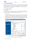
1. Launch Quartus II and select File->New Project Wizard to create a new project, as shown in
Figure 1-1 and Figure 1-2.
MAX10 Neek My
NiosII Manual
1
www.terasic.com
July 16, 2015
Figure 1-1 Select File -> New Project Wizard in Quartus II
MAX10 Neek My
NiosII Manual
2
www.terasic.com
July 16, 2015
Figure 1-2 First page of the New Project Wizard
2. Choose a working directory for this project. Enter the project name and top-level entity name, as
shown in Figure 1-3. Click Next and a window will pop up, as shown in Figure 1-4.
MAX10 Neek My
NiosII Manual
3
www.terasic.com
July 16, 2015
Figure 1-3 Define the working directory, project name, and top-level design entity name
MAX10 Neek My
NiosII Manual
4
www.terasic.com
July 16, 2015
Figure 1-4 Add Files
3. Click Next and choose the device family with device settings according to Figure 1-5. Click
Next to the next window, as shown in Figure 1-6.
MAX10 Neek My
NiosII Manual
5
www.terasic.com
July 16, 2015
Figure 1-5 Family & Device Settings
MAX10 Neek My
NiosII Manual
6
www.terasic.com
July 16, 2015
Figure 1-6 EDA Tool Settings
4. Click Next and a summary about the project which has just been created is shown in Figure 1-7.
Click Finish to complete the creation of a new project, as shown in Figure 1-8.
MAX10 Neek My
NiosII Manual
7
www.terasic.com
July 16, 2015
Figure 1-7 Summary of the new project
MAX10 Neek My
NiosII Manual
8
www.terasic.com
July 16, 2015
Figure 1-8 The new project in Quartus II
5. Choose Tools -> Qsys to open the Qsys system builder tool, as shown in Figure 1-9. Choose
File- > New System to create a new Qsys system, as shown in Figure 1-10.
MAX10 Neek My
NiosII Manual
9
www.terasic.com
July 16, 2015
Figure 1-9 Select Tool -> Qsys
MAX10 Neek My
NiosII Manual
10
www.terasic.com
July 16, 2015
Figure 1-10 Create a new Qsys system
6. Choose File -> Save and enter “NEEK10_QSYS.qsys”, as shown in Figure 1-11 and Figure
1-12.
MAX10 Neek My
NiosII Manual
11
www.terasic.com
July 16, 2015
Figure 1-11 Select File -> Save in Qsys
Figure 1-12 Enter“NEEK10_QSYS.qsys” as the file name
7. Right-click the clk_0 component and rename it to clk_50. Double click clk_50 to set the clock
frequency to 50000000 Hz, as shown in Figure 1-13.
MAX10 Neek My
NiosII Manual
12
www.terasic.com
July 16, 2015
Figure 1-13 Rename the clock source and set it to 50000000 Hz
8. Choose Library -> Processors and Peripherals- > Embedded Processors -> Nios II Processor
to add a Nios II processor into the system, as shown in Figure 1-14 and Figure 1-15.
Figure 1-14 Add Nios II Processor
MAX10 Neek My
NiosII Manual
13
www.terasic.com
July 16, 2015
Figure 1-15 Settings of Nios II Processor
9. Click Finish to return to the main window, as shown in Figure 1-16.
Figure 1-16 Complete adding Nios II processor
10. Right-click on nios2_gen2_0 and choose rename, as shown in Figure 1-17. Rename the Nios II
processor to cpu. Connect its clk and reset to the clk and clk_reset of clk_50, as shown in Figure
1-18.
MAX10 Neek My
NiosII Manual
14
www.terasic.com
July 16, 2015
Figure 1-17 Rename the Nios II processor
Figure 1-18 Establish the connection of clk and reset
11. Choose Library -> Interface Protocols -> Serial -> JTAG UART to add JTAG UART and
click Finish, as shown in Figure 1-19 and Figure 1-20.
MAX10 Neek My
NiosII Manual
15
www.terasic.com
July 16, 2015
Figure 1-19 Add JTAG UART
MAX10 Neek My
NiosII Manual
16
www.terasic.com
July 16, 2015
Figure 1-20 Settings of JTAG UART
12. Rename jtag_uart_0 to jtag_uart. Connect its clk and reset to the clk and clk_reset of clk_50,
respectively. Its avalon_jtag_slave is connected to the data_master of cpu. Figure 1-21 shows the
complete connections.
MAX10 Neek My
NiosII Manual
17
www.terasic.com
July 16, 2015
Figure 1-21 Rename JTAG UART
13. Choose Library -> Basic Functions -> On-Chip Memory-> On-Chip Memory (RAM or
ROM) to add On-Chip memory, as shown in Figure 1-22 and Figure 1-23.
MAX10 Neek My
NiosII Manual
18
www.terasic.com
July 16, 2015
Figure 1-22 Add On-Chip Memory
MAX10 Neek My
NiosII Manual
19
www.terasic.com
July 16, 2015
Figure 1-23 On-Chip Memory Box
16. Modify Total memory size to 102400 and uncheck “initialize memory content”, as shown in
Figure 1-24. Click Finish to return to the window as in Figure 1-25.
MAX10 Neek My
NiosII Manual
20
www.terasic.com
July 16, 2015
Figure 1-24 Update the default settings of On-Chip Memory
17. Rename onchip_memory2_0 to onchip_memory2. Connect its clk1 and reset1 to the clk and
clk_reset of clk_50. Its s1 is connected to the data_master and instruction_master of cpu. Figure
1-25 shows the complete connections.
MAX10 Neek My
NiosII Manual
21
www.terasic.com
July 16, 2015
Figure 1-25 Rename the On-Chip Memory and establish connections via nodes
18. Click cpu from the component list on the right to edit its settings. Click the Vectors tab to
update Reset vector and Exception Vector, as shown in Figure 1-26, and click Finish.
MAX10 Neek My
NiosII Manual
22
www.terasic.com
July 16, 2015
Figure 1-26 Update the settings of Nios II processor
19. Choose Library -> Processors and Peripherals -> Peripherals ->PIO (Parallel I/O) to open
add PIO component, as shown in Figure 1-27. Set the Width to 10 bits and click Finish, as shown
in Figure 1-28.
MAX10 Neek My
NiosII Manual
23
www.terasic.com
July 16, 2015
Figure 1-27 Add PIO component
MAX10 Neek My
NiosII Manual
24
www.terasic.com
July 16, 2015
Figure 1-28 Set the Width to 10 bits
21. Rename pio_0 to pio_led and connect its clk and reset to the clk and clk_reset of clk_50. Its s1
is connected to the data_master of cpu, reset to clk_reset of clk_50. Double click the Export column
of external_connection to export the signal “pio_led_external_connection”. Figure 1-29 shows the
complete connections and changes.
MAX10 Neek My
NiosII Manual
25
www.terasic.com
July 16, 2015
Figure 1-29 Connections and changes of PIO
22. Choose System -> Assign Base Addresses, as shown in Figure 1-30. The base addresses will
be assigned automatically and there should be no more error or warning message, as shown in
Figure 1-31.
MAX10 Neek My
NiosII Manual
26
www.terasic.com
July 16, 2015
Figure 1-30 Assign base addresses automatically
Figure 1-31 No more errors or warnings
MAX10 Neek My
NiosII Manual
27
www.terasic.com
July 16, 2015
23. Click Generate HDL… button on the bottom right corner and a window will pop up, as shown
in Figure 1-32. Click Generate button and the process will begin, as shown in Figure 1-33. Figure
1-34 shows there is no error message during the process.
Figure 1-32 Generate HDL files in Qsys
Figure 1-33 Generation process
MAX10 Neek My
NiosII Manual
28
www.terasic.com
July 16, 2015
Figure 1-34 Generation is complete and successful
25. Choose File -> New to open the dialogue and be prepared to add new files, as shown in Figure
1-35 and Figure 1-36.
MAX10 Neek My
NiosII Manual
29
www.terasic.com
July 16, 2015
Figure 1-35 Select File -> New
MAX10 Neek My
NiosII Manual
30
www.terasic.com
July 16, 2015
Figure 1-36 Add new Verilog HDL File
33. Select Verilog HDL File and click OK to finish creating a blank .v file, as shown in Figure
1-37.
MAX10 Neek My
NiosII Manual
31
www.terasic.com
July 16, 2015
Figure 1-37 A blank Verilog HDL file
34. Type in the following codes, as shown in Figure 1-38. The module NEEK10_QSYS comes
from NEEK10_QSYS.v, which is generated in Qsys. Figure 1-39 shows the contents of
NEEK10_QSYS.v.
module my_first_niosii
(
CLOCK_50,
LEDR
);
input
CLOCK_50;
output [9:0]
LEDR;
NEEK10_QSYS u0
(
.clk_50
. reset_reset_n
. pio_led_external_connection_export
);
endmodule
MAX10 Neek My
NiosII Manual
(CLOCK_50),
(1'b1),
(LEDR)
32
www.terasic.com
July 16, 2015
Figure 1-38 Input verilog Text
Figure 1-39 The module NEEK10_QSYS generated in Qsys
MAX10 Neek My
NiosII Manual
33
www.terasic.com
July 16, 2015
35. Choose File -> Save and save the Verilog HDL file as my_first_niosii.v, as shown in Figure
1-40.
Figure 1-40 Save the Verilog HDL file
36. Choose Project-> Add/Remove Files in Project and select NEEK10_QSYS.qip, as shown in
Figure 1-40. Click Add and then OK, as shown in Figure 1-40.
MAX10 Neek My
NiosII Manual
34
www.terasic.com
July 16, 2015
Figure 1-41 Choose NEEK10_QSYS.qsys
Figure 1-42 Add NEEK10_QSYS.qip
MAX10 Neek My
NiosII Manual
35
www.terasic.com
July 16, 2015
37. Choose Processing > Start Compilation, as shown in Figure 1-43. Figure 1-44 shows the
compilation is successful.
Figure 1-43 Start Compilation
Figure 1-44 Project is compiled successfully
39. Choose Assignments -> Pin Planner to open the pin planner, as shown in Figure 1-45. Figure
MAX10 Neek My
NiosII Manual
36
www.terasic.com
July 16, 2015
1-46 shows the blank pins.
Figure 1-45 Open the Pin Planner
Figure 1-46 Blank Pins
40. Input Location and IO Standard value for these plan pins, as shown in Figure 1-47.
Figure 1-47 Set Pins
41. Close the pin planner and re-compile the project.
MAX10 Neek My
NiosII Manual
37
www.terasic.com
July 16, 2015
1. 3 Download Har dware Design to MAX10 NEEK
Board
This section describes how to download the configuration file i.e the SRAM Object File (.sof)
which contains the Nios II standard system to the board. The steps are:
1. Connect the board to the host PC via the USB download cable.
2. Connect the power adaptor to the board and turn it on.
3. Choose Tools-> Programmer in Quartus II.
4. Click Hardware Setup on the top left comer of the Quartus II programmer window and a
Hardware Setup dialog box will appear.
5. Select NEEK10[USB-1] from the Currently selected hardware drop-down list box, as shown in
Figure 1-48. Click Close.
Note: If the hardware NEEK10[USB-1] does not appear in the list, it is likely the driver has not
been installed. Please refer to Quartus II Help on how to install the driver.
Figure 1-48 Hardware Setup
MAX10 Neek My
NiosII Manual
38
www.terasic.com
July 16, 2015
6. Click Auto Detect on the right column and the device onboard should be detected automatically.
7. Choose 10M50DAES and click OK, as shown in Figure 1-49.
Figure 1-49 Select Device
8. Right-click on the device and select Change File, as shown in Figure 1-50.
Figure 1-50 Change File
9. Browse to the project directory \ my_first_niosii.
10. Select the programming file i.e. myfirst_niosii.sof, as shown in Figure 1-51.
MAX10 Neek My
NiosII Manual
39
www.terasic.com
July 16, 2015
Figure 1-51 Select the programming file
12. Click the Program/Configure option, as shown in Figure 1-52.
Figure 1-52 Prepare to program myfirst_niosii.sof in Quartus II programmer
MAX10 Neek My
NiosII Manual
40
www.terasic.com
July 16, 2015
13. Click Start and wait for the Progress meter reaches 100%. When configuration is complete, the
FPGA is configured with the Nios II system, but it does not yet have a C program in memory to
execute.
MAX10 Neek My
NiosII Manual
41
www.terasic.com
July 16, 2015
Chapter 2
NIOS II Software Build Tools for
Eclipse
This chapter lists the steps to build Nios II software program in C code and compile the project to
run on the Nios II standard system from previous chapter on the MAX10 NEEK board. Users will
also learn how to edit the project, re-build it, and setup a debug session. The Nios II Software Build
Tools (SBT) for Eclipse is a graphical user interface (GUI) which automates build and makefile
management. The Nios II SBT for Eclipse integrates a text editor, debugger, the BSP editor, the
Nios II Flash programmer, and the Quartus II programmer. The example software application
templates included make it easy for new software programmers to get started quickly.
2. 1 Create the hello_wor ld Example Project
This section describes how to create a new NIOS II C/C++ application project based on an example
which comes with the installation of Nios II SBT. Please follow the steps below in Nios II SBT for
Eclipse:
1. Choose Tools->Nios II Software Build Tools for Eclipse in QuartusII software.
2. Select a workspace and click OK, as shown in Figure 2-1.
MAX10 Neek My
NiosII Manual
42
www.terasic.com
July 16, 2015
Figure 2-1 Select a workspace in Nios II SBT
3. Choose File->New->NIOS II Application and BSP from Template from Nios II SBT to open
the wizard for New Project .
4. There are three actions to be performed, as shown in Figure 2-2.
Browse to the target hardware system NEEK10_QSYS.sopcinfo under Target hardware
information.
Enter the project name my_first_niosii.
Select the Hello World project template.
MAX10 Neek My
NiosII Manual
43
www.terasic.com
July 16, 2015
Figure 2-2 Select project template to start creating a new project
5. Click Finish and the Nios II SBT for Eclipse will create a project named my_first_niosii, as
shown in Figure 2-3.
MAX10 Neek My
NiosII Manual
44
www.terasic.com
July 16, 2015
Figure 2-3 Project named my_first_niosii is created
There are two new projects created in Nios II SBT for Eclipse and shown in Poject Explorer on the
right:
■ my_first_niosii is the C/C++ application project. This project contains the source code and
header files for users’ application.
■ my_first_niosii_bsp is a board support package which encapsulates the details of the Nios II
system hardware.
Note: When a system library for the first time, the Nios II SBT for Eclipse will automatically
generates the following files for software development:
● Installed IP device drivers, which includes SOPC component device drivers for the NIOS II
hardware system.
● Newlib C library, which is a richly featured C library for the Nios II processor.
● Nios II software packages which include NIOS II hardware abstraction layer, NicheStack TCP/IP
Network stack, Nios II host file system, Nios II read-only zip file system, and Micrium’s μC/OS-II
MAX10 Neek My
NiosII Manual
45
www.terasic.com
July 16, 2015
real time operating system (RTOS).
● system.h, which is a header file that encapsulates the hardware system.
● alt_sys_init.c, which is a file that initializes the devices in the system.
●my_first_niosii.elf, which is an executable and linked format file for the application located in
my_first_niosii folder under Debug.
2. 2 Build and Run the Program
This section you describes how to build and run the program to execute the compiled code. The
steps are:
1. Right-click the project my_first_niosii in Project Exploror and choose Build Project. The
Build Project dialog box will appear and the Eclipse will start compiling the project.
2. When the compilation is successful, a message [my_first_niosii build complete] will appear
in the Console window, as shown in Figure 2-4. The compilation time depends on users’
system.
MAX10 Neek My
NiosII Manual
46
www.terasic.com
July 16, 2015
Figure 2-4 The build of my_first_niosii is complete
3. After compilation is complete, right-click the my_first_niosii project and choose Run As ->
NIOS II Hardware. The Eclipse will begin to download the program to the MAX10 NEEK
board. When the target hardware executes the program, a message 'Hello from Nios II!' will
appear in the Nios II Console window, as shown in Figure 2-5.
MAX10 Neek My
NiosII Manual
47
www.terasic.com
July 16, 2015
Figure 2-5 Niso II Console display program output
2. 3 Edit and Re-Run the Program
Users can modify the hello_world.c program file in the Eclipse, build it, and re-run the program to
observe the changes on the target board. This section shows how to make LEDR blink.
Please follow the steps below to modify and re-run the program:
1. In the hello_world.c file, add the lines of code in blue accordingly.
#include <stdio.h>
#include "system.h"
#include "altera_avalon_pio_regs.h"
int main()
{
MAX10 Neek My
NiosII Manual
48
www.terasic.com
July 16, 2015
printf("Hello from Nios II!\n");
int count = 0;
int delay;
while(1)
{
IOWR_ALTERA_AVALON_PIO_DATA(PIO_LED_BASE, count & 0x01);
delay = 0;
while(delay < 2000000)
{
delay++;
}
count++;
}
return 0;
}
2. Save the project and re-compile the file by right-clicking my_first_niosii in the NIOS II C/C++
Projects tab and choosing Run -> Run As -> Nios II Hardware.
Note: Users do not need to build the project manually, as the Nios II Eclipse automatically re-builds
the program before downloading it to the target board.
4. Orient the MAX10 NEEK board to observe LEDR blinking.
2. 4 W hy the LED Blinks
The Nios II system description header file, system.h, contains the software definitions, name,
locations, base addresses, and settings for all components in the Nios II hardware system. The
system.h file is located in the directory my_first_niosii_bsp, as shown in Figure 2-6.
MAX10 Neek My
NiosII Manual
49
www.terasic.com
July 16, 2015
Figure 2-6 The location of system.h
The key part of system.h file for the Nios II project example used in this tutorial is pio_led. This
function controls the LED and the Nios II processor controls the PIO ports, which are connected to
the LEDs, by reading and writing to the register map. For the PIO, there are four registers: data,
direction, interrupt mask, and edge capture. The data register of PIO needs to be written to turn
on and off the LEDs.
The PIO core has an associated software file altera_avalon_pio_regs.h. This file defines the core’s
register map, providing symbolic constants to access the low-level hardware.
The altera_avalon_pio_regs.h
file is located in altera\<version number>\ip\altera\sopc_builder_ip\altera_avalon_pio.
When the altera_avalon_pio_regs.h file is included, several useful functions become available to
access the PIO core registers, especially the function
IOWR_ALTERA_AVALON_PIO_DATA (base, data)
It can write to the PIO data register to turn the LED on and off. For more information about the PIO
core and other embedded peripheral cores, please refer to Quartus II Version <version> Handbook
MAX10 Neek My
NiosII Manual
50
www.terasic.com
July 16, 2015
Volume 5: Embedded Peripherals.
When developing your own designs, you can use the software functions and resources that are
provided with the Nios II HAL. Refer to the Nios II Software Developer’s Handbook for extensive
documentation on developing your own Nios II processor-based software applications.
2. 5 Setup Debug Configuration
A debug configuration which specifies how to run the software needs to be created before users can
debug a project in Nios II SBT for Eclipse. The steps to setup a debug configuration are:
1. Set a breakpoint by double clicking the front of which line to be observed in hello_world.c, as
shown in Figure 2-7.
Figure 2-7 Set a breakpoint
2. Right-click the application i.e. my_first_niosii and choose Debug as > Nios II Hardware to
start the process.
MAX10 Neek My
NiosII Manual
51
www.terasic.com
July 16, 2015
3. If a Confirm Perspective Switch message box appears, click Yes.
4. The main () function should appear in the editor shortly. A blue arrow next to the first line of code
indicates the execution stops at the line.
5. Choose Run-> Resume to continue execution.
When debugging a project in the Nios II SBT for Eclipse, users can pause, stop or single step the
program. Users can also set breakpoints, examine variables, or perform other common debugging
tasks.
Note: To return to the Nios II C/C++ project perspective from the debug perspective, click the icon
with two arrows >> on the top right corner.
2. 6 Configure System Librar y
This section describes how to configure some advanced options about the target memory or other
things. All the available settings can be changed by following the steps below:
By performing the following steps, you can change all the available settings:
1. Right-click my_first_niosii_bsp in Nios II SBT for Eclipse and choose Nios II-> BSP
Editor.
2. The Main page contains settings related to how the program interacts with the underlying
hardware. The settings have names which correspond to the targeted Nios II hardware.
3. Observe which memory has been assigned for Program memory(.text), Read-only data
memory(.rodata), Read/write data memory(.rwdata), Heap memory, and Stack memory in the
Linker Script box, as shown in Figure 2-7. These settings determine which memory is used to store
the compiled executable program when running the my_first_niosii program. Users can specify
which interface to be used for stdio , stdin, and stderr. Users can also add and configure a RTOS for
users’ application and configure build options to support C++ or reduced device drivers, etc.
4. Choose onchip_memory2 for all the memory options in the Linker Script box, as shown in
Figure 2-8.
MAX10 Neek My
NiosII Manual
52
www.terasic.com
July 16, 2015
Figure 2-8 Configure BSP
5. Click Generate then Exit to close the BSP Editor dialog box and return to the Eclipse
workbench.
Note: If users make changes to the system properties or the Qsys properties or the hardware, the
project must be rebuilt by right-clicking my_first_niosii_bsp ->Nios II ->Generate BSP ->
ReBuild Project.
MAX10 Neek My
NiosII Manual
53
www.terasic.com
July 16, 2015
Chapter 3
Program and Boot On-chip Flash
This chapter describes how to program and boot the on-chip Flash in MAX 10 device. The Nios II
soft core process is configured to execute the code from the on-chip memory using Altera On-chip
Flash IP core.
3.1 Modify Project in Qsys
1. Choose Library -> Basic Functions-> On Chip Memory ->Altera On-Chip Flash, as shown
in Figure 3-1. Set Configuration Mode to Single Uncompressed Image and make sure the Initialize
flash content option is left unchecked, as shown in Figure 3-2. Click Finish.
Figure 3-1 Add Altera On-Chip Flash in Qsys
MAX10 Neek My
NiosII Manual
54
www.terasic.com
July 16, 2015
Figure 3-2
Settings of Altera On-Chip Flash
2. Choose onchip_flash_0 and rename it to onchip_flash. Connect its clk and nreset to the clk and
clk_reset of of clk_50, respectively. Its data is connected to the data_master and instruction_master
of cpu and its csr is connected to the data_master of the cpu. Figure 3-3 shows the complete
connections.
MAX10 Neek My
NiosII Manual
55
www.terasic.com
July 16, 2015
Figure 3-3
Rename onchip_flash and establish connections
3. Double click cpu to edit the Nios II Processor component. Change Reset vector to onchip_flash.data as
shown in Figure 3-4.
MAX10 Neek My
NiosII Manual
56
www.terasic.com
July 16, 2015
Figure 3-4 Change Reset Vector
4. Choose System -> Assign Base Addresses and click Generate ->Generate HDL to generate the
HDL files in Qsys, as shown in Figure 3-5.
Figure 3-5 Generate HDL files in Qsys
MAX10 Neek My
NiosII Manual
57
www.terasic.com
July 16, 2015
5. Open Quartus II and select Assignment -> Device -> Device and Pin Options -> Configuration.
Set Configuration mode to Single Uncompressed Image (3584Kbits UFM), as shown in Figure 3-6.
Click OK twice to exit the window.
Figure 3-6 Set the Configuration mode
6. Re-compile my_first_niosii project
3.2 Reconfigure Nios II BSP Editor
1. Right-click my_first_niosii_bsp in Nios II SBT for Eclipse and choose Nios II ->Generate BSP,
as shown in Figure 3-7.
MAX10 Neek My
NiosII Manual
58
www.terasic.com
July 16, 2015
Figure 3-7 Generate BSP
2. Right-click my_first_niosii_bsp and choose Nios II -> BSP Editor, as shown in Figure 3-8.
Figure 3-8 Choose BSP Editor
3. Go to Settings-> Advanced ->linker to expand the list and set the options of hal.linker according
to Figure 3-9.
MAX10 Neek My
NiosII Manual
59
www.terasic.com
July 16, 2015
Figure 3-9 Set the options of hal.linker
4. Click on the Linker Script tab in Nios II BSP Editor. Set the .text item in the Linker Section
Name to the Altera On-chip Flash in the Linker Region Name. Set the rest of the items in the Linker
Section Name list to Altera On-chip RAM, as shown in Figure 3-10.
MAX10 Neek My
NiosII Manual
60
www.terasic.com
July 16, 2015
Figure 3-10
Setup the Linker Script
5. Click Generate and then Exit.
6. Right-click on my_first_niosii in Nios II SBT tool and click Make Targets -> Build…, as
shown in Figure 3-11. Select mem_init_generate and click Build to generate the HEX file.
MAX10 Neek My
NiosII Manual
61
www.terasic.com
July 16, 2015
Figure 3-11 Generate the HEX file
3.3 Programming On-chip Flash
1. Click File->Convert Programming Files in Quartus II, as shown in Figure 3-12.
MAX10 Neek My
NiosII Manual
62
www.terasic.com
July 16, 2015
Figure 3-12
Open the programming file to be converted
2. Set Programming file type to Programmer Object File(.pof) and Mode to Internal
Configuration, as shown in Figure 3-13.
MAX10 Neek My
NiosII Manual
63
www.terasic.com
July 16, 2015
Figure 3-13 Settings of Convert Programming File
3. Click Options/Boot info..., and the dialog of MAX 10 Device Options will appear. Choose
Load memory file for UFM source and browse to the generated Altera On-chip Flash HEX file
(onchip_flash.hex) in the File path, as shown in Figure 3-14. Click OK.
MAX10 Neek My
NiosII Manual
64
www.terasic.com
July 16, 2015
Figure 3-14
Set Load memory file as UFM source
4. Click Add File from the Input files to convert section and point to the generated Quartus II .sof
file my_first_niosii.sof, as shown in Figure 3-15. Click Generate to create the .pof file, as shown
in Figure 3-16.
MAX10 Neek My
NiosII Manual
65
www.terasic.com
July 16, 2015
Figure 3-15
Figure 3-16
Select my_first_niosii.sof
Click Generate to create the .pof file
5. Choose Tools> Programmer in Quartus II and click Hardware Setup. Choose Neek10[USB-1]
MAX10 Neek My
NiosII Manual
66
www.terasic.com
July 16, 2015
and click Add File. Choose output_file.pof, as shown in Figure 3-17.
Figure 3-17 Choose output_file.pof file
6. Check the Program/Configure option in Programmer for output_file.pof .Click Start to begin
the programming, as shown in Figure 3-18.
MAX10 Neek My
NiosII Manual
67
www.terasic.com
July 16, 2015
Figure 3-18 Program output_file.pof
7. Turn off the board and turn it on again. The LEDs should be blinking.
MAX10 Neek My
NiosII Manual
68
www.terasic.com
July 16, 2015