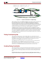
1
Xilinx Timing
Constraints
User Guide
UG612 (v1.0.0) December 9, 2008
R
R
Xilinx is disclosing this user guide, manual, release note, and/or specification (the "Documentation") to you solely for use in the development
of designs to operate with Xilinx hardware devices. You may not reproduce, distribute, republish, download, display, post, or transmit the
Documentation in any form or by any means including, but not limited to, electronic, mechanical, photocopying, recording, or otherwise,
without the prior written consent of Xilinx. Xilinx expressly disclaims any liability arising out of your use of the Documentation. Xilinx reserves
the right, at its sole discretion, to change the Documentation without notice at any time. Xilinx assumes no obligation to correct any errors
contained in the Documentation, or to advise you of any corrections or updates. Xilinx expressly disclaims any liability in connection with
technical support or assistance that may be provided to you in connection with the Information.
THE DOCUMENTATION IS DISCLOSED TO YOU “AS-IS” WITH NO WARRANTY OF ANY KIND. XILINX MAKES NO OTHER
WARRANTIES, WHETHER EXPRESS, IMPLIED, OR STATUTORY, REGARDING THE DOCUMENTATION, INCLUDING ANY
WARRANTIES OF MERCHANTABILITY, FITNESS FOR A PARTICULAR PURPOSE, OR NONINFRINGEMENT OF THIRD-PARTY
RIGHTS. IN NO EVENT WILL XILINX BE LIABLE FOR ANY CONSEQUENTIAL, INDIRECT, EXEMPLARY, SPECIAL, OR INCIDENTAL
DAMAGES, INCLUDING ANY LOSS OF DATA OR LOST PROFITS, ARISING FROM YOUR USE OF THE DOCUMENTATION.
© 2002–2008 Xilinx, Inc. All rights reserved.
XILINX, the Xilinx logo, the Brand Window, and other designated brands included herein are trademarks of Xilinx, Inc. All other trademarks
are the property of their respective owners
www.xilinx.com
Preface: About the Xilinx Timing Constraints User Guide
Xilinx Timing Constraints User Guide Contents . . . . . . . . . . . . . . . . . . . . . . . . . . . . . . 3
Additional Resources . . . . . . . . . . . . . . . . . . . . . . . . . . . . . . . . . . . . . . . . . . . . . . . . . . . . . . . . 3
Conventions . . . . . . . . . . . . . . . . . . . . . . . . . . . . . . . . . . . . . . . . . . . . . . . . . . . . . . . . . . . . . . . . . 3
Typographical . . . . . . . . . . . . . . . . . . . . . . . . . . . . . . . . . . . . . . . . . . . . . . . . . . . . . . . . . . . . . 4
Online Document . . . . . . . . . . . . . . . . . . . . . . . . . . . . . . . . . . . . . . . . . . . . . . . . . . . . . . . . . . 4
Chapter 1: Introduction to the Xilinx Timing Constraints User Guide
Chapter 2: Timing Constraint Methodology
About Timing Constraint Methodology . . . . . . . . . . . . . . . . . . . . . . . . . . . . . . . . . . . . . . 9
Basic Constraints Methodology . . . . . . . . . . . . . . . . . . . . . . . . . . . . . . . . . . . . . . . . . . . . . . 10
Input Timing Constraints . . . . . . . . . . . . . . . . . . . . . . . . . . . . . . . . . . . . . . . . . . . . . . . . . . . 10
About Input Timing Constraints . . . . . . . . . . . . . . . . . . . . . . . . . . . . . . . . . . . . . . . . . . . . 11
System Synchronous Inputs . . . . . . . . . . . . . . . . . . . . . . . . . . . . . . . . . . . . . . . . . . . . . . . . 11
Source Synchronous Inputs . . . . . . . . . . . . . . . . . . . . . . . . . . . . . . . . . . . . . . . . . . . . . . . . 12
Register-To-Register Timing Constraints . . . . . . . . . . . . . . . . . . . . . . . . . . . . . . . . . . . . 14
About Register-To-Register Timing Constraints . . . . . . . . . . . . . . . . . . . . . . . . . . . . . . .
Automatically Related Synchronous DCM/PLL Clock Domains . . . . . . . . . . . . . . . .
Manually Related Synchronous Clock Domains . . . . . . . . . . . . . . . . . . . . . . . . . . . . . . .
Asynchronous Clock Domains. . . . . . . . . . . . . . . . . . . . . . . . . . . . . . . . . . . . . . . . . . . . . .
14
15
15
17
Output Timing Constraints . . . . . . . . . . . . . . . . . . . . . . . . . . . . . . . . . . . . . . . . . . . . . . . . . . 18
System Synchronous Output . . . . . . . . . . . . . . . . . . . . . . . . . . . . . . . . . . . . . . . . . . . . . . . 18
Source Synchronous Outputs . . . . . . . . . . . . . . . . . . . . . . . . . . . . . . . . . . . . . . . . . . . . . . . 20
Timing Exceptions . . . . . . . . . . . . . . . . . . . . . . . . . . . . . . . . . . . . . . . . . . . . . . . . . . . . . . . . . . 21
False Paths . . . . . . . . . . . . . . . . . . . . . . . . . . . . . . . . . . . . . . . . . . . . . . . . . . . . . . . . . . . . . . . 22
Multi-Cycle Paths . . . . . . . . . . . . . . . . . . . . . . . . . . . . . . . . . . . . . . . . . . . . . . . . . . . . . . . . . 22
Chapter 3: Timing Constraint Principles
Constraint System . . . . . . . . . . . . . . . . . . . . . . . . . . . . . . . . . . . . . . . . . . . . . . . . . . . . . . . . . . . 25
About the Constraint System . . . . . . . . . . . . . . . . . . . . . . . . . . . . . . . . . . . . . . . . . . . . . . .
DLL/DCM/PLL/BUFR/PMCD Components . . . . . . . . . . . . . . . . . . . . . . . . . . . . . . . .
About DLL/DCM/PLL/BUFR/PMCD Components . . . . . . . . . . . . . . . . . . . . . . . . . .
Transformation Conditions . . . . . . . . . . . . . . . . . . . . . . . . . . . . . . . . . . . . . . . . . . . . . . .
New PERIOD Constraints on DCM Outputs . . . . . . . . . . . . . . . . . . . . . . . . . . . . . . . . .
Synchronous Elements . . . . . . . . . . . . . . . . . . . . . . . . . . . . . . . . . . . . . . . . . . . . . . . . . .
Analysis with NET PERIOD . . . . . . . . . . . . . . . . . . . . . . . . . . . . . . . . . . . . . . . . . . . . . .
PHASE Keyword . . . . . . . . . . . . . . . . . . . . . . . . . . . . . . . . . . . . . . . . . . . . . . . . . . . . . .
DLL/DCM/PLL Manipulation with PHASE . . . . . . . . . . . . . . . . . . . . . . . . . . . . . . . . .
Timing Group Creation with TNM/TNM_NET Attributes . . . . . . . . . . . . . . . . . . . . .
About Timing Group Creation with TNM/TNM_NET Attributes . . . . . . . . . . . . . . . . .
Net Connectivity (NET) . . . . . . . . . . . . . . . . . . . . . . . . . . . . . . . . . . . . . . . . . . . . . . . . .
Predefined Time Groups . . . . . . . . . . . . . . . . . . . . . . . . . . . . . . . . . . . . . . . . . . . . . . . . .
Propagation Rules for TNM_NET. . . . . . . . . . . . . . . . . . . . . . . . . . . . . . . . . . . . . . . . . .
Instance or Hierarchy . . . . . . . . . . . . . . . . . . . . . . . . . . . . . . . . . . . . . . . . . . . . . . . . . . .
Instance Pin . . . . . . . . . . . . . . . . . . . . . . . . . . . . . . . . . . . . . . . . . . . . . . . . . . . . . . . . . . .
Grouping Constraints . . . . . . . . . . . . . . . . . . . . . . . . . . . . . . . . . . . . . . . . . . . . . . . . . . . . .
Pattern Matching . . . . . . . . . . . . . . . . . . . . . . . . . . . . . . . . . . . . . . . . . . . . . . . . . . . . . .
Time Group Examples . . . . . . . . . . . . . . . . . . . . . . . . . . . . . . . . . . . . . . . . . . . . . . . . . .
Xilinx Timing Constraints User Guide
UG612 (v1.0.0) December 5, 2008
www.xilinx.com
25
26
26
27
27
28
29
29
29
30
30
31
32
33
34
38
39
40
41
1
Constraint Priorities . . . . . . . . . . . . . . . . . . . . . . . . . . . . . . . . . . . . . . . . . . . . . . . . . . . . . . . . . 43
Timing Constraints . . . . . . . . . . . . . . . . . . . . . . . . . . . . . . . . . . . . . . . . . . . . . . . . . . . . . . . . . 44
About Timing Constraints . . . . . . . . . . . . . . . . . . . . . . . . . . . . . . . . . . . . . . . . . . . . . . . . .
Timing Constraint Exceptions. . . . . . . . . . . . . . . . . . . . . . . . . . . . . . . . . . . . . . . . . . . . .
Setting Timing Constraint Requirements . . . . . . . . . . . . . . . . . . . . . . . . . . . . . . . . . . . .
PERIOD Constraints . . . . . . . . . . . . . . . . . . . . . . . . . . . . . . . . . . . . . . . . . . . . . . . . . . . . . .
About PERIOD Constraints . . . . . . . . . . . . . . . . . . . . . . . . . . . . . . . . . . . . . . . . . . . . . .
Related TIMESPEC PERIOD Constraints . . . . . . . . . . . . . . . . . . . . . . . . . . . . . . . . . . . .
Paths Covered by PERIOD Constraints . . . . . . . . . . . . . . . . . . . . . . . . . . . . . . . . . . . . .
OFFSET Constraints. . . . . . . . . . . . . . . . . . . . . . . . . . . . . . . . . . . . . . . . . . . . . . . . . . . . . . .
About OFFSET Constraints . . . . . . . . . . . . . . . . . . . . . . . . . . . . . . . . . . . . . . . . . . . . . . .
Paths Covered by OFFSET Constraints . . . . . . . . . . . . . . . . . . . . . . . . . . . . . . . . . . . . . .
FROM:TO (Multi-Cycle) Constraints . . . . . . . . . . . . . . . . . . . . . . . . . . . . . . . . . . . . . . . .
About FROM:TO (Multi-Cycle) Constraints . . . . . . . . . . . . . . . . . . . . . . . . . . . . . . . . . .
False Paths or Timing Ignore (TIG) Constraint . . . . . . . . . . . . . . . . . . . . . . . . . . . . . . . .
Paths Covered by FROM:TO Constraints . . . . . . . . . . . . . . . . . . . . . . . . . . . . . . . . . . . .
44
45
45
45
45
46
48
50
51
53
55
55
59
60
Timing Constraint Syntax . . . . . . . . . . . . . . . . . . . . . . . . . . . . . . . . . . . . . . . . . . . . . . . . . . . 61
Creating Timing Constraints . . . . . . . . . . . . . . . . . . . . . . . . . . . . . . . . . . . . . . . . . . . . . . . . 61
Timing Constraint Analysis . . . . . . . . . . . . . . . . . . . . . . . . . . . . . . . . . . . . . . . . . . . . . . . . . 62
About Timing Constraint Analysis . . . . . . . . . . . . . . . . . . . . . . . . . . . . . . . . . . . . . . . . . .
PERIOD Constraints . . . . . . . . . . . . . . . . . . . . . . . . . . . . . . . . . . . . . . . . . . . . . . . . . . . . . .
About PERIOD Constraints . . . . . . . . . . . . . . . . . . . . . . . . . . . . . . . . . . . . . . . . . . . . . .
Gated Clocks . . . . . . . . . . . . . . . . . . . . . . . . . . . . . . . . . . . . . . . . . . . . . . . . . . . . . . . . . .
Single Clock Domain . . . . . . . . . . . . . . . . . . . . . . . . . . . . . . . . . . . . . . . . . . . . . . . . . . .
Two-Phase Clock Domain. . . . . . . . . . . . . . . . . . . . . . . . . . . . . . . . . . . . . . . . . . . . . . . .
Multiple Clock Domains . . . . . . . . . . . . . . . . . . . . . . . . . . . . . . . . . . . . . . . . . . . . . . . . .
Clocks from DCM outputs . . . . . . . . . . . . . . . . . . . . . . . . . . . . . . . . . . . . . . . . . . . . . . .
Clk0 Clock Domain . . . . . . . . . . . . . . . . . . . . . . . . . . . . . . . . . . . . . . . . . . . . . . . . . . . . .
Clk90 Clock Domain . . . . . . . . . . . . . . . . . . . . . . . . . . . . . . . . . . . . . . . . . . . . . . . . . . . .
Clk2x Clock Domain . . . . . . . . . . . . . . . . . . . . . . . . . . . . . . . . . . . . . . . . . . . . . . . . . . . .
CLKDV/CLKFX Clock Domain . . . . . . . . . . . . . . . . . . . . . . . . . . . . . . . . . . . . . . . . . . .
FROM:TO (Multi-Cycle) Constraints . . . . . . . . . . . . . . . . . . . . . . . . . . . . . . . . . . . . . . . .
OFFSET IN Constraints . . . . . . . . . . . . . . . . . . . . . . . . . . . . . . . . . . . . . . . . . . . . . . . . . . . .
About OFFSET IN Constraints . . . . . . . . . . . . . . . . . . . . . . . . . . . . . . . . . . . . . . . . . . . .
OFFSET IN BEFORE Constraints . . . . . . . . . . . . . . . . . . . . . . . . . . . . . . . . . . . . . . . . . .
OFFSET IN AFTER Constraints . . . . . . . . . . . . . . . . . . . . . . . . . . . . . . . . . . . . . . . . . . .
OFFSET OUT Constraints . . . . . . . . . . . . . . . . . . . . . . . . . . . . . . . . . . . . . . . . . . . . . . . . . .
About OFFSET OUT Constraints . . . . . . . . . . . . . . . . . . . . . . . . . . . . . . . . . . . . . . . . . .
OFFSET OUT AFTER Constraints . . . . . . . . . . . . . . . . . . . . . . . . . . . . . . . . . . . . . . . . .
OFFSET OUT BEFORE Constraints . . . . . . . . . . . . . . . . . . . . . . . . . . . . . . . . . . . . . . . .
62
62
63
63
64
64
66
66
66
67
68
69
70
72
72
73
80
80
80
81
86
Clock Skew . . . . . . . . . . . . . . . . . . . . . . . . . . . . . . . . . . . . . . . . . . . . . . . . . . . . . . . . . . . . . . . . . 87
Clock Uncertainty . . . . . . . . . . . . . . . . . . . . . . . . . . . . . . . . . . . . . . . . . . . . . . . . . . . . . . . . . . . 90
Asynchronous Reset Paths . . . . . . . . . . . . . . . . . . . . . . . . . . . . . . . . . . . . . . . . . . . . . . . . . . 91
Xilinx Timing Constraints User Guide
UG612 (v1.0.0) December 5, 2008
www.xilinx.com
2
R
Preface
About the Xilinx Timing Constraints
User Guide
This chapter provides general information about this Guide, and includes:
•
“Xilinx Timing Constraints User Guide Contents”
•
“Additional Resources”
•
“Conventions”
Xilinx Timing Constraints User Guide Contents
The Xilinx Timing Constraints User Guide contains the following chapters:
•
Chapter 1, “Introduction to the Xilinx Timing Constraints User Guide”
•
Chapter 2, “Timing Constraint Methodology”
•
Chapter 3, “Timing Constraint Principles”
Additional Resources
For additional documentation, see the Xilinx website at:
http://www.xilinx.com/literature.
To search the Answer Database of silicon, software, and IP questions and answers, or to
create a technical support WebCase, see the Xilinx website at:
http://www.xilinx.com/support.
Conventions
This document uses the following conventions. An example illustrates each convention.
•
“Typographical”
•
“Online Document”
Xilinx Timing Constraints User Guide
UG612 (v1.0.0) December 5, 2008
www.xilinx.com
3
R
Preface: About the Xilinx Timing Constraints User Guide
Typographical
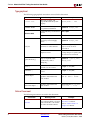
The following typographical conventions are used in this document:
Convention
Meaning or Use
Example
Courier font
Messages, prompts, and
program files that the system
displays
speed grade: - 100
Courier bold
Literal commands that you enter
in a syntactical statement
ngdbuild design_name
Commands that you select from
a menu
File > Open
Keyboard shortcuts
Ctrl+C
Variables in a syntax statement
for which you must supply
values
ngdbuild design_name
References to other manuals
See the Development System
Reference Guide for more
information.
Emphasis in text
If a wire is drawn so that it
overlaps the pin of a symbol, the
two nets are not connected.
Square brackets [ ]
An optional entry or parameter.
They are required in bus
specifications, such as
bus[7:0],
ngdbuild [option_name]
design_name
Braces { }
A list of items from which you
must choose one or more
lowpwr ={on|off}
Vertical bar |
Separates items in a list of
choices
lowpwr ={on|off}
Vertical ellipsis
.
.
.
Repetitive material that has
been omitted
IOB #1: Name = QOUT’
IOB #2: Name = CLKIN’
.
.
.
Horizontal ellipsis . . .
Repetitive material that has
been omitted
allow block block_name
loc1 loc2 ... locn;
Helvetica bold
Italic font
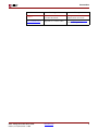
Online Document
The following conventions are used in this document:
Convention
Blue text
4
Meaning or Use
Example
Cross-reference link to a location
in the current file or in another
file in the current document
www.xilinx.com
See the section “Additional
Resources” for details.
Refer to “Title Formats” in
Chapter 1 for details.
Xilinx Timing Constraints User Guide
UG612 (v1.0.0) December 5, 2008
R
Conventions
Convention
Meaning or Use
Example
Red text
Cross-reference link to a location
in another document
See Figure 2-5 in the Virtex-II
Platform FPGA User Guide.
Blue, underlined text
Hyperlink to a website (URL)
Go to http://www.xilinx.com
for the latest speed files.
Xilinx Timing Constraints User Guide
UG612 (v1.0.0) December 5, 2008
www.xilinx.com
5
Preface: About the Xilinx Timing Constraints User Guide
6
www.xilinx.com
R
Xilinx Timing Constraints User Guide
UG612 (v1.0.0) December 5, 2008
R
Chapter 1
Introduction to the Xilinx Timing
Constraints User Guide
The Xilinx® Timing Constraints User Guide is written specifically to address timing closure
in high-performance applications. The guide is designed for all FPGA designers, from
beginners to advanced. The high performance of today's Xilinx devices can overcome the
speed limitations of other technologies and older devices. Designs that formerly only fit or
ran at high clock frequencies in an ASIC device are finding their way into Xilinx FPGA
devices. In addition, it is imperative that designers have a proven methodology for
obtaining their performance objectives.
This Guide discusses:
•
The fundamentals of timing constraints, including:
♦
“PERIOD Constraints”
♦
“OFFSET IN Constraints”
♦
“OFFSET OUT Constraints”
♦
“FROM:TO (Multi-Cycle) Constraints”
•
The ability to group elements and provided a better understanding of the constraint
system software
•
Information about the analysis of the basic constraints, with clock skew and clock
uncertainty
Xilinx Timing Constraints User Guide
UG612 (v1.0.0) December 5, 2008
www.xilinx.com
7
Chapter 1: Introduction to the Xilinx Timing Constraints User Guide
8
www.xilinx.com
R
Xilinx Timing Constraints User Guide
UG612 (v1.0.0) December 5, 2008
R
Chapter 2
Timing Constraint Methodology
This chapter discusses Timing Constraint Methodology, and includes:
•
“About Timing Constraint Methodology”
•
“Basic Constraints Methodology”
•
“Input Timing Constraints”
•
“Register-To-Register Timing Constraints”
•
“Output Timing Constraints”
•
“Timing Exceptions”
About Timing Constraint Methodology
You must have a proven methodology in order to meet your design objectives. This
chapter outlines the process to:
•
Understand the design requirements
•
Constrain the design to meet these requirements
Before starting a design, you must understand:
•
The performance requirements of the system
•
The features of the target device
This knowledge allows you to use proper coding techniques utilizing the features of the
device to give the best performance.
The FPGA device requirements depend on the system and the upstream and downstream
devices. Once the interfaces to the FPGA device are known, the internal requirements can
be outlined. How to meet these requirements depends on the device and its features.
You should understand:
•
The device clocking structure
•
RAM and DSP blocks
•
Any hard IP contained within the device
For more information, see the device User Guide.
Timing constraints communicate all design requirements to the implementation tools. This
also implies that all paths are covered by the appropriate constraint. This chapter provides
general guidelines that explain the strategy for identifying and constraining the most
common timing paths in FPGA devices as efficiently as possible.
Xlinx Timing Constraints User Guide
UG612 (v1.0.0) December 5, 2008
www.xilinx.com
9
R
Chapter 2: Timing Constraint Methodology
Basic Constraints Methodology
Timing requirements fall into into several global categories depending on the type of path
to be covered.
The most common types of path categories include:
•
Input paths
•
Synchronous element to synchronous element paths
•
Path specific exceptions
•
Output Paths
A Xilinx® timing constraint is associated with each of these global constraint types. The
most efficient way to specify these constraints is to begin with global constraints and add
path specific exceptions as needed. In many cases, only the global constraints are required.
The FPGA device implementation tools are driven by the specified timing requirements.
They assign device resources and expend the appropriate amount of effort necessary to
ensure the timing requirements are met. However, when a requirement is over-constrained
- or specified as a value greater than the design requirement - the effort spent by the tools
to meet this constraint increases significantly. This extra effort results in increased memory
use and tool runtime.
More importantly, over-constraint can result in loss of performance, not only for the
constraint in question, but for other constraints as well. For this reason, Xilinx recommends
that you specify the constraint values using the actual design requirements.
Xilinx recommends that you always comment the constraints file. This allows other
designers to understand why each constraint is used.
Include in your comments:
•
Source of the constraint
•
Whether the PERIOD constraint is based on an external clock
This Guide uses UCF constraint syntax examples. This format passes the design
requirements to the implementation tools. However, the easiest way to enter design
constraints is to use Constraints Editor.
Constraints Editor:
•
Provides a unified location in which to manage all the timing constraints associated
with a design
•
Provides assistance in creating timing constraints from the design requirements in
UCF syntax
Input Timing Constraints
This section discusses Input Timing Constraints and includes:
10
•
“About Input Timing Constraints”
•
“System Synchronous Inputs”
•
“Source Synchronous Inputs”
www.xilinx.com
Xlinx Timing Constraints User Guide
UG612 (v1.0.0) December 5, 2008
R
Input Timing Constraints
About Input Timing Constraints
Input timing covers the data path from the external pin of the FPGA device to the internal
register that captures that data. The constraint used to specify the input timing is the
OFFSET IN constraint. The best way to specify the input timing requirements depends on
the type (source/system synchronous) and single data rate (SDR) or double data rate
(DDR) of the interface.
The OFFSET IN constraint defines the relationship between the data and the clock edge
used to capture that data at the pins of the FPGA device. When analyzing the OFFSET IN
constraint, the timing analysis tools automatically take all internal factors affecting the
delay of the clock and data into account. These factors include:
•
Frequency and phase transformations of the clock
•
Clock uncertainties
•
Data delay adjustments
In addition to the automatic adjustments, you may also add additional input clock
uncertainty to the PERIOD constraint associated with the interface clock.
For more information on adding INPUT_JITTER, see “PERIOD Constraints” in Chapter 3,
“Timing Constraint Principles.”
The OFFSET IN constraint is associated with a single input clock. By default, the OFFSET
IN constraint covers all paths from the input pads of the FPGA device to the internal
synchronous elements that capture that data and are triggered by the specified OFFSET IN
clock. This application of the OFFSET IN constraint is called the global method. It is the
most efficient way to specify input timing.
System Synchronous Inputs
In a system synchronous interface, a common system clock both transfers and captures the
data. This interface uses a common system clock. The board trace delays and clock skew
limit the operating frequency of the interface. The lower frequency also results in the
system synchronous input interface typically being an SDR application.
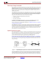
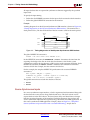
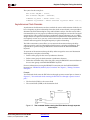
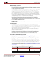
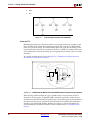
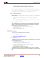
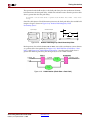
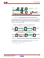
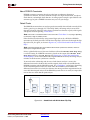
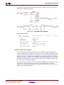
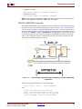
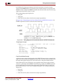
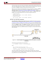
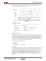
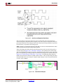
In the system synchronous SDR application example, shown in Figure 2-1, “Simplified
System Synchronous interface with associated SDR timing,” the data is transmitted from
the source device on one rising clock edge and captured in the FPGA device on the next
rising clock edge.
S our ce Devi ce
FP GA
Transmit
Edge
Dat a
D
Q
D
Captur e
Edge
Q
REG
REG
CL K
C LK
System Clock
Data
Data
S ys t em Clock
Figure 2-1:
Simplified System Synchronous interface with associated SDR timing
The global OFFSET IN constraint is the most efficient way to specify the input timing for a
system synchronous interface. In this method, one OFFSET IN constraint is defined for
each system synchronous input interface clock. This single constraint covers the paths of
Xlinx Timing Constraints User Guide
UG612 (v1.0.0) December 5, 2008
www.xilinx.com
11
R
Chapter 2: Timing Constraint Methodology
all input data bits that are captured in synchronous elements triggered by the specified
input clock.
To specify the input timing:
•
Define the clock PERIOD constraint for the input clock associated with the interface
•
Define the global OFFSET IN constraint for the interface
Example
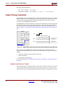
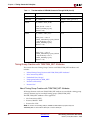
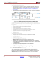
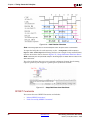
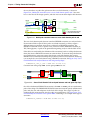
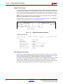
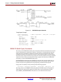
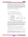
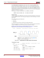
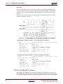
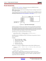
A timing diagram for an ideal System Synchronous SDR interface is shown in Figure 2-2,
“Timing diagram for an ideal System Synchronous SDR interface.” The interface has a
clock period of 5 ns, The data for both bits of the bus remains valid for the entire period.
Tran smit
Edg e
C apture
Ed ge
PERIOD = 5 ns
SysCLk
OFFSET IN BEFORE = 5 ns
Data 1
Da ta
Data 2
Da ta
VALID = 5 ns
Figure 2-2:
Timing diagram for an ideal System Synchronous SDR interface
The global OFFSET IN constraint is:
OFFSET = IN value VALID value BEFORE clock;
In the OFFSET IN constraint, the OFFSET=IN <value> determines the time from the
capturing clock edge to the time in which data first becomes valid. In this system
synchronous example, the data becomes valid 5 ns prior to the capturing clock edge. In the
OFFSET IN constraint, the VALID <value> determines the duration in which data
remains valid. In this example, the data remains valid for 5 ns.
For this example, the complete OFFSET IN specification with associated PERIOD
constraint is:
NET "SysCLk" TNM_NET = "SysClk";
TIMESPEC "TS_SysClk" = PERIOD "SysClk" 5 ns HIGH 50%;
OFFSET = IN 5 ns VALID 5 ns BEFORE "SysClk";
This global constraint covers both the data bits of the bus:
•
data1
•
data2
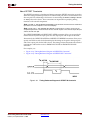
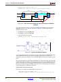
Source Synchronous Inputs
In a source synchronous input interface, a clock is regenerated and transmitted along with
the data from the source device along similar board traces. This clock is then used to
capture the data in the FPGA device. The board trace delays and board skew no longer
limit the operating frequency of the interface. The higher frequency also results in the
source synchronous input interface typically being a dual data rate (DDR) application. In
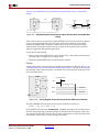
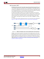
this source synchronous DDR application example, shown in Figure 2-3, “Simplified
Source Synchronous input interface with associated DDR timing,” unique data is
12
www.xilinx.com
Xlinx Timing Constraints User Guide
UG612 (v1.0.0) December 5, 2008
R
Input Timing Constraints
transmitted from the source device on both the rising and falling clock edges and captured
in the FPGA device using the regenerated clock.
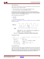
Sour ce D e vice
FP GA
D ata
D
Q
D
Clock
Q
REG
REG
CL K
CLK
Data 1
Rising Data
Falling Data
Data 2
Rising Data
Falling Data
C loc k
D
Q
REG
CL K
Figure 2-3:
Simplified Source Synchronous input interface with associated DDR
timing
The global OFFSET IN constraint is the most efficient way to specify the input timing for a
source synchronous interface. In the DDR interface, one OFFSET IN constraint is defined
for each edge of the input interface clock. These constraints cover the paths of all input data
bits that are captured in registers triggered by the specified input clock edge.
To specify the input timing:
•
Define the clock PERIOD constraint for the input clock associated with the interface
•
Define the global OFFSET IN constraint for the rising edge (RISING) of the interface
•
Define the global OFFSET IN constraint for the falling edge (FALLING) of the
interface
Example
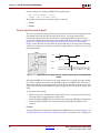
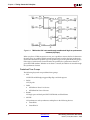
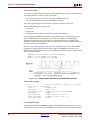
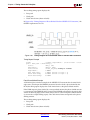
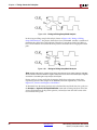
A timing diagram for an ideal Source Synchronous DDR interface is shown in Figure 2-4,
“Timing diagram for ideal Source Synchronous DDR.” The interface has a clock period of
5 ns with a 50/50 duty cycle. The data for both bits of the bus remains valid for the entire
½ period.
PERIOD = 5 n s
SysC Lk
OFFSET IN
1.25 ns
D ata 1
D ata 2
Figure 2-4:
OFFSET IN
1.25 ns
D ata
Da ta
D ata
Da ta
VALID = 2 .5 ns
VAL ID = 2 .5 ns
Timing diagram for ideal Source Synchronous DDR
The global OFFSET IN constraint for the DDR case is:
OFFSET = IN value VALID value BEFORE clock RISING;
OFFSET = IN value VALID value BEFORE clock FALLING;
In the OFFSET IN constraint, OFFSET=IN <value> determines the time from the
capturing clock edge in which data first becomes valid. In this source synchronous input
example, the rising data becomes valid 1.25 ns prior to the rising clock edge. The falling
data also becomes valid 1.25 ns prior to the falling clock edge. In the OFFSET IN constraint,
Xlinx Timing Constraints User Guide
UG612 (v1.0.0) December 5, 2008
www.xilinx.com
13
R
Chapter 2: Timing Constraint Methodology
the VALID <value> determines the duration in which data remains valid. In this
example, both the rising and falling data remains valid for 2.5 ns.
For this example, the complete OFFSET IN specification with associated PERIOD
constraint is:
NET "SysCLk" TNM_NET = "SysClk";
TIMESPEC "TS_SysClk" = PERIOD "SysClk" 5 ns HIGH 50%;
OFFSET = IN 1.25 ns VALID 2.5 ns BEFORE "SysClk" RISING;
OFFSET = IN 1.25 ns VALID 2.5 ns BEFORE "SysClk" FALLING;
This global constraint covers both the data bits of the bus:
•
data1
•
data2
Register-To-Register Timing Constraints
This section discusses Register-To-Register Timing Constraints and includes:
•
“About Input Timing Constraints”
•
“Automatically Related Synchronous DCM/PLL Clock Domains”
•
“Manually Related Synchronous Clock Domains”
•
“Asynchronous Clock Domains”
About Register-To-Register Timing Constraints
Register-to-register or synchronous element to synchronous element path constraints cover the
synchronous data paths between internal registers. The PERIOD constraint:
•
Defines the timing requirements of the clock domains
•
Analyzes the paths within a single clock domain
•
Analyzes all paths between related clock domains
•
Takes into account all frequency, phase, and uncertainty differences between the clock
domains during analysis
For more information, see “PERIOD Constraints” in Chapter 3, “Timing Constraint
Principles.”
The application and methodology for constraining synchronous clock domains falls under
several common cases. These categories include:
•
“Automatically Related Synchronous DCM/PLL Clock Domains”
•
“Manually Related Synchronous Clock Domains”
•
“Asynchronous Clock Domains”
By allowing the tools to automatically create clock relationships for DLL/DCM/PLL
output clocks, and manually defining relationships for externally related clocks, all
synchronous cross clock domain paths are covered by the appropriate constraints, and
properly analyzed. Using PERIOD constraints that follow this methodology eliminates the
need for additional cross-clock-domain constraints.
14
www.xilinx.com
Xlinx Timing Constraints User Guide
UG612 (v1.0.0) December 5, 2008
R
Register-To-Register Timing Constraints
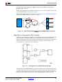
Automatically Related Synchronous DCM/PLL Clock Domains
The most common type of clock circuit is one in which:
•
The input clock is fed into a DLL/DCM/PLL
•
The outputs are used to clock the synchronous paths in the device
In this case, the recommended methodology is to define a PERIOD constraint on the input
clock to the DLL/DCM/PLL.
By placing the PERIOD constraint on the input clock, the Xilinx tools automatically:
•
Derive a new PERIOD constraint for each of the DLL/DCM/PLL output clocks
•
Determine the clock relationships between the output clock domains, and
automatically perform an analysis for any paths between these clock domains.
Example
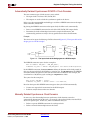
The circuit of an input clock driving a DCM is shown inFigure 2-5, “The input clock of the
design goes to a DCM example.”
Transmi t Edge
R ela ted Pa th
D
Q
D
REG
RE G
CLK
CLK
C LK1X
C LKIN
DCM
PERIOD = 5 ns
Q
CL K1X
CL K2X
C LK2X
Capture Edge
Figure 2-5:
The input clock of the design goes to a DCM example
The PERIOD constraint syntax for this example is:
NET "ClockName" TNM_NET = "TNM_NET_Name";
TIMESPEC "TS_name" = PERIOD "TNM_NET_Name" PeriodValue HIGH HighValue%;
In the PERIOD constraint, the PeriodValue defines the duration of the clock period. In
this case, the input clock to the DCM has a period of 5 ns. The HighValue of the PERIOD
constraint defines the percent of the clock waveform that is HIGH. In this example, the
waveform has a 50/50 duty cycle resulting in a HighValue of 50%.
The syntax for this example is:
NET "ClkIn" TNM_NET = "ClkIn";
TIMESPEC "TS_ClkIn" = PERIOD "ClkIn" 5 ns HIGH 50%;
Based on the input clock PERIOD constraint given above, the DCM automatically:
•
Creates two output clock constraints for the DCM outputs
•
Performs analysis between the two domains
Manually Related Synchronous Clock Domains
In some cases the relationship between synchronous clock domains can not be
automatically determined by the tools - for example, when related clocks enter the FPGA
device on separate pins. In this case, Xilinx recommends that you:
•
Define a separate PERIOD constraint for each input clock
•
Define a manual relationship between the clocks
Xlinx Timing Constraints User Guide
UG612 (v1.0.0) December 5, 2008
www.xilinx.com
15
R
Chapter 2: Timing Constraint Methodology
Once you define the manual relationship, all paths between the two synchronous domains
are automatically analyzed. The analysis takes into account all frequency, phase, and
uncertainty information.
The Xilinx constraints system allows you to define complex manual relationships between
clock domains using the PERIOD constraint including clock frequency and phase
transformations.
To define complex manual relationships between clock domains using the PERIOD
constraint:
•
Define the PERIOD constraint for the primary clock
•
Define the PERIOD constraint for the related clock using the first PERIOD constraint
as a reference
For more information on using the PERIOD constraint to define clock relationships, see
“PERIOD Constraints” in Chapter 3, “Timing Constraint Principles.”
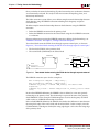
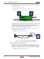
Two related clocks enter the FPGA device through separate external pins, as shown in
Figure 2-6, “Two related clocks entering the FPGA device through separate external pins.”
•
The first clock (CLK1X) is the primary clock
•
The second clock (CLK2X180) is the related clock
Tr ansmit Ed ge
Related Path
D
Q
D
PE RIOD = 5 n s
Q
REG
REG
CL K
CLK
CLK1X
CLK1X
CLK2X180
CLK2X180
Ca pture Edge
Figure 2-6:
Two related clocks entering the FPGA device through separate external
pins
The PERIOD constraint syntax for this example is:
NET "PrimaryClock" TNM_NET = "TNM_Primary";
NET "RelatedClock" TNM_NET = "TNM_Related";
TIMESPEC "TS_primary" = PERIOD "TNM_Primary" PeriodValue HIGH
HighValue%;
TIMESPEC "TS_related" = PERIOD "TNM_Related" TS_Primary_relation PHASE
value;
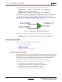
In the related PERIOD definition, the PERIOD value is defined as a time unit (period)
relationship to the primary clock. The relationship is expressed in terms of the primary
clock TIMESPEC. In this example CLK2X180 operates at twice the frequency of CLK1X
which results in a PERIOD relationship of one-half.
In the related PERIOD definition, the PHASE value defines the difference in time between
the rising clock edge of the source clock and the related clock. In this example, since the
CLK2X180 clock is 180 degrees shifted, the rising edge begins 1.25 ns after the rising edge
of the primary clock.
16
www.xilinx.com
Xlinx Timing Constraints User Guide
UG612 (v1.0.0) December 5, 2008
R
Register-To-Register Timing Constraints
The syntax for this example is:
NET "Clk1X" TNM_NET = "Clk1X";
NET "Clk2X180" TNM_NET = "Clk2X180";
TIMESPEC "TS_Clk1X" = PERIOD "Clk1X" 5 ns;
TIMESPEC "TS_Clk2X180" = PERIOD "Clk2X180" TS_Clk1X/2 PHASE + 1.25 ns ;
Asynchronous Clock Domains
Asynchronous clock domains are those in which the source and destination clocks do not
have a frequency or phase relationship. Since the clocks are not related, it is not possible to
determine the final relationship for setup and hold time analysis. For this reason, Xilinx
recommends that you use proper asynchronous design techniques to ensure the successful
capture of data. One example of proper asynchronous design technique is to use a FIFO
design element to capture and transfer data between asynchronous clock domains. While
not required, in some cases you may wish to constrain the maximum data path delay in
isolation without regard to clock path frequency or phase relationship.
The Xilinx constraints system allows you to constrain the maximum data path delay
without regard to source and destination clock frequency and phase relationship. This
requirement is specified using the FROM-TO constraint with the DATAPATHONLY
keyword.
To constrain of the maximum data path delay without regard to source and destination
clock frequency and phase relationship:
•
Define a time group for the source synchronous elements
•
Define a time group for the destination synchronous elements
•
Define the maximum delay of the data paths using the FROM-TO constraint between
the two time groups with DATAPATHONLY keyword.
For more information on using the FROM-TO constraint with the DATAPATHONLY
keyword, see “FROM:TO (Multi-Cycle) Constraints” in Chapter 3, “Timing Constraint
Principles.”
Example
Two unrelated clocks enter the FPGA device through separate external pins as shown in
Figure 2-7, “Two unrelated clocks entering the FPGA device through separate external
pins.”
•
The first clock (CLKA) is the source clock
•
The second clock (CLKB) is the destination clock
Data_A_B
D
Q
D
Q
REG
R EG
CLK
CLK
CLKA
CLKB
Figure 2-7:
Xlinx Timing Constraints User Guide
UG612 (v1.0.0) December 5, 2008
Two unrelated clocks entering the FPGA device through separate
external pins
www.xilinx.com
17
R
Chapter 2: Timing Constraint Methodology
The syntax for this example is:
NET "CLKA" TNM_NET = FFS "GRP_A";
NET "CLKB" TNM_NET = FFS "GRP_B";
TIMESPEC TS_Example = FROM "GRP_A" TO "GRP_B" 5 ns DATAPATHONLY;
Output Timing Constraints
Output timing covers the data path from a register inside the FPGA device to the external
pin of the FPGA device. The OFFSET OUT constraint specifies the output timing. The best
way to specify the output timing requirements depends on the type (source/system
syncronous) and SDR/DDR of the interface.
The OFFSET OUT constraint defines the maximum time allowed for data to be transmitted
from the FPGA device. The output delay path begins at the input clock pin of the FPGA
device and continues through the output register to the data pins of the FPGA device, as
shown in Figure 2-8, “Output-timing constraints from input clock pad to the output data
pad.”
F PGA
Data1
D
ClkIn
Q
REG
OFFSET OUT AFTER
CLK
Data2
D
D ata1
Valid D ata
D ata2
Valid D ata
Q
REG
CLK
C lkIn
Figure 2-8:
Output-timing constraints from input clock pad to the output data pad
When analyzing the OFFSET OUT constraint, the timing tools automatically take all
internal factors affecting the delay of the clock and data paths into account. These factors
include:
•
Frequency and phase transformations of the clock
•
Clock uncertainties
•
Data path delay adjustments
For more information, see “OFFSET OUT Constraints” in Chapter 3, “Timing Constraint
Principles.”
System Synchronous Output
The system synchronous output interface is an interface in which a common system clock
is used to both transfer and capture the data. Since this interface uses a common system
clock, only the data is transmitted from the FPGA device to the receiving device as shown
18
www.xilinx.com
Xlinx Timing Constraints User Guide
UG612 (v1.0.0) December 5, 2008
R
Output Timing Constraints
in Figure 2-9, “Simplified System Synchronous output interface with associated SDR
timing.”
FPGA
Receiving Device
Data
D
Q
D
Transmit
Edge
Q
REG
REG
CLK
CL K
Capture
Edge
System Clock
Data
Data
System Clock
Figure 2-9:
Simplified System Synchronous output interface with associated SDR
timing
If these paths must be constrained, the global OFFSET OUT constraint is the most efficient
way to specify the output timing for the system synchronous interface. In the global
method, one OFFSET OUT constraint is defined for each system synchronous output
interface clock. This single constraint covers the paths of all output data bits sent from
registers triggered by the specified input clock.
To specify the output timing:
•
Define a time name (TNM) for the output clock to create a time group, which contains
all output registers triggered, by the input clock
•
Define the global OFFSET OUT constraint for the interface
Example
A timing diagram for a System Synchronous SDR output interface is shown in Figure 2-10,
“Timing diagram for System Synchronous SDR output interface.” The data in this example
must become valid at the output pins a maximum of 5 ns after the input clock edge at the
pin of the FPGA device.
FPGA
Input Clock Edge
D ata 1
D
Q
ClkIn
REG
CLK
OF F SET OU T AFT ER
5 ns
D ata 2
D
Q
Data1
Valid Data
Data2
Valid Data
REG
CLK
C lkIn
Figure 2-10:
Timing diagram for System Synchronous SDR output interface
The global OFFSET OUT constraint for the system synchronous interface is:
OFFSET = OUT value AFTER clock;
In the OFFSET OUT constraint, OFFSET=OUT <value> determines the maximum time
from the rising clock edge at the input clock port until the data first becomes valid at the
data output port of the FPGA device. In this system synchronous example, the output data
must become valid at least 5 ns after the input clock edge.
Xlinx Timing Constraints User Guide
UG612 (v1.0.0) December 5, 2008
www.xilinx.com
19
R
Chapter 2: Timing Constraint Methodology
For this example, the complete OFFSET OUT specification is:
NET "ClkIn" TNM_NET = "ClkIn";
OFFSET = OUT 5 ns AFTER "ClkIn";
This global constraint covers both the data bits of the bus:
•
data1
•
data2
Source Synchronous Outputs
The source synchronous output interface is an interface in which a clock is regenerated and
transmitted along with the data from the FPGA device. The regenerated clock is
transmitted along with the data. The interface is primarily limited in performance by
system noise and the skew between the regenerated clock and the data bits, as shown in
Figure 2-11, “Simplified Source Synchronous output interface with associated DDR
timing.” In this interface, the time from the input clock edge to the output data becoming
valid is not as important as the skew between the output data bits. In most cases, it can be
left unconstrained.
FPGA
ClkIn
Data1
D
Q
REG
CL K
ClkOut
V CC
ClkOut
D
GND
Q
REG
CL K
Data1
Rising Data
Falling Data
ClkIn
Figure 2-11: Simplified Source Synchronous output interface with associated DDR
timing
The global OFFSET OUT constraint is the most efficient way to specify the output timing
for a source synchronous interface. In the DDR interface, one OFFSET OUT constraint is
defined for each edge of the output interface clock. These constraints cover the paths of all
output data bits that are transmitted by registers triggered with the specified output clock
edge.
To specify the input timing:
•
Define a time name (TNM) for the output clock to create a time group which contains
all output registers triggered by the output clock
•
Define the global OFFSET OUT constraint for the rising edge (RISING) of the interface
•
Define the global OFFSET OUT constraint for the falling edge (FALLING) of the
interface
Example
A timing diagram for an ideal Source Synchronous DDR interface is shown in Figure 2-12,
“Timing diagram for an ideal Source Synchronous DDR.” The interface has a clock period
20
www.xilinx.com
Xlinx Timing Constraints User Guide
UG612 (v1.0.0) December 5, 2008
R
Timing Exceptions
of 5 ns with a 50/50 duty cycle. The data for both bits of the bus remains valid for the entire
½ period.
PER IOD = 5 ns
SysC Lk
OFFSET IN
1.25 ns
OFFSET IN
1.25 ns
D ata 1
D ata
D ata
D ata 2
D ata
D ata
VAL ID = 2 .5 ns
VALID = 2.5 n s
Figure 2-12:
Timing diagram for an ideal Source Synchronous DDR
The global OFFSET IN constraint for the DDR case is:
OFFSET = IN value VALID value BEFORE clock RISING;
OFFSET = IN value VALID value BEFORE clock FALLING;
In the OFFSET IN constraint, OFFSET=IN <value> determines the time from the
capturing clock edge in which data first becomes valid. In this source synchronous input
example, the rising data becomes valid 1.25 ns prior to the rising clock edge and the falling
data also becomes valid 1.25 ns prior to the falling clock edge. In the OFFSET IN constraint,
VALID <value> determines the duration in which data remains valid. In this example,
both the rising and falling data remains valid for 2.5 ns.
For this example, the complete OFFSET IN specification with associated PERIOD
constraint is:
NET "SysCLk" TNM_NET = "SysClk";
TIMESPEC "TS_SysClk" = PERIOD "SysClk" 5 ns HIGH 50%;
OFFSET = IN 1.25 ns VALID 2.5 ns BEFORE "SysClk" RISING;
OFFSET = IN 1.25 ns VALID 2.5 ns BEFORE "SysClk" FALLING;
In the OFFSET OUT constraint, OFFSET=OUT <value> determines the maximum time
from the rising clock edge at the input clock port until the data first becomes valid at the
data output port of the FPGA device. When <value> is omitted from the OFFSET OUT
constraint, the constraint becomes a report-only specification which reports the skew of the
output bus. The REFERENCE_PIN keyword defines the regenerated output clock as the
reference point against which the skew of the output data pins is reported.
For this example, the complete OFFSET OUT specification for both the rising and falling
clock edges is :
NET “CLkIn” TNM_NET = “ClkIn”;
OFFSET = OUT AFTER “ClkIn” REFERENCE_PIN “ClkOut” RISING;
OFFSET = OUT AFTER “ClkIn” REFERENCE_PIN “ClkOut” FALLING;
Timing Exceptions
Using the global definitions of the input, register-to-register, and output timing
constraints, properly constrains the majority of the paths. In certain cases a small number
of paths contain exceptions to the global constraint rules. The most common types of
exceptions are:
•
“False Paths”
•
“Multi-Cycle Paths”
Xlinx Timing Constraints User Guide
UG612 (v1.0.0) December 5, 2008
www.xilinx.com
21
R
Chapter 2: Timing Constraint Methodology
False Paths
In some cases, you may want to remove a set of paths from timing analysis if you are sure
that these paths do not affect timing performance.
One common way to specify the set of paths to be removed from timing analysis is to use
the FROM-TO constraint with the timing ignore (TIG) keyword. This allows you to:
•
Specify a set of registers in a source time group
•
Specify a set of registers in a destination time group
•
Automatically remove all paths between those time groups from analysis.
To specify the timing ignore (TIG) constraint for this method, define:
•
A set of registers for the source time group
•
A set of registers for the destination time group
•
A FROM-TO constraint with a TIG keyword to remove the paths between the groups
Example
A hypothetical case in which a path between two registers does not affect the timing of the
design, and is desired to be removed from analysis, is shown in Figure 2-13,“Path between
two registers that does not affect the timing of the design.”
Ignored Path
D
Q
D
Q
REG
REG
CLK
CLK
CLK1
CLK2
Figure 2-13:
Path between two registers that does not affect the timing of the
design
The generic syntax for defining a timing ignore (TIG) between time groups is:
TIMESPEC "TSid" = FROM "SRC_GRP" TO "DST_GRP" TIG;
In the FROM-TO TIG example, the SRC_GRP defines the set of source registers at which
path tracing begins. The DST_GRP defines the set of destination registers at which the path
tracing ends. All paths that begin in the SRC_GRP and end in the DST_GRP are ignored.
The specific syntax for this example is:
NET "CLK1" TNM_NET = FFS "GRP_1";
NET "CLK2" TNM_NET = FFS "GRP_2";
TIMESPEC TS_Example = FROM "GRP_1" TO "GRP_2" TIG;
Multi-Cycle Paths
In a multi-cycle path, data is transferred from source to destination synchronous elements
at a rate less than the clock frequency defined in the PERIOD specification.
This occurs most often when the synchronous elements are gated with a common clock
enable signal. By defining a multi-cycle path, the timing constraints for these synchronous
22
www.xilinx.com
Xlinx Timing Constraints User Guide
UG612 (v1.0.0) December 5, 2008
R
Timing Exceptions
elements are relaxed over the default PERIOD constraint. The implementation tools are
then able to appropriately prioritize the implementation of these paths.
One common way to specify the set of multi-cycle paths is to define a time group using the
clock enable signal. This allows you to:
•
Define one time group containing both the source and destination synchronous
elements using a common clock enable signal
•
Automatically apply the multi-cycle constraint to all paths between these
synchronous elements
To specify the FROM:TO (multi-cycle) constraint for this method, define:
•
A PERIOD constraint for the common clock domain
•
A set of registers based on a common clock enable signal
•
A FROM:TO (multi-cycle) constraint describing the new timing requirement
Example
Figure 2-14, “Path between two registers clocked by a common clock enable signal,” shows
a hypothetical case in which a path between two registers is clocked by a common clock
enable signal. In this example, the clock enable is toggled at a rate that is one-half of the
reference clock.
Multi-Cycle Path
D
Q
REG
CLK
EN
D
Q
REG
CLK
EN
D
Q
REG
CLK
EN
D
Q
R EG
CLK
EN
CLK1
Enable
Figure 2-14:
Path between two registers clocked by a common clock enable signal
The generic syntax for defining a multi-cycle path between time groups is:
TIMESPEC "TSid" = FROM "MC_GRP" TO "MC_GRP" <value>;
In the FROM:TO (multi-cycle) example, the MC_GRP defines the set of registers which are
driven by a common clock enable signal. All paths that begin in the MC_GRP and end in
the MC_GRP have the multi-cycle timing requirement applied to them. Paths into and out
of the MC_GRP are analyzed with the appropriate PERIOD specification.
The specific syntax for this example is:
NET "CLK1" TNM_NET = "CLK1";
TIMESPEC "TS_CLK1" = PERIOD "CLK1" 5 ns HIGH 50%;
NET "Enable" TNM_NET = FFS "MC_GRP";
TIMESPEC TS_Example = FROM "MC_GRP" TO "MC_GRP" TS_CLK1*2;
Xlinx Timing Constraints User Guide
UG612 (v1.0.0) December 5, 2008
www.xilinx.com
23
R
Chapter 2: Timing Constraint Methodology
24
www.xilinx.com
Xlinx Timing Constraints User Guide
UG612 (v1.0.0) December 5, 2008
R
Chapter 3
Timing Constraint Principles
This chapter includes:
•
“Constraint System”
•
“Constraint Priorities”
•
“Timing Constraints”
•
“Timing Constraint Syntax”
•
“Creating Timing Constraints”
•
“Timing Constraint Analysis”
•
“Clock Skew”
•
“Clock Uncertainty”
•
“Asynchronous Reset Paths”
This chapter:
•
Discusses the fundamentals of timing constraints, including:
♦
“PERIOD Constraints”
♦
“OFFSET Constraints”
♦
“FROM:TO (Multi-Cycle) Constraints”
•
Discusses the ability to group elements in order to provide a better understanding of
the constraint system subsystem
•
Provides more information about the analysis of the basic constraints, with “Clock
Skew” and “Clock Uncertainty”
Constraint System
This section discusses the Constraint System and includes:
•
“About the Constraint System”
•
“DLL/DCM/PLL/BUFR/PMCD Components”
•
“Timing Group Creation with TNM/TNM_NET Attributes”
•
“Grouping Constraints”
About the Constraint System
The constraint system is that portion of the implementation tools (NGDBUILD) that parses
and understands the physical and timing constraints for the design.
Xlinx Timing Contstraints User Guide
UG612 (v1.0.0) December 5, 2008
www.xilinx.com
25
R
Chapter 3: Timing Constraint Principles
The constraint system:
•
Parses the constraints from the following files and delivers this information to the
other implementation tools:
♦
NCF
♦
UCF
♦
EDN/EDF/EDIF
♦
NGC
♦
NGO
•
Confirms that the constraints are correctly specified for the design
•
Applies the necessary attributes to the corresponding elements
•
Issues error and warning messages for constraints that do not correlate correctly with
the design
DLL/DCM/PLL/BUFR/PMCD Components
This section discusses DLL/DCM/PLL/BUFR/PMCD Components and includes:
•
“About DLL/DCM/PLL/BUFR/PMCD Components”
•
“Transformation Conditions”
•
“New PERIOD Constraints on DCM Outputs”
•
“The newly created TIMESPEC PERIOD constraints contain all the paths associated
with the clock modifying block component. If the PERIOD constraint is not translated
and then traces only to the clock modifying block component, the timing report show
0 items analyzed. No other PERIOD constraints are reported.”
•
“Analysis with NET PERIOD”
•
“PHASE Keyword”
•
“DLL/DCM/PLL Manipulation with PHASE”
About DLL/DCM/PLL/BUFR/PMCD Components
When a TIMESPEC PERIOD specification on the input pad clock net is traced or translated
through the DCM/DLL/PLL/BUFR/PMCD component (also known as a clockmodifying block), the derived or output clocks are constrained with new PERIOD
constraints.
In order to generate the destination-element-timing group, during transformation each
clock output pin of the clock-modifying block is given:
•
A new TIMESPEC PERIOD constraint
•
A corresponding TNM_NET constraint
The new TIMESPEC PERIOD constraint is based upon the manipulation of the clock
modifying block component. The transformation:
26
•
Takes into account the phase relationship factor of the clock outputs
•
Performs the appropriate multiplication or division of the PERIOD requirement value
www.xilinx.com
Xlinx Timing Contstraints User Guide
UG612 (v1.0.0) December 5, 2008
R
Constraint System
Transformation Conditions
The transformation occurs when:
•
The TIMESPEC PERIOD constraint is traced into the CLKIN pin of the clock
modifying block component, and
•
The following conditions are met:
♦
The group associated with the PERIOD constraint is used in exactly one PERIOD
constraint
♦
The group associated with the PERIOD constraint is not used in any other timing
constraints, including FROM:TO (multicycle) or OFFSET constraints
♦
The group associated with the PERIOD constraint is not referenced or related to
any other user group definition
New PERIOD Constraints on DCM Outputs
If the “Transformation Conditions” are met, the TIMESPEC "TS_clk20" = PERIOD
"clk20_grp" 20 ns HIGH 50 %; constraint is translated into the following constraints
based upon the clock structure shown in Figure 3-1, “New PERIOD Constraints on DCM
Outputs.”
CLK0:
TS_clk20_0=PERIOD clk20_0 TS_clk20*1.000000 HIGH 50.000000%
CLK90: TS_clk20_90=PERIOD clk20_90 TS_clk20*1.000000 PHASE + 5.000000
nS HIGH 50.000000%
Figure 3-1: New PERIOD Constraints on DCM Outputs
The following message appears in the NGDBuild (design.bld) or MAP (design.mrp)
report:
INFO:XdmHelpers:851 - TNM " clk20_grp ", used in period specification
"TS_clk20", was traced into DCM instance "my_dcm". The following new TNM
groups and period specifications were generated at the DCM output(s):
clk0: TS_clk20_0=PERIOD clk20_0 TS_clk20*1.000000 HIGH 50.000000%
clk90: TS_clk20_90=PERIOD clk20_90 TS_clk20*1.000000 PHASE + 5.000000
nS HIGH 50.000000%
If the CLKIN_DIVIDE_BY_2 attribute is set to TRUE for the DCM in Figure 3-1, “New
PERIOD Constraints on DCM Outputs,” the translated PERIOD constraints are adjusted
accordingly. The following constraints are the result of this attribute:
CLK0:
TS_clk20_0=PERIOD clk20_0 TS_clk20*2.000000 HIGH 50.000000%
CLK90: TS_clk20_90=PERIOD clk20_90 TS_clk20*2.000000 PHASE + 5.000000
nS HIGH 50.000000%
Xlinx Timing Contstraints User Guide
UG612 (v1.0.0) December 5, 2008
www.xilinx.com
27
R
Chapter 3: Timing Constraint Principles
If the “Transformation Conditions” are not met:
•
The PERIOD constraint is not placed on the output or derived clocks of the clock
modifying block component, and
•
An error or warning message is reported in the NGDBuild report
Error Message Example
Following is an example of an error message:
"ERROR:NgdHelpers:702 - The TNM "PAD_CLK" drives the CLKIN pin of CLKDLL
"$I1". This TNM cannot be traced through the CLKDLL because it is not
used in exactly one PERIOD specification. This TNM is used in the
following user groups and/or specifications:
TS_PAD_CLK=PERIOD PAD_CLK 20000.000000 pS HIGH 50.000000%
TS_01=FROM PAD_CLK TO PADS 20000.000000 pS"
Note: The original TIMESPEC PERIOD constraint is reported in the timing report and shows "0
items analyzed."
The newly created TIMESPEC PERIOD constraints contain all the paths associated with
the clock modifying block component. If the PERIOD constraint is not translated and then
traces only to the clock modifying block component, the timing report show 0 items
analyzed. No other PERIOD constraints are reported.
If the PERIOD constraint traces to other synchronous elements, the analysis includes only
those synchronous elements.
Synchronous Elements
Synchronous elements include:
28
•
Flip Flops
•
Latches
•
Distributed RAM
•
Block RAM
•
Distributed ROM
•
ISERDES
•
OSERDES
•
PPC405
•
PPC440
•
MULT18X18
•
DSP48
•
MGTs (GT, GT10, GT11, GTP)
•
SRL16
•
EMAC
•
FIFO (16, 18, & 36)
•
PCIE
•
TEMAC
www.xilinx.com
Xlinx Timing Contstraints User Guide
UG612 (v1.0.0) December 5, 2008
R
Constraint System
Analysis with NET PERIOD
When a NET PERIOD constraint is applied to the input clock pad or net, this constraint is
not translated through the clock modifying block component. This can result in zero items
or paths analyzed for these constraints.
The NET PERIOD is analyzed only during MAP, PAR, and Timing analysis. When "MAP timing" and PAR call the timing tools, the timing tools do the clock modifying block
manipulation for placement and routing, but not for the timing analysis timing reports.
When a TIMESPEC PERIOD constraint is traced into an input pin on a clock modifying
block, NGDBuild or the translate process transforms the original TIMESPEC PERIOD
constraint into new TIMESPEC PERIOD constraints based upon the derived output clocks.
The NGDBuild report (design.bld) indicates this transformation.
MAP, PAR, and Timing Analyzer use the new derived clock TIMESPEC PERIOD
constraints that are propagated to the Physical Constraints File (PCF). The original
TIMESPEC PERIOD is unchanged during this transformation. It is used as a reference for
the new TIMESPEC PERIOD constraints.
Note: Constraints Editor sees only the original PERIOD constraint and not the newly transformed
PERIOD constraints.
PHASE Keyword
The PHASE keyword is used in the relationship between related clocks. The timing
analysis tools use this relationship for the OFFSET constraints and cross-clock domain path
analysis. The PHASE keyword can be entered in the UCF/NCF or through the translation
of the DCM/DLL/PLL components during NGDBuild.
Note: If the phase shifted value of DCM/PLL/DLL component is changed in FPGA Editor, the
change is not reflected in the PCF file.
The timing analysis tools use the PHASE keyword value in the PCF to emulate the
DLL/DCM/PLL phase shift value. In order to see the change that was made in FPGA
Editor, the PCF must also be modified manually with the corresponding change.
DLL/DCM/PLL Manipulation with PHASE
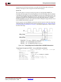
Table 3-1, “Transformation of PERIOD Constraint Through DCM,” displays the new
DCM/DLL/PLL component output clock net derived TIMESPEC PERIOD constraints,
based upon the original PERIOD (TS_CLKIN) constraints. TS_CLKIN is expressed as a
time value.
If TS_CLKIN is expressed as a frequency value, the multiply and divide operations are
reversed. If the DCM attributes FIXED_PHASE_SHIFT or VARIABLE_PHASE_SHIFT are
used, the amount of the phase-shifted value is included in the PHASE keyword value.
The DCM attributes FIXED_PHASE_SHIFT or VARIABLE_PHASE_SHIFT phase shifting
amount on the DCM is not reflected in Table 3-1, “Transformation of PERIOD Constraint
Through DCM.”
Table 3-1:
Transformation of PERIOD Constraint Through DCM
Output Pin
PERIOD Value
PHASE Shift value
CLK0
TS_CLKIN * 1
None
CLK90
TS_CLKIN * 1
PHASE + (clk0_period * ¼)
CLK180
TS_CLKIN * 1
PHASE + (clk0_period * ½)
Xlinx Timing Contstraints User Guide
UG612 (v1.0.0) December 5, 2008
www.xilinx.com
29
R
Chapter 3: Timing Constraint Principles
Table 3-1:
Transformation of PERIOD Constraint Through DCM (Cont’d)
CLK270
TS_CLKIN * 1
PHASE + (clk0_period * ¾)
CLK2x
TS_CLKIN / 2
None
CLK2x180
TS_CLKIN / 2
PHASE + (clk2x_period * ½)
CLKDV
TS_CLKIN * clkdv_divide
None
(clkdv_divide = value of
CLKDV_DIVIDE property
(default = 2.0))
CLKFX
TS_CLKIN / clkfx_factor
None
(clkfx_factor = value of
CLKFX_MULTIPLY property (default
= 4.0) divided by value of
CLKFX_DIVIDE property
(default = 1.0))
CLKFX180
TS_CLKIN / clkfx_factor
PHASE + (clkfx_period * ½)
(clkfx_factor = value of
CLKFX_MULTIPLY property (default
= 4.0) divided by value of
CLKFX_DIVIDE property
(default = 1.0))
Timing Group Creation with TNM/TNM_NET Attributes
This section discusses Timing Group Creation with TNM/TNM_NET Attributes and
includes:
•
“About Timing Group Creation with TNM/TNM_NET Attributes”
•
“Net Connectivity (NET)”
•
“Predefined Time Groups”
•
“Propagation Rules for TNM_NET”
•
“Instance or Hierarchy”
•
“Instance Pin”
About Timing Group Creation with TNM/TNM_NET Attributes
All design elements with same TNM/TNM_NET attribute are considered a timing group.
A design element may be in multiple timing groups (TNM/TNM_NET).
The NM/TNM_NET attributes can be applied to:
•
Net Connectivity (NET)
•
Instance/Module - INST
•
Instance Pin - PIN
Note: To ensure correct timing analysis, Xilinx® recommends that you place only one
TNM/TNM_NET on each element, driver pin, or macro driver pin.
30
www.xilinx.com
Xlinx Timing Contstraints User Guide
UG612 (v1.0.0) December 5, 2008
R
Constraint System
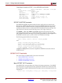
Net Connectivity (NET)
Identifying groups by net connectivity allows the grouping of elements by specifying a net
or signal that eventually drives synchronous elements and pads. This method is a good
way to identify multi-cycle path elements that are controlled by a clock enable and can be
constrained as a FROM:TO (multi-cycle) constraint. This method uses TNM_NET (timing
net) or TNM (timing name) on a net of the design. The timing name attribute is commonly
used on HDL port declarations, which are directly connected to pads.
If a timing name attribute is placed on a net or signal, the constraints parser traces the
signal or net downstream to the synchronous elements. A timing name is an attribute that
can be used to identify the elements that make up a time group that can be then used in a
timing constraint. Those synchronous elements are then tagged with the same timing
name attribute. The timing name attribute name is then used in a TIMESPEC or Timing
Constraint.
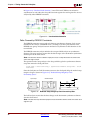
An example is the clock net in following schematic is traced forward to the two flip-flops in
Figure 3-2, “TNM on the CLOCK pad or net traces downstream to the Flip-Flops.”
Figure 3-2:
TNM on the CLOCK pad or net traces downstream to the Flip-Flops
Flagging a common input (typically a clock signal or clock enable signal) can be used to
group flip-flops, latches, or other synchronous elements. The TNM is traced forward along
the path (through any number of gates, buffers, or combinatorial logic) until it reaches a
flip-flop, input latch, or synchronous element. Those elements are added to the specified
TNM or time group. Using TNM on a net that traces forward to create a group of flip-flops
is shown in Figure 3-3, “TNM on the CLK net traced through combinatorial logic to
synchronous elements (flip-flops).”
Xlinx Timing Contstraints User Guide
UG612 (v1.0.0) December 5, 2008
www.xilinx.com
31
R
Chapter 3: Timing Constraint Principles
Figure 3-3:
TNM on the CLK net traced through combinatorial logic to synchronous
elements (flip-flops)
When you place a TNM constraint on a net, use a qualifier to narrow the list of elements in
the time group. A qualified TNM is traced forward until it reaches the first synchronous
element that matches the qualifier type. The qualifier types are the predefined time groups.
If that type of synchronous element matches the qualifier, the synchronous element is
given that TNM attribute. Whether or not there is a match, the TNM is not traced through
the synchronous element.
Predefined Time Groups
The following keywords are predefined time groups:
•
FFS
All SLICE and IOB edge-triggered flip-flops and shift registers
•
PADS
All I/O pads
•
•
DSPS
♦
All DSP48 in Virtex™-4 devices
♦
All DSP48E in Virtex-5 devices
RAMS
All single-port and dual-port SLICE LUT RAMs and block Rams
•
MULTS
All synchronous and asynchronous multipliers in the following devices:
32
♦
VirtexII-Pro
♦
VirtexII-ProX
www.xilinx.com
Xlinx Timing Contstraints User Guide
UG612 (v1.0.0) December 5, 2008
R
Constraint System
•
♦
Virtex-4
♦
Virtex-5
HSIOS
♦
♦
•
-
VirtexII-Pro
-
VirtexII-ProX
-
Virtex-4
All GTP in Virtex-5 devices
CPUS
♦
♦
•
All GT and GT10 in the following devices:
All PPC405 in the following devices:
-
VirtexII-Pro
-
VirtexII-ProX
-
Virtex-4
All PPC450 in Virtex-5 devices
LATCHES
All SLICE level-sensitive latches
•
BRAMS_PORTA
Port A of all dual-port block RAMs
•
BRAMS_PORTB
Port B of all dual-port block RAMs
The TNM_NET is equivalent to TNM on a net, but produces different results on pad nets.
The Translate Process or NGDBuild command never transfers a TNM_NET constraint
from the attached net to an input pad, as it does with the TNM constraint. You can use
TNM_NET only with nets. If TNM_NET is used with any other objects (such as a pin or
instance), a warning is generated and TNM_NET definition is ignored.
A TNM attribute on a pad net or the net between the IPAD and the IBUF, the constraints
parser traces the signal or net upstream to the pad element, as shown in Figure 3-4,
“Differences between TNM and TNM_NET.” The TNM_NET attribute is traced through
the buffer to the synchronous elements. In HDL designs, the IBUF output signal is the
same as the IPAD or port name, so there are not differences between the TNM_NET and
TNM attributes. In this case, both timing name attributes trace downstream to the
synchronous elements.
Propagation Rules for TNM_NET
The propagation rules for TNM_NET are:
•
If applied to a pad net, TNM_NET propagates forward through the IBUF elements
and any other combinatorial logic to synchronous elements or pads.
•
If applied to a clock-pad net, TNM_NET propagates forward through the clock buffer
to synchronous elements or pads.
•
If applied to an input clock net of a DCM/DLL/PLL/PMCD/BUFR and associated
with a PERIOD constraint, TNM_NET propagates forward through the clockmodifying block to synchronous elements or pads.
Xlinx Timing Contstraints User Guide
UG612 (v1.0.0) December 5, 2008
www.xilinx.com
33
R
Chapter 3: Timing Constraint Principles
Figure 3-4:
Differences between TNM and TNM_NET
In the design shown in Figure 3-4, “Differences between TNM and TNM_NET,” a TNM
associated with the IPAD signal includes only the PAD symbol as the member of a time
group. A TNM_NET associated with the IPAD signal includes all the synchronous
elements after the IBUF as members of a time group.
Following are examples of different ways to create time groups using the IPAD signal:
•
NET PADCLK TNM = PAD_grp;
Use the padclk net to define the time group PAD_grp. Contains the IPAD element.
•
NET PADCLK TNM = FFS "FF_grp";
Use the padclk net to define the time group FF_grp. Contains no flip-flop elements.
•
NET PADCLK TNM_NET = FFS FF2_grp;
Use the padclk net to define the time group FF2_grp. Contains all flip-flop elements
associated with this net.
In the design shown in Figure 3-4, “Differences between TNM and TNM_NET,” a TNM
associated with the IBUF output signal can only include the synchronous elements after
the IBUF as members of a time group.
Following are examples of time groups that use only the IBUF output signal:
•
NET INTCLK TNM = FFS FF1_grp;
Use the intclk net to define the time group FF1_grp. Contains all flip-flop elements
associated with this net.
•
NET INTCLK TNM_NET = RAMS Ram1_grp;
Use the intclk net to define the time group Ram1_grp. Contains all distributed and
block RAM elements associated with this net.
Instance or Hierarchy
When a TNM attribute is placed on a module or macro, the constraints parser traces the
macro or module down the hierarchy to the synchronous elements and pads. The attribute
transverses through all levels of the hierarchy rather than forward along a net or signal.
This feature is illustrated in:
34
•
Figure 3-2, “TNM on the CLOCK pad or net traces downstream to the Flip-Flops”
•
Figure 3-3, “TNM on the CLK net traced through combinatorial logic to synchronous
elements (flip-flops)”
www.xilinx.com
Xlinx Timing Contstraints User Guide
UG612 (v1.0.0) December 5, 2008
R
Constraint System
Those synchronous elements are then tagged with the same TNM attribute. The TNM
attribute name is then used in a TIMESPEC or timing constraint. This method uses a TNM
on a block of the design. Multiple instances of the same TNM attribute are used to identify
the time group.
A macro or module is an element that performs some general purpose higher level
function. It typically has a lower level design that consists of primitives or elements, other
macros or modules, or both, connected together to implement the higher level function.
A TNM constraint attached to a module or macro indicates that all elements inside the
macro or module (at all levels of hierarchy below the tagged module or macro) are part of
the named time group. Use the keep_hierarchy attribute to ensure that the design
hierarchy is maintained. This feature is illustrated in:
•
Figure 3-5, “The TNM on the upper left hierarchy is traced down to the lower level
element”
•
Figure 3-6, “Grouping via Instances”
Figure 3-5:
Xlinx Timing Contstraints User Guide
UG612 (v1.0.0) December 5, 2008
The TNM on the upper left hierarchy is traced down to the lower level
element
www.xilinx.com
35
R
Chapter 3: Timing Constraint Principles
Figure 3-6:
Grouping via Instances
You can use wildcard characters to transverse the hierarchy of a design.
•
A question mark (?) represents one character.
•
An asterisk (*) represents multiple characters.
The following example uses a wildcard character to transverse the hierarchy where
Level1 is a top level module:
•
Level1/*
Transverses all blocks in Level1 and below
•
Level1/*/
Transverses all blocks in Level1 but no further
The instances described below are either:
•
Symbols on a schematics, or
•
A symbol name as it appears in the EDIF netlist
An example of the wildcard transversing the design hierarchy is shown in Figure 3-6,
“Grouping via Instances,” for the following instances:
•
INST *
All synchronous elements are in this time group
•
INST /*
All synchronous elements are in this time group
•
INST /*/
Top level elements or modules are in this time group:
36
♦
A1
♦
B1
♦
C1
www.xilinx.com
Xlinx Timing Contstraints User Guide
UG612 (v1.0.0) December 5, 2008
R
Constraint System
•
INST A1/*
All elements one or more levels of hierarchy below the A1 hierarchy are in this time
group:
•
♦
A21
♦
A22
♦
A3
♦
A4
INST A1/*/
All elements one level of hierarchy below the A1 hierarchy are in this time group:
•
♦
A21
♦
A22
INST A1/*/*
All elements two or more levels of hierarchy below the A1 hierarchy are in this time
group:
•
♦
A3
♦
A4
INST A1/*/*/
All elements two levels of hierarchy below the A1 hierarchy are in this time group:
♦
•
A3
INST A1/*/*/*
All elements three or more levels of hierarchy below the A1 hierarchy are in this time
group:
♦
•
A4
INST A1/*/*/*/
All elements three levels of hierarchy below the A1 hierarchy are in this time group:
♦
•
A4
INST /*/*22/
All elements with instance name of 22 are in this time group:
•
♦
A22
♦
B22
♦
C22
INST /*/*22
All elements with instance name of 22 and elements one level of hierarchy below are in
this time group:
♦
A22
♦
A3
♦
A4
♦
B22
♦
B3
Xlinx Timing Contstraints User Guide
UG612 (v1.0.0) December 5, 2008
www.xilinx.com
37
R
Chapter 3: Timing Constraint Principles
♦
C22
♦
C3
Figure 3-7:
Transversing hierarchy with wildcards
Instance Pin
Identifying groups by pin connectivity allows you to group elements by specifying a pin
that eventually drives synchronous elements and pads. This method uses TNM (timing
name) on a pin of the design. If a TNM attribute isplaced on a pin, the constraints parser
traces the pin downstream to the synchronous elements. A TNM is an attribute that can be
used to identify the elements that make up a time group that can be then used in a timing
constraint.
An example of this method is shown in Figure 3-8, “TNM placed on Macro Pin traces
downstream to synchronous elements.”
Figure 3-8:
TNM placed on Macro Pin traces downstream to synchronous elements
When placing a TNM constraint on a pin, a qualifier can be used to narrow the list of
elements in the time group. A qualified TNM is traced forward until it reaches the first
synchronous element hat matches the qualifier type. The qualifier types are the predefined
time groups. If that type of synchronous element matches the qualifier, the synchronous
element is given that TNM attribute. Whether or not there is a match, the TNM is not
traced through the synchronous element. For more information, see “Predefined Time
Groups.”
38
www.xilinx.com
Xlinx Timing Contstraints User Guide
UG612 (v1.0.0) December 5, 2008
R
Constraint System
Grouping Constraints
Grouping constraints allow you to group similar elements together for timing analysis.
They can be defined in the following files:
•
UCF
•
NGC
•
EDN
•
EDIF/EDF
The timing analysis is on timing constraints, which are applied to logical paths. The logic
paths typically start and stop at pads and synchronous elements. The grouped elements
signify the starting and ending points for timing analysis. These starting and ending points
can be based upon predefined groups, user-defined groups, or both. The timing groups are
ideal for identifying groups of logic that operate at different speeds, or have different
timing requirements.
The time groups are used in the timing analysis of the design. The user-defined and
predefined time group informs the timing analysis tools the start and end points for each
path being analyzed. The time groups are used in the following constraints:
•
PERIOD
•
OFFSET IN
•
OFFSET OUT
•
FROM:TO (Multi-cycle)
•
TIG (Timing Ignore)
When using a specific net or instance name, you must use its full hierarchical path name.
This allows the implementation tools to find the net or instance. The pattern matching
wildcards can be used to specify when creating time groups with predefined time group
qualifiers. This is done by using placing a pattern in parenthesis after the time group
qualifier.
The predefined groups can reference all the following (among others):
•
Flip-flops
•
Latches
•
Pads
•
RAMs
•
CPUs
•
Multipliers
•
High-speed-input/outputs
The predefined group keywords can be used globally, and to create user-defined subgroups. The predefined time groups are considered reserved keywords that define the
types of synchronous elements and pads in the FPGA device.
For more information, see “Predefined Time Groups.”
The user-defined time group name is case sensitive and can overlap with other userdefined time group and with predefined time groups. An example of design elements
being is multiple time groups. In those cases, a register is in the FFS predefined time group,
but is also in the clk time group, which is associated with the PERIOD constraint.
Xlinx Timing Contstraints User Guide
UG612 (v1.0.0) December 5, 2008
www.xilinx.com
39
R
Chapter 3: Timing Constraint Principles
Use the following keywords to define user-defined time groups:
♦
TNM
♦
TNM_NET
♦
TIMEGRP
If the instance or net associated with the user-defined time group matches internal
reserved words, the time group or constraint is rejected. The same is true for the userdefined time group name. In all the constraints files (NCF, UCF, and PCF), instances, or
variable names that match internal reserved words, may be rejected unless the names are
enclosed in double quotes. If the instance or net name does match an internal reserved
word, enclose the name in double quotes. Double quotes are mandatory if the instance or
net name contains special characters such as the tilde (~) or dollar sign ($). Xilinx
recommends using double quotes on all net and instances.
All elements with the same TNM or TNM_NET attributes are considered a timing group.
For more information about TNM and TNM_NET attributes, see “Constraint System.”
The TIMEGRP attribute is to combine existing time groups (pre-defined or user-defined)
together or remove common elements from existing time groups, and create a new userdefined time group. The TIMEGRP attribute is also a method for creating a new time group
by pattern matching (grouping a set of objects that all have output nets that begin with a
given string).
Use the following keywords to create subsets of an existing time group:
•
Rising edge synchronous elements (RISING)
•
Falling edge synchronous elements (FALLING)
•
Remove common elements (EXCEPT)
Use the EXCEPT keyword with a TIMEGRP attribute to remove elements from an alreadycreated time group. The overlapping items to be removed from the original time group
must be in the excluded or EXCEPT time group. If the excluded time group does not
overlap with the original time group, none of the design elements are removed. In that
case, the new time group contains the same elements as the original time group.
In addition to using TIMEGRP to include multiple time groups or exclude multiple time
groups, it also can be used to create sub-groups using the RISING and FALLING
keywords. Use RISING and FALLING to create groups based upon the synchronous
element triggered clocking edge (rising or falling edges).
Pattern Matching
Pattern matching on either net or instance names can define the user-defined time group.
Use wildcard characters to define a user-defined time group of symbols whose associated
net name or instance name matches a specific pattern. Wildcards are used to generalize the
group selection of synchronous elements. Wildcards can also be used to shorten and
simplify the full hierarchical path to the synchronous elements.
40
www.xilinx.com
Xlinx Timing Contstraints User Guide
UG612 (v1.0.0) December 5, 2008
R
Constraint System
Pattern matching is as follows:
•
Asterisk (*)
Matches any string of zero or more characters
•
Question Mark (?)
Matches a single character
Table 3-2:
Pattern Matching Examples
String
Indicates
Examples
DATA*
any net or instance name that
begins with DATA
DATA1, DATA22, and
DATABASE
NUMBER?
any net names that begin
with NUMBER and ends with
one single character
NUMBER1 or NUMBERS, but
not NUNMBER or NUMBER12
A pattern may contain more than one wildcard character. For example, *AT? specifies any
net name that:
•
Begins with one or more characters followed by AT, and
•
Ends with any one character
Following are examples of net names included in *AT?:
•
BAT2
•
CAT4
•
THAT9
Time Group Examples
Following are time group examples:
•
“Time Group Example One (Predefined Group of RAMs)”
•
“Time Group Example Two (Predefined Group of FFS)”
•
“Time Group Example Three (Predefined Group on a Hierarchical Instance)”
•
“Time Group Example Four (Combining Time Groups)”
•
“Time Group Example Five (Removing Time Groups)”
•
“Time Group Example Six (Clock Edges)”
Time Group Example One (Predefined Group of RAMs)
Following is an example of a time group created with a search string and a predefined
group of RAMs in a multicycle constraint:
•
INST my_core TNM = RAMS my_rams;
This time group (my_rams) is the RAM components of the hierarchical block my_core
•
TIMSPEC TS01 = FROM FFS TO my_rams 14.24ns;
•
NET clock_enable TNM_NET = RAMS(address*) fast_rams;
This time group (fast_rams) is the RAM components driven by net name of
clock_enable with an output net name of address*
•
TIMSPEC TS01 = FROM FFS TO fast_rams 12.48ns; OR
Xlinx Timing Contstraints User Guide
UG612 (v1.0.0) December 5, 2008
www.xilinx.com
41
R
Chapter 3: Timing Constraint Principles
•
TIMESPEC TS01 = FROM FFS TO RAMS(address*) 12.48ns;
The Destination time group is based upon RAM components with an output net name
of address*,
Time Group Example Two (Predefined Group of FFS)
Following is an example of a time group created with a search string and a predefined
group of FFS in a multi-cycle constraint:
TIMESPEC TS01 = FROM RAMS TO FFS(macro_A/Qdata?) 14.25ns;
The Destination time group is based upon Flip Flop components with an output net named
macro_A/Qdata?,
Time Group Example Three (Predefined Group on a Hierarchical Instance)
Following is an example of a time group created with the predefined group on a
hierarchical instance:
•
INST macroA TNM = LATCHES latch_grp;
This time group (latch_grp) consists of the latch components of the hierarchical
instance macroA,
•
INST macroB TNM = RAMS memory_grp;
This time group (memory_grp) consists of the RAM components of the hierarchical
instance macroB,
•
INST tester TNM = overall_grp;
This time group (overall_grp) consists of synchronous components (such as RAMS,
FFS, LATCHES, and PADS) of the hierarchical instance tester.
Time Group Example Four (Combining Time Groups)
The following example shows how to define a new time group by combining it with other
time groups:
•
TIMEGRP "larger_grp" = "small_grp" "medium_grp";
Combines small_grp and medium_grp into a larger group called larger_grp
•
TIMEGRP memory_and_latch_grp = latch_grp memory_grp;
Combine the elements of latch_grp and memory_grp.
Time Group Example Five (Removing Time Groups)
Following are examples using the EXCEPT keyword with the TIMEGRP attribute:
•
TIMEGRP new_time_group = Original_time_group EXCEPT
a_few_items_time_grp;
Removes the elements of a_few_items_time_grp from Original_time_group.
•
TIMEGRP "medium_grp" = "small_grp" EXCEPT "smaller_grp";
Creates a time group medium_grp from the elements of small_grp and removes
the elements of smaller_grp.
•
TIMEGRP all_except_mem_and_latches_grp = overall_grp EXCEPT
memory_and_latch_grp;
Removes the common elements between memory_and_latch_grp and
overall_grp
42
www.xilinx.com
Xlinx Timing Contstraints User Guide
UG612 (v1.0.0) December 5, 2008
R
Constraint Priorities
Time Group Example Six (Clock Edges)
Following is an example of defining a sub-group based upon the triggering clock edge:
•
TIMEGRP "rising_clk_grp" = RISING clk_grp;
Creates a time group rising_clk_grp and includes all the rising edged
synchronous elements of clk_grp.
•
TIMEGRP "rising_clk_grp" = FALLING clk_grp;
Creates rising_clk_grp and includes all the falling edged synchronous elements of
clk_grp.
Constraint Priorities
During design analysis, the timing analysis tools determine which constraint analyzes
which path. Each constraint type has different priority levels.
Following are the constraint priorities, from highest to lowest:
•
Timing Ignore (TIG)
•
FROM:THRU:TO
•
•
•
♦
Source and Destination are User-Defined Groups
♦
Source or Destination are User-Defined Groups
♦
Source and Destination are Pre-defined Groups
FROM:TO
♦
Source and Destination are User-Defined Groups
♦
Source or Destination are User-Defined Groups
♦
Source and Destination are Pre-defined Groups
OFFSET
♦
Specific Data IOB (NET OFFEST)
♦
Time Group of Data IOBs (Grouped OFFSET)
♦
All Data IOBs (Global OFFSET)
PERIOD
Note: This determination is based upon the constraint prioritization or which constraint appears
later in the PCF file, if there are overlapping constraints of the same priority.
If the design has two PERIOD constraints that cover the same paths, the later PERIOD
constaint in the PCF file covers or analyzes these paths. The previous PERIOD constraints
show 0 items analyzed in the timing report. In order to force the timing analysis tools
to use the previous PERIOD constraints, instead of the later one, use the PRIORITY
keyword on the PERIOD constraints. In addition to the PRIORITY keyword, a multi-cycle
or FROM:TO constraint can be used to cover these paths.
In order to prioritize within a constraint type or to avoid a conflict between two timing
constraints that cover the same path, the PRIORITY keyword must be used with a value.
The value for the PRIORITY can range from -255 to +255. The lower the value, the higher
the priority. The value does not affect which paths are placed and routed first. It only
affects which constraint covers and analyzes the path with two timing constraints of equal
priority.
Xlinx Timing Contstraints User Guide
UG612 (v1.0.0) December 5, 2008
www.xilinx.com
43
R
Chapter 3: Timing Constraint Principles
Use the following syntax to define the priority of a timing constraint:
•
TIMESPEC TS_01 = FROM A_grp TO B_grp 10 ns PRIORITY 5;
TS_01 has a lower priority than TS_02.
•
TIMESPEC TS_02 = FROM A_grp TO B_grp 20 ns PRIORITY 1;
The PRIORITY keyword can be applied only to TIMESPEC constraints with TSidentifiers
(for example, TS03) and not MAXDELAY, MAXSKEW, or OFFSET constraints. This
situation can occur when two clock signals from the DCM drive the same BUFGMUX, as
shown in Figure 3-9, “PRIORITY with a BUFGMUX component.”
Figure 3-9:
PRIORITY with a BUFGMUX component
Following are examples of a PERIOD constraint using the PRIORITY keyword:
TIMESPEC "TS_Clk0" = PERIOD "clk0_grp" 10 ns HIGH 50% PRIORITY 2;
TIMESPEC "TS_Clk2X" = PERIOD "clk2x_grp" TS_Clk0 / 2 PRIORITY 1;
Timing Constraints
This section discusses Timing Constraints and includes:
•
“About Timing Constraints”
•
“PERIOD Constraints”
•
“OFFSET Constraints”
•
“FROM:TO (Multi-Cycle) Constraints”
About Timing Constraints
Timing constraints provide a basis for the design of timing goals. This is done with global
timing constraints that set timing requirements that cover all constrainable paths. Creating
global constraints for a design is the easiest way to provide coverage of constrainable
connections in a design, and to guide the implementation tools to meeting timing
requirements for all paths. Global constraints constrain the entire design.
Following are the fundamental timing constraints needed for every design:
•
Clock definitions with a PERIOD constraint for each clock
Constrains synchronous element to synchronous element paths
•
Input requirements with Global OFFSET IN constraints
Constrains interfacing inputs to synchronous elements paths
44
www.xilinx.com
Xlinx Timing Contstraints User Guide
UG612 (v1.0.0) December 5, 2008
R
Timing Constraints
•
Output requirements with Global OFFSET OUT constraints
Constraints interfacing synchronous elements to outputs to paths
•
Combinatorial path requirements with Pad to Pad constraint
You can use more specific path constraints for multi-cycle or static paths. A multi-cycle
path is a path between two registers or synchronous elements with a timing requirement
that is a multiple of the clock PERIOD constraint for the registers or synchronous elements.
A static path does not include clocked elements such as Pad-to-Pad paths.
Timing Constraint Exceptions
Once the foundation of timing constraints is laid, then the exceptions need to be specified
and constrained.
•
Use FROM:TO (multi-cycle) constraints to create exceptions to the PERIOD
constraints.
•
Use Pad Time Group based OFFSET constraints and NET based OFFSET constraints
to create exceptions to the Global OFFSET constraints.
Setting Timing Constraint Requirements
Xilinx recommends that you set the timing constraint requirements to the exact timing
requirement value required for a path, as opposed to over-tightening the requirement.
Specifying tighter constraint requirements can cause:
•
Lengthened Place and Route (PAR) or implementation runtimes
•
Increased memory usage
•
Degradation in the quality of results
PERIOD Constraints
This section discusses PERIOD Constraints and includes:
•
“About PERIOD Constraints”
•
“Related TIMESPEC PERIOD Constraints”
•
“Paths Covered by PERIOD Constraints”
About PERIOD Constraints
The PERIOD (Clock Period Specification) constraint is a fundamental timing and synthesis
constraint. PERIOD constraints:
•
Define each clock within the design
•
Cover all synchronous paths within each clock domain
•
Cross checks clock domain paths between related clock domains
•
Define the duration of the clock
•
Can be configured to have different duty cycles.
The PERIOD constraint is preferred over FROM:TO constraints, because the PERIOD
constraint covers a majority of the paths and decreases the runtime of the implementation
tools.
Xlinx Timing Contstraints User Guide
UG612 (v1.0.0) December 5, 2008
www.xilinx.com
45
R
Chapter 3: Timing Constraint Principles
The Clock Period Specification defines:
•
The timing between synchronous elements (FFS, RAMS, LATCHES, HSIOs, CPUs,
DSPS, and PADS) clocked by a specific clock net that is terminated at a registered
clock pin, as shown in Figure 3-10, “PERIOD Constraints Covering Register to
Register Paths.”
•
The timing between related clock domains based upon the destination clock domain
Figure 3-10:
PERIOD Constraints Covering Register to Register Paths
The PERIOD constraint on a clock net analyzes all delays on all paths that terminate at a
pin with a setup and hold analysis relative to the clock net. A typical analysis includes the
data paths of:
•
Intrinsic Clock-to-Out delay of the synchronous elements
•
Routing and Logic delay
•
Intrinsic Setup/hold delay of the synchronous elements
•
Clock Skew between the source and destination synchronous elements
•
Clock Phase - DCM Phase and Negative Edge Clocking
•
Clock Duty Cycles
The PERIOD constraint includes:
•
Clock path delay in the clock skew analysis for global and local clocks
•
Local clock inversion
•
Setup and hold time analysis
•
Phase relationship between related clocks
Note: Related/Derived clocks can be a function of another clock (* and /)
•
DCM Jitter, Duty-Cycle Distortion, and DCM Phase Error for Virtex-4, DCM Jitter,
PLL Jitter, Duty-Cycle Distortion, and DCM Phase Error for Virtex-5, and new families
as Clock Uncertainty
•
User-Defined System and Clock Input Jitter as Clock Uncertainty
•
Unequal clock duty cycles (non 50%)
•
Clock phase including DCM phase and negative edge clocking
Related TIMESPEC PERIOD Constraints
Xilinx recommends that you associate a PERIOD constraint with every clock. The
preferred way to define PERIOD constraints is to use the TIMESPEC Period Constraint.
TIMESPEC allows you to define derived clock relationships with other TIMESPEC
PERIOD constraints.
46
www.xilinx.com
Xlinx Timing Contstraints User Guide
UG612 (v1.0.0) December 5, 2008
R
Timing Constraints
An example of this complex derivative relationship is done automatically through the
“DLL/DCM/PLL/BUFR/PMCD Components” component outputs. The derived
relationship is defined with one TIMESPEC PERIOD in terms of another TIMESPEC
PERIOD. When a data path goes from one clock domain to another clock domain, and the
PERIOD constraints are related, the timing tools perform a cross-clock domain analysis.
This is very common with the outputs from the “DLL/DCM/PLL/BUFR/PMCD
Components.” For more information, see “Constraint System.”
Note: During cross-clock domain analysis of related PERIOD constraints, the PERIOD constraint
on the destination element covers the data path.
In Figure 3-11, “Related PERIOD Constraints,” TS_PERIOD#1 is related to TS_PERIOD#2,
The data path (shown in red) is analyzed by TS_PERIOD#2.
Figure 3-11:
Related PERIOD Constraints
When PERIOD constraints are related to each other, the design tools can determine the
inter-clock domain path requirements as shown in Figure 3-12, “Unrelated clock
domains.”
Following is an example of the PERIOD constraint syntax. The TS_Period_2 constraint
value is a multiple of the TS_Period_1 TIMESPEC.
TIMESPEC TS_Period_1 = PERIOD "clk1_in_grp" 20 ns HIGH 50%;
TIMESPEC TS_Period_2 = PERIOD "clk2_in_grp" TS_Period_1 * 2;
Note: If the two PERIOD constraints are not related in this method, the cross clock domain data
paths is not covered or analyzed by any PERIOD constraint.
Xlinx Timing Contstraints User Guide
UG612 (v1.0.0) December 5, 2008
www.xilinx.com
47
R
Chapter 3: Timing Constraint Principles
In Figure 3-12, “Unrelated clock domains,” since CLKA and CLKB are not related or
asynchronous to each other, the data paths between register four and register five are not
analyzed by either PERIOD constraint.
Figure 3-12:
Unrelated clock domains
Paths Covered by PERIOD Constraints
The PERIOD constraint covers paths only between synchronous elements. Pads are not
included in this analysis. NGDBuild issues a warning if you have pad elements in the
PERIOD time group. Analysis between unrelated or asynchronous clock domains is also
not included.
The PERIOD constraint analysis includes the setup and hold analysis on synchronous
elements. The setup analysis ensures that the data changes at the destination synchronous
element prior to the clock arrival.
Note: The data must become valid at its input pins at least a setup time before the arrival of the
active clock edge at its pin.
The equation for the setup analysis is the data path delay plus the synchronous element
setup time minus the clock path skew.
Setup Time = Data Path Delay + Synchronous Element Setup Time - Clock
Path Skew
Since the clock jitter or Clock Uncertainty increases the clock path delay, the needed setup
margin is larger as shown in Figure 3-13, “Reduced Setup Margin by Clock
Uncertainty/Jitter.”
Input Example
Data
REG-REG Example
D
Q
D
Q
Data
D
REG
R EG
REG
CLK
CLK
CLK
Clock
Setup
Margin
Q
Setup
Margin
Clock
Uncert.
Clock
Valid Data
Figure 3-13:
Reduced Setup Margin by Clock Uncertainty/Jitter
The hold analysis ensures that the data changes at the destination synchronous element
after the clock arrival.
Note: The data must stay valid at its input pins at least a hold time after the arrival of the active clock
edge at its pin.
48
www.xilinx.com
Xlinx Timing Contstraints User Guide
UG612 (v1.0.0) December 5, 2008
R
Timing Constraints
The equation for the hold analysis is the clock path skew plus the synchronous element
hold time minus the data path delay. A hold time violation occurs when the positive clock
skew is greater than the data path delay.
Hold Time = Clock Path Skew + Synchronous Element Hold Time - Data Path
Delay
Since The clock jitter or Clock Uncertainty increases the clock path delay, the needed hold
margin is larger as shown in Figure 3-14, “Reduce Hold Margin by Clock
Uncertainty/Jitter.”
Inp ut Example
Data
REG-REG Example
D
Q
D
Q
Data
D
REG
R EG
REG
CLK
CLK
CLK
Clock
Clock
Figure 3-14:
Hold
Margin
Q
Clock
Uncert.
Hold
Margin
Valid Data
Reduce Hold Margin by Clock Uncertainty/Jitter
Both equations also include the Clock-to-Out time of the synchronous source element
as a portion of the data path delay. In Figure 3-15, “Hold Violation (Clock Skew > Data
Path),” and Figure 3-16, “Hold Violation Waveform.” since the positive clock skew is
greater than the data path delay, the timing analysis issues a hold violation.
Figure 3-15: Hold Violation (Clock Skew > Data Path)
Xlinx Timing Contstraints User Guide
UG612 (v1.0.0) December 5, 2008
www.xilinx.com
49
R
Chapter 3: Timing Constraint Principles
Figure 3-16:
Hold Violation Waveform
Note: The timing report does not list the hold paths unless the path causes a hold violation.
To report the hold paths for each constraint, use the -fastpaths switch in trce or
Report Fast Paths Option in Timing Analyzer. An example of setup and hold times
from the device data sheet is shown in Figure 3-17, “Setup/Hold times from Data Sheet.”
Note: Historically, the setup and hold analysis in the timing report is smaller than the values in the
device data sheet.
The values in the data sheet cover every pin and synchronous element, but the timing
report is specific to your design for a specific pin or synchronous element.
Figure 3-17:
Setup/Hold times from Data Sheet
OFFSET Constraints
This section discusses OFFSET Constraints and includes:
50
•
“About OFFSET Constraints”
•
“Paths Covered by OFFSET Constraints”
www.xilinx.com
Xlinx Timing Contstraints User Guide
UG612 (v1.0.0) December 5, 2008
R
Timing Constraints
About OFFSET Constraints
The OFFSET constraint is a fundamental timing constraint. OFFSET constraints are used to
define the timing relationship between an external clock pad and its associated data-in or
data-out pad. This relationship is also known as constraining the Pad to Setup or Clock
to Out paths on the device. These constraints are important for specifying timing
interfaces with external components.
Note: The Pad to Setup (OFFSET IN BEFORE) constraint allows the external clock and external
input data to meet the setup time on the internal flip-flop.
Note: The Clock to Out (OFFSET OUT AFTER) constraint gives you more control over the
setup/hold requirement of the downstream devices and with respect to the external output data pad
and the external clock pad.
The OFFSET IN BEFORE and OFFSET OUT AFTER constraints allow you to specify the
internal data delay from the input pads or to the output pads with respect to the clock.
Alternatively, the OFFSET IN AFTER and OFFSET OUT BEFORE constraints allow you to
specify external data and clock relationship for the timing on the path to the input pads
and to the output pads for the Xilinx device. The timing software determines the internal
requirements without the need of a FROM PADS TO FFS or FROM FFS TO PADS
constraint.
For examples, see:
•
Figure 3-18, “Timing Reference Diagram of OFFSET IN Constraint”
•
Figure 3-19, “Timing Reference Diagram of OFFSET OUT Constraint”
Figure 3-18:
Xlinx Timing Contstraints User Guide
UG612 (v1.0.0) December 5, 2008
Timing Reference Diagram of OFFSET IN Constraint
www.xilinx.com
51
R
Chapter 3: Timing Constraint Principles
Figure 3-19:
Timing Reference Diagram of OFFSET OUT Constraint
The OFFSET constraint:
•
Includes clock path delay in the analysis for each individual synchronous element
•
Includes paths for all synchronous element types (FFS, RAMS, LATCHES, etc.)
•
Allows a global syntax that allows all inputs or outputs to be constrained with respect
to an external clock
•
Analyzes setup and hold time violation on inputs
The OFFSET constraint automatically accounts for the following clocking path delays
when defined and analyzed with the PERIOD constraint:
•
Provides accurate timing information and uses the jitter defined on the associated
PERIOD constraint
•
Increases the amount of time for input signals to arrive at synchronous elements
(clock and data paths are in parallel)
♦
•
Subtracts the clock path delay from the data path delay for inputs
Reduces the amount of time for output signals to arrive at output pins (clock and data
paths are in series)
♦
Adds the clock path delay to the data path delay for outputs
•
Includes clock phase introduced by a DLL/DCM for each individual synchronous
element defined by the associated PERIOD constraint
•
Includes clock phase introduced by a rising or falling clock edge
The initial clock edge for analysis of OFFSET constraints is defined by the HIGH/LOW
keyword of the PERIOD constraint:
•
HIGH keyword => the initial clock edge is rising
•
LOW keyword => the initial clock edge is falling
The initial clock edge for analysis of OFFSET constraints can override the PERIOD
constraints default clock edge with the following keywords of the OFFSET constraints:
•
RISING keyword => the initial clock edge is rising
•
FALLING keyword => the initial clock edge is falling
The OFFSET constraints define the relationship between the external clock pad and the
external data pads. The common component between the external clock pad and the
external data pads are the synchronous elements. If the synchronous element is driven by
52
www.xilinx.com
Xlinx Timing Contstraints User Guide
UG612 (v1.0.0) December 5, 2008
R
Timing Constraints
an internal clock net, a FROM:TO constraint is needed to analyze this data path. Internal
clocks generated by a DCM/PLL/DLL/PMCD/BUFR are exceptions to this rule. The
FROM:TO constraint provides similar analysis as the OFFSET constraints in the following
situations:
•
Calculate whether a setup time is violated at a synchronous element whose data or
clock inputs are derived from internal nets
•
Specify the delay of an external output net derived from the Q output of an internal
synchronous element that is clocked from an internal net
Paths Covered by OFFSET Constraints
The OFFSET constraints cover the following paths and are shown in Figure 3-20, “Circuit
Diagram of OFFSET Constraints.”
•
From input pads to synchronous elements (OFFSET IN)
•
From synchronous elements to output pads (OFFSET OUT)
Note: If the clock net that clocks a synchronous element does not come from an input pad (for
example, it is derived from another clock or from a synchronous element), then the OFFSET
constraint does not return any paths during timing analysis.
Figure 3-20:
Circuit Diagram of OFFSET Constraints
The OFFSET constraint is analyzed with respect to only a single clock edge. If the OFFSET
Constraint needs to analyze multiple clock phases or clock edges, as in source synchronous
designs or Dual-Data Rate applications, then the OFFSET constraint must be manually
adjusted by the clock phase.
The OFFSET constraint does not optimize paths clocked by an internally generated clock.
Use FROM:TO or multi-cycle constraints for these paths, taking into account the clock
delay. Use the following option to obtain I/O timing analysis on internal clocks or derived
clocks:
•
Create a FROM:TO or multi-cycle constraint on these paths
•
Or determine if the internal clock is related to an external clock signal
♦
Change the requirement based upon the relationship between the two clocks
Xlinx Timing Contstraints User Guide
UG612 (v1.0.0) December 5, 2008
www.xilinx.com
53
R
Chapter 3: Timing Constraint Principles
♦
For example, the internal clock is a divide by two version of the external clock,
and the original requirement of the OFFSET OUT with the internal clock was 10
ns, then the requirement of the OFFSET OUT with the external clock is 20 ns.
You can specify OFFSET constraints in three levels of coverage:
•
A Global OFFSET applies to all inputs or outputs for a specific clock
•
A Group OFFSET identifies a group of input or outputs clocked by a common clock,
that have the same timing requirement
•
A Net-Specific OFFSET specifies the timing by each input or output
Note: OFFSET constraints with a more specific scope override a more general scope.
A group OFFSET overrides a global OFFSET specified for the same I/O. Net-specific
OFFSET overrides both global and group OFFSET if used. This priority rule allows you to
start with global OFFSETs, and then to create group or net-specific OFFSET constraint for
I/O with special timing requirements.
Note: Use global and group OFFSET constraints to reduce memory usage and runtime. Using
wildcards in net-specific OFFSET constraint creates multiple net-specific OFFSET constraints, not a
group OFFSET constraint.
A group OFFSET constraint can include both a register group and a pad group. Group
OFFSET allows you to group pads or registers, or both, to use the same requirement. The
register group can be used to identify path source or destination that has different
requirements from or to a single pad on a clock edge. The pad group can be used to identify
path sources or destinations that have different requirements from or to a group of pads,
on the same clock edge. You can group and constrain the pads and registers all at once,
which is useful if a clock is used on the rising and falling edge for inputs and outputs.
The rising and falling groups require different group OFFSET constraints. In
Figure 3-21,“OFFSET with different Time groups,” registers A, B, and C are different time
groups (TIMEGRP AB = RISING FFS; TIMEGRP C = FALLING FFS;), even though these
registers have the same data and clock source. This allows you to perform two different
timing analyses for these registers.
Figure 3-21:
OFFSET with different Time groups
Note: For CPLD designs, the clock inputs referenced by the OFFSET constraints must be explicitly
assigned to a global clock pin using either a BUFG symbol or applying the BUFG=CLK constraint to
an ordinary inpu). Otherwise, the OFFSET constraint is not used during timing driven optimization of
the design.
54
www.xilinx.com
Xlinx Timing Contstraints User Guide
UG612 (v1.0.0) December 5, 2008
R
Timing Constraints
FROM:TO (Multi-Cycle) Constraints
This section discusses FROM:TO (Multi-cycle) Constraints and includes:
•
“About FROM:TO (Multi-Cycle) Constraints”
•
“False Paths or Timing Ignore (TIG) Constraint”
•
“Paths Covered by FROM:TO Constraints”
About FROM:TO (Multi-Cycle) Constraints
A multi-cycle path is path that is allowed to take multiple clock cycles. These types of paths
are typically covered by a PERIOD constraint by default. They may cause errors since a
PERIOD is a one-cycle constraint. To eliminate these errors, remove the paths from the
PERIOD constraint by putting a specific multi-cycle constraint on the path.
A multi-cycle constraint is applied by using a FROM:TO constraint.
FROM:TO constraints:
•
Have a higher priority than a PERIOD constraint,
•
Removes the specified paths from the PERIOD to the FROM:TO constraint
Multicycle constraints:
•
Have a higher priority than PERIOD and OFFSET constraints. It pulls paths out of the
lower priority constraints and the paths are analyzed by the multicycle constraints.
•
Can be tighter or looser than lower priority constraints.
•
Constrain a specific path
The specific path can be within the same clock domain, but have a different requirement
than the PERIOD constraint. Alternatively, the specific path with a data path, which
crosses clock domains are constrained with a multicycle constraint.
A FROM:TO constraint begins at a synchronous element and ends at a synchronous
element. For example, if a portion of the design needs to run slower than the PERIOD
requirement, use a FROM:TO constraint for the new requirement. The multi-cycle path can
also mean that there is more than one cycle between each enabled clock edges. When using
a FROM:TO constraint, you must specify the constrained paths by declaring the start and
end points, which must be pre-specified time groups (such as PADS, FFS, LATCHES,
RAMS), user-specified time groups, or user-specified synchronous points (see TPSYNC).
FROM or TO is optional when constraining a specific path. A FROM multicycle constraint
covers a from or source time group to the next synchronous elements or pads elements. A
TO multicycle constraint covers all previous synchronous elements or pad elements to a to
or destination time group. Following are some possible combinations:
•
FROM:TO
•
FROM:THRU:TO
•
THRU:TO
•
FROM:THRU
•
FROM
•
TO
•
FROM:THRU:THRU:THRU:TO
A FROM:TO constraint can cover the multi-cycle paths that cover the path between clock
domains. For example, one clock covers a portion of the design and another clock covers
Xlinx Timing Contstraints User Guide
UG612 (v1.0.0) December 5, 2008
www.xilinx.com
55
R
Chapter 3: Timing Constraint Principles
the rest, but there are paths that go between these two clock domains, as shown in
Figure 3-22, “Multicycle constraint covers a cross clock domain path in red.” You must
have a clear idea of the design specifics, and take into account the multiple clock domains.
FLOP
D Q
ADATA
FLOP
D Q
FLOP
D Q
OUT1
CLKA
BUS [7..0]
BUFG
FLOP
D Q
FLO
D Q
OUT2
CLKB
CDATA
= Unconstrained Data Path
BUFG
= Constrained Data Path
Figure 3-22:
Multicycle constraint covers a cross clock domain path in red
The cross clock domain paths between unrelated PERIOD constraints are analyzed in the
Unconstrained Paths report. If these paths are related incorrectly, or if they require a
different timing requirement, then create a multicycle or FROM:TO constraint. The
FROM:TO constraint can be a specific value, related to another TIMESPEC identifier, or
TIG (Timing Ignore). A path can be ignored during timing analysis with the label of TIG.
If the clocks are unrelated by the definition of the constraints, but have valid paths between
them, then create a FROM:TO constraint to constrain them. To constrain the paths between
two clock domains, create time groups based upon each clock domain, then create a
FROM:TO for each direction that the paths pass between the two clock domains. Following
is an example of a cross clock domain using a FROM:TO constraint. See Figure 3-23, “Cross
Clock Domain Path analyzed between red and green flip-flops.”
TIMESPEC TS_clk1_to_clk2 = FROM clk1 TO clk2 8 ns;
Constrain from time group clkA to time group clkB to be 8 ns.
D Q
D Q
D Q
D Q
LK_A
OU
1
LK_B
Figure 3-23:
Cross Clock Domain Path analyzed between red and green flip-flops
One of the fundamental FROM:TO constraints is the Pad to Pads path or asynchronous
paths of the design. The FROM:PADS:TO:PADS constraint constrains purely combinatorial
paths with the start and endpoints are the Pads of the design. These types of paths are
traditionally left unconstrained, since the paths are asynchronous. See Figure 3-24, “Padto-Pad Multicycle constraint covers path in RED.” Following is an example of this type of
constraint:
TIMESPEC TS_Pad2Pad = FROM PADS TO PADS 14.4 ns;
56
www.xilinx.com
Xlinx Timing Contstraints User Guide
UG612 (v1.0.0) December 5, 2008
R
Timing Constraints
FLOP
FLOP
D Q
ADATA
D Q
FLO
D Q
FLOP
D Q
FLO
D Q
OUT1
CLKA
BUS [7..0]
BUFG
OUT2
CLKB
CDATA
= Unconstrained Data Path
BUFG
= Constrained Data Path
Figure 3-24:
Pad-to-Pad Multicycle constraint covers path in RED
In addition to usinge multicycle constraints in the Pad-to-Pad path, multicycle constraints
can be used to define a slow exception of the design. This is an exception from the PERIOD
constraint, which constrains the majority of the design. Figure 3-25, “Slow Exception
Multicycle constraint overlaps a PERIOD constraint,” shows the use of a FROM:TO slow
exception in conjunction with a PERIOD.
Example 1: Using FROM-TO’s only -- Not recommended method
60 ns
30 ns
IN
D
Q
CL
FROM flop1 TO flop2
30
D
Q
FROM flop2 TO flop3
60
D
Q
OUT
Example 2: Using PERIOD with a FROM-TO Slow Exception -- BEST
60 ns
30 ns
IN
CLK
Figure 3-25:
D
Q
D
NET CLK
PER IOD=30
Q
FROM flop2 TO flop3
60
D
Q
OUT
Slow Exception Multicycle constraint overlaps a PERIOD constraint
A Clock Enable net can define a slow exception, as shown in Figure 3-26, “Slow Time
Group overlaps the Fast Time Group for a FROM:TO exception.”
NET clk_en TNM = slow_exception;
NET clk TNM = normal;
Xlinx Timing Contstraints User Guide
UG612 (v1.0.0) December 5, 2008
www.xilinx.com
57
R
Chapter 3: Timing Constraint Principles
TIMESPEC TS01 = PERIOD normal 8 ns;
TIMESPEC TS02 = FROM slow_exception TO slow_exception TS01*2;
60 ns
30 ns
IN
D
Q
D
CE
TNM =FAST
CLK
Q
TS02
TNM =FAST
TNM =SLOW
D
CE
Q
Out
TNM= FAST
TNM= SLOW
CLK_EN
Figure 3-26:
Slow Time Group overlaps the Fast Time Group for a FROM:TO
exception
Use a TIG constraint to ignore a path between flopa and flopb passing through net
netand. See Figure 3-27, “Ignore a path between registers.” To create this from the
FROM:TO:TIG constraint:
1.
Tag flopa for time group FFA_grp
2.
Tag flopb for time group FFB_grp
3.
Create the following constraint:
TIMESPEC TS_FFA_to_FFB = FROM FFA_grp TO FFB_grp TIG;
Figure 3-27:
Ignore a path between registers
If a specific path needs to be constrained at a faster or slower than the PERIOD constraint,
create a FROM:TO for that path. If there are multiple paths between a source and
destination synchronous elements, create a FROM:THRU:TO constraint to capture specific
paths.
This constraint applies to a specific path that begins at a source time group, passes through
intermediate points, and ends at a destination time group. The source and destination time
groups can be either user-defined or predefined time groups. The intermediate points of
the path are defined using the TPTHRU constraint. There is no limitation on the number of
intermediate points in a FROM:TO constraint.
FROM:THRU:TO Constraint Example
Following is an example of a FROM:THRU:TO constraint:
NET $3M17/On_the_Way TPTHRU = abc;
TIMESPEC TS_mypath = FROM my_src_grp THRU abc TO my_dest_grp 9 ns;
58
www.xilinx.com
Xlinx Timing Contstraints User Guide
UG612 (v1.0.0) December 5, 2008
R
Timing Constraints
Constrain from time group my_src_grp through thru group abc to the time group
my_dest_grp to be 9 ns.
The my_src_grp constrains the FIFO shown in Figure 3-28, “NET TPTHRU example with
previous FROM:THRU:TO constraint example.”
The my_dest_grp constrains the registers shown in Figure 3-28, “NET TPTHRU example
with previous FROM:THRU:TO constraint example.”
FIFORAM
TPTHRU=abc
MY_RE G_0
D Q
reg0
MYFIFO
MY_REG_1
D Q
reg1
D Q
MY_REG_2
reg2
Figure 3-28:
NET TPTHRU example with previous FROM:THRU:TO constraint
example
False Paths or Timing Ignore (TIG) Constraint
A NET TIG constraint covers a specific net and marks nets that are to be ignored for timing
analysis purposes. A FROM:TO TIG covers several paths between two synchronous
groups or pad groups, and marks all the nets going between the synchronous groups that
are to be ignored for timing analysis purposes. An example is shown in Figure 3-29,
“Timing Ignore on a path between two flip-flops.”
Figure 3-29:
Timing Ignore on a path between two flip-flops
You can also use the FROM:THRU:TO constraint to define a non-synchronous path, such
as using a common bus for several modules. The timing analysis constrains between these
modules, even though the modules do not interact with each other. Since these modules do
not interact with each other, you can use a TIG (Timing Ignore) constraint or set the
Xlinx Timing Contstraints User Guide
UG612 (v1.0.0) December 5, 2008
www.xilinx.com
59
R
Chapter 3: Timing Constraint Principles
FROM:TO constraint to a large requirement. Figure 3-30, “Common Bus is the Through
Point,” shows an example.
NET DATA_BUS* TPTHRU = DataBus;
TIMESPEC TS_TIG = FROM FFS THRU DataBus TO FFS TIG;
OR
TIMESPEC TS_data_bus = FROM FFS THRU DataBus TO FFS 123ns;
Statu s
Registers
Con trol
Register
Control_Enab le
Status_Enable
DATA_BUS(7:0)
Figure 3-30:
Common Bus is the Through Point
In addition to using a TPTHRU constraint, you can apply a TPSYNC constraint to specific
pins or combinatorial logic in order to force the timing analysis to stop or start at a nonsynchronous point. The TPSYNC constraint defines non-synchronous points as
synchronous points for multicycle constraints and analysis. The path to a three-state buffer,
for example, can be constrained with the TPSYNC constraint.
Figure 3-31, “Constraint to Three-state Buffer with FROM:TO,” shows an example of
constraining the path to the three-state buffer:
NET $3M17/Blue TPSYNC = Blue_S;
TIMESPEC TS_1A = FROM FFS TO Blue_S 15;
$3M17/BLUE
D Q
comb_b
TS_1A
Figure 3-31:
RAM/
FFS/
PADS/
LATCH
Constraint to Three-state Buffer with FROM:TO
Paths Covered by FROM:TO Constraints
The FROM:TO constraint defines a timing requirement between two time groups. It is
intended to be used in conjunction with the PERIOD and OFFSET IN/OUT constraints
and to define the fast and slow exceptions. It is very versatile as shown in the following
examples for a simple design in Figure 3-32, “All paths constrained on a sample design.”
TIMESPEC TS_C2S = FROM FFS TO FFS 12 ns;
TIMESPEC TS_P2S = FROM PADS TO FFS 10 ns;
60
www.xilinx.com
Xlinx Timing Contstraints User Guide
UG612 (v1.0.0) December 5, 2008
R
Timing Constraint Syntax
TIMESPEC TS_P2P = FROM PADS TO PADS 13 ns;
TIMESPEC TS_C2P = FROM FFS TO PADS 8 ns;
TS_P2S
TS_C2S
TS_C2P
D Q
D Q
CLK
OUT
1
OUT2
TS_P2P
Figure 3-32:
All paths constrained on a sample design
When changing analysis from PERIOD to FROM:TO, the number of paths analyzed can be
larger than when a path is covered with a PERIOD constraint but the number of
Unconstrained Path does not increase. The destination TIMEGRP for the FROM:TO
constraint probably contains distributed Dual-Port Synchronous RAMs. Paths to this RAM
are both synchronous and asynchronous. For example, the path to the data input (D) is
synchronous but the paths to the read address inputs (DPRA) are asynchronous.
A PERIOD constraint constrains only synchronous paths; but a FROM:TO constraint
constrains both the synchronous and asynchronous paths to this RAM. For example, a path
from an FF to the D input of this RAM is a synchronous path. Constraining this data path
is covered by a PERIOD or a FROM:TO constraint. A path from a flip-fop to the DPRA
input of this RAM is an asynchronous path to the read address input and is covered only
by a FROM:TO constraint.
Timing Constraint Syntax
The grouping constraint syntax is conversational and easy to understand. For more
information, see the TNM, TNM_NET, and TIMEGRP constraints in the Constraints Guide.
The PERIOD constraint syntax is conversational and easy to understand. For more
information, see the PERIOD constraint in the Constraints Guide.
The OFFSET IN/OUT constraint syntax is conversational and easy to understand. For
more information, see the OFFSET constraint in the Constraints Guide.
The multicycle constraint syntax is conversational and easy to understand. For more
information, see the FROM:TO (Multicycle) constraint in the Constraints Guide.
Creating Timing Constraints
The Constraints Editor uses the design information from the NGD file to create constraints
in the UCF. Since Constraints Editor parses the NGD file for the design information, the
exact UCF syntax for each design element and constraint isused by the implementation
tools.
Constraints Editor allows you to create timing groups and timing constraints for the
design. The clocks and IOs are supplied, so the exact spelling of the names is not needed.
Xlinx Timing Contstraints User Guide
UG612 (v1.0.0) December 5, 2008
www.xilinx.com
61
R
Chapter 3: Timing Constraint Principles
You only need to define the timing requirements, and not the syntax, of the constraints.
When creating specific time groups, element names are provided, and exceptions to the
global constraints can be made using those groups.
Since the Constraints Editor does not create time groups or constraints with wildcards, you
must manually modify the UCF to condense the size of the time groups. The condensing of
the size of the time groups in the UCF is done with wildcards on the unique portions of the
design element and the common portion remains. Following is an example of condensed
time groups:
INST my_bus* TNM = my_output_bus_grp;
The asterisk (*) wildcard causes the constraint system to apply the TNM attribute to all
instances with the base name my_bus.
Timing Constraint Analysis
This section discusses Timing Constraint Analysis and includes:
•
“About Timing Constraint Analysis”
•
“PERIOD Constraints”
•
“FROM:TO (Multi-Cycle) Constraints”
•
“OFFSET IN Constraints”
•
“OFFSET OUT Constraints”
About Timing Constraint Analysis
Use the trce command to analyze timing constraints. You can run the trce command
from Timing Analyzer or from the command line
The following sections show the analysis of the following timing constraints:
•
“PERIOD Constraints”
•
“FROM:TO (Multi-Cycle) Constraints”
•
“OFFSET IN Constraints”
•
“OFFSET OUT Constraints”
PERIOD Constraints
This section discusses PERIOD Constraints and includes:
62
•
“About PERIOD Constraints”
•
“Gated Clocks”
•
“Single Clock Domain”
•
“Two-Phase Clock Domain”
•
“Multiple Clock Domains”
•
“Clocks from DCM outputs”
•
“Clk0 Clock Domain”
•
“Clk90 Clock Domain”
•
“Clk2x Clock Domain”
•
“CLKDV/CLKFX Clock Domain”
www.xilinx.com
Xlinx Timing Contstraints User Guide
UG612 (v1.0.0) December 5, 2008
R
Timing Constraint Analysis
About PERIOD Constraints
PERIOD constraints constrain those data paths from synchronous elements to
synchronous elements. The most common examples are single clock domain, two-phase
clock domain, and multiple clock domains. A timing report example is provided for each
common type of path a PERIOD constraint may cover in your design.
Gated Clocks
The PERIOD constraint does not analyze gated or internally derived clocks correctly. If the
clock is gated or goes through a LUT (Look-Up-Table), the timing analysis traces back
through each input of the LUT to the source (synchronous elements or pads) of the signals
and reports the corresponding “Clock Skew.”
Note: The result of a clock derived from a LUT is that the “Clock Skew” is very large, depending
on the levels of logic or number of LUTs.
If the clock has been divided by using internal logic and not by a DCM, the PERIOD
constraint on the clock pin of the "Divide down Flip Flop" does not trace through this flipflop to the Clk_div signal, as shown in Figure 3-33, “Gated Clock with Divide down Flip
Flop.”
Note: The timing analysis does not include the downstream synchronous elements, which are
driven by the new gated-clock signal.
Unless a global buffer is used, the new clock derived from the Divide down Flip-Flop
is on local routing. If a PERIOD constraint is placed on the output of the Divide down
Flip-Flop (shown as the clk_div signal in Figure 3-33, “Gated Clock with Divide
down Flip Flop”) and is related back to the original PERIOD constraint, the timing analysis
includes the downstream synchronous elements.
To ensure that the relationship and the cross-clock domain analysis is correct, the
difference between the divided clock and the original clock needs to be included in the
PERIOD constraint with the PHASE keyword. The “Clock Skew” can be large, depending
on the relationship between the two clocks. Since the PHASE keyword defines the
difference between the two clocks, this becomes the timing constraint requirement for the
cross clock domain path analysis. If the PHASE keyword value is too small, it is impossible
to meet the cross clock domain path analysis.
INV
D
Q
D
REG
Clock
CLK
Q
D
Q
D
Q
D
Q
REG
REG
REG
REG
CLK
CLK
CLK
CLK
Clk_div
Figure 3-33:
Xlinx Timing Contstraints User Guide
UG612 (v1.0.0) December 5, 2008
Gated Clock with Divide down Flip Flop
www.xilinx.com
63
R
Chapter 3: Timing Constraint Principles
Single Clock Domain
A single clock domain is easy to understand and analyze. All the synchronous elements are
on the same clock domain and are analyzed on the rising-edge of the clock or all elements
are analyzed on the falling-edge of the clock. The clock source is driven by the same clock
source, which can be a PAD or DCM/DLL/PLL/PMCD component with only one output.
Note: The timing analysis tool reports the active edges of the clock driver and the corresponding
time for the data path between the synchronous elements.
A simple design is shown in Figure 3-34, “Single Clock Domain Schematic.” The PERIOD
constraint is analyzed from the User Constraints File (UCF).
Figure 3-34:
Single Clock Domain Schematic
Timing Report Example
Slack (setup path):
3.904ns (requirement - (data path - clock path skew + uncer-
tainty))
Source:
Destination:
Requirement:
Data Path Delay:
Clock Path Skew:
Source Clock:
Destination Clock:
Clock Uncertainty:
IntA_1 (FF)
XorA_1 (FF)
8.000ns
4.036ns (Levels of Logic = 1)
0.000ns
clk0 rising at 0.000ns
clk0 rising at 8.000ns
0.060ns
…
Two-Phase Clock Domain
The analysis of a data path that uses both edges of the clock, as in Figure 3-35, “Two-Phase
Clock,” is known as a two-phase clock. The clock is driven by the same clock source, which
can be a PAD, DCM/DLL/PLL/PMCD component with only one output, or
DCM/DLL/PLL/PMCD component with outputs that are 180 degrees out of phase (CLK0
and CLK180 or CLK90 and CLK270), but the design uses both edges of the clock. The
timing analysis tool does report the active edges of the clock driver and the corresponding
time for the data path between the synchronous elements. During analysis, the
64
www.xilinx.com
Xlinx Timing Contstraints User Guide
UG612 (v1.0.0) December 5, 2008
R
Timing Constraint Analysis
requirement time is reduced by half the original requirement, as shown in Figure 3-36,
“Relationship between Single-Phase and Two-Phase Clocks.”
Figure 3-35:
Two-Phase Clock
Since the timing report is sorted by the slack value, the worst slack valued path is listed
first in the report for each constraint.
Note: When the worst slack value path does not match the Minimum Period value, this is usually
caused when the slack value on a two-phase path is not the largest or worst slack value.
The corresponding path to the Minimum Period value is down in the list of paths for the
PERIOD constraint. Since the timing tools take the original requirement and reduce it by
half for the two-phase clock, the total delay for a two-phase clock is then doubled to give a
full period equivalent. This full period equivalent is then used as the Minimum Period
value
Figure 3-36:
Relationship between Single-Phase and Two-Phase Clocks
A two-phase clock example has a requirement of half the PERIOD constraint. If the
PERIOD constraint is set to 6 ns and the timing analysis cuts the original requirement in
half, to 3ns, for the two-phase data paths. If the two-phase data path has a worst-case delay
as 1.309 ns, the full period equivalent is 2.618 ns. The slack on this two-phase data path is
1.691 ns = 3 ns - 1.309 ns. If a full-phase data path delay is 2 ns, which corresponds to a slack
value of 4 ns, the two-phase data path is not first in the timing report, but the Minimum
Period value is 2.618ns.
Timing Report Example
Slack (setup path):
skew + uncertainty))
Source:
Xlinx Timing Contstraints User Guide
UG612 (v1.0.0) December 5, 2008
-1.096ns (requirement - (data path - clock path
IntA_1 (FF)
www.xilinx.com
65
R
Chapter 3: Timing Constraint Principles
Destination:
Requirement:
Data Path Delay:
Clock Path Skew:
Source Clock:
Destination Clock:
Clock Uncertainty:
XorA_1 (FF)
3.000ns
4.036ns (Levels of Logic = 1)
0.000ns
clk0 rising at 0.000ns
clk0 falling at 3.000ns
0.060ns
…
Multiple Clock Domains
A cross clock domain path is a path that has two different clocks for the source and
destination synchronous elements. One clock drives the source and a different clock drives
the destination. If the source-clock-PERIOD constraint is related to the destination-clockPERIOD constraint, the destination-clock-PERIOD constraint covers the cross-clockdomain analysis.
Xilinx recommends relating the clocks via PERIOD constraints, so that the analysis
properly includes the cross clock domain paths.
If the clocks are not related, the cross clock domain paths are not analyzed. Xilinx
recommends using a FROM:TO or multicycle constraint to either flag it as a false path or
multi-cycle path.
Clocks from DCM outputs
Since the clock signals produced by a DCM/DLL/PLL/PMCD are related to each other,
the PERIOD constraints should also be related. This can be done in one of two ways
•
Allow NGDBuild to create new PERIOD constraints based upon the input clock
signal PERDIOD constraint.
•
Manually create PERIOD constraints based upon the output clock signals of the
DCM/DLL/PLL/PMCD and manually relate the PERIOD constraints.
Clk0 Clock Domain
Since the clocks produced by the DCM/PLL/DLL/PMCD are related, the timing tools
take this relationship into consideration during analysis. The synchronous element clock
pin is driven by the same clock net from a DCM/DLL/PLL/PMCD component output.
The timing analysis tool reports the active edges of the clock and the corresponding time
for the data path between the synchronous elements.
66
www.xilinx.com
Xlinx Timing Contstraints User Guide
UG612 (v1.0.0) December 5, 2008
R
Timing Constraint Analysis
The example in Figure 3-37, “Clk0 DCM output schematic,” shows a CLK0 clock circuit
with a simple design. This clock domain has the same requirement and phase shifting as
the original requirement.
Figure 3-37:
Clk0 DCM output schematic
Timing Report Example
Slack (setup path):
skew + uncertainty))
Source:
Destination:
Requirement:
Data Path Delay:
Clock Path Skew:
Source Clock:
Destination Clock:
Clock Uncertainty:
…
3.904ns (requirement - (data path - clock path
IntA_1 (FF)
XorA_1 (FF)
8.000ns
4.036ns (Levels of Logic = 1)
0.000ns
clk0 rising at 0.000ns
clk0 rising at 8.000ns
0.060ns
Clk90 Clock Domain
Since the clocks produced by the DCM/PLL/DLL/PMCD are related, the timing tools
take this relationship into consideration during analysis. The synchronous element clock
pins are driven by different clock nets from a DCM/DLL/PLL/PMCD component
outputs. The timing analysis tool reports the active edges of the clock and the
corresponding time for the data path between the synchronous elements. The example in
Figure 3-38, “Clock Phase between DCM outputs,” shows CLK0 and CLK90 signals where
the phase difference is 90 degrees.
Figure 3-38:
Xlinx Timing Contstraints User Guide
UG612 (v1.0.0) December 5, 2008
Clock Phase between DCM outputs
www.xilinx.com
67
R
Chapter 3: Timing Constraint Principles
Another cause of the Minimum PERIOD value differing from the first path listed in the
timing report is a cross-clock domain analysis of phase-shifted clocks.
Note: If the phase difference between the two clock domains is 90 degrees, the total data delay is
multiplied by four to get to a full period value.
If the data path is 1.5ns for this clock90 constraint, the equivalent full period value is 6 ns.
In addition, for this example, the data path goes from a falling-edge of CLK0 clock signal to
the rising-edge of CLK90 clock signal, and the timing analysis includes the two-phase
information from CLK0 to do the analysis, as shown in Figure 3-39, “Clock Edge
Relationship.” The original PERIOD constraint was set to 20 ns, but this cross-clock
domain analysis has the new requirement of 15 ns, to compensate for the phase difference
between the two clocks, as shown in Figure 3-38, “Clock Phase between DCM outputs.”
Figure 3-39:
Clock Edge Relationship
Timing Report Example
Slack (setup path):
skew + uncertainty))
Source:
Destination:
Requirement:
Data Path Delay:
Clock Path Skew:
Source Clock:
Destination Clock:
…
5.398ns (requirement - (data path - clock path
Slack (setup path):
skew + uncertainty))
Source:
Destination:
Requirement:
Data Path Delay:
Clock Path Skew:
Source Clock:
Destination Clock:
Clock Uncertainty:
…
13.292ns (requirement - (data path - clock path
IntB_2 (FF)
XorB_2 (FF)
8.000ns
2.542ns (Levels of Logic = 1)
0.000ns
clk0 falling at 2.000ns
clk90 rising at 10.000ns
IntC_2 (FF)
XorB_2 (FF)
15.000ns
2.594ns (Levels of Logic = 1)
-0.086ns
clk0 falling at 10.000ns
clk90 rising at 25.000ns
0.200ns
Clk2x Clock Domain
Since the clocks produced by the DCM/PLL/DLL/PMCD are related, the timing tools
take this relationship into consideration during analysis. A simple design of a CLK2X clock
domain is illustrated in Figure 3-40, “Clk2x DCM output schematic.” The clock is driven
by the same clock source, which is an output of a DCM/DLL/PLL/PMCD component.
The timing analysis tool reporst the active edges of the clock and the corresponding time
for the data path between the synchronous elements. This clock domain has the
68
www.xilinx.com
Xlinx Timing Contstraints User Guide
UG612 (v1.0.0) December 5, 2008
R
Timing Constraint Analysis
requirement of the original requirement, but the phase shifting is the same as the phase
shifting of the original requirement.
Figure 3-40:
Clk2x DCM output schematic
Timing Report Example
Slack (setup path):
skew + uncertainty))
Source:
Destination:
Requirement:
Data Path Delay:
Clock Path Skew:
Source Clock:
Destination Clock:
Clock Uncertainty:
…
-1.663ns (requirement - (data path - clock path
IntA_3 (FF)
OutB_3 (FF)
2.000ns
3.443ns (Levels of Logic = 0)
-0.020ns
clk2x rising at 0.000ns
clk2x falling at 2.000ns
0.200ns
CLKDV/CLKFX Clock Domain
Since the clocks produced by the DCM/PLL/DLL/PMCD are related, the timing tools
take this relationship into consideration during analysis. The CLKDV and CLKFX outputs
can be used to make clock signals that are derivatives of the original input clock signal, as
shown in Table 3-1, “Transformation of PERIOD Constraint Through DCM.” The clock is
driven by two different outputs of the DCM/DLL/PLL/PMCD component. The timing
analysis tool reports the active edges of the clock and the corresponding time for the data
path between the synchronous elements.
The simple design of a CLKDV clock domain, with the DIVIDE_BY factor set to 2, is shown
in Figure 3-41, “ClkDV DCM output schematic.” This clock domain has twice the
requirement as the original requirement, but the phase shifting is the same as the phase
shifting of the original requirement.
Xlinx Timing Contstraints User Guide
UG612 (v1.0.0) December 5, 2008
www.xilinx.com
69
R
Chapter 3: Timing Constraint Principles
Figure 3-41:
ClkDV DCM output schematic
Timing Report Example
Slack (setup path):
skew + uncertainty))
Source:
Destination:
Requirement:
Data Path Delay:
Clock Path Skew:
Source Clock:
Destination Clock:
Clock Uncertainty:
…
1.909ns (requirement - (data path - clock path
XorC_7 (FF)
OutC_7 (FF)
4.000ns
1.810ns (Levels of Logic = 0)
0.000ns
clk0 rising at 0.000ns
clkdv rising at 4.000ns
0.281ns
FROM:TO (Multi-Cycle) Constraints
The analysis of the FROM:TO (multi-cycle) constraint includes the clock skew between the
source and destination synchronous elements. Clock skew is calculated based upon the
clock path to the destination synchronous element minus the clock path to the source
synchronous element. The clock skew analysis is done automatically for all clocks being
constrained. The analysis includes setup analysis for all device families and setup and hold
analysis on Virtex-5 devices and newer. In order to ignore the clock skew in FROM:TO
constraints, use the DATAPATHONLY keyword.
DATAPATHONLY indicates that the FROM:TO constraint does not take clock skew or
phase information into consideration during the analysis of the design. This keyword
results in only the data path between the group being considered and analyzed.
Setup paths are sorted by slacks, based upon the following equation:
Tsu slack = constraint_requirement - Tclock_skew - Tdata_path - Tsu
The setup analysis of a FROM:TO is done by default. The hold analysis is reported for
Virtex-5 devices and newer by default. For older devices, the environment variable
(XIL_TIMING_HOLDCHECKING YES) must be set to enable the hold analysis.
70
www.xilinx.com
Xlinx Timing Contstraints User Guide
UG612 (v1.0.0) December 5, 2008
R
Timing Constraint Analysis
Hold analyses are performed on register-to-register paths by taking the data path
(Tcko+Troute_total+Tlogic_total) and subtracting the clock skew (Tdest_clk Tsrc_clk) and the register hold delay (Th). In the TWR report, slack is used to evaluate
the hold check:
•
Negative slack indicates a hold violations
•
Positive slack means there is no hold violation.
The following equation is used for hold slack calculations:
Hold Slack = Tdata - Tskew - Th
The detailed path is reported under the constraint that contains that data path. The path is
listed by the slack with respect to the requirement. There is a (-Th) identifier of the hold
path delay type. This (-Th) appears after the hold delay type to help identify race
conditions and hold violations.
Hold analyses are performed on all global and local clock resources. The data path is not
adjusted to show possible variances in the PVT across the silicon. Hold violations are
generally not seen, as a very short data path delay and a large clock skew is needed before
this problem occurs. If a hold violation does occur, the current protocol of PAR and the
timing engines is to reduce the clock skew and increase the clock delay for a specific data
path if necessary. This means that PAR can change the routing to fix a hold violation.
The hold slack is not related to the constraint requirement. This may be confusing when
reviewing the slack and the minimum delay NS period for the constraint. The hold slack is
related to the relationship between the clock skew and the data path delay. Only the slack
from setup paths affects the minimum delay ns period for the constraint.
The FROM:TO constraint requirement should account for any known external skew
between the clock sources if the endpoint registers do not share a common clock or the
clocks are unrelated to each other. If the registers share any single common clock source,
the skew is calculated only for the unique portions of the clock path to the synchronous
elements. If no common clock source points are found, the skew is the difference between
the maximum and minimum clock paths. The clock skew is reported in the path header,
but the delay details to the source clock pin and destination clock pin are not included.
To determine these delays, use Analyze Against User Specified Paths ... by
defining Endpoints... in Timing Analyzer. Specify the clock pad input as the source.
Specify the registers or synchronous elements in the hold/setup analysis as the
destination. The clock delay from the pad to each register clock pin is reported. This
custom analysis also works for DLL/DCM/PLL clock paths. To obtain the clock skew,
subtract the destination clock delay from the source clock delay. The paths are sorted by
total path delay and not slack.
Example One
Constrain the DQS path from an IDDR to the DQ CE pins to be approximately one-half
cycle. This insures that the DQ clock enables are de-asserted before any possible DQS
glitch at the end of the read post amble can arrive at the input to the IDDR. This value is
clock-frequency dependent.
INST */gen_dqs*.u_iob_dqs/u_iddr_dq_ce TNM = TNM_DQ_CE_IDDR;
INST */gen_dq*.u_iob_dq/gen_stg2_*.u_iddr_dq TNM = TNM_DQS_FLOPS;
TIMESPEC TS_DQ_CE = FROM TNM_DQ_CE_IDDR TO TNM_DQS_FLOPS TS_SYS_CLK *
2;
The requirement is based upon the system clock.
Xlinx Timing Contstraints User Guide
UG612 (v1.0.0) December 5, 2008
www.xilinx.com
71
R
Chapter 3: Timing Constraint Principles
Example Two
Constrain the paths from a select pin of a MUX to the next stage of capturing synchronous
elements. This value is clock-frequency dependent:
NET clk0 TNM = FFS TNM_CLK0;
NET clk90 TNM = FFS TNM_CLK90;
# MUX Select for either rising/falling CLK0 for 2nd stage read capture
INST */u_phy_calib_0/gen_rd_data_sel*.u_ff_rd_data_sel TNM =
TNM_RD_DATA_SEL;
TIMESPEC TS_MC_RD_DATA_SEL = FROM TNM_RD_DATA_SEL TO TNM_CLK0
TS_SYS_CLK * 4;
This requirement is based upon the system clock.
Example Three
Constrain the path between DQS gate driving IDDR and the clock enable input to each of
the DQ capture IDDR in that DQS group. Note that this requirement is frequency
dependent and the user set the following requirement:
INST */gen_dqs[*].u_iob_dqs/u_iddr_dq_ce TNM = TNM_DQ_CE_IDDR;
INST */gen_dq[*].u_iob_dq/gen_stg2_*.u_iddr_dq TNM = TNM_DQS_FLOPS;
TIMESPEC TS_DQ_CE = FROM TNM_DQ_CE_IDDR TO TNM_DQS_FLOPS 1.60 ns;
This requirement is based upon a system clock of 333 MHz.
OFFSET IN Constraints
This section discusses OFFSET IN Constraints and includes:
•
“About OFFSET IN Constraints”
•
“OFFSET IN BEFORE Constraints”
•
“OFFSET IN AFTER Constraints”
About OFFSET IN Constraints
The OFFSET IN constraint defines the Pad-To-Setup timing requirement. OFFSET IN is an
external clock-to-data relationship specification. It takes into account the clock delay, clock
edge, and DLL/DCM introduced clock phase when analyzing the setup requirement
(data_delay + setup - clock_delay - clock_arrival). Clock arrival takes into
account any clock phase generated by the DLL/DCM or clock edge.
Note: If the timing report does not display a clock arrival time for an OFFSET constraint, then the
timing analysis tools did not analyze a PERIOD constraint for that specific synchronous element.
When you create pad-to-setup requirements, make sure to incorporate any phase or
PERIOD adjustment factor into the value specified for an OFFSET IN constraint. For the
following example, see the schematic in Figure 3-3, “TNM on the CLK net traced through
combinatorial logic to synchronous elements (flip-flops).” If the net from the CLK90 pin of
the DLL/DCM clocks a register, then the OFFSET value should be adjusted by one quarter
of the PERIOD constraint value. For example, the PERIOD constraint value is 20 ns and is
from the CLK90 of the DCM, the OFFSET IN value should be adjusted by an additional 5
ns.
72
www.xilinx.com
Xlinx Timing Contstraints User Guide
UG612 (v1.0.0) December 5, 2008
R
Timing Constraint Analysis
•
Original Constraint
NET "PAD_IN" OFFSET = IN 10 BEFORE "PADCLKIN";
•
Modified Constraint
NET "PAD_IN" OFFSET = IN 15 BEFORE "PADCLKIN"
Note: The clock net name required for OFFSET constraints is the clock net name attached to the
IPAD. In above example, the clock pad is "PADCLKIN", not "CLK90".
OFFSET IN BEFORE Constraints
The OFFSET IN BEFORE constraint defines the time available for data to propagate from
the pad and setup at the synchronous element, as shown in Figure 3-42, “Circuit Diagram
with Calculation Variables for OFFSET IN BEFORE constraints.” You can visualize this as
the time that the data arrives at the edge of the device before the next clock edge arrives at
the device. This OFFSET = IN 2 ns BEFORE clock_pad constraint reads that the data
is valid at the input data pad, some time period (2 ns) BEFORE the reference clock edge
arrives at the clock pad. The tools automatically calculate and control internal data and
clock delays to meet the flip-flop setup time.
Figure 3-42:
Circuit Diagram with Calculation Variables for OFFSET IN BEFORE
constraints
The following equation defines the setup relationship.
TData + TSetup - TClock <= Toffset_IN_BEFORE
where
TSetup = Intrinsic Flip Flop setup time
TClock = Total Clock path delay to the Flip Flop
TData = Total Data path delay from the Flip Flop
Toffset_IN_BEFORE = Overall Setup Requirement
Xlinx Timing Contstraints User Guide
UG612 (v1.0.0) December 5, 2008
www.xilinx.com
73
R
Chapter 3: Timing Constraint Principles
The OFFSET IN requirement value is used as a setup time requirement of the FPGA device
during the setup time analysis. The VALID keyword is used in conjunction with the
requirement to create a hold time requirement during a hold time analysis. The VALID
keyword specifies the duration of the incoming data valid window, and the timing
analysis tools do a hold time analysis. By default, the VALID value is equal to the OFFSET
time requirement, which specifies a zero hold time requirement (see Figure 3-43, “OFFSET
IN Constraint with VALID Keyword”). If the VALID keyword is not specified, no hold
analysis is done by default. In order to receive hold analysis without the VALID keyword,
use the fastpaths option (trce -fastpaths) during timing analysis.
The following equation defines the hold relationship.
TClock - TData + Thold <= Toffset_IN_BEFORE_VALID
where
Thold = Intrinsic Flip Flop hold time
TClock = Total Clock path delay to the Flip Flop
TData = Total Data path delay from the Flip Flop
Toffset_IN_BEFORE_VALID = Overall Hold Requirement
Following is an example of the OFFSET IN with the VALID keyword:
TIMEGRP DATA_IN OFFSET IN = 1 VALID 3 BEFORE CLK RISING;
TIMEGRP DATA_IN OFFSET IN = 1 VALID 3 BEFORE CLK FALLING;
Figure 3-43:
OFFSET IN Constraint with VALID Keyword
The OFFSET Constraint is analyzed with respect to the rising clock edge, which is specified
with the HIGH keyword of the PERIOD constraint. Set the OFFSET constraint to RISING
or FALLING to override the HIGH or LOW setting defined by the PERIOD constraint. This
is extremely useful for DDR design, with a 50 percent duty cycle, when the signal is
capturing data on the rising and falling clock edges or producing data on rising and falling
clock edges. For example, if the PERIOD constraint is set to HIGH, and the OFFSET
constraint is set to FALLING, the falling edged synchronous elements have the clock
arrival time set to zero.
Following is an example of the OFFSET IN constraint set to RISING and FALLING:
TIMEGRP DATA_IN OFFSET IN = 1 VALID 3 BEFORE CLK FALLING;
TIMEGRP DATA_IN OFFSET IN = 1 VALID 3 BEFORE CLK RISING;
The equation for external setup included in the OFFSET IN analysis of the FPGA device is:
External Setup = Data Delay + Flip Flop Setup time - Prorated version
of Clock Path Delay
The longer the clock path delay, the smaller the external setup time becomes. The prorated
clock path delay is used to obtain an accurate setup time analysis. The general prorating
factors are 85% for Global Routing and 80% for Local Routing.
Note: The prorated clock path delays are not used for families older than Virtex-II device families.
74
www.xilinx.com
Xlinx Timing Contstraints User Guide
UG612 (v1.0.0) December 5, 2008
R
Timing Constraint Analysis
The equation for external hold included in the OFFSET IN analysis of the FPGA device is:
External Hold = Clock Path Delay + Flip Flop Hold time - Prorated
version of Data Delay
If the data delay is longer than the clock delay, the result is a smaller hold time. The
prorated data delays are similar to the prorated values in the setup analysis.
Note: The prorated data delays are not used for families older than Virtex-II device families.
Simple Example
A simple example of the OFFSET IN constraint has an initial clock edge at zero ns based
upon the PERIOD constraint. The timing report displays the initial clock edge as the Clock
Arrival time.
The resulting timing report displays the:
•
Data path
•
Clock path
•
Clock Arrival time (shown in bold in the example report below)
If the timing report does not display a Clock Arrival time, then the timing analysis tools
did not recognize a PERIOD constraint for that particular synchronous element.
In Figure 3-44, “Timing Diagram of Simple OFFSET IN Constraint,” the OFFSET
requirement is three ns before the initial clock edge. The equation used in timing analysis
is:
Slack = (Requirement - (Data Path - Clock Path - Clock Arrival))
Figure 3-44:
Timing Diagram of Simple OFFSET IN Constraint
Timing Report Example
Slack:
-0.191ns (requirement - (data path - clock path
- clock arrival + uncertainty))
Source:
reset (PAD)
Destination:
my_oddrA_ODDR_inst/FF0 (FF)
Destination Clock:
clock0_ddr_bufg rising at 0.000ns
Requirement:
3.000ns
Data Path Delay:
2.784ns (Levels of Logic = 1)
Clock Path Delay:
-0.168ns (Levels of Logic = 3)
Clock Uncertainty:
0.239ns
…
Xlinx Timing Contstraints User Guide
UG612 (v1.0.0) December 5, 2008
www.xilinx.com
75
R
Chapter 3: Timing Constraint Principles
Two-Phase Example
A two-phase or both clock edge example of the OFFSET IN constraint has an initial clock
edge which correlates to the two edges of the clock:
•
The first clock edge is zero ns based upon the PERIOD constraint
•
The second clock edge is one-half the PERIOD constraint
The timing report displays the Clock Arrival time for each edge of the clock.
The resulting timing report displays the:
•
Data path
•
Clock path
•
Clock Arrival time (shown in bold in the example report below)
In this example, the PERIOD constraint has the clock arrival on the falling edge, based
upon the FALLING keyword. Therefore, the clock arrival time for the falling edge
synchronous elements ia zero. The rising edge synchronous elements is onw-half the
PERIOD constraint. If both edges are used, as in Dual-Data Rate, two OFFSET constraints
are created: one for each clock edge.
In Figure 3-45, “Timing Diagram with Two-Phase OFFSET IN Constraint,” the OFFSET
requirement is three ns before the initial clock edge. If the PERIOD constraint is set to
HIGH, and the OFFSET IN constraint is set to FALLING, the following constraints produce
the same example report:
TIMESPEC TS_clock = PERIOD clock 10 ns HIGH 50%;
OFFSET = IN 3 ns BEFORE clock RISING;
OFFSET = IN 3 ns BEFORE clock FALLING;
Figure 3-45:
Timing Diagram with Two-Phase OFFSET IN Constraint
Timing Report Example
Slack:
0.231ns (requirement - (data path - clock path
- clock arrival + uncertainty))
Source:
DataD<9> (PAD)
Destination:
TmpAa_1 (FF)
Destination Clock:
clock0_ddr_bufg falling at 0.000ns
Requirement:
3.000ns
Data Path Delay:
2.492ns (Levels of Logic = 2)
Clock Path Delay:
-0.038ns (Levels of Logic = 3)
Clock Uncertainty:
0.239ns
…
Phase-Shifted Example
A DCM phase-shifted clock, CLK90, example of the OFFSET IN constraint has an initial
clock edge at zero ns based upon the PERIOD constraint. Since the clock is phase-shifted
76
www.xilinx.com
Xlinx Timing Contstraints User Guide
UG612 (v1.0.0) December 5, 2008
R
Timing Constraint Analysis
by the DCM, the timing report displays the Clock Arrival time as the phase-shifted
amount. If the CLK90 output is used, then the phase-shifted amount is one quarter of the
PERIOD. In this example, the PERIOD constraint has the initial clock arrival on the rising
edge, but the clock arrival value is at 2.5ns.
The resulting timing report displays the:
•
Data path
•
Clock path
•
Clock Arrival time (shown in bold in the example report below)
In Figure 3-46, “Timing Diagram for Phase Shifted Clock in OFFSET IN Constraint,” the
OFFSET requirement is three ns before the initial clock edge.
Figure 3-46:
Timing Diagram for Phase Shifted Clock in OFFSET IN Constraint
Timing Report Example
Slack:
-2.308ns (requirement - (data path - clock path
- clock arrival + uncertainty))
Source:
reset (PAD)
Destination:
my_oddrA_ODDR_inst/FF0 (FF)
Destination Clock:
clock90_bufg rising at 2.500ns
Requirement:
3.000ns
Data Path Delay:
2.784ns (Levels of Logic = 1)
Clock Path Delay:
-0.168ns (Levels of Logic = 3)
Clock Uncertainty:
0.239ns
…
Fixed Phase-Shifted Example
A DCM fixed phase-shifted clock example of the OFFSET IN constraint has an initial clock
edge at zero ns based upon the PERIOD constraint. Since the clock is phase-shifted by the
DCM, the timing report displays the Clock Arrival time as the phase-shifted amount.
If the CLK0 output is phase-shifted by a user-specified amount, then the phase-shifted
amount is a percentage of the PERIOD. In the following example, the PERIOD constraint
has the initial clock arrival on the rising edge, but the clock arrival value is at the fixed
phase shifted amount, as seen in the example timing report. The resulting timing report
displays the:
•
Data path
•
Clock path
•
Clock Arrival time (shown in bold in the example report below)
Xlinx Timing Contstraints User Guide
UG612 (v1.0.0) December 5, 2008
www.xilinx.com
77
R
Chapter 3: Timing Constraint Principles
In Figure 3-47, “Timing Diagram of Fixed Phase Shifted Clock in OFFSET IN Constraint,”
the OFFSET requirement is three ns before the initial clock edge.
Figure 3-47:
Timing Diagram of Fixed Phase Shifted Clock in OFFSET IN Constraint
Timing Report Example
Slack:
-4.269ns (requirement - (data path - clock path
- clock arrival + uncertainty))
Source:
DataD<9> (PAD)
Destination:
TmpAa_1 (FF)
Destination Clock:
clock1_fixed_bufg rising at 4.500ns
Requirement:
3.000ns
Data Path Delay:
2.492ns (Levels of Logic = 2)
Clock Path Delay:
-0.038ns (Levels of Logic = 3)
Clock Uncertainty:
0.239ns
…
Dual-Data Rate Example
A Dual-Data Rate example of the OFFSET IN constraint has an initial clock edge at zero ns
and half the PERIOD constraint, which correlates to the two clock edges. The timing report
displays the Clock Arrival time for each edge of the clock. Since the timing analysis tools
do not automatically adjust any of the clock phases during analysis, the constraints must
be manually adjusted for each clock edge. The timing analysis tools offer two options to
manage the falling edge Clock Arrival time.
The resulting timing report displays the:
•
Data path
•
Clock path
•
Clock Arrival time (shown in bold in the example report below)
Option One
The first option is to create two time groups, one for rising edge synchronous elements and
the second for the falling edge synchronous elements. Then create an OFFSET IN
constraint for each time group, the second OFFSET IN constraint has a different
requirement.
The falling edge OFFSET IN constraint requirement equals the original requirement minus
one-half the PERIOD constraint. Therefore, if the original requirement is 3 ns with a
PERIOD of 10 ns, the falling edge OFFSET IN constraint requirement is -2 ns. This
78
www.xilinx.com
Xlinx Timing Contstraints User Guide
UG612 (v1.0.0) December 5, 2008
R
Timing Constraint Analysis
compensates for the Clock Arrival time associated with the falling edge synchronous
elements. The negative value is legal in the constraints language.
Option Two
The second option is to create one time group and one corresponding OFFSET IN
constraint with the original constraint requirement for each clock edge. The only addition
is the RISING/FALLING keyword (if the PERIOD constraint has the HIGH keyword). The
analysis with the RISING/FALLING keywords is based upon the active clock edge for the
synchronous element. The requirement for the rising clock edge elements is set in the
OFFSET IN RISING constraint. The requirement for the falling clock edge elements are set
in the OFFSET IN FALLING constraint.
In this example, since the PERIOD constraint has the clock arrival on both the rising edge
and falling edge, the clock arrival value is 0 ns and 5 ns. In Figure 3-48, “Timing Diagram
for Dual Data Rate in OFFSET IN Constraint,” the OFFSET requirement is three ns before
the initial clock edge.
Figure 3-48:
Timing Diagram for Dual Data Rate in OFFSET IN Constraint
Timing Report Example for OFFSET = IN 3 ns BEFORE clock RISING
Slack:
0.101ns (requirement - (data path - clock path
- clock arrival + uncertainty))
Source:
DataA<3> (PAD)
Destination:
TmpAa_3 (FF)
Destination Clock:
clock0_ddr_bufg rising at 0.000ns
Requirement:
3.000ns
Data Path Delay:
2.654ns (Levels of Logic = 2)
Clock Path Delay:
-0.006ns (Levels of Logic = 3)
Clock Uncertainty:
0.239ns
…
Xlinx Timing Contstraints User Guide
UG612 (v1.0.0) December 5, 2008
www.xilinx.com
79
R
Chapter 3: Timing Constraint Principles
Timing Report Example for OFFSET = IN 3 ns BEFORE clock FALLING
Slack:
0.101ns (requirement - (data path - clock path
- clock arrival + uncertainty))
Source:
DataA<3> (PAD)
Destination:
TmpAa_3 (FF)
Destination Clock:
clock0_ddr_bufg falling at 0.000ns
Requirement:
3.000ns
Data Path Delay:
2.654ns (Levels of Logic = 2)
Clock Path Delay:
-0.006ns (Levels of Logic = 3)
Clock Uncertainty:
0.239ns
…
OFFSET IN AFTER Constraints
The OFFSET IN AFTER constraint describes the time used by the data external to the
FPGA device. OFFSET IN subtracts this time from the PERIOD declared for the clock to
determine the time available for the data to propagate from the pad to the setup at the
synchronous element. You can visualize this time as the difference of data arriving at the
edge of the device after the current clock edge arrives at the edge of the device.
This OFFSET = IN 2 ns AFTER clock_pad constraint reads that the Data to be
registered in the FPGA device ise available on the FPGA's input Pad, some time period
(2ns), AFTER the reference clock edge is seen by the Upstream Device. For the purposes of
the OFFSET constraint syntax, assume no skew on CLK between the chips.
The following equation defines this relationship.
TData + TSetup - TClock <= TPeriod - Toffset_IN_AFTER
where
TSetup = Intrinsic Flip Flop setup time
TClock = Total Clock path delay to the Flip Flop
TData = Total Data path delay from the Flip Flop
TPeriod = Single Cycle PERIOD Requirement
Toffset_IN_AFTER = Overall Setup Requirement
A PERIOD or FREQUENCY constraint is required for OFFSET IN constraints with the
AFTER keyword.
OFFSET OUT Constraints
This section discusses OFFSET OUT Constraints and includes:
•
“About OFFSET OUT Constraints”
•
“OFFSET OUT AFTER Constraints”
•
“OFFSET OUT BEFORE Constraints”
About OFFSET OUT Constraints
The OFFSET OUT constraint defines the Clock-to-Pad timing requirements. The OFFSET
OUT constraint is an external clock-to-data specification and takes into account the clock
delay, clock edge, and DLL/DCM introduced clock phase when analyzing the clock to out
requirements:
Clock to Out = clock_delay + clock_to_out + data_delay + clock_arrival
80
www.xilinx.com
Xlinx Timing Contstraints User Guide
UG612 (v1.0.0) December 5, 2008
R
Timing Constraint Analysis
Clock arrival time takes into account any clock phase generated by the DLL/DCM or clock
edge. If the timing report does not display a clock arrival time, the timing analysis tools did
not analyze a PERIOD constraint for that specific synchronous element.
When you create clock-to-pad requirements, be sure to incorporate any phase or PERIOD
adjustment factor into the value specified for an OFFSET OUT constraint. (For the
following example, see Figure 3-38, “Clock Phase between DCM outputs.”) If the register
is clocked by the net from the CLK90 pin of the DCM, which has a PERIOD of 20 ns, the
OFFSET value should be adjusted by 5 ns less than the original constraint.
•
Original Constraint
NET "PAD_OUT" OFFSET = OUT 15 AFTER "PADCLKIN";
•
Modified Constraint
NET "PAD_OUT" OFFSET = OUT 10 AFTER "PADCLKIN";
OFFSET OUT AFTER Constraints
The OFFSET OUT AFTER constraint defines the time available for the data to propagate
from the synchronous element to the pad, as shown in Figure 3-49, “Circuit Diagram with
Calculation Variables for OFFSET OUT AFTER constraints.” You can visualize this time as
the data leaving the edge of the device after the current clock edge arrives at the edge of the
device. This OFFSET = OUT 2 ns AFTER clock_pad constraint reads that the Data to
be registered in the Downstream Device is available on the FPGA device’s data output
pad, some time period (2 ns), AFTER the reference clock pulse is seen by the FPGA device,
at the clock pad.
Figure 3-49:
Circuit Diagram with Calculation Variables for OFFSET OUT AFTER
constraints
The following equation defines this relationship.
Q + TData2Out + TClock <= Toffset_OUT_AFTER
where
TQ = Intrinsic Flip Flop Clock to Out
TClock = Total Clock path delay to the Flip Flop
TData2Out = Total Data path delay from the Flip Flop
Toffset_OUT_AFTER = Overall Clock to Out Requirement
The analysis of this constraint involves ensuring that the maximum delay along the
reference path (CLK_SYS to COMP) and the maximum delay along the data path (COMP
to Q_OUT) do not exceed the specified offset.
Xlinx Timing Contstraints User Guide
UG612 (v1.0.0) December 5, 2008
www.xilinx.com
81
R
Chapter 3: Timing Constraint Principles
The OFFSET RISING/FALLING keyword can be used to override the HIGH/LOW
keyword defined by the PERIOD constraint. This is very useful for DDR design, with a
50% duty cycle, when the signal is capturing data on the rising and falling clock edges or
producing data on a rising and falling clock edges. For example, if the PERIOD constraint
is HIGH and the OFFSET constraint is FALLING, the clock arrival time of the falling edged
synchronous elements is set to zero.
Following is an example of OFFSET OUT set to RISING or FALLING:
TIMEGRP DATA_OUT OFFSET OUT = 10 AFTER CLK FALLING;
TIMEGRP DATA_OUT OFFSET OUT = 10 AFTER CLK RISING;
Simple Example
A simple example of the OFFSET OUT constraint has the initial clock edge at zero ns based
upon the PERIOD constraint. The timing report displays the initial clock edge as the Clock
Arrival time.
The resulting timing report displays the:
•
Data path
•
Clock path
•
Clock Arrival time (shown in bold in the sample report below)
If the timing report does not display a Clock Arrival time, the timing analysis tools did not
recognize a PERIOD constraint for that particular synchronous element.
In Figure 3-50, “Timing Diagram of simple OFFSET OUT constraint,” the OFFSET
requirement is three ns. The equation used in timing analysis is:
Slack =
(Requirement - (Clock Arrival + Clock Path + Data Path))
Figure 3-50:
Timing Diagram of simple OFFSET OUT constraint
Timing Report Example
Slack:
-0.865ns (requirement - (clock arrival + clock
path + data path + uncertainty))
Source:
OutD_7 (FF)
Destination:
OutD<7> (PAD)
Source Clock:
clock3_std_bufg rising at 0.000ns
Requirement:
3.000ns
Data Path Delay:
3.405ns (Levels of Logic = 1)
Clock Path Delay:
0.280ns (Levels of Logic = 3)
Clock Uncertainty:
0.180ns
…
82
www.xilinx.com
Xlinx Timing Contstraints User Guide
UG612 (v1.0.0) December 5, 2008
R
Timing Constraint Analysis
Two-Phase Example
In a two-phase (use of both edges) example of the OFFSET OUT constraint, the initial clock
edge correlates to the two edges of the clock.
•
The first clock edge is at zero ns based upon the PERIOD constraint.
•
The second clock edge is one-half the PERIOD constraint.
The timing report displays the Clock Arrival time for each edge of the clock. In this
example, the clock arrival for the PERIOD LOW constraint is on the falling edge. Therefore
the clock arrival time for the falling edge synchronous elements is zero. The rising edge
synchronous elements are half the PERIOD constraint.
The resulting timing report displays the:
•
Data path
•
Clock path
•
Clock Arrival time (shown in bold)
In Figure 3-51, “Timing Diagram of Two-Phase in OFFSET OUT Constraint,” the OFFSET
requirement is three ns.
Figure 3-51:
Timing Diagram of Two-Phase in OFFSET OUT Constraint
Timing Report Example
Slack:
-0.865ns (requirement - (clock arrival + clock
path + data path + uncertainty))
Source:
OutD_7 (FF)
Destination:
OutD<7> (PAD)
Source Clock:
clock3_std_bufg falling at 0.000ns
Requirement:
.3.000ns
Data Path Delay:
3.405ns (Levels of Logic = 1)
Clock Path Delay:
0.280ns (Levels of Logic = 3)
Clock Uncertainty:
0.180ns
…
Phase-Shifted Example
A DCM phase-shifted, CLK90, example of the OFFSET OUT constraint has the initial clock
edge at zero ns based upon the PERIOD constraint. Since the clock is phase-shifted by the
DCM, the timing report displays the Clock Arrival time as the phase-shifted amount. If the
CLK90 output is used, the phase-shifted amount is one quarter of the PERIOD. The Clock
Arrival time corresponds to the phase shifting amount, which is 2.5 ns in this case.
Xlinx Timing Contstraints User Guide
UG612 (v1.0.0) December 5, 2008
www.xilinx.com
83
R
Chapter 3: Timing Constraint Principles
The resulting timing report displays the:
•
Data path
•
Clock path
•
Clock Arrival time (shown in bold)
In Figure 3-52, “Timing Diagram of Phase Shifted Clock in OFFSET OUT Constraint,” the
OFFSET requirement is five ns.
Figure 3-52:
Timing Diagram of Phase Shifted Clock in OFFSET OUT Constraint
Timing Report Example
Slack:
-1.365ns (requirement - (clock arrival + clock
path + data path + uncertainty))
Source:
OutD_7 (FF)
Destination:
OutD<7> (PAD)
Source Clock:
clock3_std_bufg rising at 2.500ns
Requirement:
5.000ns
Data Path Delay:
3.405ns (Levels of Logic = 1)
Clock Path Delay:
0.280ns (Levels of Logic = 3)
Clock Uncertainty:
0.180ns
…
Fixed Phase-Shifted Example
A DCM fixed phase-shifted example of the OFFSET OUT constraint has the initial clock
edge at 0 ns, based upon the PERIOD constraint. Since the clock is phase-shifted by the
DCM, the timing report displays the Clock Arrival time as the phase-shifted amount.
If the CLK0 output is phase-shifted, by a user-specified amount, the phase-shifted amount
is a percentage of the PERIOD. In this example, the PERIOD constraint has the initial clock
arrival on the rising edge, but the clock arrival value is at the fixed phase-shifted amount
(as seen in the example timing report). The Clock Arrival time corresponds to the phaseshifting amount.
The resulting timing report displays the:
84
•
Data path
•
Clock path
•
Clock Arrival time (shown in bold)
www.xilinx.com
Xlinx Timing Contstraints User Guide
UG612 (v1.0.0) December 5, 2008
R
Timing Constraint Analysis
In Figure 3-53, “Timing Diagram of Fixed Phase Shifted Clock in OFFSET OUT
Constraint,” the OFFSET requirement is five ns.
Figure 3-53:
Timing Diagram of Fixed Phase Shifted Clock in OFFSET OUT
Constraint
Timing Report Example
Slack:
0.535ns (requirement - (clock arrival + clock
path + data path + uncertainty))
Source:
OutD_7 (FF)
Destination:
OutD<7> (PAD)
Source Clock:
clock3_std_bufg rising at 0.600ns
Requirement:
5.000ns
Data Path Delay:
3.405ns (Levels of Logic = 1)
Clock Path Delay:
0.280ns (Levels of Logic = 3)
Clock Uncertainty:
0.180ns
…
Dual-Data Rate Example
A dual-data rate example of the OFFSET OUT constraint has the initial clock edge at zero
ns and half the PERIOD constraint, which correlates to the two edges of the clock. The
timing report displays the Clock Arrival time for each edge of the clock. Since the timing
analysis tools do not automatically adjust any of the clock phases during analysis, the
constraints must be manually adjusted for each clock edge. The timing analysis tools offer
two options to manage the falling edge Clock Arrival time.
The resulting timing report displays the:
•
Data path
•
Clock path
•
Clock Arrival time (shown in bold)
Option One
The first option is to create two time groups, one for rising edge synchronous elements and
the second for the falling edge synchronous elements. When you create an OFFSET OUT
constraint for each time group, the second OFFSET OUT constraint has a different
requirement. The falling edge OFFSET OUT constraint requirement equals the original
requirement plus one-half the PERIOD constraint. If the original requirement is 3 ns with a
PERIOD of 10, the falling edge OFFSET OUT constraint requirement is 8 ns. This
compensates for the Clock Arrival time associated with the falling edge synchronous
elements.
Xlinx Timing Contstraints User Guide
UG612 (v1.0.0) December 5, 2008
www.xilinx.com
85
R
Chapter 3: Timing Constraint Principles
Option Two
The second option is to create one time group and one corresponding OFFSET OUT
constraint with the original constraint requirement. The only addition is the FALLING
keyword for the falling edged elements and the RISING keyword for the rising edge
elements.
In Figure 3-54, “Timing Diagram of Dual Data Rate in OFFSET OUT Constraint,” the
OFFSET requirement is three ns.
Figure 3-54:
Timing Diagram of Dual Data Rate in OFFSET OUT Constraint
Timing Report Example of OFFSET = OUT 3 ns AFTER clock RISING
Slack:
-0.783ns (requirement - (clock arrival + clock
path + data path + uncertainty))
Source:
OutA_4 (FF)
Destination:
OutA<4> (PAD)
Source Clock:
clock0_ddr_bufg rising at 0.000ns
Requirement:
3.000ns
Data Path Delay:
3.372ns (Levels of Logic = 1)
Clock Path Delay:
0.172ns (Levels of Logic = 3)
Clock Uncertainty:
0.239ns
…
Timing Report Example of OFFSET = OUT 8 ns AFTER clock FALLING
Slack:
-0.783ns (requirement - (clock arrival + clock
path + data path + uncertainty))
Source:
OutA_4 (FF)
Destination:
OutA<4> (PAD)
Source Clock:
clock0_ddr_bufg falling at 0.000ns
Requirement:
3.000ns
Data Path Delay:
3.372ns (Levels of Logic = 1)
Clock Path Delay:
0.172ns (Levels of Logic = 3)
Clock Uncertainty:
0.239ns
…
OFFSET OUT BEFORE Constraints
The OFFSET OUT BEFORE constraint defines the time used by the data external to the
FPGA. OFFSET subtracts this time from the clock PERIOD to determine the time available
for the data to propagate from the synchronous element to the pad. You can visualize this
86
www.xilinx.com
Xlinx Timing Contstraints User Guide
UG612 (v1.0.0) December 5, 2008
R
Clock Skew
time as the data leaving the edge of the device before the next clock edge arrives at the edge
of the device. This OFFSET = OUT 2 ns BEFORE clock_pad constraint reads that the
Data to be registered in the Downstream Device is available on the FPGA's output Pad,
some time period, BEFORE the clock pulse is seen by the Downstream Device. For the
purposes of the OFFSET constraint syntax, assume no skew on CLK between the chips.
The following equation defines this relationship.
TQ + TData2Out + TClock <= TPeriod - Toffset_OUT_BEFORE
where
TQ = Intrinsic Flip Flop Clock to Out
TClock = Total Clock path delay to the Flip Flop
TData2Out = Total Data path delay from the Flip Flop
TPeriod = Single Cycle PERIOD Requirement
Toffset_OUT_BEFORE = Overall Clock to Out Requirement
The analysis of the OFFSET OUT constraint involves ensuring that the maximum delay
along the reference path (CLK_SYS to COMP) and the maximum delay along the data path
(COMP to Q_OUT) do not exceed the clock period minus the specified offset.
A PERIOD or FREQUENCY is required for OFFSET OUT constraints with the BEFORE
keyword.
Clock Skew
Clock skew analysis is included in both a setup and hold analysis. Clock skew is calculated
based upon the clock path delay to the destination synchronous element minus the clock
path delay to the source synchronous element.
In the majority of designs with a large clock skew, the skew can be attributed to one of the
following:
•
One or both clocks using local routing
•
One or both clocks are gated
•
DCM drives one clock and not the other clock
Clock skew is not the same as Phase. Phase is the difference in the clock arrival times,
indicated by the source clock arrival time and the destination clock arrival time in the
timing report. Clock arrival times are based upon the PHASE keyword in the PERIOD
constraint. Clock skew is not included in the clock arrival times.
In the rising-to-rising setup/hold analysis shown in Figure 3-55, “Rising to Rising
Setup/Hold Analysis,” the positive clock skew greatly increases the chance of a hold
violation and helps the setup calculation.
Note: During setup analysis, positive clock skew is truncated to zero for Virtex-4 devices and older.
Virtex-5 devices and newer utilize the positive and negative clock skew in the setup analysis. Positive
clock skew is used during the hold analysis for this path.
Xlinx Timing Contstraints User Guide
UG612 (v1.0.0) December 5, 2008
www.xilinx.com
87
R
Chapter 3: Timing Constraint Principles
Figure 3-55:
Rising to Rising Setup/Hold Analysis
In the rising-to-falling setup/hold analysis shown in Figure 3-56, “Rising to Falling
Setup/Hold Analysis,” the positive clock skew is less, but the Tho window is smaller and
minimizes the chance for a hold violation. Therefore, a two-phase clock is less likely to
have a hold violation and can handle more positive clock skew than a single-phase clock
path.
Figure 3-56:
Rising to Falling Setup/Hold Analysis
Note: During hold analysis, negative clock skew is truncated to zero for Virtex-4 devices and older.
Virtex-5 devices and newer utilize the negative and positive clock skew in the hold analysis. Negative
clock skew is used during the setup analysis for this path.
During analysis of setup and hold, the negative clock skew and positive clock skew,
respectively, decrease the margin on the PERIOD constraint requirement, as shown in
Figure 3-57, “Positive and Negative Clock Skew.”
To determine how the timing analysis tools calculated the total clock skew for a path, use
the Analyze -> Against User Specified Paths command in Timing Analyzer. Select the
source and destination of the path in question, and analyze from the clock source to the
two elements in the path.
88
www.xilinx.com
Xlinx Timing Contstraints User Guide
UG612 (v1.0.0) December 5, 2008
R
Clock Skew
Figure 3-57:
Positive and Negative Clock Skew
The report displays the clock path to the source and the clock path to the destination.
Review the paths to determine if the design has one of the causes of clock skew that were
previously mentioned. The timing analysis tools subtract the clock path delays to produce
the clock skew, as reported in the timing report.
Note: The DLY file, produced by Reportgen (after PAR), can also be used to determine the values
used to calculate the clock skew value that was reported.
When calculating the clock path delay, the timing analysis tool traces the clock path to a
common driver. In Figure 3-58, “Clock Skew Example,” the common driver of the clock
path is at the DCM. If the tools can not find a common driver, the analysis starts at the clock
pads. In ck path delay, the timing analysis tool traces the clock path to a common driver. In
Figure 3-15, “Hold Violation (Clock Skew > Data Path),” the clock path delay from the
DCM to the destination element is (0.860 + 0.860 + 0.639) = 2.359, and the clock path delay
from the DCM to the source element is (0.852 + 0.860 + 0.639) = 2.351. The total clock skew
is 2.359 - 2.351 = 0.008 ns
Figure 3-58:
Xlinx Timing Contstraints User Guide
UG612 (v1.0.0) December 5, 2008
www.xilinx.com
Clock Skew Example
89
R
Chapter 3: Timing Constraint Principles
Clock Uncertainty
In addition to the “Clock Skew” affecting the margin on the PERIOD constraint
requirement, clock uncertainty also affects it.
Note: Clock uncertainty is used to increase the timing accuracy by accounting for system, board
level, and DCM clock jitter.
The SYSTEM_JITTER constraint and INPUT_JITTER keyword on the PERIOD constraint
inform the timing analysis tools that the design has external jitter affecting the timing of
this design, as shown in Figure 3-59, “Input Jitter on Clock Signal.”
Figure 3-59:
Input Jitter on Clock Signal
During the analysis for Virtex-4 device families and newer, the DCM Jitter, DCM Phase
Error, and DCM Duty Cycle Distortion/Jitter are also included in the clock uncertainty.
The individual components that make up clock uncertainty are reported in 9.1i and newer.
The timing analysis tools calculate the clock uncertainty for the source and destination of a
data path and combine them together to form the total clock uncertainty.
The following is the equation for DCM Clock Uncertainty:
Clock Uncertainty = [√(INPUT_JITTER² + SYSTEM_JITTER²) +
DCM_Descrete_Jitter]/2 + DCM_Phase_Error
DCM Discrete Jitter and DCM Phase Error are provided in the speed files for Virtex-4
devices and newer.
Examples
♦
INPUT_JITTER: 200ps² = 40000ps
♦
SYSTEM_JITTER: 150ps² = 22500ps
♦
DCM Discrete Jitter: 120ps
♦
DCM Phase Error: 0ps
♦
Clock Uncertainty: 185ps
Following is an example of a PERIOD constraint with the INPUT_JITTER keyword:
TIMESPEC "TS_Clk0" = PERIOD "clk0" 4 ns HIGH 60% INPUT_JITTER 200 ps
PRIORITY 1;
Following is an example of the SYSTEM_JITTER constraint:
SYSTEM_JITTER = 150 ps;
Clock jitter consists of both random and discrete jitter components. Because the
INPUT_JITTER and SYSTEM_JITTER are random jitter sources, and typically follow a
Gaussian distribution, the combination of the two is added in a quadratic manner to
represent the worst-case combination.
90
www.xilinx.com
Xlinx Timing Contstraints User Guide
UG612 (v1.0.0) December 5, 2008
R
Asynchronous Reset Paths
Note: Because the DCM Jitter is a discrete jitter value, it is added directly to the clock uncertainty.
In the analysis of clock uncertainty all jitter components, both random and discrete, are
specified as peak-peak values. Peak-peak values represent the total +/- range by which the
arrival time of a clock signal varies in the presence of jitter. In a worst-case analysis, only
the delay variation that causes a decrease in timing slack is used. For this reason, only the
peak jitter value, or one-half the peak-to-peak value, is used for each setup and hold timing
check.
The phase error component of clock uncertainty is a value representing the phase variation
between two clock signals. Because this value is discrete, and represents the actual phase
difference between the DCM clocks, it is added directly to the clock uncertainty value.
Following is the equation for PLL Clock Uncertainty:
Clock Uncertainty = [√(INPUT_JITTER² + SYSTEM_JITTER² +
PLL_Descrete_Jitter²)]/2 + PLL Phase_Error
PLL Discrete Jitter and PLL Phase Error are provided in the speed files for Virtex-5 devices.
In the analysis of clock uncertainty all jitter components, both random and discrete, are
specified as peak-peak values. Peak-peak values represent the total +/- range by wyhich
the arrival time of a clock signal varies in the presence of jitter. In a worst-case analysis,
only the delay variation that causes a decrease in timing slack is used.
Note: Only the peak jitter value, or one-half the peak-to-peak value, is used for each setup and hold
timing check.
The phase error component of clock uncertainty is a value representing the phase variation
between two clock signals. Because this value is discrete, and represents the actual phase
difference between the PLL clocks, it is added directly to the clock uncertainty value.
Asynchronous Reset Paths
The analysis of asynchronous reset paths, including the recovery time and reset pin to
output time, is not included in the PERIOD constraint analysis by default.
Note: In order to see asynchronous reset/set paths, a path tracing control (PTC) needs to be
enabled, which is "ENABLE = REG_SR_R;", for recovery time, and "ENABLE = REG_SR_O", for
output time.
These path-tracing controls enable the path from the asynchronous reset pin through the
synchronous element and the reset recovery time of the synchronous element.
Xlinx Timing Contstraints User Guide
UG612 (v1.0.0) December 5, 2008
www.xilinx.com
91
R
Chapter 3: Timing Constraint Principles
92
www.xilinx.com
Xlinx Timing Contstraints User Guide
UG612 (v1.0.0) December 5, 2008