1
R
Chapter 4: Designing with the Core
.
DIN[N:0]
DOUT[M:0]
WR_EN
RD_EN
WR_CLK
RD_CLK
FULL
EMPTY
ALMOST_FULL
ALMOST_EMPTY
Write Clock
Domain
PROG_FULL
WR_ACK
Read Clock
Domain
PROG_EMPTY
VALID
OVERFLOW
UNDERFLOW
SBITERR
PROG_FULL_THRESH_ASSERT
DBITERR
PROG_FULL_THRESH_NEGATE
PROG_EMPTY_THRESH_ASSERT
PROG_FULL_THRESH
PROG_EMPTY_THRESH_NEGATE
PROG_EMPTY_THRESH
RST
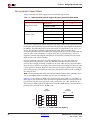
Note: Optional ports represented in italics
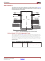
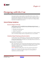
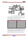
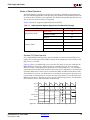
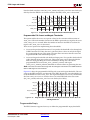
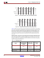
Figure 4-1: FIFO with Independent Clocks: Write and Read Clock Domains
For write operations, the write enable signal (WR_EN) and data input (DIN) are
synchronous to WR_CLK. For read operations, the read enable (RD_EN) and data output
(DOUT) are synchronous to RD_CLK. All status outputs are synchronous to their respective
clock domains and can only be used in that clock domain. The performance of the FIFO can
be measured by independently constraining the clock period for the WR_CLK and RD_CLK
input signals.
The interface signals are evaluated on their rising clock edge (WR_CLK and RD_CLK). They
can be made falling-edge active (relative to the clock source) by inserting an inverter
between the clock source and the FIFO clock inputs. This inverter is absorbed into the
internal FIFO control logic and does not cause a decrease in performance or increase in
logic utilization.
Initializing the FIFO Generator
When designing with the built-in FIFO or common clock shift register FIFO, the FIFO must
be reset after the FPGA is configured and before operation begins. An asynchronous reset
pin (RST) is provided, which is an asynchronous reset that clears the internal counters and
output registers.
For FIFOs implemented with block RAM or distributed RAM, a reset is not required, and
the input pin is optional. For these FIFO configurations, users have the option of
asynchronous or synchronous reset (only in common clock implementations). When
asynchronous reset is implemented, it is synchronized to the clock domain in which it is
used to ensure that the FIFO initializes to a known state. This synchronization logic allows
for proper reset timing of the core logic, avoiding glitches and metastable behavior. For
independent clock implementations, the synchronization process mandates a 3-cycle delay
post-reset prior to writing to the FIFO. For common clock implementations, a 2-cycle delay
post-reset prior to writing to the FIFO is mandated. For synchronous reset, no additional
40
www.xilinx.com
FIFO Generator v3.3 User Guide
UG175 April 2, 2007