1
Evaluation Board User Guide
UG-248
OPERATING MODES
95
The SSM2380 has three operating modes: I2C control mode,
ALC mode, and gain select mode. These modes are described
in detail in the SSM2380 data sheet. On the evaluation board,
the 3-pin JP11 jumper allows the user to change between the
available operating modes.
I2C CONTROL MODE
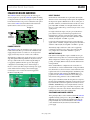
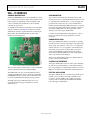
To operate the SSM2380 in I2C control mode, connect JP11 as
shown in Figure 5, connecting the MODE pin to GND. While
in I2C control mode, JP9 and JP10 are not used and the jumpers
should be left unconnected.
85
80
75
70
65
60
55
50
45
100
TYPICAL CONDITION
INTERNAL RESISTOR – 20%
INTERNAL RESISTOR + 20%
1k
10k
RESISTOR (Ω)
100k
1M
09686-007
OUTPUT VOLTAGE LIMIT (%)
90
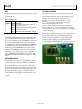
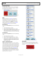
Figure 7. Output Voltage Limit (VTH) vs. RTH
Figure 5. Jumper Connections for I2C Mode Operation
ALC MODE
09686-006
The proper connections for ALC mode are shown in Figure 6.
For this setting, JP11 is open and the middle and bottom pins
of JP9 are shorted. This floats the MODE pin and makes a
connection from the SSM2380 ALCTH pin with Resistor
R24 to GND, setting the SSM2380 ALC limiting range. JP10
is used to activate the radiated emissions reduction mode in
this configuration.
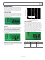
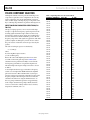
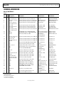
The proper connections for gain select mode are shown in
Figure 8. A jumper must be inserted on JP11 from center pin
to top pin. JP9 and JP10 allow the user to select the SSM2380
gain from 6 dB to 24 dB. To connect the appropriate gain select
pin to VDD, place a jumper from the center pin to the top pin
of the header. To select GND, simply move the jumper connection to the center pin and bottom pin of the header. A gain
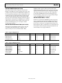
select table shows all possible settings in Table 2. All other
features (ALC, emissions control, and mixer) are deactivated
while the SSM2380 is in gain select mode.
09686-008
09686-005
GAIN SELECT MODE
Figure 6. Jumper Connections for ALC Mode Operation
Figure 8. Jumper Connections for Gain Select Mode Operation
Table 2. Gain Select Mode Settings for JP9 and JP10
The limiting percentage of the ALC feature is determined by the
value of an external resistor, R24, which should be placed on the
secondary side of the board. The resistor value can be calculated
using the curve shown in Figure 7.
GAIN1 (JP9)
GND
GND
VDD
VDD
Rev. 0 | Page 5 of 20
GAIN0 (JP10)
GND
VDD
GND
VDD
Gain Setting
6 dB
12 dB
18 dB
24 dB