1
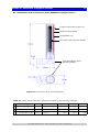
HDL
HIGHTECH
DEVELOPMENT
LEIDEN
User’s Manual
SRD1000 System
MIDS-10
ACS-10
adjustable DC current source
DCS-10
demagnetisation coil supply
TBX-10 testbox
SRD1000
mutual inductance detection system
supports precision thermometry on the PLTS-2000
User’s Manual SRD1000 System, version: 06-02-2006, HDL, Leiden, The Netherlands
For more information, please contact
HDL
P.O. Box 691
2300 AR Leiden
Contact:Dr. Ir. W.A. Bosch
Phone: + 31 (0)71 521 06 72
Fax:
+ 31 (0)71 523 69 16
E-mail: [email protected]
User’s Manual SRD1000 System, version: 06-02-2006, HDL, Leiden, The Netherlands
Contents
3
1. Introduction to the SRD1000 system
5
2. Installation system components
8
2.1. Handling the cryogenic sensor _________________________________________8
2.2. Mechanical and thermal connections
____________________________________8
2.3. Electrical connections ________________________________________________8
2.3.1. Signal connections _____________________________________________8
2.3.2. Signal parameters _____________________________________________9
2.3.3. Requirements for electro-magnetic shielding and filtering in the cryostat ___9
2.3.4. Connections from the sensor to the top part of the cryostat
___________10
2.3.5. Connections between the cryostat and the electronics ________________10
2.3.6. Testing the connections ________________________________________11
2.4. Measuring the signals _______________________________________________11
2.4.1. Connecting the electronics
_____________________________________11
2.4.2. Output signal versus sensor temperature
_________________________12
2.4.3. Testing the MIDS-10 system ____________________________________13
2.5. System map ______________________________________________________14
3. Realisation of the reference points
15
3.1. Experimental set-up ________________________________________________15
3.2. Degaussing the Cryoperm magnetic shield
3.3. Temperature and width of a reference point
3.4. Staircase patterned temperature sweep
______________________________15
_____________________________16
________________________________16
4. Residual magnetic field test at low temperatures
4.1. TC shifts due to magnetic fields
18
_______________________________________18
4.2. Test procedure for residual magnetic fields ______________________________18
4.2.1. Preparing the ACS-10
_________________________________________19
4.2.2. TC versus IDC measurements ____________________________________19
Annex A. SRD1000 cryogenic sensor
21
A1. The dimensions and connections of the sensor ____________________________21
Annex B. MIDS-10 mutual inductance detection system
22
B1. Features __________________________________________________________22
B2. Control unit, front panel
_____________________________________________22
B3. Control unit, rear panel ______________________________________________23
B4. Mains adapter
_____________________________________________________23
B5. Preamplifier unit
B6. Test box
___________________________________________________24
_________________________________________________________24
B7. Connections / cable arrangements
_____________________________________25
Annex C. DCS-10 demagnetisation coil supply / degauss coil
C1. Features
26
_________________________________________________________26
C2. Front / rear view ___________________________________________________26
User’s Manual SRD1000 System, version: 06-02-2006, HDL, Leiden, The Netherlands
Contents (continued)
Annex D. ACS-10 adjustable current source
D1. Features
4
27
_________________________________________________________27
D2. Front / rear / bottom view ___________________________________________27
Annex E. Symbols and definitions
User’s Manual SRD1000 System, version: 06-02-2006, HDL, Leiden, The Netherlands
28
1. Introduction to the SRD1000 system
The SRD1000 system comprises a cryogenic sensor and related measurement equipment to establish a series of reference points for thermometry between approximately 15 mK and 1.2 K.
The points are realised by observing superconductive transitions of a set of samples of reference materials using a mutual inductance detection technique.
An overview of the main system components:
(1) SRD1000 cryogenic sensor
The sensor contains a mutual inductance detector
array of integrated planar micro-coils to which
samples of various superconductive reference
materials are attached. The detector array and
the samples are thermally connected to a goldplated mounting plate at the bottom of the sensor.
The temperatures of the superconductive transition of the materials depend on the presence of a
magnetic field. To reduce ambient magnetic
fields, the sensor is equipped with a cylindrical
(Cryoperm / niobium) shield.
A compensation coil inside the shield surrounding
the detector assembly allows for additional testing and suppression of magnetic fields in the sensor.
The signal leads of the sensor are shielded and
equipped with a filter to suppress RF-interference.
The user has to attach the sensor to a thermal
plate inside the low temperature area of a cryogenic set-up and connect it to the room temperature MIDS-10 electronics via 3 pairs of (shielded)
twisted conductors.
Annex A. provides information on the dimensions
and the electrical connections of the sensor.
(2) MIDS-10 mutual inductance measurement system
The measurement system drives the cryogenic
sensor and provides an output voltage proportional to the sensor signal to detect the superconductive transitions.
The system comprises the following components:
- a control unit;
- a preamplifier unit to drive current to the primary coil input of the sensor and amplify the
voltage of the secondary coil output;
- a mains adapter for powering the MIDS-10;
User’s Manual SRD1000 System, version: 06-02-2006, HDL, Leiden, The Netherlands
5
1. Introduction to the SRD1000 system (continued)
- a test plug to verify the functioning of the preamplifier / control unit;
- a cable (grey, 5 m, 8-way Lemo 1B connectors)
to connect the preamplifier with the control
unit ;
- a cable (black, 0.75 m, 5-way Lemo 0B connector) to connect the preamplifier with the cryostat connector;
- a test unit (TBX-10) which converts ‘Lemo’ to
‘BNC’ and thus allows easy testing of the sensor
connections.
Annex B gives additional information on the
MIDS-010 system, explaining the controls and
terminals on the front and rear panels and the pin
layout of the cable connections.
(3) Calibration certificate
A calibrated cryogenic sensor and MIDS-10 system is supplied with a PTB certificate stating the
temperatures of the reference points.
Annex E lists the symbols and definitions that are
used to present the characteristics of the transitions.
(4) DCS-10 degauss tools
The DCS-10 supply unit with degauss coil enables
the demagnetisation of the Cryoperm magnetic
shielding of the cryogenic sensor at room temperature prior to a low temperature run.
Annex C presents additional information on the
DCS-10, describing the items on the front and
rear panels.
(5) ACS-10 current source
The ACS-10 adjustable current source is used to
test for residual magnetic fields in the sensor at
cryogenic temperatures.
The ACS-10 is supplied with:
- a cable (black, 0.75 m, 5-way Lemo 0B
connector) to connect the unit to the compensation coil in the sensor to reduce the Zcomponent of a residual magnetic field;
- a cable (black, 0.75 m, 5-way Lemo 0B connectors) to connect the unit to the preamplifier to
reduce the X,Y-components of a residual magnetic field;
User’s Manual SRD1000 System, version: 06-02-2006, HDL, Leiden, The Netherlands
6
1. Introduction to the SRD1000 system (continued)
- 9 V PP3 alkaline battery to power the current
source.
Annex D gives additional information on the ACS10, describing the items on the front and rear
panels.
User’s Manual SRD1000 System, version: 06-02-2006, HDL, Leiden, The Netherlands
7
2. Installation system components
8
This chapter provides an overview of the installation of the system components. Please refer to
Section 2.5 for a system map. The Annexes A to
D provide details on the features of the various
components.
Please e-mail HDL if you experience any problems
during the installation of the SRD1000 system.
2.1. Handling the cryogenic sensor
Figure 2.1 shows the SRD1000 cryogenic sensor.
The outer shield [1] of the cryogenic sensor is
made of annealed Cryoperm covered with a layer
of copper foil for thermal conduction. Avoid mechanical stress to this shield, as this may reduce
its shielding performance. Do not try to open the
sensor by removing the shield as you may damage the internal circuitry. Do not immerse the
sensor directly and quickly from room temperature and atmospheric conditions into liquid N2.
Always cool and warm it gradually and in a protected atmosphere, like in the IVC of a dilution
refrigerator. This will avoid severe internal stress
to the reference samples and the detection circuitry.
The electrical connections [5] are not sensitive to
electrostatic discharge. The resistance of the circuitry may be measured using a digital multimeter at ranges equal and below 20 MΩ.
5
1
4
2
3
Figure 2.1. The SRD1000 cryogenic sensor.
2.2. Mechanical and thermal connections
The mounting adapter [2], made of gold-plated
OFHC copper, is attached to a thermal plate in
the experimental region of a dilution refrigerator
using a (stainless steel) M3 bolt and washer. Prior
to mounting, remove any oxidation on the thermal plate when its surface is not gold plated, and
clean the contacting surfaces thoroughly with
acetone and alcohol to reduce the thermal resistance of the joint.
SRD1000 coil system
compensation
coil
detector coils with
reference samples
In most cases the filter [3] and the three shielded
leads [4] are mechanically (and electrically) fixed
at the same thermal plate as to which the sensor
is being attached. The thermal conduction of the
leads is low at cryogenic temperatures, as the
shield of the leads is made of phosphor-bronze
mesh and the internal conductors are of NbTi.
The leads are already thermally anchored inside
the sensor body.
2.3. Electrical connections
EMI-filter
2.3.1. Signal connections
P
The sensor contains a set of mutual inductors, the
red and blue coils in Figure 2.2, to detect the
transitions of the reference materials. A compensation coil (the green coil) allows reduction of residual magnetic fields in the sensor shield.
S
C
Figure 2.2. The sensor circuitry and
connections.
User’s Manual SRD1000 System, version: 06-02-2006, HDL, Leiden, The Netherlands
2. Installation system components (continued)
9
The coils are connected through 3 shielded superconductive leads. These are about 20 cm long
and each one contains a twisted pair of insulated
conductors.
A filter reduces spurious (EMI) signals entering
the sensor through the leads.
Each lead is terminated with a 2-way connector
(pin spacing 2.56 mm / 0.1”), see Figure 2.3,
which fits into a standard type IC socket (e.g. a
SIL-socket connector). The colour of the tubing
indicates the type of connection (P, primary coil
= red; S, secondary coil = blue; C, compensation coil = green).
Table A.1 in Annex A summarizes the connections
and lists general values for the electrical resistance of the coils at 300 K, 77 K and at T < 9 K.
The label on the transport box of the sensor gives
the specific values.
Figure 2.3. The P, S and C connectors.
At room temperature, the resistance between the
primary and secondary circuitry should be higher
than a few MΩ. This also applies for the resistance between the circuitries and the sensor
housing.
2.3.2. Signal parameters
The signal parameters of the sensor are:
(1) primary current: 50 µA @ 976.5 Hz, producing a field of less than 0.4 µT near the reference samples;
(2) secondary voltage: 2 nV – 2 µV, depending
on the temperature of the sensor;
(3) compensation coil current: 0 - ± 2 mA, producing a field of about 0 – ± 5 µT near the
samples.
2.3.3. Requirements for electro-magnetic
shielding and filtering in the cryostat
The amplitude of the AC field produced by the
sensor detection circuitry is negligible outside the
sensor shielding («100 nT). The SRD1000 measurement electronics was designed for use in ultralow temperature set-ups and have proved not to
cause RF-heating or other interference in cryogenic experiments.
The sensor is equipped with a filter to reduce RFenergy penetrating the sensor housing. Additional
filtering of sensor signal leads in the cryostat may
lead to phase shifts and distortions while measuring the transitions of the device. However, the
effects of small capacitors (< 0.2 nF) and ferrite
chokes are negligible.
For specific cases, please contact HDL.
User’s Manual SRD1000 System, version: 06-02-2006, HDL, Leiden, The Netherlands
2. Installation system components (continued)
10
2.3.4. Connections from the sensor to the
top part of the cryostat
For optimal results use 3 separate cables in the
cryostat to connect the primary, secondary and
compensation coils of the sensor. Preferably, one
should use a shielded twisted pair cable for each
connection. In the section of the cryostat at temperatures below 9 K this should preferably be superconductive cable. Ensure proper thermal anchoring at various suitable points in the set-up.
Small diameter (about ∅ 1 mm) superconductive
or normal conductive shielded twisted pair cable
made by Habia is obtainable through HDL (Figure
2.4). Similar types are available from other companies, like Lake Shore.
Figure 2.4. Cryogenic shielded twisted
pair cable.
The DC resistance of each lead of a connection to
the sensor should be less than about 50 Ω when
the cryostat is at cryogenic temperatures.
2.3.5. Connections between the cryostat and
the electronics
The electronics are supplied with 2 (black)
shielded cables (Figure 2.5) for the room temperature connections to the cryostat:
(1)
(2)
mutual inductance cable for connecting the
MIDS-10 preamplifier;
compensation coil cable for connecting the
ACS-10 current source.
Figure 2.5. Black cable with 5-way
Lemo 0B connector.
(1) ground
Each cable is about 0.75 m long and contains 3
shielded twisted pair conductors.
One side is terminated with a 5-way Lemo 0B free
plug, the connector at the other side of the cable
has to be selected by the user to fit the connector
at the top part of the cryostat.
Figure 2.6 gives the pin layout for the Lemo connector and Table 2.2 shows the connection
scheme of the cables. The shields of the cables
are to be connected to the ground/chassis of the
cryostat.
(2) V+
(5) I- / C-
(4) V-
(3) I+ / C+
Figure 2.6. Pin layout of the 5-way
Lemo 0B connector (front view of the
male free plug or rear (solder) contact
view of the female chassis socket). The
yellow line indicates the direction of the
pin number count.
Table 2.2.
Lemo 0B lead colour
pin #
(1)
yellow / green
(2)
white
(3)
violet
(4)
brown
(5)
grey
mutual inductace
connection (1)
ground / shield
secondary coil V +
primary coil I +
secondary coil V primary coil I -
compensation coil
connection (2)
ground / shield
current C+
current C-
User’s Manual SRD1000 System, version: 06-02-2006, HDL, Leiden, The Netherlands
2. Installation system components (continued)
11
2.3.6. Testing the connections
After the installation of the sensor and the signal
leads it is important to verify that all connections
are made correctly before the sensor circuitry becomes superconducting.
If, for example the connection to the primary coil
is accidentally interchanged with the one to the
secondary coil, the sensor may seem to operate
correctly at low temperatures. However, in this
case the primary current is running in the secondary coil, producing a magnetic field near the reference samples that is a factor 10 higher than
during normal operation. Consequently the superconductive transitions are shifted to lower temperatures.
P
S
SRD
Figure 2.7. TBX-10 test box.
The connections can be verified by checking the
resistance values of the coils at the Lemo 0B’s
connectors outside the cryostat.
1
The TBX-10 test box (Figure 2.7) facilitates these
checks by converting the Lemo 0B connections to
BNC terminals clearly marked with ‘primary
coil’ [P] and ‘secondary coil’ [S].
3
2
4
5
Figure 2.8. MIDS-10 preamplifier unit.
2.4. Measuring the signals
2.4.1. Connecting the electronics
The MIDS-10 system is designed for use at room
temperature in a laboratory environment. Refer
to Annex B for more information regarding the
system components.
Position the MIDS-10 preamplifier unit (Figure
2.8) near the top of the cryostat and connect the
cryogenic sensor to the preamplifier unit using
the black interconnecting cable (see section 2.3).
Ensure that the preamplifier is not too close to a
source of electro-magnetic interference, such as a
mains transformer of another instrument.
Position the MIDS-10 control unit (Figure 2.9) at
a convenient position to monitor the SRD1000
signal.
Connect the preamplifier (terminal [2]) to the
control unit (terminal [12]) using the 5 m grey
cable (Figure 2.10). Ensure that the 8-way Lemo
1B connectors at both ends of the grey cable are
firmly plugged in all the way (a clicking sound is
heard when the connector snaps into its mechanical restraint).
Connect the mains adapter (Figure 2.11) to the
mains supply and to the control unit (terminal
[6]).
1
2
3
4
5
Figure 2.9a. MIDS-10 control unit,
front panel.
6
7
8
9
10
11
12
13
Figure 2.9b. MIDS-10 control unit,
rear panel.
Figure 2.10. Grey cable with 8-way Lemo 1B
connector.
Figure 2.11. MIDS-10
mains adapter.
User’s Manual SRD1000 System, version: 06-02-2006, HDL, Leiden, The Netherlands
2. Installation system components (continued)
12
Switch on the power switch [5] of the control unit
(the blue power LED’s at both the control and
preamplifier unit are on). Set the primary current
switch [1] to ‘off’, the filter switch [2] to ‘fast’,
and display switch [3] to ‘output’ (blue display
LED is on). The front panel meter should settle
down at about 000.
When the cryogenic sensor is at temperatures below 9.5 K, its circuitry is superconducting and one
can switch the primary current switch [1] to ’on’.
The front panel meter should settle at a value between 500 and 1000, which equals the system
output voltage in mV. If the display shows a
negative sign, reverse the phase +/- switch [13]
at the rear of the MIDS-10 unit.
Set the filter switch [2] to ‘slow’ for normal operation at a low noise level (the time constant of
the system output voltage is about 62.5 s).
2.4.2. Output signal versus sensor temperature
The voltage level depends on the temperature of
the cryogenic sensor, see Figure 2.12 for a typical
example. It varies from about 550 mV at a temperature T < 15 mK to about 850 mV at T > 1.2
K.
The ten steps of the staircase pattern are at the
ten superconductive transitions of the reference
samples. The height of a transition step varies
between about 5 mV to 100 mV depending on the
sample.
AuIn2
Output voltage [V]
The output signal of the system is a DC voltage at
the output terminal [11] located at the rear panel
of the control unit.
0.850
0.800
AuAl2
Cd
Zn
Al
Ir
0.750
0.700
Ir92Rh08
Ir80Rh20
0.650
0.600
Be
W
0.550
10
100
1000
Temperature [mK]
Figure 2.12. Output voltage control unit
as a function of the temperature of the
cryogenic sensor.
The noise present in the signal is about 0.4 mV
peak-to-peak, when the filter of the control unit is
set to ‘slow’.
To record the signal with a computer, use for example a DVM with a resolution of at least 0.1 mV
at a full range of 2 V, equipped with a computer
interface.
Please be aware of the influence (like heating effects) that such digital meters and interfaces may
produce on low temperature set-ups due to the
generation of RF-energy.
Whenever possible, apply an optical interface between the computer and the measuring equipment to reduce such interference problems.
User’s Manual SRD1000 System, version: 06-02-2006, HDL, Leiden, The Netherlands
2. Installation system components (continued)
13
2.4.3. Testing the MIDS-10 system
In order to test the basic transfer function of
MIDS-10 electronics, one can connect the test
plug to the preamplifier instead of the cryogenic
sensor (Figure 2.13).
At the control unit, set the primary current switch
[1] to ‘on’, the filter switch [2] to ‘slow’ and display switch [3] to ‘output’. This should produce a
voltage value at the output terminal [11] as is
indicated on the test plug. The value displayed on
the front panel meter may deviate ± 1 LSB from
this value.
Figure 2.13. The test plug connected to
the preamplifier; the control unit displays
the value as indicated on the plug.
To test the performance of the front panel meter,
set the primary current switch [1] to ‘off’ and turn
the offset control knob [4] fully clockwise.
When the display switch [3] is set to:
- ‘output’, the meter should read 000,
- ‘offset’, it should read 1000,
- ‘deviation’, it should read –1000
(all indications are ± 1 LSB).
An oscilloscope connected to the signal monitor
terminal [9] enables the observation of the amplified AC signal of the sensor or test plug.
Figure 2.14. Sensor and sync signal
displayed on an oscilloscope.
The signal should be sinusoidal with a frequency
of about 977 Hz and its amplitude varies somewhat due to noise of the preamplifier (see Figure
2.14). The sync output terminal [8] provides a
square wave signal to trigger the oscilloscope.
preamplifier unit
Connect the SRD terminal [1] of the preamplifier
to the test box using the black Lemo 0B cable
supplied with the ACS-10 unit.
One can measure the current at the primary coil
terminal [P] of the test box with a true-RMS type
current meter. The meter preferably should be
powered by a battery and not by the mains supply. The effective value of the current should be
50 µA ±1% (@ 977 Hz).
test box
S
T B X -1 0 t e s t b o x
Figure 2.15 shows a set-up for testing the effective value of the AC primary current.
P
control unit
50.0 µA
true-RMS type
current meter
Figure 2.15. Testing the primary
current.
User’s Manual SRD1000 System, version: 06-02-2006, HDL, Leiden, The Netherlands
2. Installation system components (continued)
14
2.5. System map
test box (Section 2.3.6, Annex B6)
T B X -1 0 t e s tb o x
resistance meter (Section 2.3.6)
current meter (Section 4.2.1)
ACS-10 (Section 4.2.1, Annex D)
ACS-10
adjustable DC current source
test plug
(Section 2.4.3)
MIDS-10 preamplifier unit
(Section 2.4.1, Annex B5)
5-way black
cables
(Annex B7)
8-way grey cable
(Annex B7)
oscilloscope (Section 2.4.3)
cryostat connector
(Section 2.3.5, Annex B7)
cryostat
system
normal conductive
shielded twisted pairs
MIDS-10 control unit
(Section 2.4.1, Annex B2/3)
thermal anchoring /
connector
MIDS-10
T > 9 K level
mutual inductance detection system
T < 9 K level
MIDS-10 mains adapter
(Section 2.4.1, Annex B4)
superconductive shielded
twisted pairs (Section 2.3.4)
thermal anchoring
digital voltmeter
(Section 2.4.2)
DMM
computer
cryogenic sensor
(Section 2.3,
Annex A)
optical interface
EMI-filter
SRD1000
DCS-10
(Section 3.2, Annex C)
DCS-10
demagnetisation coil supply
thermal plate: 14 mK < T < 1.2 K
User’s Manual SRD1000 System, version: 06-02-2006, HDL, Leiden, The Netherlands
3. Realisation of the reference points
3.1. Experimental set-up
15
mixing chamber
Figure 3.1 shows a set-up typical for the realisation of the reference points of the SRD1000 cryogenic sensor.
The sensor is attached to a thermal plate together with some thermometers. The plate is
connected to the mixing chamber of a dilution refrigerator with a heat link. A heater is attached to
the link for temperature regulation. In order to
reduce thermal gradients within the plate, the
heater is not positioned at the plate itself. One of
the thermometers is used to provide a PIDfeedback loop to control the heater power. A
thermal shield surrounding the set-up reduces
gradients produced, for example, by thermal radiation or residual exchange gas.
Make sure that the thermal resistance of the
pressed contact between the mounting adapter of
the sensor and the thermal plate is as low as possible. Especially at temperatures below 50 mK the
heat flow from / to the Cryoperm shield of the
sensor may otherwise lead to significant (timedependent) temperature differences between the
sensor and the thermal plate and thus to errors in
the realisation of the reference points. Always
clean the contacting surfaces with acetone and
alcohol before the joint is made. If the thermal
plate is not gold-plated, first remove any oxide
layer by gently polishing the contact area.
heat link
thermal
shield
heater
sensor
thermometers
SRD1000
Cryoperm
shield
mounting
adapter
thermal plate
Figure 3.1. Set-up for thermometry
with the SRD1000 cryogenic sensor.
Figure 3.2. DCS-10 and the degauss coil.
3.2. Degaussing the Cryoperm magnetic
shield
The strength of ambient magnetic fields at the
mounting position of the sensor should be in the
order of 100 µT or less (the earth magnetic field).
In order to obtain an optimal shielding performance at low temperatures, the Cryoperm shield
should be degaussed at room temperature using
the DCS-10 unit and the degauss coil (Figure
3.2.) prior to each low temperature run.
1
Do not forget to switch off the DCS-10 after the
procedure. The supply unit and coil may become
warm after prolonged use. This is a normal situation. Do not cover the supply unit to prevent
overheating.
4
3
5
Figure 3.3. Front and rear view of the
DCS-10.
Proceed by connecting the degauss coil to the
DCS-10 supply unit (terminal [1], Figure 3.3).
Next, connect the DCS-10 to the mains supply
(cable [5]) and switch on the unit (switch [4], the
blue LED [3] is on).
Move the degauss coil slowly starting from about
5 cm above the Cryoperm shield downwards and
then upwards again (see Figure 3.4. a, b, c, d, e).
The total sequence should take about 20 s. Repeat the sequence at least one more time.
2
degauss coil
about 5 cm
SRD1000
a
SRD1000
b
SRD1000
c
SRD1000
d
SRD1000
e
Figure 3.4. Degauss sequence Cryoperm
shield.
User’s Manual SRD1000 System, version: 06-02-2006, HDL, Leiden, The Netherlands
3. Realisation of the reference points (continued)
16
3.3. Temperature and width of a reference point
VNC* = 42.5 mV
A reference point is observed by monitoring the
output voltage V(T) of the MIDS-10 electronics as
a function of the temperature T of the cryogenic
sensor.
V90* = 38.3 mV
30
V * [mV]
Figure 3.5 shows an example of the superconductive transition of an Ir92Rh08 sample.
40
When the temperature is increased, the state of
the reference sample in the sensor gradually
changes from the superconducting state, corresponding to a system output voltage V = VSC, to a
state of normal conducting, with V = VNC.
In this manual reduced output voltages V* relative to voltages in the superconducting state are
used to present the data of the transitions, with
V* = V - VSC .
TC = 65.34 mK
VC* = 21.3 mV
20
WC = 0.24 mK
10
V10* = 4.3 mV
0
63
64
65
66
67
T2000 [mK]
Figure 3.5. Superconductive transition
of an Ir92Rh08 sample.
The reference point TC is defined as the temperature when 50% of the transition is completed,
which is at V(TC) = 0.5 (VNC +VSC). Relative to the
superconducting state this it at:
VC* = V*(TC) = V(TC) - VSC = 0.5 (VNC - VSC ).
For many transitions the most temperaturesensitive part occurs when the signal level is between approximately 10% and 90% of the interval VNC - VSC . The corresponding temperature interval is defined as the width WC of the transition:
WC = T (V90*) – T (V10*), with V90* = 0.9 VNC*
and V10* = 0.1 VNC* .
The transition of Figure 3.5 shows a width WC of
0.24 mK and provides a reference point at TC =
65.34 mK with VC* = 21.3 mV.
Annex E gives an overview of the symbols and
definitions to present the characteristics of a transition.
67.0
3.4. Staircase patterned temperature
sweep
This means that each time temperature T is increased with a step ∆T, next, during a stabilisation time ∆t, the temperature is stabilised at
T+∆T before a next ∆T step is made.
66.0
T2000 [mK]
In order to observe a transition, preferably a
staircase pattern is used to increase the temperature of the thermal plate, see Figure 3.6.
66.5
65.5
65.0
64.5
64.0
63.5
The interval ∆t has to be sufficiently long to establish thermal equilibrium between all relevant
elements at the thermal plate before the data
point at T+∆T is collected.
0
100
200
300
400
500
time [ minutes]
Figure 3.6. Temperature sweep following
a staircase pattern.
User’s Manual SRD1000 System, version: 06-02-2006, HDL, Leiden, The Netherlands
3. Realisation of the reference points (continued)
In order to reproduce a transition with sufficient
resolution at least 5 data points are to be measured along the most temperature-sensitive part
of the transition.
This means that step ∆T should be smaller than
WC / 5. It also means that the stability of the
temperature regulation during the sweep should
be (significantly) better than WC / 5.
Remark. Figure 3.6 shows the staircase pattern
of the temperature sweep between about 64 mK
and 67 mK that was used during a calibration run
to record the transition of Figure 3.5. The size of
each ∆T step of the staircase is about 60 µK and
the period ∆t after a step is about 10 minutes.
Depending on the thermal characteristics of a setup and the desired accuracy level of the reproduction of TC different settings for ∆T and ∆t
might be used.
User’s Manual SRD1000 System, version: 06-02-2006, HDL, Leiden, The Netherlands
17
4. Residual magnetic field test at low temperatures
18
4.1. TC shifts due to magnetic fields
The TC value of a reference sample is reduced by
the presence of a magnetic field. Tabel 4.1 presents estimated values for the shift dTC / dB of
each type of sample material.
Experimental work has shown that the magnetic
shielding of the sensor sufficiently reduces common ambient magnetic fields in a cryostat once
the shield is properly degaussed at room temperature before the start of a low temperature
experiment (see Section 3).
However, in order to reproduce the reference
points with the highest accuracy, one should verify that residual fields in the sensor are sufficiently low.
4.2. Test procedure for residual magnetic fields
Figure 4.1 shows the shield and coil configurations of the cryogenic sensor.
Table 4.1. Shift dTC / dB of the reference
materials.
#
Material
1
2
3
4
5
6
7
8
9
10
W
Be
Ir80Rh20
Ir92Rh08
Ir
AuAl2
AuIn2
Cd
Zn
Al
[1] J.R. Schooley et al., Temperature, Its Control
and Measurement in Science and Industry, 5,
p. 251-260, 1982;
[2] Estimated value based on measurements on
Ir92Rh08 samples [3];
[3] W.A. Bosch et al., Measurements on the
SRD1000 reference materials, Kamerlingh Onnes Laboratorium, Leiden, 2005.
An electrical current running in the detector coils
(green squares) will generate a magnetic field in
the X,Y-plane (horizontal component). A current
in the compensation coil (red cylinder) will result
in a magnetic field in the Z-direction (vertical
component).
The ACS-10 current source is a tool which allows
an adjustable DC current to run either in the detector coils, superimposed on the AC primary current to analyse the horizontal (X,Y) component,
or in the compensation coil to analyse the vertical
(Z) component. Please note that the ACS-10 does
not provide for testing a combination of the horizontal and vertical components at the same time.
Experimental work proved that in most cases,
due to the geometry of the shielding, the X,Ycomponents are significantly smaller than the Zcomponent. Thus analysing only the Z-component
will generally suffice for the residual field test.
By varying the strength and the sign of the current while operating the cryogenics sensor and
observing a transition, one can find a value for
the current at which a residual magnetic field
near the samples is reduced or compensated.
TC
dTC /dB Ref.
[mK] [mK/µT]
15
-0.09
[1]
21
-0.14
[1]
30
-0.03
[2]
65
-0.03
[3]
98
-0.09
[3]
145
-0.10
[3]
208
-0.16
[3]
520
-0.14
[3]
850
-0.06
[3]
1180
-0.06
[1]
Cryoperm cylinder shield
Niobium shield
Compensation coil
SRD copper body
SRD detector coil on chip
I
detector coil
Z
Bcomp
X
Bdet
Y
I
compensation coil
Figure 4.1. Shield and field configurations
of the cryogenic sensor.
Please note that connecting the ACS-10 current
source to the sensor circuitry should only be done
for an occasional field test. For standard operation to reproduce the reference points it is advised to disconnect the ACS-10.
User’s Manual SRD1000 System, version: 06-02-2006, HDL, Leiden, The Netherlands
4. Residual magnetic field test at low temperatures (cont.)
19
4.2.1. Preparing the ACS-10
Before using the ACS-10 (see Figure 4.2) insert a
9V PP3 battery in the bottom compartment. When
the on/off switch [4] is operated, the blue power
LED [3] should go on and off, if not the battery
voltage is too low.
Connect a DC current meter (e.g. a digital multimeter) at the BNC output [6]. In order to activate
this output, set the monitor output switch [7] in
the 'on' position.
1
2
3
Figure 4.2a. ACS-10, front view.
- To test for the Z-component of the residual
field, connect the compensation coil input [C]
of the cryogenic sensor to the current output
[5] at the rear of the ACS-10, see Figure 4.3.
(a);
4
- To test for X,Y-components, connect the input
marked 'ACS-10' at the preamplifier unit to the
current output [5] at the rear of the ACS-10
using the black cable supplied with the ACS-10,
see Figure 4.3. (b).
4.2.2. TC versus IDC measurements
To determine the residual field component one
has to measure the shift of TC as a function of the
ACS-10 current IDC in the sensor.
The AuAl2 transition is well suited for these measurements. The transition at about 145 mK is located in a temperature region where most dilution refrigerators work well and where temperature control is often easy. The transition is also
smooth and narrow, and the midpoint is easily
determined.
Two methods are possible, each requiring different skills from the operator:
6
7
Figure 4.2b. ACS-10, rear view.
cryostat connector
C
cryostat connector
P,S
C
P,S
preamp
preamp
MIDS-10
preamp
MIDS-10
preamp
(a)
(b)
control unit
control unit
Figure 4.3. Connecting the ACS-10,
see the text.
530
IDC = 0.0 mA, TC = 142.98 mK
IDC = 0.5 mA, TC = 142.87 mK
IDC = 1.0 mA, TC = 142.72 mK
IDC = 2.0 mA, TC = 142.44 mK
520
V [mV]
Remark. One can check the performance of the
ACS-10 by inserting the test plug (see Section
2.5) in output [5]. Next switch the unit on and
turn knob [2] fully clockwise. The current meter
should read +2 mA or –2 mA depending on the
position of switch [1]. Note that the indication of
the ten-turn dial has to be multiplied by a factor 2
to find the setting of the output current, so for
example ‘500’ gives an output of 1 mA.
5
510
VC
500
490
(1) stabilise the temperature to reach the midpoint of the transition, apply a current IDC and adjust the temperature of the thermal plate so that
the midpoint is indicated again, then go for the
next current setting, adjust the temperature, etc.
(2) make various temperature sweeps (staircase
patterned, like in Figure 3.6) through the midpoint, each time for a different current setting IDC.
Figure 4.4 shows an example: for each IDC setting
a TC value is found at V = VC .
480
142.0
142.5
143.0
143.5
T [mK]
Figure 4.4. Example of an AuAl2 transition
observed for various currents settings.
User’s Manual SRD1000 System, version: 06-02-2006, HDL, Leiden, The Netherlands
4. Residual magnetic field test at low temperatures (cont.)
Method 2 is more time-consuming, but often easier to perform as the demands for the temperature stabilisation are easier to meet.
(TMAX , IRES)
The goal for each method is to acquire transition
data to determine the various TC values for several settings of IDC .
(T-100 , -100 µA)
Analyse the collected data by making a graph of
the observed TC and IDC values, like in Figure 4.5.
Find the intersection point of the blue and red
lines, corresponding to the maximum TC value
TMAX and the current value IRES.
One can derive the residual magnetic field BRES
near the tested sample by multiplying the value
IRES by the material-dependent coil constant that
can be found in Table 4.2.
The coil constants were derived both by calculations and experiments. Experimental work on the
value of the coil constants is still in progress and
future results shall be reported to the user.
-200
-100
0
100
200
I DC [µA]
Figure 4.5. Example of TC values as a
function of applied current IDC .
Table 4.2. Coil constants cryogenic sensor.
# Material
1
2
3
4
5
6
7
8
9
10
W
Be
Ir80Rh20
Ir92Rh08
Ir
AuAl2
AuIn2
Cd
Zn
Al
Coil constant Coil constant
XY-field
Z-field
[µT/µA]
[µT/µA]
6 . 10-3
2.5 . 10-3
.
-3
6 10
2.5 . 10-3
.
-3
6 10
2.7 . 10-3
.
-3
6 10
2.8 . 10-3
.
-3
6 10
2.6 . 10-3
.
-3
6 10
2.7 . 10-3
.
-3
6 10
2.8 . 10-3
.
-3
6 10
2.9 . 10-3
.
-3
6 10
2.7 . 10-3
.
-3
6 10
2.5 . 10-3
δT = 39 µK
0.05
0.00
∆TC [mK]
Example. Figure 4.6 shows an example of a
measurement of the shift ∆TC of an AuAl2 sample
versus the current IDC in the compensation coil,
with: ∆TC = TC (IDC) - maximum TC value. The position of the measured data points (marked ‘+’)
deviates from the blue and red straight lines for
|IDC| < 300 µA. The intersection point of the lines
is assumed to indicate the TC value of the sample
in zero magnetic field. The shift δT of 39 µK between this value and the top of the set of date
points is supposed to be caused by the AC detection field near the sample, which has an amplitude of about 0.3 µT. The IDC value at the intersection point of the lines is close to zero, which
indicates that the residual DC magnetic field near
the sample is negligible.
(T100 , 100 µA)
(T0 , 0 µA)
TC [mK]
For example, start by setting IDC at 0 µA and find
TC (0 µA) = T0, next set IDC at 100 µA to find T100,
switch to -100 µA for T-100 , next to -200 µA, +
200 µA, etc.
20
-0.05
-0.10
-0.15
-0.20
dTC / dIDC =
- 0.3 µK / µA
-800 -600 -400 -200
0
200
400
600
800
IDC [µA]
Figure 4.6. Shift ∆TC of an AuAl2 sample
versus IDC in the compensation coil
(measurements by the PTB institute).
User’s Manual SRD1000 System, version: 06-02-2006, HDL, Leiden, The Netherlands
Annex A. SRD1000 cryogenic sensor
21
A1. Dimensions and connections of the SRD1000 cryogenic sensor
Cryoperm shield with copper foil
internal niobium shield
compensation coil
coil system with reference samples
gold-plated OFHC copper
mounting adapter
Figure A1. The sensor and its outer dimensions.
Table A1. Sensor signal connections with general values for the electrical resistance.
# Connection type
Function
Colour code
R (300 K)
R (77 K)
R (< 9 K)
1
P (primary coil)
I+ , I-
red (+ = white)
180.000 Ω
90.000 Ω
0Ω
2
S (secondary coil)
V+ , V-
blue (+ = white)
700.000 Ω
350.000 Ω
0Ω
3
C (compensation coil)
C+ , C-
green
38 Ω
19 Ω
0Ω
User’s Manual SRD1000 System, version: 06-02-2006, HDL, Leiden, The Netherlands
Annex B. MIDS-10 mutual inductance detection system
22
B1. Features
- detection electronics to establish the temperature reference points of the cryogenic sensor;
- 'plug and play'; no adjustments are required for
the entire temperature range of the sensor;
- primary current: 50 µA @ 976.5 Hz;
- system voltage output : 0 - 1000 mVDC proportional to the sensor signal;
- temperature coefficient of the parameters of the
electronics: < 50 ppm/°C;
- design ensures minimal RF-heating in ultra-low
temperature experiments.
B2. Control unit, front panel
1
2
3
4
5
Item Description
Position
[1]
primary current switch
on*) / off
[2]
filter switch
slow*) / fast filter time constant of the system output [11] (rear panel)
is set to ‘slow’ (т = 62.5 s) or ‘fast’ (т = 10 s); the normal
operation mode is ‘slow’. The noise level of the signal at
the system output at ‘slow’ is about 0.4 mVpp, at ‘fast’
this is about 0.9 mVpp
[3]
display
switch
output*)
front panel meter shows the voltage VOUT [mV] at the system output [11] (blue output LED is on)
offset
front panel meter shows the set-point of the offset voltage
VOFF [mV] (blue output LED is off)
deviation
front panel meter shows the voltage VDEF = VOUT - VOFF
[mV] at the deviation output [10] (blue output LED is off)
10-turn
changes the level of the offset voltage VOFF (0 - 1000 mV)
[4]
[5]
offset control
power switch
*)
on
*)
/ off
Function
primary current (50 µA @ 976.5 Hz) is switched on or off;
the ‘off’ position may be used to diagnose heating effects
of the sensor, or to monitor possible interference at the
system output
power of the MIDS-10 main unit and preamplifier unit is
switched on or off, as is indicated by the blue power LED’s
default setting for normal operation
User’s Manual SRD1000 System, version: 06-02-2006, HDL, Leiden, The Netherlands
Annex B. MIDS-10 (continued)
23
B3. Control unit, rear panel
6
7
8
9
10
11
12
13
Item
Description
Function
[6]
power-in terminal (3-way male
socket, Binder
type 711 )
power input 8 V~, 50 mA max, 50 / 60 Hz (pin 1-3 or pin 1-2 depending on the regional voltage of the mains supply); only use the
mains adapter that is supplied for powering the MIDS-10 system to
avoid any damage to the electronics
[7]
ground (4 mm)
socket
terminal to ground the main unit (grounding is not required in most
cases)
[8]
sync output
(BNC)
AC square wave signal (1 VPP, f = 976.5 Hz) to synchronise an oscilloscope while monitoring the sensor signal [9]
[9]
signal monitor
output (BNC)
AC amplified secondary voltage of the sensor (f = 976.5 Hz) to be
monitored on a oscilloscope for diagnoses purposes
[10]
deviation output
(BNC)
DC deviation voltage VDEV = VOUT - VOFF to monitor small changes in
the system output voltage [11] relative to the set-point of the offset
voltage [4]
[11]
system output
(BNC)
DC output VOUT (0 - 1000 mV) proportional to the secondary voltage
of the sensor
[12]
preamp terminal
(8-way Lemo 1B
female socket)
to connect the 5m grey cable leading to the preamplifier unit
[13]
phase +/- switch to change the phase of the sensor signal by 180º when the front
panel meter shows a negative sign; for normal operation select a setting that will result in a positive sign on the meter; note that as VOFF
is a positive voltage, only a positive VOUT can be fully compensated by
VOFF at the deviation output
B4. Mains adapter
Power supply connection:
3-way female socket, Binder type 712
(nr. 99-0406-00-03).
Pin lay-out:
front view of the male panel socket or
solder contact view of the female cable
socket; the lead colour codes of the
supply cable are indicated.
2
The mains adapter.
3
1
Pin 1-3: 7.3 V~ @ input 230 V~ / 50 Hz / 7 VA;
Pin 2-3: 8.3 V~ @ input 230 V~ / 50 Hz / 2 VA;
Pin 1-2: 7.8 V~ @ input 115 V~ / 60 Hz / 7 VA.
User’s Manual SRD1000 System, version: 06-02-2006, HDL, Leiden, The Netherlands
Annex B. MIDS-10 (continued)
24
B5. Preamplifier unit
1
3
2
Item Description
4
5
Function
[1]
sensor terminal (5way Lemo 0B female socket)
to connect the black cable from the cryostat connection to the
sensor
[2]
control unit terminal (8-way Lemo
1B female socket)
to connect the 5 m grey cable leading to the control unit
[3]
power LED
indicates the power status of the preamplifier; when connected to
the main unit, the preamplifier unit is switched on / off by switch
[5] at the control unit
[4]
ACS-10 input terminal (5-way Lemo
0B female socket )
refer to Section 4.2; this input is used to connect the black cable
leading to the ACS-10 current source for analysing X,Y magnetic
field components in the sensor
[5]
4 mm ground
socket
terminal to ground the preamplifier unit (grounding is not required
in most cases)
B6. Test box
P
SRD
Item
S
Description / function
[SRD] input terminal (5-way Lemo 0B) for the black sensor cable from the cryostat in order
to test the electrical connections to the sensor
[P]
BNC connection to the primary coil section of the SRD connector: BNC shield -> Lemo
pin 5 (I-), BNC centre pin -> Lemo pin 3 (I+); connecting a resistance meter allows
the checking of the primary coil connections of the sensor
[S]
BNC connection to the secondary coil section of the SRD connector: BNC shield ->
Lemo pin 4 (V-), BNC centre pin -> Lemo pin 2 (V+); connecting a resistance meter
allows the checking of the secondary coil connections of the sensor
User’s Manual SRD1000 System, version: 06-02-2006, HDL, Leiden, The Netherlands
Annex B. MIDS-10 (continued)
25
B7. Connections and cable arrangements
Pin layout of the 5-way Lemo 0B connector and the composition of the black connecting cables.
(1)
(5)
(2)
(4)
(3)
Contact
Front view of the male
free plug or rear / solder contact view of the
female chassis socket;
the yellow line indicates
the direction of the pin
number count.
Lead colour
Mutual inductance
connection
(1)
yellow / green
ground / shield
(2)
white
secondary coil
(3)
violet
primary coil
(4)
brown
secondary coil
(5)
grey
primary coil
Compensation
coil connection
ground / shield
V+
I+
VI-
current C+
current C-
Pin layout of the 8-way Lemo 1B connector and the composition of the grey cable between
preamplifier and control unit.
(1)
(2)
(7)
(8)
(6)
(3)
Contact
(4)
(5)
Front view of the female
chassis socket or solder contact view of the male free
plug; the yellow line indicates the direction of the pin
number count.
Lead colour Connection
(1)
blue
ground
(2)
brown
sensor current reference +
(3)
white
sensor current reference -
(4)
violet
- 5 V supply
(5)
grey
ground / spare
(6)
yellow
amplified sensor voltage +
(7)
green
amplified sensor voltage -
(8)
red
+ 5 V supply
User’s Manual SRD1000 System, version: 06-02-2006, HDL, Leiden, The Netherlands
Annex C. DCS-10 demagnetisation coil supply / degauss coil
26
C1. Features
- tool for degaussing the Cryoperm shielding
of the sensor to optimise its magnetic properties;
- supply provides 1.7 A, 50 - 60 Hz to drive
the degauss coil;
- input 230 - 240 V / 50 Hz, (model a) or
115 V, 50 - 60 Hz, (model b), max. 10 W.
C2. Front / rear view
1
2
3
4
5
Item Function
[1]
AC current output to connect the degauss coil (5-way female socket, Binder type 711 )
[2]
fuse holder (contains 2 AT glass fuse, 20 x 5 mm) to limit the output current
[3]
blue power LED is on indicates that the output circuitry is on. When the degauss coil is
not connected, the LED shines bright, it dims when the coil is connected
[4]
power on / off switch
[5]
mains input 115 or 240 V / 50 - 60 Hz (depending on the model), 10 W max
User’s Manual SRD1000 System, version: 06-02-2006, HDL, Leiden, The Netherlands
Annex D. ACS-10 adjustable current source
27
D1. Features
- battery-powered precision current source for
compensating residual fields in the cryogenic
sensor;
- DC output current adjustable between 0 µA and
2000 µA with a polarity selection for the sign of
the output current;
- the compliance voltage is about 3 V;
- temperature coefficient electrical parameters:
smaller than 50 ppm/°C;
- the low load capacitance allows direct superimposing of the DC output current on the AC primary current of sensor;
- output to monitor the current;
- powered by one 9V PP3 battery; indication of
low battery voltage.
D2. Front / rear / bottom view
8
1
2
3
4
5
6
7
Item Description / function
[1]
polarity switch + / - to change the sign of the output current
[2]
ten-turn control to set the level of the DC output current between 0 - 2000 µA;
note that the setting of the dial needs to be multiplied by a factor 2 to find the value of
the output current, so for example ‘500’ equals a current output of 1000 µA
[3]
power LED is on, indicates that the power is switched on and that the battery voltage is
OK. Replace the internal battery in the bottom compartment [8] if the LED is off when
the power switch [7] is on. Operating the ACS-10 with low battery voltages may result
in unstable currents. Use 9 V PP3 alkaline type batteries only
[4]
switch on/off for power and output current
[5]
current output terminal (5-way Lemo 0B) to drive the sensor compensation coil or detector coils (refer to Section 4.2)
[6]
monitor output (BNC) to connect an external current meter to monitor the output current (0 - 2000 µA); the meter is connected in series with the current flow: when the
meter is not connected, switch [7] should be set to the ‘off’ position
[7]
monitor output on/of switch to shunt the monitor output [6] and to disconnect the BNC
terminal from the current circuitry
[8]
battery compartment at the bottom of the unit for one 9 V PP3 alkaline type battery
User’s Manual SRD1000 System, version: 06-02-2006, HDL, Leiden, The Netherlands
Annex E. Symbols and definitions
28
Table E1 provides an overview of the symbols and definitions that are used in this manual to
present the characteristics of a superconductive transition.
Table E1. Symbols and definitions to characterise a superconductive transition.
Symbol
Definition
T2000 , T90
Temperature along the PLTS-2000 and ITS-90 scales, respectively
TC
Reference (or ‘transition’) temperature, TC = T (VC*)
U(TC)
Expanded uncertainty of the determination of the transition temperature 1)
U(T2000 / 90)
Expanded uncertainty of the corresponding temperature scale realisation 1)
V
Output voltage MIDS-10 measurement electronics
VSC
Output voltage when sample is (sufficiently) in the superconducting state
V*
Output voltage relative to superconducting state: V* = V - VSC
V10*
Relative voltage after completing 10% of the total variation VNC - VSC
VC*
Relative voltage after completing 50% of the total variation VNC - VSC
V90*
Relative voltage after completing 90% of the total variation VNC - VSC
VNC
Output voltage when sample is (sufficiently) in a normal conducting state
VNC*
Relative voltage VNC - VSC , which equals the step height of the transition
WC
Width of the transition = T (V90*) – T (V10*)
1
) please refer to a PTB calibration certificate for more information.
User’s Manual SRD1000 System, version: 06-02-2006, HDL, Leiden, The Netherlands
HDL
HIGHTECH
DEVELOPMENT
LEIDEN
User’s Manual SRD1000 System