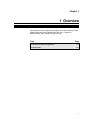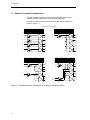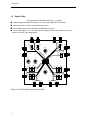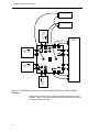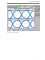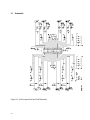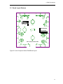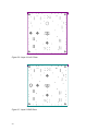
1
4x4 Crosspoint Switch EVM U s e r 's G u i d e User's Guide January 2004 HPL-D SLLU064A IMPORTANT NOTICE Texas Instruments Incorporated and its subsidiaries (TI) reserve the right to make corrections, modifications, enhancements, improvements, and other changes to its products and services at any time and to discontinue any product or service without notice. Customers should obtain the latest relevant information before placing orders and should verify that such information is current and complete. All products are sold subject to TI’s terms and conditions of sale supplied at the time of order acknowledgment. TI warrants performance of its hardware products to the specifications applicable at the time of sale in accordance with TI’s standard warranty. Testing and other quality control techniques are used to the extent TI deems necessary to support this warranty. Except where mandated by government requirements, testing of all parameters of each product is not necessarily performed. TI assumes no liability for applications assistance or customer product design. Customers are responsible for their products and applications using TI components. To minimize the risks associated with customer products and applications, customers should provide adequate design and operating safeguards. TI does not warrant or represent that any license, either express or implied, is granted under any TI patent right, copyright, mask work right, or other TI intellectual property right relating to any combination, machine, or process in which TI products or services are used. Information published by TI regarding third-party products or services does not constitute a license from TI to use such products or services or a warranty or endorsement thereof. Use of such information may require a license from a third party under the patents or other intellectual property of the third party, or a license from TI under the patents or other intellectual property of TI. Reproduction of information in TI data books or data sheets is permissible only if reproduction is without alteration and is accompanied by all associated warranties, conditions, limitations, and notices. Reproduction of this information with alteration is an unfair and deceptive business practice. TI is not responsible or liable for such altered documentation. Resale of TI products or services with statements different from or beyond the parameters stated by TI for that product or service voids all express and any implied warranties for the associated TI product or service and is an unfair and deceptive business practice. TI is not responsible or liable for any such statements. Following are URLs where you can obtain information on other Texas Instruments products and application solutions: Products Applications Amplifiers amplifier.ti.com Audio www.ti.com/audio Data Converters dataconverter.ti.com Automotive www.ti.com/automotive DSP dsp.ti.com Broadband www.ti.com/broadband Interface interface.ti.com Digital Control www.ti.com/digitalcontrol Logic logic.ti.com Military www.ti.com/military Power Mgmt power.ti.com Optical Networking www.ti.com/opticalnetwork Microcontrollers microcontroller.ti.com Security www.ti.com/security Telephony www.ti.com/telephony Video & Imaging www.ti.com/video Wireless www.ti.com/wireless Mailing Address: Texas Instruments Post Office Box 655303 Dallas, Texas 75265 Copyright 2003 - 2004, Texas Instruments Incorporated EVM IMPORTANT NOTICE Texas Instruments (TI) provides the enclosed product(s) under the following conditions: This evaluation kit being sold by TI is intended for use for ENGINEERING DEVELOPMENT OR EVALUATION PURPOSES ONLY and is not considered by TI to be fit for commercial use. As such, the goods being provided may not be complete in terms of required design–, marketing–, and/or manufacturing– related protective considerations, including product safety measures typically found in the end product incorporating the goods. As a prototype, this product does not fall within the scope of the European Union directive on electromagnetic compatibility and therefore may not meet the technical requirements of the directive. Should this evaluation kit not meet the specifications indicated in the EVM User’s Guide, the kit may be returned within 30 days from the date of delivery for a full refund. THE FOREGOING WARRANTY IS THE EXCLUSIVE WARRANTY MADE BY SELLER TO BUYER AND IS IN LIEU OF ALL OTHER WARRANTIES, EXPRESSED, IMPLIED, OR STATUTORY, INCLUDING ANY WARRANTY OF MERCHANTABILITY OR FITNESS FOR ANY PARTICULAR PURPOSE. The user assumes all responsibility and liability for proper and safe handling of the goods. Further, the user indemnifies TI from all claims arising from the handling or use of the goods. Please be aware that the products received may not be regulatory compliant or agency certified (FCC, UL, CE, etc.). Due to the open construction of the product, it is the user’s responsibility to take any and all appropriate precautions with regard to electrostatic discharge. EXCEPT TO THE EXTENT OF THE INDEMNITY SET FORTH ABOVE, NEITHER PARTY SHALL BE LIABLE TO THE OTHER FOR ANY INDIRECT, SPECIAL, INCIDENTAL, OR CONSEQUENTIAL DAMAGES. TI currently deals with a variety of customers for products, and therefore our arrangement with the user is not exclusive. TI assumes no liability for applications assistance, customer product design, software performance, or infringement of patents or services described herein. Please read the EVM User’s Guide and, specifically, the EVM Warnings and Restrictions notice in the EVM User’s Guide prior to handling the product. This notice contains important safety information about temperatures and voltages. For further safety concerns, please contact the TI application engineer. Persons handling the product must have electronics training and observe good laboratory practice standards. No license is granted under any patent right or other intellectual property right of TI covering or relating to any machine, process, or combination in which such TI products or services might be or are used. Mailing Address: Texas Instruments Post Office Box 655303 Dallas, Texas 75265 Copyright 2003 - 2004, Texas Instruments Incorporated www.ti.com 3 EVM WARNINGS AND RESTRICTIONS It is important to operate this EVM within the input voltage range of -0.7 V to 4 V and the output voltage range of -0.5 V to 4 V. Exceeding the specified input range may cause unexpected operation and/or irreversible damage to the EVM. If there are questions concerning the input range, please contact a TI field representative prior to connecting the input power. Applying loads outside of the specified output range may result in unintended operation and/or possible permanent damage to the EVM. Please consult the EVM User’s Guide prior to connecting any load to the EVM output. If there is uncertainty as to the load specification, please contact a TI field representative. During normal operation, some circuit components may have case temperatures greater than 60°C. The EVM is designed to operate properly with certain components above 60°C as long as the input and output ranges are maintained. These components include but are not limited to linear regulators, switching transistors, pass transistors, and current sense resistors. These types of devices can be identified using the EVM schematic located in the EVM User’s Guide. When placing measurement probes near these devices during operation, please be aware that these devices may be very warm to the touch. Mailing Address: Texas Instruments Post Office Box 655303 Dallas, Texas 75265 Copyright 2003 - 2004, Texas Instruments Incorporated Preface Read This First About This Manual This evaluation module (EVM) user’s guide describes the hardware, theory of operation, and use of the EVM for evaluating the high-speed performance and functionality of either the SN65LVDS125A or SN65LVDS250 4x4 crosspoint switches. How to Use This Manual Chapter 1 provides an overview of the functional configurations and signal paths. Typical hardware setup and results are discussed in Chapter 2. Chapter 3 provides schematics, the board layout, the board layers, fabrication notes, and bill of materials Related Documentation from Texas Instruments SN65LVDS125A, 4x4 1.5 Gbps LVDS Crosspoint Switch Data Sheet (SLLS595). SN65LVDS250, 4x4 2.5 Gbps LVDS Crosspoint Switch Data Sheet (SLLS594). If You Need Assistance www.ti.com E-mail technical support http://wwwk.ext.ti.com/sc/technical_support/email_tech_support.asp Product Information Centers: Americas (972) 644-5580 Australia 1-800-999-084 Belgium (English) +32 (0) 27 45 55 32 China 108-00-886-0015 Finland (English) +358 (0) 9 25173948 France +33 (0) 1 30 70 11 64 Germany +49 (0) 8161 80 33 11 Hong Kong 800-96-5941 Indonesia 001-803-8861-1006 Israel (English) 1800 949 0107 (free phone) Italy 800 79 11 37 (free phone) Japan 0120-81-0036 iii Korea 080-551-2804 Malaysia 1-800-80-3973 Netherlands (English) +31 (0) 546 87 95 45 New Zealand 0800-446-934 Phillippines 1-800-765-7404 Singapore 800-886-1028 Spain +34 902 35 40 28 Sweden (English) +46 (0) 8587 555 22 Taiwan 0800-006800 Thailand 001-800-886-0010 United Kingdom +44 (0) 1604 66 33 99 FCC Warning This equipment is intended for use in a laboratory test environment only. It generates, uses, and can radiate radio frequency energy and has not been tested for compliance with the limits of computing devices pursuant to subpart J of part 15 of FCC rules, which are designed to provide reasonable protection against radio frequency interference. Operation of this equipment in other environments may cause interference with radio communications, in which case the user at his expense will be required to take whatever measures may be required to correct this interference. If your book does not discuss a product that creates radio frequency interference, delete this section from your preface. If your book does discuss a product that creates radio frequency interference, you must include this warning as it appears above. iv Contents Read This First ................................................................................................................iii About This Manual..................................................................................................... iii How to Use This Manual ........................................................................................... iii Related Documentation from Texas Instruments ....................................................... iii If You Need Assistance ............................................................................................. iii FCC Warning............................................................................................................. iv Contents ........................................................................................................................... v Figures.............................................................................................................................. v Tables .............................................................................................................................. vi 1 Overview ....................................................................................................................1-1 1.1 Sample Functional Configurations ...................................................................1-2 1.2 Signal Paths ....................................................................................................1-4 2 Setup and Required Equipment ...............................................................................2-1 2.1 Applying an Input .............................................................................................2-1 2.2 Observing an Output........................................................................................2-4 2.3 Typical Test Results ........................................................................................2-4 3 EVM Construction .....................................................................................................3-1 3.1 Schematic........................................................................................................3-2 3.2 Board Layout Patterns .....................................................................................3-3 3.3 PCB Fabrication Requirements and Stack Up .................................................3-8 3.4 Bill of Materials ................................................................................................3-9 Figures Figure 1-1. Sample Functional Configurations of the 4x4 Crosspoint Switch ..........1-2 Figure 1-2. 4x4 Crosspoint Switch EVM ......................................................................1-3 Figure 1-3. 4x4 Crosspoint Switch Signal Paths.........................................................1-4 Figure 2-1. EVM Power Connections for Either SN65LVDS125A or SN65LVDS250 Evaluation. .............................................................................................................2-2 Figure 2-2. Termination for Interfacing LVDS, CML, or LVPECL Drivers ..................2-3 Figure 2-3. Typical Test Results...................................................................................2-5 Figure 3-1. 4x4 Crosspoint Switch EVM Schematic....................................................3-2 Figure 3-2. 4x4 Crosspoint Switch EVM Board Layout...............................................3-3 Figure 3-3. Layer 1–Signal Plane .................................................................................3-4 Figure 3-4. GND Plane...................................................................................................3-5 Figure 3-5. Layer 3–Vcc ................................................................................................3-5 v Tables Figure 3-6. Layer 4–Vcc01 Plane ..................................................................................3-6 Figure 3-7. Layer 5–GND Plane ....................................................................................3-6 Figure 3-8. Layer 6–GND/Signal Plane.........................................................................3-7 Tables Table 2-1 Crosspoint Function Table...........................................................................2-3 Table 3-2. Bill of Materials for the SN65LVDS125A / SN65LVDS250..........................3-9 vi Chapter 1 1 Overview This chapter provides a high-level description of the 4x4 crosspoint switch EVM mounted with either a SN65LVDS125A, 4x4 1.5-Gbps or a SN65LVDS250, 4x4 2.5-Gbps crosspoint switch. Topic Page 1.1 Sample Functional Configurations 1-2 1.2 Signal Paths 1-4 1-1 1 Overview 1.1 Sample Functional Configurations The 4x4 crosspoint switch is a fully non-blocking switch that provides flexibility in switch configuration for the desired application. A sample of various functions for which the EVMs can be configured is shown in Figure 1-1. C o n f ig u ra t i o n E x a m p l e s S10 0 S30 1 S11 0 S31 0 S20 0 S40 1 S21 1 S41 1 S10 0 S30 0 S11 0 S31 0 S21 0 S41 0 1A 1Y 1A 1Y 1B 1Z 1B 1Z 2A 2Y 2Y 2B 2Z 2Z 3A 3Y 3Y 3B 3Z 3Z 4A 4Y 4Y 4B 4Z 4Z S10 0 S30 1 S11 0 S31 0 S20 0 S40 1 S21 0 S41 0 S10 1 S30 0 S11 1 S31 0 S20 1 S40 0 S21 1 S41 0 1A 1Y 1A 1Y 1B 1Z 1B 1Z 2Y 2Y 2Z 2Z 3A 3Y 3Y 3B 3Z 3Z 4Y 4A 4Y 4Z 4B 4Z Figure 1-1. Sample Functional Configurations of the 4x4 Crosspoint Switch 1-2 S20 0 S40 0 1 Overview Figure 1-2 shows the 4x4 crosspoint switch EVM (part number SN65LVDS125A or SN65LVDS250). The EVM comes with either the SN65LVDS125A or SN65LVDS250 installed and a copy of the data sheet. The latest version of the data sheet is also available from www.ti.com. A/W # 6456526 A SN65LVDS125A SN65LVDS250 4X4 Crosspoint Switch EVM Figure 1-2. 4x4 Crosspoint Switch EVM 1-3 1 Overview 1.2 Signal Paths The signal paths on this EVM (see Figure 1-3) include: ❏ Sixteen edge-launch SMA connectors (J1–J16) for high-speed data transmission ❏ Eight jumpers (W1– W8) for active switch logic control ❏ Four jumpers (W9–W12) for enabling and disabling the outputs ❏ Three banana jacks (J17, J18, J19) for power and ground connections. Banana jack J20 is used for non-LVDS type configurations. J14 J15 J13 VCC 1DE VCC J10 3DE VCC 2DE W12 J11 J12 J19 W10 W11 VCC 4DE VCC01 J9 J16 J18 W9 J20 U1 GND J1 VCC S10 W1 1 VT ERM W2 W7 VCC S11 W8 VCC S40 J17 VCC S41 J8 W3 W4 VCC S20 W5 VCC VCC S21 VCC S30 J2 J3 J4 J5 ` Figure 1-3. 4x4 Crosspoint Switch Signal Paths 1-4 W6 VCC S31 J6 J7 Chapter 2 2 Setup and Required Equipment Both the SN65LVDS125A and the SN65LVDS250 LVDS driver output characteristics are compliant with the requirements of the TIA/EIA-644 standard. LVDS drivers nominally provide a 350-mV differential signal, with a 1.2-V offset from ground. These levels are attained when driving a 100-Ω differential line-termination test load. This requirement includes the effects of up to 32 standard receivers with their ground references offset up to ±1 V from that of the driver. This common-mode loading limitation of LVDS drivers affects how the driver’s characteristics are observed with this EVM, and the test setup that follows in this manual. By using three power jacks (J17, J18, and J19) and by optionally installing termination resistors, different methods of probing can be used to evaluate the device output characteristics. The typical setup for the 4x4 crosspoint switch EVM is shown in Figure 2-1. 2.1 Applying an Input While the use of a split power plane allows the EVM to be terminated within the oscilloscope, offsetting the EVM ground requires the inputs to the device to also be offset. Figure 2-1 shows how to offset the EVM and the inputs to the device. Setting power supply 1 to 3.3 V and power supply 2 to 1.2 V causes the voltage swing of the LVDS outputs to be within the limits of -200 mV to 200 mV instead of the typical 1 V to 1.4 V. This requires the inputs of the 4x4 crosspoint switch EVM to also be offset by 1.2 V, resulting in a voltage swing of -200 mV to 200 mV. VTERM, banana jack J20, is provided for non-LVDS input terminations such as LVPECL, which requires a termination voltage. When applying an LVDS input, VTERM can be left open or connected to GND, which is the common-mode voltage when using the aforementioned –200-mV to 200-mV input swing. 2-1 2 Setup and Required Equipment + 3.3V Power Supply #1 - + 1.2V Power Supply #2 - DATA, DATA Amplitude: 400 mV Offset: 0.0 V J15 J13 W11 U1 1 J19 VCC01 J17 VCC ` J14 VCC 2DE GND GND W12 J4 J12 J5 VCC 3D E GND J11 J10 J9 J8 J7 DATA, DATA Amplitude: 400 mV Offset: 0.0 V VCC W9 W10 GND W8 VCC S41 VCC S31 GND J6 W6 4DE GND W7 VCC S40 W5 GND DATA, DATA Amplitude: 400 mV Offset: 0.0 V VCC 1DE J 20 VCC S30 J18 W2 VCC S21 GND VTERM W1 VCC S11 W4 GND GND VCC S10 GND J3 W3 GND J16 J1 VCC S20 J2 GND DATA, DATA Amplitude: 400 mV Offset: 0.0 V SCOPE (internally terminated 50 Ω to GND) Figure 2-1. EVM Power Connections for Either SN65LVDS125A or SN65LVDS250 Evaluation. Many possible configurations for the 4x4 crosspoint switches are made available. Table 2-1 provides a description of the different functions and the required selector settings. 2-2 2 Setup and Required Equipment Table 2-1 Crosspoint Function Table Output Channel 1 Control Input Pins Selected Output Channel 2 Control Input Pins Selected Output Channel 3 Control Input Pins Selected Output Channel 4 Control Input Pins Selected S10 0 0 1 1 S20 0 0 1 1 S30 0 0 1 1 S40 0 0 1 1 S11 0 1 0 1 1Y/1Z 1A/1B 2A/2B 3A/3B 4A/4B S21 0 1 0 1 2Y/2Z 1A/1B 2A/2B 3A/3B 4A/4B S31 0 1 0 1 3Y/3Z 1A/1B 2A/2B 3A/3B 4A/4B S41 0 1 0 1 4Y/4Z 1A/1B 2A/2B 3A/3B 4A/4B Apply inputs to the SMA connectors J1–J8. The EVM comes with 50-Ω resistors installed to VTERM, providing a termination scheme easily adjusted to accommodate LVDS, LVPECL, or CML output structures. (See Figure 2-2). Vterm 50 Ω LVDS, LVPECL, or CML A SN65LVDS125 Input Channels 1-4 B 50 Ω Vterm Figure 2-2. Termination for Interfacing LVDS, CML, or LVPECL Drivers 2-3 2 Setup and Required Equipment 2.2 Observing an Output In order to minimize the parasitic capacitance in high-speed measurements (probe capacitance), the 4x4 crosspoint switch EVM provides an offset power plane (layer 5). This power plane allows the user to offset the device so that the common-mode output is compatible with the 50 ohms to ground termination within the scope. Terminating the EVM within the scope eliminates any bandwidth limitations introduced by a probe. Direct connection to an oscilloscope with 50-Ω internal terminations to ground is accomplished without requiring installation of resistors R5 – R16 on the EVM. The outputs are available at J9–J16 for direct connection to oscilloscope inputs. All cabling used to source and measure signals must be electrically matched in length to prevent any skew between conductors of the differential inputs. Referring back to 2-1, power supply 1 is used to provide the required 3.3 V to the EVM. Power supply 2 is used to offset the EVM ground relative to the device under test (DUT) ground. With this power scheme, the commonmode voltage seen by either the SN65LVDS125A or the SN65LVDS250 is approximately equal to that of the oscilloscope, thus preventing significant common-mode current flow. Using dual supplies and offsetting the EVM ground relative to the DUT ground are simply steps required for the test and evaluation of devices. Actual designs include high-impedance receivers, which do not require the setup steps outlined above. If the EVM outputs are to be evaluated with a high-impedance probe, direct probing on the EVM is supported via installation of a 100-Ω resistor across the solder pads (R5, R8, R11, and R14). Note: Power Supply 2 .Power supply 2 must be able to sink current. 2.3 Typical Test Results Figure 2-3 is a typical result obtained with the EVM setup shown in Figure 23 2-1. The inputs (J1–J8) were stimulated with a 2 –1 PRBS signal at 1.5 Gbps. The input levels for both clock and data were a differential voltage of 400 mV, with a common-mode voltage of 0 V (referenced to the ground of the pattern generator). 2-4 2 Setup and Required Equipment Figure 2-3. Typical Test Results. 2-5 2 Setup and Required Equipment 2-6 EVM Construction Chapter 3 3 EVM Construction This chapter presents the schematics, board layouts, fabrication information, and the bill of materials. Topic Page 3.1 Schematic 3-2 3.2 Board Layout Patterns 3-3 3.3 PCB Fabrication Requirements and Stack Up 3-8 3.4 Bill of Materials 3-9 3-1 SN65LVDS125A or SN65LVDS250 U1 3.1 Schematic Figure 3-1. 4x4 Crosspoint Switch EVM Schematic 3-2 3 EVM Construction 3.2 Board Layout Patterns A/W # 6456526 SN65LVDS125A SN65LVDS250 4X4 Crosspoint Switch EVM Figure 3-2. 4x4 Crosspoint Switch EVM Board Layout 3-3 Figure 3-3. Layer 1–Signal Plane 3-4 3 EVM Construction Figure 3-4. GND Plane Figure 3-5. Layer 3–Vcc 3-5 Figure 3-6. Layer 4–Vcc01 Plane Figure 3-7. Layer 5–GND Plane 3-6 3 EVM Construction Figure 3-8. Layer 6–GND/Signal Plane 3-7 3.3 PCB Fabrication Requirements and Stack Up Notes: 1. PWB TO BE FABRICATED TO MEET OR EXCEED IPC-6012, CLASS 3 STANDARDS AND WORKMANSHIP SHALL CONFORM TO IPC-A-600, CLASS 3 CURRENT REVISIONS 2. BOARD MATERIAL AND CONSTRUCTION TO BE UL APPROVED AND MARKED ON THE FINISHED BOARD. 3. LAMINATE MATERIAL:COPPER-CLAD NELCO N4000-13 (DO NOT USE -13SI) 4. COPPER WEIGHT: 1oz FINISHED 5. FINISHED THICKNESS: 0.062" +/- 0.010" 6. MIN PLATING THICKNESS IN THROUGH HOLES: .001" 7. SMOBC / HASL 8. LPI SOLDERMASK BOTH SIDES USING APPROPRIATE LAYER ARTWORK: COLOR = GREEN Stackup Signal: Layer 1 0.0075" GND: Layer 2 0.0075" VCC Power: Layer 3 0.062" 9. LPI SILKSCREEN AS REQUIRED: COLOR = WHITE 10. VENDOR INFORMATION TO BE INCORPORATED ON BACK SIDE WHENEVER POSSIBLE 11. MINIMUM COPPER CONDUCTOR WIDTH IS: 0.009" MINIMUM CONDUCTOR SPACING IS: 0.006" 12. NUMBER OF FINISHED LAYERS: 6 13. ALL 8 MIL HOLES TO BE PLUGGED AND COPLANAR TO SURFACE 14. SPACING BETWEEN LAYERS 1 AND 2 SHOULD BE 0.0075" SPACING BETWEEN LAYERS 2 AND 3 SHOULD BE 0.0075" SPACING BETWEEN LAYERS 4 AND 5 SHOULD BE 0.0075" SPACING BETWEEN LAYERS 5 AND 6 SHOULD BE 0.0075" 3-8 VCCO1 Power: Layer 4 0.0075" GND: Layer 5 0.0075" SIGNAL/GND: Layer 6 3 EVM Construction 3.4 Bill of Materials Table 3-2. Bill of Materials for SN65LVDS125A / SN65LVDS250 EVM Item 6456526-1 Qty 6456526-2 Qty 6456526-3 Qty Description Pattern Reference Designator 1 9 9 9 0.001 µF 402 C2, C3, C4, C5, C6, C7, C8, C9, C10 2 2 2 2 0.01 µF 603 C13, C18 3 1 1 1 0.1 µF 603 C21 4 2 2 2 0.1 µF 1206 C14, C19 5 4 4 4 100 Ω (uninstalled) 402 R5, R8, R11, R14 6 2 2 2 10 µF 7343 C11, C16 7 1 1 1 1 µF 603 C22 8 2 2 2 1 µF 1206 C15, C20 9 12 12 12 3 pos jumper 10 8 8 8 49.9 Ω (uninstalled) 402 R6, R7, R9, R10, R12, R13, R15, R16 11 8 8 8 49.9 Ω 402 R1, R2, R3, R4, R17, R18, R19, R20 12 2 2 2 68 µF Cap 592D R C12, C17 13 4 4 4 Banana jack 14 16 16 16 SMA PCB MT MOD 15 1 0 0 SN65LVDS125A 38-TSSOP (DBT) U1 16 0 1 0 SN65LVDS250 38-TSSOP (DBT) U1 17 0 0 1 Special 38-TSSOP (DBT) U1 18 4 4 4 Rubber feet 3/8” 19 1 1 1 PWB 6456526 W1, W2, W3, W4, W5, W6, W7, W8, W9, W10, W11, W12 J17, J18, J19, J20 SMA END 50 Ω J1, J2, J3, J4, J5, J6, J7, J8, J9, J10, J11, J12, J13, J14, J15, J16 PWB 3-9