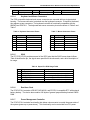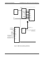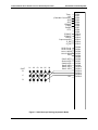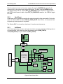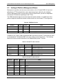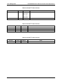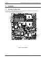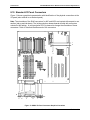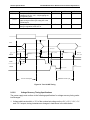
1
Intel® SHG2 DP Server Board Technical Product Specification Intel Order Number C11343-001 Revision 1.0 June 2002 Enterprise Platforms and Services Division Intel Order Number C11343-001 Revision History Intel® SHG2 DP Server Board Technical Product Specification Revision History Date 06/05/02 Revision Number 1.0 Modifications Final draft. Disclaimers Information in this document is provided in connection with Intel® products. No license, express or implied, by estoppels or otherwise, to any intellectual property rights is granted by this document. Except as provided in Intel's Terms and Conditions of Sale for such products, Intel assumes no liability whatsoever, and Intel disclaims any express or implied warranty, relating to sale and/or use of Intel products including liability or warranties relating to fitness for a particular purpose, merchantability, or infringement of any patent, copyright or other intellectual property right. Intel products are not intended for use in medical, life saving, or life sustaining applications. Intel may make changes to specifications and product descriptions at any time, without notice. ® The Intel SHG2 Server Board may contain design defects or errors known as errata that may cause the product to deviate from published specifications. Current characterized errata will be available on request. 2 I C is a two-wire communications bus/protocol developed by Philips. SMBus is a subset of the 2 2 I C bus/protocol and was developed by Intel Corporation. Implementations of the I C bus/protocol or the SMBus bus/protocol may require licenses from various entities, including Philips Electronics N.V. and North American Philips Corporation. ® Intel is a trademark or registered trademark of Intel Corporation or its subsidiaries in the United States and other countries. Copyright © Intel Corporation 2002. *Other names and brands may be claimed as the property of others. ii Intel Order Number C11343-001 Revision 1.0 Intel® SHG2 DP Server Board Technical Product Specification Table of Contents Table of Contents 1. Introduction............................................................................................................ 1 1.1 SHG2 Architecture Overview............................................................................... 2 1.2 Document Structure and Outline ......................................................................... 4 2. Processor and Chipset ......................................................................................... 6 2.1 Overview.............................................................................................................. 6 2.2 Processor Support............................................................................................... 6 2.2.1 Processor Bus Termination/Regulation/Power .............................................. 7 2.2.2 Miscellaneous Processor Subsystem Logic................................................... 7 2.2.3 Server Management Registers and Sensors ................................................. 7 2.2.4 ServerWorks* Grand Champion* LE Chipset ................................................ 8 2.2.5 CMIC-LE .................................................................................................... 8 2.3 Memory Subsystem............................................................................................. 9 2.3.1 Chipkill* .......................................................................................................... 9 2.3.2 Memory Configuration.................................................................................... 9 2.3.3 CIOB-X2 ................................................................................................... 11 2.4 CSB5 South Bridge ........................................................................................... 11 2.4.1 PCI Interface................................................................................................ 12 2.4.2 PCI Bus Master IDE Interface...................................................................... 12 2.4.3 USB Interface .............................................................................................. 12 2.4.4 BIOS Flash .................................................................................................. 12 2.4.5 Compatibility Interrupt Control ..................................................................... 12 2.4.6 Power Management ........................................................................................ 13 2.4.7 General Purpose Input and Output Pins ...................................................... 13 Revision 1.0 Intel Order Number C11343-001 iii Table of Contents 2.5 Intel® SHG2 DP Server Board Technical Product Specification Chipset Support Components ........................................................................... 14 2.5.1 Legacy I/O (Super I/O) National* PC87417VLA........................................... 14 3. Baseboard PCI I/O Subsystem ........................................................................... 18 3.1 Overview............................................................................................................ 18 3.2 64-bit/100MHz PCI-X Subsystem ...................................................................... 18 3.2.1 Device IDs (IDSEL)...................................................................................... 18 3.2.2 64/100MHz PCI-X Arbitration....................................................................... 19 3.2.3 82544GC Gigabit Ethernet Controller .......................................................... 19 3.3 64-bit/133MHz PCI-X Subsystem ...................................................................... 19 3.3.1 Device IDs (IDSEL)...................................................................................... 19 3.3.2 64/133MHz Segment Arbitration.................................................................. 19 3.3.3 Ultra 160 SCSI Controller (Adaptec* AIC- 7899) ......................................... 20 3.4 Modular RAID Capable PCI Slot 6 .................................................................... 20 3.5 32-bit/33-MHz PCI Subsystem .......................................................................... 20 3.5.1 Device IDs (IDSEL)...................................................................................... 21 3.5.2 32/33 MHz PCI Arbitration ........................................................................... 21 3.5.3 Network Interface Controller (NIC)............................................................... 21 3.5.4 Video Controller ........................................................................................... 22 3.6 Interrupt Routing................................................................................................ 23 3.6.1 Serialized IRQ support................................................................................. 26 3.6.2 IRQ scan for PCIIRQ ................................................................................... 26 4. Clock Generation and Distribution .................................................................... 27 5. Server Management ............................................................................................ 29 iv 5.1 Sahalee Baseboard Management Controller .................................................... 30 5.2 System Reset Control........................................................................................ 31 Intel Order Number C11343-001 Revision 1.0 Intel® SHG2 DP Server Board Technical Product Specification Table of Contents 5.2.1 Power-up Reset ........................................................................................... 31 5.2.2 Hard Reset................................................................................................... 32 5.2.3 Soft Reset .................................................................................................... 32 5.3 Intelligent Platform Management Buses............................................................ 33 6. Error Reporting and Handling ............................................................................ 35 6.1 Error Sources and Types................................................................................... 35 6.2 Handling and Logging System Errors ................................................................ 35 6.2.1 6.3 Logging Format Conventions ....................................................................... 35 System Management Interrupt (SMI) Handler ................................................... 37 6.3.1 PCI Bus Error............................................................................................... 37 6.3.2 Intel Xeon Processor Bus Error .............................................................. 37 6.3.3 Memory Bus Error........................................................................................ 37 6.3.4 System Limit Error ....................................................................................... 37 6.3.5 Processor Failure......................................................................................... 37 6.3.6 Boot Event ................................................................................................... 38 6.3.7 Chip Set Failure ........................................................................................... 38 6.4 Firmware (BMC) ................................................................................................ 38 6.4.1 System Event Log (SEL) Full....................................................................... 38 6.4.2 Timestamp Clock ......................................................................................... 38 6.4.3 Fault Resilient Booting ................................................................................. 38 6.5 Error Messages and Error Codes ...................................................................... 39 6.5.1 Alert Standard Forum (ASF) Progress Codes.............................................. 40 6.5.2 Power-On Self Test (POST) Codes ............................................................. 40 6.5.3 POST Error Codes and Messages .............................................................. 44 6.5.4 Liquid Crystal Display (LCD) ........................................................................ 46 Revision 1.0 Intel Order Number C11343-001 v Table of Contents Intel® SHG2 DP Server Board Technical Product Specification 7. Jumpers ............................................................................................................... 48 7.1 Hardware Configuration..................................................................................... 48 8. Connections......................................................................................................... 50 8.1 Connector Locations ......................................................................................... 50 8.2 Power Distribution Board Interface Connector .................................................. 51 8.3 SCSI Connectors............................................................................................... 52 8.4 Floppy Connector .............................................................................................. 53 8.5 IDE Connectors ................................................................................................. 54 8.6 Front Panel Interface......................................................................................... 55 8.7 Processor Connector......................................................................................... 56 8.8 System Management Interfaces........................................................................ 60 8.8.1 ICMB Connector .......................................................................................... 60 8.8.2 Auxiliary I2C* Connector .............................................................................. 60 8.9 Baseboard Fan Connectors............................................................................... 61 8.9.1 8.10 Fan Connector Pin-out................................................................................. 63 Standard I/O Panel Connectors...................................................................... 64 8.10.1 Universal Serial Bus (USB) Interface ......................................................... 65 8.10.2 Mouse and Keyboard Ports ....................................................................... 66 8.10.3 Serial Ports ................................................................................................ 66 8.10.4 Parallel Port ............................................................................................... 67 8.10.5 Video Port .................................................................................................. 68 8.10.6 Ethernet Connectors .................................................................................. 68 8.11 Connector Manufacturers and Part Numbers................................................. 70 9. General Specifications........................................................................................ 72 9.1 vi Absolute Maximum Electrical and Thermal Ratings .......................................... 72 Intel Order Number C11343-001 Revision 1.0 Intel® SHG2 DP Server Board Technical Product Specification Table of Contents 9.2 Airflow Specification for CIOB-X2 and CMIC-LE ............................................... 73 9.3 Electrical Specifications..................................................................................... 73 9.3.1 Power Consumption..................................................................................... 73 9.3.2 Power Supply Specifications........................................................................ 74 10. Mechanical Specifications.................................................................................. 78 11. Regulatory and Integration Information ............................................................ 80 11.1 Product Regulatory Compliance..................................................................... 80 11.1.1 Product Safety Compliance ....................................................................... 80 11.1.2 Product EMC Compliance.......................................................................... 80 11.1.3 Product Regulatory Compliance Markings................................................. 80 11.2 Electromagnetic Compatibility Notices ........................................................... 80 11.2.1 Europe (CE Declaration of Conformity) ..................................................... 80 11.2.2 Australian Communications Authority (ACA) (C-Tick Declaration of Conformity).............................................................................................................. 81 11.2.3 Ministry of Economic Development (New Zealand) Declaration of Conformity ............................................................................................................... 81 11.2.4 11.3 BSMI (Taiwan) ........................................................................................... 81 Replacing the Back up Battery ....................................................................... 81 Appendix A: Glossary .................................................................................................. I Appendix B: Reference Documents.......................................................................... III Revision 1.0 Intel Order Number C11343-001 vii List of Figures Intel® SHG2 DP Server Board Technical Product Specification List of Figures Figure 1. Intel® SHG2 Server Board ............................................................................... 1 Figure 2. SHG2 Server Board Placement Diagram ........................................................ 2 Figure 3. SHG2 Memory Bank Layout.......................................................................... 10 Figure 4. SHG2 Interrupt Routing (PIC Mode).............................................................. 24 Figure 5. SHG2 Interrupt Routing (Symmetric Mode)................................................... 25 Figure 6. SHG2 Baseboard Clock Distribution ............................................................. 28 Figure 7. SHG2 Sahalee BMC Block Diagram ............................................................. 29 Figure 8. Basic Reset Flow........................................................................................... 32 Figure 9. Jumper Location............................................................................................. 48 Figure 10. SHG2 Baseboard Connector Identification and Locations ........................... 50 Figure 11. SHG2 Board Fan Connector Locations ........................................................ 61 Figure 12. SHG2 System Redundant Cooling Fan Support .......................................... 62 Figure 13. SHG2 I/O Panel Connector Graphical Locations ......................................... 64 Figure 14. SHG2 I/O Panel Connector Location Dimensions........................................ 69 Figure 15. Output Voltage Timing.................................................................................. 75 Figure 16. Turn On/Off Timing ...................................................................................... 76 Figure 17. SHG2 Baseboard Mechanical Diagram 1..................................................... 78 Figure 18. SHG2 Baseboard Mechanical Diagram 2..................................................... 79 viii Intel Order Number C11343-001 Revision 1.0 Intel® SHG2 DP Server Board Technical Product Specification List of Tables List of Tables Table 1. Memory DIMM Pairs....................................................................................... 10 Table 2. CSB5 GPIO Usage Table............................................................................... 13 Table 3. Serial Port Connector Pinout .......................................................................... 14 Table 4. Parallel Port Connector Pinout ....................................................................... 15 Table 5. Floppy Port Connector Pinout ........................................................................ 15 Table 6. Keyboard Connector Pinout ........................................................................... 16 Table 7. Mouse Connector Pinout ................................................................................ 16 Table 8. Super I/O* GPIO Usage Table ....................................................................... 16 Table 9. PCI(-X) Bus Segment Characteristics ............................................................ 18 Table 10. 64/100MHz Segment Configuration IDs ........................................................ 18 Table 11. 64/100MHz Segment Arbitration Connections .............................................. 19 Table 12. 64/133MHz Segment Configuration IDs ........................................................ 19 Table 13. 64/133 MHz Segment Arbitration Connections ............................................. 20 Table 14. 32/33MHz Segment Configuration IDs .......................................................... 21 Table 15. 32/33MHz Segment Arbitration Connections ................................................ 21 Table 16. Standard VGA Modes ................................................................................... 22 Table 17. Video Port Connector Pinout ......................................................................... 23 Table 18. ADM1026* Input Definition ............................................................................ 30 Table 19. Temperature Sensors.................................................................................... 31 Table 20: IPMB Bus Devices........................................................................................ 33 Table 21. Private I2C* Bus 1 Devices ............................................................................ 33 2 Table 22: Private I C* Bus 2 Devices ............................................................................ 33 Table 23: Private I2C* Bus 3 Devices ............................................................................ 34 2 Table 24: Private I C* Bus 4 Devices ............................................................................ 34 2 Table 25: Private I C* Bus 5 Devices ............................................................................ 34 Table 26. BIOS Logging SEL List.................................................................................. 36 Table 27. Event Request Message Event Data Field Contents..................................... 36 Table 28. Event Request Message Event Data Field Contents..................................... 40 Table 29. Port-80h Code Definition ............................................................................... 40 Table 30. Standard BIOS POST Codes ........................................................................ 41 Revision 1.0 Intel Order Number C11343-001 ix List of Tables Intel® SHG2 DP Server Board Technical Product Specification Table 31. Recovery BIOS POST Codes........................................................................ 44 Table 32. POST Error Messages and Codes ................................................................ 45 Table 33. SHG2 Configuration Jumper Options ............................................................ 49 Table 34. SHG2 Baseboard Connectors ....................................................................... 50 Table 35. Main Power Connector .................................................................................. 51 Table 36. +12V Power Connector ................................................................................. 51 2 Table 37. Power Connector for I C* Bus ....................................................................... 52 Table 38. 68-pin SCSI Connector Pin-out ..................................................................... 52 Table 39. Legacy 34-pin Floppy Connector Pin-out ...................................................... 53 Table 40. Primary/Secondary IDE 40-pin Connector Pinout ......................................... 54 Table 41. AT Front Panel Header Pinout ...................................................................... 55 Table 42. Intel® Xeon™ Processor Connector Pinout ................................................... 56 Table 43. ICMB Connector Pin-out................................................................................ 60 Table 44. IPMB Connector Pinout ................................................................................. 60 Table 45. SC5200 Fan Implementation........................................................................ 63 Table 46. Fan Connector Pinout ................................................................................... 63 Table 47. I/O Panel Connectors .................................................................................... 65 Table 48. USB Connector ............................................................................................. 65 Table 49. Internal USB Connector................................................................................. 65 Table 50. Mouse and Keyboard Ports ........................................................................... 66 Table 51. Serial A Port Connector................................................................................. 66 Table 52. Serial B Port Header: COM2/EMP ................................................................ 67 Table 53. Parallel Port Connector ................................................................................. 67 Table 54. Video Connector............................................................................................ 68 Table 55. Ethernet Connectors ..................................................................................... 68 Table 56. LAN1 10/100 LED Schemes ......................................................................... 69 Table 57. LAN2 10/100/1000 LED Schemes ................................................................ 69 Table 58. Baseboard Connector Manufacturer Part Numbers ...................................... 70 Table 59. Absolute Maximum Electrical and Thermal Specifications ............................ 72 Table 60. Thermal Specification for Key Components .................................................. 72 Table 61. Airflow Specification for Key Components..................................................... 73 Table 62. SHG2 Power Budget ..................................................................................... 73 Table 63. SHG2 DC Power Supply Voltage Specification ............................................. 74 x Intel Order Number C11343-001 Revision 1.0 Intel® SHG2 DP Server Board Technical Product Specification List of Tables Table 64. SHG2 Ripple and Noise Specification ........................................................... 74 Table 65. Voltage Timing Parameters ........................................................................... 74 Table 66. Turn On/Off Timing........................................................................................ 75 Table 67. Transient Load Requirements ....................................................................... 77 Revision 1.0 Intel Order Number C11343-001 xi List of Tables Intel® SHG2 DP Server Board Technical Product Specification < This page intentionally left blank. > xii Intel Order Number C11343-001 Revision 1.0 Intel® SHG2 DP Server Board Technical Product Specification 1. Introduction Introduction ® This chapter provides an architectural overview of the Intel SHG2 Server Board, including functional blocks and the electrical relationships. Figure 1 shows the functional blocks of the SHG2 baseboard. D IM M P re s to n ia P ro c e s s or 4 00M T /s 100MHz 4x FSB C M IC -L E 2 00M T /s 100MHz 2x D IM M D D R 200 C H A D IM M 2 00M T /s 100MHz 2x D IM M D D R 20 0 C H B P re s to n ia P ro c es s o r D IM M D IM M Thin IM B 4 00 M T /s 2 00 M H z 2x 1 2G B D D R 2 0 0 E C C M em o ry (6 D IM M s ) 2 -w a y inte rle av ed 8 00 M T /s 400MHz 2x R ear USB U S B 1 .1 Rear USB U S B 1 .1 R ear USB U S B 1 .1 IM B ATA 100 PCI 32/33 CSB5 IDE U S B 1.1 IDE F ro n t Panel USB A T A 10 0 PCI-X 133 PCI 32 LPC F la s h PCI 32 PCI-X 100 X BUS C IO B X 2 M R O M B E na b le d PC I 64 BM C PCI 32 PCI 64 PC I 64 V id e o L AN 10 /1 0 0 V ide o Conn U 1 60 / U 3 20 SCSI S IO R J 45 S e ria l P o rts P S /2 P a ra llel F lo p p y Int SCSI Conn In t SCSI Conn G b it L AN RJ45 ® Figure 1. Intel SHG2 Server Board Revision 1.0 Intel Order Number C11343-001 1 Introduction Intel® SHG2 DP Server Board Technical Product Specification +12V CPU Pwr 1 23 4 USB 1 1 8 8 5 2 1 C 6 B A 2 1 5 3 6 36 DIMM 3B Serial A Proc 1 DIMM 3A DIMM 2B 1 1 5 50 5 9 Parallel Aux Sig 1 KB/MS Main Pwr DIMM 2A DIMM 1B DIMM 1A 2 1 1 16 1 1 4 1 Video NIC2 (Gbit) Proc 2 82 71 NIC1 (10/100) Video 7 CMIC-LE Gbit Serial B PCIX-1 (64/100) Floppy USB BMC PCIX-2 (64/100) 2 1 1 Sec IDE 4 2 0 0 2 1 1 Prim IDE 4 2 0 0 Front Panel PCI-3 (32/33) 10/100 NIC SCSI CIOB-X2 PCI-4 (32/33) SIO CSB5 PCI-5 (32/33) LVD SCSI B LVD SCSI A 3 3 6 5 2 1 PCIX-6 (64/133) 6 6 8 3 7 3 4 3 3 3 6 5 2 1 6 6 8 3 7 3 4 3 Figure 2. SHG2 Server Board Placement Diagram 1.1 SHG2 Architecture Overview The Intel® SHG2 Server Board is designed around the Intel® Xeon™ processor and the ServerWorks* Grand Champion* LE ServerSet* chipset. This combination provides the basis for a high performance system with leading edge processor, memory, and I/O performance. The SHG2 baseboard architecture provides for two INT3-compliant (603 pin) processor sockets supporting dual processing operation using Intel Xeon processors. It also contains six industry standard PCI and PCI-X expansion slots supporting a mixture of 32-bit/33-MHz, 64-bit/100-MHz and 64-bit/133-MHz slots. The processor baseboard provides an array of embedded I/O devices including a SCSI controller that provides two independent channels at SCSI bus speeds up to 160MB/sec with 7899 SCSI controller, one embedded 10/100 Network Interface Controller (NIC), one 10/100/1000 Gigabit Network Interface Controller, and a 2D/3D graphics accelerator. 2 Intel Order Number C11343-001 Revision 1.0 Intel® SHG2 DP Server Board Technical Product Specification Introduction Server management and monitoring hardware are also included. These features, and the others listed below, make this one of the most highly integrated server boards in this class. SHG2 supports two interleaved memory channels at 100 MHz, each utilizing the rising edge and falling edge of the clock cycle for 200MT/s per channel (also known as “double pumped”) for a combined throughput of 400 MT/s. The subsystem was originally intended for PC1600 DDR memory modules (DDR200), however up to 6 DDR200 of DDR266 registered memory modules (PC1600 or PC2100 DIMMs) inserted as pairs may be used. Each DIMM may provide up to 2 GB of memory capacity, providing up to 12 GB of system memory. Note: Although the use of DDR266 modules is supported for upward compatibility, the channel throughput is fixed at 400 MT/s, and the use of higher speed DIMMs will not provide additional bandwidth. Mixed memory is not recommended, all DIMM sites should be populated with the same speed and, when possible, same manufacturer. The SHG2 server board provides the following features: • • • • • • • • Dual Intel Xeon processor support. - Two processor sockets for installation of one to two identical Intel Xeon processors. - Embedded VRMs to support two Xeon processors. ServerWorks Grand Champion LE chipset. - Champion Memory and I/O Controller-Low End (CMIC-LE). - Champion South Bridge (CSB5). - Champion I/O Bridge (CIOBX2). Support for 6 DDR registered ECC Synchronous Dynamic RAM (SDRAM) DIMMs. - Error Correcting Code (ECC) single-bit correction, and multiple-bit error detection and memory scrubbing. - Supports Chipkill* technology 32-bit, 33-MHz 5V keyed PCI segment with three expansion connectors and two embedded devices with external connectors. - One PCI NIC—Intel 82550PM Fast Ethernet Controller with a dedicated RJ-45 connector at the rear I/O panel - 3D/2D Graphics Accelerator —ATI* RAGE XL Video Controller with DB15 VGA connector at the rear I/O panel 64-bit, 100-MHz, 3.3V PCI-X segment with two expansion connectors and one embedded device. - One PCI-X network interface controller—Intel 82544GC Gigabit Ethernet Controller with a dedicated RJ-45 connector at the rear I/O panel 64-bit, 133-MHz, 3.3V PCI-X segment with one expansion connector and one embedded device. - Dual Channel Ultra* 160 SCSI Controller—Adaptec* 7899 SCSI Controller. Note: When the 7899 SCSI Controller is enabled, this bus segment will run at 66MHz in PCI mode. When disabled, the segment is capable of 133MHz PCI-X mode. X-bus segment with one embedded device. - 8-Mbit flash device for system BIOS. LPC bus segment with two embedded devices. Revision 1.0 Intel Order Number C11343-001 3 Introduction Intel® SHG2 DP Server Board Technical Product Specification Super I/O* controller chip providing all PC-compatible I/O (floppy, parallel, serial, keyboard, mouse). - Sahalee Baseboard Management Controller (BMC) providing monitoring, alerting, and logging of critical system information obtained from embedded sensors on baseboard. Four Universal Serial Bus (USB) ports. Two 68 pin Ultra SCSI connectors, supporting two SCSI U-160 channels Two 40 pin fast ATA (IDE) connectors, supporting two ATA 33/66/100 channels - • • • 1.2 Document Structure and Outline The information contained in this document is organized into 11 chapters. The content of each chapter is summarized below: Chapter 1: Introduction Architectural overview of the Intel SHG2 Server Board showing functional blocks and identifying major features. Chapter 2: Processor and Chipset Detailed description of the chipset and the supported processors. Chapter 3: Baseboard PCI I/O Subsystem Detailed descriptions of the PCI I/O subsystem. Three PCI buses are detailed, with specifics on embedded devices and provided slots. Interrupt routing information is also provided. Chapter 4: Clock Generation and Distribution Identification of the clock signals generated and used on the SHG2 server board, and detailed drawings of their implementation. Chapter 5: Server Management Detailed description of the server management hardware integrated on the SHG2 baseboard. I2C* addresses and block diagrams are provided. Chapter 6: Error Handling and Reporting Defines how errors are handled by the system BIOS and SHG2 server board. Chapter 7: Jumpers Identification and description of all jumpers used on the SHG2 server board. Chapter 8: Connections Identification of all connectors on the SHG2 server board, by ‘CN’ number and manufacturer's part number. Interfacing specifics are identified where applicable. Chapter 9: General Specifications Description of operational parameters and considerations, and other hardware specifications. Chapter 10: Mechanical Specifications Mechanical drawings of the Intel SHG2 Server Board. 4 Intel Order Number C11343-001 Revision 1.0 Intel® SHG2 DP Server Board Technical Product Specification Chapter 11 Revision 1.0 Introduction Regulatory and Integration Information Intel Order Number C11343-001 5 Processor and Chipset Intel® SHG2 DP Server Board Technical Product Specification 2. Processor and Chipset 2.1 Overview The Intel SHG2 Server Board consists of one to two identical Intel Xeon processors, the Grand Champion LE chipset, and support circuitry. The baseboard houses two surface mount zero insertion force (ZIF) processor sockets and one embedded processor voltage regulator module (VRMs) to power one or both processors. The ServerWorks* Grand Champion LE chipset provides the 36-bit address/64-bit data processor host bus interface, operating at 100 MHz in the AGTL+ signaling environment. The Grand Champion Memory and I/O Controller (CMIC-LE) provides an integrated memory controller, a high-speed I/O connection (IMB) to the PCI-X bridge (CIOB-X2) and a connection (Thin IMB) to the south bridge (CSB5) for legacy devices and the PCI segment. The server board supports up to 12 GB of ECC memory, using 2GB DDR-registered PC1600 or PC2100 SDRAM DIMMs. Additional descriptions and features include the following: • • • • • 2.2 ServerWorks Grand Champion LE chipset providing an integrated I/O bridge and memory controller, and a flexible I/O subsystem core (PCI) optimized for multiprocessor systems and standard high-volume (SHV) servers. Dual (603 pin) processor sockets that accept the Intel Xeon processors. Processor host bus AGTL+ supported circuitry, including termination power supply. Integrated APIC signals support. Miscellaneous logic for reset configuration, processor presence detection, ITP port, and server management. Processor Support SHG2 specifically supports Intel Xeon processors from 1.8 GHz to 2.6 GHz, with 512 KB of L2 advanced transfer cache. The processor is packaged in a 603-pin micro- Pin-Grid Array (PGA) and provides an integrated heat spreader (IHS) for heat sink attachment. The Intel Xeon processor socket that conforms to the 603-pin Socket Design Guidelines is a surface mount technology (SMT); ZIF socket using soldered ball attachment (BGA) to the platform. ® ® As with previous versions of Intel Pentium Pro processors, the Intel Xeon processor external interface is designed to be DP-ready. Each processor contains a local advanced programmable interrupt controller (APIC) section for interrupt handling. When two processors are installed, both processors must be of identical revision, core voltage, cache voltage, and bus/core speeds. Note: When using only one processor in the system, install the processor into the primary socket (PROC1, closest to the corner of the board). This will enable on-die termination on the end-agent processor the for system to function properly. The BMC will not allow DC power to 6 Intel Order Number C11343-001 Revision 1.0 Intel® SHG2 DP Server Board Technical Product Specification Processor and Chipset be applied to the system unless primary slot is populated with a processor, unless used in fault resilient booting (FRB) mode (details in Section 5). When using two processors, notice that the processor pins are physically 180 degrees out-ofphase. Improper processor installation may permanently damage processor pins. 2.2.1 Processor Bus Termination/Regulation/Power The termination circuitry required by the Intel Xeon processor bus (AGTL+) signaling environment, and the circuitry to set the AGTL+ reference voltage, are implemented directly on the processors. The baseboard provides 1.5 V AGTL+ termination power (VTT), and VRM 9.1compliant DC-to-DC converters to provide processor power (VCC_P) at each socket. The baseboard provides two embedded VRMs to power the processors, which derive power from the +5 V and 12 V supplies. Both processors share the same VRM to power their core. 2.2.2 Miscellaneous Processor Subsystem Logic In addition to the circuitry described above, the processor subsystem contains the following: • • • Reset configuration logic. Processor presence detection circuitry. Server management registers and sensors. 2.2.2.1 Reset Configuration Logic On the SHG2 platform, the BMC is responsible for configuring the processor speeds. The BMC uses the processor speed information (derived from the Intel Xeon processor SECC FRU 2 devices) to determine the appropriate speed to program into the speed-setting device (I Cbased EEPROM Mux). The processor information is read at every system power-on. The EEMUX is set to correspond to the speed of the slowest processor. 2.2.2.2 Processor Presence Detection Logic is provided on the baseboard to detect the presence and identity a properly installed processor. This prevents system power on if an empty socket in the primary section is detected in the primary processor socket (labeled Proc1, located closest to the edge of the server board), thus preventing operation of the system with an improperly terminated AGTL+ processor bus. The BMC checks this logic and will not turn on the system DC power until the bus is terminated properly with a processor in the primary socket. 2.2.2.3 APIC Bus Interrupt notification and generation for the processors is done using a front side bus (FSB) between local APIC, in each processor, and the I/O APIC in the CSB5 located on the baseboard. 2.2.3 Server Management Registers and Sensors The BMC manages registers and sensors associated with the processor/memory subsystem. Revision 1.0 Intel Order Number C11343-001 7 Processor and Chipset 2.2.4 Intel® SHG2 DP Server Board Technical Product Specification ServerWorks* Grand Champion* LE Chipset The CMIC-LE, CIOB-X2, and CSB5 chips provide the pathway between processor and I/O systems. The CMIC-LE is responsible for accepting access requests from the host (processor) bus, and directing all I/O accesses to one of the PCI buses or legacy I/O locations. If the cycle is directed to one of the 64-bit PCI segments, the CMIC-LE communicates with the CIOB-X2 through a private interface called the IMB bus. If the cycle is directed to the 32-bit PCI segment or to the CSB5, the cycle is output on the private interface between the CMIC-LE and the CSB5 called the Thin-IMB bus. The CIOB-X2 translates the IMB bus operation to a 64-bit PCI-X signaling environment, operating at 100 MHz or 133 MHz (PCI Local Bus Specification 2.2 and PCI-X Specification 1.0a compliant). The IMB bus consists of two data paths, one upstream (to the CMIC-LE from the CIOB-X2) and one downstream (from the CMIC-LE to the CIOB-X2). The interface is 16 bits wide and operates at 400 MHz with double-pumped data, providing over 1.6 GB per second of bandwidth in each direction, or 3.2 GB per second of bandwidth in both directions concurrently. All I/O for the SHG2 server board, including PCI-X, is directed through the CMIC-LE and then through either the CIOB-X2 or the CSB5-provided 32-bit/33-MHz PCI bus. • • The CSB5 provides a 32-bit/33-MHz PCI bus. The CIOB-X2 provides a 64-bit/100-MHz PCI-X bus and the 64-bit/133-MHz PCI-X bus. This independent bus structure allows all three PCI buses to operate concurrently and provides 1.2 GB per second of I/O bandwidth. 2.2.5 CMIC-LE The Champion Memory and I/O Controller (CMIC-LE) is the fourth generation product in ServerWorks* Champion ServerSet Technology. The CMIC-LE is built on top of the proven components of previous generations like the Intel® Pentium® Pro Bus interface unit, the IMB interface unit, and the DDR SDRAM memory interface unit. The CMIC-LE integrates two main functional units: 1) an integrated high performance main memory subsystem, and 2) an IMB bus interface that provides a high-performance data flow path between the processor bus and the I/O subsystem. In addition to the above-mentioned units, the CMIC-LE incorporates a Thin-Intra Module Bus (Thin-IMB) Interface. Other features provided by the CMIC-LE include the following: • • • • • • • 8 Full support of processor bus protocol with multiprocessor support. Full support of ECC on the memory interface. An in-order queue (twelve deep). Full support of registered DDR ECC SDRAM DIMMs. Addressing support for 12 GB of 2-way interleaved SDRAM with 6 DIMMs sockets. Memory scrubbing. Multiple-bit error detection and Multiple-bit error correction for 1-4 bits on one DRAM within the same DIMM module (Chipkill*). Intel Order Number C11343-001 Revision 1.0 Intel® SHG2 DP Server Board Technical Product Specification 2.3 Processor and Chipset Memory Subsystem Features provided in the SHG2 server board memory subsystem include the following: • • • • • • • • • • Six DIMM sockets, supporting three pairs of PC1600 (DDR200), upward compatible with PC2100 (DDR266) DIMMs. Memory can be implemented with either single-sided (one row) or double-sided (two row) DIMMs. Minimum memory capacity of 256 MB (2 x 128MB DIMMs). Maximum memory capacity of 12 GB (6 x 2GB DIMMs). The DIMM organization is x72, which includes 8 ECC check bits. Supports memory scrubbing, ECC single bit error correction, and multiple bit error detection. ECC from the DIMMs is passed through to the processor FSB. Supports Chipkill* multiple bit error detection and multiple bit error correction. Support for 2-way interleaved DDR SDRAM. The DDR SDRAM interface is comprised of 2 channels running at a frequency of 200 MHz each for for a total interleaved transfer rate of 400MT /s. Note: Memory interleaving is a way to increase memory performance by allowing the system to access multiple memory modules simultaneously, rather than sequentially, in a similar fashion to hard-drive striping. Interleaving can only take place between identical memory modules. Note: Although the use of DDR266 modules is supported for upward compatibility, the channel throughput is fixed at 400 MT/s, and the use of higher speed DIMMs will not provide additional bandwidth. Mixed memory is not recommended, all DIMM sites should be populated with the same speed and, when possible, same manufacturer. 2.3.1 Chipkill* The CMIC-LE chipset supports Chipkill memory technology, which allows the system to recover when a multi-bit error is encountered within a single DDR SDRAM device on the same DIMM module. Chipkill memory technology provides protection up to, and including, a complete failure of a single DRAM device. The Chipkill technology incorporated in the CMIC-LE does not require any layout requirements on the memory boards. CMIC-LE contains the Chipkill algorithm and performs all the data correction logic required. Chipkill memory technology works by re-ordering the data from the DDR SDRAMs so that if one DDR SDRAM device within a module should fail, the check bit algorithm provides sufficient information to recover from the multi-bit data error. The correctable errors are then written to the system error log (SEL) for evaluation at a later time. 2.3.2 Memory Configuration Memory configuration requirements are as follows: • • • DDR200 or DDR266 SDRAM-registered DIMM modules DIMM organization: x72 ECC Pin count: 184 Revision 1.0 Intel Order Number C11343-001 9 Processor and Chipset • • • • Intel® SHG2 DP Server Board Technical Product Specification DIMM capacity (in pairs): 128 MB, 256 MB, 512 MB, 1 GB and 2 GB Serial PD: JEDEC Rev 2.0 Voltage Options: 2.5 V (VDD/VDDQ) DIMMs must be populated in pairs for a x144 wide memory data path Table 1. Memory DIMM Pairs Memory DIMM DIMM PAIR Row DIMM 1A, DIMM 1B 1 1, 2 DIMM 2A, DIMM 2B 2 3, 4 DIMM 3A, DIMM 3B 3 5, 6 DIMM Pair 3A/B DIMM Pair 2A/B DIMM Pair 1A/B Figure 3. SHG2 Memory Bank Layout 10 Intel Order Number C11343-001 Revision 1.0 Intel® SHG2 DP Server Board Technical Product Specification 2.3.3 Processor and Chipset CIOB-X2 The Champion I/O Bridge (CIOB-X2) provides an integrated I/O bridge that provides a highperformance data flow path between the IMB and the 64-bit I/O subsystem. This subsystem supports 2 peer 64-bit PCI (-X) segments. Having two PCI (-X) interfaces, the CIOB-X2 is able to provide large and efficient I/O configurations. The CIOB-X2 functions as the bridge between IMB and the two 64-bit PCI (-X) I/O segments or peers. • • • The IMB interface is capable of supporting 1.6 GB/s of data bandwidth in both the upstream and downstream direction simultaneously. The internal PCI (-X) arbiter implements the least-recently used algorithm to grant access to requesting masters. The CIOB-X2 is a 352-pin ball-grid array (BGA) device. 2.3.3.1 64/100MHz I/O Subsystem The 64/100MHz subsystem supports the following embedded devices and connectors: • • One PCI-X network interface controller—Intel 82544GC Gigabit Ethernet Controller with a dedicated RJ-45 connector. Two 184-pin, 3.3 V keyed, 64-bit PCI expansion slot connectors, numbered PCIX-1 and PCIX-2, supporting 100-MHz 3.3V-compliant PCI-X adapters, and both 66-MHz and 33MHz 3.3V-compliant PCI adapters. 2.3.3.2 64/133 MHz I/O Subsystem The 64/133 MHz subsystem supports the following embedded device and connector: • • 2.4 Dual Channel Ultra 160 SCSI Controller—Adaptec 7899 SCSI Controller. Note: When the 7899 is enabled, the PCI expansion slot connector would only be capable of running at 66 MHz PCI mode. One 184-pin, 3.3 V keyed, 64-bit PCI expansion slot connector, numbered PCIX-6 (64/133), supporting 133-MHz 3.3V PCI-X-compliant PCI-X adapters, and MROMB SCSI adapters. CSB5 South Bridge CSB5 is a multi-function PCI device, housed in a 256-pin BGA device, providing a PCI-to-LPC bridge, PCI IDE interface, PCI USB controller, and power management controller. Each function within the CSB5 has its own set of configuration registers. Once configured, each appears to the system as a distinct hardware controller sharing the same PCI bus interface. In the SHG2 server board implementation, the CSB5’s primary role is to provide the gateway to all PC-compatible I/O devices and features. The SHG2 uses the following CSB5 features: • • • PCI bus interface LPC bus interface IDE interface, with dual channel Ultra DMA 100 capability Revision 1.0 Intel Order Number C11343-001 11 Processor and Chipset • • • • • Intel® SHG2 DP Server Board Technical Product Specification Four port USB interface PCI-compatible timer/counter and DMA controllers APIC and legacy 8259 interrupt controller Power management General purpose I/O The following are descriptions of how each supported feature is implemented in SHG2. 2.4.1 PCI Interface The CSB5 fully implements a 32-bit PCI master/slave interface, in accordance with the PCI Local Bus Specification, Revision 2.2. On the SHG2 baseboard, the PCI interface operates at 33 MHz, using the 5V-signaling environment. 2.4.2 PCI Bus Master IDE Interface The CSB5 acts as a PCI-based fast IDE controller that supports programmed I/O transfers and bus master IDE transfers. The CSB5 supports two fast ATA-100 IDE channels, supporting two drives per channel. Two IDE connectors, primary and secondary, featuring 40 pins each (2 x 20), are provided on the baseboard. The SHG2 ATA interface supports Ultra DMA 33/66/100 synchronous DMA mode transfers. 2.4.3 USB Interface The CSB5 contains a USB controller and USB hub. The USB controller moves data between main memory and the four USB connectors provided. The SHG2 baseboard provides three external USB connector interfaces on the rear I/O panel. All ports function identically and support the same bandwidth. The external connector is defined by the USB Specification, Revision 1.1. The SHG2 baseboard also provides a proprietary 10pin internal USB header, as the fourth USB port routable to an external location such as a front panel (see the Section 8, Connections, for interface specifics on all connectors). 2.4.4 BIOS Flash The SHG2 baseboard incorporates a Fujitsu* 29LV800TA-90PFTN flash memory component. The 29LV800TA-90PFTN is a high-performance 8-Mbit memory organized as 1 MB of 8 bits each. There are 16 64-KB blocks within this device. The 8-bit flash memory provides 1024K x 8 of BIOS and non-volatile storage space. The flash device is directly addressed as 20-bit XBUS memory. 2.4.5 Compatibility Interrupt Control The CSB5 provides the functionality of two legacy 8259 programmable interrupt controller (PIC) devices, for ISA-compatible interrupt handling. 12 Intel Order Number C11343-001 Revision 1.0 Intel® SHG2 DP Server Board Technical Product Specification 2.4.6 Processor and Chipset Power Management One of the embedded functions of CSB5 is a power management controller. The SHG2 server board uses this to implement ACPI-compliant power management features. The SHG2 supports four sleep states: S0, S1, S4, and S5. 2.4.7 General Purpose Input and Output Pins The CSB5 provides a number of general-purpose input (GPI) and general-purpose output (GPO) pins. Many of these pins have alternate functions, and thus all are not available. Table 2 lists the GPI and GPO pins used on the SHG2 baseboard and gives a brief description of their function. Table 2. CSB5 GPIO Usage Table Pad V3 W2 W3 W4 Y4 Y1 Y2 Y19 V17 U16 V15 T20 T19 T18 Y16 V12 U12 V19 W20 U14 Y20 Revision 1.0 Usage CMIC_FATALN CMIC_ALERTN SCSI_IDSEL_EN CIOB1_ALERTN CSB5_NMI BMC_IRQ_SMI-10 LAN1_IDSEL_EN NVRAMCLR PASSDIS-00 CMOSCLR-00 VENDER_SEL F3SETUPEN-00 BMC_SCI-10 BMCISPMD-00 SIDE_A+000 SIDE_A+001 SIDE_A+002 LAN2_IDSEL_EN VGA_IDSEL_EN FRWPN ROM_CSN Description CMIC fatal error condition CMIC error condition SCSI ID select enable CIOB error condition CSB5 NMI condition BMC SMI condition LAN1 ID select enable Non-volatile RAM clear status Allows password to be disabled CMOS clear status Monitor PCIRST# signal Enable Inspection Mode for factory use BMC system control interrupt status Reserved Secondary IDE addressbit 0 Secondary IDE address bit 1 Secondary IDE address bit 2 LAN2 ID select enable Video ID select enable Enable Frimware Write Protect Mode BIOS flash chip select Intel Order Number C11343-001 13 Processor and Chipset 2.5 2.5.1 Intel® SHG2 DP Server Board Technical Product Specification Chipset Support Components Legacy I/O (Super I/O) National* PC87417VLA The National* PC87417VLA is integrated on the SHG2 baseboard as the Super I/O controller (SIO). The SIO is a Plug and Play-compatible device with ACPI-compliant controller/extender. The SIO provides support for the following features: • • • • • • • • The system real-time clock (RTC) Two serial ports One parallel port Floppy disk controller PS/2-compatible keyboard and mouse controller Gereral purpose I/O (GPIO) pins Plug and Play functions Power management controller The SHG2 baseboard provides the connector interface for the floppy, dual serial ports, parallel port, PS/2 mouse, and the PS/2 keyboard. See Section 8 (Connections) for connector pinout information. Upon reset, the SIO reads the values on GPO pins to determine its boot-up address configuration. 2.5.1.1 Serial Ports One 9-pin connector in a D-Sub housing is provided for serial port A, while serial port B is optional via cable to the rear of the chassis through a 9-pin connector. Both ports are compatible with 16450 and 16550A modes, and both are re-locatable. Each serial port can be set to one of four different COM-x ports, and each can be enabled separately. When enabled, each port can be programmed to generate edge- or level-sensitive interrupts. When disabled, serial port interrupts are available to add-in cards. The serial port pinout is shown in Table 3. Table 3. Serial Port Connector Pinout 14 Pin 1 Name DCD Description Data Carrier Detected 2 RXD Receive Data 3 TXD Transmit Data 4 DTR Data Terminal Ready 5 GND Ground 6 DSR Data Set Ready 7 RTS Request to Send 8 CTS Clear to Send 9 RIA Ring Indication Active Intel Order Number C11343-001 Revision 1.0 Intel® SHG2 DP Server Board Technical Product Specification 2.5.1.2 Processor and Chipset Parallel Port The SHG2 baseboard provides a 25-pin parallel port connector. The SIO provides an IEEE 1284-compliant, 25-pin bi-directional parallel port. BIOS programming of the SIO registers enables the parallel port and determines the port address and interrupt. When disabled, the interrupt is available to add in adapters. Parallel port pinouts are shown in Table 4. Table 4. Parallel Port Connector Pinout Pin 2.5.1.3 1 Name STROBE_L 14 Pin Name AUFDXT_L 2 D0 15 ERROR_L 3 D1 16 INIT_L 4 D2 17 SLCTIN_L 5 D3 18 GND 6 D4 19 GND 7 D5 20 GND 8 D6 21 GND 9 D7 22 GND 10 ACK_L 23 GND 11 BUSY 24 GND 12 PE 25 GND 13 SLCT Floppy Port The Floppy Disk Controller (FDC) is located in the the Super I/O controller (SIO). The SIO is software compatible with the PC8477, which contains a superset of the FDC functions in the uDP8473, NEC uPD765A, and N82077. The baseboard provides the 48-MHz clock, termination resistors, and chip selects. All other FDC functions are integrated into the SIO, including analog data separator and 16-byte FIFO. The FDC connector pinouts are shown below in Table 5. Table 5. Floppy Port Connector Pinout Pin Name Pin Name Pin Name 1 GND 13 GND 25 GND 2 FD_DENSEL 14 FD_DR0_L 26 FD_TRK0_L 3 GND 15 GND 27 FD_MSEN0 4 N/C 16 FD_MTR1_L 28 FD_WPROT_L 5 Key 17 FD_MSEN1 29 GND 6 FD_DRATE0 18 FD_DIR_L 30 FD_RDATA_L 7 GND 19 GND 31 GND 8 FD_INDEX_L 20 FD_STEP_L 32 FD_HDSEL_L 9 GND 21 GND 33 GND 10 FD_MTR0_L 22 FD_WDATA_L 34 FD_DSKCHG_L 11 GND 23 GND Revision 1.0 Intel Order Number C11343-001 15 Processor and Chipset Pin 12 Intel® SHG2 DP Server Board Technical Product Specification Name FD_DR1_L 2.5.1.4 Pin 24 Name FD_WGATE_L Pin Name Keyboard and Mouse Connectors The PS/2-compatible keyboard and mouse connectors are mounted within a single stacked housing. The mouse connector is stacked over the keyboard connector. External to the board, they appear as two connectors. The keyboard controller is functionally compatible with the 8042AH and PC87911. The keyboard and mouse connector pinouts are shown in Table 6 and Table 7 Table 6. Keyboard Connector Pinout Pin 1 Signal KEYDAT 2 (NC) Table 7. Mouse Connector Pinout Description Keyboard Data Pin Signal 1 MSEDAT 2 Description Mouse Data (NC) 3 GND Ground 3 GND Ground 4 FUSED_VCC +5 V, fused 4 FUSED_VCC +5 V, fused 5 KEYCLK Keyboard Clock 5 MSECLK Mouse Clock 6 (NC) 6 (NC) 2.5.1.5 GPIO The PC PC87417VLA provides several of the GPIO pins that the SHG2 server board utilizes. Table 8 identifies the pin, the signal name specified in the schematic, and a brief description of its usage. Table 8. Super I/O* GPIO Usage Table Pin 1,2,3 5 49 52 51 50 2.5.1.6 Usage PKG_SELECT<1-3> PCIXCAP1+SW PCIX_PME-10 PCI33_PME-10 FP_PWR_LED+00 PCI66_PME-10 Descritpion PKG ID To enable/disable pcix mode to slot6 Power Management Event from PCIX bus Power Management Event from PCI bus Front Panel LED control Power Management Event from PCI 66bus Real-time Clock The PC97417VLA contains a DS1287, MC146818, and PC87911-compatible RTC with external battery backup. The device also contains 242 bytes of general purpose battery-backed CMOS RAM. 2.5.1.7 Power Management Controller The PC87417VLA contains functionality that allows various events to control the power state of the system (power-up or power-down). This functionality can be controlled from PCI power 16 Intel Order Number C11343-001 Revision 1.0 Intel® SHG2 DP Server Board Technical Product Specification Processor and Chipset management events, the BMC, or the front panel. This circuitry is powered from stand-by voltage, which is present anytime the system is plugged into an AC outlet. Revision 1.0 Intel Order Number C11343-001 17 Baseboard PCI I/O Subsystem Intel® SHG2 DP Server Board Technical Product Specification 3. Baseboard PCI I/O Subsystem 3.1 Overview The I/O buses for the Intel SHG2 server board are both PCI-X and PCI, with one PCI and two PCI-X bus segments or peers. All the PCI (-X) buses comply with the PCI Local Bus Specification, Revision 2.2 and PCI-X Specification, Revision 1.0a. All three 64-bit slots on SHG2 are capable of supporting PCI-X mode (note: the 7899 on-board SCSI adapter must be disabled in BIOS Setup to enable PCIX-6 support of PCI-X mode). Table 9 lists the characteristics of the three PCI (-X) bus segments. Table 9. PCI(-X) Bus Segment Characteristics PCI Bus Segment Width Speed Type Add-in PCI Slot Support, Total Eight Slots 64/100MHz 64 bit 100MHz PCI-X 2 slots (64-bit/100-MHz) 64/133MHz 64 bit 133 MHz PCI-X 1 slots (64-bit/133-MHz) Full-length cards supported Full-length cards supported 32/33MHz 32 bit 33 MHz PCI 3 slots (32-bit 33-MHz) Full-length cards supported 3.2 64-bit/100MHz PCI-X Subsystem 64/100 MHz segment supports these embedded devices and connectors: • • 3.2.1 Two 184-pin, 3.3 V, 64-bit PCI (-X) expansion connectors, numbered PCIX-1 (64/100) and PCIX-2 (64/100). One embedded 82544GC Gigabit Ethernet Controller. Device IDs (IDSEL) All slots on this segment support PCI (X) and conform to the PCI-X Specification, Revision 1.0a. Each device under the PCI-X host bridge has its IDSEL signal connected to one bit of AD[31::16], which acts as a chip select on the PCI(-X) bus segment. This determines a unique PCI (-X) device ID value for use in configuration cycles. Table 10 shows both the bit to which each IDSEL signal is attached for 64/100MHz devices, and the corresponding device number. Table 10. 64/100MHz Segment Configuration IDs 18 IDSEL Value 25 Device PCI (X) Slot #1, PCIX-1 (64/100) 24 PCI (X) Slot #2, PCIX-2 (64/100) 20 82544GC Gigabit Ethernet Controller Intel Order Number C11343-001 Revision 1.0 Intel® SHG2 DP Server Board Technical Product Specification 3.2.2 Baseboard PCI I/O Subsystem 64/100MHz PCI-X Arbitration A 64/100MHz segment supports three PCI (-X) masters: slots PCIX-1 (64/100), PCIX-2 (64/100), and 82544GC Gigabit Ethernet Controller. All PCI (-X) masters must arbitrate for PCI (-X) access, using resources supplied by the CIOB-X2. The host bridge PCI (-X) interface (CIOB-X2) arbitration lines REQx* and GNTx* are a special case in that they are internal to the host bridge. Table 11 defines the arbitration connections. Table 11. 64/100MHz Segment Arbitration Connections 3.2.3 Baseboard Signals P1_REQN1/P1_GNTN1 Device 64/100MHz Slot PCIX-1 (64/100) P1_REQN0/P1_GNTN0 64/100MHz Slot PCIX-2 (64/100) P1_REQN2/P1_GNTN2 82544GC Gigabit Ethernet Controller 82544GC Gigabit Ethernet Controller The Intel 82544GC Gigabit Ethernet Controller is an integrated third-generation Ethernet LAN component capable of providing 1000, 100, and 10 Mbps data rates. It is a single-chip device, containing both the MAC and PHY layer functions. The 82544GC utilizes a 64 bit, 100 MHz direct interface to the PCI-X bus, compliant with the PCI Local Bus Specification, Revision 1.0a. 3.3 64-bit/133MHz PCI-X Subsystem A 64/133 MHz segment supports these embedded devices and connectors: • • One dual channel Ultra 160 SCSI controller—Adaptec AIC7899 SCSI controller. Note: The AIC7899 is a PCI device, when enabled; the PCI expansion slot connector is limited to running at 66 MHz in PCI mode. One 184-pin, 3.3 V, 64-bit PCI (-X) expansion connector, numbered PCIX-6 (64/133). 3.3.1 Device IDs (IDSEL) The PCI (-X) IDSEL signal connections to S1 AD[31::11] lines for 64/133 MHz devices are shown in Table 12. Table 12. 64/133MHz Segment Configuration IDs 3.3.2 IDSEL Value 24 Device PCI (-X) Slot #6, PCIX-6 (64/133) 25 7899 or 7902 SCSI Controller 64/133MHz Segment Arbitration A 64/133 MHz segment supports three PCI (X) masters: slot PCIX-6 (64/133), 7899 SCSI controller, and the CIOB-X2 controller. All PCI (-X) masters must arbitrate for PCI (X) access Revision 1.0 Intel Order Number C11343-001 19 Baseboard PCI I/O Subsystem Intel® SHG2 DP Server Board Technical Product Specification using resources supplied by the CIOB-X2. The CIOB-X2 interface arbitration connections are internal to the device. Table 13 defines the external arbitration connections: Table 13. 64/133 MHz Segment Arbitration Connections 3.3.3 Baseboard Signals S1_REQN0/S1_GNTN0 Device PCI-X Slot PCI-6 (64/133) S1_REQN1/S1_GNTN1 7899 SCSI Controller Ultra 160 SCSI Controller (Adaptec* AIC- 7899) The Intel SHG2 server board provides an embedded dual-function Adaptec AIC-7899 PCI (-X) SCSI host adapter on the 64/133 MHz segment. The AIC-7899 controller contains two independent SCSI controllers that share a single PCI (-X) bus master interface as a multifunction device, packaged in a 456-pin BGA package. Internally, each controller is identical, capable of supporting a data transfer rate up to 160 MB/s on a wide (16-bit) SCSI bus with low-voltage differential (LVD) devices. The combined available SCSI throughput of both channels is 320MB/s. In the SHG2 baseboard implementation, both controller A and controller B attach to a 68-pin, 16-bit differential SCSI connector LVD interface. Each controller has its own set of PCI (-X) configuration registers and SCSI I/O registers. The AIC-7899 performance levels at 3.3 VIO are as follows: • • 3.4 When operating in PCI mode as a 64-bit bus master, the AIC-7899 can support memory data transfer rates up to 533 GB/s at 66MHz, and 266MB/s at 33MHz. When operating in PCI mode as a 32-bit bus master, the AIC-7899 can support memory data transfer rates up to 266MB/s at 66MHz, and at 133MB/s at 33MHz. Modular RAID Capable PCI Slot 6 The SHG2 server board supports modular RAID controller on PCI (X) Slot 6. An add-in card installed in this slot leverages the on-board SCSI controller along with its own built-in intelligence to provide a complete RAID controller subsystem on board. If a specified modular RAID card is installed, then SCSI interrupts are routed to the RAID card, instead of the PCI (X) interrupt controller, and the host-based I/O device is effectively hidden from the system. The SHG2 server board uses an implementation commonly referred to as “RAIDOS” to support this feature. 3.5 32-bit/33-MHz PCI Subsystem All 32-bit/33-MHz PCI I/O for the SHG2 baseboard are directed through the CSB5. The 32/33 MHz segment supports the following embedded devices and connectors: • • 20 Three 120-pin, 32-bit PCI expansion connectors, numbered PCI-3 (32/330, PCI-4 (32/33) and PCI-5 (32/33). PCI ATI Rage* XL Video Controller. Intel Order Number C11343-001 Revision 1.0 Intel® SHG2 DP Server Board Technical Product Specification • Baseboard PCI I/O Subsystem PCI 82550PM Network Interface Controller. 3.5.1 Device IDs (IDSEL) Each device under the PCI host bridge has its IDSEL signal connected to one bit of AD[31::16], which acts as a chip select on the PCI bus segment in configuration cycles. This determines a unique PCI device ID value for use in configuration cycles. Table 14 shows the bit to which each IDSEL signal is attached for 32/33 MHz devices, and the corresponding device number. Table 14. 32/33MHz Segment Configuration IDs IDSEL Value 3.5.2 Device 24 32/33MHz Slot , PCI-3 (32/33) 25 32/33MHz Slot, PCI-4 (32/33) 20 32/33MHz Slot, PCI-5 (32/33) 19 NIC 82550PM 18 ATI RAGE* XL Video Controller 32/33 MHz PCI Arbitration A 32/33 MHz segment supports five PCI masters: slots PCI-3 (32/33), PCI-4 (32/33), PCI-5 (32/33), 82550PM network controller, and the ATI RAGE* XL controller. All PCI masters must arbitrate for PCI access, using resources supplied by the CSB5. The host bridge PCI interface (CSB5) arbitration lines REQx* and GNTx* are a special case in that they are internal to the host bridge. Table 15 defines the arbitration connections. Table 15. 32/33MHz Segment Arbitration Connections Baseboard Signals 3.5.3 Device D_PCIREQN/D_PCIGNTN 32/33MHz Slot, PCI-3 (32/33) D_REQN4/D_GNTN4 32/33MHz Slot, PCI-4 (32/33) D_REQN2/D_GNTN2 32/33MHz Slot, PCI-5 (32/33) PCIREQN_ETHER1/PCIGNTN_ETHER1 NIC 82550PM PCIREQN_VGA/PCIGNTN_VGA ATI* RAGE XL Network Interface Controller (NIC) The Intel SHG2 server board supports one 10Base-T/100Base-TX network subsystem based on the Intel 82550PM NIC. The 82550PM is a highly integrated PCI LAN controller in a thin BGA 15 mm2 package. The controller’s baseline functionality is equivalent to that of the Intel 82559, with the addition of Alert-on-LAN functionality. The SHG2 server board supports independent disabling of the NIC using the BIOS setup menu. The Intel 82550PM supports the following features: • 32-bit PCI, CardBus master interface Revision 1.0 Intel Order Number C11343-001 21 Baseboard PCI I/O Subsystem • • • • • Intel® SHG2 DP Server Board Technical Product Specification Integrated IEEE 802.3 10Base-T and 100Base-TX compatible PHY IEEE 820.3u auto-negotiation support Chained memory structure similar to the 82559, 82558, 82557, and 82596 Full duplex support at both 10 Mbps and 100 Mbps operation Low power +3.3 V device 3.5.3.1 NIC Connector and Status LEDs The 82550PM drives status LEDs on the NIC to indicate link/activity on the LAN and operational speed, 10- or 100-Mbps. The green LED indicates network connection when on, and TX/RX activity when blinking. The other green LED indicates 100-Mbps operation when it is lit and 10Mbps operation when it is OFF. 3.5.4 Video Controller The Intel SHG2 server board provides an ATI Rage XL PCI graphics accelerator, along with 8 MB of video, SDRAM, and support circuitry for an embedded super video graphics array (SVGA) video subsystem. The ATI Rage XL chip contains a SVGA video controller, clock generator, 2D and 3D engine, and RAMDAC in a 272-pin PBGA. One 2Mx32 SDRAM chip provides 8 MB of video memory. The SVGA subsystem supports a variety of modes, up to 1600 x 1200 resolution in 8/16/24/32 bpp modes under 2D, and up to 1024 x 768 resolution in 8/16/24/32 bpp modes under 3D. It also supports both CRT and LCD monitors up to 100 Hz vertical refresh rate. The SHG2 server board provides a standard 15-pin video graphics array (VGA) connector, and supports disabling of the onboard video through the BIOS Setup menu or when a plug-in video card is installed in any of the PCI slots. 3.5.4.1 Video Modes The ATI Rage XL chip supports all standard IBM* VGA modes. Table 16 shows the 2D/3D modes supported for both CRT and LCD. The table also specifies the minimum memory requirement for various display resolution, refresh rates, and color depths. Table 16. Standard VGA Modes 2D Mode Refresh Rate (Hz) SHG2 2D Video Mode Support 8 bpp 16 bpp 24 bpp 32 bpp 640x480 60, 72, 75, 90, 100 Supported Supported Supported Supported 800x600 60, 70, 75, 90, 100 Supported Supported Supported Supported 1024x768 60, 72, 75, 90, 100 Supported Supported Supported Supported 1280x1024 43, 60 Supported Supported Supported Supported 1280x1024 70, 72 Supported – Supported Supported 1600x1200 60, 66 Supported Supported Supported Supported 1600x1200 76, 85 Supported Supported Supported – 3D Mode 22 Refresh Rate (Hz) SHG2 3D Video Mode Support with Z Buffer Enabled Intel Order Number C11343-001 Revision 1.0 Intel® SHG2 DP Server Board Technical Product Specification Baseboard PCI I/O Subsystem 640x480 60,72,75,90,100 Supported Supported Supported Supported 800x600 60,70,75,90,100 Supported Supported Supported Supported 1024x768 60,72,75,90,100 Supported Supported Supported Supported 1280x1024 43,60,70,72 Supported Supported – – 1600x1200 60,66,76,85 Supported – – – 3D Mode Refresh Rate (Hz) SHG2 3D Video Mode Support with Z Buffer Disabled 640x480 60,72,75,90,100 Supported Supported Supported Supported 800x600 60,70,75,90,100 Supported Supported Supported Supported 1024x768 60,72,75,90,100 Supported Supported Supported Supported 1280x1024 43,60,70,72 Supported Supported Supported – 1600x1200 60,66,76,85 Supported Supported – – 3.5.4.2 VGA Connector Table 17 shows the pinout of the VGA connector. For more information, see the ATI RAGE XL Technical Reference Manual. Table 17. Video Port Connector Pinout Pin Signal Description Pin Signal Description 1 RED Analog color signal R 9 VREF Video Power 2 GREEN Analog color signal G 10 GROUND Video ground 3 BLUE Analog color signal B 11 N/C No connect 4 N/C No connect 12 DDCDAT Monitor ID data 5 GROUND Video ground (shield) 13 HSYNC Horizontal Sync 6 GROUND Video ground (shield) 14 VSYNC Vertical Sync 7 GROUND Video ground (shield) 15 DDCCLK Monitor ID clock 8 GROUND Video ground (shield) 3.6 Interrupt Routing SHG2 interrupt architecture accommodates both a PC-compatible Programmable Interrupt Controller (PIC) mode and APIC mode interrupts through use of the integrated I/O APICs in the CSB5. Figure 4 shows the PIC mode interrupt routing supported in the SHG2 baseboard. Figure 5 shows the symmetric mode interrupt routing supported in the SHG2 baseboard. Revision 1.0 Intel Order Number C11343-001 23 Baseboard PCI I/O Subsystem Intel® SHG2 DP Server Board Technical Product Specification CSB5 SCAN IRQ IRQ 0 IRQ 1 Cascade IRQ 2 Serial Port2 Connection IRQ 3 Serial Port1 IRQ 4 ESMINT IRQ 5 FDD IRQ 6 Parallel Port IRQ 7 RTC IRQ #8 IRQ 9 ESMINT IRQ 10 ESMINT IRQ 11 Mouse IRQ 12 IRQ 13 IRQ 14 IRQ 15 Timer Super I/O Keyboard FERR# P_IDE S_IDE SCSI i INTA# j SCSI i INTB# j st 1 LAN 82550 nd 2 LAN 82544 GA Slot3 intA Slot4 intA Slot6 intA Slot5 intA Slot2 intA Slot1 intA Slot1intD,Slot2intC,Slot3intB, Slot4intC,Slot5intB Slot1intB,Slot2intD,Slot3intC, Slot4intD,Slot5intC,Slot6intB Slot1intC,Slot2intB,Slot3intD, Slot4intB,Slot5intD SCI SCAN PIRQ PIRQ 0 PIRQ 1 PIRQ 2 PIRQ 3 PIRQ 4 PIRQ 5 PIRQ 6 PIRQ 7 PIRQ 8 PIRQ 9 PIRQ 10 PIRQ 11 PIRQ12 PCI Interrupt Router Map PCI IRQ to IRQ[1,3:7, 9:12, 14,15] P CI In t er r u pt s Addr ess In dex Regist er IO Addr ess(c00h ) P CI In t er r u pt Redir ect ion Regist er IO Addr ess(c01h ) PIRQ13 PIRQ14 PIRQ 15 Figure 4. SHG2 Interrupt Routing (PIC Mode) 24 Intel Order Number C11343-001 Revision 1.0 Intel® SHG2 DP Server Board Technical Product Specification Baseboard PCI I/O Subsystem Timer KB (Cascade Connection) SIO2 SIO1 ESMINT Floppy Parallel RTC ESMINT ESMINT Mouse CoprocessorErr P_IDE S_IDE SCSI Port A SCSI Port B LAN 1 82550 LAN 2 82544 VGA SLOT 01 02 03 04 05 06 Slot03 INTA Slot04 INTA Slot06 INTA Slot05 INTA Slot02 INTA Slot01 INTA B C SCI IRQ0 IRQ1 IRQ2 IRQ3 IRQ4 IRQ5 IRQ6 IRQ7 IRQ8 IRQ9 IRQ10 IRQ11 IRQ12 IRQ13 IRQ14 IRQ15 PIRQ0 PIRQ1 PIRQ2 PIRQ3 PIRQ4 PIRQ5 PIRQ6 PIRQ7 PIRQ8 PIRQ9 PIRQ10 PIRQ11 PIRQ12 PIRQ13 PIRQ14 PIRQ15 D Figure 5. SHG2 Interrupt Routing (Symmetric Mode) Revision 1.0 Intel Order Number C11343-001 25 Baseboard PCI I/O Subsystem Intel® SHG2 DP Server Board Technical Product Specification The XIOAPIC logic inside CSB5 has 48 entries of which 16 entries are for legacy interrupts 015, and 32 entries are for PCI interrupts. The 48 entries are implemented as three 16-entry XIOAPIC units. The basic building block for the XIOAPIC is a 16-entry IOAPIC. The SHG2 baseboard supports mapping (redirection) of any of the 32 PCI interrupt sources to legacy interrupts. The legacy interrupt lines after mapping logic is connected to the input of 82559 inside of CSB5. 3.6.1 Serialized IRQ support The SHG2 baseboard supports the serialized interrupt delivery mechanism. The serialized IRQ (SERIRQ) consists of a start frame, a minimum of 17 interrupt request (IRQ)/ data channels, and a stop frame. Any slave device in quiet mode may initiate the start frame. While in the continuous mode, the start frame is initiated by the host controller. 3.6.2 IRQ scan for PCIIRQ The IRQ/data frame structure within the CSB5 includes the ability to handle up to 32 sampling channels with the standard implementation. The SHG2 baseboard has a total of 16 PCIIRQs that are connected through an external PCI interrupt serializer for PCIIRQ scan mechanism, which then serializes the PCIIRQ orders into the CSB5 IRQ/data frame structure. 26 Intel Order Number C11343-001 Revision 1.0 Intel® SHG2 DP Server Board Technical Product Specification 4. Clock Generation and Distribution Clock Generation and Distribution All buses on the Intel SHG2 server board operate using synchronous clocks. Clock synthesizer/driver circuitry on the baseboard generates clock frequencies and voltage levels as required, including the following: • • • 100 MHz at 2.5 V logic levels - for CPU1 and CPU2, the CMIC-LE, memory buffer, and the ITP port. 48 MHz at 3.3V logic levels – for CSB5 and Super I/O. 33.3 MHz at 3.3 V logic levels – for reference clock for the PCI bus clock driver. Other clock sources on the Intel SHG2 server board generates: • • • • • • • • 66/133 MHz at 3.3V logic levels – for PCI-X Slot #6 and Ultra 160 SCSI. 100 MHz at 3.3V logic levels – DDR DIMMs, PCI-X Slot #1, #2 and Gigabit 82544GC. 40 MHz XTAL - for 7899 SCSI Controller. 40 MHz XTAL - for BMC. 32.768 XTAL - for Super I/O. 32.768 MHz - for BMC. 25 MHz XTAL - for NIC 82550PM. 14.318 XTAL - for main clock generator. Figure 6 illustrates clock generation and distribution on the SHG2 baseboard. Revision 1.0 Intel Order Number C11343-001 27 Clock Generation and Distribution HOST CLOCK: 100 MHz 100 MHz 100 MHz 100 MHz HOST CLOCK BUFFER 100 MHz 14 MHz 48 MHz 48 MHz 33 MHz Intel® SHG2 DP Server Board Technical Product Specification PCI CLOCK: 33 MHz CPU1 33 MHz CPU2 33 MHz CMIC-LE CSB5 / VGA 33 MHz PCI CLOCK BUFFER SIO 33 MHz 33 MHz 33 MHz CSB5 / SIO 33 MHz PCI CLK BUF 33 MHz 14.318MHz MEM CLOCK: 100 MHz 100 MHz 100 MHz MEM 100 MHz CLOCK BUFFER 100 MHz 100 MHz 33 MHz DIMM SLOT A1 DIMM SLOT B1 I/O CLOCK: 100 MHz 100 MHz CIOB-X2 66/133 MHz DIMM SLOT A3 DIMM SLOT B3 VGA Secondary SIO PCI Slot #3 PCI Slot #4 PCI Slot #5 IRQ #1 IR1 #0 CSB5 CIOB-X2 100 MHz 100 MHz Primary DIMM SLOT A2 DIMM SLOT B2 NIC 82550PM 33 MHz MEM CLK BUF ITP BMC 66/133 MHz PCI-X Slot #1 PCI-X Slot #2 NIC 82544GC PCI-X Slot #6 ULTRA 160 66/133 MHz 100 MHz OTHER CLOCKS: Osc 40 MHz AIC 7899 Crystal 32.768 MHz SIO Crystal 25 MHz 82550 Crystal 32.768 MHz Crystal 40 MHz BMC BMC Figure 6. SHG2 Baseboard Clock Distribution 28 Intel Order Number C11343-001 Revision 1.0 Intel® SHG2 DP Server Board Technical Product Specification 5. Server Management Server Management Speaker Network Activity LEDs Power LED System Indentify LED Drive Activity/Fault LED Fault Status LED Power Button Reset Button System Identify Button Sleep Button Front Panel NMI Switch Chassis Intrusion The SHG2 server management features are implemented using the Sahalee BMC chip. The Sahalee BMC is an ASIC packaged in a 156-pin BGA that contains a 32-bit reduced instruction set computing (RISC) processor core and associated peripherals. Figure 7 illustrates the SHG2 server management architecture. A description of the hardware architecture follows the diagram. Front Panel Connectors BASEBOARD DIMM SPD (6) spkr Aux. IPMB Connector PROCESSOR SOCKETS IERR (2) ISOL Hot-swap Backplane Header NIC #2 CPU 'Core' Temp (2) CPU Voltage (2) Hot-swap Backplane Header Chip Set RI (Wake-on-Ring) COMM MUX BBD COM2 PCI PME Baseboard Temp 1 Logic 2.5V FANs (6) EMP Chassis Intrusion INTELLIGENT PLATFORM MANAGEMENT BUS (IPMB) 5V 12V Power Connector Private Management Busses NIC #1 ICMB Transceiver Header COM 2 Thermal Trip (2) To Power Distribution Board Non-volatile, read-write storage 3.3V -12V BASEBOARD MANAGEMENT CONTROLLER (BMC) 1.5V 3.3V Standby LVDS-A Term. 1 System I/F PORTS ACPI EC SYSTEM EVENT LOG SENSOR DATA RECORDS CODE (updateable) RAM FRU INFO & CONFIG DEFAULTS - Chassis ID - Baseboard ID - Power State LVDS-A Term. 2 LVDS-A Term. 3 LVDS-B Term. 1 SMMBIOS I/F SMS #1 I/F SMS #2 I/F Chip set NMIs LVDS-B Term. 2 LVDS-B Term. 3 System LPC Bus Chip set SMI Platform Management Interrupt Routing NMI SMI Figure 7. SHG2 Sahalee BMC Block Diagram Revision 1.0 Intel Order Number C11343-001 29 Server Management 5.1 Intel® SHG2 DP Server Board Technical Product Specification Sahalee Baseboard Management Controller The Sahalee BMC contains a 32-bit RISC processor core and associated peripherals used to monitor the system for critical events. The Sahalee BMC, packaged in a 156-pin BGA, monitors all power supplies, including those generated by the external power supplies, and those regulated locally on the server board. The Sahalee BMC also monitors SCSI termination voltage, fan tachometers for detecting a fan failure, and system temperature. Temperature is measured on each of the processors and at locations on the server board away from the fans. When any monitored parameter is outside of defined thresholds, the Sahalee BMC logs an event in the System Event Log (SEL). 2 Management controllers and sensors communicate on the I C-based Intelligent Platform 2 Management Bus (IPMB). Attached to one of its private I C bus is Heceta5*, an ADM1026*, which is a versatile systems monitor ASIC. Some of its features include: • • • • • • Analog measurement channels Fan speed measurement channels General-Purpose Logic I/O pins Remote temperature measurement On-chip temperature sensor Chassis intrusion detect Table 18 details some of the inputs on the Heceta5 (ADM1026) as used on the SHG2 server board. Table 18. ADM1026* Input Definition Pin ADM1026 Signal Name 1 GPIO9 Digital Input CPU2_IERR / CPU2 IERR 2 GPIO8 Digital Input CPU1_IERR / CPU1 IERR 3 FAN0/GPIO0 Digital Output ADM_DIS_CPU1_L / CPU1 Stop Clock 4 FAN1/GPIO1 Digital Output ADM_DIS_CPU2_L / CPU2 Stop Clock 5 FAN2/GPIO2 Digital Input Not connected / None 6 FAN3/GPIO3 Digital Input Not connected / None 9 FAN4/GPIO4 Digital Input ADM_INTR / Control INTR signal for frequency select 10 FAN5/GPIO5 Digital Input ADM_NMI / Control NMI signal for frequency select 11 FAN6/GPIO6 Digital Input ADM_A20MN / Control A20MN signal for frequency select 12 FAN7/GPIO7 Digital Input ADM_IGNNEN / Control IGNNEN signal for frequency select 13 SCL Digital Input SM3_CLK / Open-drain Serial Bus Clock. Requires 1k pull-up resistor. 14 SDA Digital I/O SM3_DATA / Serial Bus Data. Open-drain output. Requires 1k pull-up resistor. 16 CI (Chassis Intrusion) Digital Input FRONTOPEN+03 / An active high input which captures a Chassis Intrusion event in Bit 7 of Status Register 4. This bit will remain set until cleared, so long as battery voltage is applied to the VBAT input, even when the ADM1026 is powered off. 18 PWM Digital Output ADM_FAN_PWM / Pulse-width modulated output for control of fan speed. Open drain. 19 RESET_STBY Digital Output RST_BMCRST_L / Power-on Reset. 5 mA driver (open drain), 30 Type External Signal Name / Function Intel Order Number C11343-001 Revision 1.0 Intel® SHG2 DP Server Board Technical Product Specification Type Server Management Pin ADM1026 Signal Name External Signal Name / Function active low output with a 200 ms minimum pulse width. This is asserted whenever 3.3VSTBY is below the reset threshold. It remains asserted for approx. 200ms after 3.3VSTBY rises above the reset threshold. 30 P5VIN Analog Input VP50 / Monitors +5 V supply 31 N12VIN Analog Input XN12 / Monitors -12 V supply 32 P12VIN Analog Input XP12 / Monitors +12 V supply 33 VCCP Analog Input VCC_P / Monitors processor core voltage (0 to 3.0 V) 34 AIN7 Analog Input ADM_VCC25 / Monitors +2.5V supply 35 AIN6 Analog Input VDD15 / Monitors VTT supply 43 GPIO15 Digital Input CPU2_THERMTRIPN / CPU2 Thermal Trip 44 GPIO14 Digital Input CPU1_THERMTRIPN / CPU1 Thermal Trip 45 GPIO13 Digital Input CPU2_PROCHOTN / CPU2 Processor Hot 46 GPIO12 Digital Input CPU1_PROCHOTN / CPU1 Processor Hot 47 GPIO11 Digital Input SC1TERMOFF+00 / SCSI Channel A Termination Off 48 GPIO10 Digital Input SC2TERMOFF+00 / SCSI Channel B Termination Off Eight-bit ‘analog’ readings for the following system temperatures are provided, described in Table 19. Table 19. Temperature Sensors Temperature Sensor Description Resolution Accuracy Primary Processor Primary processor socket thermal sensor 8-bit +/- 5°C or better Secondary Processor Secondary processor socket thermal sensor 8-bit +/- 5°C or better 5.2 System Reset Control Reset circuitry on the Intel SHG2 server board looks at resets from the front panel, CSB5, intarget probe (ITP), and the processor subsystem to determine proper reset sequencing for all types of resets. The reset logic is designed to accommodate a variety of ways to reset the system, which can be divided into the following categories: • • • Power-up reset Hard reset Soft (programmed) reset The following subsections describe each type of reset. 5.2.1 Power-up Reset When the system is disconnected from AC power, all logic on the server board is powered off. When a valid input (AC) voltage level is provided to the power supply, 3.3-volt standby power will be applied to the server board. A power monitor circuit on 3.3-volt standby will assert BMCRST_L, causing the BMC to reset. The BMC is powered by 3.3 volt standby and monitors and controls key events in the system related to reset and power control. Revision 1.0 Intel Order Number C11343-001 31 Server Management Intel® SHG2 DP Server Board Technical Product Specification After the system is turned on, the power supply will assert the PWRGD+00 signal after all voltage levels in the system have reached valid levels. The BMC receives PWRGD+00 and after approximately 500 ms, asserts RST_P6_PWRGOOD, which indicates to the processors and CSB5 that the power is stable. Upon RST_P6_PWRGOOD assertion, the CSB5 will toggle PCI reset. 5.2.2 Hard Reset A hard reset can be initiated by resetting the system through the front panel switch. During the reset, the Sahalee BMC de-asserts RST_P6_PWR_GOOD. After 500 ms, it is reasserted, and the power-up reset sequence is completed. The Sahalee BMC is not reset by a hard reset. It may be reset at power-up. 5.2.3 Soft Reset A soft reset causes the processors to begin execution in a known state without flushing caches or internal buffers. Soft resets can either be generated by SIO(KBD_PINITN), CSB5(RSB_PINITN), or by the CMIC-LE(CMIC_PINITN). Power button R eset button S leep button Hudson II/III Front Panel Front Panel Connector debounce logic Reset Power Sleep VRD Pgood logic Processor Processor CPURST BASEBO ARD MANAG EMENT CO NTROLLER (BMC) PSU PSON PW RGD Pw r Conn CSB5 CIOB Reset out CM ICLE PCIRST PCIRST GPIO PCIRST PLL rst logic Pri PCI Slots 32b PCI Slots isolation M isc Sec PCI Slots NIC (EMP, IPMB Isolation logic, etc) SCSI BM C video gate reset gateing Video Figure 8. Basic Reset Flow 32 Intel Order Number C11343-001 Revision 1.0 Intel® SHG2 DP Server Board Technical Product Specification 5.3 Server Management Intelligent Platform Management Buses Management controllers (and sensors) communicate on the I2C-based IPMB. A bit protocol, defined by the I2C Bus Specification, and a byte-level protocol, defined by the Intelligent Platform Management Bus Communications Protocol Specification, provide an independent 2 interconnect for all devices operating on this I C bus. The IPMB extends throughout the server board and system chassis. An added layer in the protocol supports transactions between multiple servers on inter-chassis I2C bus segments. Table 20: IPMB Bus Devices Function Voltage Address SCSI HSBP-A 5V 0xC0 SCSI HSBP-B 5V 0xC2 Front Panel Connector 5VSB 0x9A IPMB Connector 3VSB TBD Notes Depends on plug-in card In addition to the “public” IPMB, the Sahalee BMC also has five private I2C buses that are used on the baseboard. The Sahalee BMC is the only master on the private buses. The following 2 tables list all server board connections to the Sahalee BMC private I C buses. 2 Table 21. Private I C* Bus 1 Devices Function Voltage Address Notes PCI Slot 1 3VSB TBD Depends on plug-in card PCI Slot 2 3VSB TBD Depends on plug-in card PCI Slot 3 3VSB TBD Depends on plug-in card PCI Slot 4 3VSB TBD Depends on plug-in card PCI Slot 5 3VSB TBD Depends on plug-in card PCI Slot 6 3VSB TBD Depends on plug-in card 2 Table 22: Private I C* Bus 2 Devices Function Voltage Address Notes CMIC-LE 2.5 V 0xC0 North Bridge CIOB-X2 2.5 V 0xC4 I/O Bridge CSB5 3.3 V 0xC2 South Bridge DIMM 1 2.5 V 0xA0 DIMM1A DIMM 2 2.5 V 0xA2 DIMM1B DIMM 3 2.5 V 0xA4 DIMM2A DIMM 4 2.5 V 0xA6 DIMM2B DIMM 5 2.5 V 0xA8 DIMM3A DIMM 6 2.5 V 0xAA DIMM3B Revision 1.0 Intel Order Number C11343-001 33 Server Management Intel® SHG2 DP Server Board Technical Product Specification 2 Table 23: Private I C* Bus 3 Devices Function Voltage Aux Power Connector 3 VSB Address Notes 0xBC, 0xAC 0xB0, 0xA0 0xB1, 0xA1 0xB2, 0xA2 ADM1026 3 VSB 0x58 2 Table 24: Private I C* Bus 4 Devices Function Voltage Address CPU1 3 VSB 0xC0, 0x30 CPU2 3 VSB 0xC1, 0x31 PC87417 SIO 3 VSB 0x60 Notes 2 Table 25: Private I C* Bus 5 Devices Function NIC1 (82550PM) 34 Voltage 3 VSB Address Notes 0x84 Intel Order Number C11343-001 Revision 1.0 Intel® SHG2 DP Server Board Technical Product Specification 6. Error Reporting and Handling Error Reporting and Handling This section defines how errors are handled by the system BIOS on the Intel SHG2 server board. Also discussed is the role of BIOS in error handling, and the interaction between the BIOS, platform hardware, and server management firmware with regard to error handling. In addition, error-logging techniques are described, and beep codes for errors are defined. 6.1 Error Sources and Types One of the major requirements of server management is to correctly and consistently handle system errors. System errors, which can be disabled and enabled individually or as a group, can be categorized as follows: • • • • PCI bus Memory correctable- and uncorrectable errors Sensors Processor internal error, bus/address error, thermal trip error, temperatures and voltages, and assisted gunning transceiver logic (AGTL+) voltage levels Sensors are managed by the BMC. The BMC is capable of receiving event messages from individual sensors and logging system events. 6.2 Handling and Logging System Errors This section describes actions taken by the SMI handler with respect to the various categories of system errors. It covers the events logged by the BIOS, and the format of data bytes associated with those events. The BIOS is responsible for monitoring and logging certain system events. The BIOS sends a platform event message to BMC to log the event. Some of the errors, such as processor failure, are logged during early POST, and not through the SMI handler. 6.2.1 Logging Format Conventions The BIOS complies with the Intelligent Platform Management Interface Specification, Revision 1.5. The BIOS always uses system software ID within the range 00h-1Fh to log errors. As a result, the generator ID byte is an odd number in the range 01h-3fh. OEM user binary should use software IDs of 1. The software ID allows external software to find the origin of the event message. Revision 1.0 Intel Order Number C11343-001 35 Error Reporting and Handling Intel® SHG2 DP Server Board Technical Product Specification The BIOS logs the following SEL entries: Table 26. BIOS Logging SEL List Sensor Number Sensor Type Processor 98h Sensor Type Code 07h 99h SensorSpecific Offset Event 02h FRB1/BIST Failure 03h FRB2/Hang in POST failure 05h Configuration Error (for DMI) Memory 08h 0Ch 01h Uncorrectable ECC (If BMC not available) POST Memory A0h 0Eh - POST Memory Resize POST Error 06h 0Fh - POST Error System Event 87h 12h 00h System Reconfigured Critical 07h 13h 04h PCI SERR 05h PCI PERR Resize Interrupt System Boot A1h 1Dh Initiated Boot Error A2h Chipset Specific Critical Interrupt A9h 1Eh F4h 00h Initiated by power up 03h User requested PXE boot 04h Automatic boot to diagnostic 00h No bootable media 02h PXE Server not found 06h CMIC function 0 Errors 07h CMIC function 1-3 Errors 08h CIOBX2 #0 Errors Table 27 below describes the various fields in the event request message, as sent by the BIOS. (Regarding the detail, refer to the SHG2 Basic Input Output System (BIOS) External Product Specification.) Table 27. Event Request Message Event Data Field Contents Event Trigger Class Discrete 7:6 5:4 3:0 36 Event Data 00 = Unspecified byte 2 01 = Previous state and/or severity in byte 2 10 = OEM code in byte 2 11 = Sensor specific event extension code in byte 2 00 = Unspecified byte 3 01 = Reserved 10 = OEM code in byte 3 11 = Sensor specific event extension code in byte 3 Offset from Event Trigger for discrete event state Intel Order Number C11343-001 Revision 1.0 Intel® SHG2 DP Server Board Technical Product Specification Event Trigger Class Event Data Event Data 2 7:4 3:0 unspecified. 6.3 Error Reporting and Handling Optional offset from ‘Severity’ Event Trigger. (0Fh if unspecified). Optional offset from Event Trigger for previous discrete event state. 0Fh if System Management Interrupt (SMI) Handler The SMI handler is used to handle and log system level events that are not visible to the server management firmware. The SMI handler will preprocess all system errors; this includes errors that are normally considered to generate an NMI. The SMI handler sends a command to the BMC to log the event and provides the data to be logged, a Set NMI Source command to indicate BIOS as the source of the NMI, and a BIOS LCD command to display the Liquid Crystal Display (LCD) and LED messages. A correctable memory error does not generate an SMI. Correctable and uncorrectable memory errors are handled and logged by the BMC. 6.3.1 PCI Bus Error The PCI bus defines two error pins, PERR# and SERR#, for reporting PCI parity errors and system errors, respectively. 6.3.2 Intel Xeon Processor Bus Error In the case of irrecoverable errors on the host processor bus, proper execution of the SMI handler cannot be guaranteed and the SMI handler cannot be relied upon to log such conditions. The BIOS SMI handler records the error to the SEL only if the system has not experienced a catastrophic failure that compromises the integrity of the SMI handler. The BIOS always enables the error correction and detection capabilities of the processors by setting appropriate bits in the processor model-specific register (MSR). 6.3.3 Memory Bus Error The BMC monitors and logs memory errors. The BIOS will configure the hardware to notify the BMC on correctable and uncorrectable memory errors. Uncorrectable errors generate an SMI to stop the system and prevent propagation of the error. The BMC will query the hardware for error information when notified. 6.3.4 System Limit Error The BMC monitors system operational limits. It manages the A/D converter, defining voltage and temperature limits as well as fan sensors and chassis intrusion. Any sensor values outside of specified limits are fully handled by BMC, and there is no need to generate an SMI to the host processor. 6.3.5 Processor Failure The BIOS detects processor built-in self test (BIST) failure and logs this event. The first OEM data byte field in the log can identify the failed processor. For example, if processor 0 fails, the Revision 1.0 Intel Order Number C11343-001 37 Error Reporting and Handling Intel® SHG2 DP Server Board Technical Product Specification first OEM data byte is 0. The BIOS depends upon the BMC to log the watchdog timer reset event. 6.3.6 Boot Event The BIOS downloads the system date and time to the BMC during POST and logs a boot event. This does not indicate an error, and software that parses the event log should treat it as such. 6.3.7 Chip Set Failure The BIOS detects the chip set (CMIC-LE and CIOB-X2) failure and logs this event. The chip set error generates an SMI. 6.4 Firmware (BMC) The BMC implements the logical SEL device as specified in the Intelligent Platform Management Interface Specification, Version 1.5. The SEL is accessible via all BMC transports. This allows the SEL information to be accessed while the system is down via out-ofband interfaces. 6.4.1 System Event Log (SEL) Full The BIOS shall generate a POST warning message when the SEL is full. This warning will not inhibit the system from booting. 6.4.2 Timestamp Clock The BMC maintains a four-byte internal timestamp clock used by the SEL and SDR subsystems. This clock is incremented once per second, and is read and set using the Get SEL Time and Set SEL Time commands, respectively. The Get SDR Time command can also be used to read the timestamp clock. The BMC has direct access to the system RTC. This allows the BMC to automatically synchronize the SEL/SDR timestamp clock to the RTC time on BMC startup, and periodically reads the RTC to maintain synchrony even when software asynchronously changes the value. In addition to this, the BIOS sends a timestamp to the BMC using Set SEL Time command during POST. 6.4.3 Fault Resilient Booting The Sahalee BMC implements FRB) levels 1, 2, and 3. If the default bootstrap processor (BSP) fails to complete the boot process, FRB attempts to boot using an alternate processor. 38 • FRB level 1 is intended to recover from a BIST failure detected during POST. This FRB recovery is fully handled by BIOS code. • FRB level 2 is intended to recover from a watchdog timeout during POST. The watchdog timer for FRB level 2 is implemented in the Sahalee BMC. Intel Order Number C11343-001 Revision 1.0 Intel® SHG2 DP Server Board Technical Product Specification • Error Reporting and Handling FRB level 3 is intended to recover from a watchdog timeout on hard reset or power-up. The Sahalee BMC provides hardware functionality for this level of FRB. 6.4.3.1 FRB-1 In a multiprocessor system, the BIOS registers the application processors in the multiprocessor (MP) table and the ACPI APIC tables. When started by the BSP, if an application processor (AP) fails to complete initialization within a certain time, it is assumed to be nonfunctional. If the BIOS detects that an application processor has failed BIST or is nonfunctional, it requests the BMC disable that processor. The BMC then generates a system reset while disabling the processor; the BIOS will not see the failed processor in the next boot cycle. The failing AP is not listed in the MP table, nor in the ACPI APIC tables, and is invisible to the OS. If the BIOS detects that the BSP has failed BIST, it sends a request to the BMC to disable the present processor. If there is no alternate processor available, the BMC beeps the speaker and halts the system. If the BMC can find another processor, BSP ownership is transferred to that processor via a system reset. 6.4.3.2 FRB-2 The second watchdog timer (FRB-2) in the BMC is set for approximately 6 minutes by BIOS and is designed to guarantee that the system completes BIOS POST. The FRB-2 timer is enabled before the FRB-3 timer is disabled to prevent any “unprotected” window of time. Near the end of POST, before the option ROMs are initialized, the BIOS will disable the FRB-2 timer in the BMC. If the system contains more than 1 GB of memory and the user chooses to test every DWORD of memory, the watchdog timer is disabled before the extended memory test starts, because the memory test can take more than 6 minutes under this configuration. If the system hangs during POST, the BIOS will not disable the timer in the BMC, which generates an asynchronous system reset (ASR). 6.4.3.3 FRB-3 The first timer (FRB-3) starts counting down whenever the system comes out of hard reset, which is usually about 5 seconds. If the BSP successfully resets and starts executing, the BIOS will disable the FRB-3 timer in the BMC by de-asserting the FRB_TIMER_HLT signal (GPIO) and the system continues on with the POST. If the timer expires because of the BSP’s failure to fetch or execute BIOS code, the BMC resets the system and disables the failed processor. The system continues to change the BSP until the BIOS POST gets past disabling the FRB-3 timer in the BMC. The BMC sounds beep codes on the speaker if it fails to find a good processor. The process of cycling through all the processors is repeated upon system reset or power cycle. 6.5 Error Messages and Error Codes The system BIOS displays error messages on the video screen. Prior to video initialization, beep codes inform the user of errors. Power-On Self Test (POST) error codes are logged in the event log. The BIOS displays POST error codes on the video monitor. The following are definitions of POST error codes, POST beep codes, and system error messages. Revision 1.0 Intel Order Number C11343-001 39 Error Reporting and Handling 6.5.1 Intel® SHG2 DP Server Board Technical Product Specification Alert Standard Forum (ASF) Progress Codes The BIOS utilizes ASF Progress Events as described in the ASF Specification, Revision 1.0a from the Distributed Management Task Force (DMTF). BIOS supported events are shown in Table 28. Table 28. Event Request Message Event Data Field Contents 6.5.2 ASF Code 01h Description Memory initialization. Comment At beginning of ECC initialization or memory test. 02h Hard-disk initialization At beginning of IDE device detection. 03h Secondary processor(s) initialization At beginning of MP Init 04h User authentication When waiting for User/Supervisor password 05h User-initiated system setup When Setup is invoked 06h USB resource configuration When USB devices scan/initialization begins 07h PCI resource configuration At beginning of configuring PCI devices in system. 08h Option ROM initialization At beginning of Option ROM scan 09h Video initialization At beginning of initialization primary video controller (if present) 0Ah Cache initialization At beginning of setting up processor cache 0Bh SM Bus initialization At beginning of configuring SMBus to communicate with BMC 0Ch Keyboard controller initialization At keyboard discovery scan 0Dh Embedded controller/management controller initialization When first checking for functional BMC 12h Calling operating system wake-up vector When waking from Wake-On-LAN, Wake-On-Ring, Magic Packet, etc. 13h Starting operating system boot process, e.g. calling Int 19h Immediately prior to calling INT19h Power-On Self Test (POST) Codes The BIOS indicates the current testing phase to I/O location 80h and to the LCD on the front panel during POST after the video adapter has been successfully initialized. If a Port-80h card (Postcard*) is installed, it displays this 2-digit code on a pair of hex display LEDs. Table 29. Port-80h Code Definition Code CP Meaning Phoenix* check point POST code Table 30 contains the POST codes displayed during the boot process. A beep code is a series of individual beeps on the PC speaker, each of equal length. This table describes the error conditions associated with each beep code and the corresponding POST checks point code as seen by a ‘port 80h’ card and LCD. For example, if an error occurs at checkpoint 22h, a beep 40 Intel Order Number C11343-001 Revision 1.0 Intel® SHG2 DP Server Board Technical Product Specification Error Reporting and Handling code of 1-3-1-1 is generated. The dash between the numbers defines an audible pause that delimits the sequence. POST codes will occur prior to the video display being initialized. To assist in determining the fault, a unique beep-code is derived from these checkpoints as follows: 1. The 8-bit test point is broken down to four 2-bit groups. 2. Each group is made one-based (1 through 4). 3. One to four beeps are generated based on each group’s 2-bit pattern. Example: Checkpoint 04Bh is broken down to: And the beep code is: 01 00 10 11 2 – 1 – 3 –4 Table 30. Standard BIOS POST Codes CP 02 Beeps Reason Verify Real Mode 04 Get Processor type 06 Initialize system hardware 08 Initialize chipset registers with initial POST values 09 Set in POST flag 0A Initialize Processor registers 0B Enable Processor cache 0C Initialize caches to initial POST values 0E Initialize I/O 0F Initialize the local bus IDE 10 Initialize Power Management 11 Load alternate registers with initial POST values 12 Restore Processor control word during warm boot 14 Initialize keyboard controller 16 1-2-2-3 BIOS ROM checksum 18 8254 timer initialization 1A 8237 DMA controller initialization 1C Reset Programmable Interrupt Controller 20 1-3-1-1 Test DRAM refresh 22 1-3-1-3 Test 8742 Keyboard Controller 24 28 Set ES segment register to 4GB 1-3-3-1 2A 2C Auto-size DRAM, system BIOS stops execution if it does not detect any usable memory Clear 8 MB base RAM 1-3-4-1 32 Revision 1.0 Base RAM failure, BIOS stops execution here if entire memory is bad Test Processor bus-clock frequency Intel Order Number C11343-001 41 Error Reporting and Handling CP 34 Beeps Reason Test CMOS 35 RAM Initialize alternate chipset registers 36 Warm start shut down 37 Reinitialize the chipset 38 Shadow system BIOS ROM 39 Reinitialize the cache 3A Auto-size cache 3C Configure advanced chipset registers 3D Load alternate registers with CMOS values 40 Set Initial Processor speed new 42 Initialize interrupt vectors 44 Initialize BIOS interrupts 46 2-1-2-3 Check ROM copyright notice 47 Initialize manager for PCI Option ROMs 48 Check video configuration against CMOS 49 Initialize PCI bus and devices 4A Initialize all video adapters in system 4B Display QuietBoot screen 4C Shadow video BIOS ROM 4E Display copyright notice 50 Display Processor type and speed 52 Test keyboard 54 Set key click if enabled 55 USB initialization 56 58 42 Intel® SHG2 DP Server Board Technical Product Specification Enable keyboard 2-2-3-1 Test for unexpected interrupts 5A Display prompt "Press F2 to enter SETUP" 5C Test RAM between 512 and 640k 60 Test extended memory 62 Test extended memory address lines 64 Jump to UserPatch1 66 Configure advanced cache registers 68 Enable external and processor caches 6A Display external cache size 6B Load custom defaults if required 6C Display shadow message 6E Display non-disposable segments 70 Display error messages 72 Check for configuration errors 74 Test real-time clock 76 Check for keyboard errors 7A Test for key lock on Intel Order Number C11343-001 Revision 1.0 Intel® SHG2 DP Server Board Technical Product Specification CP 7C Beeps Reason Set up hardware interrupt vectors 7D Intelligent system monitoring 7E Test coprocessor if present 82 Detect and install external RS232 ports 85 Initialize PC-compatible PnP ISA devices 86 Re-initialize on board I/O ports 88 Initialize BIOS Data Area 8A Initialize Extended BIOS Data Area 8C Initialize floppy controller 90 Initialize hard disk controller 91 Initialize local bus hard disk controller 92 Jump to UserPatch2 93 Build MPTABLE for multi-processor boards 94 Disable A20 address line 95 Install CD-ROM for boot 96 Clear huge ES segment register 98 1-2 Search for option ROMs. One long, two short beeps on checksum failure 9A Shadow option ROMs 9C Set up Power Management 9E Enable hardware interrupts A0 Set time of day A2 Check key lock A4 Initialize typematic rate A8 Erase F2 prompt AA Scan for F2 key stroke AC Enter SETUP AE Clear in-POST flag B0 Check for errors B2 POST done – prepare to boot Operating System B4 Error Reporting and Handling 1 B5 One short beep before boot Display MultiBoot menu B6 Check password, password is checked before option ROM scan B7 ACPI initialization B8 Clear global descriptor table BC Clear parity checkers BE Clear screen (optional) BF Check virus and backup reminders C0 Try to boot with INT 19 C8 Forced shutdown C9 Flash recovery DO Interrupt handler error D2 Unknown interrupt error Revision 1.0 Intel Order Number C11343-001 43 Error Reporting and Handling CP D4 Intel® SHG2 DP Server Board Technical Product Specification Beeps Reason Pending interrupt error D6 Initialize option ROM error D8 Shutdown error DA Extended Block Move DC Shutdown 10 error Table 31. Recovery BIOS POST Codes CP E0 Beeps Reason Initialize chip set E1 Initialize bridge E2 Initialize processor E3 Initialize timer E4 Initialize system I/O E5 Check forced recovery boot E6 Validate checksum E7 Go to BIOS E8 Initialize processors E9 Set 4 GB segment limits EA Perform platform initialization EB Initialize PIC and DMA EC Initialize memory type ED Initialize memory size EE Shadow boot block EF Test system memory F0 Initialize interrupt services F1 Initialize real time clock F2 Initialize video F3 Initialize beeper F4 Initialize boot F5 Restore segment limits to 64 KB F6 Boot mini DOS F7 Boot full DOS 6.5.3 POST Error Codes and Messages defines POST error codes and their associated messages. The BIOS prompts the user to press a key in case of serious errors. Some of the error messages are preceded by the string, ‘Error‘, to indicate that a system that might be malfunctioning. All POST errors and warnings are logged in the SEL unless it is full. 44 Intel Order Number C11343-001 Revision 1.0 Intel® SHG2 DP Server Board Technical Product Specification Error Reporting and Handling Table 32. POST Error Messages and Codes Code 0200: Failure Fixed Disk Error Message hard disk error Failure Description 0210: Stuck Key Keyboard connection error 0211: Keyboard error Keyboard failure 0212: Keyboard Controller Failed Keyboard Controller Failed 0213: Keyboard locked– Unlock key switch Keyboard locked 0220: Monitor type does not match CMOS– Run SETUP Monitor type does not match CMOS 0230: System RAM Failed at offset System RAM error Offset address 0231: Shadow RAM Failed at offset Shadow RAM Failed Offset address 0232: Extend RAM Failed at address line Extended RAM failed 0233: Memory type mixing detected Memory type mixing detected 0234: Single – bit ECC error Memory 1 bit error detected 0235: Multiple- bit ECC error Memory multiple-bit error detected 0250: System battery is dead – Replace and run SETUP NVRAM battery dead 0251: System CMOS checksum bad – Default configuration used CMOS checksum error Offset address 0252: Password checksum bad - Passwords cleared 0260: System timer error System timer error 0270: Real time clock error RTC error 0271: Check date and time setting RTC time setting error 02B0: Diskette drive A error 02B2: Incorrect Drive A type – run SETUP Incorrect Drive A type 02D0: System cache error – Cache disabled CPU cache error 0B00: Rebooted during BIOS boot at Post Code 0B1B: PCI System Error on Bus/Device/Function PCI system error in Bus/device/Function 0B1C: PCI Parity Error in Bus/Device/Function PCI system error in Bus/device/Function 0B22 Processors are installed out of order 0B28 Unsupported Processor detected on Processor 1 0B29 Unsupported Processor detected on Processor 2 0B2A Unsupported Processor detected on Processor 3 0B2B Unsupported Processor detected on Processor 4 0B40 Invalid System Configuration Data System configuration data destroyed 0B41 System Configuration Data Read Error System configuration data read error 0B42 Resource Conflict PCI card resource is not mapped correctly. 0B43 Warning: IRQ not configured PCI interrupt is not configured correctly. 0B44 Expansion ROM not initialized. PCI Expansion ROM card not initialized 0B45 System Configuration Data Write error System configuration data write error 0B50: Processor #1 with error taken offline Failed Processor 1 because an error was detected. Revision 1.0 Intel Order Number C11343-001 45 Error Reporting and Handling Intel® SHG2 DP Server Board Technical Product Specification Code 0B51: Error Message Processor #2 with error taken offline Failure Description Failed Processor 2 because an error was detected. 0B52 Processor #3 with error taken off line Failed Processor 3 because an error was detected. 0B53 0B5F: Processor #4 with error taken off line Forced to use CPU with error Failed Processor 4 because an error was detected. 0B60: DIMM bank 1 has been disabled Memory error, memory bank 1 failed 0B61: DIMM bank 2 has been disabled Memory error, memory bank 2 failed 0B62: DIMM bank 3 has been disabled Memory error, memory bank 3 failed 0B6F: DIMM bank with error is enabled An error detected in all the memory 0B70: The error occurred during temperature sensor reading Error while detecting a temperature failure. 0B71: System temperature out of the range Temperature error detected. 0B74: The error occurred during voltage sensor reading Error while detecting voltage 0B75: System voltage out of the range System voltage error 0B7C: The error occurred during redundant power module confirmation. The error occurred while retrieving the power information. 0B80: BMC Memory Test Failed BMC device (chip) failed 0B81: BMC Firmware Code Area CRC check failed 0B82: 0B83: 0B90: BMC core Hardware failure BMC IBF or OBF check failed BMC Platform Information Area corrupted. 0B91: BMC update firmware corrupted. 0B92: Internal Use Area of BMC FRU corrupted. An error detected in the entire CPU. Access to BMC address failed BMC device(chip) failed SROM storing chassis information failed (Available for use except for FRU command and EMP function) 0B93: BMC SDR Repository empty. BMC device (chip) failed 0B94: IPMB signal lines do not respond. SMC(Satellite Management Controller) failed (Available for use except for the access function to SMC via IPMB) 0B95 BMC FRU device failure. SROM storing chassis information failed (Available for use except for FRU command and EMP function.) 0B96 6.5.4 BMC SDR Repository failure. BMC device (chip) failed Liquid Crystal Display (LCD) There are three users of the LCD: BMC, BIOS, and software. Sometimes they may be using the LCD simultaneously. 6.5.4.1 BIOS Usage The BIOS uses the first line of the LCD. It uses the LCD for messages related to failures and other conditions. The BIOS generates an LCD message during POST and as a result of errors handled by the BIOS SMI handler. Unless the LCD has been forcibly reserved by software (via 46 Intel Order Number C11343-001 Revision 1.0 Intel® SHG2 DP Server Board Technical Product Specification Error Reporting and Handling the LCD Display Control command), a BIOS message will override a software message written to the BIOS area. Normally, the BIOS will use the BIOS LCD Message command that will cause the BMC to display a BMC-stored message in the BIOS message area (first line) of the LCD. 6.5.4.2 Message Format During POST, the LCD panel displays the following: 0 0h 1h A A 2h 3h 4h P P 5h 6h 7h 8h 9h S J P 2 Ah Bh Ch Dh Eh Fh X X X Fh 1 Where: AA = ASF Progress Code PP = Port 80h Code SHG2 = Platform Code XXX = BIOS Build Number During POST task (TP B9h), the following message is displayed: 0 0h 1h 2h 3h 4h 5h 6h P r e P A r e 7h 8h 9h T o Ah Bh Ch Dh Eh B o o t 1 When POST Error occurs, the following message is displayed. It displays up to 6 messages as shown below starting on Row0, Column0: 0h 1h 2h 3h 4h 5h 6h 7h 8h 9h Ah Bh Ch Dh Eh 0 N N N N , N N N N , N N N N , 1 N N N N , N N N N , N N N N , 6.5.4.3 Fh Virtual LCD The BMC implements a virtual LCD that provides LCD command functionality even if a physical LCD is not present in the chassis. This allows BIOS messages to be retrieved by a remote console independently of chassis configuration. 6.5.4.4 OEM Extensibility In order to allow OEMs to provide LCD functionality in their own chassis, the BIOS provides LCD Control Services via INT15. These will automatically be directed to a satellite intelligent IPMI controller at slave address 22h on the IPMB. Revision 1.0 Intel Order Number C11343-001 47 Jumpers Intel® SHG2 DP Server Board Technical Product Specification 7. Jumpers 7.1 Hardware Configuration This section describes jumper options on the baseboard. The SHG2 server board has 10 jumpers to control various configuration options. CN14 CN27 CN32 CN43 CN47 CN48 CN58 CN53 CN57 CN56 Figure 9. Jumper Location 48 Intel Order Number C11343-001 Revision 1.0 Intel® SHG2 DP Server Board Technical Product Specification Jumpers Table 33. SHG2 Configuration Jumper Options 1-2 Open 3-4 Set SIG PCIX1_DIS(Primary) Set: 66MHz PCIX2_DIS(Secondary) Set: 66MHz SIG 1-2 3-4 CN53 1 3 12V 12V 2 4 GND 1-2 Open 3-4 Open SIG Bios Write Protect BMC Write Protect GND 1-2 3-4 SIG CN27 GND 1-2 Open 3-4 Open 5-6 Open 7-8 Open 9-10 Open 11-12 Set SIG CMOS Clear Password Clear Reserved Reserved Recovery Bios Dummy GND 1-2 3-4 5-6 7-8 9-10 11-12 RSV CN43 Physical Shape 11 9 7 5 3 1 Initial Setting 12 10 8 6 4 2 Feature RSV Pins GND Location SIG SIG SIG SIG 2 4 1 3 GNDGND CN58 1-2 SIDE_CI Chassis Intrusion Detection 1-2 Connected GND 2 1 SIG The following headers will be de-featured for production. These features are intended for test and evaluation only, The headers will not be populated during production. CN47 1-2 CN48 1-2 CN32 1-2 2-3 CN57 1-2 CN56 1-2 CN14 1-2 2-3 Revision 1.0 BMC_FRC_UPDATE Force BMC in update mode FRB3STP To disable FRB3_TIMER BMC Debug SRAM BMC SRAM (Default) 1-2 Open SIG 2 1 GND 1-2 Open SIG 2 1 GND FP_RESETSW-00 To reset system from front panel FP_POWERSW-00 To power on/off system from front panel Use for ITP 2 Processors Use for ITP 1 Processor 1-2 Open GND 1 2 SIG 1-2 Open GND 1 2 SIG Intel Order Number C11343-001 3 2 1 2-3 Set 1-2 Set 3 2 1 3.3V SIG 3.3V P2_TDO P1_TDO P2_TDI 49 Connections Intel® SHG2 DP Server Board Technical Product Specification 8. Connections 8.1 Connector Locations The diagram below identifies all the connector locations M L K 1 J N I H G F E D C A B Figure 10. SHG2 Baseboard Connector Identification and Locations Table 34. SHG2 Baseboard Connectors 50 Key Connector Name / ID Key Connector Name / ID A SCSI channel A LVDS connector (CN54) H Legacy Floppy connector (CN31) B SCSI channel B LVDS connector (CN55) I Processor #2 socket (U36) C HSBP-A&B connector (CN50, CN52) J Processor #1 socket (U14) Intel Order Number C11343-001 Revision 1.0 Intel® SHG2 DP Server Board Technical Product Specification 8.2 Connections D IPMB connector (CN44) K +12 VDC power connector (CN7) E Front Panel header (CN37) L Aux Sig connector for I C Bus (CN4) F Primary IDE connector (CN38) M Main Power connector (CN6) G Secondary IDE connector (CN34) N ICMB connector (CN21) 2 Power Distribution Board Interface Connector CN6 / CN7 / CN4 [Key - M & K & L] The SHG2 baseboard receives its main power through two primary and one auxiliary power connector. The two main power connectors are identified as CN43 and CN42. The auxiliary power connector, identified as CN13, provides server management communication with the power supply. Table 35. Main Power Connector CN6 [Key–M] Pin Signal Pin Signal 1 +3.3V 13 +3.3V 2 +3.3V 14 -12V 3 Common (GND) 15 Common (GND) 4 +5V 16 DCON-00 5 Common (GND) 17 Common (GND) 6 +5V 18 Common (GND) 7 Common (GND) 19 Common (GND) 8 PWRGD+00 20 RESERVED_(5V) 9 5VSB 21 +5V 10 +12V_IO 22 +5V 11 +12V_IO 23 +5V 12 +3.3V 24 Common (GND) Table 36. +12V Power Connector CN7 [Key-K] Pin Revision 1.0 Signal Pin Signal 1 COMMON (GND) 5 +12V 2 COMMON (GND) 6 +12V 3 COMMON (GND) 7 +12V 4 COMMON (GND) 8 +12V Intel Order Number C11343-001 51 Connections Intel® SHG2 DP Server Board Technical Product Specification 2 Table 37. Power Connector for I C* Bus CN4 [Key-L] Pin 8.3 Signal Pin Signal 1 SM3_CLK+PWBP 4 RETURN_S 2 SM3_DATA 5 +3.3V 3 PS_ALERT SCSI Connectors CN54 & CN55 [Key-A & B] The SHG2 baseboard provides two SCSI connectors. The two connectors have the same pinout. Table 38 details the pin-out of the SCSI connectors. Table 38. 68-pin SCSI Connector Pin-out CN54 & CN55 [Key-A & B] Connector Contact Number 52 Signal Name 1 +DT(12) 2 3 Connector Contact Number Signal Name 24 +ACK +DT(13) 25 +DT(14) 26 4 +DT(15) 5 +DTP(1) Connector Contact Number Signal Name 47 -DT(7) +RST 48 -DTP(0) +MSG 49 GROUND 27 +SEL 50 GROUND 28 +C/D 51 TERMPWR 6 +DT(0) 29 +REQ 52 TERMPWR 7 +DT(1) 30 +I/O 53 RESERVED 8 +DT(2) 31 +DT(8) 54 GROUND 9 +DT(3) 32 +DT(9) 55 -ATN 10 +DT(4) 33 +DT(10) 56 GROUND 11 +DT(5) 34 +DT(11) 57 -BSY 12 +DT(6) 35 -DT(12) 58 -ACK 13 +DT(7) 36 -DT(13) 59 -RST 14 +DTP(0) 37 -DT(14) 60 -MSG 15 GROUND 38 -DT(15) 61 -SEL 16 DIFFSNS 39 -DTP(1) 62 -C/D 17 TERMPWR 40 -DT(0) 63 -REQ 18 TERMPWR 41 -DT(1) 64 -I/O 19 RESERVED 42 -DT(2) 65 -DT(8) 20 GROUND 43 -DT(3) 66 -DT(9) 21 +ATN 44 -DT(4) 67 -DT(10) Intel Order Number C11343-001 Revision 1.0 Intel® SHG2 DP Server Board Technical Product Specification Connector Contact Number Signal Name Connector Contact Number Signal Name 22 GROUND 45 -DT(5) 23 +BSY 46 -DT(6) 8.4 Connections Connector Contact Number 68 Signal Name -DT(11) Floppy Connector CN31 [Key-H] Table 39 details the pin-out of the 34-pin Legacy floppy connector. Table 39. Legacy 34-pin Floppy Connector Pin-out CN31 [Key-H] Pin Revision 1.0 Signal Name Pin Signal Name 1 Ground 2 DENSEL 3 Ground 4 Reserved 5 Key 6 DRATE 7 Ground 8 INDEX# 9 Ground 10 Motor Enable A# 11 Ground 12 Drive Select B# 13 Ground 14 Drive Select A# 15 Ground 16 Motor Enable B# 17 Ground 18 DIR# 19 Ground 20 STEP# 21 Ground 22 Write Data# 23 Ground 24 Write Gate# 25 Ground 26 Track 00# 27 Ground 28 Write Protect# 29 Ground 30 Read Data# 31 Ground 32 Side 1 Select# 33 Ground 34 Diskette Change# Intel Order Number C11343-001 53 Connections 8.5 Intel® SHG2 DP Server Board Technical Product Specification IDE Connectors CN38 & CN34 [Key-F & G] Table 40 lists the pinout and signal names for the IDE connectors. Table 40. Primary/Secondary IDE 40-pin Connector Pinout CN38 & CN34 [Key-F & G] Pin 54 Signal Name Pin Signal Name 1 Reset IDE 2 Ground 3 Host Data 7 4 Host Data 8 5 Host Data 6 6 Host Data 9 7 Host Data 5 8 Host Data 10 9 Host Data 4 10 Host Data 11 11 Host Data 3 12 Host Data 12 13 Host Data 2 14 Host Data 13 15 Host Data 1 16 Host Data 14 17 Host Data 0 18 Host Data 15 19 Ground 20 Key 21 DDRQ0 (DDRQ1) 22 Ground 23 I/O Write# 24 Ground 25 I/O Read# 26 Ground 27 IOCHRDY 28 Vcc pull-down 29 DDACK0 (DDACK1)# 30 Ground 31 IRQ14 (IRQ15) 32 Reserved 33 DAG1 34 Reserved 35 DAG0 36 DAG2 37 Chip Select 0P (0S)# 38 Chip Select 1P (1S)# 39 Reserved (Activity#) 40 Ground Intel Order Number C11343-001 Revision 1.0 Intel® SHG2 DP Server Board Technical Product Specification 8.6 Connections Front Panel Interface CN37 [Key-E] A 34-pin header is provided that attaches to the system front panel. The header contains reset, NMI, sleep, and power control buttons, and LED indicators. Table 41 summarizes the front panel signal pins, including the pin number, signal mnemonic, and a brief description. Table 41. AT Front Panel Header Pinout CN37 [Key-E] Pin Signal Name Signal Description 1 VP50 (VCC) Power LED Anode (VDC) 2 XP055 +5V Standby 3 Key Pulled Pin – No Connect 4 XP055 Fan Fail LED Anode (VDC) 5 FP_PWR_LED-10 Power LED Cathode (Low True) 6 FP_COOL_FLT_LED-10 Fan Fail LED Cathode (Low True) 7 VP50 (VCC) HDD Activity LED Anode (VDC) 8 XP055 Power Fault LED Anode (VDC) 9 HDD_LED-10 HDD Activity LED Cathode (Low True) 10 FP_SYS_FLT_LED-10 Power Fault LED Cathode (Low True) 11 FP_POWERSW-00 Power Switch (Low True) 12 LAN1_LINK_LED+10 NIC #1 Activity LED Anode (VDC) 13 GND Power Switch (GROUND) 14 LAN1_ACTIVE_LED+10 NIC #1 Activity LED Cathode (Low True) 15 FP_RESETSW-00 Reset Switch (Low True) 16 IPMB_DATA+00 I C SDA 17 GND Reset Switch (GROUND) 18 IPMB_CLK+FPD I2C SCL 19 FP_SLEEPSW-00 ACPI Sleep Switch (Low True) 2 20 SIDE_CI / FP_CI Side and Front Panel Chassis Intrusion 21 GND ACPI Sleep Switch (GROUND) 22 LAN2_LINK_LED+10 NIC #2 Activity LED Anode (VDC) 23 FP_DUMPSW-00 NMI to CPU Switch (Low True) 24 LAN2_ACTIVE_LED+10 NIC #2 Activity LED Cathode (Low True) 25 Key Pulled Pin – No Connect 26 Key Pulled Pin – No Connect 27 XP055 ID LED Anode (VDC) 28 XP055 System Ready Anode 29 IDLED-10 ID LED Cathode (Low True) 30 SYSRDY_LED-10 System Ready Cathode 31 FP_IDSW-00 ID Switch (Low True) 32 VP50 (VCC) HDD Fault Anode 33 GND ID Switch (GROUND) 34 HDD_FAULT_LED-10 HDD Fault Cathode Revision 1.0 Intel Order Number C11343-001 55 Connections 8.7 Intel® SHG2 DP Server Board Technical Product Specification Processor Connector CPU1 & CPU2 [Key-J & I] The Intel Xeon Processor connector pin-out, CPU1 & CPU2 [Key-J & I], lists the pins of the processor connector and the signal name that appears on the SHG2 baseboard schematic diagram. ® Table 42. Intel Xeon™ Processor Connector Pinout CPU1 & CPU2 [Key-J & I] Pin † Signal Pin Signal Pin N9 Signal VCC Pin AA3 Signal A1 Reserved E28 VCC Reserved A2 VCC E29 VSS N23 VCC AA4 VCC A3 SKTOCC# E30 No Connect N24 VSS AA5 VSSA A4 Reserved E31 No Connect N25 VCC AA6 VCC A5 VSS F1 No Connect N26 VSS AA7 TESTHI4 A6 A32# F2 VSS N27 VCC AA8 D61# A7 A33# F3 VID0 N28 VSS AA9 VSS A8 VCC F4 VCC N29 VCC AA10 D54# A9 A26# F5 BPM3# N30 No Connect AA11 D53# A10 A20# F6 BPM0# N31 No Connect AA12 VCC A11 VSS F7 VSS P1 No Connect AA13 D48# A12 A14# F8 BPM1# P2 VCC AA14 D49# A13 A10# F9 GTLREF P3 VSS AA15 VSS A14 VCC F10 VCC P4 VCC AA16 D33# A15 Reserved F11 BINIT# P5 VSS AA17 VSS A16 Reserved F12 BR1# P6 VCC AA18 D24# A17 LOCK# F13 VSS P7 VSS AA19 D15# A18 VCC F14 ADSTB1# P8 VCC AA20 VCC A19 A7# F15 A19# P9 VSS AA21 D11# A20 A4# F16 VCC P23 VSS AA22 D10# A21 VSS F17 ADSTB0# P24 VCC AA23 VSS A22 A3# F18 DBSY# P25 VSS AA24 D6# A23 HITM# F19 VSS P26 VCC AA25 D3# A24 VCC F20 BNR# P27 VSS AA26 VCC A25 TMS F21 RS2# P28 VCC AA27 D1# A26 Reserved F22 VCC P29 VSS AA28 SM_TS_A0 A27 VSS F23 GTLREF P30 No Connect AA29 SM_EP_A0 A28 VCC F24 TRST# P31 No Connect AA30 No Connect A29 VSS F25 VSS R1 No Connect AA31 No Connect A30 No Connect F26 THERMTRIP# R2 VSS AB1 No Connect A31 No Connect F27 A20M# R3 VCC AB2 VCC 56 Intel Order Number C11343-001 Revision 1.0 Intel® SHG2 DP Server Board Technical Product Specification Pin † Signal Pin Signal Connections Pin Signal Pin Signal B1 Reserved F28 VSS R4 VSS AB3 Reserved B2 VSS F29 VCC R5 VCC AB4 VCCA B3 VID4 F30 No Connect R6 VSS AB5 VSS B4 No Connect F31 No Connect R7 VCC AB6 D63# B5 OTDEN G1 No Connect R8 VSS AB7 PWRGOOD B6 VCC G2 VCC R9 VCC AB8 VCC B7 A31# G3 VSS R23 VCC AB9 DB13# B8 A27# G4 VCC R24 VSS AB10 D55# B9 VSS G5 VSS R25 VCC AB11 VSS B10 A21# G6 VCC R26 VSS AB12 D51# B11 A22# G7 VSS R27 VCC AB13 D52# B12 VCC G8 VCC R28 VSS AB14 VCC B13 A13# G9 VSS R29 VCC AB15 D37# B14 A12# G23 LINT1 R30 No Connect AB16 D32# B15 VSS G24 VCC R31 No Connect AB17 D31# B16 A11# G25 VSS T1 No Connect AB18 VCC B17 VSS G26 VCC T2 VCC AB19 D14# B18 A5# G27 VSS T3 VSS AB20 D12# B19 REQ0# G28 VCC T4 VCC AB21 VSS B20 VCC G29 VSS T5 VSS AB22 D13# B21 REQ1# G30 No Connect T6 VCC AB23 D9# B22 REQ4# G31 No Connect T7 VSS AB24 VCC B23 VSS H1 No Connect T8 VCC AB25 D8# B24 LINT0 H2 VSS T9 VSS AB26 D7# B25 PROCHOT# H3 VCC T23 VSS AB27 VSS B26 VCC H4 VSS T24 VCC AB28 SM_EP_A2 B27 VCCSENSE H5 VCC T25 VSS AB29 SM_EP_A1 B28 VSS H6 VSS T26 VCC AB30 No Connect B29 VCC H7 VCC T27 VSS AB31 No Connect B30 No Connect H8 VSS T28 VCC AC1 Reserved B31 No Connect H9 VCC T29 VSS AC2 VSS C1 No Connect H23 VCC T30 No Connect AC3 VCC C2 VCC H24 VSS T31 No Connect AC4 VCC C3 VID3 H25 VCC U1 No Connect AC5 D60# C4 VCC H26 VSS U2 VSS AC6 D59# C5 Reserved H27 VCC U3 VCC AC7 VSS C6 RSP# H28 VSS U4 VSS AC8 D56# C7 VSS H29 VCC U5 VCC AC9 D47# C8 A35# H30 No Connect U6 VSS AC10 VCC C9 A34# H31 No Connect U7 VCC AC11 D43# C10 VCC J1 No Connect U8 VSS AC12 D41# C11 A30# J2 VCC U9 VCC AC13 VSS Revision 1.0 Intel Order Number C11343-001 57 Connections Pin † Intel® SHG2 DP Server Board Technical Product Specification Signal Pin Signal Pin Signal Pin Signal C12 A23# J3 VSS U23 VCC AC14 D50# C13 VSS J4 VCC U24 VSS AC15 DP2# C14 A16# J5 VSS U25 VCC AC16 VCC C15 A15# J6 VCC U26 VSS AC17 D34# C16 VCC J7 VSS U27 VCC AC18 DP0# C17 A8# J8 VCC U28 VSS AC19 VSS C18 A6# J9 VSS U29 VCC AC20 D25# C19 VSS J23 VSS U30 No Connect AC21 D26# C20 REQ3# J24 VCC U31 No Connect AC22 VCC C21 REQ2# J25 VSS V1 No Connect AC23 D23# C22 VCC J26 VCC V2 VCC AC24 D20# C23 DEFER# J27 VSS V3 VSS AC25 VSS C24 TDI J28 VCC V4 VCC AC26 D17# C25 VSS J29 VSS V5 VSS AC27 DBI0# C26 IGNNE# J30 No Connect V6 VCC AC28 SM_CLK C27 SMI# J31 No Connect V7 VSS AC29 SM_DAT C28 VCC K1 No Connect V8 VCC AC30 No Connect C29 VSS K2 VSS V9 VSS AC31 No Connect C30 No Connect K3 VCC V23 VSS AD1 Reserved C31 No Connect K4 VSS V24 VCC AD2 VCC D1 No Connect K5 VCC V25 VSS AD3 VSS D2 VSS K6 VSS V26 VCC AD4 VCCIOPLL D3 VID2 K7 VCC V27 VSS AD5 TESTHI5 D4 STPCLK# K8 VSS V28 VCC AD6 VCC D5 VSS K9 VCC V29 VSS AD7 D57# D6 INIT# K23 VCC V30 No Connect AD8 D46# D7 MCERR# K24 VSS V31 No Connect AD9 VSS D8 VCC K25 VCC W1 No Connect AD10 D45# D9 AP1# K26 VSS W2 VSS AD11 D40# D10 BR3# K27 VCC W3 Reserved AD12 VCC D11 VSS K28 VSS W4 VSS AD13 D38# D12 A29# K29 VCC W5 BCLK1 AD14 D39# D13 A25# K30 No Connect W6 TESTHI0 AD15 VSS D14 VCC K31 No Connect W7 TESTHI1 AD16 COMP0 D15 A18# L1 No Connect W8 TESTHI2 AD17 VSS D16 A17# L2 VCC W9 GTLREF AD18 D36# D17 A9# L3 VSS W23 GTLREF AD19 D30# D18 VCC L4 VCC W24 VSS AD20 VCC D19 ADS# L5 VSS W25 VCC AD21 D29# D20 BR0# L6 VCC W26 VSS AD22 DBI1# D21 VSS L7 VSS W27 VCC AD23 VSS D22 RS1# L8 VCC W28 VSS AD24 D21# 58 Intel Order Number C11343-001 Revision 1.0 Intel® SHG2 DP Server Board Technical Product Specification Pin † Signal Pin Signal Connections Pin Signal Pin Signal D23 BPRI# L9 VSS W29 VCC AD25 D18# D24 VCC L23 VSS W30 No Connect AD26 VCC D25 Reserved L24 VCC W31 No Connect AD27 D4# D26 VSSSENSE L25 VSS Y1 No Connect AD28 SM_ALERT# D27 VSS L26 VCC Y2 VCC AD29 SM_WP D28 VSS L27 VSS Y3 Reserved AD30 No Connect D29 VCC L28 VCC Y4 BCLK0 AD31 No Connect D30 No Connect L29 VSS Y5 VSS AE2 VSS D31 No Connect L30 No Connect Y6 TESTHI3 AE3 VCC E1 No Connect L31 No Connect Y7 VSS AE4 Reserved E2 VCC M1 No Connect Y8 RESET# AE5 TESTHI6 E3 VID1 M2 VSS Y9 D62# AE6 SLP# E4 BPM5# M3 VCC Y10 VCC AE7 D58# E5 IERR# M4 VSS Y11 DSTBP3# AE8 VCC E6 VCC M5 VCC Y12 DSTBN3# AE9 D44# E7 BPM2# M6 VSS Y13 VSS AE10 D42# E8 BPM4# M7 VCC Y14 DSTBP2# AE11 VSS E9 VSS M8 VSS Y15 DSTBN2# AE12 DBI2# E10 AP0# M9 VCC Y16 VCC AE13 D35# E11 BR2# M23 VCC Y17 DSTBP1# AE14 VCC E12 VCC M24 VSS Y18 DSTBN1# AE15 Reserved E13 A28# M25 VCC Y19 VSS AE16 Reserved E14 A24# M26 VSS Y20 DSTBP0# AE17 DP3# E15 VSS M27 VCC Y21 DSTBN0# AE18 VCC E16 COMP1 M28 VSS Y22 VCC AE19 DP1# E17 VSS M29 VCC Y23 D5# AE20 D28# E18 DRDY# M30 No Connect Y24 D2# AE21 VSS E19 TRDY# M31 No Connect Y25 VSS AE22 D27# E20 VCC N1 No Connect Y26 D0# AE23 D22# E21 RS0# N2 VSS Y27 Reserved AE24 VCC E22 HIT# N3 VCC Y28 Reserved AE25 D19# E23 VSS N4 VSS Y29 SM_TS_A1 AE26 D16# E24 TCK N5 VCC Y30 No Connect AE27 VSS E25 TDO N6 VSS Y31 No Connect AE28 SM_VCC AE29 SM_VCC E26 VCC N7 VCC AA1 No Connect E27 FERR# N8 VSS AA2 VSS Notes: † Pins are numbered with respect to the 604-pin grid array ZIF connector. The grid originates at the upper left corner of the socket and is numbered with columns 1 through 31 along the top, and letters A through AE (without I, O, Q, S, X, or Z) down the side. Columns 10 through 22 of rows G through W are vacant. # Revision 1.0 Signal is active low. Intel Order Number C11343-001 59 Connections 8.8 8.8.1 Intel® SHG2 DP Server Board Technical Product Specification System Management Interfaces ICMB Connector CN21 [Key-N] The external Intelligent Chassis Management Bus (ICMB) provides external access to IMB devices that are within the chassis. This makes it possible to externally access chassis management functions, alert logs, post-mortem data, etc. It also provides a mechanism for chassis power control. As an option, the server can be configured with an ICMB adapter board to provide two RJ45 8-pin connectors to allow daisy-chained cabling. Additional information about the ICMB can be found in the External Intelligent Management Bus Bridge External Program Specification. Table 43. ICMB Connector Pin-out ICMB [Key-N] Pin 8.8.2 Name 1 XP05S 2 ICMB_TX 3 ICMB_TX_ENB 4 ICMB_RX 5 GND Auxiliary I2C* Connector IPMB CN44 [Key-D] 2 The baseboard provides a 3-pin auxiliary I C connector for OEM access to the IPMB. This connector is not isolated when power is off. Any devices connected must remain powered in this state or the BMC will not work properly. 2 2 Caution: A shorted I C connection at the auxiliary I C connector will prevent restoration of main power because the BMC needs the bus to boot the server from standby power. Table 44. IPMB Connector Pinout CN44 [Key-D] Pin 60 Name 1 IPMB_DATA+00 2 GND 3 IPMB_CLK+00 Intel Order Number C11343-001 Revision 1.0 Intel® SHG2 DP Server Board Technical Product Specification 8.9 Connections Baseboard Fan Connectors (FAN1 through FAN8) SHG2 provides eight 3-pin, shrouded, and keyed fan connectors. Each fan can be equipped with a sensor that indicates whether the fan is operating. Two fan connectors are for processor cooling fans, two fan connectors are for back of chassis, and four connectors on the baseboard attach to chassis fans equipped with a sensor that indicates whether the fan is operating. The chassis fans can also be turned on and off from the BMC. The sensor pins for all of these fans are routed to the BMC for failure monitoring Figure 11 shows the fan connector locations on the SHG2 server board, and indicates the corresponding types of fan. CPU1 Fan, CN1 1 CPU2 Fan, CN18 FA N2, CN22 FA N1, CN23 FA N5, CN28 FA N6, CN36 FA N3, CN41 FA N4, CN46 Figure 11. SHG2 Board Fan Connector Locations Revision 1.0 Intel Order Number C11343-001 61 Connections Intel® SHG2 DP Server Board Technical Product Specification FAN 1 FAN 5 FAN 1 to CN23 CN 1 FAN 5 to CN28 Core Cooling Zone FAN 2 FAN 3 CN 18 CN 22 FAN 3 to CN41 CN 23 FAN 4 FAN 2 to CN22 CN 28 CN 36 FAN 4 to CN46 Fan headers I/O Cooling Zone CN 41 CN 46 Figure 12. SHG2 System Redundant Cooling Fan Support 62 Intel Order Number C11343-001 Revision 1.0 Intel® SHG2 DP Server Board Technical Product Specification Connections Table 45. SC5200 Fan Implementation SHG2 Baseboard Area Cooled Fan Location SHG2 Fan Header Core Cooling Zone Back Front I/O Cooling Zone Front Processors PWT KHD3BASE450 Fans Fan1, CN23 Fan2, CN22 Fan5, CN28 Fan6, CN36 KHD3HSRP650 Fans Redundant Cooling Supported 80 x 38mm 80 x 38mm 80 x 38mm Fan 6 not used Fan3, CN41 Fan4, CN46 CPU1 Fan, CN1 CPU2 Fan, CN18 92 x 25mm 92 x 25mm PWT and fans not used PWT and fans not used 80 x 32mm Fan 4 not used 60 x 25mm 60 x 25mm 80 x 25mm 80 x 25mm 80 x 32mm Note: For the KHD3HSRP650 Chassis, processor cooling is implemented via ducted Fans 1, 2 & 5 in the core cooling zone rather than using processor wind tunnels (PWT) . The two 80 x 32mm KHD3BASE450 fans can be connected to any of the four front fan headers. 8.9.1 Fan Connector Pin-out Table 46 lists the signals applied at each pin of the fan connectors, Fan1 – Fan6, CPU1 Fan and CPU2 Fan. The pinout is identical for all of the eight fan connectors. Table 46. Fan Connector Pinout FAN1 – FAN6, CPU1 Fan & CPU2 Fan Revision 1.0 Pin Signal 1 Fan Sense 2 Fan Voltage 3 GROUND Intel Order Number C11343-001 63 Connections Intel® SHG2 DP Server Board Technical Product Specification 8.10 Standard I/O Panel Connectors Figure 13 shows a graphical representation with identification of the physical connections at the I/O panel (also referred to as the back panel). Note: The orientation of the RJ45 connectors for NIC and NIC2 are inverted with respect to one another (tab-up and tab-down). The intial production release boards will ship with connectors oriented in this fashion. A post production ECO is planned to change the orientation of these connectors. Table 47 lists and identifies each of the connectors. L K A D C E G B F H I J Figure 13. SHG2 I/O Panel Connector Graphical Locations 64 Intel Order Number C11343-001 Revision 1.0 Intel® SHG2 DP Server Board Technical Product Specification Connections Table 47. I/O Panel Connectors Key 8.10.1 Connector Name Key Connector Name A USB connector, port C F Serial A (COM1) connector B USB connector, port B G Parallel Port connector C USB connector, port A H VGA Video connector K USB connector, port D I NIC2 connector (10/100/1000) D Mouse (Keyboard) connector J NIC1 connector (10/100) E Keyboard (Mouse) connector L Serial B (COM2/EMP) connector Universal Serial Bus (USB) Interface [Key A, B & C] The baseboard provides three stacked USB ports (Port 2 on top, Port 0 in middle, Port 1 on bottom). The built-in USB ports permit the direct connection of three USB peripherals without an external hub. A fourth USB port [Key K] is available through an on-board header (CN33). If more devices are required, an external hub can be connected to either the back-panel ports or the on-board header. Table 48. USB Connector [Key-A, B & C] Pin 1, Port A Signal USB Connector USBP1_VCC (Fused VCC, +5V with over current monitor of port 0, 1, and 2) 2, Port A USB_P1_N (Differential data line paired with USB_P1_P) 3, Port A USB_P1_P (Differential data line paired with USB_P1_N) 4, Port A USBP1_GND 5, Port B USBP0_VCC (Fused VCC, +5V with over current monitor of port 0, 1, and 2) 6, Port B USB_P0_N (Differential data line paired with USB_P0_P) 7, Port B USB_P0_P (Differential data line paired with USB_P0_N) 8, Port B USBP0_GND 9, Port C USBP2_VCC (Fused VCC, +5V with over current monitor of port 0, 1, and 2) Port C Port B Port A 10, Port C USB_P2_N (Differential data line paired with USB_P2_P) 11, Port C USB_P2_P (Differential data line paired with USB_P2_N) 12, Port C USBP2_GND Table 49. Internal USB Connector USB [Key-K] Pin Revision 1.0 Name 1 (No Connect) 2 USBP3_VCC 3 (No Connect) 4 USB_P3_N 5 (No Connect) 6 USB_P3_P 7 (No Connect) Internal USB Connector Intel Order Number C11343-001 65 Connections Intel® SHG2 DP Server Board Technical Product Specification Pin 8 8.10.2 Name Internal USB Connector USBP3_GND 9 Key 10 Reserved for future use Mouse and Keyboard Ports [Key-D & E] Two identical PS/2 compatible ports share a common stacked housing. The top PS/2 connector is labeled "mouse" and the bottom connector is labeled "keyboard," although the SHG2 server board will support swapping these connections. Table 50. Mouse and Keyboard Ports [Key-D & E] Mouse Pin Signal Keyboard Description 1 MSDATA Mouse Data 2 GND Ground 3 GND Ground 4 MSFUSE +5V 5 MSCLK Mouse clock 6 GND Ground 8.10.3 Mouse / Keyboard Connector Pin 6 5 4 3 2 1 Signal Description 1 KBDATA Keyboard Data 2 GND Ground 3 GND Ground 4 KBFUSE +5V 5 KBCLK Keyboard clock 6 GND Ground Serial Ports [Key-F & L] The SHG2 server board provides one RS-232C serial port and a second serial port available through an onboard header [Key L]. The back panel serial port is a Dsubminiature 9-pin connector. Table 51. Serial A Port Connector [Key-F] Pin 1 66 Signal Serial Port Connector SIODCD + 00_1 (carrier detect) 2 SIORXD – 00_1 (receive data) 3 SIOTXD – 00_1 (transmit data) 4 SIODTR + 00_1 (data terminal ready) 5 GROUND 6 SIODSR + 00_1 (data set ready) 7 SIORTS + 00_1 (request to send) 8 SIOCTS + 00_1 (clear to send) 9 SIORI + 00_1 (ring indicator) Intel Order Number C11343-001 1 6 5 9 Revision 1.0 Intel® SHG2 DP Server Board Technical Product Specification Connections The COM2 serial port can be used either as an emergency management port (EMP) or as a normal serial port. As an EMP, COM2 is used as a communication path by the Server Management RS-232 connection to the BMC. This port can provide a level of emergency management through an external modem. The RS-232 connection can be monitored by the BMC when the system is in a powered down (standby) state. Table 52 lists the signals present on the COM2 serial port header. Table 52. Serial B Port Header: COM2/EMP [Key-L] Pin Signal Serial Port Header 1 SIODCD + 00_2 (carrier detect) 2 SIODSR + 00_2 (data set ready) 3 SIORXD - 00_2 (receive data) 4 SIORTS + 00_2 (request to send) 5 SIOTXD - 00_2 (transmit data) 6 SIOCTS + 00_2 (clear to send) 7 SIODTR + 00_2 (data terminal ready) 8 SIORI + 00_2 (ring indicator) 9 GROUND 10 KEY 8.10.4 Parallel Port The IEEE 1284-compatible parallel port, used primarily for a printer, sends data in parallel format. The parallel port is accessed through a D-subminiature 25-pin connector. Table 53. Parallel Port Connector [Key-G] Pin 1 Signal Parallel Port Connector STROBE_L Pin 14 Signal AUFDXT_L (auto feed) 2 Data bit 0 15 ERROR_L 3 Data bit 1 16 INIT_L (initialize printer) 4 Data bit 2 17 SLCTIN_L (select input) 5 Data bit 3 18 GND (ground) 6 Data bit 4 19 GND 7 Data bit 5 20 GND 8 Data bit 6 21 GND 9 Data bit 7 22 GND 13 25 1 14 10 ACK_L (acknowledge) 23 GND 11 BUSY 24 GND 12 PE (paper end) 25 GND 13 SLCT (select) Revision 1.0 Intel Order Number C11343-001 67 Connections 8.10.5 Intel® SHG2 DP Server Board Technical Product Specification Video Port The video port interface is a standard VGA-compatible 15-pin connector. An ATI Rage XL video controller, with 8 MB of onboard video SDRAM, supplies on-board video. Table 54. Video Connector [Key-H] Pin Signal Video Connector Pin Signal 1 GRED+10 (analog color signal R) 9 5V 2 GGREEN+10 (analog color signal G) 10 GND 3 GBLUE+10 (analog color signal B) 4 No connection 5 GND 6 GND 7 GND 8 GND 8.10.6 5 1 10 6 15 11 11 No connection 12 SDA –10 13 GHSYNC+10 (horizontal sync) 14 GVSYNC+10 (vertical sync) 15 SCL -10 Ethernet Connectors [Key – I & J] The system supports two onboard network interface controllers, one 10/100 Mbps (NIC-1) and one 10/100/1000 Mbps (NIC-2) These Ethernet connectors are each single RJ-45 connectors with integrated activity / link and speed / status LEDs. Table 55. Ethernet Connectors [Key-I & J] Pin NIC1 Signal (10/100) NIC2 Signal (10/100/1000) 1 L1TD + TR0 + 2 L1TD – TR0 – 3 GND TR1 + 4 Chassis GND TR1 – 5 Chassis GND 2.5V VCC 6 GND 2.5V VCC 7 L1RD + TR2 + 8 L1RD – TR2 – 9 LAN1_ACTIVE_LED + TR3 + 10 LAN1_LINK_LED + TR3 – 11 LAN1_SPEED_LED LAN2_ACTIVE_LED 12 3 V Standby LAN2_LINK_LED 13 Chassis GND PSLED_YELLOW 14 Chassis GND PSLED_GREEN Ethernet Connectors NIC2 NIC1 The 82550PM drives LEDs on the network interface connector that indicate transmit/receive activity on the LAN, a valid link to the LAN, and 10- or 100-Mbps operation. The green LED 68 Intel Order Number C11343-001 Revision 1.0 Intel® SHG2 DP Server Board Technical Product Specification Connections indicates network connection when illuminated, and TX/RX activity when blinking. When the SPEED LED is OFF, it indicates network connection at 10Mbps; a green LED indicates 100Mbps operation when illuminated. Table 56. LAN1 10/100 LED Schemes SPEED LED Color Speed LNK/ACT LED Function OFF 10Mbps GREEN Valid LINK GREEN 100Mbps BLINKING Valid ACTIVITY The 82544GC drives LEDs on the network interface connector that indicate transmit/receive activity on the LAN, a valid link to the LAN, and 10- or 100- or 1000-Mbps operation. The single green LED indicates network connection when illuminated, and TX/RX activity when blinking. When the SPEED LED is not illuminated, it indicates network connection at10-Mbps operation. When the SPEED LED is illuminated in green, it indicates network connection at100-Mbps operation. Amber illumination indicates a network connection at 1000-Mbps. Table 57. LAN2 10/100/1000 LED Schemes SPEED LED Color Speed LNK/ACT LED Function OFF 10Mbps GREEN Valid LINK GREEN 100Mbps BLINKING Valid ACTIVITY AMBER 1000Mbps The following diagram shows the I/O shield provided with the SHG2 board. Figure 14. SHG2 I/O Panel Connector Location Dimensions Revision 1.0 Intel Order Number C11343-001 69 Connections Intel® SHG2 DP Server Board Technical Product Specification 8.11 Connector Manufacturers and Part Numbers Table 58 shows the quantity and manufacturers’ part numbers for connectors on the baseboard. Item numbers reference the circled numbers on the mechanical drawing. Refer to manufacturers’ documentation for more information on connector mechanical specifications. Table 58. Baseboard Connector Manufacturer Part Numbers Interface Definition SSI Main Power P2 +12V Power Description / Manufacturer CONN, HDR, 2 X 12, PLG, VT, 0.165, 093ST, KP P 0442060001 Foxconn Electronics, Inc. HM91120-P2 CONN, HDR, 2 X 4, PLG, VT, 0.165, 093ST, KP PG 1 Molex Connector Corporation 39-29-9082 Tyco Electronics Corporation 794305-1 Foxconn Electronics, Inc. HM25040-P2 P3 Signal Connector Molex Connector Corporation 70541-0004 VESA Video CONN, I/O, 15P, DSUB, RA, 0.05, 062ST, SHIELDE Serial #1 Comm CONN, I/O, 9P, DSUB, RA, .109, 062ST Parallel Comm CONN, I/O, 25P, DSUB, RA, .109, 093ST NIC #1 with integrated Activity LED" CONN, I/O, 16P, RJ45/USB, RA, 0.1, 062ST Stacked Keyboard and Mouse CONN, I/O, 12P, DIN, RA, 0.1, 093ST PCI 1 and PCI 2 CONN, CEDG, 120P, PCI, VT, 0.05, 093ST Foxconn Electronics, Inc. Foxconn Electronics, Inc. PCI 3, PCI 4 and PCI 5 PCI 6 Tyco Electronics Corporation 1 DZ11A36-R9 1 DT10126-R9 1 DM11356-R1 1 1116151-2 1 Tyco Electronics Corporation 84405-1 Foxconn Electronics, Inc. MH11067-D5 1 Foxconn Electronics, Inc. EH06011-PC-W Foxconn Electronics, Inc. EH06013-GC-W CONN, CEDG, 184P, PCI, VT, 0.05, 062ST 1 Tyco Electronics Corporation 145169-4 Foxconn Electronics, Inc. EH09211-R4-W CONN, CEDG, 184P, PCI, VT, 0.05, 062ST 1 Tyco Electronics Corporation 145168-4 Foxconn Electronics, Inc. EH09211-R3-W Molex Connector Corporation 0711095005 Foxconn Electronics, Inc. PC33013-20 Serial #2 Comm Header CONN, HDR, 2 X 5, PLG, VT, 0.1, 062ST, KP 10, P Floppy CONN, HDR, 2 X 17, PLG, VT, 0.1, 062ST, KP 5, S Tyco Electronics Corporation 1 111950-1 1 Foxconn Electronics, Inc. HL09177-P4 Tyco Electronics Corporation 111972-7 Intel Order Number C11343-001 Qty 1 Molex Connector Corporation Foxconn Electronics, Inc. 70 Item Number Revision 1.0 Intel® SHG2 DP Server Board Technical Product Specification Interface Definition Primary and Secondary ATA Description / Manufacturer Connections Item Number Foxconn Electronics, Inc. HL13178 Tyco Electronics Corporation 111685-7 Molex Connector Corporation 0872563456 CONN, HDR, 2 X 20, PLG, VT, 0.1, 062ST, KP 20 1 Foxconn Electronics, Inc. HL09207-D2 Tyco Electronics Corporation 111971-8 Foxconn Electronics, Inc. HL13208 Tyco Electronics Corporation 111685-8 Molex Connector Corporation 0872564056 SCSI U320 Internal and External CONN, HDR, 2 X 34, RCP, VT, 0.1, 093ST, KP SHR SSI Front Panel CONN, HDR, 2 X 12, PLG, VT, 0.1, 062ST, KP 3 1 Foxconn Electronics, Inc. QA01343-P4 Molex Connector Corporation 0743051302 Foxconn Electronics, Inc. Qty 1 HC1912G-D5 Extended Front Panel CONN, HDR, ST, PLRZ, 2X(4)P Intrusion Switch Header CONN, HDR, 1 X 2, PLG, VT, 0.1, 093ST, KP PG Stacked USB Port 1, 2 and 3 Foxconn Electronics, Inc. UB1112C-M1 1 ICMB, Four Position version Molex Connector Corporation 22-03-5055 1 Bay A Hot Swap 2 Drive I C CONN, HDR, 1 X 4, PLG, VT, 2MM, 093ST, KP PG Bay B Hot Swap 2 Drive I C CONN, HDR, 1 X 4, PLG, VT, 2MM, 093ST, KP PG All Eight Fans CONN, HDR, 1 X 3, PLG, VT, 0.1, 093ST, KP 1, SH Speaker AUDIO XDCR, 80OHM, 2400HZ, 85DB, THM, 5V HC1904G-D0 Tyco Electronics Corporation 2-146220-1 Foxconn Electronics, Inc. Foxconn Electronics, Inc. Foxconn Electronics, Inc. Foxconn Electronics, Inc. 1 HF06021-P1 1 HF55040-C1 1 HF55040-C1 1 HF08030-P1 1 Challenge Electronics DBX-05A RDI Electronics, Inc. DMT-1206[I] Retention Mechanisms Revision 1.0 1 Foxconn Electronics, Inc. 2 Intel Order Number C11343-001 71 General Specifications 9. Intel® SHG2 DP Server Board Technical Product Specification General Specifications This chapter specifies the operational parameters and physical characteristics for the Intel SHG2 server board. This is a board-level specification only. System specifications are beyond the scope of this document. 9.1 Absolute Maximum Electrical and Thermal Ratings Operation of the SHG2 server board at conditions, beyond those shown in the following table, may cause permanent damage to the system (provided for stress testing only). Exposure to absolute maximum rating conditions for extended periods may affect system reliability. Table 59 lists the maximum component case temperatures for baseboard components that could be sensitive to thermal changes. The operating temperature, current load, or operating frequency could affect case temperatures. Maximum case temperatures are important when considering proper airflow to cool the motherboard. Table 59. Absolute Maximum Electrical and Thermal Specifications Operating Temperature 5°C to +50°C 1 Storage Temperature -55°C to +150°C Voltage on any signal with respect to ground -0.3V to Vdd + 0.3V 3.3V supply voltage with respect to ground -0.3 to +3.63V 5V supply voltage with respect to ground -0.3 to +5.5V 2 Notes: 1. Chassis design must provide proper airflow to avoid exceeding Intel® Xeon™ IHS (integrated heat spreader) maximum case temperature. 2. VDD means supply voltage for the device. Caution: An ambient temperature that exceeds the board’s maximum operating temperature by 5°C to 10°C might cause components to exceed their maximum case temperature. When determining system compliance, considerations should be given for maximum rated ambient temperatures. Table 60. Thermal Specification for Key Components Component Intel® Xeon™ processor, rating to meet Flexible Motherboard (FMB) guidelines. Maximum Temperature 78°C (thermal plate) CMIC-LE 100°C (case) CIOB-X2 100°C (case) CSB5 100°C (case) 82550PM Ethernet Controller 85°C (case) 82544GC Gigabit Ethernet Controller 85°C (case) Lithium battery 70°C (case) Note: *The Intel® Xeon™ processor uses an IHS. Thermal specifications relate to processor operation under maximum power dissipation conditions with the HIS installed. 72 Intel Order Number C11343-001 Revision 1.0 Intel® SHG2 DP Server Board Technical Product Specification 9.2 General Specifications Airflow Specification for CIOB-X2 and CMIC-LE The maximum thermal specifications for components listed require installation of a heat sink or maintenance of a minimum level of airflow. Failure to maintain sufficient cooling airflow will result in components exceeding maximum case temperature. Table 61 lists several chipset components and their required airflow. Table 61. Airflow Specification for Key Components 9.3 Component Maximum Power Tja at 1 M/sec Airflow Tjc Tj (Max) CIOB-X2 7.0 W 28 C/W 0.4 C/W 100 C CMIC-LE 10 W 5 C/W 0.2 C/W 100 C Electrical Specifications DC and AC specifications for the SHG2 server board are summarized here. 9.3.1 Power Consumption Table 62 shows the power consumed on each supply line for a SHG2 baseboard configured with two processors, each a 65W maximum, and 2 DIMMs stacked burst with 4 DIMMs in standby at 70% maximum. Note: The following numbers are provided as an example. Actual power consumption will vary depending on the exact SHG2 configuration. Table 62. SHG2 Power Budget Description Peripheral Bay Hard Drives Add-In Slots Cooling Processors Server board (Misc.) Quick Server board Spec Total Power (Amps) Total Power (Watts) # Items 2 5 3 6 4 1 1 3.3v 6.1 3.8 9.8 32.4 5v 0.7 4.7 2.0 1.5 5.1 14.0 69.8 12v 0.7 5.6 2.5 12.7 2.7 1.4 25.5 306.2 -12v 5v stby 3.3v stby 0.2 0.2 2.4 1.5 1.5 7.7 Total Watts 418 For your system or configured calculations, please add the power consumed by all devices plugged into the server board. Revision 1.0 Intel Order Number C11343-001 73 General Specifications 9.3.2 Intel® SHG2 DP Server Board Technical Product Specification Power Supply Specifications This section provides power supply design guidelines for an SHG2-based system, including voltage and current specifications, and power supply power cycling sequence characteristics. Table 63. SHG2 DC Power Supply Voltage Specification Parameter +3.3 V Min Nom Max Units Tolerance +3.168 +3.30 +3.46 Vrms +5/-4% +5 V +4.80 +5.00 +5.25 Vrms +5/-4% +12 V +11.52 +12.00 +12.60 Vrms +5/-4% -12 V -11.40 -12.20 -13.08 Vrms +9/-5% +5 VSB +4.85 +5.00 +5.25 Vrms +5/-3% Table 64. SHG2 Ripple and Noise Specification +3.3V 50mVp-p 9.3.2.1 +5V 50mVp-p +12V 120mVp-p -12V 120mVp-p +5VSB 50mVp-p Power Timing These are the timing requirements for single power supply operation. The output voltages must rise from 10% to within regulation limits (Tvout_rise) within 5 to 70ms. The +3.3 V, +5 V and +12 V output voltages should start to rise approximately at the same time. All outputs must rise monotonically. The +5 V output needs to be greater than the +3.3 V output during any point of the voltage rise. The +5 V output must never be greater than the +3.3 V output by more than 2.25 V. Each output voltage shall reach regulation within 50ms (Tvout_on) of each other during turn on of the power supply. Each output voltage shall fall out of regulation within 400msec (Tvout_off) of each other during turn off. Table 65 shows the output voltage timing parameters. Table 65. Voltage Timing Parameters Item Tvout_rise Tvout_on T vout_off 74 Description Output voltage rise time from each main output. All main outputs must be within regulation of each other within this time. All main outputs must leave regulation within this time. Min 5 Intel Order Number C11343-001 Max Units 70 msec 50 msec 400 msec Revision 1.0 Intel® SHG2 DP Server Board Technical Product Specification General Specifications Vout V1 10% Vout V2 V3 V4 Tvout rise Tvout on Tvout_on Figure 15. Output Voltage Timing Table 66 shows the timing requirements for the power supply being turned on and off via the AC input with PSON held low, and the power supply being turned on and off with the PSON signal after AC input is applied. Table 66. Turn On/Off Timing Item Tsb_on_delay T ac_on_delay Tvout_holdup Tpwok_holdup Tpson_on_delay T pson_pwok Tpwok_on Revision 1.0 Description Delay from AC being applied to 5VSB being within regulation. Delay from AC being applied to all output voltages being within regulation. Time all output voltages stay within regulation after loss of AC. Delay from loss of AC to deassertion of PWOK # Delay from PSON active to output voltages within regulation limits. # Delay from PSON deactive to PWOK being deasserted. Delay from output voltages within regulation limits to PWOK asserted at turn on. Min Max 1500 Units msec 2500 msec 21 msec 20 msec 5 100 Intel Order Number C11343-001 400 msec 50 msec 1000 msec 75 General Specifications Item T pwok_off Intel® SHG2 DP Server Board Technical Product Specification Description Delay from PWOK deasserted to output voltages (3.3V, 5V, 12V, -12V) dropping out of regulation limits. Duration of PWOK being in the deasserted state during an off/on cycle using AC or the PSON signal. Delay from 5VSB being in regulation to O/Ps being in regulation at AC turn on. Tpwok_low Tsb_vout Min 1 Max Units msec msec 100 50 1000 msec Tvout_holdu p Vout Tpwok_low TAC_on_dela y Tsb_on_del Tpwok_off Tsb_on_delay Tpwok_on Tpwok_on ay PWOK Tpwok_off Tpson_pwok Tpwok_holdup 5VSB Tsb_vout PSON Tpson_on_dela y AC turn on/off cycle PSON turn on/off cycle Figure 16. Turn On/Off Timing 9.3.2.2 Voltage Recovery Timing Specifications The power supply must conform to the following specifications for voltage recovery timing under load changes: 1. Voltage shall remain within +/- 5% of the nominal set voltage on the +5 V, +12 V, 3.3 V, -5 V and –12 V outputs, during instantaneous changes in load shown in the table below. 76 Intel Order Number C11343-001 Revision 1.0 Intel® SHG2 DP Server Board Technical Product Specification General Specifications 2. Voltage regulation limits shall be maintained over the entire AC input range and any steady state temperature and operating conditions specified. 3. Voltages shall be stable as determined by bode plot and transient response. The combined error of peak overshoot, set point, regulation, and undershoot voltage shall be less than or equal to +/-5% of the output voltage setting. The transient response measurements shall be made with a load changing repetition rate of 50Hz to 5kHz. The load slew rate shall not be greater than 0.2A/µs. Table 67. Transient Load Requirements Output ∆ Step Load Size Load Slew Rate +3.3V +5V 12V1+12V2+12V3 +5VSB 25% of max load 30% of max load 65% of max load 25% of max load 0.5 A/µsec 0.5 A/µsec 0.5 A/µsec 0.5 A/µsec Revision 1.0 Intel Order Number C11343-001 Capacitive Load 1,000 µF 1,000 µF 1,000 µF 10 µF 77 Mechanical Specifications Intel® SHG2 DP Server Board Technical Product Specification 10. Mechanical Specifications The following diagrams show the mechanical specifications of the SHG2 server baseboard. All dimensions are given in inches, and are dimensioned per ANSI Y15.4M. Connectors are dimensioned to pin 1. Figure 17. SHG2 Baseboard Mechanical Diagram 1 78 Intel Order Number C11343-001 Revision 1.0 Intel® SHG2 DP Server Board Technical Product Specification Mechanical Specifications Figure 18. SHG2 Baseboard Mechanical Diagram 2 Revision 1.0 Intel Order Number C11343-001 79 Regulatory and Integration Information Intel® SHG2 DP Server Board Technical Product Specification 11. Regulatory and Integration Information 11.1 Product Regulatory Compliance 11.1.1 Product Safety Compliance The Intel SHG2 Server Board complies with the following safety requirements: • • • • 11.1.2 UL 1950 – CSA60 950 (US/Canada) EN60 950 & 73/23/EEC (European Union) IEC60 950 (International) GOST R 50377-92 (Russia) Product EMC Compliance The SHG2 Server Board has been tested and verified to comply with the following electromagnetic compatibility (EMC) regulations when installed in a compatible Intel host system. For information on compatible host system(s), contact your local Intel representative. • • • • • • 11.1.3 FCC (Class A Verification) – Radiated & Conducted Emissions (USA) ICES-003 (Class A) – Radiated & Conducted Emissions (Canada) CISPR 22 (3RD Edition) – Radiated & Conducted Emissions (International) AS/NZS 3548 (Class A) – Radiated & Conducted Emissions (Australia / New Zealand) RRL (MIC Notice 1997-42) Radiated & Conducted Emissions (Korea) BSMI (CNS13438) Radiated & Conducted Emissions (Taiwan) Product Regulatory Compliance Markings This product is provided with the following Product Certification Markings. • • • • • • • CE Mark Korea MIC Mark Canada/US UR E139761Mark Canada ICES-003 CLASS A Mark Russian GOST Mark Australian/New Zealand C-Tick Mark Taiwan BSMI Certification Number D33025 and BSMI EMC Warning 11.2 Electromagnetic Compatibility Notices 11.2.1 Europe (CE Declaration of Conformity) This product has been tested in accordance too, and complies with the Low Voltage Directive (73/23/EEC) and EMC Directive (89/336/EEC). The product has been marked with the CE Mark to illustrate its compliance. 80 Intel Order Number C11343-001 Revision 1.0 Intel® SHG2 DP Server Board Technical Product Specification 11.2.2 Regulatory and Integration Information Australian Communications Authority (ACA) (C-Tick Declaration of Conformity) This product has been tested to AS/NZS 3548, and complies with ACA emission requirements. The product has been marked with the C-Tick Mark to illustrate its compliance. 11.2.3 Ministry of Economic Development (New Zealand) Declaration of Conformity This product has been tested to AS/NZS 3548, and complies with New Zealand’s Ministry of Economic Development emission requirements. 11.2.4 BSMI (Taiwan) The BSMI Certification number 3902I904 is silk screened on the component side of the server board. The following BSMI EMC warning is located on solder side of the server board. 11.3 Replacing the Back up Battery The lithium battery on the server board powers the RTC for up to 10 years in the absence of power. When the battery starts to weaken, it loses voltage, and the server settings stored in CMOS RAM in the RTC (for example, the date and time) may be wrong. Contact your customer service representative or dealer for a list of approved devices. WARNING Danger of explosion if battery is incorrectly replaced. Replace only with the same or equivalent type recommended by the equipment manufacturer. Discard used batteries according to manufacturer’s instructions. ADVARSEL! Lithiumbatteri - Eksplosionsfare ved fejlagtig håndtering. Udskiftning må kun ske med batteri af samme fabrikat og type. Levér det brugte batteri tilbage til leverandøren. ADVARSEL Lithiumbatteri - Eksplosjonsfare. Ved utskifting benyttes kun batteri som anbefalt av apparatfabrikanten. Brukt batteri returneres apparatleverandøren. Revision 1.0 Intel Order Number C11343-001 81 Regulatory and Integration Information Intel® SHG2 DP Server Board Technical Product Specification VARNING Explosionsfara vid felaktigt batteribyte. Använd samma batterityp eller en ekvivalent typ som rekommenderas av apparattillverkaren. Kassera använt batteri enligt fabrikantens instruktion. VAROITUS Paristo voi räjähtää, jos se on virheellisesti asennettu. Vaihda paristo ainoastaan laitevalmistajan suosittelemaan tyyppiin. Hävitä käytetty paristo valmistajan ohjeiden mukaisesti. 82 Intel Order Number C11343-001 Revision 1.0 Intel® SHG2 DP Server Board Technical Product Specification Appendix A: Glossary Appendix A: Glossary Term AGTL+ Assisted Gunning Transceiver Logic + Definition AP Application Processor APIC Advanced Programmable Interrupt Controller ASF Alert Standard Forum ASR Asynchronous System Reset BGA Ball-Grid Array BIST Built-In Self Test BMC Baseboard Management Controller BSP Bootstrap Processor CIOB-X2 PCI-X 64-bit bridge CMIC-LE Processor, CIOB-X2, memory interface device, and legacy PCI bridge (P32-C) CSB5 Legacy I/O controller bridge DDR SDRAM DIMM Double Data Rate SDRAM Dual Inline Memory Module DMTF Distributed Management Task Force DP Dual-processor DRAM Dynamic Random Access Memory EMC Electromagnetic Compatibility EMI Electromagnetic Interference EMP Emergency Management Port FMB Flexible Motherboard FRB Fault Resilient Booting FSB Front-Side Bus GPI General Purpose Input GPIO General Purpose I/O GPO General Purpose Output ICMB Intelligent Chassis Management Bus IDE Integrated Drive Electronics IHS Integrated Heat Spreader IMB Intra Module Bus IPMB Intelligent Platform Management Bus IRQ1 Interrupt Request LCD Liquid Crystal Display LVD Low-Voltage Differential MP Multi-processor MT/s Mega Transfers per second MSR Model-Specific Register NIC Network Interface Card Revision 1.0 Intel Order Number C11343-001 I Appendix A: Glossary Intel® SHG2 DP Server Board Technical Product Specification NMI Non-maskable Interrupt PBGA Pin Ball Grid Array PGA Pin Grid Array PIC Programmable Interrupt Controller POST Power On Self Test RISC Reduced Instruction Set Computing RTC Real Time Clock SEC Single Edge Contact SEL System Event Log SERIRQ Serialized IRQ SDRAM Synchronous Dynamic RAM SHV Standard High Volume SIO Super I/O* bridge SM Server Management SMI System Management Interrupt SMM Server Management Module SMT Surface Mount Technology SVGA Super Video Graphics Array TAP Test Access Port TBD To Be Determined Thin-IMB Thin-Intra Module Bus USB Universal Serial Bus VGA Video Graphics Array VRM Voltage Regulator Module ZCR Zero Channel RAID ZIF Zero Insertion Force II Intel Order Number C11343-001 Revision 1.0 Intel® SHG2 DP Server Board Technical Product Specification Appendix B: Reference Documents Appendix B: Reference Documents Refer to the following documents for additional information: • • • • • • • • • • • • • • • • • • • • Foster Processor Electrical, Mechanical, and Thermal Specification Rev 1.5 ServerWorks Champion Memory & I/O Controller-Low End (CMIC-LE) Specification Rev 2.0 ServerWorks Champion South Bridge (CSB5) Specification Rev 2.0 ServerWorks Champion IO Bridge (CIOB-X2) Specification Rev 1.3 National PC87417 Datasheet Rev 0.13 PCI Local Bus Specification, Revision 2.2 PCI-X Addendum to the PCI Local Bus Specification Rev 1.0a USB Specification, Revision 1.1 SHG2 Basic Input Output System (BIOS) External Product Specification, Revision 0.5, Intel reference number OR-xxxx. 3 Volt Flash File (29LV800TAx8) Datasheet. PCI Bus Power Management Interface Specification. AIC-7899 PCI Bus Master Dual-Channel Ultra160 Embedded SCSI ASIC Data Book AIC-7902 PCI-X Bus Master Dual-Channel Ultra320 Embedded SCSI ASIC Data Book ATI RAGE XL Technical Reference Manual. 2 I C Bus Specification. Intelligent Platform Management Bus Communications Protocol Specification VRM 9.1 DC-DC Converter Specification. Intel 82550 Fast Ethernet Multifunction PCI/CardBus Controller Datasheet. Intelligent Platform Management Interface (IPMI) Specification Rev 1.5 SSI Specification for Entry Server Rev 3.0 Revision 1.0 Intel Order Number C11343-001 III