1
Intel® Server Board SDS2 Technical Product Specification Order Number: A85874-002 Revision 1.2 December 2, 2002 Enterprise Platforms and Services Marketing Revision History Intel® Server Board SDS2 Revision History Date 9/20/2001 Revision Number 1.0 Modifications 5/15/2002 1.1 Added Section 13: Errata. Corrected miscellaneous document errors. Added Table 6.2.5.4: Baseboard Management Controller (BMC) Beep Code Generation. 12/2/02 1.2 Added Errata 19-37 that are corrected with FAB5. Updated Table 6.2.5.4. Added Table 25. Initial release. ii Revision 1.2 Order Number: A85874-002 Intel® Server Board SDS2 Disclaimers Disclaimers Information in this document is provided in connection with Intel® products. No license, express or implied, by estoppel or otherwise, to any intellectual property rights is granted by this document. Except as provided in Intel's Terms and Conditions of Sale for such products, Intel assumes no liability whatsoever, and Intel disclaims any express or implied warranty, relating to sale and/or use of Intel products including liability or warranties relating to fitness for a particular purpose, merchantability, or infringement of any patent, copyright or other intellectual property right. Intel products are not intended for use in medical, life saving, or life sustaining applications. Intel may make changes to specifications and product descriptions at any time, without notice. Designers must not rely on the absence or characteristics of any features or instructions marked "reserved" or "undefined." Intel reserves these for future definition and shall have no responsibility whatsoever for conflicts or incompatibilities arising from future changes to them. This document contains information on products in the design phase of development. Do not finalize a design with this information. Revised information will be published when the product is available. Verify with your local sales office that you have the latest datasheet before finalizing a design. The Intel® Server Board SDS2 may contain design defects or errors known as errata which may cause the product to deviate from published specifications. Current characterized errata are available on request. This document and the software described in it are furnished under license and may only be used or copied in accordance with the terms of the license. The information in this manual is furnished for informational use only, is subject to change without notice, and should not be construed as a commitment by Intel Corporation. Intel Corporation assumes no responsibility or liability for any errors or inaccuracies that may appear in this document or any software that may be provided in association with this document. Except as permitted by such license, no part of this document may be reproduced, stored in a retrieval system, or transmitted in any form or by any means without the express written consent of Intel Corporation. Intel, Pentium, Itanium, and Xeon are trademarks or registered trademarks of Intel Corporation. *Other brands and names may be claimed as the property of others. Copyright © Intel Corporation 2002. iii Revision 1.2 Order Number: A85874-002 Table of Contents Intel® Server Board SDS2 Table of Contents 1. Introduction .............................................................................................................................1 2. Architecture .............................................................................................................................2 3. Processor and Chipset ..........................................................................................................4 3.1 Processors .........................................................................................................................4 3.1.1 3.2 Processor Voltage Regulator Module (VRM) ................................................................6 Memory Subsystem............................................................................................................6 3.2.1 Memory Configuration...................................................................................................6 3.2.2 I2C Bus ..........................................................................................................................8 3.3 Chipset................................................................................................................................8 3.3.1 CNB20HE-SL Champion North Bridge.........................................................................9 3.3.2 CIOB20 Champion I/O Bridge ....................................................................................10 3.3.3 CSB5 South Bridge.....................................................................................................10 4. I/O Subsystem........................................................................................................................11 4.1 PCI Subsystem.................................................................................................................11 4.1.1 32-bit, 33-MHz PCI Subsystem ..................................................................................11 4.1.2 64-bit, 66-MHz PCI Subsystem ..................................................................................12 4.2 Ultra160 SCSI...................................................................................................................14 4.3 Video Controller ................................................................................................................14 4.3.1 4.4 Network Interface Controller (NIC)....................................................................................15 4.4.1 4.5 Video Modes................................................................................................................14 NIC Connector and Status LEDs................................................................................16 CSB5 South Bridge (PCI-to-LPC Bridge, IDE, USB) .......................................................16 4.5.1 PCI Bus Interface........................................................................................................16 4.5.2 PCI Bus Master IDE Interface.....................................................................................16 4.5.3 USB Interface..............................................................................................................17 4.5.4 Compatibility Interrupt Control.....................................................................................17 4.5.5 APIC ............................................................................................................................17 4.5.6 Power Management....................................................................................................17 4.5.7 General Purpose Input and Output Pins .....................................................................17 4.6 Chipset Support Components ..........................................................................................18 4.6.1 Super I/O.....................................................................................................................18 iv Revision 1.2 Order Number: A85874-002 Intel® Server Board SDS2 4.6.2 4.7 Table of Contents BIOS Flash..................................................................................................................20 Interrupt Routing ...............................................................................................................20 4.7.1 Legacy Interrupt Routing.............................................................................................20 4.7.2 APIC Interrupt Routing ................................................................................................21 4.7.3 Serialized IRQ Support ...............................................................................................21 4.7.4 IRQ Scan for PCIIRQ..................................................................................................21 5. Server Management.............................................................................................................25 5.1 Sahalee Baseboard Management Controller ...................................................................27 5.1.1 5.2 Fault Resilient Booting ................................................................................................29 System Reset Control ......................................................................................................30 5.2.1 Power-up Reset..........................................................................................................30 5.2.2 Hard Reset..................................................................................................................30 5.2.3 Soft Reset ...................................................................................................................30 5.3 Intelligent Platform Management Buses ...........................................................................30 5.4 Error Reporting .................................................................................................................32 5.4.1 Error Sources and Types ...........................................................................................32 5.4.2 PCI Bus Errors............................................................................................................32 5.4.3 Intel® Pentium® III Processor Bus Errors..................................................................32 5.4.4 Memory Bus Errors.....................................................................................................33 5.4.5 ID LED.........................................................................................................................33 5.5 ACPI..................................................................................................................................33 5.6 AC Link Mode....................................................................................................................33 6. BIOS........................................................................................................................................35 6.1 System BIOS....................................................................................................................35 6.2 BIOS Error Handling .........................................................................................................36 6.2.1 Error Sources and Types ...........................................................................................36 6.2.2 Handling and Logging System Errors.........................................................................36 6.2.3 SMI Handler.................................................................................................................38 6.2.4 Firmware (BMC) .........................................................................................................39 6.2.5 Error Messages and Error Codes ..............................................................................45 6.3 Setup Utility .......................................................................................................................52 6.3.1 Configuration Utilities Overview ..................................................................................52 6.3.2 Setup Utility Operation ................................................................................................52 6.3.3 CMOS Memory Definition ...........................................................................................67 Revision 1.2 v Order Number: A85874-002 Table of Contents 6.3.4 6.4 Intel® Server Board SDS2 Clearing CMOS...........................................................................................................67 Flash Update Utility ...........................................................................................................67 6.4.1 Loading the System BIOS ..........................................................................................67 6.4.2 User Binary Area.........................................................................................................68 6.4.3 Language Area............................................................................................................68 6.4.4 OEM Logo Screen ......................................................................................................68 6.4.5 Recovery Mode ...........................................................................................................68 7. Clock/Voltage Generation and Distribution ......................................................................70 7.1 Clock.................................................................................................................................70 7.2 Voltage ..............................................................................................................................72 8. Connections ..........................................................................................................................74 8.1 Power Distribution Board Connector................................................................................74 8.2 Memory Module Connector...............................................................................................75 8.3 System Management Headers.........................................................................................76 8.3.1 ICMB Connector..........................................................................................................76 8.3.2 OEM IPMB Connector.................................................................................................76 8.3.3 SCSI HSBP (IPMB) Connector...................................................................................76 8.4 Front Panel Header...........................................................................................................77 8.5 PCI Slot Connector...........................................................................................................78 8.6 I/O Connectors .................................................................................................................80 8.6.1 VGA Connector ...........................................................................................................80 8.6.2 SCSI Connector..........................................................................................................80 8.6.3 NIC Connectors ..........................................................................................................81 8.6.4 IDE Connector ............................................................................................................82 8.6.5 Universal Serial Bus (USB) Connectors.....................................................................82 8.6.6 Floppy Connector........................................................................................................83 8.6.7 Serial Port Connector .................................................................................................84 8.6.8 Parallel Port.................................................................................................................85 8.6.9 Keyboard and Mouse Connector ................................................................................85 8.7 Miscellaneous Headers ....................................................................................................86 8.7.1 Fan Headers ...............................................................................................................86 8.7.2 Chassis Intrusion ........................................................................................................86 8.7.3 External SCSI Activity LED Input Signal Connector ...................................................86 8.8 Rear I/O Panel ..................................................................................................................87 vi Revision 1.2 Order Number: A85874-002 Intel® Server Board SDS2 8.9 Table of Contents Connector Manufacturers and Part Numbers ..................................................................87 9. Jumpers..................................................................................................................................88 9.1 System Configuration Jumpers........................................................................................88 9.2 Performing CMOS Clear, BIOS Recovery, and BMC Force Update ...............................92 9.2.1 Performing CMOS Clear.............................................................................................92 9.2.2 Performing BIOS Recovery Boot................................................................................92 9.2.3 Performing BMC Force Update ..................................................................................93 10. Electrical and Thermal Specifications ...............................................................................94 10.1 Absolute Maximum Ratings...........................................................................................94 10.2 Power Consumption......................................................................................................94 10.3 Power Supply Specification...........................................................................................95 10.3.1 Power Timing ............................................................................................................95 10.3.2 Voltage Recovery Timing Specifications...................................................................98 10.4 Estimateded Server Board MTBF ...............................................................................100 11. Mechanical Specifications.................................................................................................101 12. Regulatory and Integration Information...........................................................................102 12.1 Regulatory Compliance...............................................................................................102 12.2 Installation Instructions ................................................................................................103 12.2.1 Ensure EMC ............................................................................................................103 12.2.2 Ensure Host Computer and Accessory Module Certifications ...............................104 12.2.3 Prevent Power Supply Overload .............................................................................104 12.2.4 Place Battery Marking on Computer .......................................................................104 12.2.5 Use Only for Intended Applications .........................................................................105 12.2.6 Installation Precautions ...........................................................................................105 12.2.7 External ICMB Cable Information ............................................................................105 13. Errata Listing .......................................................................................................................106 13.1 Summary Errata Table................................................................................................106 13.2 Errata...........................................................................................................................108 1. Intel® RAID controller SRCMR not yet supported with Intel® Server Board SDS2.......108 2. Intel® Server Board SDS2 BIOS update utility does not allow updates from a PXE Server or from network drives ..................................................................................................108 3. Intel® Server Board SDS2 FRU/SDR update fails with console redirection enabled in BIOS Setup ...............................................................................................................................108 4. First characters and arrow keys not echoed with console redirection ..........................109 Revision 1.2 vii Order Number: A85874-002 Table of Contents Intel® Server Board SDS2 5. Intel® & ICP Vortex* RAID Controllers will cause the Intel® Server Board SDS2 to halt during POST when the BIOS Logo screen is enabled.............................................................109 6. Intel® Server Board SDS2 CD-ROM issues..................................................................110 7. NIC driver set 5.12 v.2.3.15 for UnixWare* 7.1.1 drops DPC LAN connection..............111 8. NIC driver set 5.12 v.5.41.27 for Microsoft* Windows* 2000 prevents a DPC LAN connection when the operating system is loaded ....................................................................111 9. Extended RAM Step disable option in BIOS Setup has no effect ..................................112 10. High resolution video modes do not work correctly........................................................112 11. Lower performance with CAS Latency 2 memory.........................................................113 12. SDS2 reboots during POST with 4GB or more of total system memory installed........113 13. Novell NetWare* v. 6.0 does not install on SDS2...........................................................114 14. Adaptec* 2100S RAID controller causes system lockup and video blanking ................114 15. run SDS2 Build Your Own (BYO) Platform Confidence Test (PCT) v. 1.00 fails on the first 115 16. SDS2 0B71: System Temperature out of the range POST message...........................115 17. SDS2 0B75: System Voltage out of the range POST message....................................116 18. Miscellaneous numeric keys entered during POST enable PXE boot...........................116 19. SDS2 board level operating temperature and power supply voltage tolerance modification...............................................................................................................................117 20. Recommendation for SDS2 rubber bumper installation ................................................117 21. Keyboard and Mouse do not function under Microsoft* Windows* 2000 when legacy USB is enabled in BIOS setup..................................................................................................119 22. Data miscompares when using Seagate* ATA III model ST310215A hard drives ........120 23. Boot to service partition via modem fails........................................................................120 24. Secondary IDE References Added To Documentation for FAB 5 .................................120 25. Potential Mylex AcceleRAID 352 Adaptor Card Mechanical Interference at PCI Slot 6. 120 26. Bootable CD will not boot if inserted during OPTION ROM scan ..................................121 27. Swapping bootable for non-bootable CDROM during POST causes hang at boot.......121 28. OB P100 NICs do not show at POST but attempt PXE boot and appear in Boot Menu122 29. Dodson: Adaptec 39160 in slots 5 & 6 causes Expansion ROM error..........................122 30. Can Not Change BIOS SETUP IDE Options Using <Enter> Key..................................123 31. Minimum Wait Time Between Power Off and Power On via Front Panel Power Button Is One Second..............................................................................................................................123 32. 6. Unable to boot Netware 6.0 (NW6) From CD ROM With Adaptec Adaptor 2100S in Slot 123 33. 3COM* 3C980C-TX NIC causes Microsoft* Windows* 2000 blue screen when greater than 4GB of system memory is installed..................................................................................124 viii Revision 1.2 Order Number: A85874-002 Intel® Server Board SDS2 Table of Contents 34. Peer-to-peer PCI transactions are not supported between the CIOB-controlled 64-bit PCI bus and the legacy 32-bit PCI bus controlled by the HE-SL north bridge .........................125 35. SDS2 PCI slot current levels supported by the 5V rail...................................................125 36. OB P100 NICs do not show at POST but attempt PXE boot and appear in Boot Menu125 Glossary...........................................................................................................................................I Reference Documents.................................................................................................................III Index.............................................................................................................................................. IV Revision 1.2 ix Order Number: A85874-002 List of Figures Intel® Server Board SDS2 List of Figures Figure 1. SDS2 Server Board Block Diagram .................................................................................1 Figure 2. SDS2 Memory Bank Layout..............................................................................................7 Figure 3. SDS2 Interrupt Routing Diagram (CSB5 Internal)..........................................................22 Figure 4. SDS2 Interrupt Routing Diagram ....................................................................................23 Figure 5. SDS2 PCI Interrupt Mapping Diagram ............................................................................24 Figure 6. SDS2 Sahalee BMC Block Diagram (View as Reference Only)....................................26 Figure 7. SDS2 Locations of ADM1026 and Sahalee....................................................................29 Figure 8. SDS2 Server Board Clock Generation/Distribution Diagram .........................................71 Figure 9. SDS2 Server Board Voltage Generation/Distribution Diagram ......................................73 Figure 10. SDS2 Server Board Rear I/O Panel .............................................................................87 Figure 11. SDS2 Configuration Jumpers.......................................................................................89 Figure 12. SDS2 Configuration Jumper Locations ........................................................................90 Figure 13. Output Voltage Timing ..................................................................................................97 Figure 14. Turn On/Off Timing.......................................................................................................98 Figure 15. SDS2 Server Board Mechanical Drawing ..................................................................101 x Revision 1.2 Order Number: A85874-002 Intel® Server Board SDS2 List of Tables List of Tables Table 1. SDS2 Intel® Pentium® III Processor Support Matrix.........................................................4 Table 2. Memory DIMM Pairs ...........................................................................................................7 Table 3. I2C Addresses for DIMM Slots............................................................................................8 Table 4. PCI Bus Segment Characteristics...................................................................................11 Table 5. P32-A Configuration IDs...................................................................................................12 Table 6. P32-A Arbitration Connections .........................................................................................12 Table 7. P64-B Arbitration Connections.........................................................................................13 Table 8. P64-B Arbitration Connections.........................................................................................13 Table 9. Video Modes .....................................................................................................................15 Table 10. CSB5 GPIO Usage Table ..............................................................................................17 Table 11. Super I/O GPIO Usage Table.........................................................................................18 Table 12. PCI Interrupt Routing/Sharing ........................................................................................20 Table 13. Interrupt Definitions ........................................................................................................20 Table 14. ADM1026 Input Definition ...............................................................................................27 Table 15. Temperature Sensors....................................................................................................28 Table 16. Sahalee Input Definition..................................................................................................28 Table 17. IPMB Bus Devices .........................................................................................................31 Table 18. Private I2C Bus 1 Devices..............................................................................................31 Table 19. Private I2C Bus 2 Devices..............................................................................................31 Table 20. Private I2C Bus 3 Devices..............................................................................................31 Table 21. Private I2C Bus 4 Devices..............................................................................................32 Table 22. BIOS Generated SEL Errors..........................................................................................37 Table 23: Event Request Message Event Data Field Contents ....................................................38 Table 24 Platform SEL Log Sensors for SDS2 .............................................................................39 Table 25. Event Request Message Event Data Field Contents ....................................................45 Table 26. Port-80h Code Definition................................................................................................45 Table 27. Standard BIOS POST Codes ........................................................................................46 Table 28. Recovery BIOS POST Codes .......................................................................................49 Table 29. POST Error Messages and Codes................................................................................50 Table 30. BMC Beep Codes ..........................................................................................................51 Table 31. Setup Utility Screen........................................................................................................52 Revision 1.2 xi Order Number: A85874-002 List of Tables Intel® Server Board SDS2 Table 32. Main Menu Selections ....................................................................................................55 Table 33. Primary Master and Slave IDE Submenu Selections ....................................................56 Table 34. Processor Settings Submenu Selections......................................................................57 Table 35. Advanced Menu Selections ............................................................................................58 Table 36. Memory Configuration Menu Selections ........................................................................58 Table 37. PCI Configuration Menu Selections ...............................................................................59 Table 38. On-board SCSI and LAN Submenu Selections .............................................................59 Table 39. On-board VGA Submenu Selections .............................................................................59 Table 40. PCI slot Submenu Selections ........................................................................................59 Table 41. I/O Device/Peripheral Configuration Submenu Selections ............................................61 Table 42. Advanced Chipset Controller Submenu Selections.......................................................62 Table 43. PCI Device Submenu Selections...................................................................................62 Table 44. Security Menu Selections...............................................................................................62 Table 45. Server Menu Selections .................................................................................................63 Table 46. System Management Submenu Selections ..................................................................64 Table 47. Console Redirection Submenu Selections ....................................................................65 Table 48. Boot Device Priority Selections......................................................................................65 Table 49. Hard Drive Selections ....................................................................................................66 Table 50. Removable Drive Selections..........................................................................................66 Table 51. Exit Menu Selections ......................................................................................................66 Table 52. 24-Pin Main Power Connector Pin-out...........................................................................74 Table 53. 8-Pin +12 V Power Connector Pin-out...........................................................................74 Table 54. Aux Signal Connector Pin-out ........................................................................................74 Table 55. DIMM Connector Pin-out ................................................................................................75 Table 56. ICMB Connector Pin-out ................................................................................................76 Table 57. IPMB Connector Pin-out.................................................................................................76 Table 58. HSBP-A Connector Pin-out............................................................................................76 Table 59. HSBP-B Connector Pin-out ...........................................................................................77 Table 60. Front Panel 34-Pin Header Pin-out ................................................................................77 Table 61. 32-bit 5 V PCI Slot Pin-out..............................................................................................78 Table 62: 64-bit 3.3V PCI Slot Pin-out............................................................................................78 Table 63. VGA Connector Pin-out..................................................................................................80 Table 64. 68-pin SCSI Connector Pin-out......................................................................................80 Table 65. RJ-45 Connector Pin-out ...............................................................................................81 xii Revision 1.2 Order Number: A85874-002 Intel® Server Board SDS2 List of Tables Table 66. IDE 40-pin Connector Pin-out ........................................................................................82 Table 67. Stacked Three-port USB Connector Pin-out .................................................................82 Table 68. 10-pin USB Connection Header (2 x 5) Pin-out .............................................................83 Table 69. 34-pin Floppy Connector Pin-out ...................................................................................84 Table 70. DB9 Serial Port Pin-out..................................................................................................84 Table 71. 10-pin Header Serial Port Pin-out ..................................................................................84 Table 72. DB25 Parallel Port Pin-out .............................................................................................85 Table 73. Keyboard and Mouse PS/2 Connector Pin-out..............................................................85 Table 74. Fan Header Pin-out ........................................................................................................86 Table 75. Chassis Intrusion Header Pin-out ..................................................................................86 Table 76. External Drive Activity Header Pin-out ...........................................................................87 Table 77. Server Board Connector Manufacturer Part Numbers ..................................................87 Table 78. System Configuration Jumper Options..........................................................................91 Table 79. CPU Frequency Select Jumper Options .......................................................................91 Table 80. List of Assembled Jumpers in Production .....................................................................92 Table 81. Absolute Maximum Ratings ...........................................................................................94 Table 82. SDS2 Server Board Power Consumption .....................................................................95 Table 83: SDS2 Power Supply Specification.................................................................................95 Table 84: Voltage Timing Parameters ...........................................................................................95 Table 85: Turn On/Off Timing ........................................................................................................97 Table 86. Transient Load Requirements .......................................................................................99 Table 87. Estimated SDS2 Server Board MTBF .........................................................................100 Table 88. Safety Regulations .......................................................................................................102 Table 89. EMC Regulations .........................................................................................................102 Table 90. ICMB External Cable Connectors ................................................................................105 Table 91. Errata Summary...........................................................................................................106 Revision 1.2 xiii Order Number: A85874-002 List of Tables Intel® Server Board SDS2 < This page intentionally left blank. > xiv Revision 1.2 Order Number: A85874-002 Intel® Server Board SDS2 1. Introduction Introduction This chapter provides an architectural overview of the Intel® SDS2 Server Board. It provides a view of the functional blocks and their electrical relationships. The figure below shows the functional blocks of the Server Board and the plug-in modules that it supports. CPU 1 CPU 2 Front Side Bus (133MHz) APIC Bus FLASH DATA Bus (133MHz) IDE Pri CSB5 PCI 32-bit Bus (33MH z, 5V) USB x 4 HE-SL DATA Bus (133MHz) LPC Bus Floppy Keyboard Mouse Registers Registers ADD/CTRL Bus (133MHz) DIMM DIMM BANK 2 DIMM DIMM BANK 3 DIMM DIMM BANK 1 VIDEO SIO (2 x 133MHz) PCI Slot 3 COM1 COM2 IMBus NIC 1 Parallel Port PCI Slot 4 NIC 2 BMC FLASH SRAM PCI 64-bit Bus (66MHz, 3.3V) PCI Slot 1 CIOB Channel A PCI 64-bit Bus (66MHz, 3.3V) PCI Slot 2 SCSI Channel B PCI Slot 5 PCI Slot 6 Figure 1. SDS2 Server Board Block Diagram Revision 1.2 1 Order Number: A85874-002 Architecture 2. Intel® Server Board SDS2 Architecture The SDS2 Server Board is a monolithic printed circuit board that can accept two Intel® Pentium ® III processors using the Socket 370 FCPGA2 package. The SDS2 Server Board complies with the Entry SSI version 1.0 and ATX version 2.03 (12 inch x 13 inch) form-factor. It is designed around the Server Works* ServerSet* III HE-SL chipset. The chipset contains three components: • • • The HE-SL CNB20 North Bridge provides an integrated memory controller The CIOB20 I/O Bridge provides the interface for two peer 64-bit, 66 MHz PCI busses The CSB5 South Bridge provides the LPC bus for legacy support. The Server Board also contains other embedded devices such as: • • • • • 2D/3D graphics accelerator Two 10/100 Network Interface Controller Dual channel Ultra160 SCSI Standard I/O Server management The SDS2 Server Board provides six DIMM sockets for a maximum memory capacity of 6 GB. Only registered PC-133 compliant Registered SDRAM memory modules are supported. The current tested memory listing is posted on the Intel technical support web site: http://support.intel.com/support/motherboards/server/SDS2/ The SDS2 Server Board provides the following features: • • • • • Dual Intel® Pentium ® III FCPGA2 processors (Socket370) Server Works ServerSet III HE-SL chipset - HE-SL North Bridge - CIOB20 I/O Bridge - CSB5 South Bridge Support for six PC-133 compliant registered ECC SDRAM memory modules 32-bit, 33-MHz 5 V Full-length PCI segment A (P32-A) with three embedded devices - 2D/3D Graphics Controller: ATI* RAGE* XL Video Controller with 4MB of SDRAM - Two Network Interface Controller: Intel 82550 Fast Ethernet Controller - Two 32-bit Slots: PCI Slots 3 and 4 64-bit, 66-MHz 3.3 V full-length PCI segment B (P64-B) - Two 64-bit Slots: PCI slots 1 and 2 2 Revision 1.2 Order Number: A85874-002 Intel® Server Board SDS2 • • • • • • • • • Architecture 64-bit, 66-MHz 3.3 V full-length PCI segment C (P64-C) with one embedded device - Dual Channel Wide Ultra160 SCSI controller: Adaptec* AIC-7899W - Two 64-bit 3.3 V Slots: PCI slots 5 and 6 LPC (Low Pin Count) bus segment with two embedded devices - Baseboard Management Controller (BMC) providing monitoring, alerting, and logging of critical system information obtained from embedded sensors on the Server Board - Super I/O controller chip providing all PC-compatible I/O (floppy, serial, keyboard, mouse) X-Bus segment from CSB5 with one embedded device - Flash ROM device for system BIOS: Fairchild* 29LV008B 8Mbit Flash ROM Two IDE connectors, supporting up to two ATA-100 compatible devices each. Note: Fab 4 board PBA A58285-402 and –403 supported only one IDE connector. Fab 5 PBA A58285-502 (and later revisions) supports two IDE connectors. Four Universal Serial Bus (USB) ports: Three on the rear I/O and one on the Server Board as a 10-pin header Two serial ports: One out to rear I/O and one through a 10-pin header on the Server Board One floppy connector Four multi speed system fan connectors and two single speed CPU fan connectors. 34-pin SSI compliant front panel connector Revision 1.2 3 Order Number: A85874-002 Processor and Chipset 3. Intel® Server Board SDS2 Processor and Chipset The Server Works* ServerSet III HE-SL chipset provides the 36-bit address, 72-bit data (64-bit data + 8-bit ECC) processor host bus interface, operating at 133 MHz in the AGTL signaling environment. The HE-SL North Bridge provides an integrated memory controller, the interface to 32-bit, 33-MHz Rev 2.2 compliant PCI bus, and two Inter-Module Bus interfaces. The InterModule Bus (IMB) provides the interface to two 64-bit, 66-MHz Rev 2.2 compliant PCI buses via the CIOB20. The SDS2 DP Server Board directly supports up to 6 GB of ECC memory, using six PC-133compliant registered SDRAM DIMMs. The ECC implementation in the HE-SL can detect and correct single-bit errors, and it can detect multiple-bit errors. 3.1 Processors The SDS2 Server Board supports two Intel® Pentium ® III processors in the Socket 370 FCPGA2 package. If two processors are installed, both processors must be of identical revisions with the same core voltage and speed for the bus and core. If one processor is installed, an AGTL terminator module must be installed in the other socket. The support circuitry on the Server Board consists of the following: • • Dual Socket 370 FCPGA2 processor sockets supporting 133-MHz FSB (if using one processor, an AGTL terminator module goes in the empty socket) Processor host bus AGTL support circuitry, including termination power supply Table 1. SDS2 Intel® Pentium® III Processor Support Matrix Processor Family Package Type Intel Pentium III FCPGA Intel Pentium III – Tray FCPGA2 Intel Pentium III – Tray FCPGA2 Intel Pentium III – Boxed FCPGA2 Intel Pentium III – Tray FCPGA2 Intel Pentium III – Boxed FCPGA2 Intel FCPGA2 MM## Speed Core/Bus 836606 Cache Size Core Stepping CPUID Supported S-Spec 800MHz – 1.0GHz 256KB N/A N/A No 1.BGHz/133MHz 256KB cD0 068Ah Yes SL5QJ 836716 1.13GHZ/133MHz 512KB tA1 06B1h Yes SL5PU 836384 1.13GHZ/133MHz 512KB tA1 06B1h Yes SL5LV 836721 1.26GHZ/133MHz 512KB tA1 06B1h Yes SL5QL 836583 1.26GHZ/133MHz 512KB tA1 06B1h Yes SL5LW 838253 1.4GHZ/133MHz 512KB 4 tA1 06B1h Yes Revision 1.2 Order Number: A85874-002 Intel® Server Board SDS2 Processor and Chipset Pentium III – Tray SL5XL Intel Pentium III – Boxed FCPGA2 843849 1.4GHZ/133MHz 512KB tA1 06B1h Yes SL5XL Notes: • All processor sockets must be populated with either a processor or a terminator module. The BMC will not allow DC power to be applied to the system unless both processor sockets contain a properly seated processor or terminator module. • Processors should be populated in the sequential order. In other words, processor socket #1 should be populated before processor socket #2. • BIO 50 (released on FAB 5) supports the tB1 stepping, CPUID 06B4. These processors are being evaluated for addition to supported processor list. The current Intel support web site has the latest supported processor list for SDS2: http://support.intel.com/support/motherboards/server/SDS2/. Revision 1.2 5 Order Number: A85874-002 Processor and Chipset 3.1.1 Intel® Server Board SDS2 Processor Voltage Regulator Module (VRM) The SDS2 Server Board has dual, on board, RM circuitry to support the two processors. The circuit is compliant with the VRM8.5 specification and provides a maximum of 60A, which will support the currently available processors and future releases of the Pentium III processors. The board hardware and the BMC read the processor VID (Voltage Identification) bits for each processor before turning on the power to the processors (VRMs). If the VIDs of the two processors are not identical, then the BMC will not turn on the VRMs and a beep code is generated. Table 30. BMC Beep Codes lists all of the error codes. 3.2 Memory Subsystem The SDS2 Server Board supports up to six DIMM sockets for a maximum memory capacity of 6 GB using 1 GB DIMMs. The DIMM organization is x72, which includes 8 ECC check bits. ECC from the DIMMs is passed through to the processor front side bus. The SDRAM interface runs at the same frequency as the processor bus. The memory controller supports 2-way interleaved SDRAM, memory scrubbing, single-bit error correction, and multiplebit error detection. Memory can be implemented with either single-sided (one row) or doublesided (two row) DIMMs. • • • • • Only registered PC-133 compliant memory is supported Support is 2-way interleaved SDRAM and requires two DIMMs to be installed per bank. ECC single-bit error correction and multiple-bit error detection Maximum memory capacity of 6 GB Minimum memory capacity of 128 MB Note: Memory interleaving is a way to increase memory performance by allowing the system to access multiple memory modules simultaneously, rather than sequentially, in a similar fashion to Hard Drive striping. Interleaving can only take place between identical memory modules. 3.2.1 Memory Configuration Memory configuration requirements are as follow: • • • • • • • • • • PC-133 SDRAM Registered DIMM modules DIMM organization: x72 ECC Pin count: 168 SDRAM Supported: 64 Mb, 128 Mb, 256 Mb DIMM capacity: 64 MB, 128 MB, 256 MB, 512 MB, 1 GB Serial PD: JEDEC Rev 2.0 Voltage Options: 3.3 V (VDD/VDDQ) Interface: LVTTL DIMMs must be populated in pairs for a x144 wide memory data path Any or all memory banks may be populated 6 Revision 1.2 Order Number: A85874-002 Intel® Server Board SDS2 Processor and Chipset Table 2. Memory DIMM Pairs Memory DIMM DIMM PAIR Row DIMM1A, DIMM1B 1 1, 2 DIMM2A, DIMM2B 2 3, 4 DIMM3A, DIMM3B 3 5, 6 DIMM Pair 1 DIMM Pair 2 DIMM Pair 3 Figure 2. SDS2 Memory Bank Layout Revision 1.2 7 Order Number: A85874-002 Processor and Chipset 3.2.2 Intel® Server Board SDS2 I2C Bus An I2C* bus is between the BMC and the six DIMM slots. This bus is used by the system BIOS to retrieve DIMM information needed to program the HE-SL memory registers which are required to boot the system. The following table provides the I2C addresses for each DIMM slot. Table 3. I2C Addresses for DIMM Slots 3.3 Device Address DIMM 1A 0xA0 DIMM 1B 0xA2 DIMM 2A 0xA4 DIMM 2B 0xA6 DIMM 3A 0xA8 DIMM 3B 0xAA Chipset The Server Works* ServerSet III HE-SL chipset provides an integrated I/O bridge and memory controller and a flexible I/O subsystem core (PCI), targeted for multiprocessor systems and standard high-volume servers. The Server Works* ServerSet III chipset consists of the three components listed below: • CNB20HE-SL: Champion North Bridge. The HE-SL North Bridge is responsible for accepting access requests from the host (processor) bus and for directing those accesses to memory or to one of the PCI buses. The HE-SL monitors the host bus, examining addresses for each request. Accesses may be directed to a memory request queue, for subsequent forwarding to the memory subsystem, or to an outbound request queue, for subsequent forwarding to one of the PCI buses. The HE-SL also accepts inbound requests from the CIOB20 and the legacy PCI bus. The HE-SL is also responsible for generating the appropriate controls to control data transfer to and from the memory. • CIOB20: Champion I/O Bridge. The CIOB20 provides the interface for two 64-bit, 66MHz Rev. 2.2 compliant PCI bus. The CIOB is both master and target on both PCI buses. • CSB5: South Bridge. The CSB5 controller has several components. It provides the interface for a 32-bit, 33-MHz Rev. 2.2-compliant PCI bus. The CSB5 can be both a master and a target on that PCI bus. The CSB5 also includes a USB controller and an IDE controller. The CSB5 is also responsible for much of the power management functions, with ACPI control registers built in. The CSB5 also provides a number of GPIO pins and has the LPC bus to support low-speed legacy I/O. 8 Revision 1.2 Order Number: A85874-002 Intel® Server Board SDS2 3.3.1 Processor and Chipset CNB20HE-SL Champion North Bridge The Champion North Bridge Rev 2.0 High End Super Lite (CNB20HE-SL) is the third generation product in the Server Works Champion North Bridge Technology. The HE-SL is a 644-pin ballgrid array (BGA) device and uses the proven components of previous generations like the Pentium Pro Bus interface unit, the PCI interface unit, and the SDRAM memory interface unit. In addition, the HE-SL incorporates a proprietary Intra Module Bus (IMBus) Interface. The IMBus interface enables the HE-SL to directly interface with the CIOB20 through its two unidirectional 16-bit wide data busses with parity support. The HE-SL also increases the main memory interface bandwidth and maximum memory configuration with a 144-bit wide memory interface. The HE-SL integrates three main functions: • An integrated high-performance main memory subsystem • An IMBus interface that provides a high-performance data flow path between the Pentium Pro bus and the I/O subsystem • A PCI interface which provides an interface to the compatibility PCI bus segment and the CSB5 (South Bridge). Other features provided by the HE-SL include the following: • • • • • • Full support of ECC on the processor bus Full support of ECC on the memory interface Eight deep in-order queue Full support of registered PC-133 ECC SDRAM DIMMs Support for 6 GB of 2-way interleaved SDRAM Memory scrubbing 3.3.1.1 PCI Bus P32-A I/O Subsystem The HE-SL provides a legacy 32-bit PCI subsystem and acts as the central resource on this PCI interface. P32-A supports the following embedded devices and connectors: • • • • CSB5: South Bridge Two Intel® 82550PM 10/100 Fast Ethernet PCI network interface controllers An ATI RAGE XL Video Controller with 3D/2D graphics accelerator Two 32-bit, 33-MHz 5V full length PCI Slots Revision 1.2 9 Order Number: A85874-002 Processor and Chipset 3.3.2 Intel® Server Board SDS2 CIOB20 Champion I/O Bridge The Champion I/O Bridge (CIOB) is a 352-pin ball-grid array device and provides an integrated I/O bridge that provides a high-performance data flow path between the IMBus and the 64-bit I/O subsystem. This subsystem supports peer 64-bit PCI segments. Because it has multiple PCI interfaces, the CIOB can provide large and efficient I/O configurations. The CIOB functions as the bridge between the IMBus and the multiple 64-bit PCI I/O segments. The IMBus interface can support 512 MB/s of data bandwidth in both the upstream and downstream direction simultaneously. The internal PCI arbiter implements the Least Recently used algorithm to grant access to requesting masters. 3.3.2.1 PCI Bus P64-B I/O Subsystem P64-B supports two 64-bit, 66-MHz 3.3V full-length PCI slots. 3.3.2.2 PCI Bus P64-C I/O Subsystem P64-C supports the following embedded devices and connectors: • • 3.3.3 Dual Channel Wide Ultra160 SCSI controller: Adaptec* AIC-7899W Two 64-bit, 66-MHz 3.3V full length PCI Slots CSB5 South Bridge Please refer to Section 4.5 for information on CSB5. 10 Revision 1.2 Order Number: A85874-002 Intel® Server Board SDS2 I/O Subsystem 4. I/O Subsystem 4.1 PCI Subsystem The primary I/O bus for SDS2 DP Server Board is PCI, with three PCI bus segments. The PCI buses comply with the PCI Local Bus Specification, Rev 2.2. The P32-A bus segment is directed through the HE-SL North Bridge while the two 64bit segments, P64-B and P64-C, are directed through the CIOB20 I/O Bridge. The table below lists the characteristics of the three PCI bus segments. Table 4. PCI Bus Segment Characteristics PCI Bus Segment Voltage Width Speed Type PCI Slots P32-A 5V 32-bits 33-MHz Peer Bus Slots 3 and 4 – Full Length P64-B 3.3 V 64-bits 66-MHz Peer Bus Slots 1 and 2 – Full Length P64-C 3.3 V 64-bits 66-MHz Peer Bus Slots 5 and 6 – Full Length Note: When an add-in 33-MHz PCI card is plugged into a P64 bus segment, such as in the P64C slot 5, this reduces the bus speed for all devices attached to that bus segment, including the on-board SCSI controller. 4.1.1 32-bit, 33-MHz PCI Subsystem All 32-bit, 33-MHz PCI I/O for the SDS2 Server Board is directed through the HE-SL North Bridge. The 32-bit, 33-MHz PCI segment created by the HE-SL is called the P32-A segment. The P32-A segment supports full-length, full-height PCI cards and contains the following embedded devices and connectors: • • • • 2D/3D Graphics Accelerator: ATI RAGE XL Video Controller Two Network Interface Controller: Intel 82550 Fast Ethernet Controller PCI Slots 3 and 4 CSB5 South Bridge (PCI-to-LPC bridge) Each of the embedded devices above, except for the CSB5 South Bridge, is allocated a GPIO to disable the device. 4.1.1.1 Device IDs (IDSEL) Each device under the PCI hub bridge has its IDSEL signal connected to one bit of AD [31:16], which acts as a chip select on the PCI bus segment in configuration cycles. This determines a unique PCI device ID value for use in configuration cycles. The following table shows the bit to which each IDSEL signal is attached for P32-A devices, and corresponding device description. Revision 1.2 11 Order Number: A85874-002 I/O Subsystem Intel® Server Board SDS2 Table 5. P32-A Configuration IDs IDSEL Value 4.1.1.2 Device 18 ATI RAGE XL Video Controller 19 Intel 82550 Fast Ethernet Controller 1 20 Intel 82550 Fast Ethernet Controller 2 24 PCI Slot 3 25 PCI Slot 4 31 CSB5 South Bridge P32-A Arbitration P32-A supports seven PCI masters (ATA RAGE XL, two Intel 82550s, PCI masters from slots 3 and 4, CSB5, and HE-SL). All PCI masters must arbitrate for PCI access, using resources supplied by the HE-SL. The following table defines the arbitration connections. Table 6. P32-A Arbitration Connections Baseboard Signals REQ_VGA / GNT_VGA 4.1.2 Device ATI* RAGE XL Video Controller D_PCIREQL1 / D_PCIGNTL1 Intel 82550 Fast Ethernet Controller 1 D_PCIREQL2 / D_PCIGNTL2 Intel 82550 Fast Ethernet Controller 2 D_PCIREQL3 / D_PCIGNTL3 PCI Slot 3 D_PCIREQL4 / D_PCIGNTL4 PCI Slot 4 D_PCIREQL5 / D_PCIGNTL5 CSB5 South Bridge 64-bit, 66-MHz PCI Subsystem There are two 64-bit, 66-MHz PCI busses directed through the CIOB20 I/O Bridge. Both segments support full-length, full-height PCI cards. The PCI cards must meet the PCI specification for height, inclusive of cable connections and memory. The two PCI segments are peer buses. 4.1.2.1 Device IDs (IDSEL) Each device under the PCI hub bridge has its IDSEL signal connected to one bit of AD [31:16], which acts as a chip select on the PCI bus segment in configuration cycles. This determines a unique PCI device ID value for use in configuration cycles. The following tables show the bit to which each IDSEL signal is attached for P64-B and P64-C devices, and corresponding device description. 12 Revision 1.2 Order Number: A85874-002 Intel® Server Board SDS2 I/O Subsystem Table 4. P64-B Configuration IDs IDSEL Value Device 24 PCI Slot 1 25 PCI Slot 2 Table 5. P64-C Configuration IDs IDSEL Value 4.1.2.2 Device 20 Adaptec AIC-7899W SCSI Controller 24 PCI Slot 5 25 PCI Slot 6 P64-B Arbitration P64-B supports three PCI masters (PCI masters from slots 1 and 2, and CIOB). All PCI masters must arbitrate for PCI access, using resources supplied by the CIOB. The following table defines the arbitration connections. Table 7. P64-B Arbitration Connections Baseboard Signals 4.1.2.3 Device FREQL1 / FGNTL1 PCI Slot 1 FREQL2 / FGNTL2 PCI Slot 2 P64-C Arbitration P64-C supports four PCI masters (PCI masters from slots 5 and 6, onboard SCSI, and CIOB). All PCI masters must arbitrate for PCI access, using resources supplied by the CIOB. The following table defines the arbitration connections. Table 8. P64-B Arbitration Connections Baseboard Signals SCSIREQL0 / SCSIGNTL0 Device Adaptec AIC-7899W SCSI Controller P64REQL1 / P64GNTL1 PCI Slot 5 P64REQL2 / P64GNTL2 PCI Slot 6 Revision 1.2 13 Order Number: A85874-002 I/O Subsystem 4.1.2.4 Intel® Server Board SDS2 Zero Channel RAID (ZCR) Capable PCI Slot 6 The SDS2 Server Board supports zero-channel RAID controller on PCI Slot 6. This add-in card leverages the on-board SCSI controller along with its own built-in intelligence to provide a complete RAID controller subsystem on-board. If a specified zero-channel RAID card is installed, then SCSI interrupts are routed to the RAID card instead of PCI interrupt controller and the host-based I/O device is effectively hidden from the system. The SDS2 Server Board uses an implementation commonly referred to as “RAIDIOS” to support this feature. Note: Zero Channel Raid Cards (ZCR) cards are only supported on PCI slot 6. Note: Intel zero channel raid cards SRCMR and SRCMRU are not supported on SDS2. 4.2 Ultra160 SCSI The SDS2 Server Board provides an embedded dual-channel SCSI bus through the use of the Adaptec*’s AIC-7899W SCSI controller. The AIC-7899W controller contains two independent SCSI controllers that share a single 64-bit, 66-MHz PCI bus master interface as a multifunction device, packaged in a 456-pin BGA. Internally, each controller is identical, capable of operations using either 16-bit SE or LVD SCSI providing 40 MBps (Ultra-wide SE), 80 MBps (Ultra 2), or 160 MBps (Ultra160). Each controller has its own set of PCI configuration registers and SCSI I/O registers. The SDS2 Server Board supports disabling of the on-board SCSI controller through the BIOS setup menu. The SDS2 Server Board provides active terminators, termination voltage, re-settable fuse, and protection diode for both SCSI channels. The SCSI BIOS setup menu (CNTRL-A) provides the ability to enable or disable the on-board terminators for both channels A and B. 4.3 Video Controller The SDS2 Server Board provides an ATI* RAGE XL PCI graphics accelerator, along with video SDRAM and support circuitry for an embedded SVGA video subsystem. The ATI* RAGE XL chip contains a SVGA video controller, clock generator, 2D and 3D engine, and RAMDAC in a 272-pin PBGA. Two 2 MB SDRAM chips provide 4 MB of video memory. The SVGA subsystem supports a variety of modes, up to 1024 x 768 resolution in 8/16/24/32 bpp modes under 2D and up to 800 x 600 resolution in 8/16/24/32 bpp modes under 3D. It also supports both CRT and LCD monitors at up to 100 Hz vertical refresh rate. The SDS2 Server Board provides a standard 15pin VGA connector. 4.3.1 Video Modes The RAGE XL chip supports all standard IBM* VGA modes. The following table shows the 2D/3D modes supported on the CRT. The table specifies the various display resolution, refresh rates and color depths supported. 14 Revision 1.2 Order Number: A85874-002 Intel® Server Board SDS2 I/O Subsystem Table 9. Video Modes 2D Mode Refresh Rate (Hz) SDS2 2D Mode Video Support 8 bpp 16 bpp 24 bpp 32 bpp 640x480 60, 72, 75, 90, 100 Supported Supported Supported Supported 800x600 60, 70, 75, 90, 100 Supported Supported Supported Supported 1024x768 60, 72, 75, 90, 100 Supported Supported Supported Supported 1280x1024 43, 60 Supported Supported Supported – 1280x1024 70, 72 Supported – Supported – 1600x1200 60, 66, 76, 85 Supported Supported – – 3D Mode Refresh Rate (Hz) SDS2 3D Mode Video Support with Z Buffer Enabled 640x480 60, 72, 75, 90, 100 Supported Supported Supported Supported 800x600 60, 70, 75, 90, 100 Supported Supported Supported – 1024x768 60, 72, 75, 90, 100 Supported – – – 1280x1024 43, 60, 70, 72 – – – – 1600x1200 60, 66, 76, 85 – – – – 3D Mode Refresh Rate (Hz) SDS2 3D Mode Video Support with Z Buffer Disabled 640x480 60, 72, 75, 90, 100 Supported Supported Supported Supported 800x600 60, 70, 75, 90, 100 Supported Supported Supported Supported 1024x768 60, 72, 75, 90, 100 Supported Supported – – 1280x1024 43, 60, 70, 72 Supported – – – 1600x1200 60, 66, 76, 85 Supported – – – 4.4 Network Interface Controller (NIC) The SDS2 Server Board supports two 10Base-T / 100Base-TX network subsystem using the Intel 82550-PM NIC. The 82550 components are highly integrated PCI LAN controllers in a thin BGA 15 mm2 package. The controller’s baseline functionality is equivalent to that of the Intel 82559 with the addition of Alert on LAN* functionality. The SDS2 Server Board supports independent disabling of either of the two NIC controllers under BIOS setup menu. The 82550 supports the following features: • • • • • • 32-bit PCI/Card Bus master interface Integrated IEEE 802.3 10Base-T and 100Base-TX compatible PHY IEEE 820.3u auto-negotiation support Chained memory structure similar to the 82559, 82558, 82557 and 82596 Full duplex support at both 10 and 100 Mbps operation Low power +3.3 V device Revision 1.2 15 Order Number: A85874-002 I/O Subsystem 4.4.1 Intel® Server Board SDS2 NIC Connector and Status LEDs The 82550 drives LEDs on the network interface connector to indicate link/activity on the LAN and 10-Mbps or 100-Mbps operation. • The green LED indicates a network connection when lighted solidly and TX/RX activity when blinking. • The amber LED indicates 100-Mbps a network connection when lighted solidly and TX/RX activity when blinking. 4.5 CSB5 South Bridge (PCI-to-LPC Bridge, IDE, USB) The CSB5 is a multi-function PCI device, housed in a 256-pin BGA device, providing PCI-to-LPC bridge, PCI IDE interface, PCI USB controller, and power management controller. Each function within the CSB5 has its own set of configuration registers. Once configured, each appears to the system as a distinct hardware controller sharing the same PCI bus interface. In the SDS2 Server Board implementation, the primary role of the CSB5’ is to provide the gateway to all PC-compatible I/O devices and features. The SDS2 uses the following CSB5 features: • • • • • • • • PCI bus interface LPC bus interface IDE interface, with Ultra DMA 100 capability Universal Serial Bus (USB) interface PC-compatible timer/counter and DMA controllers APIC and 8259 interrupt controller Power management General purpose I/O Following are descriptions of how each supported feature is implemented in SDS2. 4.5.1 PCI Bus Interface The CSB5 fully implements a 32-bit PCI master/slave interface, in accordance with the PCI Local Bus Specification, Revision 2.2. On the SDS2 Server Board, the PCI interface operates at 33 MHz, using the 5 V signaling environment. 4.5.2 PCI Bus Master IDE Interface The CSB5 acts as a PCI-based Fast IDE controller that supports programmed I/O transfers and bus master IDE transfers. The CSB5 supports two IDE channels, supporting two drives each (drives 0 and 1). The FAB 5 (PBA A58285-502) SDS2 Server Board supports two IDE channels through the standard 40-pin (2x20) connector. Note FAB 4 boards (PBA A58285-402 and –403) supported only one IDE channel. The SDS2 IDE interface supports the following features: 16 Revision 1.2 Order Number: A85874-002 Intel® Server Board SDS2 • • • I/O Subsystem The scatter / gather mechanism supports both DMA and PIO IDE drives and ATAPI devices Support for ATA and ATAPI, PIO Mode 0, 1, 2, 3, 4, DMA Mode 0, 1, 2, and Ultra DMA Mode 0, 1, 2, 3, 4, 5 The IDE drive transfer rate is capable of up to ATA-100 (100 MB/sec per channel) 4.5.3 USB Interface The CSB5 contains a USB controller and four USB hubs. The USB controller moves data between main memory and the four USB connectors. The SDS2 Server Board provides a three external USB connector interface on the rear I/O. One additional USB is supported internally through a 10-pin header (2 X 5) that can be cabled to a front panel board. All four ports function identically and with the same bandwidth. The USB Specification, Revision 1.1, defines the external connector. Table 68. 10-pin USB Connection Header (2 x 5) Pin-out. 4.5.4 Compatibility Interrupt Control The CSB5 provides the functionality of two 82C59 PIC devices for ISA-compatible interrupt handling. 4.5.5 APIC The CSB5 integrates a 32-entry I/O APIC that is used to distribute 32 PCI interrupts. It also includes an additional 16-entry I/O APIC for the distribution of legacy ISA interrupts. 4.5.6 Power Management One of the embedded functions of CSB5 is a power management controller. The SDS2 Server Board uses this to implement ACPI-compliant power management features. The SDS2 supports sleep states S0, S1, S4, and S5. 4.5.7 General Purpose Input and Output Pins The CSB5 provides a number of general purpose input and output pins. Many of these pins have alternate functions, and thus all are not available. The following table lists the GPI and GPO pins used on the SDS2 Server Board and gives a brief description of their function. Table 10. CSB5 GPIO Usage Table Pad GPIO Name Description V3 N_SALERTN Reporting for Fata Errors from HE-SL such as multi -bit ECC errors, Bus protocol errors, and FSBus parity errors W2 MIRQL Reporting for Correctable Errors from HE-SL such as single-bit errors on Front Side Data bus and Memory Data bus W3 N_CIOBALERTN Reporting for errors from CIOB Y4 N_CSB5_NMI Generation of NMI from CSB5 Y1 N_BMC_IRQ_SMI_00 Input from BMC of SMI event Revision 1.2 17 Order Number: A85874-002 I/O Subsystem Pad Intel® Server Board SDS2 GPIO Name Description Y19 N_NVRAMCLR Input from jumper to be in BIOS Recovery mode in case of corruption V17 N_PASSDIS_00 Input from jumper to clear password assignments U16 N_CMOSCLR_00 Input from jumper to clear setup info in CMOS T20 N_F3SETUPEN_00 Input from jumper to to be in special test mode (manufacturing only) T19 N_BMC_SCIN Input from BMC of SCI event T18 N_BMCISPMD_00 Input from jumper to to be in special test mode (manufacturing only) U18 N_FRB3STP_00 Output signal to turn off FRB timer to stop fault conditions (this signal is wire-or with the 2-pin jumper Y16 N_SCSI_IDSEL_EN Output signal to disable onboard SCSI controller V12 N_LAN2_IDSEL_EN Output signal to disable onboard NIC2 U12 N_LAN1_IDSEL_EN Output signal to disable onboard NIC1 V19 CSBPICD0 CSB5 APIC Data Bus 0 W20 CSBPICD1 CSB5 APIC Data Bus 1 Y20 N_ROM_CSN Output signal for BIOS Chip Select U19 N_VGA_IDSEL_EN Output signal to disable onboard Video 4.6 Chipset Support Components 4.6.1 Super I/O The National Semiconductor PC87417 Super I/O device contains all of the necessary circuitry to control two serial ports, one parallel port, floppy disk, and PS/2-compatible keyboard and mouse. The SDS2 Server Board supports the following features: • GPIO Two serial ports Floppy Keyboard and mouse through PS/2 connectors Parallel port Real-time clock Wake-up control • • • • • • 4.6.1.1 General Purpose Input and Output - GPIO The National Semiconductor* PC87417 Super I/O provides number of general-purpose input/output pins that the SDS2 Server Board utilizes. The following table identifies the pin, the signal name used in the schematic and a brief description of its usage. Table 11. Super I/O GPIO Usage Table Pin # Signal Name Description 10 N_BMC_SYSIRQ_00 System Interrupt Controller interrupt from BMC 13 N_SIO_CLK_40M_BMC 40MHz clock output to BMC 18 Revision 1.2 Order Number: A85874-002 Intel® Server Board SDS2 Pin # I/O Subsystem Signal Name Description 35 N_BMC_SWIN 36 N_BMCPWRN Power LED from BMC 37 N_EXTEN_00 External Event 38 N_SUPERSCI_00 System Control Interrupt used to detect wake-up events 45 N_SIO_CLK_RTC_BMC Real Time Clock output to BMC 49 N_P2_PME Power Management Event from PCI Bus (P64-B segment) 50 N_P3_PME Power Management Event from PCI Bus (P64-C segment) 51 N_FP_PWR_LED+00 Power LED indicator to Front Panel 52 N_LAN_PME Power Management Event from PCI Bus (P32-A segment) 53 N_BMC_SCIN System Management Interrupt from BMC 125 KBCLKL Keyboard Clock 126 KBDATL Keyboard Data 127 MSCLKL Mouse Clock 128 MSDATL Mouse Data 4.6.1.2 Serial Ports Two serial ports are provided on the Server Board, a 9-pin DB9 connector is located on the rear I/O to supply COM1 and a 10-pin header on the Server Board provides COM2. 4.6.1.3 Floppy The FDC in the SIO is functionally compatible with floppy disk controllers in the DP8473 and N844077. All the FDC functions are integrated into the SIO including analog data separator and 16-byte FIFO. 4.6.1.4 Keyboard and Mouse Two PS/2 ports are provided for keyboard and mouse and are mounted within a single stacked housing. The mouse connector is stacked over the keyboard connector. 4.6.1.5 Parallel Port The parallel port is supported on the Server Board through the rear I/O. 4.6.1.6 Real-time Clock The SIO contains a real-time clock with external battery backup. The device also contains 242 bytes of general purpose battery-backed CMOS RAM. 4.6.1.7 Wake-up Control The SIO contains functionality that allows various events to control the power-on and power-off of the system. Revision 1.2 19 Order Number: A85874-002 I/O Subsystem 4.6.2 Intel® Server Board SDS2 BIOS Flash The SDS2 Server Board incorporates a Fairchild* 29LV008B 8Mbit Flash ROM. The flash device is connected through the X-bus of the CSB5. 4.7 Interrupt Routing The SDS2 Server Board interrupt architecture implements both PC-compatible PIC mode and APIC mode interrupts through the use of the integrated I/O APICs in the CSB5. 4.7.1 Legacy Interrupt Routing For PC-compatible mode, the CSB5 provides two 82C59-compatible interrupt controllers. The two controllers are cascaded with interrupt levels 8-15 entering on level 2 of the primary interrupt controller (standard PC configuration). A single interrupt signal is presented to the processors, to which only one processor will respond for servicing. The CSB5 contains configuration registers that define which interrupt source logically maps to I/O APIC INTx pins. Interrupts, both PCI and IRQ types, are handled by the CSB5. The CSB5 then translates these to the APIC bus. The numbers in the table below indicate the CSB5 PCI interrupt input pin to which the associated device interrupt (INTA, INTB, INTC, INTD) is connected. The CSB5’s I/O APIC exists on the I/O APIC bus with the processors. Table 12. PCI Interrupt Routing/Sharing Interrupt Device INTA INTB INTC INTD 5 13 11 12 6 12 13 11 PCI Slot 3 (P32-A) 7 11 12 13 PCI Slot 4 (P32-A) 8 13 11 12 PCI Slot 5 (P64-C) 9 12 13 11 PCI Slot 6 (P64-C) 10 11 1 0 7899W-SCSI Ch A 0 ATI RAGE XL 4 82550PM #1 2 82550PM #2 3 PCI Slot 1 (P64-B) PCI Slot 2 (P64-B) 7899W-SCSI Ch B 4.7.1.1 1 Legacy Interrupt Routing The table below recommends the logical interrupt mapping of interrupt sources on the SDS2 Server Board. The actual interrupt map is defined using configuration registers in the CSB5. Table 13. Interrupt Definitions ISA Interrupt Description 20 Revision 1.2 Order Number: A85874-002 Intel® Server Board SDS2 I/O Subsystem ISA Interrupt Description INTR Processor interrupt NMI NMI to processor IRQ1 Keyboard interrupt IRQ3 Serial port 1 or 2 interrupt from SIO device IRQ4 Serial port 1 or 2 interrupt from SIO device IRQ5 IRQ6 Floppy Controller IRQ7 IRQ8_L Real Time Clock interrupt IRQ9 IRQ10 IRQ11 IRQ12 PS/2 Mouse interrupt IRQ14 Primary channel IDE interrupt SMI* System Management Interrupt. General purpose indicator sourced by the CSB5 and BMC to the processors SCI* System Control Interrupt. Used by system to change sleep states and other system level type functions 4.7.2 APIC Interrupt Routing For APIC mode, the SDS2 interrupt architecture incorporates three Intel I/O APIC devices to manage and broadcast interrupts to local APICs in each processor. The I/O APICs monitor each interrupt on each PCI device including PCI slots in addition to the ISA compatibility interrupts IRQ (0-15). When an interrupt occurs, a message corresponding to the interrupt is sent across a three-wire serial interface to the local APICs. The APIC bus minimizes interrupt latency time for compatibility interrupt sources. The I/O APICs can also supply greater than 16 interrupt levels to the processor(s). 4.7.3 Serialized IRQ Support The SDS2 Server Board supports a serialized interrupt delivery mechanism. Serialized IRQs (SERIRQ) consists of a start frame, a minimum of 17 IRQ / data channels, and a stop frame. Any slave device in the quiet mode may initiate the start frame. While in the continuous mode, the start frame is initiated by the host controller. 4.7.4 IRQ Scan for PCIIRQ The IRQ / data frame structure includes the ability to handle up to 32 sampling channels with the standard implementation using the minimum 17 sampling channels. The SDS2 Server Board has an external PCI interrupt serializer for PCIIRQ scan mechanism of CSB5 to support 16 PCIIRQs. Revision 1.2 21 Order Number: A85874-002 I/O Subsystem Intel® Server Board SDS2 IOAPIC 0 IRQ0 IRQ1 IRQ2 IRQ3 IRQ4 IRQ5 IRQ6 IRQ7 IRQ8 IRQ9 IRQ10 IRQ11 IRQ12 SCAN2 IRQ0-15 PCI Cycle INT Mapping 8259 PIC 15 PCIIRQ0 PCIIRQ1 PCIIRQ2 PCIIRQ3 PCIIRQ4 PCIIRQ5 PCIIRQ6 PCIIRQ7 PCIIRQ8 PCIIRQ9 PCIIRQ10 PCIIRQ11 PCIIRQ12 PCI Cycle SCAN0 PCIIRQ0PCIIRQ15 IOAPIC 1 MASK for PCIIRQ0-15 1 PCIIRQ PCIIRQ16 PCIIRQ17 PCIIRQ18 PCIIRQ19 PCIIRQ20 PCIIRQ21 PCIIRQ22 PCIIRQ23 PCIIRQ24 PCIIRQ25 PCIIRQ26 PCIIRQ27 PCIIRQ28 PCI Cycle SCAN1 PCIIRQ16PCIIRQ31 IOAPIC 2 PCIIRQ to IRQ MAPPING MASK for PCIIRQ16-31 1 PCIIRQ16 Figure 3. SDS2 Interrupt Routing Diagram (CSB5 Internal) 22 Revision 1.2 Order Number: A85874-002 Intel® Server Board SDS2 Timer I/O Subsystem Super I/O Keyboard Cascade Serial Port2/ISA Serialized IRQ Interface Serial Port1/ISA ISA Floppy/ISA ISA RTC SCI/ISA ISA Mouse/ISA Coprocessor Error P_IDE/ISA PCI Clock S_IDE/ISA 33 MHz PCIIRQ0 SCSI Ch B PCIIRQ1 NIC 1 PCIIRQ2 NIC 2 PCIIRQ3 Video PCIIRQ4 Slot1 INTA PCIIRQ5 Slot2 INTA PCIIRQ6 Slot3 INTA PCIIRQ7 Slot4 INTA PCIIRQ8 Slot5 INTA PCIIRQ9 Slot6 INTA PCIIRQ10 INTBCD PCIIRQ11 INTBCD PCIIRQ12 INTBCD PCIIRQ13 N/C PCIIRQ14 SCI from SIO PCIIRQ15 PCI IRQ Serializer SCSI Ch A CSB5 Interrupt Routing ISA SERIRQ PIRQ1 PIRQ_LATCH Figure 4. SDS2 Interrupt Routing Diagram Revision 1.2 23 Order Number: A85874-002 I/O Subsystem Intel® Server Board SDS2 Slot 6 Slot 5 Slot 4 Slot 3 Slot 2 Slot 1 PCI IRQ 10 PCI IRQ 9 PCI IRQ 8 PCI IRQ 7 PCI IRQ 6 INTA PCI IRQ 5 INTB PCI IRQ 13 INTC PCI IRQ 11 INTD PCI IRQ 12 NIC 1 PCI IRQ 2 NIC 2 PCI IRQ 3 VIDEO PCI IRQ 4 PORT A PCI IRQ 0 SCSI PCI IRQ 1 PORT B ZCR Present Figure 5. SDS2 PCI Interrupt Mapping Diagram 24 Revision 1.2 Order Number: A85874-002 Intel® Server Board SDS2 5. Server Management Server Management The SDS2 server management features are implemented using the Sahalee Server Board Management Controller chip. The Sahalee BMC is an ASIC packaged in a 156-pin BGA that contains a 32-bit RISC processor core and associated peripherals. The following diagram illustrates the SDS2 server management architecture. A description of the hardware architecture follows. Revision 1.2 25 Order Number: A85874-002 Speaker Network Activity LEDs Power LED Identify LED Drive Activity/Fault LED Intel® Server Board SDS2 Fault Status LED Power Button Reset Button System Identify Button Sleep Button Front Panel NMI Switch Chassis Intrusion Server Management Front Panel Connectors BASEBOARD DIMM SPD (6) spkr Aux. IPMB Connector PROCESSOR SOCKETS IERR (2) ISOL Hot-swap Backplane Header CPU 'Core' Temp (2) NIC #2 Thermal Trip (2) RI (Wake-on-Ring) Chip Set COMM MUX COM 2 BBD COM2 PCI PME Baseboard Temp 1 Logic 2.5V FANs (6) EMP Chassis Intrusion INTELLIGENT PLATFORM MANAGEMENT BUS (IPMB) Power Connector ICMB Transceiver Header Private Management Busses CPU Voltage (1) NIC #1 5V 12V Non-volatile, read-write storage To Power Distribution Board 3.3V -12V BASEBOARD MANAGEMENT CONTROLLER (BMC) 1.25V 3.3V Standby LVDS-A Term. 1 LVDS-A Term. 2 LVDS-A Term. 3 LVDS-B Term. 1 LVDS-B Term. 2 LVDS-B Term. 3 System I/F PORTS SMMBIOS I/F SMS I/F System Bus SYSTEM EVENT LOG CODE (updateable) Chip set NMIs Chip set SMI SENSOR DATA RECORDS RAM Platform Management Interrupt Routing FRU INFO & CONFIG DEFAULTS - Chassis ID - Baseboard ID - Power State NMI SMI Figure 6. SDS2 Sahalee BMC Block Diagram (View as Reference Only) 26 Revision 1.2 Order Number: A85874-002 Intel® Server Board SDS2 5.1 Server Management Sahalee Baseboard Management Controller The Sahalee BMC contains a 32-bit RISC processor core and associated peripherals used to monitor the system for critical events. The Sahalee BMC, packaged in a 156-pin BGA, monitors all power supplies, including those generated by the external power supplies and those regulated locally on the Server Board. The Sahalee BMC also monitors SCSI termination voltage, fan tachometers for detecting a fan failure, and system temperature. Temperature is measured on each of the processors and at locations on the Server Board away from the fans. When any monitored parameter is outside the defined thresholds, the Sahalee BMC logs an event in the System Event Log (SEL). Management controllers and sensors communicate on the I2C-based Intelligent Platform Management Bus. Attached to one of its private I2C bus is Hecetas, which is an ADM1026. The ADM1026 is a versatile Systems Monitor ASIC. Some of its features include: • • • • • • Analog measurement channels Fan speed measurement channels General-Purpose Logic I/O pins Remote temperature measurement On-chip temperature sensor Chassis intrusion detection The table below details some of the inputs on Hecetas as used in the SDS2. Table 14. ADM1026 Input Definition Pin Signal Name Description 3 N_ADM_DIS_CPU1_L CPU1 Stop Clock 4 N_ADM_DIS_CPU2_L CPU2 Stop Clock 5 CPU2_VID0 CPU2 VID[0] 6 CPU2_VID1 CPU2 VID[1] 9 CPU2_VID2 CPU2 VID[2] 10 CPU2_VID3 CPU2 VID[3] 11 CPU2_VID4 CPU2 VID[4] 12 CPU1_VID0 CPU1 VID[0] 2 CPU1_IERRN CPU1 IERR 1 CPU2_IERRN CPU2 IERR 48 CPU1_VID1 CPU1 VID[1] 47 CPU1_VID2 CPU1 VID[2] 46 CPU1_VID3 CPU1 VID[3] 45 CPU1_VID4 CPU1 VID[4] 44 N_CPU1_THERMTRIPN CPU1 Thermal Trip 43 N_CPU2_THERMTRIPN CPU2 Thermal Trip 16 N_FRONTOPEN+00 Chassis Intrusion Revision 1.2 27 Order Number: A85874-002 Server Management Pin Intel® Server Board SDS2 Signal Name Description 13 N_SM2_CLK Serial Bus Clock 14 N_SM2_DATA Serial Bus Data 18 N_ADM_FAN_PWM Pulse-width modulated output for control of fan speed 19 N_RST_BMCRST_L Power-on Reset with minimum of 200ms pulse width 29 3VSB Monitors 3V Standby supply 22 5VSB Monitors 5V Standby supply 7 3V Monitors 3V supply 30 5V Monitors +5V supply 31 -12V Monitors –12V supply 32 +12v Monitors +12V supply 33 VCCORE1 Monitors CPU1 core voltage 34 +2.5V Monitors 2.5V supply 35 VTT Monitors VTT supply 36 N_SC2VREF3+00 Monitors SCSI channel 2 Terminator 3 37 N_SC2VREF2+00 Monitors SCSI channel 2 Terminator 2 38 N_SC2VREF1+00 Monitors SCSI channel 2 Terminator 1 39 N_SC1VREF3+00 Monitors SCSI channel 1 Terminator 3 40 N_SC1VREF2+00 Monitors SCSI channel 1 Terminator 2 41 N_SC1VREF1+00 Monitors SCSI channel 1 Terminator 1 An 8-bit analog readings of the following system temperatures are provided: Table 15. Temperature Sensors Temperature Sensor Description Resolution Accuracy Primary Processor Primary processor socket thermal sensor 8-bit +/- 5°C or better Secondary Processor Secondary processor socket thermal sensor 8-bit +/- 5°C or better The table below details some of the inputs on Sahalee as used in the SDS2. Table 16. Sahalee Input Definition Pin Signal Name Description D12 N_SLOT1OCC_00 CPU1 Presence D etect D14 N_SLOT2OCC_00 CPU2 Presence Detect B12 N_FAN1_SENSE_P CPU1 Fan Speed A13 N_FAN2_SENSE_P CPU2 Fan Speed B13 N_FAN3_SENSE_P Front System Fan 1 Speed B14 N_FAN4_SENSE_P Front System Fan 2 Speed C13 N_FAN5_SENSE_P Rear System Fan 1 Speed 28 Revision 1.2 Order Number: A85874-002 Intel® Server Board SDS2 Server Management Pin Signal Name Description C14 N_FAN6_SENSE_P Rear System Fan 2 Speed L12 N_MEM_ALERT_L Memory ECC Error Detect M12 N_BMC_SECUREMODE Secure Mode Detect Note: For a complete listing of BMC sensors, please refer to SDS2 Baseboard Management Controller External Product Specification. ADM1026 Sahalee Figure 7. SDS2 Locations of ADM1026 and Sahalee 5.1.1 Fault Resilient Booting The Sahalee BMC implements Fault Resilient Booting (FRB) levels 1, 2, and 3. If the default bootstrap processor (BSP) fails to complete the boot process, FRB attempts to boot using an alternate processor. • FRB level 1 is for recovery from a BIST failure detected during POST. This FRB recovery is fully handled by BIOS code. • FRB level 2 is for recovery from a Watchdog timeout during POST. The Watchdog timer for FRB level 2 detection is implemented in the Sahalee BMC. • FRB level 3 is for recovery from a Watchdog timeout on Hard Reset/Power-up. The Sahalee BMC provides hardware functionality for this level of FRB. Revision 1.2 29 Order Number: A85874-002 Server Management 5.2 Intel® Server Board SDS2 System Reset Control Reset circuitry on the SDS2 Server Board looks at resets from the front panel, CSB5, ITP, and processor subsystem to determine proper reset sequencing for all types of reset. The reset logic is designed to accommodate a variety of ways to reset the system, which can be divided into the following categories: • • • Power-up reset Hard reset Soft (programmed) reset The following subsections describe each category of reset. 5.2.1 Power-up Reset When the system is disconnected from AC power, all logic on the Server Board is powered off. When a valid input (AC) voltage level is provided to the power supply, 3.3 V standby power is applied to the Server Board. A power monitor circuit on 3.3 V standby asserts N_RST_BMCRST_L, causing the BMC to reset. The BMC is powered by 3.3 V standby and monitors and controls key events in the system related to reset and power control. After the system is turned on, the power supply asserts the N_PWRGD+00 signal after all voltage levels in the system have reached valid levels. The BMC receives N_PWRGD+00 and after approximately 500 ms it asserts N_RST_P6_PWRGOOD, which indicates to the processors and CSB5 that the power is stable. Upon N_RST_P6_PWRGOOD assertion, the CSB5 will toggle PCI reset. 5.2.2 Hard Reset A hard reset can be initiated by resetting the system through the front panel switch. During the reset, the Sahalee BMC de-asserts the N_RST_P6_PWRGOOD signal. After approximately 500 ms, it is reasserted, and the Power-up Reset sequence is done. The Sahalee BMC is not reset by a hard reset. It may be reset at power-up. 5.2.3 Soft Reset A soft reset causes the processors to begin execution in a known state without flushing the caches or internal buffers. The keyboard controller located in the SIO or by the CSB5 can generate soft resets. The output of the SIO (N_KBD_PINITL) is input to the CSB5. 5.3 Intelligent Platform Management Buses Management controllers and sensors communicate on the I2C-based Intelligent Platform Management Bus. A bit protocol defined by the I2C Bus Specification, and a byte-level protocol defined by the Intelligent Platform Management Bus Communications Protocol Specification, provide an independent interconnect for all devices operating on this I2C bus. The IPMB extends throughout the Server Board and system chassis. An added layer in the protocol supports transactions between multiple servers on inter-chassis I2C bus segments. 30 Revision 1.2 Order Number: A85874-002 Intel® Server Board SDS2 Server Management Table 17. IPMB Bus Devices Function Voltage Address SCSI HSBP-A 5VSB 0xC0 SCSI HSBP-B 5VSB 0xC2 OEM Connector 5VSB N/A Notes In addition to the “public” IPMB, the Sahalee BMC also has five private I2C busses. Four of these are used on the Server Board. The Sahalee BMC is the only master on the private busses. The following table lists all Server Board connections to the Sahalee BMC private I2C busses. Table 18. Private I2C Bus 1 Devices Function Voltage Address PCI Slot 1 3 VSB N/A PCI Slot 2 3 VSB N/A PCI Slot 3 3 VSB N/A PCI Slot 4 3 VSB N/A PCI Slot 5 3 VSB N/A PCI Slot 6 3 VSB N/A Notes Table 19. Private I2C Bus 2 Devices Function Voltage Address PC87417 SIO 3 VSB 0x60 Front Panel Connector 3 VSB 0x9A ADM1026 3 VSB 0x58 Power Supply #1 3 VSB 0xB0 Power Supply #1 FRU 3VSB 0xA0 Power Supply #2 3VSB 0xB2 Power Supply #2 FRU 3VSB 0xA2 Power Supply #3 3VSB 0xB6 Power Supply #3 FRU 3VSB 0xA4 Power Unit Cage 3VSB 0xBC Power Unit FRU 3VSB 0xAC Notes Note: The power supply entries in Table 19 apply only to the Intel® SC5100 chassis. Reference chassis power supplies may utilize different addresses. Table 20. Private I2C Bus 3 Devices Function Voltage Address Notes HE-SL 3.3 V 0xC0 North Bridge CIOB20 3.3 V 0xC4 I/O Bridge Revision 1.2 31 Order Number: A85874-002 Server Management Function Voltage Intel® Server Board SDS2 Address CSB5 3.3 V 0xC2 DIMM 1 3.3 V 0xA0 DIMM 2 3.3 V 0xA2 DIMM 3 3.3 V 0xA4 DIMM 4 3.3 V 0xA6 DIMM 5 3.3 V 0xA8 DIMM 6 3.3 V 0xAA PCK2001M 3.3 V 0xD2 Notes South Bridge Clock Buffers Table 21. Private I2C Bus 4 Devices Function Voltage Address NIC1 3 VSB 0x84 NIC2 3VSB 0x86 5.4 Error Reporting Notes This section documents the types of system bus error conditions monitored by the SDS2 Server Board. 5.4.1 Error Sources and Types One of the major requirements of server management is to correctly and consistently handles system errors. System errors on the SDS2, which can be disabled and enabled individually, can be categorized as follows: • • • • 5.4.2 PCI bus Processor bus errors Memory single- and multi-bit errors General server management sensors, managed by the Sahalee BMC PCI Bus Errors The PCI bus defines two error pins, PERR# and SERR#, for reporting PCI parity errors and system errors, respectively. In the case of PERR#, the PCI bus master has the option to retry the offending transaction, or to report it using SERR#. All other PCI-related errors are reported by SERR#. SERR# is routed to NMI if enabled by BIOS. 5.4.3 Intel® Pentium® III Processor Bus Errors The HE-SL supports all the data integrity features supported by the Pentium Pro bus including Address, Request and Response parity. The HE-SL always generates ECC data while it is driving the processor data bus although data bus ECC can be disabled or enabled by BIOS (enabled by default). The HE-SL generates MIRQ# on SBEs (Single-bit errors) and generates SALERT# on 32 Revision 1.2 Order Number: A85874-002 Intel® Server Board SDS2 Server Management uncorrectable errors. In addition, the HE-SL can generate BERR# on unrecoverable ECC errors detected on the processor bus. Unrecoverable errors are routed to NMI by BIOS. 5.4.4 Memory Bus Errors The HE-SL is programmed to generate an SMI on single-bit data errors in the memory array if ECC memory is installed. The HE-SL performs the scrubbing. The SMI handler simply records the error and the DIMM location to the System Event Log. Double-bit errors in the memory array are mapped to SMI because the Sahalee BMC cannot determine the location of the bad DIMM. 5.4.5 ID LED The blue “ID LED”, located at the back edge of the Server Board near NIC2, is used to help locate a given server platform requiring service when installed in a multi-system rack. The LED is lit when the front panel ID button is pressed and is turned off when the button is pressed again. 5.5 ACPI The Advance Configuration and Power Interface (ACPI)-aware operating system can place the system into a state where the hard drive spin down, the system fans stop, and all processing is halted. In this state, the power supply is still on and the processors still dissipate some power, such that the power supply fan and processor fans continue to run. Note: ACPI requires an operating system that supports this feature. The sleep states discussed below are defined as: • S0: Normal running state • S1: Processor sleep state. No content is lost in this state and the processor caches maintain coherency • S4: Hibernate or Save to Disk. The memory and machine state are saved to disk. Pressing the power button or another wakeup event restores the system state from disk and resumes normal operation. This assumes that no hardware changes were made to the system while it was off • S5: Soft off. Only the RTC section of the chip set and the BMC are running in this state The SDS2 Server Board supports sleep states s0, s1, s4, and s5. When the Server Board is operating in ACPI mode, the operating system retains control of the system and the operating system policy determines the entry methods and wake up sources for each sleep state. Sleep entry and wake-up event capabilities are provided by the hardware but are enabled by the OS. 5.6 AC Link Mode The AC link mode allows the system to monitor its AC input power so that if AC input power is lost and then restored, the system returns to one of the following pre-selected settings: • • • Power On Last State (Factory Default Setting) Stay Off Revision 1.2 33 Order Number: A85874-002 Server Management Intel® Server Board SDS2 Setup Utility (F2) can change the AC link mode settings. 34 Revision 1.2 Order Number: A85874-002 Intel® Server Board SDS2 6. BIOS BIOS This section describes the BIOS-embedded software for the SDS2 server board. The BIOS contains standard PC-compatible basic input/output (I/O) services, system-specific hardware configuration routines and register default settings that are embedded in Flash read-only memory (ROM). This document also describes BIOS support utilities (not ROM-resident) that are required for system configuration and flash ROM update. The BIOS is implemented as firmware that resides in the flash ROM. The term BIOS, as used in the context of this document, refers to the system BIOS, the BIOS Setup, and option ROMs for on-board peripheral devices that are contained in the system flash. The system BIOS controls basic system functionality using stored configuration values. The terms flash ROM, system flash, and BIOS flash may be used interchangeably in this document. BIOS Setup is a Flash ROM-resident setup utility that provides the user with control of configuration values stored in battery-backed CMOS configuration RAM. BIOS options can also be set utilizing the System Setup Utility (SSU). Operation of the SSU is discussed in a separate document. BIOS Setup is closely tied with the system BIOS and is considered a part of BIOS. Phoenix* Phlash (PHLASH.EXE) is used to load areas of flash ROM with Setup, BIOS, and other code/data. The following is the breakdown of the SDS2 product ID string. • • • • • • • 6.1 4-byte board ID, ‘SDS2’ 1-byte board revision, starting from ‘0’ 3-byte OEM ID, ‘86B’ for standard BIOS 4-byte build number 1-3 bytes describing build type (D for development, A for Alpha, B for Beta, Pxx for production version xx) 6-byte build date in yymmdd format 4-byte time in hhmm format System BIOS The system BIOS is the core of the flash ROM-resident portion of the BIOS. The system BIOS provides standard PC-BIOS services and support for industry standards, such as the Advanced Configuration and Power Interface Specification, Revision 1.0b and Wired for Management Baseline Specification, Revision 2.0. In addition, the system BIOS supports the following features. • • • • Security MPS support Server management and error handling CMOS configuration RAM management Revision 1.2 35 Order Number: A85874-002 BIOS • • • • 6.2 Intel® Server Board SDS2 OEM customization PCI and Plug and Play (PnP) BIOS interface Console redirection Resource allocation support BIOS Error Handling This section defines how errors are handled by the system BIOS on the SDS2 server board. Also discussed are the role of BIOS in error handling, and the interaction between the BIOS, platform hardware, and server management firmware with regard to error handling. In addition, error-logging techniques are described and beep codes for errors are defined. 6.2.1 Error Sources and Types One of the major requirements of server management is to correctly and consistently handles system errors. System errors, which can be disabled and enabled individually or as a group, can be categorized as follows: • • • • PCI bus Memory correctable- and uncorrectable errors Sensors Processor internal error, bus/address error, thermal trip error, temperatures and voltages, and GTL voltage levels The BMC manages the sensors. It is capable of receiving event messages from individual sensors and logging system events. 6.2.2 Handling and Logging System Errors This section describes actions taken by the SMI handler with respect to the various categories of system errors. It covers the events logged by the BIOS and the format of data bytes associated with those events. The BIOS is responsible for monitoring and logging certain system events. The BIOS sends a platform event message to BMC to log the event. Some of the errors, such as processor failure, are logged during early POST and not through the SMI handler. 6.2.2.1 Logging Format Conventions The BIOS complies with the Intelligent Platform Management Interface Specification, Revision 1.5. The BIOS always uses system software ID within the range 00h-1Fh to log errors. As a result, the Generator ID byte is an odd number in the range 01h-3fh. OEM user binary should use software IDs of 1. The Software ID allows external software to find the origin of the event message. 36 Revision 1.2 Order Number: A85874-002 Intel® Server Board SDS2 BIOS The BIOS logs the following SEL entries. Table 22. BIOS Generated SEL Errors Sensor Type Processor Sensor Number 5Fh Sensor Type Code 07h 60h Memory 08h 0Ch POST Memory Resize A0h 0Eh POST Error 06h 0Fh Event Logging Disabled 09h 10h System Event 7Ah 12h Critical Interrupt 07h 13h System Boot Initiated Boot Error Sensor Failure Chipset Specific Critical Interrupt A1h A2h 7Ch F4h 1Dh 1Eh F6h F4h SensorSpecific Offset Event 02h FRB1/BIST Failure 03h FRB2/Hang in POST Failure 01h Uncorrectable ECC – POST Memory Resize – POST Error 00h Correctable Memory Error Logging Disabled 01h Event ‘Type’ Logging Disabled 00h System Reconfigured 01h OEM System Boot Event (Hard Reset) 04h PCI SERR 05h PCI PERR 00h Initiated by power up 03h User requested PXE boot 04h Automatic boot to diagnostic 00h No bootable media 02h PXE Server not found 03h Invalid boot sector 00h I2C Bus Device Address Not Acknowledged 01h I2C Bus Device Error Detected 02h I2C Bus Timeout 00h CNB2.0HE-SL function 0 errors 02h CIOB20 #0 errors The Event Request Message Event Data Field Contents table below describes the various fields in the event request message sent by the BIOS. Revision 1.2 37 Order Number: A85874-002 BIOS Intel® Server Board SDS2 Table 23: Event Request Message Event Data Field Contents Event Trigger Class Discrete Event Data 7:6 00 = Unspecified byte 2 01 = Previous state and/or severity in byte 2 10 = OEM code in byte 2 11 = Sensor specific event extension code in byte 2 5:4 00 = Unspecified byte 3 01 = Reserved 10 = OEM code in byte 3 11 = Sensor specific event extension code in byte 3 3:0 Offset from Event Trigger for discrete event state Event Data 2 7:4 Optional offset from ‘Severity’ Event Trigger. (0Fh if unspecified). 3:0 Optional offset from Event Trigger for previous discrete event state. 0Fh if unspecified. 6.2.3 SMI Handler The SMI handler handles and logs system level events that are not visible to the server management firmware. The SMI handler, even those that are normally considered to generate an NMI, preprocesses all system errors. The SMI handler sends a command to the BMC to log the event and provides the data to be logged, a Set NMI Source command to indicate BIOS as the source of the NMI, and a BIOS LCD command to display the LCD and LED message(s). A correctable memory error does not generate an SMI. Correctable and uncorrectable memory errors are handled and logged by the BMC. 6.2.3.1 PCI Bus Error The PCI bus defines two error pins, PERR# and SERR#, for reporting PCI parity errors and system errors, respectively. 6.2.3.2 Intel® Pentium® III Processor Bus Error In the case of irrecoverable errors on the host processor bus, proper execution of SMI handler cannot be guaranteed and SMI handler cannot be relied upon to log such conditions. The BIOS SMI handler records the error to the System Event Log only if the system has not experienced a catastrophic failure that compromises the integrity of the SMI handler. The BIOS always enables the error correction and detection capabilities of the processors by setting appropriate bits in processor model specific register (MSR). 38 Revision 1.2 Order Number: A85874-002 Intel® Server Board SDS2 6.2.3.3 BIOS Memory Bus Error The BMC monitors and logs memory errors. The BIOS will configure the hardware to notify the BMC on correctable and uncorrectable memory errors. Uncorrectable errors generate an SMI to stop the system and prevent propagation of the error. The BMC will query the hardware for error information when notified. 6.2.3.4 System Limit Error The BMC monitors system operational limits. It manages the A/D converter, defining voltage and temperature limits as well as fan sensors and chassis intrusion. Any sensor values outside of specified limits are handled by the BMC and there is no need to generate an SMI to the host processor. 6.2.3.5 Processor Failure The BIOS detects processor BIST failure and logs this event. The first OEM data byte field in the log can identify the failed processor. For example, if processor 0 fails, the first OEM data byte is 0. The BIOS depends upon BMC to log the watchdog timer reset event. 6.2.3.6 Boot Event The BIOS downloads the system date and time to the BMC during POST and logs a boot event. This does not indicate an error, and software that parses the event log should treat it as such. 6.2.3.7 Chipset Failure The BIOS detects the chipset (CNB2.0HE-SL and CIOB20) failure and logs this event. The chipset error generates an SMI. 6.2.4 Firmware (BMC) The BMC implements the logical System Event Log (SEL) device as specified in the Intelligent Platform Management Interface Specification, Version 1.5. The SEL is accessible via all BMC transports. This allows the System Event Log information to be accessed while the system is down via out-of-band interfaces. 6.2.4.1 Sensor Number and Types Codes The BIOS generates a POST error message when the System Event Log is full. This warning will not inhibit the system from booting if halt on Post Error code is disabled in the BIOS Setup in the Advanced menu. Sensor Name, Sensor number and Sensor type for the SDS2 platform are listed in the following Table 24 Platform SEL Log Sensors for SDS2. Table 24 Platform SEL Log Sensors for SDS2 Revision 1.2 39 Order Number: A85874-002 Intel® Server Board SDS2 Sensor Name Power Unit Status Sensor # BIOS 01h Sensor Type Power Unit 09h Event/ Reading Type Sensor Specific - 6Fh Event Offset Triggers Power Off, Power Cycle, A/C Lost, Power Unit Redundancy 02h Power Unit 09h Generic 0Bh Redundancy Regain Redundancy lost Timer Expired, Watchdog 03h Watchdog2 – 23h Sensor Specific - 6Fh Hard Reset, Power Down, Power Cycle, Timer Interrupt - Secure mode violation attempt, 04h Platform Security Violation Attempt - 06h Sensor Specific - 6Fh Physical Security Violation 05h Physical Security - 05h Sensor Specific - 6Fh POST Error 06h System Firmware Progress – 0Fh Sensor Specific - 6Fh POST error FP Diag Interrupt (NMI for IA-32, INIT for IA-64) 07h Critical Interrupt - 13h Sensor Specific - 6Fh Front Panel NMI Memory 08h Memory – 0Ch Sensor Specific - 6Fh Platform Security Violation Event Logging Disabled 09h BB +1.25V - Out-of-band access password violation General Chassis Intrusion, LAN Leash Lost Correctable ECC, Uncorrectable ECC Correctable Memory Error Logging Disabled, Event Logging Disabled – 10h Sensor Specific - 6Fh 0Ah Voltage – 02h Threshold 01h BB +2.5V 0Bh Voltage – 02h Threshold 01h - BB +3.3V 0Ch Voltage – 02h Threshold 01h - BB +3.3V Standby 0Dh Voltage – 02h Threshold 01h - BB +5V 0Eh Voltage – 02h Threshold 01h - BB +12V 0Fh Voltage – 02h Threshold 01h - 40 Log Area Reset/Cleared - Revision 1.2 Order Number: A85874-002 Sensor Name BIOS Sensor # Intel® Server Board SDS2 Sensor Type Event/ Reading Type Event Offset Triggers BB -12V 10h Voltage – 02h Threshold 01h - BB VBAT 11h Voltage – 02h Threshold 01h - Proc VRM1 12h Voltage – 02h Threshold 01h - Proc VRM2 13h Voltage – 02h Threshold 01h - LVDS SCSI channel 1 terminator 1 14h Voltage – 02h Threshold 01h LVDS SCSI channel 1 terminator 2 15h Voltage – 02h Threshold 01h LVDS SCSI channel 1 terminator 3 16h Voltage – 02h Threshold 01h LVDS SCSI channel 2 terminator 1 17h Voltage – 02h Threshold 01h LVDS SCSI channel 2 terminator 2 18h Voltage – 02h Threshold 01h LVDS SCSI channel 2 terminator 3 19h Voltage – 02h Threshold 01h LVDS SCSI channel 1 Performance 1Dh Voltage – 02h Digital Discrete - 06h Performance Lags LVDS SCSI channel 2 Performance 1Eh Voltage – 02h Digital Discrete - 06h Performance Lags Baseboard Temp 30h Temp - 01h Threshold 01h - Front Panel Temp 31h Temp - 01h Threshold 01h - PDB Temp 32h Temp - 01h Threshold 01h - Proc 1 Temp 33h Temp - 01h Threshold 01h - Proc 2 Temp 34h Temp - 01h Threshold 01h - Fan Boost Baseboard Temp 3Bh OEM - C7h Threshold 01h - Revision 1.2 - - - - - - 41 Order Number: A85874-002 Intel® Server Board SDS2 Sensor Name Sensor # BIOS Sensor Type Event/ Reading Type Event Offset Triggers Fan Boost Front Panel Temp 3Ch OEM - C7h Threshold 01h - Fan Boost PDB Temp 3Dh OEM - C7h Threshold 01h - Fan Boost Proc 1 Core Temp 3Eh OEM - C7h Threshold 01h - Fan Boost Proc 2 Core Temp 3Fh OEM - C7h Threshold 01h - Tach Fan 1 48h Fan - 04h Threshold 01h - Tach Fan 2 49h Fan - 04h Threshold 01h - Tach Fan 3 4Ah Fan - 04h Threshold 01h - Tach Fan 4 4Bh Fan - 04h Threshold 01h - Tach Fan 5 4Ch Fan - 04h Threshold 01h - Tach Fan 6 4Dh Fan - 04h Threshold 01h - Digital Fan 1 50h Fan - 04h Digital Discrete - 06h Performance Lags Digital Fan 2 51h Fan - 04h Digital Discrete - 06h Performance Lags Digital Fan 3 52h Fan - 04h Digital Discrete - 06h Performance Lags Digital Fan 4 53h Fan - 04h Digital Discrete - 06h Performance Lags Digital Fan 5 54h Fan - 04h Digital Discrete - 06h Performance Lags Digital Fan 6 55h Fan - 04h Digital Discrete - 06h Performance Lags PDB Fan 1 58h Fan - 04h Threshold 01h - PDB Fan 2 59h Fan - 04h Threshold 01h - 5Ah Power Supply 08h Sensor Specific - 6Fh Power Supply 1 42 Presence, Failure, Predictive Fail, A/C Lost Revision 1.2 Order Number: A85874-002 BIOS Sensor # Intel® Server Board SDS2 Event/ Reading Type Event Offset Triggers 5Bh Power Supply 08h Sensor Specific - 6Fh Presence, Failure, Predictive Fail, A/C Lost Power Supply 3 5Ch Power Supply 08h Sensor Specific - 6Fh Presence, Failure, Predictive Fail, A/C Lost Missing CPU Module 5Eh Module/Board – 15h Digital Discrete - 03h State Asserted Sensor Name Power Supply 2 Sensor Type Presence, Thermal Trip, Proc 1 Status 5Fh Processor 07h Sensor Specific - 6Fh IERR, FRB1, FRB2, FRB3, Disabled Presence, Thermal Trip, Proc 2 Status DIMM 1 60h 68h Processor 07h Slot Connector - 21h Sensor Specific - 6Fh Sensor Specific - 6Fh IERR, FRB1, FRB2, FRB3, Disabled Fault Status Asserted, Device Installed, Disabled DIMM 2 69h Slot Connector - 21h Sensor Specific - 6Fh Fault Status Asserted, Device Installed, Disabled DIMM 3 6Ah Slot Connector - 21h Sensor Specific - 6Fh Fault Status Asserted, Device Installed, Disabled DIMM 4 6Bh Slot Connector - 21h Sensor Specific - 6Fh Fault Status Asserted, Device Installed, Disabled DIMM 5 6Ch Slot Connector - 21h Sensor Specific - 6Fh Fault Status Asserted, Device Installed, Disabled Revision 1.2 43 Order Number: A85874-002 Intel® Server Board SDS2 Sensor Name DIMM 6 Sensor # BIOS 6Dh Sensor Type Slot Connector - 21h Event/ Reading Type Sensor Specific - 6Fh Event Offset Triggers Fault Status Asserted, Device Installed, Disabled S0 / G0, System ACPI Power State 78h System ACPI Power State – 22h Sensor Specific - 6Fh S1, S4, S5 / G2, G3 Mechanical Off Button 79h Button – 14h Sensor Specific - 6Fh Power Button, Sleep Button, Reset Button System Event 7Ah System Event – 12h Sensor Specific - 6Fh OEM System Boot Event (Hard Reset) SMI Timeout 7Bh SMI Timeout – F3h Sensor Specific - 6Fh State Asserted I2C device not found, Sensor Failure 7Ch Sensor Failure – F6h Sensor Specific - 6Fh I2C device error detected, I2C Bus Timeout 6.2.4.2 NMI Signal State 7Dh OEM - C0h Digital Discrete - 03h - SMI Signal State 7Eh OEM - C0h Digital Discrete - 03h - Timestamp Clock The BMC maintains a four-byte internal timestamp clock used by the System Event Log and Sensor Data Record subsystems. This clock is incremented once per second and is read and set using the Get SEL Time and Set SEL Time commands, respectively. The Get SDR Time command can also be used to read the timestamp clock. The BMC has direct access the system real-time clock. This allows the BMC to automatically synchronize the SEL/SDR timestamp clock to the real-time clock time on BMC startup. The BMC periodically reads the real-time clock to maintain synchronization even when software asynchronously changes the value. In addition to this, the BIOS send a timestamp to the BMC using Set SEL Time command during POST. 44 Revision 1.2 Order Number: A85874-002 Intel® Server Board SDS2 6.2.5 BIOS Error Messages and Error Codes The system BIOS displays error messages on the video screen. Before video initialization, beep codes inform the user of errors. POST error codes are logged in the System Event Log. The BIOS displays POST error codes on the video monitor. 6.2.5.1 ASF Progress Codes The BIOS utilizes ASF Progress Events as described in the ASF Specification, Revision 1.0a from the DMTF. The events that the BIOS supports are shown in the following table. Table 25. Event Request Message Event Data Field Contents ASF Code 01h Description Memory initialization. Comment At beginning of ECC initialization or memory test. 02h Hard-disk initialization At beginning of IDE device detection. 03h Secondary processor(s) initialization At beginning of MP Init 04h User authentication When waiting for User/Supervisor password 05h User-initiated system setup When Setup is invoked 06h USB resource configuration When USB devices scan/initialization begins 07h PCI resource configuration At beginning of configuring PCI devices in system. 08h Option ROM initialization At beginning of Option ROM scan 09h Video initialization At beginning of initialization primary video controller (if present) 0Ah Cache initialization At beginning of setting up processor cache 0Bh SM Bus initialization At beginning of configuring SMBus to communicate with BMC 0Ch Keyboard controller initialization At keyboard discovery scan 0Dh Embedded controller/management controller initialization When first checking for functional BMC 12h Calling operating system wake-up vector When waking from Wake-On-LAN, Wake-On-Ring, Magic Packet, etc. 13h Starting operating system boot process, e.g. calling Int 19h Immediately prior to calling INT19h 6.2.5.2 POST Codes The BIOS indicates the current testing phase to I/O location 80h and to LCD on the front panel during POST after the video adapter has been successfully initialized. If a Port-80h card (Postcard*) is installed, it displays this 2-digit code on a pair of hex display LEDs. Table 26. Port-80h Code Definition Code CP Meaning Phoenix* check point POST code Revision 1.2 45 Order Number: A85874-002 BIOS Intel® Server Board SDS2 The following table contains the POST codes displayed during the boot process. A beep code is a series of individual beeps on the PC speaker, each of equal length. The following table describes the error conditions associated with each beep code and the corresponding POST checks point code as seen by a ‘port 80h’ card and LCD. For example, if an error occurs at checkpoint 22h, a beep code of 1-3-1-1 is generated. The “-“ indicates a pause within the sequence. Some POST codes occur before the video display is initialized. To assist in determining the fault, a unique beep-code is derived from these checkpoints as follows: • • • The 8-bit test point is broken down to four 2-bit groups. Each group is made one-based (1 through 4) One to four beeps are generated based on each group’s 2-bit pattern. Note: Not all POST codes generate a Beep Code. Example: Checkpoint 4Bh is divided into: The beep code is: 01 00 10 11 2–1–3–4 Table 27. Standard BIOS POST Codes CP 01 Beeps Reason Initialize BMC 02 Verify Real Mode 03 Test BMC 04 Get Processor type 06 Initialize system hardware 08 Initialize chipset registers with initial POST values 09 Set in POST flag 0A Initialize Processor registers 0B Enable Processor cache 0C Initialize caches to initial POST values 0E Initialize I/O 0F Initialize the local bus IDE 10 Initialize Power Management 11 Load alternate registers with initial POST values 12 Restore Processor control word during warm boot 13 Initialize PCI Bus mastering devices 14 16 Initialize keyboard controller 1-2-2-3 BIOS ROM checksum 17 Initialize external cache before memory auto size 18 8254 timer initialization 1A 8237 DMA controller initialization 46 Revision 1.2 Order Number: A85874-002 Intel® Server Board SDS2 BIOS CP 1C Beeps 20 1-3-1-1 Test DRAM refresh 22 1-3-1-3 Test 8742 Keyboard Controller 24 28 Set ES segment register to 4GB 1-3-3-1 29 Auto size DRAM, system BIOS stops execution here if the BIOS does not detect any usable memory DIMMs Initializes the POST Memory Manager 2A 2C Reason Reset Programmable Interrupt Controller Clear 8 MB base RAM 1-3-4-1 Base RAM failure, BIOS stops execution here if entire memory is bad 2E Test the first 4MB of RAM 2F Initialize external cache before shadowing 32 Test Processor bus -clock frequency 33 Initializes the Phoenix Dispatch Manager 34 Test CMOS 35 RAM Initialize alternate chipset registers 36 Warm start shut down 37 Reinitialize the chipset 38 Shadow system BIOS ROM 39 Reinitialize the cache 3A Auto size cache 3C Configure advanced chipset registers 3D Load alternate registers with CMOS values 41 Check unsupported processor 40 Set Initial Processor speed new 42 Initialize interrupt vectors 44 Initialize BIOS interrupts 45 POST device initialization 46 2-1-2-3 Check ROM copyright notice 47 Initialize manager for PCI Option ROMs 48 Check video configuration against CMOS 49 Initialize PCI bus and devices 4A Initialize all video adapters in system 4B Display Quiet Boot screen 4C Shadow video BIOS ROM 4E Display copyright notice 4F Allocate memory for the multiboot data 50 Display Processor type and speed 52 Test keyboard 54 Set key click if enabled 55 USB initialization 56 Enable keyboard 58 2-2-3-1 Test for unexpected interrupts Revision 1.2 47 Order Number: A85874-002 BIOS CP 59 Intel® Server Board SDS2 Beeps Reason Initialize the POST display service 5A Display prompt “Press F2 to enter SETUP” 5B Disable L1 cache during POST 5C Test RAM between 512 and 640k 60 Test extended memory 62 Test extended memory address lines 64 Jump to UserPatch1 66 Configure advanced cache registers 67 Quick init of all AP's early in pos t 68 Enable external and processor caches 69 Initialize the SMM handler 6A Display external cache size 6B Load custom defaults if required 6C Display shadow message 6E Display non-disposable segments 70 Display error messages 72 Check for configuration errors 74 Test real-time clock 76 Check for keyboard errors 7A Test for key lock on 7C Set up hardware interrupt vectors 7D Intelligent system monitoring 7E Test coprocessor if present 81 POST device initialization routine 82 Detect and install external RS232 ports 83 Configure non-MCD IDE controllers 84 Initialize parallel ports 85 Initialize PC-compatible PnP ISA devices 86 Re-initialize on board I/O ports 87 Configure Mother Board Configurable Devices 88 Initialize BIOS Data Area 89 Enable Non-Maskable Interrupts 8A Initialize Extended BIOS Data Area 8B Test and initialize PS/S mouse 8C Initialize floppy controller 90 Initialize hard disk controller 91 Initialize local bus hard disk controller 92 Jump to UserPatch2 93 Build MPTABLE for multi-processor boards 94 Disable A20 address line 95 Install CD-ROM for boot 96 Clear huge ES segment register 48 Revision 1.2 Order Number: A85874-002 Intel® Server Board SDS2 CP 97 98 BIOS Beeps Reason Fix up Multi Processor table 1-2 Search for option ROMs. One long, two short beeps on checksum failure 99 Check for SMART Drive 9A Shadow option ROMs 9C Set up Power Management 9D Initialize security engine 9E Enable hardware interrupts A0 Set time of day A2 Check key lock A4 Initialize spermatic rate Table 28. Recovery BIOS POST Codes CP E0 Beeps Reason Initialize chip set E1 Initialize bridge E2 Initialize processor E3 Initialize timer E4 Initialize system I/O E5 Check forced recovery boot E6 Validate checksum E7 Go to BIOS E8 Initialize processors E9 Set 4 GB segment limits EA Perform platform initialization EB Initialize the hardware EC Initialize memory type ED Initialize memory size EE Shadow boot block F0 Test system memory F1 Initialize interrupt services F2 Initialize real time clock F3 Initialize video F4 Initialize beeper F5 Initialize boot F6 Restore segment limits to 64 KB F7 Boot mini DOS Revision 1.2 49 Order Number: A85874-002 BIOS 6.2.5.3 Intel® Server Board SDS2 POST Error Codes and Messages The following table defines POST error codes and their associated messages. The BIOS prompts the user to press a key in case of serious errors. Some error messages are preceded by the string "Error” to indicate that the system may be malfunctioning. All POST errors and warnings are logged in the System Event Log unless it is full. Table 29. POST Error Messages and Codes Code Error Message Failure Description 0200 Failure Fixed Disk Hard disk error 0210 Stuck Key Keyboard connection error 0211 Keyboard error Keyboard failure 0212 Keyboard Controller Failed Keyboard Controller Failed 0213 Keyboard locked– Unlock key switch Keyboard locked 0220 Monitor type does not match CMOS– Run SETUP Monitor type does not match CMOS 0230 System RAM Failed at offset System RAM error, Offset address 0231 Shadow RAM Failed at offset Shadow RAM Failed , Offset address 0232 Extend RAM Failed at address line Extended RAM failed, Offset address 0250 System battery is dead – Replace and run SETUP NVRAM battery dead 0251 System CMOS checksum bad – Default configuration used CMOS checksum error 0252 Password checksum bad - Passwords cleared 0260 System timer error System timer error 0270 Real time clock error RTC error 0271 Check date and time setting RTC time setting error 0280 Previous boot incomplete - Default configuration used 0281 Memory Size found by POST differed from EISA CMOS 02B0 Diskette drive A error Diskette drive A failure 02B1 Diskette drive B error Diskette drive B failure 02B2 Incorrect Drive A type – run SETUP Incorrect Drive A type 02B3 Incorrect Drive B type – run SETUP Incorrect Drive B type 02D0 System cache error – Cache disabled CPU cache error 02D1 System Memory exceeds the CPU's caching limit. 02F4 EISA CMOS not write able 02F5 DMA Test Failed 02F6 Software NMI Failed 02F7 Fail-safe Timer NMI Failed 0611 IDE configuration changed 0612 IDE configuration error-device disabled 0613 COM A configuration changed 50 Revision 1.2 Order Number: A85874-002 Intel® Server Board SDS2 Code BIOS Error Message Failure Description 0614 COM A config. error - device disabled 0615 COM B configuration changed 0616 COM B config. error - device disabled 0617 Floppy configuration changed 0618 Floppy config. error - device disabled 0619 Parallel port configuration changed 061A Parallel port config. error - device disabled 0B00 Rebooted during BIOS boot at Post Code 0B01 Rebooted during OS boot 0B02 Rebooted during OS Runtime 0B1B PCI System Error on Bus/Device/Function 0B1C PCI Parity Error in Bus/Device/Function 0B22 Processors are installed out of order 0B28 Unsupported Processor detected on Processore 1 0B29 Unsupported Processor detect on Processor 2 0B30 Fan 1 Alarm occurred. 0B31 Fan 2 Alarm occurred. 0B32 Fan 3 Alarm occurred. 0B33 Fan 4 Alarm occurred. 0B34 Fan 5 Alarm occurred. 0B35 Fan 6 Alarm occurred. 0B50 Processor #1 with error taken offline 0B51 Processor #2 with error taken offline 0B60 DIMM group #1 has been disabled Memory error, memory group #1 failed 0B61 DIMM group #2 has been disabled Memory error, memory group #2 failed 0B62 DIMM group #3 has been disabled Memory error, memory group #3 failed 0B70 The error occurred during temperature sensor reading Error while detecting a temperature failure. 0B71 System temperature out of the range Temperature error detected. 0B74 The error occurred during voltage sensor reading Error while detecting voltage 6.2.5.4 PCI system error in Bus/device/Function, PCI system error in Bus/device/Function Unsupported Processor was detected Fan failed Failed Processor#1 because an error was detected., Failed Processor#2 because an error was detected. Baseboard Management Controller (BMC) Beep Code Generation The BMC generates beep codes upon detection of the failure conditions listed in the following table. Each digit in the code is represented by a sequence of beeps whose count is equal to the digit. Table 30. BMC Beep Codes Code Reason for Beep Revision 1.2 51 Order Number: A85874-002 BIOS 6.3 Intel® Server Board SDS2 Code 1-5-1-1 FRB failure (processor failure) Reason for Beep 1-5-2-1 Empty Processor 1-5-2-2 No Processor 1-5-2-3 Processor configuration error (e.g., mismatched VIDs) 1-5-4-2 Power fault: DC power unexpectedly lost (power control failures) 1-5-4-3 Chipset control failure 1-5-4-4 Power control fault Setup Utility This section describes the ROM resident Setup utility that provides the means to configure the platform. The Setup utility is part of the system BIOS and allows limited control over on-board resources such as parallel port and mouse. The following topics are covered here: • • • 6.3.1 Setup utility operation. Configuration CMOS RAM definition. Function of CMOS clear jumper. Configuration Utilities Overview On-board devices are configured through the Setup utility that is embedded in flash ROM. Setup provides enough configuration functionality to boot a system diskette or CD-ROM. Setup is always provided in flash for basic system configuration. The configuration utilities modify the CMOS and NVRAM under direction of the user. The actual hardware configuration is accomplished by the BIOS POST routines and the BIOS Plug-N-Play Auto-configuration Manager. The configuration utilities always update a checksum for both areas, so that any potential data corruption is detectable by the BIOS before actual hardware configuration takes place. If the data is corrupted, the BIOS load the default configuration and requests that the user reconfigure the system and reboot. 6.3.2 Setup Utility Operation The ROM-resident Setup utility configures only on-board devices. The Setup utility screen is divided into four functional areas. Table 31 describes each area: Table 31. Setup Utility Screen Keyboard Command Bar Located at the bottom of the screen. This bar displays the keyboard commands supported by the Setup utility. Menu Selection Bar Located at the top of the screen. Displays the various major menu selections available to the user. The server Setup utility major menus are: Main Menu, Advanced Menu, Security Menu, System Menu, Boot Menu, and the Exit Menu. 52 Revision 1.2 Order Number: A85874-002 Intel® Server Board SDS2 BIOS Options Menu Each Option Menu occupies the left and center sections of the screen. Each menu contains a set of features. Selecting certain features within a major Option Menu drops you into submenus. Item Specific Help Screen An item-specific help screen is located at the right side of the screen. 6.3.2.1 Entering Setup Utility During POST operation, the user is prompted to enter Setup using the F2 function key as follows: Press <F2> to enter Setup Note that a few seconds might pass before Setup is entered. This is the result of POST completing test and initialization functions that must be completed before Setup can be entered. When Setup is entered, the Main Menu options page is displayed. 6.3.2.2 Keyboard Command Bar The bottom portion of the Setup screen provides a list of commands that are used for navigating the Setup utility. These commands are displayed at all times, for every menu and submenu. Each Setup menu page contains a number of features. Except those used for informative purposes, each feature is associated with a value field. This field contains user-selectable parameters. Depending on the security option chosen and in effect via password, a menu feature’s value can be changeable or not. If a value is not changeable due to insufficient security privileges (or other reasons), the feature’s value field is inaccessible. The Keyboard Command Bar supports the following: Revision 1.2 53 Order Number: A85874-002 BIOS Intel® Server Board SDS2 Key F1 Option Help Description Pressing F1 on any menu invokes the g eneral Help window. This window describes the Setup key legend. The up arrow, down arrow, Page Up, Page Down, Home, and End keys scroll the text in this window. Enter Execute Command The Enter key is used to activate sub-menus when the selected feature is a sub-menu, or to display a pick list if a selected option has a value field, or to select a sub-field for multi-valued features like time and date. If a pick list is displayed, the Enter key will undo the pick list, and allow another selection in the parent menu. ESC Exit The ESC key provides a mechanism for backing out of any field. This key will undo the pressing of the Enter key. When the ESC key is pressed while editing any field or selecting features of a menu, the parent menu is re-entered. When the ESC key is pressed in any major menu, the exit confirmation window is displayed and the user is asked whether changes can be discarded. ↑ Select Item The up arrow is used to select the previous value in a pick list, or the previous options in a menu item's option list. The selected item must then be activated by pressing the Enter key. ↓ Select Item The down arrow is used to select the next value in a menu item’s option list, or a value field’s pick list. The selected item must then be activated by pressing the Enter key. ↔ Select Menu The left and right arrow keys are used to move between the major menu pages. The keys have no affect if a sub-menu or pick list is displayed. F9 Setup Defaults Pressing F9 causes the following to appear: Setup Confirmation Load default configuration now? [Yes] [No] If “Yes” is selected and the Enter key is pressed, all Setup fields are set to their default values. If “No” is selected and the Enter key is pressed, or if the ESC key is pressed, the user is retu rned to where they were before F9 was pressed without affecting any existing field values F10 Save and Exit Pressing F10 causes the following message to appear: Setup Confirmation Save Configuration changes and exit now? [Yes] [No] If “Yes” is selected and the Enter key is pressed, all changes are saved and Setup is exited. If “No” is selected and the Enter key is pressed, or the ESC key is pressed, the user is returned to where they were before F10 was pressed without affecting any existing values. 54 Revision 1.2 Order Number: A85874-002 Intel® Server Board SDS2 6.3.2.3 BIOS Menu Selection Bar The Menu Selection Bar is located at the top of the screen. It displays the various major menu selections available to the user: • • • • • • Main Menu. Advanced Menu. Security Menu. Server Menu. Boot Menu. Exit Menu. These and associated submenus are described below. 6.3.2.3.1 Main Menu Selections The following tables describe the available functions on the Main Menu, and associated submenus. Default values are highlighted. Table 32. Main Menu Selections Feature System Time HH:MM:SS Option Description Set the System Time. System Date MM/DD/YYYY Set the System Date. Legacy Floppy A Disabled Hidden if not detected. 720 KB 3½” 1.44/1.25Mb 3½” 2.88 MB 3½” Legacy Floppy B Disabled Hidden if not detected. 720 KB 3½” 1.44/1.25 MB 3½” 2.88 MB 3½” Hard Disk Pre-delay Disabled Allows slower spin-up drives to come ready. 3 seconds 6 seconds 9 seconds 12 seconds 15 seconds 21 seconds 30 seconds Primary IDE Master Selects sub-menu Primary IDE Slave Selects sub-menu Processor Settings Selects sub-menu Language English (US) Selects which language BIOS displays. Revision 1.2 55 Order Number: A85874-002 BIOS Intel® Server Board SDS2 Feature Option Description Spanish Italian French German Table 33. Primary Master and Slave IDE Submenu Selections Feature Type Option Auto None Description Select the byte of device that is attached to the IDE. Channel. If User is selected, the user will need to enter the parameters of IDE device (cylinders, head and sectors). CDROM User ATAPI Removable IDE Removable Other ATAPI CHS format Cylinders 1 to 2048 Number of Cylinders on Drive. This field is only changeable for Type User. This field is informational only, for Type Auto. CHS format Heads 1 to 16 Number of read/write heads on Drive. This field is only available for Type User. This field is informational only, for Type Auto. CHS format Sectors 1 to 64 Number of Sectors per Track. This field is only available for Type User. CHS format Maximum Capacity See description This field is informational only, for Type Auto. Computed size of Drive from Cylinders, Heads, and Sectors entered. This field is only available for Type User. This field is informational only, for Type Auto. LBA Format Information Only Total number of sectors on the drive that are addressable in LBA format. Information Only Capacity of the drive while using LBA addressing. This value may be higher than the ‘Maximum Capacity’ above for drives bigger than 8.4 GB. Disabled 2 Sectors Specifies the number of sectors that are transferred per block during multiple sector transfers. 4 Sectors This field is informational only, for Type Auto. Total Sectors LBA Format Maximum Capacity Multi-Sector Transfer 8 Sectors 16 Sectors LBA Mode Control Disabled Enabled Enable/Disable LBA instead of cylinder, head, sector, addressing. This field is informational only, for Type Auto. 32 Bit I/O Disabled Enabling allows 32 bit IDE data transfers. Enabled This field is informational only, for Type Auto. 56 Revision 1.2 Order Number: A85874-002 Intel® Server Board SDS2 Feature Transfer Mode BIOS Standard Option Description Select the method for moving data to/from the drive. FPIO 1 This field is informational only, for Type Auto. FPIO 2 This field is updated to display only the modes supported by the attached device. FPIO 3 FPIO 4 FPIO 3 / DMA 1 FPIO 4 /DMA 2 Ultra DMA Mode Disabled Selects the Ultra DMA mode used for moving data to/from the drive.Autotype the drive toselect the optimum transfer mode. Mode 0 Mode 1 Mode 2 Mode 3 Mode 4 Mode 5 Table 34. Processor Settings Submenu Selections Feature Processor Retest Option Yes Description If yes, BIOS will clear historical processor status and retest all processors on the next boot. Processor POST speed setting Information Only Displays measured processor speed. Processor 1 CPUID CPUID Reports CPUID for Processor 1, if present. If empty, reports Vacant. If disabled by BMC, reports Disabled. No Not Installed Disabled Processor 1 L2 Cache Size Information Only Displays L2 Cache Size for Processor 1. Processor 2 CPUID CPUID Reports CPUID for Processor 2, if present. If empty, reports Vacant. If disabled by BMC, reports Disabled. Not Installed Disabled Processor 2 L2 Cache Size Information Only Displays L2 Cache Size for the next Processor. Revision 1.2 57 Order Number: A85874-002 BIOS 6.3.2.3.2 Intel® Server Board SDS2 Advanced Menu Selections The following tables describe the menu options and associated submenus available on the Advanced Menu. Please note that MPS 1.4/1.1 selection is no longer configurable. The BIOS always builds MPS 1.4 tables. Table 35. Advanced Menu Selections Feature Memory Configuration Option Description Select sub-menu PCI Configuration Selects sub-menu. I/O Device/peripheral Configuration Selects sub-menu. Advanced Chipset Control Select sub-menu Boot-time Diagnosti c Screen Disabled If enabled, the BIOS will display the OEM logo during POST. Enabled This option is hidden if the BIOS does not detect a valid logo in the flash area reserved for this purpose. Reset Configuration Data No Installed O/S Other Numlock Select ‘Yes’ if you want to clear the System Configuration Data during next boot. Automatically reset to ‘No’ in next boot. Yes PnP O/S If PnP O/S is selected, only the devices required to boot the system are configured. If Other is selected, all devices are configured. On Sets power on Numlock state. Off Memory/Processor Error Boot Selects the behavior of the system in response to a Memory or Processor reconfiguration. If set to Boot, the system will attempt to boot. If set to Halt, the system will require user intervention to complete booting. Halt Table 36. Memory Configuration Menu Selections Feature Memory Bank #1 Normal Option Memory Bank #2 Not Installed Memory Bank #3 Disabled Memory Retest No Description Displays the current status of the memory bank. Disabled indicated that a DIMM in the bank has failed and the entire bank has been disabled. Causes BIOS to retest all memory on next boot. Yes 58 Revision 1.2 Order Number: A85874-002 Intel® Server Board SDS2 Extended RAM Step BIOS Disabled Selects the size of step to use during Extended RAM tests. 1 MB 1 KB Every- Location Table 37. PCI Configuration Menu Selections Feature Embedded SCSI Option Description Selects sub-menu Embedded NIC 1 Selects sub-menu Embedded NIC 2 Selects sub-menu Embedded Video Controller Selects sub-menu PCI slot 1 Selects sub-menu PCI slot 2 Selects sub-menu PCI slot 3 Selects sub-menu PCI slot 4 Selects sub-menu PCI slot 5 Selects sub-menu PCI slot 6 Selects sub-menu Table 38. On-board SCSI and LAN Submenu Selections Feature SCSI Controller Enabled Option LAN Controller 1 Disabled Description If Disabled, the BIOS will hold the embedded chip in reset. In this configuration, the controller HW is completely disabled, and will be invisible to the PnP operating systems. Enabled If Enabled, initialize device expansion ROM. LAN Controller 2 Option ROM Scan Disabled Table 39. On-board VGA Submenu Selections Feature VGA Controller Option Enabled Disabled Description If Disabled, the BIOS will hold the embedded chip in reset. In this configuration, the controller HW is completely disabled, and will be invisible to the PnP operating systems. Table 40. PCI slot Submenu Selections Feature Option Revision 1.2 Description 59 Order Number: A85874-002 BIOS Feature Option ROM Scan Intel® Server Board SDS2 Option Enabled Description Enable option ROM scan of the selected device. Disabled 60 Revision 1.2 Order Number: A85874-002 Intel® Server Board SDS2 BIOS Table 41. I/O Device/Peripheral Configuration Submenu Selections Feature Serial Port 1 Option Disabled Description If set to “Auto,” BIOS or OS configures the port. Enabled Auto Base I/O Address 3F8h Selects the base I/O address for COM port 1. 2F8h 3E8h 2E8h Interrupt 4 Selects the IRQ for COM port 1. 3 Serial Port 2 Disabled If set to “Auto”, BIOS or OS configures the port. Enabled Auto Base I/O Address 3F8h Selects the base I/O address for COM port B. 2F8h 3E8h 2E8h Interrupt 4, 3 Selects the IRQ for COM port B. Parallel Port Disabled If set to “Auto,” BIOS or configures the port. Enabled Auto Mode Output only Selects Parallel Port Mode. Bi-Directional EPP ECP Base I/O Address 378h Selects the base I/O address for LPT port. 278h Interrupt 5 Selects the IRQ for LPT port. 7 DMA channel 1 Selects the DMA for LPT port. 3 Legacy USB support Disabled Enabled PS/2 Mouse Disabled Enabled If disabled, legacy USB support is turned off at the end of the BIOS POST. If disabled, PS/2 Mouse Port will not function. Should make IRQ12 available for other devices. Revision 1.2 61 Order Number: A85874-002 BIOS Intel® Server Board SDS2 Table 42. Advanced Chipset Controller Submenu Selections Feature PCI Device Wake On Ring Option Enabled Only controls legacy wake up. May not be present if not supported. Disabled Wake On LAN Enabled Sleep Button Description Selects sub-menu Disabled Only controls legacy wake up. May not be present if not supported. Present Selects the sleep button of the platform. Absent Table 43. PCI Device Submenu Selections Feature PCI IRQ line 1 Disable Option : Auto Select PCI IRQ line 16 IRQ3 Description Select the IRQ for PCI IRQ IRQ4 IRQ5 IRQ7 IRQ9 IRQ10 IRQ11 IRQ14 IRQ15 6.3.2.3.3 Security Menu Selections Table 44. Security Menu Selections Feature User Password is Option Clear Set Administrator Password is Clear Set User Password Press Enter Set Description Status only; user cannot modify. Once set, can be disabled by setting to a null string, or clear password jumper on board. Status only; user cannot modify. Once set, can be disabled by setting to a null string, or clear password jumper on board. When the Enter key is pressed, the user is prompted for a password; press ESC key to abort. Once set, can be disabled by setting to a null string, or clear password jumper on board. 62 Revision 1.2 Order Number: A85874-002 Intel® Server Board SDS2 BIOS Feature Set Administrative Password Option Press Enter Description When the Enter key is pressed, the user is prompted for a password; press ESC key to abort. Once set, can be disabled by setting to a null string, or clear password jumper on board. Password on boot Disabled If enabled, requires password entry before boot. Enabled Fixed disk boot sector Normal Secure Mode Timer 2 minutes Will write protect the boot sector of the hard drive to prevent viruses from corrupting the drive under DOS if set to write protect. Write protect Period of key/PS/2 mouse inactivity specified for Secure Mode to activate. A password is required for Secure Mode to function. Has no effect unless at least one password is enabled. 5 minutes 10 minutes 20 minutes 1 hour 2 hours Hot Key (CTRL-ALT-) [ ], [A, B, ..L., Z], [0-9] Key assigned to invoke the secure mode fe ature. Cannot be enabled unless at least one password is enabled. Can be disabled by entering a new key followed by a backspace or by entering delete. Secure Mode Boot Disabled System boots in Secure Mode. The user must enter a password to unlock the system. Cannot be enabled unless at least one password is enabled. Enabled Video Blanking Disabled Blank video when Secure mode is activated. A password is required to unlock the system. This cannot be enabled unless at least one password is enabled. This option is only present if the system includes an embedded video controller. Enabled Floppy Write Protect Disabled When Secure mode is activated, the floppy drive is write protected. A password is required to re-enable floppy writes. Cannot be enabled unless at least one password is enabled. Enabled Power Switch Inhibit Disabled Determines whether power switch function from front panel. Enabled 6.3.2.3.4 Server Menu Selections Table 45. Server Menu Selections Feature System Management Option Description Selects sub-menu. Console Redirection Selects sub-menu. Service Partition Type Displays the partition type of the Service Partition; the default is 12h. Clear Event Log Enter If selected, the System Event log will be cleared immediately. Revision 1.2 63 Order Number: A85874-002 BIOS Intel® Server Board SDS2 Feature Assert NMI on PERR Option Description If enabled, PCI bus parity error (PERR) is enabled and is routed to NMI. Disabled Enabled Assert NMI on SERR Enabled If enabled, PCI bus system error (SERR) is enabled and is routed to NMI. Disabled FRB-2 Policy FRB2 Disable Controls the policy of the FRB-2 timeout. This option determines when the Boot Strap Processor (BSP) should be disabled if FRB-2 error occur. And Detemines when FRB2 stop. Disable Immediately Never Disable Allow 3 Failures Thermal Sensor BMC IRQ Disabled Enabled Determines wheter Thermal Sensor monitoring function IRQ11 Determines BMC IRQ. IRQ5 IRQ10 Disabled Post Error Pause AC Link Disabled Enabled If enabled, the boot is stopped when Post error occurs. Power On Selects system p ower state after AC loss. Last State Stay off Table 46. System Management Submenu Selections BIOS Version Feature Option Description Information field only Board Part Number Information field only Board Serial Number Information field only Sys tem Part Number Information field only System Serial Number Information field only Chassis Part Number Information field only Chassis Serial Number Information field only BMC Device ID Information field only. BMC Device Revision Information field only. BMC Firmware Revision Information field only. BMC Firmware BootBlock Revision Information field only. BMC Support IPMI Version Information field only. SDR Revision Information field only. PIA Revision Information field only. Primary HSBP Revision Information field only, hidden if not detected Secondary HSBP Revision Information field only, hidden if not detected 64 Revision 1.2 Order Number: A85874-002 Intel® Server Board SDS2 BIOS Table 47. Console Redirection Submenu Selections Feature Serial Port Address Option Disabled On-board COM A On-board COM B Baud Rate 9600 Description When enabled, Console Redirection uses the I/O port specified. Choosing “Disabled” completely disables Console Redirection. When Console Redirection is enabled, use the baud rate specified. When EMP is sharing the COM port as console redirection, the baud rate must be set to 19.2 k to match EMP baud rate, unless auto-baud feature is used. 19.2k 38.4k 57.6K 115.2k Flow Control None None = No flow control. CTS/RTS CTS/RTS = Hardware based flow control. XON/XOFF XON/XOFF = Software flow control. CTS/RTS + CD CTS/RTS +CD = Hardware based + Carrier Detect flow control. When EMP is sharing the COM port as console redirection, the flow control must be set to CTS/RTS or CTS/RTS+CD depending on whether a modem is used. 6.3.2.3.5 Boot Menu Selections Boot Menu options allow the user to select the boot device. The following table is an example of a list of devices ordered in priority of the boot invocation. Items can be re-prioritized by using the up and down arrow keys to select the device. Once the device is selected, use the plus (+) key to move the device higher in the boot priority list. Use the minus (-) key to move the device lower in the boot priority list. Table 48. Boot Device Priority Selections Boot Priority 1 Device Removable Devices Description Attempt to boot from a legacy floppy A: or removable media device like LS-120. 2 Hard Drive Attempt to boot from a hard drive device. 3 ATAPI CD-ROM Drive Attempt to boot from an ATAPI CD-ROM drive. 4 PXE UNDI Attempt to boot from a network. This entry will appear if there is a network device in the system that is controlled by a PXE compliant option ROM. Revision 1.2 65 Order Number: A85874-002 BIOS Intel® Server Board SDS2 Table 49. Hard Drive Selections Option Drive #1 (or actual drive string) Other bootable cards Additional entries for each drive that has a PnP header Description To select the boot drive, use the up and down arrows to highlight a device, then press the plus key (+) to move it to the top of the list or the minus key (–) to move it down. Other bootable cards cover all the boot devices that are not reported to the system BIOS through BIOS Boot specification mechanism. It may or may not be bootable, and may not correspond to any device. If BIOS boot spec. support is set to limited, this item covers all drives that are controlled by option ROMs (like SCSI drives). Press ESC to exit this menu. Table 50. Removable Drive Selections Feature Option Lists Bootable Removable Devices i n the + System – 6.3.2.3.6 Description Use +/– keys to place the removable devices in the boot order you want. Includes Legacy 1.44 MB floppy, 120 MB floppy etc. Exit Menu Selections The following menu options are available on the Exit menu. Use the up and down arrow keys to select an option, and then press the Enter key to execute the option. Table 51. Exit Menu Selections Option Exit Saving Changes Description Exit after writing all modified Setup item values to NVRAM. Exit Discarding Changes Exit leaving NVRAM unmodified. User is prompted if any of the setup fields were modified. Load Setup Defaults Load default values for all SETUP items. Load Custom Defaults Load values of all Setup items from previously saved Custom Defaults. NOTE: This is hidden if custom defaults are not valid or present. Save Custom Defaults Stores Custom Defaults in NVRAM. Discard Changes Read previous values of all Setup items from NVRAM. Save Changes Write all Setup item values to NVRAM. 66 Revision 1.2 Order Number: A85874-002 Intel® Server Board SDS2 6.3.3 BIOS CMOS Memory Definition The CMOS map is available in the NVRAM.LST file generated for every BIOS release. The CMOS map is subject to change without notice. 6.3.4 Clearing CMOS The BIOS detects the state of the CMOS jumper. If the jumper is set to “CMOS Clear” prior to power-on or a hard reset, the BIOS changes the CMOS and NVRAM settings to a default state. This guarantees the system’s ability to boot from floppy. Password settings are unaffected through CMOS clear. The BIOS clears the ESCD parameter block and loads a null ESCD image. The boot order information is also cleared when CMOS is cleared via jumper. The configuration data for the on-board SCSI controllers is not cleared during a clear CMOS event as each device controls its own default settings If the Reset Configuration Data option is enabled in Setup, ESCD data and BIOS Boot specification data is cleared and reinitialized in next boot. 6.4 Flash Update Utility Note: The Phoenix* PHLASH utility must be run without the presence of a 386 protected mode control program, such as Microsoft* Windows* NT* / 2000 or EMM386*. Phoenix* PHLASH uses the processor’s flat addressing mode to update the flash ROM. 6.4.1 Loading the System BIOS The BIOS update utility (PHLASH) loads a new copy of the BIOS into Flash ROM. The loaded code and data include the following: • • • On-board Video BIOS and SCSI BIOS BIOS Setup Utility Quiet Boot Logo Area When running PHLASH in interactive mode, the user may choose to update a particular Flash area. Updating a flash area takes a file or series of files from a hard or floppy disk, and loads it in the specified area of Flash ROM. To manually load a portion of the BIOS, the user must specify which data file(s) to load. The choices include PLATCBLU.BIN, PLATCXLU.BIN, PLATCXXX.BIN, PLATCXLX.BIN or PLATCXXU.BIN. The last three letters specify the functions to perform during the flash process: C = Rewrite BIOS B = Rewrite Boot block L = Clear LOGO area U = Clear user binary X = place hold Revision 1.2 67 Order Number: A85874-002 BIOS Intel® Server Board SDS2 This file is loaded into the PHLASH program with the /b=<bin file>. The disk created by the BIOS.EXE program automatically runs “PHLASH /s /b=PLATCXLU.BIN command” in non-interactive mode. For a complete list of PHLASH options, run “PHLASH /h”. Once an update of the system BIOS is complete, the user is prompted for a reboot. The user binary area is also updated during a system BIOS update. User binary can be updated independently of the system BIOS. CMOS is cleared when the system BIOS is updated. 6.4.2 User Binary Area The BIOS flash ROM includes a 16 KB area in flash for implementation-specific OEM add-ons. The user binary area can be saved and updated. The valid extension for user files is *.ROM. 6.4.3 Language Area The system BIOS language area can be updated only by updating the entire BIOS. The BIOS supports English, Spanish, French, German, and Italian. These languages are selectable using Setup. 6.4.4 OEM Logo Screen A 128 KB region of Flash ROM is available to store the OEM logo in compressed format. The BIOS contains the standard Intel logo. Using the Phoenix* PHLASH utility, this region can be updated with an OEM supplied logo image. The OEM logo must fit within 640 X 384 size. If an OEM logo is flashed into the system, it overrides the built in Intel logo. 6.4.5 Recovery Mode The SDS2 baseboard supports a method for performing a BIOS recovery in order to restore the system from a failed flash. This utilizes a jumper on the baseboard. The system beeps through out the process. The recovery BIOS boots only from a 1.44 MB floppy diskette inserted into a 1.44 MB floppy drive or LS-120/240 drive. Nothing is displayed to the video screen during the recovery process. Note: The user must make the Recovery floppy diskette following the instructions included in the release notes. Failure to do so will cause the process to fail. 6.4.5.1 Performing BIOS Recovery The follow procedure boots the recovery BIOS and flashes the normal BIOS. 1. Prepare a BIOS recovery diskette by following the instructions included with the BIOS release. 2. Turn off system power. 3. Move the BIOS recovery jumper to the recovery position. 4. Insert the BIOS recovery diskette. 68 Revision 1.2 Order Number: A85874-002 Intel® Server Board SDS2 BIOS 5. Turn on system power. The system boots from the recovery diskette. The BIOS will beep twice when the update process starts. The system will continue to beep while updating the BIOS. If BIOS update completes successfully, the system will stop beeping. If the update fails, the system will sound an alternating pattern of a buzz and a beep. When the flash update completes: 1. Turn off system power. 2. Remove the recovery diskette. 3. Restore the recovery jumper to its original position. 4. Turn on system power. 5. Flash any custom blocks such as user binary. The system should now boot normally using the updated system BIOS. Revision 1.2 69 Order Number: A85874-002 Clock/Voltage Generation and Distribution Intel® Server Board SDS2 7. Clock/Voltage Generation and Distribution 7.1 Clock All buses on the SDS2 Server Board operate using synchronous clocks. Clock synthesizer/driver circuitry on the Server Board generates clock frequencies and voltage levels as required, including the following: • • • • • • 133 MHz at 2.5 V logic levels: For CPU1, CPU2, HE-SL, DIMM Sockets and the ITP port 66 MHz at 3.3 V logic levels: For HE-SL, CIOB, P64-B and P64-C PCI slots 48 MHz at 3.3V logic levels: For CSB5’s USB 33.3 MHz at 3.3 V logic levels: For CIOB, CSB5 and on-board PCI devices and slots 16.67 MHz at 2.5 V logic levels: For processor and the CSB5 APIC bus clocks 14.318 MHz at 3.3V logic levels: For CSB5 and Video Other clock sources on the SDS2 Server Board generates: • • • 80 MHz at 3.3 V logic levels: For Ultra 360 SCSI Controller 32.768 MHz at 3.3 V logic levels: For SIO and BMC 14.318 MHz at 3.3 V logic levels: for main clock generator For information on processor clock generation, see the CK133-WS Synthesizer/Driver Specification. The following figure illustrates clock generation and distribution on SDS2 Server Board. 70 Revision 1.2 Order Number: A85874-002 Revision 1.2 Order Number: A85874-002 PCI 66MHz CLK PCI 33MHz CLK 14 MHz 48 MHz APIC CLK HOST CLK 14.318 MHz CPU 1 CSB5 CPU 2 32 KHz HE-SL VGA CNBDCLKIN SDRAM CLK PLL 66 MHz 33 MHz 33 MHz 33 MHz 14 MHz 14 MHz 48 MHz 48 MHz 16 MHz 16 MHz 16 MHz PCI 33MHz CLK BUFFER 33 MHz 33 MHz 33 MHz 33 MHz 33 MHz 33 MHz 33 MHz BMC SIO cPLD IRQ 0 IRQ 1 PCI SLOT 4 PCI SLOT 3 40 MHz AGPFBCLK CIOB PLLCLKFB0 66 MHz 66 MHz 25 MHz 66 MHz PCI 66MHz CLK BUFFER PCI 66MHz CLK BUFFER 66 MHz NIC 1 25 MHz CNBDCLKFB CNBRDCLK NIC 2 66 MHz 66 MHz 66 MHz 66 MHz 66 MHz 133 MHz 133 MHz 133 MHz 133 MHz 133 MHz 133 MHz 133 MHz 133 MHz 133 MHz 133 MHz 133 MHz 133 MHz 133 MHz 133 MHz PCI SLOT 2 PCI SLOT 1 PCI SLOT 6 PCI SLOT 5 U160 SCSI 40 MHz SDRAM 6 SDRAM 5 SDRAM 4 SDRAM 3 SDRAM 2 SDRAM 1 SDRAM REGISTER 2 SDRAM REGISTER 1 Intel® Server Board SDS2 Clock/Voltage Generation and Distribution Figure 8. SDS2 Server Board Clock Generation/Distribution Diagram 71 Clock/Voltage Generation and Distribution 7.2 Intel® Server Board SDS2 Voltage The system power supply provides +3.3V, +5V, +12V, -12V, and +5VSB and voltage regulators on the Server Board are used to create the following voltages: • • • • • +3.3VSB VCORE for the CPUs VTT for the CPUs +2.5V for the chipsets +1.8V for the onboard SCSI The following figure illustrates voltage generation and distribution on the SDS2 Server Board. 72 Revision 1.2 Order Number: A85874-002 Revision 1.2 Order Number: A85874-002 USB KB/ MS Fan -12V +12V +5V SCSI Term 5V--> 1.8V 5V--> 2.5V Super I/O VTT VRM CORE VRM NIC 1 SCSI VIDEO Processor 1 PCI Slots 5VSB --> 3.3VSB +3.3V +5VSB Power Supply CSB5 Processor 2 NIC 2 CIOB20 Sahalee DIMM HE-SL Intel® Server Board SDS2 Clock/Voltage Generation and Distribution Figure 9. SDS2 Server Board Voltage Generation/Distribution Diagram 73 Connections Intel® Server Board SDS2 8. Connections 8.1 Power Distribution Board Connector The main power supply connection is obtained using a 24-pin connector. A separate 8-pin connector is used for the +12 V power connector dedicated to providing power to the processor. A third 5-pin auxiliary signal connector is used to communicate with the power supply. The following tables define the pin-outs of these connectors. Table 52. 24-Pin Main Power Connector Pin-out Pin Signal Color Pin Signal Color 1 +3.3 V Orange 13 +3.3 V Orange 2 +3.3 V Orange 14 -12 V Blue 3 COM Black 15 COM Black 4 +5 V Red 16 PS_ON# Green 5 COM Black 17 COM Black 6 +5 V Red 18 COM Black 7 COM Black 19 COM Black 8 PWR_OK Gray 20 RSVD_(-5 V) White 9 5 VSB Purple 21 +5 V Red 10 +12 V_IO Yellow 22 +5 V Red 11 +12 V_IO Yellow 23 +5 V Red 12 +3.3 V Orange 24 COM Black Table 53. 8-Pin +12 V Power Connector Pin-out Pin Signal Color Pin Signal Color 1 COM_CPU Black 5 +12V_CPU Yellow 2 COM_CPU Black 6 +12V_CPU Yellow 3 4 COM_CPU Black 7 +12V_CPU Yellow COM_CPU Black 8 +12V_CPU Yellow Note: The SDS2 server board requires a +12 V Power Connector. The board will not power on without +12 V Power supplied to this connector. Table 54. Aux Signal Connector Pin-out Pin Signal Name 1 I2C Clock 2 I2C Data 74 Revision 1.2 Order Number: A85874-002 Intel® Server Board SDS2 8.2 Connections 3 PS_ALERT (Not Used) 4 ReturnS 5 3.3RS Memory Module Connector The SDS2 Server Board has six PC-133 SDRAM DIMM connectors and supports registered SDRAM modules. For more information on DIMM modules refer to PC SDRAM Registered DIMM Design Support Document Rev 1.2. Table 55. DIMM Connector Pin-out Pin Front Pin Front Pin Front Pin Back Pin Back Pin Back 1 VSS 29 DQM1 57 DQ18 85 VSS 113 DQM5 141 DQ50 2 DQ0 30 CS0# 58 DQ19 86 DQ32 114 CS1# 142 DQ51 3 DQ1 31 DU 1 59 VDD 87 DQ33 115 RAS# 143 VDD 4 DQ2 32 VSS 60 DQ20 88 DQ34 116 VSS 144 DQ52 5 DQ3 33 A0 61 NC 89 DQ35 117 A1 145 NC 6 VDD 34 A2 62 VREF 90 VDD 118 A3 146 VREF 7 DQ4 35 A4 63 CKE1 91 DQ36 119 A5 147 REGE 8 DQ5 36 A6 64 VSS 92 DQ37 120 A7 148 VSS 9 DQ6 37 A8 65 DQ21 93 DQ38 121 A9 149 DQ53 10 DQ7 38 A10/AP 66 DQ22 94 DQ39 122 BA0 150 DQ54 11 DQ8 39 BA1 67 DQ23 95 DQ40 123 A11 151 DQ55 12 VSS 40 VDD 68 VSS 96 VSS 124 VDD 152 VSS 13 DQ9 41 VDD 69 DQ24 97 DQ41 125 CLK1 153 DQ56 14 DQ10 42 CLK0 70 DQ25 98 DQ42 126 A12 154 DQ57 15 DQ11 43 VSS 71 DQ26 99 DQ43 127 VSS 155 DQ58 16 DQ12 44 DU 1 72 DQ27 100 DQ44 128 CKE0 156 DQ59 17 DQ13 45 CS2# 73 VDD 101 DQ45 129 CS3# 157 VDD 18 VDD 46 DQM2 74 DQ28 102 VDD 130 DQM6 158 DQ60 19 DQ14 47 DQM3 75 DQ29 103 DQ46 131 DQM7 159 DQ61 20 DQ15 48 DU 1 76 DQ30 104 DQ47 132 A13 160 DQ62 21 CB0 49 VDD 77 DQ31 105 CB4 133 VDD 161 DQ63 22 CB1 50 NC 78 VSS 106 CB5 134 NC 162 VSS 23 VSS 51 NC 79 CLK2 107 VSS 135 NC 163 CLK3 24 NC 52 CB2 80 NC 108 NC 136 CB6 164 NC 25 NC 53 CB3 81 WP 109 NC 137 CB7 165 SA0 26 VDD 54 VSS 82 SDA 110 VDD 138 VSS 166 SA1 27 WE# 55 DQ16 83 SCL 111 CAS# 139 DQ48 167 SA2 28 DQM0 56 DQ17 84 VDD 112 DQM4 140 DQ49 168 VDD Note: 1024 Don’t Use Revision 1.2 75 Order Number: A85874-002 Connections 8.3 Intel® Server Board SDS2 System Management Headers 8.3.1 ICMB Connector The Intelligent Chassis Management Bus (ICMB) allows inter-chassis communications between intelligent chassis. This makes it possible to externally access chassis management functions, alert logs, port-mortem data, etc. Additional information about ICMB can be found in the Intelligent Chassis Management Bus, Version 1.0. Table 56. ICMB Connector Pin-out Pin Signal Name 1 5VSB Power 2 ICMB_TX Signal Transmit signal 3 ICMB_EN Signal Enable signal 4 ICMB_RX Signal Receive signal 5 GND GND 8.3.2 Type Description OEM IPMB Connector Table 57. IPMB Connector Pin-out Pin Signal Name 1 IPMB_SDA 5 VSB Data Line 2 GND GND 3 IPMB_SCL 5 VSB Clock Line 8.3.3 Description SCSI HSBP (IPMB) Connector The Intelligent Platform Management Bus (IPMB), as used on SDS2 Server Board allows for connections to Hot Swap Back planes (HSBP) with multiple hard drives. Table 58. HSBP-A Connector Pin-out Pin Signal Name Description 1 IPMB_SDA 5 VSB Data Line 2 GND GND 3 IPMB_SCL 5 VSB Clock Line 4 I2C_ADR_CNTRL Address Control 76 Revision 1.2 Order Number: A85874-002 Intel® Server Board SDS2 Connections Table 59. HSBP-B Connector Pin-out Pin Signal Name Description 1 IPMB_SDA 5 VSB Data Line 2 GND GND 3 IPMB_SCL 5 VSB Clock Line 4 I2C_ADR_CNTRL Address Control 8.4 Front Panel Header A 34-pin header is provided for cabling to the system front panel. The header contains reset, NMI, power control buttons, and LED indicators. The table below details the pin-outs of the header. Table 60. Front Panel 34-Pin Header Pin-out Pin Signal Name Pin Signal Name 1 Power LED Anode 2 5VSB 3 KEY 4 Fan Fail LED Anode 5 Power LED Cathode 6 Fan Fail LED Cathode 7 HDD Activity LED Anode 8 Power Fault LED Anode 9 HDD Activity LED Cathode 10 Power Fault LED Cathode 11 Power Switch 12 NIC#1 Activity LED Anode 13 GND (Power Switch) 14 NIC#1 Activity LED Cathode 15 Reset Switch 16 I2C SDA 17 GND (Reset Switch) 18 I2C SCL 19 ACPI Sleep Switch 20 Chassis Intrusion 21 GND (ACPI Sleep Switch) 22 NIC#2 Activity LED Anode 23 NMI to CPU Switch 24 NIC#2 Activity LED Cathode 25 KEY 26 KEY 27 ID LED Anode 28 System Ready Anode 29 ID LED Cathode 30 System Ready Cathode 31 ID Switch 32 HDD Fault Anode 33 GND (ID Switch) 34 HDD Fault Cathode Revision 1.2 77 Order Number: A85874-002 Connections 8.5 Intel® Server Board SDS2 PCI Slot Connector The Server Board support two 32-bit, 33-MHz 5V PCI Slots and four 64-bit, 66-MHz 3.3 V PCI Slots. The tables below define their pin-outs. Table 61. 32-bit 5 V PCI Slot Pin-out Pin Side B Side A Pin Side B Side A 1 -12 V TRST# 32 AD[17] AD[16] 2 TCK +12 V 33 C/BE[2]# +3.3 V 3 Ground TMS 34 Ground FRAME# 4 TDO TDI 35 IRDY# Ground 5 +5 V +5 V 36 +3.3 V TRDY# 6 +5 V INTA# 37 DEVSEL# Ground 7 INTB# INTC# 38 Ground STOP# 8 INTD# +5 V 39 LOCK# +3.3 V 9 PRSNT1# RSV 40 PERR# SMBUS CLK 10 RSV +5 V 41 +3.3 V SMBUS DAT 11 PRSNT2# RSV 42 SERR# Ground 12 Ground Ground 43 +3.3 V PAR 13 Ground Ground 44 C/BE[1]# AD[15] 14 RSV 3.3 VSB 45 AD[14] +3.3 V 15 Ground RST# 46 Ground AD[13] 16 CLK +5 V (I/O) 47 AD[12] AD[11] 17 Ground GNT# 48 AD[10] Ground 18 REQ# Ground 49 Ground AD[09] 19 +5 V PME# 50 Connector Key Connector Key 20 AD[31] AD[30] 51 Connector Key Connector Key 21 AD[29] +3.3 V 52 AD[08] C/BE[0]# 22 Ground AD[28] 53 AD[07] +3.3 V 23 AD[27] AD[26] 54 +3.3 V AD[06] 24 AD[25] Ground 55 AD[05] AD[04] 25 +3.3 V AD[24] 56 AD[03] Ground 26 C/BE[3]# IDSEL 57 Ground AD[02] 27 AD[23] +3.3 V 58 AD[01] AD[00] 28 Ground AD[22] 59 +5 V +5 V (I/O) 29 AD[21] AD[20] 60 ACK64# REQ64# 30 AD[19] Ground 61 +5 V +5 V 31 +3.3 V AD[18] 62 +5 V +5 V Table 62: 64-bit 3.3V PCI Slot Pin-out Pin Side B Side A Pin Side B 78 Side A Revision 1.2 Order Number: A85874-002 Intel® Server Board SDS2 Connections Pin Side B Side A Pin Side B Side A 1 -12 V TRST# 49 M66EN AD[09] 2 TCK +12 V 50 Ground Ground 3 Ground TMS 51 Ground Ground 4 TDO TDI 52 AD[08] C/BE[0]# 5 +5 V +5 V 53 AD[07] +3.3 V 6 +5 V INTA# 54 +3.3 V AD[06] 7 INTB# INTC# 55 AD[05] AD[04] 8 INTD# +5 V 56 AD[03] Ground 9 PRSNT1# RSV 57 Ground AD[02] 10 RSV +3.3 V 58 AD[01] AD[00] 11 PRSNT2# RSV 59 +3.3 V +3.3 V 12 Connector Key Connector Key 60 ACK64# REQ64# 13 Connector Key Connector Key 61 +5 V +5 V 14 RSV 3.3 VSB 62 +5 V +5 V 15 Ground RST# 16 CLK +3.3 V 17 Ground GNT# 63 RSV Ground 18 REQ# Ground 64 Ground C/BE[7]# 19 +3.3 V PME# 65 C/BE[6]# C/BE[5]# 20 AD[31] AD[30] 66 C/BE[4]# +3.3 V 21 AD[29] +3.3 V 67 Ground PAR64 22 Ground AD[28] 68 AD[63] AD[62] 23 AD[27] AD[26] 69 AD[61] Ground 24 AD[25] Ground 70 +3.3 V AD[60] 25 +3.3 V AD[24] 71 AD[59] AD[58] 26 C/BE[3]# IDSEL 72 AD[57] Ground 27 AD[23] +3.3 V 73 Ground AD[56] 28 Ground AD[22] 74 AD[55] AD[54] 29 AD[21] AD[20] 75 AD[53] +3.3 V 30 AD[19] Ground 76 Ground AD[52] 31 +3.3 V AD[18] 77 AD[51] AD[50] 32 AD[17] AD[16] 78 AD[49] Ground 33 C/BE[2]# +3.3 V 79 +3.3 V AD[48] 34 Ground FRAME# 80 AD[47] AD[46] 35 IRDY# Ground 81 AD[45] Ground 36 +3.3 V TRDY# 82 Ground AD[44] 37 DEVSEL# Ground 83 AD[43] AD[42] 38 Ground STOP# 84 AD[41] +3.3 V 39 LOCK# +3.3 V 85 Ground AD[40] 40 PERR# SMBUS CLK 86 AD[39] AD[38] 41 +3.3 V SMBUS DAT 87 AD[37] Ground 42 SERR# Ground 88 +3.3 V AD[36] 43 +3.3 V PAR 89 AD[35] AD[34] 44 C/BE[1]# AD[15] 90 AD[33] Ground Revision 1.2 79 Order Number: A85874-002 Connections 8.6 Intel® Server Board SDS2 Pin Side B Side A Pin Side B Side A 45 AD[14] +3.3 V 91 Ground AD[32] 46 Ground AD[13] 92 RSV RSV 47 AD[12] AD[11] 93 RSV Ground 48 AD[10] Ground 94 Ground RSV I/O Connectors 8.6.1 VGA Connector The video connector interface is a standard VGA compatible 15-pin connector. An ATI RAGE XL video controller with 4 MB of on-board video memory supplies video. The following table details the pin-out of the VGA connector. Table 63. VGA Connector Pin-out Pin 8.6.2 Signal Name 1 Red (analog color signal R) 2 Green (analog color signal G) 3 Blue (analog color signal B) 4 N/C 5 GND 6 GND 7 GND 8 GND 9 Fused VCC (+5V) 10 GND 11 N/C 12 DDCDAT 13 HSYNC (horizontal sync) 14 VSYNC (vertical sync) 15 DDCCLK SCSI Connector The SDS2 Server Board provides two SCSI connectors accessible internally. The following table details the pin-out of the 68-pin SCSI connector. Table 64. 68-pin SCSI Connector Pin-out Connector Contact Number Signal Name Signal Name Connector Contact Number 1 +DB(12) -DB(12) 35 2 +DB(13) -DB(13) 36 80 Revision 1.2 Order Number: A85874-002 Intel® Server Board SDS2 Connections Connector Contact Number Signal Name Signal Name Connector Contact Number 3 +DB(14) -DB(14) 37 4 +DB(15) -DB(15) 38 5 +DB(P1) -DB(P1) 39 6 +DB(0) -DB(0) 40 7 +DB(1) -DB(1) 41 8 +DB(2) -DB(2) 42 9 +DB(3) -DB(3) 43 10 +DB(4) -DB(4) 44 11 +DB(5) -DB(5) 45 12 +DB(6) -DB(6) 46 13 +DB(7) -DB(7) 47 14 +DB(P) -DB(P) 48 15 GROUND GROUND 49 16 GROUND GROUND 50 17 RESERVED RESERVED 51 18 RESERVED RESERVED 52 19 RESERVED RESERVED 53 20 GROUND GROUND 54 21 +ATN -ATN 55 22 GROUND GROUND 56 23 +BSY -BSY 57 24 +ACK -ACK 58 25 +RST -RST 59 26 +MSG -MSG 60 27 +SEL -SEL 61 28 +C/D -C/D 62 29 +REQ -REQ 63 30 +I/O -I/O 64 31 +DB(8) -DB(8) 65 32 +DB(9) -DB(9) 66 33 +DB(10) -DB(10) 67 34 +DB(11) -DB(11) 68 8.6.3 NIC Connectors The SDS2 Server Board supports two RJ-45 connectors. The following table details the pin-out of these connectors. Table 65. RJ-45 Connector Pin-out Pin Signal Name Pin Signal Name Revision 1.2 81 Order Number: A85874-002 Connections 8.6.4 Intel® Server Board SDS2 1 TXDP 7 RXDP 2 TXDM 8 RXDM 3 N/C 9 Activity LED Cathode 4 N/C 10 Link LED Anode 5 N/C 11 Speed LED Anode 6 N/C 12 3VSB IDE Connector There is one IDE channel on the Server Board through the use of a 40-pin connector. The connector pin-out is detailed in the table below. Note IDE LED hard disk drive activity (Pin 39) signal is not routed to the front panel connector. IDE hard disk activity will not cause the front panel LED’s to turn on. Table 66. IDE 40-pin Connector Pin-out Pin 8.6.5 Signal Name Pin Signal Name 1 RESET_L 2 GND 3 DD7 4 IDE_DD8 5 DD6 6 IDE_DD9 7 DD5 8 IDE_DD10 9 DD4 10 IDE_DD11 11 DD3 12 IDE_DD12 13 DD2 14 IDE_DD13 15 DD1 16 IDE_DD14 17 DD0 18 IDE_DD15 19 GND 20 KEY 21 IDE_DMARQ_L 22 GND 23 IDE_IOW_L 24 GND 25 IDE_IOR_L 26 GND 27 IDE_IORDY 28 GND 29 IDE_DMAACK_L 30 GND 31 IRQ_IDE 32 N/C 33 IDE_A1 34 N/C 35 IDE_A0 36 IDE_A2 37 IDE_DCS0_L 38 IDE_DCS1_L 39 IDE_HD_ACT_L 40 GND Universal Serial Bus (USB) Connectors The Server Board provides four USB ports: three on the rear I/O and one internally through a 10pin header. The following table details the pin-out of the stacked three-port USB connector. Table 67. Stacked Three-port USB Connector Pin-out 82 Revision 1.2 Order Number: A85874-002 Intel® Server Board SDS2 Connections Pin Signal Name 1 Fused 5 V 2 USB_PORT1_D- 3 USB_PORT1_D+ 4 GND 5 Fused 5 V 6 USB_PORT2_D- 7 USB_PORT2_D+ 8 GND 9 Fused 5 V 10 USB_PORT3_D- 11 USB_PORT3_D+ 12 GND A 10-pin header (2X5) located at CN18 on the Server Board provides an option to cable out the USB to the front panel. The pin-out of the header is detailed in the following table that is representative of the Foxconn HL07051-P9 Housing located at CN18. Pin 6 +5Volts Pin 7 USB_PORT4_D- Pin 8 USB_PORT4_D + Pin 9 GND Pin 10 N/C Pin 1 N/C Pin 2 N/C Pin 3 N/C Pin 4 N/C Pin 5 KEY Table 68. 10-pin USB Connection Header (2 x 5) Pin-out Pin 8.6.6 Signal name 1 N/C 2 N/C 3 N/C 4 N/C 5 KEY 6 Fused 5 V 7 USB_PORT4_D- 8 USB_PORT4_D+ 9 GND 10 N/C Floppy Connector The following table details the pin-out of the 34-pin floppy connector. Revision 1.2 83 Order Number: A85874-002 Connections Intel® Server Board SDS2 Table 69. 34-pin Floppy Connector Pin-out 8.6.7 Pin Signal Name Pin Signal Name 1 GND 2 FD_DENSEL 3 GND 4 Test Point 5 KEY 6 FD_DRATE0 7 GND 8 FD_INDEX_L 9 GND 10 FD_MTRA_L 11 GND 12 FD_DRVSELB_L 13 GND 14 FD_DRVSELA_L 15 GND 16 FD_MTRB_L 17 GND 18 FD_DIR_L 19 GND 20 FD_STEP_L 21 GND 22 FD_WDATA_L 23 GND 24 FD_WGATE_L 25 GND 26 FD_TRK0_L 27 GND 28 FD_WPT_L 29 GND 30 FD_RDATA_L 31 GND 32 FD_HDSEL_L 33 GND 34 FD_DSKCHG_L Serial Port Connector Two serial ports are provided on the Server Board, one DB9 connector is located on the rear I/O to supply COM1 and a 10-pin header at location CN33 provides COM2. The following tables detail their connector pin-outs. Table 70. DB9 Serial Port Pin-out Pin Signal Name 1 DCD Data Carrier Detect Description 2 RXD Receive Data 3 TXD Transmit Data 4 DTR Data Terminal Ready 5 GND Ground 6 DSR Data Set Ready 7 RTS Request to Send 8 CTS Clear to Send 9 RI Ring Indicate Table 71. 10-pin Header Serial Port Pin-out 84 Revision 1.2 Order Number: A85874-002 Intel® Server Board SDS2 8.6.8 Connections Pin Signal Name Description 1 DCD Data Carrier Detect 2 RXD Receive Data 3 TXD Transmit Data 4 DTR Data Terminal Ready 5 GND Ground 6 DSR Data Set Ready 7 RTS Request to Send 8 CTS Clear to Send 9 RI Ring Indicate 10 KEY Key Parallel Port One DB25 parallel port connector is provided on the rear I/O. The following table details the pinout of the connector. Table 72. DB25 Parallel Port Pin-out Pin 8.6.9 Signal Name Pin Signal Name 1 STROBE_L 14 AUTOFD_L 2 DATA0 15 ERROR_L 3 DATA1 16 INIT_L 4 DATA2 17 SLCT_INPUT_L 5 DATA3 18 GND 6 DATA4 19 GND 7 DATA5 20 GND 8 DATA6 21 GND 9 DATA7 22 GND 10 ACK_L 23 GND 11 BUSY 24 GND 12 PAPER_END 25 GND 13 SELECT Keyboard and Mouse Connector Two PS/2 ports are provided for keyboard and mouse and share a common housing. The top one is labeled “mouse” and the bottom is labeled “keyboard,” although the board set supports swapping these connections. The following table details the pin-out of the PS/2 connectors. Table 73. Keyboard and Mouse PS/2 Connector Pin-out Revision 1.2 85 Order Number: A85874-002 Connections Intel® Server Board SDS2 Keyboard Pin 8.7 Mouse Signal Name Pin Signal Name 1 KBDATA 1 MSDATA 2 N/C 2 N/C 3 GND 3 GND 4 Fused 5V 4 Fused 5V 5 KBCLK 5 MSCLK 6 N/C 6 N/C Miscellaneous Headers 8.7.1 Fan Headers There are two fan connectors for processors and four system fan connectors. All six fans are monitored by the BMC and they all share the same pin-out. Table 74. Fan Header Pin-out Pin Signal Name 1 GND Power GROUND is the power supply ground 2 12V Power Power Supply 12 V 3 Fan Tach Out FAN_TACH signal is connected to the BMC to monitor the FAN speed 8.7.2 Type Description Chassis Intrusion The BMC monitors the chassis intrusion switch by polling the ADM1026 device. The cable from the chassis cover is connected through the 2-pin header below. To disable chassis intrusion detection, short the 2-pin header with a jumper. Table 75. Chassis Intrusion Header Pin-out Pin 8.7.3 Signal name 1 CHASSIS_INTR 2 GND External SCSI Activity LED Input Signal Connector A 4-pin header (labeled HDD LED at CN44) is provided on the Server Board to track SCSI drive activity on the Hot Swap Back-plane. The following table details the pin-out of the header. This allows two RAID controller cards to connect their disk activity cables to the front panel hard disk LED activity light. Note that IDE hard disk activity LED is not enabled on the SDS2 board via the front panel connector at CN37. Pins 2 and 3 are tied together routed through an AND gate to Pin 9 of CN37 front panel connector. 86 Revision 1.2 Order Number: A85874-002 Intel® Server Board SDS2 Connections Table 76. External Drive Activity Header Pin-out Pin 8.8 Signal name 1 N/C 2 DRIVE_ACTIVITY 3 DRIVE_ACTIVITY 4 N/C Rear I/O Panel The following diagram shows the locations of keyboard, mouse, USB, serial, parallel, video, and NIC connector interfaces on the system I/O panel, as viewed from the rear of the system. Figure 10. SDS2 Server Board Rear I/O Panel 8.9 Connector Manufacturers and Part Numbers The following table shows the quantity and manufacturer’s part numbers for connectors on the Server Board. Refer to manufacturer’s documentation for more information on connector mechanical specifications. Table 77. Server Board Connector Manufacturer Part Numbers CN Numbers Qty Manufacturer Mfg. Part # Functional Description U1, U4 2 Molex* 67276-3708 Rev. 4 P370 processor sockets DIMM 1-6 6 FOXCONN* 390170-6 168-pin DIMM connectors 11,12,15,16 4 FOXCONN EH09201-GY-V 64-bit PCI connectors (3.3V) 7, 9 2 FOXCONN EH06001-GV-V 32-bit PCI connectors (5V) 13, 14 2 FOXCONN QA11343-P1 68-pin SCSI connectors 30, 31 1 FOXCONN HL07207-KD2 40-pin IDE connector 24 1 FOXCONN HL07177-KD4 34-pin floppy connector 3, 4 2 PULSE* J0026D01B RJ-45 NIC connectors 27 1 AMP* 11076-4 15-pin DSUB video connector Revision 1.2 87 Order Number: A85874-002 Jumpers CN Numbers Intel® Server Board SDS2 Qty Manufacturer Mfg. Part # Functional Description 25 1 FOXCONN MH11061-PD2 25-pin DSUB parallel port connector 22 1 FOXCONN DT10121-P5T DB9 serial port connector 33 1 FOXCONN HL07051-P5 10-pin serial port header 19 1 FOXCONN UB1112C-M1 3-pole USB connector 18 1 FOXCONN HL07051-P9 10-pin USB header 17 1 FOXCONN MH11061-PD2 Dual PS/2 keyboard / mouse connector 50 1 AMP 171825-2 2-pin chassis intrusion connector 1 1 MOLEX 39-28-1243 2x12-Pin ATX12 main power connector 10 1 MOLEX 39-28-1083 2x4-pin +12 V power connector BT1 1 FOXCONN BB10209-A5 Battery holder 40, 41 2 FOXCONN HF55040 4-pin HSBP connector 39 1 MOLEX 22-03-5035 3-pin OEM IPMB connector 47 1 FOXCONN HB11021 2-pin BMC firmware write protect header 46 1 FOXCONN HB11021 2-pin BIOS write protect header 48 1 FOXCONN HB11021 2-pin BMC FRB timer disable header 49 1 FOXCONN HB11021 2-pin BMC FRC update header 5 1 SPEED TECH* H111-1180-031 3-pin BMC SRAM header 8 1 FOXCONN HB11031 3-pin CPU ITP TDO header 2, 20, 21, 29, 36, 38 6 FOXCONN HF08030-P1 3-pin fan connector 44 1 AMP 640456-4 4-pin drive activity connector 6 1 MOLEX 70541-0004 5-pin AUX power connector 59 1 SPEED TECH H112-1180-121 2x6-pin processor speed ratio header 37 1 SPEED TECH H112-1180-121 2x17-pin front panel connector 42 1 FOXCONN HC11051 2x5-pin system configuration setting header J2 1 MOLEX 23 1 5-pin ICMB connector 1x8-pin cPLD Programming Header 9. Jumpers 9.1 System Configuration Jumpers This section describes jumper options on the Server Board. Jumper headers provide various configuration options, as shown in the figure below. All jumper headers except the Chassis Intrusion header (CN50) are located near the front of the board, between the coin-cell battery socket and the IDE connector. The Chassis Intrusion header is located near the back corner of the board, next to the PCI Slot 6 connector. 88 Revision 1.2 Order Number: A85874-002 Intel® Server Board SDS2 Jumpers CN42 DEFAULT FUNCTION CN48 DEFAULT FUNCTION 1 2 OPEN CLOSED = CMOS Clear 1 OPEN CLOSED = FRB3 Timer Disable 3 4 OPEN CLOSED = Password Disable 5 6 OPEN CLOSED = RSV CN49 DEFAULT FUNCTION 7 8 OPEN CLOSED = RSV 1 OPEN CLOSED = BMC Force Update 9 10 OPEN CLOSED = BIOS Recovery 11 12 CLOSED SPARE JUMPER CN50 DEFAULT FUNCTION 1 CABLED CLOSED = Chassis Instrusion Disable CN59 DEFAULT FUNCTION 1 2 OPEN CPU Frequency Select CN45 DEFAULT FUNCTION 1 OPEN CLOSED = RSV 2 2 2 2 CN46 DEFAULT FUNCTION 3 4 OPEN CPU Frequency Select 1 OPEN OPEN = Protects BIOS boot block 5 6 OPEN CPU Frequency Select 7 8 OPEN CPU Frequency Select 9 10 OPEN CLOSED = RSV 11 12 OPEN CLOSED = RSV 2 CN47 DEFAULT FUNCTION 1 OPEN OPEN = Protects BMC boot block 2 Figure 11. SDS2 Configuration Jumpers Note: CN59 CPU Frequency Select jumper header pins are not installed on production FAB4 (PBA A58285-402 or –403) and FAB5 (PBA A58285-502) The following figure details the locations of these jumpers. Revision 1.2 89 Order Number: A85874-002 Jumpers Intel® Server Board SDS2 CN50 FUNCTION 1 Chassis Intrusion 2 FUNCTION CN42 FUNCTION 1 2 CMOS Clear CN59 FUNCTION 1 2 CPU Frequency Select 3 4 CPU Frequency Select 5 6 CPU Frequency Select 7 8 CPU Frequency Select 9 10 RSV 11 12 RSV CN46 1 2 BIOS Write Protect 3 4 Password Disable CN47 1 2 BMC Write Protect 5 6 RSV CN48 1 2 FRB3 7 8 RSV CN49 1 2 FRC 9 10 BIOS Recovery 11 12 Spare Jumper Figure 12. SDS2 Configuration Jumper Locations 90 Revision 1.2 Order Number: A85874-002 Intel® Server Board SDS2 Jumpers The following tables describe each jumper options. Table 78. System Configuration Jumper Options Option Description CMOS Clear When CN42’s pins 1 and 2 are OPEN (default), CMOS contents are preserved through the system reset. When they are CLOSED, CMOS contents are set to manufacturing default during system reset. Password Disable When CN42’s pins 3 and 4 are OPEN (default), the current system password is maintained during a system reset. When they are CLOSED, the password is cleared / disabled on reset. BIOS Recovery Enable When CN42’s pins 9 and 10 are OPEN (default), the system attempts to boot using the BIOS programmed in the Flash memory. When they are CLOSED, the BIOS attempts a recovery boot, loading BIOS code from a floppy disk into the Flash device. This is typically used when the BIOS code has been corrupted. BIOS Write Protect When CN46’s pins 1 and 2 are OPEN (default), BIOS boot block is protected from being updated. When they are CLOSED, BIOS boot block can be updated BMC Write Protect When CN47’s pins 1 and 2 are OPEN (default), BMC boot block is protected from being updated. When they are CLOSED, BMC boot block can be updated. Chassis Intrusion Disable When CN50’s pins 1 and 2 are cabled to the chassis (default), a switch installed on the chassis indicates when the cover has been removed. When they are CLOSED, the chassis intrusion feature is disabled. BMC Forced Update Mode When CN49’s pins 1 and 2 are OPEN (default), the BMC enters operational mode upon the negation of its reset. When they are CLOSED, the BMC enters force update mode upon the negation of its reset. FRB3 Timer Disable When CN48’s pins 1 a nd 2 are OPEN (default), FRB operation is enabled. This allows the system to boot from another processor if Processor 1 fails. When they are CLOSED, FRB2 and FRB3 are disabled. Table 79. CPU Frequency Select Jumper Options CPU Frequency CN59 CPU Frequency Select Jumper Settings 1–2 3–4 5–6 7–8 533 MHz Open Open Open Open 933 MHz Closed Open Open Closed 1.0 GHz Closed Open Open Open 1.13 GHz Closed Open Closed Closed 1.20 GHz Closed Open Closed Open 1.26 GHz Closed Closed Closed Open 1.33 GHz Open Closed Open Open 1.40 GHz Open Closed Closed Closed 1.46 GHz Open Open Open Closed 1.53 GHz Open Closed Closed Open 1.60 GHz Open Open Closed Closed Revision 1.2 91 Order Number: A85874-002 Jumpers Intel® Server Board SDS2 Table 80. List of Assembled Jumpers in Production 9.2 9.2.1 Jumper Pins Default Operation CN42 1–2 Open When closed, clears CMOS during POST 3–4 Open When closed, clears CMOS password 5–6 Open RESERVED (Do Not Use) 7–8 Open RESERVED (Do Not Use) 9 – 10 Open When closed, forces BIOS Recovery Mode 11 – 12 Closed CN46 1–2 Open SPARE jumper storage When closed, permits BIOS boot block to be updated CN47 1–2 Open When closed, permits BMC boot block to be updated CN48 1–2 Open When closed, disables FRB timer CN49 1–2 Open When closed, forces BMC in Update Mode CN50 1–2 Closed When closed, disables chassis intrusion sensor Performing CMOS Clear, BIOS Recovery, and BMC Force Update Performing CMOS Clear Clear CMOS as follows. 1. Power off the system, unplug the power cord, and remove the chassis panel. 2. Add a jumper on CN42 pins 1-2 (CMOS Clear). 3. Replace the chassis panel, plug in the power cable(s), and power on the system. 4. After POST completes, power down the system, unplug the power cable(s), and remove the chassis panel. 5. Remove the jumper from CN42 pins 1-2. 6. Replace the chassis panel and connect system cables. 7. Power on the system, press F2 at the prompt to run the BIOS Setup utility, and select “Get Default Values” at the Exit menu. 9.2.2 Performing BIOS Recovery Boot In the event of BIOS corruption, the following procedure may be used to perform a BIOS Recovery boot. 1. Prepare a bootable floppy diskette containing the BIOS recovery files for the SDS2 Server Board obtained from Intel’s web sites. 92 Revision 1.2 Order Number: A85874-002 Intel® Server Board SDS2 Jumpers 2. Power off the system, unplug the power cord, and remove the chassis panel. 3. Add a jumper on CN42 pins 9-10 (BIOS Recovery). 4. Insert the BIOS Recovery floppy diskette into the disk drive. 5. Reinstall the chassis panel; plug in the power cord(s), and power on the system. 6. The screen will remain blank while the BIOS Recovery is performed. At the end of the BIOS Recovery, two high-pitched beeps will sound and the floppy drive access light will turn off. The BIOS Recovery may take several minutes to complete. When the BIOS Recovery is complete, it is safe to power off the system. 7. Power off the system, unplug the power cord(s), and remove the chassis panel. 8. Remove the BIOS Recovery jumper from CN42 pins 9-10. 9. Replace the chassis panel; plug in the power cord(s), and power on the system. 9.2.3 Performing BMC Force Update In the event of a release of an updated BMC Firmware, the following procedure may be used to update the Firmware. 1. Prepare a bootable floppy diskette containing the updated BMC firmware files for the SDS2 Server Board obtained from Intel’s web sites. 2. Power off the system, unplug the power cord, and remove the chassis panel. 3. Add a jumper on CN49 pins 1-2 (BMC Force Update). 4. Insert the BMC Firmware floppy diskette into the disk drive. 5. Reinstall the chassis panel; plug in the power cord(s), and power on the system. 6. If any POST errors occur, press F1 to continue. BMC Firmware update may take several minutes to complete. When the BMC Firmware update is complete, it is safe to power off the system. 7. Power off the system, unplug the power cord(s), and remove the chassis panel. 8. Remove the BMC Force Update jumper from CN49 pins 1-2. 9. Replace the chassis panel; plug in the power cord(s), and power on the system. Note: The instructions for BMC Force Update are general guideline. Please follow the specific instructions described in the release notes. Revision 1.2 93 Order Number: A85874-002 Electrical and Thermal Specifications Intel® Server Board SDS2 10. Electrical and Thermal Specifications This section describes the electrical and thermal specifications required to integrate this board in a system. 10.1 Absolute Maximum Ratings Operation of the SDS2 Server Board at conditions beyond those shown in the following table may cause permanent damage to the system (provided for stress testing only). Exposure to absolute maximum rating conditions for extended periods may affect system reliability. Table 81. Absolute Maximum Ratings Operating Temperature 0°C to 55°C 1 Storage Temperature -55°C to 150°C Voltage on any signal with respect to ground -0.3V to VDD + 0.3V 2 3.3V Supply Voltage with respect to ground -0.3V to 3.63V 5V Supply Voltage with respect to ground -0.3V to 5.5V Notes: 1. Chassis design must provide proper airflow to avoid exceeding Intel® Pentium® III processor maximum case temperature. 2. VDD means supply voltage for the device. 10.2 Power Consumption The following table shows the power consumed on each supply line for a SDS2 Server Board configured with the following manner. • • • • • Two processors, each with 30 W max Four DIMMs total, two active (burst) and two standby Three PCI cards, two on 3.3 V and one on 5V Five fans total, two processor fans and three system fans Five SCSI HD with SCSI backplane Note: The following numbers are provided as an example. Actual power consumption will vary depending on the exact configuration, temperature, voltage level, etc. Refer to the appropriate system chassis document for more information. 94 Revision 1.2 Order Number: A85874-002 Intel® Server Board SDS2 Electrical and Thermal Specifications Table 82. SDS2 Server Board Power Consumption Device(s) +3.3 V +5 V +12 V -12 V 5 V Standby Server Board 3.85 A 2.5 A 0.3 A 0.1 A 1.2 A Processors – – 6.3A – – Memory 8.3A – – – – PCI Slots 6.1A 2A 0.2A 0.1A – Fans – – 1.3A – – Peripherals – 4.7 A 4.6 A – – Total Current 18.25 A 9.2 A 12.7 A 0.2 A 1.2 A Total Total Power 60.23 W 46.0 W 152.4 W 2.4 W 6.0 W 267.0W 10.3 Power Supply Specification This section provides power supply design guidelines for an SDS2-based system; including voltage and current specifications, and power supply on/off sequencing characteristics. Table 83: SDS2 Power Supply Specification Output 10.3.1 Min Nom Max Units Tolerance 3.3 V 3.14 3.3 3.47 V ± 5% 5V 4.75 5.0 5.25 V ± 5% 12 V 11.40 12.0 12.60 V ± 5% -12 V -10.80 -12.0 -13.20 V ± 10% 5 VSB 4.75 5.0 5.25 V ± 5% Power Timing The following are the timing requirements for single power supply operation. Output voltages must rise from 10% to within regulation limits (Tvout_rise ) within 5 to 70 ms. The +3.3 V, +5 V and +12 V output voltages begin to rise approximately at the same time. All outputs must rise monotonically. The +5 V output must be greater than the +3.3 V output during any point of the voltage rise, however, never by more than 2.25 V. Each output voltage shall reach regulation within 50 ms (Tvout_on) of each other and begin to turn off within 400 ms (Tvout_off) of each other. The following table shows the output voltage timing parameters. Table 84: Voltage Timing Parameters Item Description Min Max Units Tvout_rise Output voltage rise time from each main output. 5 70 msec Tvout_on All main outputs must be within regulation of each other within this time. 50 msec T vout_off All main outputs must leave regulation within this time. 400 msec Revision 1.2 95 Order Number: A85874-002 Electrical and Thermal Specifications 96 Intel® Server Board SDS2 Revision 1.2 Order Number: A85874-002 Intel® Server Board SDS2 Electrical and Thermal Specifications Electrical and Thermal Specifications Intel® Server Board SDS2 10.4 Estimateded Server Board MTBF The estimated Mean-Time Between Failures (MTBF) is calculated at 103,996 hours at a maximum operating temperature Figure 13. Output Voltage Timing The table below shows the calculated numbers. Time all output voltages stay within regulation after loss of AC. Tpwok_holdup Delay from loss of AC to de-assertion of PWOK Tpson_on_delay Baseboard 1 T pson_pwok Delay from PSON # active to output voltages within regulation limits. 1 83,188 55 100 100 50 Delay from PSON # deactive to PWOK being de-asserted. 21 20 2000 2500 msec msec msec msec 5 400 msec 83,188 1.250 1.00 103, 50 msec Total Failure Rate (F msec 100 500 MTBF (ho Tpwok_on Delay from output voltages within regulation limits to PWOK asserted at turn on. T pwok_off Delay from PWOK de-asserted to output voltages (3.3V, 5V, 12V, -12V) dropping out of regulation limits. 1 Tpwok_low Duration of PWOK being in the de-asserted state during an off/on cycle using AC or the PSON signal. 100 Tsb_vout Delay from 5VSB being in regulation to O/Ps being in regulation at AC turn on. 50 msec msec 1000 Revision 1.2 msec 97 Order Number: A85874-002 100 Units Total Sub-assembly Tvout_holdup Max Sub-assembly Duty Cycle Acc Fact Delay from AC being applied to all output voltages being within regulation. Min Assembly Quote to Internal Temperature Acc Fact Delay from AC being applied to 5VSB being within regulation. T ac_on_delay Sub-assembly MTBF from Quote (Hours) Tsb_on_delay Sub-assembly Temperature in System I Duty Cycle as used in System (%) Description Sub-assembly Duty Cycle Quote (%) Sub-assembly Temperature Quote I Table 85: Turn On/Off Timing Sub-assembly MTBF Quote (Hours) Item Assembly Temperature Accel Valid? (Drives-0) Sub-assembly Quantity Sub-assembly Description Table 87. Estimated SDS2 Server Board MTBF Revision 1.2 Intel® Server Board SDS2 Mechanical Specifications 11. Mechanical Specifications The following figure shows the Server Board mechanical drawing. Figure 15. SDS2 Server Board Mechanical Drawing Revision 1.2 101 Order Number: A85874-002 Regulatory and Integration Information Intel® Server Board SDS2 12. Regulatory and Integration Information 12.1 Regulatory Compliance The SDS2 server board complies with the following safety standard requirements. Table 88. Safety Regulations Regulation UL 1950/CSA950 Title Bi-National Standard for Safety of Information Technology Equipment including Electrical Business Equipment. (USA and Canada) EN 60950 The Standard for Safety of Information Technology Equipment including Electrical Business Equipment. (European Community) IEC60 950 The Standard for Safety of Information Technology Equipment including Electrical Business Equipment. (International) EMKO-TSE (74-SEC) 207/94 Summary of Nordic deviations to EN 60950. (Norway, Sweden, Denmark, and Finland) EU Low Voltage Directive 73/23/ECC Compliance to EU Low Voltage Directive via EN60 950 / IEC 60950 The SDS2 server board has been tested and verified to comply with the following EMC regulations when installed in a compatible Intel host system. For information on Intel compatible host system(s), refer to Intel’s Server Builder website, or contact your local Intel representative. Table 89. EMC Regulations Regulation FCC – Class A Title Title 47 of the Code of Federal Regulations, Parts 2 and 15, Subpart B, pertaining to unintentional radiators. (USA) ICES-003 – Class A Interference-Causing Equipment Standard, Digital Apparatus, Class A (including CRC c. 1374) (Canada). CISPR 22 Limits and methods of measurement of Radio Interference Characteristics of Information Technology Equipment. (International) VCCI – Class A Implementation Regulations for Voluntary Control of Radio Interference by Data Processing Equipment and Electronic Office Machines. (Japan) EN55022 Limits and methods of measurement of Radio Interference Characteristics of Information Technology Equipment. (Europe) EN55024 Generic Immunity Standard; EU EMC Directive Compliance to EU EMC Directive via EN55022 & EN55024 89/336/EEC BSMI (CNS13438) – Class A Taiwan EMC Regulations based on CISPR 22 C-tick (AS/NZS 3548) Australia & New Zealand EMS Regulations based on CISPR 22 The SDS2 Server Board is marked with the following regulatory markings: 102 Revision 1.2 Order Number: A85874-002 Intel® Server Board SDS2 Regulatory and Integration Information UL Recognition Mark (USA/Canada) CE Mark (Europe) C-Tick Mark (Australia) GOST Mark (Russia) BSMI Mark (Taiwan) 12.2 Installation Instructions CAUTION: Follow these guidelines to meet safety and regulatory requirements when installing this board assembly. Read and adhere to these instructions and to the instructions supplied with the host computer and associated modules. If the instructions for the host computer are inconsistent with these instructions or the instructions for associated modules, contact the supplier’s technical support to find out how to ensure that the system meets safety and regulatory requirements. If the instructions are not followed, the user increases safety risk and the possibility of noncompliance with regional laws and regulations. 12.2.1 Ensure EMC Before computer integration, the host chassis, power supply, and other modules should pass EMC certification testing. In the installation instructions for the host chassis, power supply, and other modules, pay close attention to the following: • • • • Certifications. External I/O cable shielding and filtering. Mounting, grounding, and bonding requirements. Keying connectors when incorrect mating of connectors could be hazardous. Revision 1.2 103 Order Number: A85874-002 Regulatory and Integration Information Intel® Server Board SDS2 If the host chassis, power supply, and other modules have not passed applicable EMC certification testing before integration, EMC testing must be conducted on a representative sample of the newly completed computer. 12.2.2 Ensure Host Computer and Accessory Module Certifications The host computer and any added subassembly (such as a board or drive assembly, including internal or external wiring) should be certified for the region(s) where the end product will be used. Marks on the product are proof of certification. Certification marks are as follows: 12.2.2.1 Europe The CE marking signifies compliance with all relevant European requirements. If the host computer does not bear the CE marking, obtain a supplier’s Declaration of Conformity to the appropriate standards required by the European EMC Directive and Low Voltage Directive. Other directives, such as the Machinery and Telecommunications Directives, may also apply depending on the type of product and final configuration. 12.2.2.2 United States A certification mark by a Nationally Recognized Testing Laboratory (NRTL) such as UL, CSA, or ETL signifies compliance with safety requirements. Compliance to FCC requirements is also required. FCC Class A is for commercial or industrial environments; and FCC Class B is for residential environments. 12.2.2.3 Canada A nationally recognized certification mark such as CSA or cUL signifies compliance with safety requirements. EMC compliance to Industry Canada ICE3-003 is required. Class A is for commercial or industrial environments; and FCC Class B are for residential environments. 12.2.3 Prevent Power Supply Overload The power supply output must not be overloaded. To avoid overloading the power supply, the calculated total current load of all the modules within the server should be less than the maximum output current rating of the power supply. If this is not adhered to, the power supply may overheat, catch fire, or result in a shock hazard. If the load drawn by a module cannot be determined by the markings and instructions supplied with the module, contact the module supplier’s technical support. 12.2.4 Place Battery Marking on Computer There is insufficient space on this server board to provide instructions for replacing and disposing of the battery. The following warning must be placed permanently and legibly on the host server as near as possible to the battery. WARNING: Danger of explosion if battery is incorrectly replaced. Replace with only the same or equivalent type recommended by the manufacturer. Dispose of used batteries according to the manufacturer’s instructions. 104 Revision 1.2 Order Number: A85874-002 Intel® Server Board SDS2 12.2.5 Regulatory and Integration Information Use Only for Intended Applications This product was evaluated for use in ITE computers that will be installed in offices, schools, computer rooms and similar locations. The suitability of this product for other product categories other than ITE applications (such as medical, industrial, alarm systems, and test equipment) may require further evaluation. 12.2.6 Installation Precautions During the installation and testing of the board, the user should observe all warnings and cautions in the installation instructions. To avoid injury, be aware of the following: • • • • • • Sharp pins on connectors. Sharp pins on printed circuit assemblies. Rough edges and sharp corners on the chassis. Hot components (like processors, voltage regulators, and heat sinks). Damage to wires that could cause a short circuit. Observe all warnings and cautions that instruct you to refer computer servicing to qualified technical personnel. WARNING: Do not open the power supply. There is risk of electric shock and burns from high voltage and rapid overheating. Refer servicing of the power supply to qualified technical personnel. 12.2.7 External ICMB Cable Information When the ICMB accessory is incorporated as part of a server solution, the external cable used to connect the ICMB cards will need to be manufactured. Note the female connectors on the early version and the universal version of the ICMB cards are different, as shown in Table 80: ICMB External Cable Connectors. The electrical specifications for this cable are available in chapter eight of the IPMI Intelligent Chassis Management Bus Bridge Specification version 1.0 available at the following URL on the Intel web site. http://developer.intel.com/design/servers/ipmi/license_icmb11_old.htm Table 90. ICMB External Cable Connectors Product Code AXX2ICMBKIT Description Universal ICMB card for integration with: SCB2, SDS2 Female Jack for External Cable Keyed RJ45 (Type B) Revision 1.2 105 Order Number: A85874-002 Errata Listing Intel® Server Board SDS2 13. Errata Listing 13.1 Summary Errata Table The following tables indicate the errata and the document changes that apply to the Intel® Server Board SDS2. Intel intends to fix some of the errata in a future stepping of components, and to account for the other outstanding issues through documentation or specification changes as noted. The tables use the following notations: Fix: Intel intends to fix this erratum in a future release of the component. Fixed: This erratum has been previously fixed. NoFix: There are no plans to fix this erratum. Table 91. Errata Summary No. Plans 1. Fixed Intel® RAID controller SRCMR not yet supported with Intel® Server Board SDS2 Description of Errata 2. Fixed Intel® Server Board SDS2 BIOS update utility does not allow updates from a PXE server or from network drives 3. Fixed Intel® Server Board SDS2 FRU/SDR update fails with console redirection enabled in BIOS Setup 4. Fixed First characters and arrow keys not echoed with console redirection 5. Fixed Intel® & ICP Vortex* RAID Controllers will cause the Intel® Server Board SDS2 to halt during POST when the BIOS Logo screen is enabled 6. Fixed Intel® Server Board SDS2 CD-ROM issues 7. Fixed NIC driver set 5.12 v.2.3.25 for UnixWare* 7.1.1 drops DPC LAN connection 8. Fixed NIC driver set 5.12 v.5.41.27 for Microsoft* Windows* 2000 prevents a DPC LAN connection when the operating system is loaded 9. Fixed Extended RAM step disable option in BIOS Setup has no effect 10. Fixed High resolution video modes do not work correctly 11. Fixed Lower performance with CAS Latency 2 memory 12. Fixed SDS2 reboots during POST with 4GB or more of total system memory installed 13. Fixed Novell NetWare* v. 6.0 does not install on SDS2 14. Fixed Adaptec* 2100S RAID controller causes system lockup and video blanking 15. Fixed SDS2 Build Your Own (BYO) Platform Confidence Test (PCT) v. 1.00 fails on first test run 16. NoFix SDS2 0B71: System temperature out of the range POST message 17. Fixed SDS2 0B75: System Voltage out of the range POST message 18. Fixed Mixcellaneous numeric keys entered during POST will enable PXE boot 19. Fixed Fab 5 SDS2 board level operating temperature and power supply voltage tolerance modification 20. Fixed Fab 5 Recommendation for SDS2 rubber bumper installation i s on the base SC5200 Chassis 106 Revision 1.2 Order Number: A85874-002 Intel® Server Board SDS2 Errata Listing 21. Fixed Fab 5 Keyboard and Mouse do not function under Microsoft* Windows* 2000 when legacy USB is enabled in BIOS setup 22. Fixed Data miscompares when using Seagate* ATA III model ST310215A hard drives 23. Fixed Fab 5 Boot to service partition via modem fails 24. Fixed Fab 5 Secondary IDE References Added To Documentation for FAB 5 25. No Fix Potential Mylex AcceleRAID 352 Adaptor Card Mechanical Interference at PCI Slot 6. 26. No Fix Bootable CD will not boot if inserted during OPTION ROM scan 27. No Fix Bootable CD will not boot if inserted during OPTION ROM scan 28. No Fix The “On Board” NIC BIOS controls the add in PRO100 (P100+SA) adapter card when PRO100 boot agent is Disabled. 29. No Fix OB P100 NICs do not show at POST but attempt PXE boot and appear in Boot Menu 30. No Fix Dodson: Adaptec 39160 in slots 5 & 6 causes Expansion ROM error 31. No Fix Can Not Change BIOS SETUP IDE Options Using <Enter> Key 32. No Fix Minimum Wait Time Between Power Off and Power On via Front Panel Power Button Is One Second. 33. Fixed Unable to boot Netware 6.0 (NW6) From CD ROM With Adaptec Adaptor 2100S in Slot 6. 34. Fixed 3COM* 3C980C-TX NIC causes Microsoft* Windows* 2000 blue screen when greater than 4GB of system memory is installed 35. No Fix Peer-to-peer PCI transactions are not supported between the CIOB-controlled 64-bit PCI bus and the legacy 32-bit PCI bus controlled by the HE-SL north bridge 36. No Fix SDS2 PCI slot current levels supported by the 5V rail 37. No Fix OB P100 NICs do not show at POST but attempt PXE boot and appear in Boot Menu 38. N/A None Following are in-depth descriptions of each erratum change indicated in the tables above. The errata and change numbers below correspond to the numbers in the tables. Revision 1.2 107 Order Number: A85874-002 Errata Listing Intel® Server Board SDS2 13.2 Errata [DD1] 1. Intel® RAID controller SRCMR not yet supported with Intel® Server Board SDS2 Problem: The Intel RAID Controller SRCMR installed on the Intel Server Board SDS2 is currently an unsupported configuration. Intel has induced a failure condition in Intel Server Board SDS2 systems configured with the Intel RAID Controller SRCMR under extreme workloads during final validation testing. Intel has verfied that other Intel RAID controllers and Intel server boards are not affected by this issue. The Intel RAID controller SRCMR installed on the Intel Server Board SCB2 does not exhibit this failure. Implication: The Intel RAID Controller SRCMR installed on the Intel Server Board SDS2 is currently not a supported configuration and should not be implemented in a production environment. . Workaround: None. Status: Will not fix . 2. Intel® Server Board SDS2 BIOS update utility does not allow updates from a PXE Server or from network drives Problem: The current Intel Server Board SDS2 BIOS update utility (PhoenixPhlash) does not allow the BIOS updates to be performed from a PXE server or from a network drive. Implication: The Intel Server Board SDS2 BIOS cannot be updated from a PXE server or a network drive. The BIOS update must be performed from a floppy diskette or from a hard drive. Workaround: None. Status: Fixed. SDS2 BIOS Production Release 2.1 (Build 44) adds support for the Intel iFLASH BIOS update utility. The iFLASH BIOS update utility has the ability to perform BIOS updates from a PXE server or from network drives. 3. Intel® Server Board SDS2 FRU/SDR update fails with console redirection enabled in BIOS Setup Problem: When using Intel Server Board SDS2 BIOS Production Release 2 (Build 41), BMC v. 28, and FRU/SDR files v. 5.0.A, if console redirection is set to Enabled 108 Revision 1.2 Order Number: A85874-002 Intel® Server Board SDS2 Errata Listing in BIOS Setup, the following error message will appear when attempting to update the FRU/SDR files: Updating the FRU and Sensor Data Records Packaged file is corrupt Implication: If console redirection is set to enabled in BIOS Setup, the Intel Server Board SDS2 FRU/SDR files cannot be updated. Workaround: Make sure that console redirection is set to disabled in BIOS Setup (this is the default BIOS setting) before performing a FRU/SDR file update. Status: Fixed. This issue is fixed in SDS2 BIOS Production Release 2.1 (Build 44) and later versions. 4. First characters and arrow keys not echoed with console redirection Problem: Two issues occur with console redirection on the Intel® Server Board SDS2: 1. When booting to ROM DOS under console redirection, the first character of a command is not echoed to the screen until the Enter key is pressed. 2. In BIOS Setup under console redirection, the arrow keys are not properly echoed when pressed. Implication: The first character and arrow keys are not correctly echoed to the screen with console redirection. Workaround: The user can workaround this issue by pressing the Enter key or by pressing the arrow keys several times. Status: Fixed. This issue is fixed in SDS2 BIOS Production Release 2.1 (Build 44) and later versions. 5. Intel® & ICP Vortex* RAID Controllers will cause the Intel® Server Board SDS2 to halt during POST when the BIOS Logo screen is enabled Problem: When booting the Intel Server Board SDS2 with an Intel RAID Controller or ICP Vortex* RAID controller installed, the system will halt during POST when the Intel Server Board SDS2 BIOS Logo screen is enabled. This issue occurs only with Intel RAID Controllers running with version 6.2.6i firmware and ICP Vortex Controllers running version 28 firmware. Intel has found the root cause of this issue to be an INT 10 BIOS video interrupt call during RAID POST. The Intel Revision 1.2 109 Order Number: A85874-002 Errata Listing Intel® Server Board SDS2 Server Board SDS2 does not service this interrupt when the BIOS Logo screen is enabled. Implication: When booting the Intel Server Board SDS2 with an Intel RAID Controller or ICP Vortex* RAID controller installed, the system will halt during POST when the Intel Server Board SDS2 BIOS Logo screen is enabled. Workaround: A workaround for this issue is to press the ESC key when the Intel BIOS logo screen appears. Alternately, the Intel BIOS logo screen may be disabled. To disable the Intel BIOS logo screen, access the Intel Server Board SDS2 BIOS Setup (by pressing F2 when the Intel BIOS logo screen appears). In BIOS Setup, change the Advanced à Boot-Time Diagnostic Screen option to “Enabled”. Status: Fixed: For the ICP Vortex RAID Controllers, please contact ICP technical support. Please refer to Technical Advisory 507 for firmware release schedules and additional details. 6. Intel® Server Board SDS2 CD-ROM issues Problem: The Intel Server Board SDS2 system resource CD-ROM has the following two issues: 1. The BYO Platform Confidence Test Manual on the SDS2 system resource CD-ROM is Rev. 2.0 dated 9/2001, rather than the latest Rev. 2.2 dated 10/2001. The instructions in the Rev. 2.0 manual for creating a bootable Platform Confidence Test floppy diskette are not correct and do not contain enough detail for the user to successfully create a bootable floppy diskette. 2. Editing a file with the DOS “Edit” command after booting to the SDS2 system resource CD-ROM will cause the system to hang. Implication: A bootable Platform Confidence Test floppy diskette cannot be successfully created by following the instructions in the SDS2 BYO Platform Confiedence Test Manual Rev. 2.0 on the SDS2 system resource CD-ROM. Attempting to edit a file with the DOS “Edit” command after booting to the SDS2 system resource CD-ROM will cause the system to hang. Workaround: Users should not use the DOS “Edit” command to edit files after booting to the SDS2 System Resource CD-ROM. Users should also use the following insturctions for the BYO Platform Confidence Test Manual Rev. 2.2 to create a bootable Platform Confidence Test floppy diskette: Installing the Server Board Platform Confidence Test Package on the Intel Server Board SDS2: 1. Insert the resource CD into a Windows* based system and let the auto run feature launch the graphical user interface (if auto run does not launch the GUI, launch it manually by double clicking on your CDROM drive). 110 Revision 1.2 Order Number: A85874-002 Intel® Server Board SDS2 Errata Listing 2. On the Utilities page, drop down the menu and choose the Platform Confidence Test option. 3. Click on the Create Diskette icon that appears and when prompted, choose to save the file to a temporary folder on your hard drive. 4. Locate the file you just saved and run the SDS2PCT.exe program obtained from the CD. This will extract the files for the Platform Confidence Test onto the floppy along with a file called MKBOOT.BAT. 5. Reboot the server to the resource CD and insert the floppy with the Platform Confidence Test files into the floppy drive. 6. Exit to DOS by choosing Quit from the menu and then selecting Quit Now. At the DOS prompt, change to the floppy disk and execute the MKBOOT.BAT file. This will make your floppy disk bootable and copy over the appropriate DOS components for creating a RAMDRIVE for the Platform Confidence Test to extract to. 7. Reboot your system using the floppy diskette. 8. You will be asked to agree to a licensing agreement prior to the actual file expansion occurring. The agreement is the file LEGAL.TXT. 9. A RAMDRIVE will be created into which the diagnostic tests are copied. 10. When the copy process is complete, you will be presented with a menu of five options. These menu options are discussed in greater detail in the Platform Confidence Test manual Rev. 2.2. Status: 7. Fixed. The SDS2 system resource CD-ROM with part number A58098-003 has corrected these issues. NIC driver set 5.12 v.2.3.15 for UnixWare* 7.1.1 drops DPC LAN connection Problem: When the NIC driver set 5.1.2 v.2.3.15 for UnixWare* 7.1.1 is utilized on the Intel® Server Board SDS2, the DPC LAN connection to the SDS2 server is dropped when a power control action is initiated. Implication: NIC driver set 5.1.2 v.2.3.15 for UnixWare* 7.1.1 should not be used with the Intel® Server Board SDS2 if DPC LAN is being used. Workaround: Intel recommends using the driver version embedded in the UnixWare* 7.1.1 operating system CD-ROM distribution (v.1.3.9) in order to avoid this failure. Status: Fixed. Intel recommends using the driver version embedded in the UnixWare* 7.1.1 operating system CD-ROM distribution (v. 1.3.9) as the fix for this issue. 8. NIC driver set 5.12 v.5.41.27 for Microsoft* Windows* 2000 prevents a DPC LAN connection when the operating system is loaded Revision 1.2 111 Order Number: A85874-002 Errata Listing Intel® Server Board SDS2 Problem: Microsoft* Windows* 2000 NIC driver set 5.1.2 v.5.41.27 prevents the Intel® Server Board SDS2 from making a DPC LAN connection when the operating system is loaded. Implication: NIC driver set 5.1.2 v.5.41.27 for Microsoft* Windows* 2000 should not be used with the Intel® Server Board SDS2 if DPC LAN is being used. Workaround: Intel recommends using NIC driver set 5.0.1 v.5.40.11 or driver set 5.1.3 v.5.41.32 in order to avoid this failure. Status: Fixed. Intel recommends using NIC driver set 5.0.1 v.5.40.11 or driver set 5.1.3 v.5.41.32 as the fix for this issue. 9. Extended RAM Step disable option in BIOS Setup has no effect Problem: Setting the Intel® Server Board SDS2 BIOS Setup Advanced à Memory Configuration à Extended RAM Step option to “Disabled” has no effect. Implication: The Intel Server Board SDS2 will still perform the Extended RAM count even when this option has been set to “Disabled” in BIOS Setup. Workaround: None. Status: Fixed. This issue is fixed in SDS2 BIOS Production Release 2.1 (Build 44) and later versions. 10. High resolution video modes do not work correctly Problem: Several of the high resolution video modes listed as supported in Table 6 of the Intel® Server Board SDS2 Technical Product Specification (TPS) Rev. 1.0 are currently not supported. Implication: Selecting unsupported high resolution and high color video modes will cause the monitor screen to turn gray, or to operate incorrectly. The following table indicates the SDS2 video modes that are currently not supported: Mode Support Comments 640x480 Supported for all video modes indicated in the SDS2 TPS. 800x600 Supported for all video modes indicated in the SDS2 TPS. 1024x768 Supported for all color modes at refresh rates of 72Hz and lower. Supported for 8 and 16 bpp color modes only at 75Hz refresh rate. Not supported for refresh rates of 85Hz and higher. 1280x1024 Supported for 8, 16, and 24 bpp color modes only at refresh rates of 47Hz and lower. Supported for 8 bpp color mode only at 60Hz refresh rate. Not supported for refresh rates of 70Hz and higher. 112 Revision 1.2 Order Number: A85874-002 Intel® Server Board SDS2 1600x1200 Errata Listing Not supported. Workaround: Utilize a video mode that is currently supported by the SDS2 Server Board. Status: Fixed. SDS2 BIOS Production Release 2.4 (Build 47) and later versions have added support for additional high resolution video modes. The following video modes are supported by SDS2 BIOS Production Release 2.4 (Build 47) and later versions: 640x480: Supported at refresh rates of 120Hz and lower 800x600: Supported at refresh rates of 100Hz and lower 1024x768: Supported at refresh rates of 80Hz and lower 1152x864: Supported at refresh rates of 75Hz and lower 1280x1024: Supported at refresh rates of 60Hz and lower 1600x1200: Not supported Selecting an unsupported video mode no longer causes the monitor to turn gray or to operate incorrectly. 11. Lower performance with CAS Latency 2 memory Problem: Performance of the Intel® Server Board SDS2 memory subsystem is lower than expected when CAS Latency 2 memory is used. The copy bandwidth observed with CAS Latency 2 memory installed is less than the copy bandwidth with CAS Latency 3 memory installed. Implication: The memory subsystem copy performance of the SDS2 Server Board is lower with CAS Latency 2 memory installed than with CAS Latency 3 memory installed. Workaround: Use of CAS Latency 3 memory is recommended for optimum memory subsystem copy performance. Status: Fixed. This issue is fixed in SDS2 BIOS Production Release 2.4 (Build 47) and later versions. When using SDS2 BIOS Production Release 2.4 (Build 47), the copy bandwidth observed with CAS Latency 2 memory installed is greater than the copy bandwidth with CAS Latency 3 memory installed. 12. SDS2 reboots during POST with 4GB or more of total system memory installed Problem: When 4GB or more of total system memory is installed in the SDS2 server board, and the Extended RAM step option in BIOS Setup is set to “Every Location”, the SDS2 server board will reboot during the memory scan portion of POST. This is due to a timeout of the FRB-2 timer. Revision 1.2 113 Order Number: A85874-002 Errata Listing Intel® Server Board SDS2 Implication: The SDS2 server board will not complete POST if more than 4GB or more of total system memory is installed and the Extended RAM step option in BIOS Setup is set to “Every Location”. Workaround: Choose a different option besides “Every Location” for the Advanced à Memory Configuration à Extended RAM Step BIOS Setup option. The default setting for this option is “Disabled”. Status: Fixed. This issue is fixed in SDS2 BIOS Production Release 2.4 (Build 47) and later versions. 13. Novell NetWare* v. 6.0 does not install on SDS2 Problem: Novell NetWare* v. 6.0 will not install on the SDS2 server board. The install proceeds normally until the NetWare v. 6.0 splash screen appears for the first time. The install will then start iterating the portion of the install from “initializing system resources” to the splash screen indefinitely. Implication: Novell NetWare* v. 6.0 cannot be installed to the SDS2 server board. Workaround: None. Status: Fixed. This issue has been root caused as a Novell NetWare* v. 6.0 operating system issue. Novell has released NetWare v. 6.0 support pack (SP) 1, which fixes this issue. Intel has verified the Novell NetWare* v. 6.0 can be successfully installed to the SDS2 server board when SP1 is applied. The procedure for applying SP1 is as follows: 1. Create a 200MB bootable DOS partition on the installation hard drive. 2. Format the partition and create a directory called “nwupdate”. 3. Copy server.exe from the SP1 directory “startup” into the “nwupdate” directory. 4. Launch the Novell NetWare* v. 6.0 install, and select to use the existing boot partition. 14. Adaptec* 2100S RAID controller causes system lockup and video blanking Problem: When an Adaptec* 2100S RAID controller is installed in the SDS2 server board, the video will blank and the system will lock up during POST when the onboard SCSI controller option ROM is set to “Enabled” in the SDS2 BIOS setup (defalt option). Implication: The Adaptec* 2100S RAID controller cannot be used with the SDS2 server board when the onboard SCSI controller option ROM is set to “Enabled” in the SDS2 BIOS setup. 114 Revision 1.2 Order Number: A85874-002 Intel® Server Board SDS2 Errata Listing Workaround: This issue does not occur when the SDS2 onboard SCSI controller option ROM is set to “Disabled”. To disable the SDS2 onboard SCSI controller option ROM, access the Intel® Server Board SDS2 BIOS Setup by pressing F2 during POST. In BIOS Setup, change the Advanced à PCI Configuration à Embedded SCSI à Option ROM Scan option to “Disabled”. Status: Fixed. This issue is fixed in SDS2 BIOS Production Release 2.5 (Build 48) and later versions. 15. SDS2 Build Your Own (BYO) Platform Confidence Test (PCT) v. 1.00 fails on the first run Problem: The first time the SDS2 BYO PCT v. 1.00 is run on an SDS2 system following a cold boot, the following error message will be encountered: ***ERROR BMC.CHECKCHASSISSTATUS V4.11.1.0107 Chassis Status miscompared with known values. EXP: 210101h, RCVD: 210001h, MASK: FFFFFFFFh Standard Error Code = 0BE1501F BMC.CHECKCHASSISSTATUS FAILED This issue is not seen if the SDS2 BYO PCT v. 1.00 is re-run a second time without restarting the system, or after restarting the system with a Ctrl-Alt-Del warm boot. Implication: The SDS2 PCT v. 1.00 will fail with the BMC Check Chassis Status test when the test is run following a cold boot. Workaround: None. Status: Fixed. This issue is due to the SDS2 BYO PCT v. 1.00 incorrectly identifying an error condition. This issue has been fixed in SDS2 BYO PCT v. 1.01. SDS2 BYO PCT v. 1.01 will be added to the SDS2 system resource CD-ROM in future engineering change order (ECO). 16. SDS2 0B71: System Temperature out of the range POST message Problem: When the SDS2 server board is installed in the SC5100 chassis, if the SC5100 front panel cable is disconnected from the SDS2 server board and then reconnected while 5V standby voltage is applied to the system (AC power cord connected to the system), the following message will be seen during POST the next time the system is powered on: System Monitoring Check 0B71: System Temperature out of the range (Press <F1> to override boot suppression, or <F2> to enter Setup) Revision 1.2 115 Order Number: A85874-002 Errata Listing Intel® Server Board SDS2 In addition to this message, the SC5100 front panel system status LED will light solid amber, indicating a system temperature fault. This condition will continue to appear during POST each time the SDS2 system is rebooted, until AC power is removed from the system by disconnecting the AC power cord. Implication: The described condition will appear if the SC5100 front panel cable is disconnected from the SDS2 server board and then reconnected while 5V standby voltage is applied to the system. Workaround: Disconnecting the AC power cord from the system will clear this condition. Status: NoFix. Disconnecting and reconnecting the SC5100 front panel cable from the SDS2 server board while 5V standby voltage is applied to the system is not a supported action. This action causes the SC5100 front panel temperature sensor to report an invalid temperature reading. Customers must disconnect the AC power cord from the SDS2/SC5100 system before disconnecting or reconnecting the SC5100 front panel cable to the server board. 17. SDS2 0B75: System Voltage out of the range POST message Problem: The following message may be encountered during POST when SDS2 FRU/SDR files v. 5.0.B and previous versions are programmed on the SDS2 server board: System Monitoring Check 0B75: System Voltage out of the range (Press <F1> to override boot suppression, or <F2> to enter Setup) This issue is Implication: The described condition may appear if SDS2 FRU/SDR files v. 5.0.B or previous versions are programmed on the SDS2 server board. Workaround: Disconnecting the AC power cord from the system will clear this condition. Status: Fixed. SDS2 FRU/SDR files v. 5.0.B and previous versions contain slightly incorrect SDR values for the Vbat voltage (battery backup voltage). The Vbat voltage sensor values have been corrected in SDS2 FRU/SDR files v. 5.0.D and later versions. 18. Miscellaneous numeric keys entered during POST enable PXE boot Problem: Entering various numeric key sequences during POST will cause the SDS2 system BIOS to enter the PXE boot sequence. The BIOS should only enter the PXE boot sequence when the F12 key is pressed during POST. 116 Revision 1.2 Order Number: A85874-002 Intel® Server Board SDS2 Errata Listing Implication: The SDS2 system BIOS will enter the PXE boot sequence if various numeric keys are pressed during POST. Workaround: Do not enter numeric keys during the POST process. Status: Fixed. This issue is fixed in SDS2 BIOS Production Release 2.5 (Build 48) and later versions. 19. SDS2 board level operating temperature and power supply voltage tolerance modification Problem: In Table 73 of the Intel® Server Board SDS2 Technical Product Specification (TPS) Rev. 1.0, the board level operating temperature is specified as 0°C to 55°C. In Table 75 of the SDS2 TPS Rev. 1.0, the power supply tolerance is specified as ±5% for the 3.3V rail. Intel has induced a failure condition during board level temperature and voltage margin testing at 55°C and ±5% voltage on the 3.3V rail in SDS2 Server Boards configured with PCI adapters in the 64bit/66MHz PCI slots under extreme workloads during final validation testing. As a result, the SDS2 Server Board board level operating temperature specification has been modified to 0°C to 45°C, and the power supply tolerance specification for the 3.3V rail has been modified to ±3%. The SDS2 Server Board passes board level temperature and voltage margin testing performed according to these modified specifications. Implication: The SDS2 Server Board’s operating environment should be maintained within the modified board level operating temperature specification of 0°C to 45°C and the modified power supply tolerance specification of ±3% for the 3.3V rail. The power supply tolerance specification for the 5V, 12V, and 5V standby rails is still ±5%. The system level operating temperature specification of the Intel® Server Board SDS2 integrated into the Intel® SC5100 Server Chassis is still 0°C to 35°C. The Intel SC5100 Server Chassis’ cooling system is capable of maintaining a SDS2 board level temperature below 45°C at a 35°C system ambient temperature. Workaround: None. Status: Fix. Intel has identified a fix for this issue, which will be incorporated in the SDS2 FAB 5 server board. 20. Recommendation for SDS2 rubber bumper installation Problem: A rubber bumper is included with the Intel® Server Board SDS2. Intel recommends installing this bumper on the chassis before integrating the board into the chassis, in order to improve the board’s tolerance to vibration that may occur during shipment of the integrated system product. Revision 1.2 117 Order Number: A85874-002 Errata Listing Implication: Intel® Server Board SDS2 If you are installing the Intel Server Board SDS2 into the Intel SC5100 Server Chassis, Intel recommends installing the rubber bumper included with the server board. If you are installing the Intel Server Board SDS2 into a chassis other than the Intel SC5100 Server Chassis, compare the rubber bumper height to the chassi standoff height. If the bumper is the same height as the standoffs in the chasis, install the rubber bumper included with the SDS2 Server Board. If the suport is not the same height, procure a bumper that matches the height of the standoffs used in your chassis. The rubber bumper should be installed on the chassis as follows: For the Intel SC5100 chassis: 1.Remove the backing from one of the rubber bumpers included with your chassis. 2.Press the rubber bumper firmly into place approximately ½ inch (2 cm) to the right of the chassis baseboard hole marked “9.” See location A below. For other chassis: 1.Remove the backing from one of the rubber bumpers included with your chassis. 2.Locate the chassis standoff labeled “1” in your chassis. 3.Place the rubber bumper at a location 6.25 inches (16 cm) toward the front of the chassis and 7.75 inches (19 cm) toward the center of the chassis from standoff 1. See location B below. 4.Press the rubber firmly into place. 118 Revision 1.2 Order Number: A85874-002 Intel® Server Board SDS2 Errata Listing Figure 1. Placing the Rubber Bumper in the Chassis Workaround: Utilizing the rubber bumper with the SDS2 Server Board is a workaround for issues that may occur due to vibration during shipment of the integrated system product. Status: NoFix. 21. Keyboard and Mouse do not function under Microsoft* Windows* 2000 when legacy USB is enabled in BIOS setup Problem: When the Legacy USB Support option is set to “Enabled” in BIOS setup, a PS/2 keyboard and mouse do not function under Microsoft* Windows* 2000. This has not been seen to occur with other operating systems. Implication: Enabling the Legacy USB Support option in BIOS setup will make a PS/2 keyboard and mouse non-functional under Microsoft* Windows* 2000. Workaround: Leave the Legacy USB Support option in BIOS setup set to “Disabled”, which is a default option, if Microsoft* Windows* 2000 is being used. Status: Fix. Intel has identified a fix for this issue, which will be incorporated in the SDS2 FAB 5 server board. Revision 1.2 119 Order Number: A85874-002 Errata Listing 22. Intel® Server Board SDS2 Data miscompares when using Seagate* ATA III model ST310215A hard drives Problem: Intel has induced data miscompares in SDS2 sytems configured with a Seagate* ATA III model ST310215A hard drive under extreme workloads during validation testing. Intel has verfied that other hard drive models are not affected by this issue. Implication: The Seagate* ATA III model ST310215A hard drive installed on the Intel® Server Board SDS2 is currently not a supported configuration and should not be implemented in a production environment. Workaround: None. Status: Fix. Intel has identified a fix for this issue, which will be incorporated in the SDS2 FAB 5 server board. 23. Boot to service partition via modem fails Problem: When utilizing the direct platform control (DPC) feature of Intel Server Control (ISC) v. 3.5.2 software to boot a SDS2 server board to the service partition via modem, the server board will hang during ROM-DOS load. Implication: The DPC feature of ISC v. 3.5.2 software cannot be used to remotely boot the SDS2 server board to the service partion via modem. Workaround: None. Status: Fixed. SDS2 BIOS Production Release 2.6, Build 49 and later versions include a fix for this issue. 24. Secondary IDE References Added To Documentation for FAB 5 Problem: New FAB5 AXXXX-502 has second IDE (ATA 100) connector enabled. Implication: Users now have second IDE channel for use in system configurations Workaround: None Status: Fixed with the release of FAB5 SDS2 severboard in October 2002. 25. Potential Mylex AcceleRAID 352 Adaptor Card Mechanical Interference at PCI Slot 6. 120 Revision 1.2 Order Number: A85874-002 Intel® Server Board SDS2 Errata Listing Problem: Mechanical interference between the Myelex installed memory module (DIMM) and the onboard SCSI connector occurs if a Wide or Singled Ended SCSI cable is installed on embedded SCSI A or B connector. LVD SCSI cable connectors do not interfer. Implication: Mechanical interference may damage the Mylex memory module connector and DIMM when the Mylex AcceleRADI 352 Adaptor Card ins fully seated in PCI slot 6 connector. Workaround: Insure correct SCSI cable connector is used if a cables are installed on the onboard SCSI connectors at SCSI A or B. Status: Will not fix. 26. Bootable CD will not boot if inserted during OPTION ROM scan Problem: During POST while the OPTION ROM scan for the on board (OB) devices and add in PCI adapters is in process, if an bootable CD-ROM is inserted in to he CD-ROM, the system will not attempt to boot to the CD-ROM. An attempt to boot to the floppy was made and then the OS on the hard drive booted. No attempt was made to boot to the bootable CDROM. Implication: Bootable CD-ROM must be inserted before POST begins or the system is reset. Workaround: Reset system after CD-ROM is inserted. Status: Will not fix. 27. Swapping bootable for non-bootable CDROM during POST causes hang at boot. Problem: Powered on the system with a bootable Win2k AS CD in the CDROM drive. As soon as the BIOS began to POST add-in cards with OPTION ROMS the Bootable CD was ejected and a non-bootable CD was inserted. When the system completed POST and attempted to boot, the floppy drive showed an access attempt. The system then hanged with a blinking cursor on a black background. The boot order was set with 1)Floppy 2) CDROM 3) Hard Drive. Workaround: Reset the system. BIOS does not rescan status of boot devices upon completion of POST. Status: Will not fix. Revision 1.2 121 Order Number: A85874-002 Errata Listing 28. Intel® Server Board SDS2 OB P100 NICs do not show at POST but attempt PXE boot and appear in Boot Menu Problem: On board NIC are not displayed during post but do appear in Boot Device menu. These controllers will also attempt to do a PXE boot if no other bootable devices are found. Implication: Not all boot devices displayed during POST when diagnostic display is enabled. Workaround: None. This is by design. The system BIOS builds the on-board network controller Option ROM with an option that always makes the OPROM “quiet”. It therefore does not display any text messages and does not allowing the CTRLS option. Status: Will not fix. 29. Dodson: Adaptec 39160 in slots 5 & 6 causes Expansion ROM error Problem: Add in Adaptec 39160 Ultra 160 controller installed in slots 5 & 6 causes an Expansion ROM error after last system POST. No other adapters are present. Implication: Error message: Expansion ROM not initialized - PCI Mass Storage controller in slot 06. Bus: 02, Device: 09, Function: 01 Workaround: Adaptec's single image Option ROM requires one 'master' controlling channel that is set using the <Ctrl-A> SCSI Select utility. Each channel loads the Option ROM, determines whether it is the 'master' channel, and if not it unloads completely. If it is the 'master', it proceeds to scan all devices and list all possible drives. Only one channel does this scanning, but ALL channels load the Option ROM initially if the Option ROM is enabled on the slot. The error is coming from the second channel on the Adaptec 39160, even though the first channel has already completed the 'master' scan. The reason it is only happening in Slots 5 and 6 and when the NIC Option ROMs are all loaded is because that is when the available Option ROM space is at a minimum. The NIC Option ROM's are small, but apparently they make enough difference. The onboard 7899 Option ROM loads after Slots 1-4, but before Slots 5 & 6. The solution here is to enable channel B of the ASC39160 as the 'master' channel. When this is done, channel A loads the Option ROM, sees that it is not the 'master', and unloads. Then channel B loads the Option ROM, does the full scan of all devices, and remains in memory. At this point no other channels are found, so no other devices error. The key here is that the LAST available Adaptec channel should be listed as the Master - unfortunately, this is opposite from their default - they default to the first available channel. 122 Revision 1.2 Order Number: A85874-002 Intel® Server Board SDS2 Status: 30. Errata Listing Will Not Fix. Can Not Change BIOS SETUP IDE Options Using <Enter> Key Problem: In SETUP, when attempting to change any option under the Primary/Secondary IDE controller sub-menu, one must use the space bar. The enter key does not function. The TPS does not mention having to use the SPACE bar to change the options . Implication: Possible confusion on how to select the options in the BIOS Setup IDE sub menu. Workaround: None. Status: Will not fix. 31. Minimum Wait Time Between Power Off and Power On via Front Panel Power Button Is One Second. Problem: Minimum wait time between power off and power on using the front panel power button on the SC5100 chassis is not documented. Implication: System will not respond to the power button until one second has elapsed. Workaround: Wait longer than one second when cycling the AC power via the front panel power button. Status: Will not fix. 32. Unable to boot Netware 6.0 (NW6) From CD ROM With Adaptec Adaptor 2100S in Slot 6. Problem: Unable to install or boot to NW6 from CD Rom with Adaptec SCSI Adaptor 2100S installed in Slot 6. NW6 requires SP1 updated drivers to be installed. Implication: System hangs and fails to load drivers completely. Unable to boot to SSU floppy if NW6 CD is installed in CD-ROM drive. Workaround: Recommended installation methodology is to install from the Netware 6 SP1 Overlay CD. This CD installs Netware 6 with all the SP1 fixes already incorporated. The SP1 Overlay CD is available from http://support.novell.com/filefinder/13659/index.html Revision 1.2 123 Order Number: A85874-002 Errata Listing Intel® Server Board SDS2 Alternatively, the updated drivers may installed using the following procedure to install NW6. . a) Boot to DOS and fdisk/format the C: partition. b) Boot to C: drive and load loddvc.com and cdex from there: "loddvc aoatapi.sys /D:cdr0m001 cdex.exe /D:cdr0m001 /L:z" (aotapi.sys is whatever driver is appropriate for the cd -- /L:z requires lastdrive=z in config.sys) c) Copy server.exe from SP1 to the nwupdate directory. d) Run "Install.bat" from the Z: drive Status: 33. Fixed. 3COM* 3C980C-TX NIC causes Microsoft* Windows* 2000 blue screen when greater than 4GB of system memory is installed Problem: Intel has induced blue screens under Microsoft* Windows* 2000 in SDS2 sytems configured with a 3COM* 3C980C-TX NIC with driver el98xn5.sys v3.48.0.0, and greater than 4GB of system memory installed, under extreme workloads during network validation testing. This issue is not seen when up to 4GB of system memory is installed in the SDS2 system. Implication: Blue screens may be encountered under Microsoft* Windows* 2000 when using a 3COM* 3C980C-TX NIC in an SDS2 system with greater than 4GB of system memory installed. Workaround: This issue results because the 3COM 3C980C-TX NIC does not physically support dual address cycles (DAC), therefore, the NIC is not able to access physical addresses above 4GB. Due to negative performance impact, Intel does not recommend using a NIC adapter that does not support DAC or 64-bit PCI on a system with greater than 4GB of system memory installed. Intel recommends installing a maximum of 4GB of system memory in the SDS2 system when utilizing the 3COM* 3C980C-TX NIC. This issue does not occur when 3COM driver el98xn5.sys v4.0.0.15, which is available on the Microsoft* Windows.NET* CDROM, is used, instead of 3COM driver el98xn5.sys v3.48.0.0. This is another possible workaround for this issue. Status: Fixed. 124 Revision 1.2 Order Number: A85874-002 Intel® Server Board SDS2 34. Errata Listing Peer-to-peer PCI transactions are not supported between the CIOB-controlled 64-bit PCI bus and the legacy 32-bit PCI bus controlled by the HE-SL north bridge Problem: Peer-to-peer PCI transactions are supported between the two peer CIOBcontrolled, 64-bit, 66MHz, 3.3V PCI busses. Peer-to-peer PCI transactions are not supported between the CIOB-controlled 64-bit, 66MHz, 3.3V PCI bus and the legacy 32-bit, 33MHz, 5V PCI bus, which is controlled by the HE-SL north bridge. This information is not officially documented in ServerWorks datasheets or confidential chipset documents. Implication: PCI adapter card transactions between 64-bit PCI bus and the 32-bit PCI bus will fail. Workaround: Peer-to-peer PCI transactions must use the 64-bit buses controlled by the CIOB. Status: NoFix. 35. SDS2 PCI slot current levels supported by the 5V rail Problem: The SDS2 server board is capable of supporting a maximum total of 21 amps on the 5V rail to the six PCI slots on the server board. Implication: The SDS2 server board can support a maximum total of 21 amps on the 5V rail to the six PCI slots on the server board. Integrators must consider this when selecting PCI card configurations for use in the SDS2 server board. Workaround: Select PCI cards that utilize a combination of 3.3V and 5V voltage in order to minimize the current utilized by the PCI cards on the 5V rail. Status: No Fix. 36. OB P100 NICs do not show at POST but attempt PXE boot and appear in Boot Menu Problem: On board NIC are not displayed during post but do appear in Boot Device menu. These controllers will also attempt to do a PXE boot if no other bootable devices are found. Implication: Not all boot devices displayed during POST when diagnostic display is enabled. Workaround: None. This is by design. The system BIOS builds the on-board network controller Option ROM with an option that always makes the OPROM “quiet”. It Revision 1.2 125 Order Number: A85874-002 Errata Listing Intel® Server Board SDS2 therefore does not display any text messages and does not allowing the CTRLS option. Status: Will not fix. 126 Revision 1.2 Order Number: A85874-002 Intel® Server Board SDS2 Glossary Glossary This appendix contains important terms used in the preceding chapters. For ease of use, numeric entries are listed first (e.g., “82460GX”) with alpha entries following (e.g., “AGP 4x”). Acronyms are then entered in their respective place, with non-acronyms following. Term Definition ACPI Advanced Configuration and Power Interface ASIC Application specific integrated circuit BIOS Basic input/output system BIST Built-in self test BMC Baseboard Management Controller Bridge Circuitry connecting one computer bus to another, allowing an agent on one to access the other. Byte 8-bit quantity. BYO Build your own CIOB PCI 64-bit hub CMOS In terms of this specification, this describes the PC-AT compatible region of battery-backed 128 bytes of memory, which normally resides on the baseboard. CSB5 Legacy I/O controller hub EEPROM Electrically erasable programmable read-only memory EMP Emergency management port EPS External Product Specification FRB Fault resilient booting FRU Field replaceable unit GB 1024 MB. GPIO General Purpose I/O GTL Gunning Transceiver Logic HSC Hot-swap controller Hz Hertz (1 cycle/second) 2 IC Inter-integrated circuit bus IA Intel® architecture ICMB Intelligent Chassis Management Bus IERR Internal error IPMB Intelligent Platform Management Bus IPMI Intelligent Platform Management Interface ITP In-target probe KB 1024 bytes. LAN Local area network LPC Low pin count LUN Logical unit number MAC Media Access Control MB 1024 KB Ms milliseconds Revision 1.2 I Order Number: A85874-002 Glossary Intel® Server Board SDS2 Term Definition Mux multiplexor NMI Non-maskable Interrupt OEM Original equipment manufacturer Ohm Unit of electrical resistance P32-A 32 bit PCI Segment P64-B Full Length 64/66 MHz PCI Segment P64-C Full Length 64/66 MHz PCI Segment PBGA Pin Ball Grid Array PCT Platform Confidence Test PLD programmable logic device PMI Platform management interrupt POST Power On Self Test RAM Random Access Memory ROM Read Only Memory RTC Real-time clock. Component of ICH peripheral chip on the baseboard. SDRAM Synchronous Dynamic RAM SEEPROM Serial electrically erasable programmable read-only memory SEL System event log SM Server Management SMI Server management interrupt. SMI is the highest priority non-maskable interrupt. SMM Server management mode. SMS Server management software SNMP Simple Network Management Protocol. TBD To Be Defined UART Universal asynchronous receiver and transmitter USB Universal Serial Bus II Revision 1.2 Order Number: A85874-002 Intel® Server Board SDS2 Reference Documents Reference Documents Refer to the following documents for additional information: Refer to the following documents for additional information: • Coppermine-T Processor Data Sheet Rev 1.0, FM-2051 • Tualatin Processor Electrical, Mechanical, and Thermal Specification Rev 0.9, FM-2024 • Tualatin Dual Processor Platform Design Guide Rev 1.0, OR2660 • ServerWorks Champion North Bridge 2.0 HE Version 1.8 • ServerWorks Champion North Bridge 2.0 HE SuperLite Version 1.2 • ServerWorks Champion IO Bridge Version 1.6 • ServerWorks Champion South Bridge Version 1.5 • PCI Local Bus Specification Revision 2.2 • USB Specification, Revision 1.0 • Adaptec AIC-7902 PCI Bus Master Dual-Channel Ultra320 SCSI Controller Datasheet, preliminary • ATI RAGE XL Graphics Controller Specifications, Technical Reference Manual, Rev 2.01 • VRM 8.5 DC-DC Converter Specification • Intel 82550 Fast Ethernet PCI Controller Datasheet • Intelligent Platform Management Interface (IPMI) Specification • SDS2 Baseboard Management Controller External Product Specification Rev 0.81, Ref. NO. 10282 Revision 1.2 III Order Number: A85874-002 Index Intel® Server Board SDS2 Index 1 1.25V, 39 12V, 39 -12V, 39 2 2.5 V logic levels, 68 2.5V, 39 29LV008B, 3, 20 2-way interleaved SDRAM, 6, 9 3 3.3 V logic levels, 68 3.3v Standby, 39 3.3VI, 39 B Baseboard Temp, 40 Beep Codes, 6, 35, 45, 50 Beep Codes, 44 BIOS, 45, 46, 47, 48 BIOS components, 34 BIOS defined, 34 BIOS features, 34 BIOS flash, 34 BIOS implementation, 34 BIOS LCD command, 37 BIOS Setup, 34, 90 C 5 5V, 39 8 82550, 2, 11, 12, 15, 16 82550PM, 9, 20 8259, 16 82C59, 17, 20 A A/D converter, 38 AC link mode, 33 ACPI control registers, 8 Active terminators, 14 ADM1026, 27, 31, 84 Advanced Menu, 51, 54, 57 AGTL signaling environment, 4 AGTL terminator module, 4 AIC-7899W, 3, 10, 13, 14 Alert on LAN, 15 Analog measurement channels, 27 ASF Progress Events, 43 Auto-negotiation support, 15 Auxiliary signal connector, 72 Certification marks, 101 Chained memory structure, 15 Chassis intrusion, 27, 38 Chassis intrusion detection, 84 Chassis Intrusion header, 86 Chip select, 11, 12 Chipset failure, 38 CIOB20, 2, 4, 8, 9, 11, 12, 31, 38 CIOB20 I/O Bridge, 2, 11, 12 CMOS, 45, 46, 66 CMOS clear, 65 CMOS Clear, 89, 90 CMOS clear jumper, 51, 65 CMOS map, 65 CMOS modification, 51 CN49, 89, 90, 91 CN50, 86, 89, 90 CNB2.0HE-SL, 38 CNB20, 2 CNB20HE-SL, 8, 9 Configuration registers, 14, 16, 20 Controller, 45 CPU Fan 1, 41 CPU Fan 2, 41 CPU fans, 3 CSB5, 2, 3, 8, 9, 10, 11, 12, 16, 17, 18, 20, 21, 22, 30, 32, 68 CSB5 South Bridge, 2, 11, 12 Current specifications, 93 IV Revision 1.2 Order Number: A85874-002 Index Intel® Server Board SDS2 D Data channels, 21 Data transfer, 8 Device ID, 11, 12 DIMM, 42 DIMM sockets, 2, 6 DMA Mode, 17 DP8473, 19 Graphics Controller, 2 H Hard reset, 30 Hecetas, 27 HE-SL CNB20 North Bridge, 2 HE-SL memory registers, 8 Host bus interface, 4 Host controller, 21 E Errata Summary Table, 103 Error handling, 34, 35 Error logging, 35 Error pins, 32 ESCD parameter block, 65 Event Logging, 39 Event, Trigger, 37 Exit Menu, 51, 54, 64 F Fan connectors, 84 Fan speed measurement, 27 Fan tachometers, 27 Fast IDE controller, 16 Fault Resilient Booting, 29 flash ROM, 34 Flash ROM, 65, 66 Floppy connector, 3, 81, 85 Form factor, 2 Front panel connector, 3, 86 Front Panel reset, 45 Front Panel Temp, 40 Full duplex support, 15 G General purpose I/O, 16 General-Purpose Logic I/O, 27 Generator ID, 35 Get SDR Time command, 43 Get SEL Time command, 43 GPI pin, 17 GPIO, 8, 11, 17, 18 GPIO pins, 8 GPO pin, 17 Graphics accelerator, 2, 9, 14 Graphics Accelerator, 11 I I/O APIC, 17, 20, 21 I/O bridge, 8, 10 I/O Bridge, 8, 10, 31 I/O bus, 11 I/O subsystem core, 8 I2C* bus, 8 ID button, 33 ID LED, 33, 75 IDE channels, 16, 80 IDE controller, 8 IDSEL signal, 11, 12 IMBus interface, 9, 10 Install, 47 Intel logo, 66 Interrupt Controller, 45 ISA, 47 K keyboard and mouse, 18, 19, 83 Keyboard Command Bar, 51, 52 L Language, 54, 66 LED indicators, 75 Legacy support, 2 Load slew rate, 95 Low-speed legacy I/O, 8 LPC bus, 2, 8, 16 LVDS SCSI channel 1 terminator, 40 LVDS SCSI channel2 terminator 1, 40 M Main Menu, 51, 52, 54 Memory, 39 Memory capacity, 2, 6 Revision 1.2 II Order Number: A85874-002 Intel® Server Board SDS2 Memory configuration requirements, 6 Memory controller, 2, 4, 6, 8 Memory interleaving, 6 Memory scrubbing, 6, 9 MIRQ#, 32 Missing CPU Module, 41 MPS, 57 Multiple-bit error detection, 6 Multiple-bit errors, 4 N N_KBD_PINITL, 30 N_PWRGD+00, 30 N_RST_BMCRST_L, 28, 30 N_RST_P6_PWRGOOD, 30 N844077, 19 Network Interface Controller, 2, 11 NIC connector, 85 NMI, 39 North Bridge, 2, 4, 8, 9, 11, 31 NVRAM, 65 NVRAM modification, 51 NVRAM.LST file, 65 Index Plug-N-Play Auto-configuration Manager, 51 Port-80h card, 44 POST, 45 POST codes, 44 POST Error, 39 POST error codes, 43, 49 POST routines, 51 Postcard, 44 Power connector, 72, 86 Power consumtion, 92 Power control buttons, 75 Power Status, 39 Power supply connection, 72 Power Unit Reduncancy, 39 Power-on Self-Test See POST, 45 Power-up Reset sequence, 30 Proc 1 Status, 42 Proc 1 Temp, 40 Proc 2 Status, 42 Proc 2 Temp, 40 Processor BIST failure, 38 Product ID string, 34 Protection diode, 14 O OEM logo, 57, 66 Q Quiet Boot Logo, 65 P P32-A, 2, 9, 11, 12, 19, 20 P64-B, 2, 10, 11, 12, 13, 19, 20, 68 P64-C, 3, 10, 11, 12, 13, 19, 20, 68 Parallel port, 18, 19, 83, 85 Password settings, 65 PC87417, 18, 31 PCI bus segments, 11 PCI masters, 12, 13 PDB Temp, 40 PERR#, 32, 37, 76, 77 Phlash, 34 PHLASH utility, 65, 66 Physical Security ViolationI, 39 PIO Mode, 17 PLATCBLU.BIN, 65 PLATCXLU.BIN, 65, 66 PLATCXLX.BIN, 65 PLATCXXX.BIN, 65 Platform Security VioIation, 39 R RAGE XL, 2, 9, 11, 12, 14, 20, 78 RAIDIOS, 14 Real-time clock, 19, 43 Recovey floppy, 66 Regulatory markings, 99 Reset Configuration Data, 65 Resettable fuse, 14 S S0, 17, 33 S1, 17, 33 S4, 17, 33 S5, 17, 33 Safety standard requirements, 99 Scatter / gather mechanism, 17 SCSI BIOS, 65 SCSI connectors, 78, 85 SCSI controller, 3, 10, 11, 14, 18, 65 Revision 1.2 III Order Number: A85874-002 Index Intel® Server Board SDS2 SCSI Controller, 13, 68 SDRAM DIMM connectors, 73 Security, 51, 54 Processor, 45, 46 SEL Log Sensors, 38 Sensor Event, 37 Sensor Failure, 43 Sensor, Processor, 45, 46 Serial ports, 3, 18, 19, 82 Serialized IRQs, 21 SERIRQ, 21 SERR#, 32, 37, 76, 77 ServerSet* III HE-SL chipset, 2 Set NMI Source command, 37 Set SEL Time command, 43 Setup utility, 51 Setup Utility, 65 Setup utility navigation, 52 Setup utility, entering, 52 Shadow, 45, 46, 47 Single-bit error correction, 6 Single-bit errors, 4, 17, 32 Slave device, 21 SMI, 35, 38 SMI handler, 35, 37 SMI Timeout, 42 Socket 370 FCPGA2, 2 Socket370, 2, 4 Soft reset, 30 Software ID, 35 South Bridge, 8, 9, 32 Start frame, 21 Stop frame, 21 Super I/O controller, 3 Synchronous clocks, 68 System errors, 32, 35 System Event 7Ah, 42 System Event Log, 38, 49 System Event Log full, 38 System Event Log timestamp, 43 System flash, 34 System Setup Utility, 34 System temperature, 27 Systems Monitor ASIC, 27 Temperature measurement, 27 Termination voltage, 14, 27 Terminator module, 5 Timing requirements, 93 U Ultra DMA 66, 16 Ultra DMA Mode, 17 Ultra160, 2, 3, 10, 14 Ultra160 SCSI, 2 Uncorrectable errors, 38 Universal Serial Bus, 46 USB, 46 USB connector, 17, 80, 85 USB connector interface, 17 USB controller, 8, 16, 17 USB interface, 16 USB ports, 3, 80 User binary, 35, 65, 66, 67 V Vbat, 40 VID, 6, 27 Video BIOS, 65 Video connector interface, 78 Video Controller, 2, 11, 12 Video memory, 14, 78 Video SDRAM, 14 Voltage distribution, 70 Voltage generation, 70 Voltage Identification, 6 Voltage Regulator Module, 6 Voltage regulators, 70, 102 Voltage specifications, 93 VRM, 6 VRM1, 40 VRM2, 40 W Watchdogl, 39 X X-Bus, 3 T Tach Fan, 41 Z Zero Channel Raid, 14, 105 Revision 1.2 IV Order Number: A85874-002 Intel® Server Board SDS2 Index Zero-channel RAID controller, 14 Revision 1.2 V Order Number: A85874-002


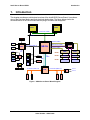


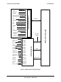
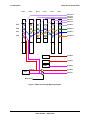

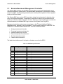
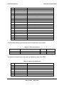
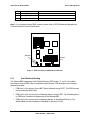
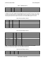


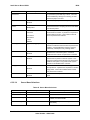
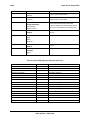

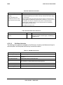
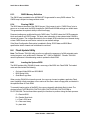

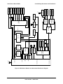

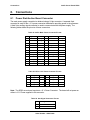

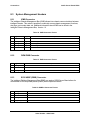
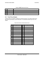
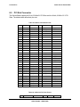
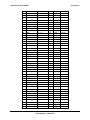
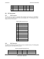
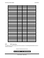
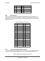

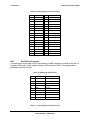


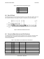
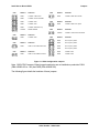


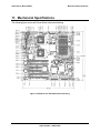


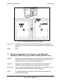


![Streamit Maven user manual [firmware version 2.22.0]](http://vs1.manualzilla.com/store/data/006918496_1-ec2babbff5a065a03e66471e2de505b7-150x150.png)