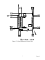
1
PCM-3370
LV Intel Pentium III/ ULV Celeron
PC/104+ CPU Module
User’s Manual
Copyright
This document is copyrighted, © 2003. All rights are reserved. The original manufacturer reserves the right to make improvements to the products
described in this manual at any time without notice.
No part of this manual may be reproduced, copied, translated or transmitted in any form or by any means without the prior written permission of
the original manufacturer. Information provided in this manual is
intended to be accurate and reliable. However, the original manufacturer
assumes no responsibility for its use, nor for any infringements upon the
rights of third parties that may result from such use.
Acknowledgements
Award is a trademark of Award Software International, Inc.
VIA is a trademark of VIA Technologies, Inc.
IBM, PC/AT, PS/2 and VGA are trademarks of International Business
Machines Corporation.
Intel and Pentium are trademarks of Intel Corporation.
Microsoft Windows® is a registered trademark of Microsoft Corp.
RTL is a trademark of Realtek Semi-Conductor Co., Ltd.
ESS is a trademark of ESS Technology, Inc.
UMC is a trademark of United Microelectronics Corporation.
SMI is a trademark of Silicon Motion, Inc.
Creative is a trademark of Creative Technology LTD.
All other product names or trademarks are properties of their respective
owners.
For more information on this and other Advantech products, please visit
our websites at:
http://www.advantech.com
http://www.advantech.com/epc
For technical support and service, please visit our support website at:
http://support.advantech.com
Part No. 2006337001
2nd Edition, April 2004
PCM-3370 User’s Manual
ii
Packing List
Before you begin installing your card, please make sure that the following
materials have been shipped:
• 1 PCM-3370 all-in one single board computer
• 1 CD-ROM or disks for utility, drivers, and manual (in PDF format)
• 1 warranty certificate
• 1 2.5" IDE flat cable, 44-pin to 44-pin (product no. 1701440350)
• 1 PS/2 keyboard & mouse cable
(product no. 1700060202)
• 2 serial port cables
(product no. 1700100250)
• 1 Y-cable external cable
(product no. 1703060053)
• 1 parallel cable
(product no. 1700260250)
• 1 VGA cable
(product no. 1701160150)
• 1 LAN cable
(product no. 1701100202)
• ATX power cable
(product no. 1703200380)
If any of these items are missing or damaged, contact your distributor or
sales representative immediately.
iii
Additional Information and Assistance
Step 1. Visit the Advantech web site at www.advantech.com where you
can find the latest information about the product.
Step 2. Contact your distributor, sales representative, or Advantech's customer service center for technical support if you need additional
assistance. Please have the following information ready before
you call:
• Product name and serial number
• Description of your peripheral attachments
• Description of your software (operating system, version, application
software, etc.)
• A complete description of the problem
• The exact wording of any error messages
PCM-3370 User’s Manual
iv
Safety Instructions
1. Read these safety instructions carefully.
2. Keep this User's Manual for later reference.
3. Disconnect this equipment from any AC outlet before cleaning. Use a damp
cloth. Do not use liquid or spray detergents for cleaning.
4. For plug-in equipment, the power outlet socket must be located near the
equipment and must be easily accessible.
5. Keep this equipment away from humidity.
6. Put this equipment on a reliable surface during installation. Dropping it or letting it fall may cause damage.
7. The openings on the enclosure are for air convection. Protect the equipment
from overheating. DO NOT COVER THE OPENINGS.
8. Make sure the voltage of the power source is correct before connecting the
equipment to the power outlet.
9. Position the power cord so that people cannot step on it. Do not place anything
over the power cord.
10. All cautions and warnings on the equipment should be noted.
11. If the equipment is not used for a long time, disconnect it from the power
source to avoid damage by transient overvoltage.
12. Never pour any liquid into an opening. This may cause fire or electrical shock.
13. Never open the equipment. For safety reasons, the equipment should be
opened only by qualified service personnel.
14. If one of the following situations arises, get the equipment checked by service
personnel:
a. The power cord or plug is damaged.
b. Liquid has penetrated into the equipment.
c. The equipment has been exposed to moisture.
d. The equipment does not work well, or you cannot get it to work according
to the user's manual.
e. The equipment has been dropped and damaged.
f. The equipment has obvious signs of breakage.
15. DO NOT LEAVE THIS EQUIPMENT IN AN ENVIRONMENT WHERE
THE STORAGE TEMPERATURE MAY GO BELOW -20° C (-4° F) OR
ABOVE 60° C (140° F). THIS COULD DAMAGE THE EQUIPMENT. THE
EQUIPMENT SHOULD BE IN A CONTROLLED ENVIRONMENT.
16. CAUTION: DANGER OF EXPLOSION IF BATTERY IS INCORRECTLY
REPLACED.REPLACE ONLY WITH THE SAME OR EQUIVALENT
TYPE RECOMMENDED BY THE MANUFACTURER, DISCARD USED
BATTERIES ACCORDING TO THE MANUFACTURER'S INSTRUCTIONS.
The sound pressure level at the operator's position according to IEC 704-1:1982 is
no more than 70 dB (A).
DISCLAIMER: This set of instructions is given according to IEC 704-1. Advantech disclaims all responsibility for the accuracy of any statements contained
herein.
v
Wichtige Sicherheishinweise
1. Bitte lesen sie Sich diese Hinweise sorgfältig durch.
2. Heben Sie diese Anleitung für den späteren Gebrauch auf.
3. Vor jedem Reinigen ist das Gerät vom Stromnetz zu trennen. Verwenden Sie
Keine Flüssig-oder Aerosolreiniger. Am besten dient ein angefeuchtetes Tuch
zur Reinigung.
4. Die NetzanschluBsteckdose soll nahe dem Gerät angebracht und leicht
zugänglich sein.
5. Das Gerät ist vor Feuchtigkeit zu schützen.
6. Bei der Aufstellung des Gerätes ist auf sicheren Stand zu achten. Ein Kippen
oder Fallen könnte Verletzungen hervorrufen.
7. Die Belüftungsöffnungen dienen zur Luftzirkulation die das Gerät vor überhitzung schützt. Sorgen Sie dafür, daB diese Öffnungen nicht abgedeckt werden.
8. Beachten Sie beim. AnschluB an das Stromnetz die AnschluBwerte.
9. Verlegen Sie die NetzanschluBleitung so, daB niemand darüber fallen kann.
Es sollte auch nichts auf der Leitung abgestellt werden.
10. Alle Hinweise und Warnungen die sich am Geräten befinden sind zu
beachten.
11. Wird das Gerät über einen längeren Zeitraum nicht benutzt, sollten Sie es vom
Stromnetz trennen. Somit wird im Falle einer Überspannung eine Beschädigung vermieden.
12. Durch die Lüftungsöffnungen dürfen niemals Gegenstände oder Flüssigkeiten
in das Gerät gelangen. Dies könnte einen Brand bzw. elektrischen Schlag auslösen.
13. Öffnen Sie niemals das Gerät. Das Gerät darf aus Gründen der elektrischen
Sicherheit nur von authorisiertem Servicepersonal geöffnet werden.
14. Wenn folgende Situationen auftreten ist das Gerät vom Stromnetz zu trennen
und von einer qualifizierten Servicestelle zu überprüfen:
a - Netzkabel oder Netzstecker sind beschädigt.
b - Flüssigkeit ist in das Gerät eingedrungen.
c - Das Gerät war Feuchtigkeit ausgesetzt.
d - Wenn das Gerät nicht der Bedienungsanleitung entsprechend funktioniert
oder Sie mit Hilfe dieser Anleitung keine Verbesserung erzielen.
e - Das Gerät ist gefallen und/oder das Gehäuse ist beschädigt.
f - Wenn das Gerät deutliche Anzeichen eines Defektes aufweist.
15. VOSICHT: Explisionsgefahr bei unsachgemaben Austausch der Batterie.Ersatz nur durch densellben order einem vom Hersteller empfohlenemahnlichen Typ. Entsorgung gebrauchter Batterien navh Angaben des
Herstellers.
Der arbeitsplatzbezogene Schalldruckpegel nach DIN 45 635 Teil 1000
beträgt 70dB(A) oder weiger.
DISCLAIMER: This set of instructions is given according to IEC704-1.
Advantech disclaims all responsibility for the accuracy of any statements
contained herein.
PCM-3370 User’s Manual
vi
Caution!
Danger of explosion if battery is incorrectly
replaced. Replace only with the same or equivalent type recommended by the manufacturer.
Dispose of used batteries according to the manufacturer’s instructions.
vii
PCM-3370 User’s Manual
viii
Content
Chapter
1 General Information ........................................2
1.1
1.2
1.3
1.4
Introduction ....................................................................... 2
Features ............................................................................. 3
Specifications .................................................................... 4
Board Dimensions ............................................................. 6
Figure 1.1:Board Dimensions (Component Side)........... 6
Figure 1.2:Board Dimensions (Solder Side)................... 7
Chapter
2 Installation ......................................................10
2.1
Jumpers............................................................................ 10
2.2
Locating jumpers and connectors.................................... 12
2.3
Setting Jumpers ............................................................... 13
2.4
CPU ................................................................................. 14
Table 2.1:connectors and jumpers ................................ 10
Figure 2.1:Locating Connectors and Jumpers .............. 12
Figure 2.2:Locating Connectors (Solder Side) ............. 13
2.4.1
2.4.2
2.4.3
2.5
CMOS clear (JP1)......................................................... 15
PCI VIO Select (JP3).................................................... 15
Table 2.3:PCI VIO Select (JP3).................................... 15
COM1 and COM2 RI Input Select (JP4, JP5) .............. 16
Table 2.4:COM1 and COM2 RI Input Select (JP4, JP5)..
16
Table 2.5:COM1 and COM2 RI Input Select (JP4, JP5)..
16
SDRAM installation........................................................ 16
2.5.1
SODIMM DRAM ......................................................... 17
2.6
Primary (2.5") IDE connector (CN12) ............................ 17
2.7
2.8
2.9
LPT1 (primary parallel port) connector ............. (CN14)17
Keyboard/mouse connectors (CN17) .............................. 17
Power connectors (CN15, CN18).................................... 18
2.6.1
2.9.1
2.9.2
2.10
Connecting the hard drive............................................. 17
Main power connector (CN15) ..................................... 18
ATX standby power input connector (CN18)............... 18
Serial (COM1,COM2) (CN13,CN16)............................. 18
2.10.1 Primary(COM1:CN20/CN21,COM2:CN14/CN16) ..... 18
2.11
2.12
COM2 422/485 (CN6) .................................................... 18
VGA interface connections ............................................. 18
2.12.1 CRT display connector (CN8) ...................................... 18
2.12.2 Flat panel display connector (CN7,CN20) ................... 18
2.12.3 Invert Power Connector (CN2)..................................... 19
2.13
Ethernet configuration..................................................... 19
ix
2.13.1 Ethernet connector (CN5)............................................. 19
2.13.2 Network boot ................................................................ 19
2.14
Watchdog timer configuration ........................................ 19
2.14.1 Watchdog timer action (JP2) ........................................ 19
Table 2.6:Watchdog Function J2 .................................. 19
2.15
2.16
USB connector (CN26,CN27)......................................... 20
Reset Connector (CN1) .................................................. 20
2.17
2.18
IR Connector (CN3) ........................................................ 20
FAN Connector (CN4) .................................................... 20
Table 2.7:Reset Connector............................................ 20
2.18.1 Power Switch Connector (CN19) ................................. 20
2.18.2 Negative Power Input ................................................... 20
2.18.3 RTC Connector (CN22)................................................ 21
Chapter
3 Software Configuration .................................24
3.1
3.2
Introduction ..................................................................... 24
VGA display firmware configuration ............................. 24
3.3
Connections for four standard LCDs .............................. 26
3.4
Ethernet software configuration ...................................... 30
Figure 3.1:VGA setup screen........................................ 25
Table 3.1:Sharp LM64183P LCD (CN35) ................... 26
Chapter
4 Award BIOS Setup.........................................32
4.1
System test and initialization........................................... 32
4.1.1
4.2
System configuration verification................................. 32
Award BIOS setup .......................................................... 33
4.2.1
Entering setup ............................................................... 33
Figure 4.1:Setup Program Initial Screen....................... 33
4.2.2 Standard CMOS setup .................................................. 33
Figure 4.2:CMOS Setup Screen.................................... 34
4.2.3 BIOS features setup ...................................................... 35
Figure 4.3:BIOS Features Setup Screen ....................... 35
4.2.4 Chipset features setup ................................................... 36
Figure 4.4:ChipsetFeatures Setup Screen ..................... 36
4.2.5 Power management setup ............................................. 37
Figure 4.5:Power Management Setup Screen............... 37
4.2.6 PnP/PCI configuration setup......................................... 38
Figure 4.6:PCI configuration setup screen ................... 38
4.2.7 Integrated peripherals ................................................... 39
Figure 4.7:Integrated peripherals setup screen ............. 39
4.2.8 Load Optimized Defaults BIOS.................................... 40
Figure 4.8:Load Optimized Default BIOS screen ........ 40
4.2.9 Set Password ................................................................. 40
4.2.10 Save & exit setup ......................................................... 41
Figure 4.9:Save and Exit Setup Screen......................... 41
4.2.11 Quit without saving....................................................... 42
PCM-3370 User’s Manual
x
Figure 4.10:Quit Setup Screen...................................... 42
Chapter
5 AGP 4X Setup.................................................44
5.1
Introduction ..................................................................... 44
5.1.1
5.1.2
5.1.3
5.1.4
5.2
Installation of the SVGA Driver ..................................... 46
5.2.1
5.2.2
5.2.3
5.2.4
5.2.5
5.3
Chapter
Chipset .......................................................................... 44
Display memory............................................................ 44
Display types................................................................. 44
Dual/Simultaneous Display .......................................... 45
Figure 5.1:Selecting Display Settings........................... 45
Installation for Windows 95 ......................................... 46
Installation for Windows 98/Me ................................... 50
Installation for Windows NT ........................................ 55
Installation for Windows 2000 ..................................... 60
Installation for Windows XP ........................................ 65
Further Information ......................................................... 71
6 PCI Bus Ethernet Interface...........................74
6.1
6.2
Introduction ..................................................................... 74
Installation of Ethernet Driver......................................... 74
6.2.1
6.2.2
6.2.3
6.2.4
6.3
Installation for MS-DOS and Windows 3.1.................. 74
Installation for Windows 95 ......................................... 75
Installation for Windows 2000 ..................................... 78
Installation for Windows NT ........................................ 83
Further information ......................................................... 87
Appendix A Programming the Watchdog Timer .............90
A.1
Programming the watchdog timer ................................... 90
Appendix B PCM-3370F Jumper Settings ........................92
B.1
B.2
B.3
B.4
B.5
B.6
B.7
B.8
B.9
B.10
B.11
B.12
B.13
B.14
B.15
B.16
CN1 Reset Connector...................................................... 93
CN2 Inverter Power Connector....................................... 93
CN3 IR Connector........................................................... 94
CN4 FAN Connector....................................................... 94
CN5 LAN Connector ...................................................... 95
CN6 422/485 Connector.................................................. 96
CN7 40-Pin LCD Port (24bit) ......................................... 96
CN8 CRT Connector...................................................... 97
CN9 USB Connector....................................................... 98
CN10 20-Pin LCD Connector (36-bit)............................ 99
CN11 PC/104+ Connector .............................................. 99
CN12 44-Pin IDE Connector ........................................ 101
CN13 COM2 RS232 Connector.................................... 102
CN14 LPT Connector.................................................... 102
CN15 Power Conector .................................................. 103
CN16 COM1 RS232 Connector.................................... 104
xi
B.17
B.18
B.19
B.20
B.21
B.22
B.23
B.24
B.25
B.26
B.27
CN17 KB/MS Connector .............................................. 105
CN18 ATX Power Connector ....................................... 105
CN19 Power Switch Connector .................................... 106
CN20 Negative Power Input ......................................... 106
CN21 Compact Flash Slot............................................. 106
CN22 RTC Connector................................................... 108
JP1 COMS Charge&Discharge..................................... 108
JP2 Watchdog Timer..................................................... 108
JP3 PCI VIO Select ....................................................... 109
JP4 COM1 RI Input Select............................................ 109
JP5 COM2 RI Input Select............................................ 110
Appendix C System Assignments .....................................112
C.1
C.2
C.3
C.4
System I/O ports............................................................ 112
DMA channel assignments............................................ 113
Interrupt assignments .................................................... 114
1st MB memory map..................................................... 115
PCM-3370 User’s Manual
xii
CHAPTER
1
General Information
This chapter gives background information on the PCM-3370.
Sections include:
• Sections include:
• Introduction
• Features
• Specifications
• Board layout and dimensions
Chapter 1 General Information
1.1 Introduction
The PCM-3370 utilizes a PC/104+ form factor design that supports ULV
Celeron 400/650 processors and LV Pentium III 800, 933 processors.
This effective PC/104+ solution gives end users the choice of good, economical performance with the ULV Celeron series processors, or the
impressive performance of the LV Pentium III series. These processor
flexibility combined with all the other on-board features, explains why
the PCM-3370 is the new top-of-the-line PC/104+ CPU module solution
at Advantech.
The PCM-3370 is loaded with special on-board features that rival fullsize systems. It has standard 10/100Base-T PCI Ethernet, 36-bit DSTN/
TFT LCD panel support as well as SSD support for CompactFlash. There
is PC/104 and PC/104+ socket for optional international version. The
PCM-3370 also includes 1 SODIMM sockets for up to 512MB total onboard memory.
The PCM-3370 was designed using feedback and knowledge gained from
our customers. It has more of the features our customers have requested.
It is 100% PC compatible and is ready to handle the most challenging
customer driven environments. Besides the great onboard memory flexibility and capacity, the PCM-3370 has four on-board serial ports, each
with +5 V power, two USB connectors, watchdog timer and tough industrial grade construction. The Award 256 KB Flash BIOS supports Plug &
Play, Boot from Ethernet, Boot from CD-ROM, Boot from Zip drive,
Wake-on-Lan, Modem and LCD backlight turnoff. All these features
make the PCM-3370 a very "system integrator friendly" solution, perfect
for handling medical, DVR, Industrial automation and transportation
applications in the harshest unmanned environments.
PCM-3370 User’s Manual
2
1.2 Features
• All-in-one design simplifies system integration and increases system
stability
• Supports ULV Celeron 400/650 and LV Pentium III 800/933 processors.
• Supports on-board features such as 1 x RS-232&1 x RS-232/422/485
with power and 2 x USB interfaces for external peripherals.
• 100/10Base-T with RJ-45 connection for the most demanding networking environment
• Supports PC/104 and PC/104+ for optional PC/104 and PC/104+ perpherial module
• Supports wake-on LAN, modem
• Special industrial features not found on conventional motherboards
include watchdog timer and SSD
• Standardized layout conforms to PC/104 and PC/104+ format for easy
installation within standard sized chassis
• Supports up to 36-bit DSTN/TFT high resolution LCDs
• Advanced CPU switching power technology for stable and low heat
CPU voltage power conversion
• Supports CompactFlash® card
3
Chapter 1
1.3 Specifications
Standard SBC functions
• CPU: On-board ULV Intel Celeron 400/650 (Fanless) / LV Pentium III
800/933 processor
• BIOS: Award 256 KB Flash memory
• Chipset: VIA 8606/TwisterT, VT82C686B
• System memory: One SODIMM sockets accept 32 MB ~ 512MB
SDRAM
• Enhanced IDE interface: Supports up to two EIDE devices. BIOS
auto-detect, PIO Mode 3 or Mode 4, UDMA/33 transfer
• Serial ports: Two serial RS-232 ports, COM1, 4: RS-232, COM2: RS232/422/485
• Parallel port: One parallel ports, supports SPP/EPP/ECP mode
• Infrared port: Shared with COM2. Transfer rates up to 1.15 Mbps
• Keyboard/mouse connector: Supports standard PS/2 keyboard and a
PS/2 mouse
• Power management: Supports power saving modes including Normal/
Standby/Suspend modes. APM 1.1 compliant
• Watchdog timer: 1.6 sec. intervals generate system reset or IRQ11
• USB: Two universal serial bus ports (USB1.1)
Solid state disk
• Supports one 50-pin socket for CompactFlash™ card
VGA/LCD interface
• Chipset: VIA VT8606/TwisterT, optimized Shared Memory Architecture, support 8/16/32 MB frame buffer using system memory.
• Interface: 4X AGP interface
• Display mode: Flat panel displays up to 600 x 480 @ 18 bpp 800 x 600
@ 18 bpp, 1024 x 768 @ 18 bpp, CRT monitors up to 800 x 600 @ 24
bpp, 1024 x 768 @ 16 bpp, 1280 x 1024@16 bpp
Ethernet interface
• Chipset: Reatlek RTL8139D
• Ethernet interface: PCI 10/100 Mbps Ethernet. IEEE 802.3 U protocol compatible
PCM-3370 User’s Manual
4
• Connection: On-board RJ-45 connector
• Built-in boot ROM
Mechanical and environmental
• Max. power requirements:[email protected] for Intel Celeron ULV 400 @
128M
• Operating temperature: 0 ~ 60° C (32 ~ 140° F)
• Dimensions (L x W): 96 mm x 115 mm (3.77" x 4.05")
• Weight: 0.2Kg (0.48lb)
5
Chapter 1
1.4 Board Dimensions
Figure 1.1: Board Dimensions (Component Side)
PCM-3370 User’s Manual
6
Figure 1.2: Board Dimensions (Solder Side)
7
Chapter 1
PCM-3370 User’s Manual
8
CHAPTER
2
Installation
This chapter explains how to set up the
PCM-3370 hardware, including
instructions on setting jumpers and
connecting peripherals, switches and
indicators. Be sure to read all the safety
precautions before you begin the installation procedure.
Chapter 2 Installation
2.1 Jumpers
The PCM-3370 has a number of jumpers that allow you to configure your
system to suit your application. The table below lists the function of each
of the board's connectors and jumpers
Table 2.1: connectors and jumpers
Label
Function
CN1
Reset connector
CN2
Invert power connector
CN3
IR connector
CN4
FAN connector
CN5
LAN hard disk connector
CN6
422/485 connector
CN7
40-pin LCD port (24bit)
CN8
CRT
CN9
USB connector
CN10
20-Pin LCD connector (36-bit)
CN11
PC/104+ connector
CN12
44-pin IDE connector
CN13
COM2 RS232 connector
CN14
LPT connector
CN15
Power Connector
CN16
COM1 RS232 connector
CN17
KB/MS connector
CN18
ATX power connector
CN19
Power Switch connector
CN20
Negative Power input
CN21
Compact Flash Slot
CN22
RTC connector
JP1
CMOS Charge&Discharge
PCM-3370 User’s Manual
10
JP2
Watchdog Timer
JP3
PCI VIO SELECT
JP4
COM1 RI Input Select
JP5
COM2 RI Input Select
11
Chapter 2
2.2 Locating jumpers and connectors
CN2
J P1
CN1 J P2
J P3
CN3
CN4
CN2
CN22
CN5
CN6
CN8
CN9
CN1 3
CN15
CN1 4
CN1 1
CN1 6
CN17
J P4
J P5
CN1 9
CN2 0
CN1 8
Figure 2.1: Locating Connectors and Jumpers
PCM-3370 User’s Manual
12
BT1
CN21
DI MM1
Figure 2.2: Locating Connectors (Solder Side)
2.3 Setting Jumpers
You configure your board to match the needs of your application by setting jumpers. A jumper is the simplest kind of electric switch. It consists
of two metal pins and a small metal clip (often protected by a plastic
cover) that slides over the pins to connect them. To ìcloseî a jumper you
connect the pins with the clip. To ìopenî a jumper you remove the clip.
Sometimes a jumper will have three pins, labeled 1, 2, and 3. In this case
you would connect either pins 1 and 2 or 2 and 3.
13
Chapter 2
open
closed
closed 2-3
The jumper settings are schematically depicted in this manual as follows:
open
closed
closed 2-3
A pair of needle-nose pliers may be helpful when working with jumpers.
If you have any doubts about the best hardware configuration for your
application, contact your local distributor or sales representative before
you make any changes.
Generally, you simply need a standard cable to make most connections.
2.4 CPU
There are 4 CPU can be on-board. ULV Intel Celeron 400/650 and LV
Intel Pentium III 800/933.
Warning!
Always disconnect the power cord from your
chassis when you are working on it. Do not make
connections while the power is on as sensitive
electronic components can be damaged by the
sudden rush of power. Only experienced electronics personnel should open the PC chassis
PCM-3370 User’s Manual
14
Caution!
Always ground yourself to remove any static
charge before touching the PC board. Modern
electronic devices are very sensitive to static
electric charges. Use a grounding wrist strap at
all times. Place all electronic components on a
static-dissipative surface or in a static-shielded
bag when they are not in the chassis.
Warning!
To avoid damaging the computer, always turn off
the power supply before setting “Clear CMOS.”
Set the jumper back to “3V Battery On” before
turning on the power supply.
2.4.1 CMOS clear (JP1)
Table 2.2: JP2 Watchdog Timer
Pin
Function
1-2
Reset *
2-3
IRQ11
1
2
3
1
2
3
IRQ11
RESET*
2.4.2 PCI VIO Select (JP3)
It is a PCI I/O voltage selection. It has VCC(+5V), VCC3(+3.3V) and
NULL.
Table 2.3: PCI VIO Select (JP3)
JP3
PCI VIO SELECT
Pin
Function
1-2
VCC
2-3
VCC3
Default
NULL *
15
Chapter 2
2.4.3 COM1 and COM2 RI Input Select (JP4, JP5)
There is Ring input select jumper at COM1 and COM2.
Table 2.4: COM1 and COM2 RI Input Select (JP4, JP5)
JP4
COM1 RI Input Select
Pin
Function
1-2
RI *
2-3
VCC
Table 2.5: COM1 and COM2 RI Input Select (JP4, JP5)
JP5
COM2 RI Input Select
Pin
Function
1-2
RI *
2-3
VCC
2.5 SDRAM installation
There are one on-board 144-pin SODIMM socket.
PCM-3370 User’s Manual
16
2.5.1 SODIMM DRAM
You can install one DiMM (up to 512 MB).
Caution!
When installing SODIMM, make sure the module
is oriented properly. Do not use excess force during installation.
2.6 Primary (2.5") IDE connector (CN12)
The 44-pin IDE connector supports up to two 44-pin IDE interface
devices, including CD-ROM drives, tape-backup drives, HDDs, etc.
When connecting, make sure pin 1 of the connector is matched with pin
of the device's connector.
The built-in Enhanced IDE (Integrated Device Electronics) controller
supports up to two IDE devices, including CD-ROM drives, tape backup
drives, a large hard disk drive and other IDE devices. It also supports
faster data transfer rates and allows IDE hard disk drives with capacities
in excess of 528 MB.
2.6.1 Connecting the hard drive
Connecting drives is done in a daisy-chain fashion. Wire number 1 on the
cable is red or blue, while the other wires are gray.
Unlike floppy drives, IDE hard drives can connect to either end of the
cable. If you install two drives, you will need to set one as the master and
one as the slave by using jumpers on the drives. If you install just one
drive, set it as the master.
2.7 LPT1 (primary parallel port) connector (CN14)
The primary parallel printer port is located at the rear edge of the board,
and has a 26pin box header connector. This printer port is typically used
to connect a printer via an adapter cable. LPT1's IRQ setting is defined as
IRQ7. You can select Normal/EPP/ECP for LPT1, and enable/disable it in
BIOS (see Chapter 4).
2.8 Keyboard/mouse connectors (CN17)
There is an internal 6 pin KB/Mouse connector (CN17). It need to use Ytype connector to connect Keyboard and mouse.
17
Chapter 2
2.9 Power connectors (CN15, CN18)
2.9.1 Main power connector (CN15)
The power connection is a 8-pin connector requiring +5 V and +12 V
power. It needs a cable (1703080104 for AT or 1703200380 for ATX) to
connect AT/ATX power supply.
2.9.2 ATX standby power input connector (CN18)
The power connection is a 3-pin connector requiring +5 V standby
2.10 Serial (COM1,COM2) (CN13,CN16)
The PCM-3370 has a total of two on-board RS-232 serial ports, COM1
and COM2. They are COM1(RS-232) and COM2 (RS-232/422/485).
Both serial ports have +5 V power capabilities on both pin #1.
2.10.1 Primary(COM1:CN20/CN21,COM2:CN14/CN16)
Each primary serial port has internal 10-pin header giving the user the
ability to adapt the board to many different systems. IRQ for COM1 and
COM2 is fixed with COM1 on IRQ4 and COM2 on IRQ3. COM1 and
COM2 can be enabled or disabled via BIOS (see Chapter 4).
2.11 COM2 422/485 (CN6)
There is a 4-pin boxheader connector for COM2 RS-422/485 connection
purpose.
2.12 VGA interface connections
The PCM-3370 's AGP 4X interface can drive conventional CRT displays
and is capable of driving a wide range of flat panel displays, including
electroluminescent (EL), gas plasma, passive LCD and active LCD displays. The board has two connectors to support these displays, one for
standard CRT VGA monitors and one for flat panel displays.
2.12.1 CRT display connector (CN8)
CN8 is a standard 16-pin (2x8) box header connector commonly used for
the CRT VGA monitor only. Pin assignments appear in the appendix.
2.12.2 Flat panel display connector (CN7,CN20)
PCM-3370 User’s Manual
18
CN7 is 40-pin Hirose connector and CN10 is 20-pin Hirose connector. It
can connect to a 36-bit TFT LCD panel. Pin assignments appear in the
appendix. (For more information on LCD connection information
between CN7 and CN10 and an LCD, refer to Chapter 3.)
2.12.3 Invert Power Connector (CN2)
The PCM-33701F inverter power connector is a 5-pin boxheader.
2.13 Ethernet configuration
The PCM-3370 is equipped with a high performance 32-bit PCI-bus
Ethernet interface which is fully compliant with IEEE 802.3 u
10/100Mbps CSMA/CD standards. It is supported by all major network
operating systems.
The medium type can be configured via the RSET8139.EXE program
included on the utility disk (see Chapter 3 for detailed information).
2.13.1 Ethernet connector (CN5)
100/10Base-T connects to the PCM-3370 via an internal 10pin box
header and use the cable link ot RJ-45 standard jack.
2.13.2 Network boot
The Network Boot feature can be utilized by incorporating the Boot
ROM image files for the appropriate network operating system. The Boot
ROM BIOS files are on the included utility disk.
2.14 Watchdog timer configuration
An onboard watchdog timer reduces the chance of disruptions which
EMP (electro-magnetic pulse) interference can cause. This is an invaluable protective device for standalone or unmanned applications. Setup
involves one jumper and running the control software (refer to Appendix
A).
2.14.1 Watchdog timer action (JP2)
When the watchdog timer activates (CPU processing has come to a halt),
it can reset the system or generate an interrupt on IRQ11. This can be set
via setting J2 as shown below:
Table 2.6: Watchdog Function J2
Closed pins
Result
1-2
Reset*
19
Chapter 2
Table 2.6: Watchdog Function J2
2-3
IRQ11
2.15 USB connector (CN26,CN27)
The PCM-3370 board provides two USB (Universal Serial Bus) interfaces which support plug and play and hot attach/detach for up to 127
external devices. The USB interfaces comply with USB specification
Rev. 1.1 and are fuse protected.
The USB interfaces are accessed through 10-pin (5x2) flat-cable connectors, CN9. You will need an adapter cable if you use a standard USB connector. The adapter cable has a 5-pin connector on one end and a USB
connector on the other.
The USB interfaces can be disabled in the system BIOS setup.
2.16 Reset Connector (CN1)
Table 2.7: Reset Connector
Pin
Pin name
1
Signal
2
Gnd
2.17 IR Connector (CN3)
PCM-3370F's IR is a 5pin boxheader. There is more detail pin assignment
at Appendix.
2.18 FAN Connector (CN4)
The PCM-3370F's FAN connector has speed detect and +5V power input.
It is a 3 pin connector for FAN.
2.18.1 Power Switch Connector (CN19)
There is a PCM-3370F 2-pin power switch at CN19.
2.18.2 Negative Power Input
PCM-3370F can have -5V and -12V negative power input from outside
power supply then it can drive stacking module -5V/-12V from PC/104
socket. It is a 3-pin box header.
PCM-3370 User’s Manual
20
2.18.3 RTC Connector (CN22)
PCM-3370F has a 2-pin boxheader real time clock connector.
21
Chapter 2
PCM-3370 User’s Manual
22
CHAPTER
3
Software Configuration
This chapter details the software configuration information. It shows you
how to configure the card to match
your application requirements. Award
System BIOS will be covered in
Chapter 4.
Sections include:
• Introduction
• VGA display software configuration
• LCD display configuration
• Connections for four standard LCDs
• Ethernet interface configuration
Chapter 3 Software Configuration
3.1 Introduction
The PCM-3370 system BIOS and custom drivers are located in a
256 KB, 32-pin (JEDEC spec.) Flash ROM device, designated U23. A
single Flash chip holds the system BIOS, VGA BIOS, and network Boot
ROM image. The display can be configured via software. This method
minimizes the number of chips and eases configuration. You can change
the display BIOS simply by reprogramming the Flash chip.
3.2 VGA display firmware configuration
The PCM-3370’s on-board VGA interface supports a wide range of popular LCD, EL, gas plasma flat panel displays and traditional analog CRT
monitors. The optimized shared memory architecture supports an 8/16/32
MB frame buffer using system memory to provide resolutions of 1280 x
1024 @ 16 bpp, the interface can drive CRT displays with resolutions up
to 1024 x 768 @ 16 bpp and 800 x 600 @ 16 bpp.
The VGA interface is configured completely via the software utility, so
you do not have to set any jumpers. Configure the VGA display as follows:
1.
Apply power to the PCM-3370 with a color TFT display attached.
This is the default setting for the PCM-3370. Ensure that the AWDFLASH.EXE and *.BIN files are located in the working drive.
NOTE:
Ensure that you do not run AWDFLASH.EXE
while your system is operating in EMM386
mode.
PCM-3370 User’s Manual
24
2.
At the prompt, type AWDFLASH.EXE and press <Enter>. The
VGA configuration program will then display the following:
Figure 3.1: VGA setup screen
3.
At the prompt, enter the new BIN file which supports your display.
When you are sure that you have entered the file name correctly
press <Enter>.
4.
The screen will ask ìDo you want to save BIOS?î. If you change
your mind or have made a mistake, press N to abort and end the
setup procedure. Press Y if you wish to save the existing configuration before changing it. Then type the name under which you want
to save the current configuration.
5.
The prompt will then ask ìAre you sure to program?î. Press Y if
you want the new file to be written into the BIOS. Press N to exit
the program.
The new VGA configuration will then write to the ROM BIOS chip. This
configuration will remain the same until you run the AWDFLASH.EXE
program and change the settings.
25
Chapter 3
3.3 Connections for four standard LCDs
Connections to Sharp LM64183P (640 x 480 DSTN MONO LCD)
Table 3.1: Sharp LM64183P LCD (CN35)
LM64183P
PCM-3370 (CN35)
Pin
Name
Pin
Name
CN1-1
S
36
FLM
CN1-2
CP1
38
LP
CN1-3
CP2
35
SHFCLK
CN1-4
DISP
5
+5 V
CN1-5
VDD
6
+5 V
CN1-6
VSS
3
GND
CN1-7
VEE
-
-17 V (external power)
CN1-8
DU0
12
P3
CN1-9
DU1
11
P2
CN1-10
DU2
10
P1
CN1-11
DU3
9
P0
CN1-12
DL0
16
P7
CN1-13
DL1
15
P6
CN1-14
DL2
14
P5
CN1-15
DL3
13
P4
* LM64183P requires -17 V for VEE
Connections to PLANAR EL640.480-AM1 (640 x 480 EL LCD)
Table 3.2: PCM-3370 connection for PLANAR EL LCD (CN35)
PLANAR 640.480-AM1
PCM-3370 (CN35)
Pin
Name
Pin
Name
1
UD1
11
P2
2
UDO
12
P3
3
UD3
9
P0
4
UD2
10
P1
5
LD1
15
P6
6
LD0
16
P7
PCM-3370 User’s Manual
26
Table 3.2: PCM-3370 connection for PLANAR EL LCD (CN35)
7
LD3
13
P4
8
LD2
14
P5
9
CP2
35
SHFCLK
10
GND
33
GND
11
CP1
38
LP
12
GND
33
GND
13
S
36
FLM
14
GND
34
GND
15
GND
3
GND
16
GND
4
GND
17
VL
5
VCC
18
VL
6
VCC
19
VH
1
+12 V
20
VH
2
+12 V
Connections to Toshiba LTM10C209A (640 x 480 TFT color LCD)
Table 3.3: Toshiba LTM10C209A LCD (CN35)
LTM10C209A
PCM-3370 (CN35)
Pin
Name
Pin
Name
1
GND
3
GND
2
CLK
35
SHFCLK
3
GND
4
GND
4
R0
27
P18
5
R1
28
P19
6
R2
29
P20
7
GND
8
GND
8
R3
30
P21
9
R4
31
P22
10
R5
32
P23
11
GND
33
GND
12
G0
19
P10
27
Chapter 3
Table 3.3: Toshiba LTM10C209A LCD (CN35)
13
G1
20
P11
14
G2
21
P12
15
GND
33
GND
16
G3
22
P13
17
G4
23
P14
18
G5
24
P15
19
GND
34
GND
20
ENAB
37
M
21
GND
34
GND
22
B0
11
P2
23
B1
12
P3
24
B2
13
P4
25
GND
39
GND
26
B3
14
P5
27
B4
15
P6
28
B5
16
P7
29
GND
39
GND
30
VDD
5
+5 V
31
VDD
6
+5 V
Connections to Kyocera KCB6446BSTT-X5 (640 x 480 DSTN color
LCD)
Table 3.4: PCM-3370 connection for Kyocera KCB6446BSTT-X5
LCD (CN35)
KCB6446BSTT-X5
PCM-3370 (CN35)
Pin
Name
Pin
Name
CN1-1
FRM
36
FLM
CN1-2
DF
-
-
CN1-3
DISP
40
ENABKL
CN1-4
LOAD
38
LP
CN1-5
VSS
33
GND
CN1-6
CP
35
SHFCLK
PCM-3370 User’s Manual
28
Table 3.4: PCM-3370 connection for Kyocera KCB6446BSTT-X5
LCD (CN35)
CN1-7
VSS
34
GND
CN1-8
HD0
20
P11
CN1-9
HD1
19
P10
CN1-10
HD2
18
P9
CN1-11
HD3
17
P8
CN1-12
HD4
12
P3
CN1-13
HD5
11
P2
CN1-14
HD6
10
P1
CN1-15
HD7
9
P0
CN2-1
LD0
24
P15
CN2-2
LD1
23
P14
CN2-3
LD2
22
P13
CN2-4
LD3
21
P12
CN2-5
LD4
16
P7
CN2-6
LD5
15
P6
CN2-7
LD6
14
P5
CN2-8
LD7
13
P4
CN2-9
VDD
5
VCC
CN2-10
VSS
3
GND
CN2-11
NC
-
-
CN2-12
NC
-
-
CN2-13
NC
-
-
CN2-14
VCONT
*7
*VEESAFE
29
Chapter 3
3.4 Ethernet software configuration
The PCM-3370’s on-board Ethernet interface supports all major network
operating systems. To configure the medium type, to view the current
configuration, or to run diagnostics, do the following:
1.
Power the PCM-3370 on. Ensure that the RSET8139.EXE file is
located in the working drive.
2.
At the prompt type RSET8139.EXE and press <Enter>. The Ethernet configuration program will then be displayed.
3.
This simple screen shows all the available options for the Ethernet
interface. Just highlight the option you wish to change by using the
Up and Down keys. To change a selected item, press <Enter>, and
a screen will appear with the available options. Highlight your
option and press <Enter>. Each highlighted option has a helpful
message guide displayed at the bottom of the screen for additional
information.
4.
After you have made your selections and your are sure that this is
the configuration you want, press ESC. A prompt will appear asking if you want to save the configuration. Press Y if you want to
save.
The Ethernet Setup Menu also offers three very useful diagnostic functions. These are:
1.
Run EEPROM Test.
2.
Run Diagnostics on Board.
3.
Run Diagnostics on Network.
Each option has its own display screen which shows the format and result
of any diagnostic tests undertaken.
PCM-3370 User’s Manual
30
CHAPTER
4
Award BIOS Setup
This chapter describes how to set BIOS
configuration data.
Chapter 4 Award BIOS Setup
4.1 System test and initialization
These routines test and initialize board hardware. If the routines encounter an error during the tests, you will either hear a few short beeps or see
an error message on the screen. There are two kinds of errors: fatal and
non-fatal. The system can usually continue the boot up sequence with
non-fatal errors. Non-fatal error messages usually appear on the screen
along with the following instructions:
press <F1> to RESUME
Write down the message and press the F1 key to continue the bootup
sequence.
4.1.1 System configuration verification
These routines check the current system configuration against the values
stored in the cardís CMOS memory. If they do not match, the program
outputs an error message. You will then need to run the BIOS setup program to set the configuration information in memory.
There are three situations in which you will need to change the CMOS
settings:
1.
You are starting your system for the first time.
2.
You have changed the hardware attached to your system.
3.
The CMOS memory has lost power and the configuration information has been erased.
The PCM-3370’s CMOS memory has an integral lithium battery backup.
The battery backup should last ten years in normal service, but when it
finally runs down, you will need to replace the complete unit.
PCM-3370 User’s Manual
32
4.2 Award BIOS setup
Awardís BIOS ROM has a built-in Setup program that allows users to
modify the basic system configuration. This type of information is stored
in battery-backed CMOS RAM so that it retains the Setup information
when the power is turned off.
4.2.1 Entering setup
Power on the computer and press <Del> immediately. This will allow you
to enter Setup.
Figure 4.1: Setup Program Initial Screen
4.2.2 Standard CMOS setup
When you choose the Standard CMOS Setup option from the Initial
Setup Screen menu, the screen shown below is displayed. This standard
Setup Menu allows users to configure system components such as date,
time, hard disk drive, display, and memory. Once a field is highlighted,
33
Chapter 4
online help information is displayed in the left bottom of the Menu
screen.
Figure 4.2: CMOS Setup Screen
PCM-3370 User’s Manual
34
4.2.3 BIOS features setup
By choosing the BIOS FEATURES Setup option from the Initial Setup
Screen menu, the screen below is displayed. This sample screen contains
the manufacturerís default values for the PCM-3370.
Figure 4.3: BIOS Features Setup Screen
35
Chapter 4
4.2.4 Chipset features setup
By choosing the CHIPSET FEATURES Setup option from the Initial
Setup Screen menu, the screen below is displayed. This sample screen
contains the manufacturerís default values for the PCM-3370.
Figure 4.4: ChipsetFeatures Setup Screen
PCM-3370 User’s Manual
36
4.2.5 Power management setup
By choosing the POWER MANAGEMENT Setup option from the Initial
Setup Screen menu, the screen below is displayed. This sample screen
contains the manufacturerís default values for the PCM-3370.
Figure 4.5: Power Management Setup Screen
37
Chapter 4
4.2.6 PnP/PCI configuration setup
By choosing the PnP/PCI CONFIGURATION option from the Initial
Setup Screen menu, the screen below is displayed. This sample screen
contains the manufacturerís default values for the PCM-3370.
Figure 4.6: PCI configuration setup screen
PCM-3370 User’s Manual
38
4.2.7 Integrated peripherals
By choosing the INTEGRATED PERIPHERALS option from the Initial
Setup Screen menu, the screen below is displayed. This sample screen
contains the manufacturerís default values for the PCM-3370.
Figure 4.7: Integrated peripherals setup screen
39
Chapter 4
4.2.8 Load Optimized Defaults BIOS
LOAD OPTIMIZED DEFAULTS loads the default optimized system values
directly from ROM. If the stored record created by the Setup program
becomes corrupted (and therefore unusable), these defaults will load
automatically when you turn the PCM-3370 on.
Figure 4.8: Load Optimized Default BIOS screen
4.2.9 Set Password
To change the password, choose the SET PASSWORD option form the
Setup main menu and press <Enter>.
1.
If the CMOS is bad or this option has never been used, there is
default password which is stored in the ROM. The screen will display the following messages:
Enter Password
Press <Enter>.
2.
If the CMOS is good or this option has been used to change the
default password, the user is asked for the password stored in the
CMOS. The screen will display the following message:
PCM-3370 User’s Manual
40
Confirm Password
Enter the current password and press <Enter>.
3.
After pressing <Enter> (ROM password) or the current password
(user-defined), you can change the password stored in the CMOS.
The password can be at most 8 characters long.
Remember - to enable this feature, you must first select either Setup or
System in the BIOS FEATURES SETUP.
4.2.10 Save & exit setup
If you select this option and press <Enter>, the values entered in the setup
utilities will be recorded in the chipset's CMOS memory. The microprocessor will check this every time you turn your system on and compare
this to what it finds as it checks the system. This record is required for the
system to operate.
Figure 4.9: Save and Exit Setup Screen
41
Chapter 4
4.2.11 Quit without saving
Selecting this option and pressing <Enter> lets you Quit the Setup program without recording any new values or changing old ones.
Figure 4.10: Quit Setup Screen
PCM-3370 User’s Manual
42
CHAPTER
5
AGP 4X Setup
The PCM-3370 features an onboard
AGP 4X flat panel/VGA interface. This
chapter provides instructions for
installing and operating the software
drivers on the included display driver
diskette.
Chapter 5 AGP 4X Setup
5.1 Introduction
The PCM-3370 has an onboard AGP flat panel/VGA interface. The specifications and features are described as follows:
5.1.1 Chipset
The PCM-3370 uses a VIA Twister 8606T chipset from VIA Technology
Inc. for its AGP/SVGA controller. It supports many popular LCD, and
LVDS LCD displays and conventional analog CRT monitors. The
VIA8606T VGA BIOS supports color TFT and DSTN LCD flat panel
displays. In addition, it also supports interlaced and non-interlaced analog
monitors (color and monochrome VGA) in high-resolution modes while
maintaining complete IBM VGA compatibility. Digital monitors
(i.e. MDA, CGA, and EGA) are NOT supported. Multiple frequency
(multisync) monitors are handled as if they were analog monitors.
5.1.2 Display memory
The Twister chip can support 8/16/32MB frame buffer shared with system memory; the VGA controller can drive CRT displays or color panel
displays with resolutions up to 1280 x 1024 at 16 M colors.
5.1.3 Display types
CRT and panel displays can be used simultaneously. The PCM-3370 can
be set in one of three configurations: on a CRT, on a flat panel display, or
on both simultaneously. The system is initially set to simultaneous display mode. If you want to enable the CRT display only or the flat panel
display only, please contact VIA Technology Inc., or our sales representative for detailed information.
PCM-3370 User’s Manual
44
5.1.4 Dual/Simultaneous Display
The PCM-3370 uses a VIA Twister VT8606T LCD controller that is
capable of providing simultaneous dual view display of the same content
on a flat panel and CRT.
To set up dual view (simultaneus mode) under Windows 9x, Windows
ME, Windows NT/2000/XP, follow these steps:
Step 1. Open the Control panel, and select “Display”, “Settings”.
Step 2. Select " CRT+LCD " or " CRT+TV " for dual view
Step 3. Click “OK”.
1
Figure 5.1: Selecting Display Settings
45
Chapter 5
5.2 Installation of the SVGA Driver
Complete the following steps to install the SVGA driver. Follow the procedures in the flow chart that apply to the operating system that you are
using within your PCM-3370.
Notes:
1. The windows illustrations in this chapter are
intended as examples only. Please follow the
listed steps, and pay attention to the instructions which appear on your screen.
2. For convenience, the CD-ROM drive is designated as "D" throughout this chapter.
5.2.1 Installation for Windows 95
1.
Select "Start", "Settings", "Control Panel", "Display", "Settings”,
and "Advanced Properties".
PCM-3370 User’s Manual
46
2.
Choose the "Adapter" tab, then press the "Change..." button.
3.
Press the "Have Disk" button.
47
Chapter 5
4.
Type in the path:
D:\vga\VT8606\Win9x_Me
5.
Select the highlighted item, and click the "OK" button.
PCM-3370 User’s Manual
48
6.
"S3 GraphicsTwister" appears under the adapter tab. Click the
"Apply" button, then the "OK" button.
7.
Press “Yes” to reboot.
49
Chapter 5
5.2.2 Installation for Windows 98/Me
1.
Select "Start", "Settings", "Control Panel", "Display", and "Settings," then press the "Advanced..." button.
PCM-3370 User’s Manual
50
2.
Select “Adapter,” then “Change.”
51
Chapter 5
3.
Press “Next,” then “Display a list....”
4.
Press the “Have disk...” button.
PCM-3370 User’s Manual
52
5.
Insert the CD into the CD-ROM drive. Type in the path
D:\vga\VT8606\Win9x_Me
Then press “OK”
6.
Select the highlighted item, then click “OK.”
53
Chapter 5
7.
"S3 Graphics Twister"appears under the adapter tab. Click the
"Apply" button.
8.
Press “Yes” to reboot.
PCM-3370 User’s Manual
54
5.2.3 Installation for Windows NT
Note:
1.
Service Pack X (X = 3, 4, 5, 6,...) must be
installed first, before you install the Windows NT
VGA driver.
Select "Start", "Settings", "Control Panel" and double click the
"Display" icon.
55
Chapter 5
2.
Choose the "Settings" tab, and press the "Display Type" button.
PCM-3370 User’s Manual
56
3.
Press the "Change..." button.
57
Chapter 5
4.
Click the "Have Disk..." button.
5.
Type the path:
D:\vga\VT8606\Win NT
Press the "OK" button.
PCM-3370 User’s Manual
58
6.
Select the highlighted item, and click the "OK" button.
7.
Press "Yes" to proceed.
8.
Press "OK" to reboot.
59
Chapter 5
5.2.4 Installation for Windows 2000
1.
Select "System", "Settings", "Control Panel" and double click the
"system" icon.
PCM-3370 User’s Manual
60
2.
Choose the "Video Controller (VGA Compatible)” button.
61
Chapter 5
3.
Choose the "Drive" button, press “Update Driver...” button.
PCM-3370 User’s Manual
62
4.
Choose "Display a list of..." , then press “Next” button.
5.
Choose “Display adapters”, press “Next” button.
63
Chapter 5
6.
Click the “Have Disk” button.
7.
Type the path D:\vga\VT8606\Win2000 press the “OK” button.
PCM-3370 User’s Manual
64
8.
Press “Finish" to reboot.
5.2.5 Installation for Windows XP
1.
Select "System", "Settings", "Control Panel" and double click the
"system" icon.
65
Chapter 5
2.
Choose “Hardware” and “Device Manager”, press “OK” button.
PCM-3370 User’s Manual
66
3.
Choose “Video Controller (VGA Compatible), press “OK” button.
67
Chapter 5
4.
Choose "Driver”, “Update Driver”, press “OK” button.
5.
Choose “Install from a list.....” , press “Next”.
PCM-3370 User’s Manual
68
6.
Choose “Don’t search. I will....”, press “Next” button.
7.
Choose “Display adapters”, press “Next” button.
69
Chapter 5
8.
Type the path D:\vga\VT8606\WinXP then press “OK” button.
9.
Choose “S3 Graphics Twister + S3 Hotkey” then press “Next” button.
PCM-3370 User’s Manual
70
10.
Press “Finish" to reboot.
5.3 Further Information
For further information about the AGP/VGA installation in your PCM3370, including driver updates, troubleshooting guides and FAQ lists,
visit the following web resources:
VIA website:
www.via.com.tw
Advantech websites: www.advantech.com
www.advantech.com.tw
71
Chapter 5
PCM-3370 User’s Manual
72
CHAPTER
6
PCI Bus Ethernet Interface
This chapter provides information on
Ethernet configuration.
• Introduction
• Installation of Ethernet driver for
- MS-DOS
- Windows 3.1
- Windows 95
- Windows 98
- Windows 2000
- Windows NT
• Further information
Chapter 6 PCI Bus Ethernet Interface
6.1 Introduction
The PCM-3370 is equipped with a high-performance 32-bit Ethernet
chipset which is fully compliant with IEEE 802.3 100 Mbps CSMA/CD
standards. It is supported by major network operating systems. It is also
both 100Base-T and 10Base-T compatible. The medium type can be configured via the PQ8139.exe program included on the utility disk.
The Ethernet port provides a standard RJ-45 jack. The network boot feature can be utilized by incorporating the boot ROM image files for the
appropriate network operating system. The boot ROM BIOS files are
combined with system BIOS, which can be enabled/disabled in the BIOS
setup.
6.2 Installation of Ethernet Driver
Before installing the Ethernet driver, note the procedures below. You
must know which operating system you are using in your PCM-3370, and
then refer to the corresponding installation flow chart. Then just follow
the steps described in the flow chart. You will quickly and successfully
complete the installation, even if you are not familiar with instructions for
MS-DOS or Windows.
.
Note:
The windows illustrations in this chapter are
examples only. You must follow the flow chart
instructions and pay attention to the instructions
which then appear on your screen.
6.2.1 Installation for MS-DOS and Windows 3.1
If you want to set up your Ethernet connection under the MS-DOS or
Windows 3.1 environment, you should first check your server system
model. For example, MS-NT, IBM-LAN server, and so on.
Then choose the correct driver to install in your panel PC.
The installation procedures for various servers can be found on CDROM. The file path begins as: D:\LAN\8139C\drive\wfw311
PCM-3370 User’s Manual
74
6.2.2 Installation for Windows 95
1.
a. Select Start/Settings/Control Panel
b. Double click "Network".
2.
a. Click "Add" and prepare to install network functions.
75
Chapter 6
3. a. Select the "Adapter" item to add the Ethernet card.
4. Click "Have Disk" to install the driver.
5.
a. Insert the CD into the D: drive
b. Fill in: D:\LAN\8139C\
c. Click "OK"
PCM-3370 User’s Manual
76
6.
a. Choose the "Realtek" item
b. Click "OK"
7.
a. Make sure the configurations of relative items are set correctly
b. Click "OK" to reboot
Note:
The correct file path for Windows 98 is:
D:\LAN\8138C\WIN98
77
Chapter 6
6.2.3 Installation for Windows 2000
Step 1. Open Device Manager,
PCM-3370 User’s Manual
78
Step 2.
79
Chapter 6
Step 3.
Step 4.
PCM-3370 User’s Manual
80
Step 5.
Step 6.
81
Chapter 6
Step 7.
Step 8.
PCM-3370 User’s Manual
82
Step 9
6.2.4 Installation for Windows NT
1.
a. Select Start/Settings/Control Panel.
b. Double click "Network".
83
Chapter 6
2.
a. Choose the "Adapters" label.
b. Click the "Add" button.
PCM-3370 User’s Manual
84
3
a. Press "Have Disk".
4.
a. Type "D:".
b. Press "OK".
5.
a. Insert the CD into the D: drive.
b. Fill in: D:\LAN\8139C\WINNT4
c. Press the "OK" button.
85
Chapter 6
6.
a. Choose the "Realtek" item.
b. Press the "OK" button.
7.
a. Make sure the configurations of relevant items are set correctly.
b. Press the "OK" button to reboot.
PCM-3370 User’s Manual
86
6.3 Further information
Realtek website: www.realtek.com
Advantech websites:www.advantech.com
www.advantech.com.tw
87
Chapter 6
PCM-3370 User’s Manual
88
Appendix
A
Programming the
Watchdog Timer
The PCM-3370 is equipped with a
watchdog timer that resets the CPU or
generates an interrupt if processing
comes to a standstill for whatever reason. This feature ensures system reliability in industrial standalone or
unmanned environments.
Appendix A Programming the Watchdog
Timer
A.1 Programming the watchdog timer
The following example show how you might program the watchdog timer
in Assembly:
1. Watch Dog Timer Enable
Port 404e Bit7 set "o" to enable PCM-3370 Watch Dog Timer
Ex:
Mov DX, 404e
Mov AL, 7F
Out DX, AL
2. Watch Dog Timer Disable
Port 404e Bit6 set "o" to disable PCM-3370 Watch Dog Timer
Ex:
Mov DX, 404e
Mov AL, BF
Out DX, AL
PCM-3370 User’s Manual
90
Appendix
B
Jumper Settings
The PCM-3370 is equipped with a
watchdog timer that resets the CPU or
generates an interrupt if processing
comes to a standstill for any reason.
This feature ensures system reliability
in industrial standalone or unmanned
environments.
Appendix B PCM-3370F Jumper Settings
Table B.1: Connectors
1.
CN1
Reset Connect
2.
CN2
Invert Power Connect
3.
CN3
IR Connect
CN4
FAN Connector
5.
CN5
LAN Connector
6.
CN6
422/485 Connect
7.
CN7
40-pin LCD Port (24bit)
8.
CN8
CRT Connect
9.
CN9
USB Connector
10.
CN10
20-Pin LCD Connector (36-bit)
11.
CN11
PC/104+ Connector
12.
CN12
44-Pin IDE Connector
13.
CN13
COM2 RS232 Connector
14.
CN14
LPT Connector
15.
CN15
Power Connector
16.
CN16
COM1 RS232 Connector
17.
CN17
KB/MS Connector
18.
CN18
ATX Power Connector
19.
CN19
Power Switch Input
20.
CN20
Negative Power Input
21.
CN21
Compact Flash Slot
22.
CN22
RTC Connector
23.
JP1
CMOS Charge&Discharge
24.
JP2
Watchgdog Timer
25.
JP3
PCI VIOS SELECT
26.
JP4
COM1, RI Input Select
27.
JP5
COM2 RI Input Select
PCM-3370 User’s Manual
92
B.1 CN1 Reset Connector
Table B.2: CN1 Reset Connector
Pin
Pin name
1
Signal
2
GND
1
2
B.2 CN2 Inverter Power Connector
Table B.3: CN2 Inverter Power Connector
1
+12V
2
GND
3
ENABKL
4
VBR
5
+5V
5
4
3
93
2
1
Appendix B
B.3 CN3 IR Connector
Table B.4: IR Connector
1
+5V
2
NC
3
IRRX
4
GND
5
IRTX
5
4
3
2
B.4 CN4 FAN Connector
Table B.5: CN4 FAN Connector
1
SPEED DETECT
2
+5V
3
GND
3
PCM-3370 User’s Manual
2
94
1
1
B.5 CN5 LAN Connector
Table B.6: CN5 LAN Connector
Pin
Pin name
1
VCC_LAN
2
ACTLED
3
RX+
4
RX-
5
LILED
6
GND
7
NC
8
GND
9
TX+
10
TX-
1
3
5
7
9
2
4
6
8
10
95
Appendix B
B.6 CN6 422/485 Connector
Table B.7: CN6 422/485 Connector
1
RX485-
2
RX485+
3
TX485+
4
TX485-
4
3
2
1
B.7 CN7 40-Pin LCD Port (24bit)
Table B.8: CN7 40-Pin LCD Port (24bit)
Pin
Pin name
Pin
Pin name
1
LCD VDD(+5V)
2
LCD VDD(+5V)
3
GND
4
GND
5
LCD VDD(+3.3V)
6
LCD VDD(+3.3V)
7
Vcon(optional)
8
GND
9
PD0
10
PD1
11
PD2
12
PD3
13
PD4
14
PD5
15
PD6
16
PD7
17
PD8
18
PD9
19
PD10
20
PD11
21
PD12
22
PD13
23
PD14
24
PD15
25
PD16
26
PD17
27
PD18
28
PD19
29
PD20
30
PD21
31
PD22
32
PD23
33
GND
34
GND
PCM-3370 User’s Manual
96
35
SHFCLK
36
FLM(V-SYNC)
37
M/(DE)
38
LP(H-SYNC)
39
ENABKL
40
ENVEE
1 3
37 3 9
2 4
38 4 0
B.8 CN8 CRT Connector
Table B.9: CN8 CRT Connector
1
RED
2
DDC POWER(+5V)
3
GREEN
4
GND
5
BLUE
6
NC
7
NC
8
DDC DATA
9
GND
10
H-SYNC
11
GND
12
V-SYNC
13
GND
14
DDC CLOCK
15
GND
16
NC
15 13
3 1
16 14
4 2
97
Appendix B
B.9 CN9 USB Connector
Table B.10: CN9
1
+5V
2
+5V
3
D0-
4
D1-
5
D0+
6
D1+
7
GND
8
GND
9
GND
10
NC
PCM-3370 User’s Manual
USB Connector
10
9
8
6
4
2
7
5
3
1
98
B.10 CN10 20-Pin LCD Connector (36-bit)
Table B.11: CN10 20-Pin LCD Connector (36-bit)
Pin
Pinname
Pin
Pinname
1
GND
2
GND
3
PD24
4
PD25
5
PD26
6
PD27
7
PD28
8
PD29
9
PD30
10
PD31
11
PD32
12
PD33
13
PD34
14
PD35
15
GND
16
GND
17
NC
18
SPCLK
19
PCIRST
20
SPDAT
1 3
17 19
2 4
18 2 0
B.11 CN11 PC/104+ Connector
Table B.12: PC/104+ connectors (CN18)
Pin
Number
Signal
RowA
Signal
Row B
Signal
RowC
Signal
RowD
1
IOCHCHK*
GND
GND
GND
2
SD7
RESET
SBHE*
MEMCS16*
3
SD6
+5 V
LA23
IOCS16*
4
SD5
IRQ9
LA22
IRQ10
5
SD4
-5V
LA21
IRQ11
6
SD3
DRQ2
LA20
IRQ12
7
SD2
-12V
LA19
IRQ15
8
SD1
ENDXFR*
LA18
IRQ14
99
Appendix B
9
SD0
+12V
LA17
DACKO*
10
IOCHRDY
(KEY)
MEMR*
DRQ0
11
AEN
SMEMW*
MEMW*
DACK5*
12
SA19
SMEMR*
SD8
DRQ5
13
SA18
IOW*
SD9
DACK6*
14
SA17
IOR*
SD10
DRQ6
15
SA16
DACK3*
SD11
DACK7*
16
SA15
DRQ3
SD12
DRQ7
17
SA14
DACK1*
SD13
+5V
DRQ1
SD14
MASTER*
* low active
18
SA13
19
SA12
REFRESH*
SD15
0V
20
SA11
SYSCLK
(KEY)
0V
21
SA10
IRQ7
----
----
22
SA9
IRQ6
----
----
23
SA8
IRQ5
----
----
24
SA7
IRQ4
----
----
25
SA6
IRQ3
----
----
26
SA5
DACK2*
----
----
27
SA4
TC
----
----
28
SA3
BALE
----
----
29
SA2
+5V
----
----
30
SA1
OSC
----
----
31
SA0
0V
----
----
32
0V
0V
----
----
8
8
PC/104-Plus connector (PCI bus)
PCM-3370 User’s Manual
100
B.12 CN12 44-Pin IDE Connector
Table B.13: CN12
44-Pin IDE Connector
Pin
Pinname
Pin
Pinname
1
Reset
2
GND
3
D7
4
D8
5
D6
6
D9
7
D5
8
D10
9
D4
10
D11
11
D3
12
D12
13
D2
14
D13
15
D1
16
D14
17
D0
18
D15
19
GND
20
Reserved
21
DMARQ
22
GND
23
DIOW-
24
GND
25
DIOR-
26
GND
27
IORDY
28
SPSYNC:CSEL
29
DMACK-
30
GND
31
INTRQ
32
IOCS16#
33
DA1
34
PDIAG#:N/C
35
DA0
36
DA2
37
CS0-
38
CS1-
39
DASP-
40
GND
41
+5V
42
+5V
43
GND
44
NC
43 41
3 1
44 42
4 2
101
Appendix B
B.13 CN13 COM2 RS232 Connector
Table B.14: CN13 COM2 RS232 Connector
Pin
Pin name
1
DCD
2
DSR
3
RxD
4
RTS
5
TxD
6
CTS
7
DTR
8
RI
9
GND
10
N/C
1
3
5
7
9
2
4
6
8
10
B.14 CN14 LPT Connector
Table B.15: CN14 LPT Connector
Pin
Pin name
Pin
Pin name
1
STROBE-
2
AUTO FEED-
3
Data 0
4
ERROR
5
Data 1
6
INIT-
7
Data 2
8
SLCT IN-
9
Data 3
10
GND
11
Data 4
12
GND
13
Data 5
14
GND
15
Data 6
16
GND
PCM-3370 User’s Manual
102
17
Data 7
18
GND
19
ACK-
20
GND
21
BUSY
22
GND
23
PaperEmpty
24
GND
25
SELECT
26
N/C
25 23
3 1
26 24
4 2
B.15 CN15 Power Conector
Table B.16: CN15
1
+5V
2
+5V
3
+5V
4
GND
5
GND
6
GND
7
GND
8
+12V
Power Conector
87654321
103
Appendix B
B.16 CN16 COM1 RS232 Connector
Table B.17: CN16 COM1 RS232 Connector
Pin
Pin name
1
DCD
2
DSR
3
RXD
4
RTS
5
TXD
6
CTS
7
DTR
8
RI
9
GND
10
N/C
1
3
5
7
9
PCM-3370 User’s Manual
2
4
6
8
10
104
B.17 CN17 KB/MS Connector
Table B.18: CN17 KB/MS Connector
Pin
Pin name
1
KB CLOCK
2
KB DATA
3
MS CLOCK
4
GND
5
+5V
6
MS DATA
6
5
4
3
2
1
B.18 CN18 ATX Power Connector
Table B.19: CN18 ATX Power Connector
Pin
Pin name
1
+5V Standby
2
GND
3
PSON
105
Appendix B
B.19 CN19 Power Switch Connector
Table B.20: CN19 Power Switch Connector
Pin
Pin name
1
Signal
2
GND
1
2
B.20 CN20 Negative Power Input
Table B.21: CN20 Negative Power Input
Pin
Pin name
1
-5V
2
GND
3
-12V
3
2
1
B.21 CN21 Compact Flash Slot
Table B.22: CompactFlash socket (CN21)
Pin
Signal
Pin
Signal
1
GND
2
D03
3
D04
4
D05
5
D06
6
D07
7
*CS0
8
A10
9
*ATA SEL
10
A09
PCM-3370 User’s Manual
106
11
A08
12
A07
13
+5 V
14
A06
15
A05
16
A04
17
A03
18
A02
19
A01
20
A00
21
D00
22
D01
23
D02
24
*IOCS16
25
*CD2
26
*CD1
27
D11
28
D12
29
D13
30
D14
31
D15
32
*CS1
33
*VS1
34
*IORD
35
*IOWR
36
*WE
37
INTRQ
38
+5 V
39
*CSEL
40
*VS2
41
*RESER
42
IORDY
43
*INPACK
44
*REG
45
*DASP
46
*PDIAG
47
D08
48
D09
49
D10
50
GND
* low active
107
Appendix B
B.22 CN22 RTC Connector
Table B.23: CN22 RTC Connector
Pin
Pin name
1
Signal
2
GND
2
1
B.23 JP1 COMS Charge&Discharge
Table B.24: JP1 COMS Charge&Discharge
Pin
Function
1-2
Charge *
2-3
Discharge
Charge
Discharge
B.24 JP2 Watchdog Timer
Table B.25: JP2 Watchdog Timer
Pin
Function
1-2
Reset *
2-3
IRQ11
1
2
3
1
IRQ11
RESET*
PCM-3370 User’s Manual
2
108
3
B.25 JP3 PCI VIO Select
Table B.26: JP3
PCI VIO Select
Pin
Function
1-2
VCC
2-3
VCC3
Default
NULL *
1
2
3
1
2
3
VCC3
VCC
B.26 JP4 COM1 RI Input Select
Table B.27: JP4
COM1 RI Input Select
Pin
Function
1-2
RI *
2-3
VCC
1
2
3
1
2
3
VCC
RJ*
109
Appendix B
B.27 JP5 COM2 RI Input Select
Table B.28: JP5 COM2 RI Input Select
Pin
Function
1-2
RI *
2-3
VCC
1
2
3
1
VCC
RJ*
PCM-3370 User’s Manual
2
110
3
Appendix
C
System Assignments
• System I/O ports
• DMA channel assignments
• Interrupt assignments
Appendix C System Assignments
C.1 System I/O ports
Table C.1: System I/O ports
Addr. range
(Hex)
Device
000-01F
DMA controller (slave)
020-03F
Interrupt controller 1, (master)
040-05F
8254 timer/counter
060-06F
8042 (keyboard controller)
070-07F
Real-time clock, non-maskable interrupt (NMI) mask
080-09F
DMA page register,
0A0-0BF
Interrupt controller 2 (slave)
0C0-0DF
DMA controller (master)
0F0
Clear math co-processor
0F1
Reset math co-processor
0F8-0FF
Math co-processor
1F0-1F8
1st fixed disk
200-207
Game I/O
278-27F
Reserved
2F8-2FF
Serial port 2
300-31F
Ethernet**
360-36F
LPT2
378-37F
Parallel printer port 1 (LPT1)
380-38F
SDLC, bisynchronous 2
3A0-3AF
Bisynchronous 1
3B0-3BF
Monochrome display
3C0-3CF
Reserved
3D0-3DF
Color/graphics monitor adapter
3F0-3F7
Diskette controller
3F8-3FF
Serial port 1
PCM-3370 User’s Manual
112
443
Watchdog timer
** default setting
C.2 DMA channel assignments
Table C.2: DMA channel assignments
Channel
Function
0
Available
1
Available
2
Floppy disk (8-bit transfer)
3
Parallel**
4
Cascade for DMA controller 1
5
Available
6
Available
7
Available
** Parallel port DMA default setting: DMA 3
Parallel port DMA select: DMA 1, 3
113
Appendix C
C.3 Interrupt assignments
Table C.3: Interrupt assignments
Interrupt#
Interrupt source
NMI
Parity error detected
IRQ 0
Interval timer
IRQ 1
Keyboard
IRQ 2
Interrupt from controller 2 (cascade)
IRQ 3
Serial communication port 2
IRQ 4
Serial communication port 1
IRQ 5
Available
IRQ 6
Diskette controller (FDC)
IRQ 7
Parallel port 1 (printIRQ 8 Real-time clock)
IRQ 8
Real-time clock
IRQ 9
Available
IRQ 10
Available
IRQ 11
Available
IRQ 12
PS/2 mouse (If using PS/2 mouse)
IRQ 13
INT from co-processor
IRQ 14
Preliminary IDE
IRQ 15
Secondary IDE for CompactFlash
* All available IRQ can use for PCI device
* Now onboard PCI device List is USB IRQ 10 USB, IRQ 11 LAN and
IRQ 12 ACPI control
PCM-3370 User’s Manual
114
C.4 1st MB memory map
Table C.4: 1st MB memory map
Addr. range (Hex)
Device
F000h - FFFFh
System ROM
E000h - EFFFh
Reserved for BIOS boot
CC00h - DFFFh
available
C000h - CB00h
VGA BIOS
B800h - BFFFh
CGA/EGA/VGA text
B000h - B7FFh
Reserved for graphic mode usage
A000h - AFFFh
EGA/VGA graphics
0000h - 9FFFh
Base memory
*default setting
115
Appendix C
PCM-3370 User’s Manual
116