1
Microcontrollers
Debugger Manual
Revised: 22 October 2007
Freescale™ and the Freescale logo are trademarks of Freescale Semiconductor, Inc. CodeWarrior is a trademark or registered trademark of Freescale Semiconductor, Inc. in the United States and/or other countries. All other product or service names are the property of their respective owners.
Copyright © 1989–2007 by Freescale Semiconductor, Inc. All rights reserved.
Information in this document is provided solely to enable system and software implementers to use Freescale Semiconductor products. There are no express or implied copyright licenses granted hereunder to design or fabricate any integrated circuits or integrated circuits based on the information in this document.
Freescale Semiconductor reserves the right to make changes without further notice to any products herein. Freescale
Semiconductor makes no warranty, representation or guarantee regarding the suitability of its products for any particular purpose, nor does Freescale Semiconductor assume any liability arising out of the application or use of any product
or circuit, and specifically disclaims any and all liability, including without limitation consequential or incidental damages. “Typical” parameters that may be provided in Freescale Semiconductor data sheets and/or specifications can and
do vary in different applications and actual performance may vary over time. All operating parameters, including “Typicals”, must be validated for each customer application by customer's technical experts. Freescale Semiconductor does
not convey any license under its patent rights nor the rights of others. Freescale Semiconductor products are not designed, intended, or authorized for use as components in systems intended for surgical implant into the body, or other
applications intended to support or sustain life, or for any other application in which the failure of the Freescale Semiconductor product could create a situation where personal injury or death may occur. Should Buyer purchase or use
Freescale Semiconductor products for any such unintended or unauthorized application, Buyer shall indemnify and hold
Freescale Semiconductor and its officers, employees, subsidiaries, affiliates, and distributors harmless against all
claims, costs, damages, and expenses, and reasonable attorney fees arising out of, directly or indirectly, any claim of
personal injury or death associated with such unintended or unauthorized use, even if such claim alleges that Freescale
Semiconductor was negligent regarding the design or manufacture of the part.
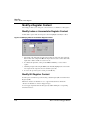
How to Contact Us
Corporate Headquarters
Freescale Semiconductor, Inc.
7700 West Parmer Lane
Austin, TX 78729
U.S.A.
World Wide Web
http://www.freescale.com/codewarrior
Technical Support
http://www.freescale.com/support
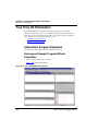
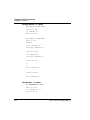
Table of Contents
Introduction
Manual Contents . . . . . . . . . . . . . . . . . . . . . . . . . . . . . . . . . . . . . . . . . . . . . . . . . 21
Book I - Debugger Engine
Book I Contents . . . . . . . . . . . . . . . . . . . . . . . . . . . . . . . . . . . . . . . . . . . . . . . . . 23
1
Introduction
25
Freescale Debugger. . . . . . . . . . . . . . . . . . . . . . . . . . . . . . . . . . . . . . . . . . . . . . . 25
Debugger Application . . . . . . . . . . . . . . . . . . . . . . . . . . . . . . . . . . . . . . . . . . . . . 25
Debugger Features . . . . . . . . . . . . . . . . . . . . . . . . . . . . . . . . . . . . . . . . . . . . . . . 26
Demo Version Limitations on Components . . . . . . . . . . . . . . . . . . . . . . . . . 26
2
Debugger Interface
27
Introduction. . . . . . . . . . . . . . . . . . . . . . . . . . . . . . . . . . . . . . . . . . . . . . . . . . . . . 27
Application Programs . . . . . . . . . . . . . . . . . . . . . . . . . . . . . . . . . . . . . . . . . . . . . 27
Starting the Debugger . . . . . . . . . . . . . . . . . . . . . . . . . . . . . . . . . . . . . . . . . . . . . 28
Starting from within the IDE. . . . . . . . . . . . . . . . . . . . . . . . . . . . . . . . . . . . . 28
Debugger Command Line Start. . . . . . . . . . . . . . . . . . . . . . . . . . . . . . . . . . . 29
Debugger Main Window. . . . . . . . . . . . . . . . . . . . . . . . . . . . . . . . . . . . . . . . . . . 32
Debugger Main Window Toolbar . . . . . . . . . . . . . . . . . . . . . . . . . . . . . . . . . 33
Debugger Main Window Status Bar . . . . . . . . . . . . . . . . . . . . . . . . . . . . . . . 33
Main Window Menu Bar. . . . . . . . . . . . . . . . . . . . . . . . . . . . . . . . . . . . . . . . 33
Component Menu . . . . . . . . . . . . . . . . . . . . . . . . . . . . . . . . . . . . . . . . . . . . . 47
Window Menu . . . . . . . . . . . . . . . . . . . . . . . . . . . . . . . . . . . . . . . . . . . . . . . . 50
Help Menu. . . . . . . . . . . . . . . . . . . . . . . . . . . . . . . . . . . . . . . . . . . . . . . . . . . 51
Component Associated Menus . . . . . . . . . . . . . . . . . . . . . . . . . . . . . . . . . . . . . . 52
Component Main Menu . . . . . . . . . . . . . . . . . . . . . . . . . . . . . . . . . . . . . . . . 52
Microcontrollers Debugger Manual
3
Table of Contents
Component Windows Object Info Bar . . . . . . . . . . . . . . . . . . . . . . . . . . . . .53
Component Context Menu. . . . . . . . . . . . . . . . . . . . . . . . . . . . . . . . . . . . . . .53
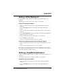
Highlights of the User Interface . . . . . . . . . . . . . . . . . . . . . . . . . . . . . . . . . . . . .54
Activating Services with Drag and Drop. . . . . . . . . . . . . . . . . . . . . . . . . . . .54
To Drag and Drop an Object . . . . . . . . . . . . . . . . . . . . . . . . . . . . . . . . . . . . .55
Drag and Drop Combinations . . . . . . . . . . . . . . . . . . . . . . . . . . . . . . . . . . . .55
3
Debugger Components
61
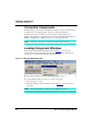
Component Introduction . . . . . . . . . . . . . . . . . . . . . . . . . . . . . . . . . . . . . . . . . . .61
CPU Components . . . . . . . . . . . . . . . . . . . . . . . . . . . . . . . . . . . . . . . . . . . . .61
Window Components. . . . . . . . . . . . . . . . . . . . . . . . . . . . . . . . . . . . . . . . . . .61
Connection Components . . . . . . . . . . . . . . . . . . . . . . . . . . . . . . . . . . . . . . . .62
Loading Component Windows . . . . . . . . . . . . . . . . . . . . . . . . . . . . . . . . . . .62
General Debugger Components . . . . . . . . . . . . . . . . . . . . . . . . . . . . . . . . . . . . .64
Assembly Component . . . . . . . . . . . . . . . . . . . . . . . . . . . . . . . . . . . . . . . . . .64
Command Line Component. . . . . . . . . . . . . . . . . . . . . . . . . . . . . . . . . . . . . .69
Coverage Component . . . . . . . . . . . . . . . . . . . . . . . . . . . . . . . . . . . . . . . . . .73
DA-C Link Component . . . . . . . . . . . . . . . . . . . . . . . . . . . . . . . . . . . . . . . . .76
Data Component . . . . . . . . . . . . . . . . . . . . . . . . . . . . . . . . . . . . . . . . . . . . . .79
Memory Component . . . . . . . . . . . . . . . . . . . . . . . . . . . . . . . . . . . . . . . . . . .90
Module Component . . . . . . . . . . . . . . . . . . . . . . . . . . . . . . . . . . . . . . . . . . .102
Procedure Component . . . . . . . . . . . . . . . . . . . . . . . . . . . . . . . . . . . . . . . . .104
Profiler Component . . . . . . . . . . . . . . . . . . . . . . . . . . . . . . . . . . . . . . . . . . .106
Recorder Component . . . . . . . . . . . . . . . . . . . . . . . . . . . . . . . . . . . . . . . . . .109
Register Component . . . . . . . . . . . . . . . . . . . . . . . . . . . . . . . . . . . . . . . . . .111
Source Component . . . . . . . . . . . . . . . . . . . . . . . . . . . . . . . . . . . . . . . . . . .115
Terminal Component . . . . . . . . . . . . . . . . . . . . . . . . . . . . . . . . . . . . . . . . . .125
Trace Component. . . . . . . . . . . . . . . . . . . . . . . . . . . . . . . . . . . . . . . . . . . . .130
Visualization Utilities . . . . . . . . . . . . . . . . . . . . . . . . . . . . . . . . . . . . . . . . . . . .133
Inspector Component. . . . . . . . . . . . . . . . . . . . . . . . . . . . . . . . . . . . . . . . . .133
Visualization Tool Component . . . . . . . . . . . . . . . . . . . . . . . . . . . . . . . . . .141
4
Control Points
157
Introduction . . . . . . . . . . . . . . . . . . . . . . . . . . . . . . . . . . . . . . . . . . . . . . . . . . . .157
Breakpoints . . . . . . . . . . . . . . . . . . . . . . . . . . . . . . . . . . . . . . . . . . . . . . . . . . . .158
4
Microcontrollers Debugger Manual
Table of Contents
Breakpoints Tab. . . . . . . . . . . . . . . . . . . . . . . . . . . . . . . . . . . . . . . . . . . . . . 160
Multiple Selections in List Box. . . . . . . . . . . . . . . . . . . . . . . . . . . . . . . . . . 161
Checking Expressions . . . . . . . . . . . . . . . . . . . . . . . . . . . . . . . . . . . . . . . . . 161
Saving Breakpoints . . . . . . . . . . . . . . . . . . . . . . . . . . . . . . . . . . . . . . . . . . . 162
Setting Breakpoints. . . . . . . . . . . . . . . . . . . . . . . . . . . . . . . . . . . . . . . . . . . . . . 164
Positions Where a Breakpoint Is Definable . . . . . . . . . . . . . . . . . . . . . . . . 164
Temporary Breakpoints . . . . . . . . . . . . . . . . . . . . . . . . . . . . . . . . . . . . . . . . 165
Permanent Breakpoints . . . . . . . . . . . . . . . . . . . . . . . . . . . . . . . . . . . . . . . . 165
Counting Breakpoints . . . . . . . . . . . . . . . . . . . . . . . . . . . . . . . . . . . . . . . . . 166
Conditional Breakpoints . . . . . . . . . . . . . . . . . . . . . . . . . . . . . . . . . . . . . . . 167
Deleting Breakpoints. . . . . . . . . . . . . . . . . . . . . . . . . . . . . . . . . . . . . . . . . . 168
Associate a Command with a Breakpoint . . . . . . . . . . . . . . . . . . . . . . . . . . 169
Watchpoints. . . . . . . . . . . . . . . . . . . . . . . . . . . . . . . . . . . . . . . . . . . . . . . . . . . . 170
Watchpoints Tab . . . . . . . . . . . . . . . . . . . . . . . . . . . . . . . . . . . . . . . . . . . . . 172
Multiple Selections . . . . . . . . . . . . . . . . . . . . . . . . . . . . . . . . . . . . . . . . . . . 173
Checking Syntax . . . . . . . . . . . . . . . . . . . . . . . . . . . . . . . . . . . . . . . . . . . . . 173
Setting Watchpoints . . . . . . . . . . . . . . . . . . . . . . . . . . . . . . . . . . . . . . . . . . . . . 174
Setting a Read Watchpoint . . . . . . . . . . . . . . . . . . . . . . . . . . . . . . . . . . . . . 174
Setting a Write Watchpoint . . . . . . . . . . . . . . . . . . . . . . . . . . . . . . . . . . . . . 175
Defining a Read/Write Watchpoint . . . . . . . . . . . . . . . . . . . . . . . . . . . . . . . 175
Defining a Counting Watchpoint. . . . . . . . . . . . . . . . . . . . . . . . . . . . . . . . . 176
Defining a Conditional Watchpoint. . . . . . . . . . . . . . . . . . . . . . . . . . . . . . . 177
Deleting a Watchpoint . . . . . . . . . . . . . . . . . . . . . . . . . . . . . . . . . . . . . . . . . 178
Associate a Command with a Watchpoint. . . . . . . . . . . . . . . . . . . . . . . . . . 178
Markpoints . . . . . . . . . . . . . . . . . . . . . . . . . . . . . . . . . . . . . . . . . . . . . . . . . . . . 179
Markpoints Tab . . . . . . . . . . . . . . . . . . . . . . . . . . . . . . . . . . . . . . . . . . . . . . 181
Setting Markpoints . . . . . . . . . . . . . . . . . . . . . . . . . . . . . . . . . . . . . . . . . . . . . . 182
Setting a Source Markpoint . . . . . . . . . . . . . . . . . . . . . . . . . . . . . . . . . . . . 182
Setting a Data Markpoint . . . . . . . . . . . . . . . . . . . . . . . . . . . . . . . . . . . . . . 183
Setting a Memory Markpoint . . . . . . . . . . . . . . . . . . . . . . . . . . . . . . . . . . . 183
Deleting a Markpoint . . . . . . . . . . . . . . . . . . . . . . . . . . . . . . . . . . . . . . . . . 184
Halting on a Control Point . . . . . . . . . . . . . . . . . . . . . . . . . . . . . . . . . . . . . . . . 184
5
Real Time Kernel Awareness
185
Introduction. . . . . . . . . . . . . . . . . . . . . . . . . . . . . . . . . . . . . . . . . . . . . . . . . . . . 185
Microcontrollers Debugger Manual
5
Table of Contents
Inspecting Task State . . . . . . . . . . . . . . . . . . . . . . . . . . . . . . . . . . . . . . . . . .186
Task Description Language . . . . . . . . . . . . . . . . . . . . . . . . . . . . . . . . . . . . . . . .186
Application Example. . . . . . . . . . . . . . . . . . . . . . . . . . . . . . . . . . . . . . . . . . . . .188
Inspecting Kernel Data Structures. . . . . . . . . . . . . . . . . . . . . . . . . . . . . . . . . . .189
OSEK Kernel Awareness. . . . . . . . . . . . . . . . . . . . . . . . . . . . . . . . . . . . . . . . . .190
OSEK Run Time Interface. . . . . . . . . . . . . . . . . . . . . . . . . . . . . . . . . . . . . .191
ORTI File and Filename . . . . . . . . . . . . . . . . . . . . . . . . . . . . . . . . . . . . . . .191
OSEK RTK Inspector Component. . . . . . . . . . . . . . . . . . . . . . . . . . . . . . . .193
6
How To...
199
How To Configure the Debugger . . . . . . . . . . . . . . . . . . . . . . . . . . . . . . . . . . .199
For Use from Desktop . . . . . . . . . . . . . . . . . . . . . . . . . . . . . . . . . . . . . . . . .199
Starting Debugger from CodeWarrior IDE . . . . . . . . . . . . . . . . . . . . . . . . . . . .200
Automating Debugger Startup. . . . . . . . . . . . . . . . . . . . . . . . . . . . . . . . . . . . . .201
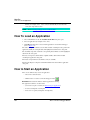
How To Load an Application . . . . . . . . . . . . . . . . . . . . . . . . . . . . . . . . . . . . . .202
How to Start an Application . . . . . . . . . . . . . . . . . . . . . . . . . . . . . . . . . . . . . . .202
How to Stop an Application . . . . . . . . . . . . . . . . . . . . . . . . . . . . . . . . . . . . . . .203
How to Step in the Application . . . . . . . . . . . . . . . . . . . . . . . . . . . . . . . . . . . . .203
On Source Level . . . . . . . . . . . . . . . . . . . . . . . . . . . . . . . . . . . . . . . . . . . . .203
Step Over a Function Call (Flat Step) . . . . . . . . . . . . . . . . . . . . . . . . . . . . .204
Step on Assembly Level . . . . . . . . . . . . . . . . . . . . . . . . . . . . . . . . . . . . . . .205
How to Work on Variables . . . . . . . . . . . . . . . . . . . . . . . . . . . . . . . . . . . . . . . .205
Display Local Variable from a Function . . . . . . . . . . . . . . . . . . . . . . . . . . .205
Display Global Variable from a Module . . . . . . . . . . . . . . . . . . . . . . . . . . .206
Change Format for Variable Value Display . . . . . . . . . . . . . . . . . . . . . . . . .207
Modify a Variable Value . . . . . . . . . . . . . . . . . . . . . . . . . . . . . . . . . . . . . . .208
Get the Address Where a Variable is Allocated. . . . . . . . . . . . . . . . . . . . . .208
Inspect Memory Starting at a Variable Location Address . . . . . . . . . . . . . .209
Load an Address Register with the Address of a Variable . . . . . . . . . . . . .209
How to Work on the Register . . . . . . . . . . . . . . . . . . . . . . . . . . . . . . . . . . . . . .209
Change Format of Register Display. . . . . . . . . . . . . . . . . . . . . . . . . . . . . . .209
Modify a Register Content. . . . . . . . . . . . . . . . . . . . . . . . . . . . . . . . . . . . . .210
Start Memory Dump at Address Where Register is Pointing . . . . . . . . . . .211
Modify Content of Memory Address . . . . . . . . . . . . . . . . . . . . . . . . . . . . . . . .212
How to Consult Assembler Instructions Generated by a Source Statement . . .212
6
Microcontrollers Debugger Manual
Table of Contents
How to View Code . . . . . . . . . . . . . . . . . . . . . . . . . . . . . . . . . . . . . . . . . . . . . . 213
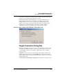
How to Communicate with the Application . . . . . . . . . . . . . . . . . . . . . . . . . . . 214
7
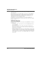
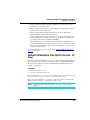
CodeWarrior IDE Integration
215
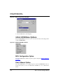
Debugger Configuration . . . . . . . . . . . . . . . . . . . . . . . . . . . . . . . . . . . . . . . . . . 215
8
Debugger DDE Capabilities
217
Introduction . . . . . . . . . . . . . . . . . . . . . . . . . . . . . . . . . . . . . . . . . . . . . . . . . 217
DDE Implementation . . . . . . . . . . . . . . . . . . . . . . . . . . . . . . . . . . . . . . . . . 217
9
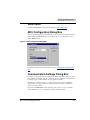
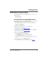
Synchronized Debugging Through DA-C IDE
219
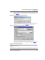
Configuring DA-C IDE for Freescale Tool Kit. . . . . . . . . . . . . . . . . . . . . . . . . 219
Create New Project . . . . . . . . . . . . . . . . . . . . . . . . . . . . . . . . . . . . . . . . . . . 220
Configuring The Tools . . . . . . . . . . . . . . . . . . . . . . . . . . . . . . . . . . . . . . . . 226
Debugger Interface . . . . . . . . . . . . . . . . . . . . . . . . . . . . . . . . . . . . . . . . . . . . . . 230
DA-C IDE and Debugger Communication . . . . . . . . . . . . . . . . . . . . . . . . . 230
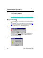
Synchronized Debugging . . . . . . . . . . . . . . . . . . . . . . . . . . . . . . . . . . . . . . . . . 233
Troubleshooting . . . . . . . . . . . . . . . . . . . . . . . . . . . . . . . . . . . . . . . . . . . . . . . . 234
Book II - HC08 Debug Connections
Book II Contents . . . . . . . . . . . . . . . . . . . . . . . . . . . . . . . . . . . . . . . . . . . . . . . . 237
10 Microcontroller Debugging First Steps
239
Technical Considerations . . . . . . . . . . . . . . . . . . . . . . . . . . . . . . . . . . . . . . . . . 239
Full Chip Simulation Considerations . . . . . . . . . . . . . . . . . . . . . . . . . . . . . 239
HC08 Serial Monitor Considerations . . . . . . . . . . . . . . . . . . . . . . . . . . . . . 240
ICS MON08 Interface Connection . . . . . . . . . . . . . . . . . . . . . . . . . . . . . . . 240
P&E Multilink/Cyclone Pro Considerations . . . . . . . . . . . . . . . . . . . . . . . . 240
ICS P&E Multilink/Cyclone Pro Considerations . . . . . . . . . . . . . . . . . . . . 240
SofTec HC08 Considerations . . . . . . . . . . . . . . . . . . . . . . . . . . . . . . . . . . . 240
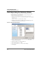
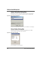
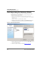
Debugging First Steps Using the Wizard . . . . . . . . . . . . . . . . . . . . . . . . . . . . . 241
Switching Connections . . . . . . . . . . . . . . . . . . . . . . . . . . . . . . . . . . . . . . . . . . . 246
Microcontrollers Debugger Manual
7
Table of Contents
Loading the Full Chip Simulation Connection . . . . . . . . . . . . . . . . . . . . . .246
Loading the P&E Multilink/Cyclone Pro Connection. . . . . . . . . . . . . . . . .248
Loading the HC(S)08 or RS08 Open Source BDM Connection . . . . . . . . .251
11 HC08 Full Chip Simulation
253
Configuration Procedure . . . . . . . . . . . . . . . . . . . . . . . . . . . . . . . . . . . . . . . . . .253
Select Device Option . . . . . . . . . . . . . . . . . . . . . . . . . . . . . . . . . . . . . . . . . .255
Full Chip Simulation Module Commands. . . . . . . . . . . . . . . . . . . . . . . . . .255
Peripheral Modules Options . . . . . . . . . . . . . . . . . . . . . . . . . . . . . . . . . . . .257
ADC Module Option . . . . . . . . . . . . . . . . . . . . . . . . . . . . . . . . . . . . . . . . . .258
Clock Generation Module Option . . . . . . . . . . . . . . . . . . . . . . . . . . . . . . . .260
High-Resolution PWM Module. . . . . . . . . . . . . . . . . . . . . . . . . . . . . . . . . .262
Input/Output (I/O) Ports Module . . . . . . . . . . . . . . . . . . . . . . . . . . . . . . . . .265
External Interrupt Module . . . . . . . . . . . . . . . . . . . . . . . . . . . . . . . . . . . . . .268
Keyboard Interrupt Module . . . . . . . . . . . . . . . . . . . . . . . . . . . . . . . . . . . . .269
Multi-Master Inter-Integrated Circuit Module . . . . . . . . . . . . . . . . . . . . . .272
FCSMSCAN Controller Module . . . . . . . . . . . . . . . . . . . . . . . . . . . . . . . . .276
FCS Programmable Timer Interrupt Module. . . . . . . . . . . . . . . . . . . . . . . .291
FCS Serial Communications Interface Module. . . . . . . . . . . . . . . . . . . . . .292
FCS Slave LIN Interface Controller Module. . . . . . . . . . . . . . . . . . . . . . . .296
FCS Serial Peripheral Interface Module . . . . . . . . . . . . . . . . . . . . . . . . . . .300
FCSTimer Interface Module . . . . . . . . . . . . . . . . . . . . . . . . . . . . . . . . . . . .304
FCS Universal Serial Bus (USB) Module . . . . . . . . . . . . . . . . . . . . . . . . . .309
12 MON08 Interface Connection
333
Connection Procedure . . . . . . . . . . . . . . . . . . . . . . . . . . . . . . . . . . . . . . . . . . . .333
Advanced Settings Tab . . . . . . . . . . . . . . . . . . . . . . . . . . . . . . . . . . . . . . . .335
Target MCU Security Bytes. . . . . . . . . . . . . . . . . . . . . . . . . . . . . . . . . . . . .338
Active Mode Connection Menu Options . . . . . . . . . . . . . . . . . . . . . . . . . . .342
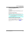
Device Class Description . . . . . . . . . . . . . . . . . . . . . . . . . . . . . . . . . . . . . . . . .346
13 ICS MON08 Interface Connection
349
ICS Mode . . . . . . . . . . . . . . . . . . . . . . . . . . . . . . . . . . . . . . . . . . . . . . . . . . . . .349
Connection Procedure . . . . . . . . . . . . . . . . . . . . . . . . . . . . . . . . . . . . . . . . . . . .350
Advanced Settings Tab . . . . . . . . . . . . . . . . . . . . . . . . . . . . . . . . . . . . . . . .352
8
Microcontrollers Debugger Manual
Table of Contents
Cycle Power Radio Button . . . . . . . . . . . . . . . . . . . . . . . . . . . . . . . . . . . . . 354
Target MCU Security Bytes . . . . . . . . . . . . . . . . . . . . . . . . . . . . . . . . . . . . 355
STATUS Area . . . . . . . . . . . . . . . . . . . . . . . . . . . . . . . . . . . . . . . . . . . . . . . 355
Active Mode Connection Menu Options. . . . . . . . . . . . . . . . . . . . . . . . . . . 358
Device Class Description . . . . . . . . . . . . . . . . . . . . . . . . . . . . . . . . . . . . . . . . . 361
14 HC08 P&E Multilink/Cyclone Pro Connection
365
Connection Procedure. . . . . . . . . . . . . . . . . . . . . . . . . . . . . . . . . . . . . . . . . . . . 365
Advanced Settings Tab . . . . . . . . . . . . . . . . . . . . . . . . . . . . . . . . . . . . . . . . 368
Target MCU Security Bytes . . . . . . . . . . . . . . . . . . . . . . . . . . . . . . . . . . . . 371
STATUS Area . . . . . . . . . . . . . . . . . . . . . . . . . . . . . . . . . . . . . . . . . . . . . . . 372
Connection (MultilinkCyclonePro) Menu . . . . . . . . . . . . . . . . . . . . . . . . . 374
Active Mode Menu Options . . . . . . . . . . . . . . . . . . . . . . . . . . . . . . . . . . . . 375
Debugging Limitations . . . . . . . . . . . . . . . . . . . . . . . . . . . . . . . . . . . . . . . . 379
Debugging Tips . . . . . . . . . . . . . . . . . . . . . . . . . . . . . . . . . . . . . . . . . . . . . . 379
Device Class Description . . . . . . . . . . . . . . . . . . . . . . . . . . . . . . . . . . . . . . . . . 380
Class 5 Device . . . . . . . . . . . . . . . . . . . . . . . . . . . . . . . . . . . . . . . . . . . . . . . 380
Class 7 Device . . . . . . . . . . . . . . . . . . . . . . . . . . . . . . . . . . . . . . . . . . . . . . . 380
Class 8 Device . . . . . . . . . . . . . . . . . . . . . . . . . . . . . . . . . . . . . . . . . . . . . . . 380
15 HC08 ICS P&E Multilink/Cyclone Pro Connections
381
Connection Procedure. . . . . . . . . . . . . . . . . . . . . . . . . . . . . . . . . . . . . . . . . . . . 382
Advanced Settings Tab . . . . . . . . . . . . . . . . . . . . . . . . . . . . . . . . . . . . . . . . 384
Target MCU Security Bytes . . . . . . . . . . . . . . . . . . . . . . . . . . . . . . . . . . . . 387
STATUS Area . . . . . . . . . . . . . . . . . . . . . . . . . . . . . . . . . . . . . . . . . . . . . . . 387
Active Mode Menu Options . . . . . . . . . . . . . . . . . . . . . . . . . . . . . . . . . . . . 390
Device Class Description . . . . . . . . . . . . . . . . . . . . . . . . . . . . . . . . . . . . . . . . . 393
Class 5 Device . . . . . . . . . . . . . . . . . . . . . . . . . . . . . . . . . . . . . . . . . . . . . . . 393
Class 7 Device . . . . . . . . . . . . . . . . . . . . . . . . . . . . . . . . . . . . . . . . . . . . . . . 393
Class 8 Device . . . . . . . . . . . . . . . . . . . . . . . . . . . . . . . . . . . . . . . . . . . . . . . 394
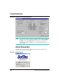
16 SofTec HC08 Connection
395
SofTec HC08 Technical Considerations . . . . . . . . . . . . . . . . . . . . . . . . . . . . . . 395
CodeWarrior IDE and SofTec HC08 Connection . . . . . . . . . . . . . . . . . . . . . . . 395
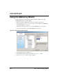
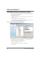
Using the Stationery Wizard . . . . . . . . . . . . . . . . . . . . . . . . . . . . . . . . . . . . . . . 396
Microcontrollers Debugger Manual
9
Table of Contents
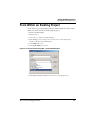
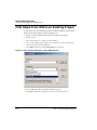
From Within an Existing Project. . . . . . . . . . . . . . . . . . . . . . . . . . . . . . . . . . . .397
inDart-HC08 Menu Options . . . . . . . . . . . . . . . . . . . . . . . . . . . . . . . . . . . .398
MCU Configuration Dialog Box . . . . . . . . . . . . . . . . . . . . . . . . . . . . . . . . .399
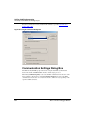
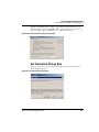
Communication Settings Dialog Box . . . . . . . . . . . . . . . . . . . . . . . . . . . . .399
About Dialog Box . . . . . . . . . . . . . . . . . . . . . . . . . . . . . . . . . . . . . . . . . . . .400
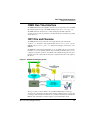
17 HC08 FSICEBASE Emulator
401
FSICEBASE Overview . . . . . . . . . . . . . . . . . . . . . . . . . . . . . . . . . . . . . . . . . . .401
System Requirements . . . . . . . . . . . . . . . . . . . . . . . . . . . . . . . . . . . . . . . . .402
System Features . . . . . . . . . . . . . . . . . . . . . . . . . . . . . . . . . . . . . . . . . . . . . .402
System Components . . . . . . . . . . . . . . . . . . . . . . . . . . . . . . . . . . . . . . . . . .403
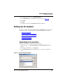
Setting Up the FSICEBASE System . . . . . . . . . . . . . . . . . . . . . . . . . . . . . . . . .405
Setting Up the Hardware . . . . . . . . . . . . . . . . . . . . . . . . . . . . . . . . . . . . . . .405
Establishing Communication . . . . . . . . . . . . . . . . . . . . . . . . . . . . . . . . . . . . . .407
Communication Through Ethernet Port . . . . . . . . . . . . . . . . . . . . . . . . . . .407
Communication Through USB Port . . . . . . . . . . . . . . . . . . . . . . . . . . . . . .408
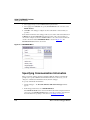
Setting Up the System . . . . . . . . . . . . . . . . . . . . . . . . . . . . . . . . . . . . . . . . . . . .409
Specifying A Connection. . . . . . . . . . . . . . . . . . . . . . . . . . . . . . . . . . . . . . .409
Specifying Communication Information . . . . . . . . . . . . . . . . . . . . . . . . . . .410
Assigning an IP Address to FSICEBASE . . . . . . . . . . . . . . . . . . . . . . . . . .412
Specifying a Memory Map . . . . . . . . . . . . . . . . . . . . . . . . . . . . . . . . . . . . . . . .414
Specifying the Clock Speed. . . . . . . . . . . . . . . . . . . . . . . . . . . . . . . . . . . . .417
Emulation System Reset . . . . . . . . . . . . . . . . . . . . . . . . . . . . . . . . . . . . . . .419
Setting Up Logic Cables and Connectors . . . . . . . . . . . . . . . . . . . . . . . . . . . . .419
Bus State Analyzer (BSA). . . . . . . . . . . . . . . . . . . . . . . . . . . . . . . . . . . . . . . . .421
Using BSA . . . . . . . . . . . . . . . . . . . . . . . . . . . . . . . . . . . . . . . . . . . . . . . . . .421
Book III - HCS08 Debug Connections
Book III Contents . . . . . . . . . . . . . . . . . . . . . . . . . . . . . . . . . . . . . . . . . . . . . . .429
18 HCS08 Full Chip Simulation
431
Configuration Procedure . . . . . . . . . . . . . . . . . . . . . . . . . . . . . . . . . . . . . . . . . .431
10
Microcontrollers Debugger Manual
Table of Contents
Connection (HCS08FCS) Menu . . . . . . . . . . . . . . . . . . . . . . . . . . . . . . . . . 432
Peripheral Modules Commands . . . . . . . . . . . . . . . . . . . . . . . . . . . . . . . . . . . . 435
ADC Module . . . . . . . . . . . . . . . . . . . . . . . . . . . . . . . . . . . . . . . . . . . . . . . . 436
Clock Generation Module . . . . . . . . . . . . . . . . . . . . . . . . . . . . . . . . . . . . . . 438
Inter-Integrated Circuit Module . . . . . . . . . . . . . . . . . . . . . . . . . . . . . . . . . 440
Input/Output (I/O) Ports Module. . . . . . . . . . . . . . . . . . . . . . . . . . . . . . . . . 444
External Interrupt (IRQ) Module . . . . . . . . . . . . . . . . . . . . . . . . . . . . . . . . 447
Keyboard Interrupt Module. . . . . . . . . . . . . . . . . . . . . . . . . . . . . . . . . . . . . 450
Modulo Timer Interrupt Module . . . . . . . . . . . . . . . . . . . . . . . . . . . . . . . . . 452
Serial Communications Interface Module. . . . . . . . . . . . . . . . . . . . . . . . . . 453
Serial Peripheral Interface Module . . . . . . . . . . . . . . . . . . . . . . . . . . . . . . . 457
Timer Interface Module. . . . . . . . . . . . . . . . . . . . . . . . . . . . . . . . . . . . . . . . 461
19 HCS08 P&E Multilink/Cyclone Pro Connection
467
Connection Procedure. . . . . . . . . . . . . . . . . . . . . . . . . . . . . . . . . . . . . . . . . . . . 467
MultilinkCyclonePro Menu Description. . . . . . . . . . . . . . . . . . . . . . . . . . . 470
Active Mode Menu Options . . . . . . . . . . . . . . . . . . . . . . . . . . . . . . . . . . . . 471
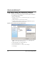
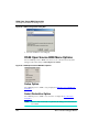
20 HCS08 Open Source BDM Connection
477
HCS08 Open Source BDM Technical Considerations . . . . . . . . . . . . . . . . . . . 477
CodeWarrior IDE and HCS08 Open Source BDM Connection . . . . . . . . . . . . 477
First Steps Using the Stationery Wizard . . . . . . . . . . . . . . . . . . . . . . . . . . . . . . 478
First Steps From Within an Existing Project . . . . . . . . . . . . . . . . . . . . . . . . . . 479
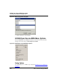
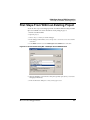
HCS08 Open Source BDM Menu Options . . . . . . . . . . . . . . . . . . . . . . . . . 480
HCS08 Open Source BDM Setup Dialog Box . . . . . . . . . . . . . . . . . . . . . . 482
Select Derivative Dialog Box . . . . . . . . . . . . . . . . . . . . . . . . . . . . . . . . . . . 483
Information Required to Unsecure the Device . . . . . . . . . . . . . . . . . . . . . . 484
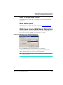
Show Status Dialog Box . . . . . . . . . . . . . . . . . . . . . . . . . . . . . . . . . . . . . . . 485
21 HCS08 Serial Monitor Connection
487
Serial Monitor Technical Considerations . . . . . . . . . . . . . . . . . . . . . . . . . . . . . 487
CodeWarrior IDE and Serial Monitor Connection . . . . . . . . . . . . . . . . . . . . . . 487
First Steps Using the Stationery Wizard . . . . . . . . . . . . . . . . . . . . . . . . . . . . . . 488
First Steps from Within an Existing Project . . . . . . . . . . . . . . . . . . . . . . . . . . . 489
MONITOR-HCS08 Menu Options . . . . . . . . . . . . . . . . . . . . . . . . . . . . . . . 492
Microcontrollers Debugger Manual
11
Table of Contents
Monitor Setup Window . . . . . . . . . . . . . . . . . . . . . . . . . . . . . . . . . . . . . . . .493
Derivative Selection Dialog Box . . . . . . . . . . . . . . . . . . . . . . . . . . . . . . . . .495
22 SofTec HCS08 Connection
497
SofTec HCS08 Technical Considerations . . . . . . . . . . . . . . . . . . . . . . . . . . . . .497
CodeWarrior IDE and SofTec HCS08 Connection . . . . . . . . . . . . . . . . . . . . . .497
First Steps Using the Stationery Wizard . . . . . . . . . . . . . . . . . . . . . . . . . . . . . .498
First Steps from Within an Existing Project . . . . . . . . . . . . . . . . . . . . . . . . . . .499
SofTec HCS08 Menu Options . . . . . . . . . . . . . . . . . . . . . . . . . . . . . . . . . . .500
MCU Configuration Dialog Box . . . . . . . . . . . . . . . . . . . . . . . . . . . . . . . . .501
Communication Settings Dialog Box . . . . . . . . . . . . . . . . . . . . . . . . . . . . .501
About Dialog Box . . . . . . . . . . . . . . . . . . . . . . . . . . . . . . . . . . . . . . . . . . . .502
23 HCS08 On-Chip DBG Module
503
Reference Document . . . . . . . . . . . . . . . . . . . . . . . . . . . . . . . . . . . . . . . . . . . . .503
DBG Features . . . . . . . . . . . . . . . . . . . . . . . . . . . . . . . . . . . . . . . . . . . . . . . . . .503
Specific Connection Menu Options . . . . . . . . . . . . . . . . . . . . . . . . . . . . . . . . .504
Context Menu Entries in Source, Data, Assembly and Memory Windows . . .505
Source and Assembly Windows . . . . . . . . . . . . . . . . . . . . . . . . . . . . . . . . .505
Trigger Stored as Markpoints . . . . . . . . . . . . . . . . . . . . . . . . . . . . . . . . . . .508
Data and Memory Windows . . . . . . . . . . . . . . . . . . . . . . . . . . . . . . . . . . . .509
Expert Triggers . . . . . . . . . . . . . . . . . . . . . . . . . . . . . . . . . . . . . . . . . . . . . .512
Trigger Settings . . . . . . . . . . . . . . . . . . . . . . . . . . . . . . . . . . . . . . . . . . . . . .514
Trigger Module Usage . . . . . . . . . . . . . . . . . . . . . . . . . . . . . . . . . . . . . . . . .515
DBG Support Status Bar Item . . . . . . . . . . . . . . . . . . . . . . . . . . . . . . . . . . . . . .515
Trigger Module Settings Window . . . . . . . . . . . . . . . . . . . . . . . . . . . . . . . . . . .516
DBG Module Mode Setup . . . . . . . . . . . . . . . . . . . . . . . . . . . . . . . . . . . . . .517
Automatic Mode (Default) . . . . . . . . . . . . . . . . . . . . . . . . . . . . . . . . . . . . .517
Expert Mode . . . . . . . . . . . . . . . . . . . . . . . . . . . . . . . . . . . . . . . . . . . . . . . .518
Expert Mode Tab . . . . . . . . . . . . . . . . . . . . . . . . . . . . . . . . . . . . . . . . . . . . .519
Profiling and Coverage Mode . . . . . . . . . . . . . . . . . . . . . . . . . . . . . . . . . . .519
Disabled Mode. . . . . . . . . . . . . . . . . . . . . . . . . . . . . . . . . . . . . . . . . . . . . . .520
Memory Access Triggers. . . . . . . . . . . . . . . . . . . . . . . . . . . . . . . . . . . . . . .521
Instruction Triggers . . . . . . . . . . . . . . . . . . . . . . . . . . . . . . . . . . . . . . . . . . .523
Capture Triggers . . . . . . . . . . . . . . . . . . . . . . . . . . . . . . . . . . . . . . . . . . . . .526
12
Microcontrollers Debugger Manual
Table of Contents
DBG Module Options . . . . . . . . . . . . . . . . . . . . . . . . . . . . . . . . . . . . . . . . . 527
Trigger Editing . . . . . . . . . . . . . . . . . . . . . . . . . . . . . . . . . . . . . . . . . . . . . . 529
Trigger Module Settings Window - Display Information . . . . . . . . . . . . . . 530
General Settings Tab . . . . . . . . . . . . . . . . . . . . . . . . . . . . . . . . . . . . . . . . . . 531
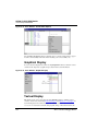
Trace Component Window . . . . . . . . . . . . . . . . . . . . . . . . . . . . . . . . . . . . . . . . 532
Instructions Display. . . . . . . . . . . . . . . . . . . . . . . . . . . . . . . . . . . . . . . . . . . 533
Graphical Display . . . . . . . . . . . . . . . . . . . . . . . . . . . . . . . . . . . . . . . . . . . . 534
Textual Display . . . . . . . . . . . . . . . . . . . . . . . . . . . . . . . . . . . . . . . . . . . . . . 534
Column Display and Moving . . . . . . . . . . . . . . . . . . . . . . . . . . . . . . . . . . . 535
Goto Frame . . . . . . . . . . . . . . . . . . . . . . . . . . . . . . . . . . . . . . . . . . . . . . . . . 536
Clearing Frames . . . . . . . . . . . . . . . . . . . . . . . . . . . . . . . . . . . . . . . . . . . . . 536
Limitations . . . . . . . . . . . . . . . . . . . . . . . . . . . . . . . . . . . . . . . . . . . . . . . . . . . . 538
HCS08 DBG V3 New Features . . . . . . . . . . . . . . . . . . . . . . . . . . . . . . . . . . . . 538
MMU and Extended Address Space . . . . . . . . . . . . . . . . . . . . . . . . . . . . . . 538
LOOP1 mode. . . . . . . . . . . . . . . . . . . . . . . . . . . . . . . . . . . . . . . . . . . . . . . . 538
Ability to record until Reset and from Reset. . . . . . . . . . . . . . . . . . . . . . . . 539
Expert Triggers tab extended. . . . . . . . . . . . . . . . . . . . . . . . . . . . . . . . . . . . 543
Book IV - RS08 Debug Connections
Book IV Contents . . . . . . . . . . . . . . . . . . . . . . . . . . . . . . . . . . . . . . . . . . . . . . . 545
24 RS08 Full Chip Simulation
547
Configuration Procedure. . . . . . . . . . . . . . . . . . . . . . . . . . . . . . . . . . . . . . . . . . 547
Connection (RS08FCS) Menu . . . . . . . . . . . . . . . . . . . . . . . . . . . . . . . . . . 548
Peripheral Modules Commands . . . . . . . . . . . . . . . . . . . . . . . . . . . . . . . . . . . . 552
25 RS08 P&E Multilink/Cyclone Pro Connection
553
Connection Procedure. . . . . . . . . . . . . . . . . . . . . . . . . . . . . . . . . . . . . . . . . . . . 553
MultilinkCyclonePro Menu Description. . . . . . . . . . . . . . . . . . . . . . . . . . . 555
Active Mode Menu Options . . . . . . . . . . . . . . . . . . . . . . . . . . . . . . . . . . . . 556
Microcontrollers Debugger Manual
13
Table of Contents
26 RS08 Open Source BDM Connection
561
RS08 Open Source BDM Technical Considerations. . . . . . . . . . . . . . . . . . . . .561
CodeWarrior IDE and RS08 Open Source BDM Connection . . . . . . . . . . . . .561
First Steps Using the Stationery Wizard . . . . . . . . . . . . . . . . . . . . . . . . . . . . . .562
First Steps From Within an Existing Project. . . . . . . . . . . . . . . . . . . . . . . . . . .563
RS08 Open Source BDM Menu Options . . . . . . . . . . . . . . . . . . . . . . . . . .564
RS08 Open Source BDM Setup Dialog Box. . . . . . . . . . . . . . . . . . . . . . . .565
Select Derivative Dialog Box . . . . . . . . . . . . . . . . . . . . . . . . . . . . . . . . . . .566
Show Status Dialog Box . . . . . . . . . . . . . . . . . . . . . . . . . . . . . . . . . . . . . . .566
27 SofTec RS08 Connection
567
SofTec RS08 Technical Considerations . . . . . . . . . . . . . . . . . . . . . . . . . . . . . .567
CodeWarrior IDE and SofTec RS08 Connection . . . . . . . . . . . . . . . . . . . . . . .567
First Steps Using the Stationery Wizard . . . . . . . . . . . . . . . . . . . . . . . . . . . . . .568
First Steps From Within an Existing Project. . . . . . . . . . . . . . . . . . . . . . . . . . .570
SofTec RS08 Menu Options . . . . . . . . . . . . . . . . . . . . . . . . . . . . . . . . . . . .571
MCU Configuration Dialog Box . . . . . . . . . . . . . . . . . . . . . . . . . . . . . . . . .572
Communication Settings Dialog Box . . . . . . . . . . . . . . . . . . . . . . . . . . . . .572
About Dialog Box . . . . . . . . . . . . . . . . . . . . . . . . . . . . . . . . . . . . . . . . . . . .573
Book V - ColdFire® V1.0 Debug
Connections
Book V Contents . . . . . . . . . . . . . . . . . . . . . . . . . . . . . . . . . . . . . . . . . . . . . . . .575
28 ColdFire V1 Full Chip Simulation Connection
577
Full Chip Simulation Menu . . . . . . . . . . . . . . . . . . . . . . . . . . . . . . . . . . . . .577
Memory Configuration . . . . . . . . . . . . . . . . . . . . . . . . . . . . . . . . . . . . . . . .580
Clock Frequency Setup . . . . . . . . . . . . . . . . . . . . . . . . . . . . . . . . . . . . . . . .586
Bus Trace . . . . . . . . . . . . . . . . . . . . . . . . . . . . . . . . . . . . . . . . . . . . . . . . . . .587
Full Chip Simulation Warnings . . . . . . . . . . . . . . . . . . . . . . . . . . . . . . . . . .588
FCS and Silicon On-Chip Peripherals Simulation . . . . . . . . . . . . . . . . . . . . . .592
14
Microcontrollers Debugger Manual
Table of Contents
FCS Visualization Utilities . . . . . . . . . . . . . . . . . . . . . . . . . . . . . . . . . . . . . . . . 593
Analog Meter Component. . . . . . . . . . . . . . . . . . . . . . . . . . . . . . . . . . . . . . 594
IO_LED Component . . . . . . . . . . . . . . . . . . . . . . . . . . . . . . . . . . . . . . . . . . 595
LED Component . . . . . . . . . . . . . . . . . . . . . . . . . . . . . . . . . . . . . . . . . . . . . 597
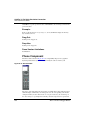
Phone Component . . . . . . . . . . . . . . . . . . . . . . . . . . . . . . . . . . . . . . . . . . . . 598
ADC/DAC Component . . . . . . . . . . . . . . . . . . . . . . . . . . . . . . . . . . . . . . . . 600
Conversion Parameters Dialog Box . . . . . . . . . . . . . . . . . . . . . . . . . . . . . . 603
IT_Keyboard Component . . . . . . . . . . . . . . . . . . . . . . . . . . . . . . . . . . . . . . 605
Interruption Keyboard Setup . . . . . . . . . . . . . . . . . . . . . . . . . . . . . . . . . . . . 607
LCD Component . . . . . . . . . . . . . . . . . . . . . . . . . . . . . . . . . . . . . . . . . . . . . 608
Monitor Component . . . . . . . . . . . . . . . . . . . . . . . . . . . . . . . . . . . . . . . . . . 614
Push Buttons Component . . . . . . . . . . . . . . . . . . . . . . . . . . . . . . . . . . . . . . 617
Programmable IO_Ports Component . . . . . . . . . . . . . . . . . . . . . . . . . . . . . 619
7-Segments Display Component. . . . . . . . . . . . . . . . . . . . . . . . . . . . . . . . . 621
Stimulation Component. . . . . . . . . . . . . . . . . . . . . . . . . . . . . . . . . . . . . . . . 624
Terminal Component. . . . . . . . . . . . . . . . . . . . . . . . . . . . . . . . . . . . . . . . . . 631
True Time I/O Stimulation . . . . . . . . . . . . . . . . . . . . . . . . . . . . . . . . . . . . . . . . 638
Stimulation Program Examples. . . . . . . . . . . . . . . . . . . . . . . . . . . . . . . . . . 638
Stimulation Input File Syntax . . . . . . . . . . . . . . . . . . . . . . . . . . . . . . . . . . . 645
Electrical Signal Generators and Signals Application to Device Pins . . . . . . . 647
Signal IO Component . . . . . . . . . . . . . . . . . . . . . . . . . . . . . . . . . . . . . . . . . 647
Signal Description File EBNF. . . . . . . . . . . . . . . . . . . . . . . . . . . . . . . . . . . 647
Base Signal Files Provided . . . . . . . . . . . . . . . . . . . . . . . . . . . . . . . . . . . . . 652
Virtual Wire Connections with the Pinconn IO Component . . . . . . . . . . . . 652
Command Set to Apply Signal on ATD Pin . . . . . . . . . . . . . . . . . . . . . . . . 654
FCS Tutorials . . . . . . . . . . . . . . . . . . . . . . . . . . . . . . . . . . . . . . . . . . . . . . . . . . 654
Guess the Number . . . . . . . . . . . . . . . . . . . . . . . . . . . . . . . . . . . . . . . . . . . . 654
PWM Sample . . . . . . . . . . . . . . . . . . . . . . . . . . . . . . . . . . . . . . . . . . . . . . . 663
29 ColdFire P&E Multilink/Cyclone Pro Connection
669
P&E Multilink/Cyclone Pro Technical Considerations . . . . . . . . . . . . . . . . . . 669
CodeWarrior IDE and P&E Multilink/Cyclone Pro Connection . . . . . . . . . . . 669
First Steps Using the Stationery Wizard . . . . . . . . . . . . . . . . . . . . . . . . . . . . . . 670
First Steps From Within an Existing Project . . . . . . . . . . . . . . . . . . . . . . . . . . 671
P&E Multilink/Cyclone Pro Menu Options . . . . . . . . . . . . . . . . . . . . . . . . 673
Microcontrollers Debugger Manual
15
Table of Contents
P&E Multilink/Cyclone Pro Setup Dialog Box. . . . . . . . . . . . . . . . . . . . . .674
Connection Manager Dialog Box . . . . . . . . . . . . . . . . . . . . . . . . . . . . . . . .675
Set Derivative Dialog Box . . . . . . . . . . . . . . . . . . . . . . . . . . . . . . . . . . . . . .676
30 SofTec ColdFire Connection
677
SofTec ColdFire Technical Considerations. . . . . . . . . . . . . . . . . . . . . . . . . . . .677
CodeWarrior IDE and SofTec ColdFire Connection. . . . . . . . . . . . . . . . . . . . .677
First Steps Using the Stationery Wizard . . . . . . . . . . . . . . . . . . . . . . . . . . . . . .678
First Steps From Within an Existing Project. . . . . . . . . . . . . . . . . . . . . . . . . . .679
SofTec ColdFire Menu Options. . . . . . . . . . . . . . . . . . . . . . . . . . . . . . . . . .681
SofTec Coldfire Setup Dialog Box . . . . . . . . . . . . . . . . . . . . . . . . . . . . . . .682
Target Connection Dialog Box . . . . . . . . . . . . . . . . . . . . . . . . . . . . . . . . . .683
Communication Settings Dialog Box . . . . . . . . . . . . . . . . . . . . . . . . . . . . .684
Set Derivative Dialog Box . . . . . . . . . . . . . . . . . . . . . . . . . . . . . . . . . . . . . .685
About Dialog Box . . . . . . . . . . . . . . . . . . . . . . . . . . . . . . . . . . . . . . . . . . . .686
31 ColdFire On-Chip DBG Module
687
DBG Features . . . . . . . . . . . . . . . . . . . . . . . . . . . . . . . . . . . . . . . . . . . . . . . . . .687
Context Menu Entries in Source, Data, Assembly and Memory Windows . . .688
Trigger Module Settings Window . . . . . . . . . . . . . . . . . . . . . . . . . . . . . . . . . . .689
Trigger Module Usage/DBG Module Setup . . . . . . . . . . . . . . . . . . . . . . . .689
General Settings. . . . . . . . . . . . . . . . . . . . . . . . . . . . . . . . . . . . . . . . . . . . . .695
Book VI - Connection Common
Features
Book VI Contents . . . . . . . . . . . . . . . . . . . . . . . . . . . . . . . . . . . . . . . . . . . . . . .697
32 Flash Programming
699
Non-Volatile Memory Control Utility Introduction . . . . . . . . . . . . . . . . . . . . .699
Automated Application Programming . . . . . . . . . . . . . . . . . . . . . . . . . . . . . . .699
Setup . . . . . . . . . . . . . . . . . . . . . . . . . . . . . . . . . . . . . . . . . . . . . . . . . . . . . .700
16
Microcontrollers Debugger Manual
Table of Contents
Advanced Options: Erase Prevention . . . . . . . . . . . . . . . . . . . . . . . . . . . . . 701
NVMC Graphical User Interface . . . . . . . . . . . . . . . . . . . . . . . . . . . . . . . . . . . 702
Modules and Module States . . . . . . . . . . . . . . . . . . . . . . . . . . . . . . . . . . . . 702
NVMC Dialog Box . . . . . . . . . . . . . . . . . . . . . . . . . . . . . . . . . . . . . . . . . . . 703
Flash Module Handling. . . . . . . . . . . . . . . . . . . . . . . . . . . . . . . . . . . . . . . . 705
MCU Speed Information. . . . . . . . . . . . . . . . . . . . . . . . . . . . . . . . . . . . . . . 706
Configuration: FPP File Loading . . . . . . . . . . . . . . . . . . . . . . . . . . . . . . . . 706
Loading an Application in Flash . . . . . . . . . . . . . . . . . . . . . . . . . . . . . . . . . 708
Hardware Considerations . . . . . . . . . . . . . . . . . . . . . . . . . . . . . . . . . . . . . . . . . 709
HCS08 CPU devices . . . . . . . . . . . . . . . . . . . . . . . . . . . . . . . . . . . . . . . . . . 709
HCS08 CPU devices with banked/paged EEPROM . . . . . . . . . . . . . . . . . . 709
ColdFire CPU devices . . . . . . . . . . . . . . . . . . . . . . . . . . . . . . . . . . . . . . . . . 709
NVMC Commands . . . . . . . . . . . . . . . . . . . . . . . . . . . . . . . . . . . . . . . . . . . . . . 710
33 Debugging Memory Map
715
Introduction. . . . . . . . . . . . . . . . . . . . . . . . . . . . . . . . . . . . . . . . . . . . . . . . . . . . 715
The DMM GUI . . . . . . . . . . . . . . . . . . . . . . . . . . . . . . . . . . . . . . . . . . . . . . . . . 715
Edition dialog and memory range edition . . . . . . . . . . . . . . . . . . . . . . . . . . 717
Remarks. . . . . . . . . . . . . . . . . . . . . . . . . . . . . . . . . . . . . . . . . . . . . . . . . . . . 720
CPU Core Types and Priorities . . . . . . . . . . . . . . . . . . . . . . . . . . . . . . . . . . 721
DMM Commands . . . . . . . . . . . . . . . . . . . . . . . . . . . . . . . . . . . . . . . . . . . . . . . 722
Debugging Memory Map Manager command set. . . . . . . . . . . . . . . . . . . . 722
Book VII - Commands
Book VII Contents . . . . . . . . . . . . . . . . . . . . . . . . . . . . . . . . . . . . . . . . . . . . . . 729
34 Debugger Engine Commands
731
Commands Overview . . . . . . . . . . . . . . . . . . . . . . . . . . . . . . . . . . . . . . . . . . . . 731
Available Command Lists . . . . . . . . . . . . . . . . . . . . . . . . . . . . . . . . . . . . . . 732
Command Syntax Terms . . . . . . . . . . . . . . . . . . . . . . . . . . . . . . . . . . . . . . . 740
Debugger Commands . . . . . . . . . . . . . . . . . . . . . . . . . . . . . . . . . . . . . . . . . . . . 742
Microcontrollers Debugger Manual
17
Table of Contents
Book VIII - Environment Variables
Book VIII Contents . . . . . . . . . . . . . . . . . . . . . . . . . . . . . . . . . . . . . . . . . . . . . .839
35 Debugger Engine Environment Variables
841
Debugger Environment . . . . . . . . . . . . . . . . . . . . . . . . . . . . . . . . . . . . . . . . . . .842
The Current Directory . . . . . . . . . . . . . . . . . . . . . . . . . . . . . . . . . . . . . . . . .842
Global Initialization File (MCUTOOLS.INI - PC Only) . . . . . . . . . . . . . .843
Local Configuration File (usually project.ini). . . . . . . . . . . . . . . . . . . . . . . . . .844
Default Layout Configuration (PROJECT.INI) . . . . . . . . . . . . . . . . . . . . . .845
Environment Variable Paths. . . . . . . . . . . . . . . . . . . . . . . . . . . . . . . . . . . . .848
Environment Variables . . . . . . . . . . . . . . . . . . . . . . . . . . . . . . . . . . . . . . . . . . .850
Search Order for Source Files . . . . . . . . . . . . . . . . . . . . . . . . . . . . . . . . . . . . . .857
In the Debugger for C Source Files (*.c, *.cpp) . . . . . . . . . . . . . . . . . . . . .857
In the Debugger for Assembly Source Files (*.dbg) . . . . . . . . . . . . . . . . . .857
In the Debugger for Object Files (HILOADER) . . . . . . . . . . . . . . . . . . . . .858
Debugger Files . . . . . . . . . . . . . . . . . . . . . . . . . . . . . . . . . . . . . . . . . . . . . . . . .858
36 Connection-Specific Environment Variables
861
Connection-Specific Environment Variables . . . . . . . . . . . . . . . . . . . . . . . . . .861
Book IX - Debugger Legacy
Book IX Contents . . . . . . . . . . . . . . . . . . . . . . . . . . . . . . . . . . . . . . . . . . . . . . .863
37 Legacy PEDebug Target Interface
865
New P&E Connections for HC(S)08. . . . . . . . . . . . . . . . . . . . . . . . . . . . . . . . .865
“Revert to Full Chip Simulator” Feature Removed . . . . . . . . . . . . . . . . . . . . .865
Connection Selection or Change Always Available within IDE. . . . . . . . . . . .866
Automatic Upgrade Path for Projects Previously Created . . . . . . . . . . . . . . . .866
18
Microcontrollers Debugger Manual
Table of Contents
38 Legacy Target Interfaces Removed
867
39 HC(S)08 Full-Chip Simulator Components No Longer
Supported
869
List of HC(S)08 FCS Components No Longer Supported . . . . . . . . . . . . . . . . 869
Index
Microcontrollers Debugger Manual
871
19
Table of Contents
20
Microcontrollers Debugger Manual
Introduction
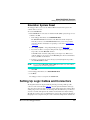
Manual Contents
The Microcontrollers Debugger Manual consists of the following books:
Book 1: Debugger engine - defines the HC08 and HC(S)08 common and base features,
their functionality, and a description of the components that are available in the debugger.
• Introduction
• Debugger Interface
• Debugger Components
• Control Points
• Real Time Kernel Awareness
• How To...
• CodeWarrior IDE Integration
• Debugger DDE Capabilities
• Synchronized Debugging Through DA-C IDE
Book 2: HC08 Debugger Connections - defines the connections available for debugging
code written for HC08 CPUs.
• Microcontroller Debugging First Steps
• HC08 Full Chip Simulation
• MON08 Interface Connection
• ICS MON08 Interface Connection
• HC08 P&E Multilink/Cyclone Pro Connection
• HC08 ICS P&E Multilink/Cyclone Pro Connections
• SofTec HC08 Connection
• HC08 FSICEBASE Emulator
Book 3: HCS08 Debugger Connections - defines the connections available for debugging
code written for HCS08 CPUs
• HCS08 Full Chip Simulation
• HCS08 P&E Multilink/Cyclone Pro Connection
• HCS08 Open Source BDM Connection
• HCS08 Serial Monitor Connection
• SofTec HCS08 Connection
Microcontrollers Debugger Manual
21
Manual Contents
• HCS08 On-Chip DBG Module
Book 4: RS08 Debug Connections
• RS08 Full Chip Simulation
• RS08 P&E Multilink/Cyclone Pro Connection
• RS08 Open Source BDM Connection
• SofTec RS08 Connection
Book 5: ColdFire V1.0 Debug Connections
• ColdFire V1 Full Chip Simulation Connection
• ColdFire P&E Multilink/Cyclone Pro Connection
• SofTec ColdFire Connection
• ColdFire On-Chip DBG Module
Book 6: Connection Common Features
• Flash Programming
• Debugging Memory Map
Book 7: Commands
• Debugger Engine Commands
Book 8: Environment Variables
• Debugger Engine Environment Variables
• Connection-Specific Environment Variables
Book 9: Debugger Legacy
• Legacy PEDebug Target Interface
• Legacy Target Interfaces Removed
• HC(S)08 Full-Chip Simulator Components No Longer Supported
NOTE
22
The Flexis series of devices is the 8- to 32-bit connection point on the Freescale
Controller Continuum, where complementary families of HCS08 and ColdFire
V1 microcontrollers share a common set of peripherals and development tools
to deliver migration flexibility.
These devices include the MC9S08QE128, MC9S08QE64, MC9S08QE96,
MCF51QE128, MCF51QE64, and MCF51QE96, which are covered in Book 3
and Book 5 respectively.
Microcontrollers Debugger Manual
Book I - Debugger Engine
Book I Contents
Each section of the Debugger manual includes information to help you become more
familiar with the Debugger, to use all its functions and help you understand how to use the
environment. This book, the Debugger engine, defines the HC(S)08, RS08, and
ColdFire® common and base features and their functionality, and gives a description of
the components that are available in the debugger.
This book is divided into the following chapters:
• This chapter describes the manual and special features of the Debugger.
• The Introduction Chapter introduces the Debugger concept.
• The Debugger Interface Chapter provides all details about the Debugger user
interface environment i.e., menus, toolbars, status bars and drag and drop facilities.
• The Debugger Components Chapter contains descriptions of each basic component
and visualization utility.
• The Control Points Chapter is dedicated to the control points and associated
windows.
• The Real Time Kernel Awareness Chapter contains descriptions of the Real Time
concept and related applications.
• The How To... Chapter provides answers for common questions and describes how
to use advanced features of the Debugger.
• The CodeWarrior IDE Integration chapter explains how to configure the Debugger
for use with the CodeWarrior IDE.
• The Debugger DDE Capabilities chapter describes the debugger DDE features.
• The Synchronized Debugging Through DA-C IDE chapter explains the use of tools
with the DA-C IDE from RistanCase
Microcontrollers Debugger Manual
23
Book I Contents
24
Microcontrollers Debugger Manual
1
Introduction
This section is an introduction to the Debugger from Freescale used in 8/16 bit embedded
applications.
Freescale Debugger
The Debugger is a member of the tool family for Embedded Development. It is a
Multipurpose Tool that you can use for various tasks in the embedded system and
industrial control world. Some typical tasks are:
• Simulation and debugging of an embedded application.
• Simulation and debugging of real-time embedded applications.
• Simulation and/or cross-debugging of an embedded application.
• Multi-Language Debugging: Assembly, C and C++
• True-Time Simulation
• User Components creation with the Peripheral Builder
• Simulation of a hardware design (e.g., board, processor, I/O chip).
• Building a target application using an object oriented approach.
• Building a host application controlling a plant using an object oriented approach.
Debugger Application
A Debugger Application contains the Debugger Engine and a set of debugger components
bound to the task that the components must perform (for example a simulation and
debugging session). The Debugger Engine is the heart of the system. It monitors and
coordinates the tasks of the components. Each Debugger Component has its own
functionality (e.g., source level debugging, profiling, I/O stimulation).
You can adapt your Debugger application to your specific needs. Integrating or removing
the Debugger Components is very easy. You can add additional Debugger Components
(for example, for simulation of a specific I/O peripheral chip) and integrate them with
your Debugger Application.
You can also open several components of the same type.
Microcontrollers Debugger Manual
25
Introduction
Debugger Features
Debugger Features
• True 32-bit application
• Powerful features for embedded debugging
• Special features for real time embedded debugging
• Powerful features for True Time Simulation
• Various and Same look Target Interfaces
• User Interface
• Versatile and intuitive drag and drop functions between components
• Folding and unfolding of objects like functions, structures, classes
• Graphical editing of user defined objects
• Visualization functions
• Smart interactions with objects
• Extensibility function
• Both Powerful Simulation & Debugger
• Show Me How Tool
• GUI (graphical user interface) version including command line
• Context sensitive help
• Configurable GUI with Tool Bar
• Smooth integration into third party tools
• Supports both Freescale and ELF/DWARF Object File Format and S-Records.
Demo Version Limitations on Components
When the Debugger is started in demo mode or with an invalid engine license, then all
components that are protected with FLEXlm are in demo mode. The limitations of all
components are described in their respective chapter.
26
Microcontrollers Debugger Manual
2
Debugger Interface
This chapter describes the Debugger Graphical User Interface (GUI). Topics include:
• Introduction
• Application Programs
• Starting the Debugger
• Debugger Main Window
• Component Associated Menus
• Highlights of the User Interface
Introduction
The CodeWarrior™ IDE main window acts as a container for windows of debugger
components. The main window provides a main menu bar, a tool bar, a status bar for
status information, and object information bars for several components.
The Debugger main window allows you to manage the layout of the different component
windows (Window menu of the Debugger application). Component windows are
organized as follows:
• Tiled arrangement - Auto tiled, component windows are automatically resized when
the main window is resized
• Component windows are overlapped
• Component windows that are currently minimized are Debugger Main window
icons.
Application Programs
The CodeWarrior IDE installer places executable programs in the prog subdirectory of
the CodeWarrior IDE installation directory. For example, installing the CodeWarrior IDE
software in C:\Program Files\Freescale, locates all program files in the folder
C:\Program Files\Freescale\CodeWarrior for Microcontrollers
V6.1\prog.
Microcontrollers Debugger Manual
27
Debugger Interface
Starting the Debugger
The following list is an overview of files that the CodeWarrior IDE uses for C/C++
debugging:
• hiwave.exe
Debugger executable file
• hibase.dll
Debugger main function dll
• elfload.dll
Debugger loader dll
• *.wnd
Debugger component
• *.tgt
Debugger target file
• *.cpu
Debugger CPU awareness file
Starting the Debugger
This section explains how you can start the debugger from within the CodeWarrior IDE or
from a DOS command line.
Starting from within the IDE
There are two ways to start the debugger from within the IDE, from a Project window
icon, or from the IDE Main Window menu bar.
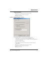
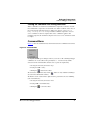
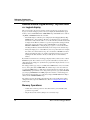
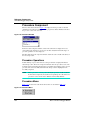
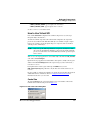
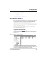
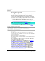
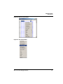
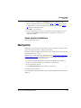
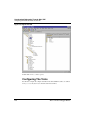
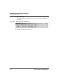
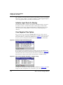
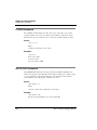
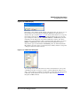
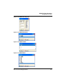
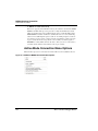
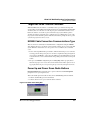
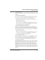
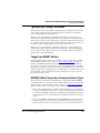
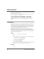
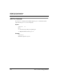
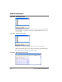
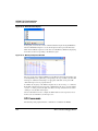
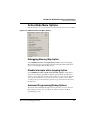
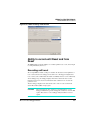
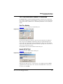
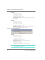
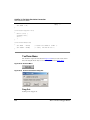
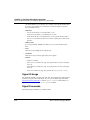
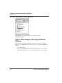
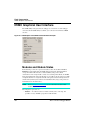
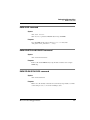
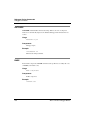
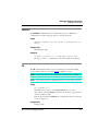
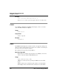
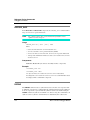
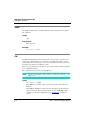
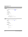
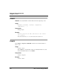
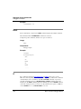
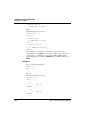
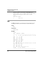
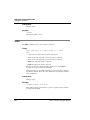
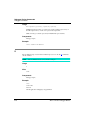
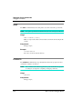
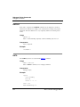
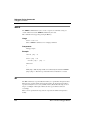
Starting Debug from the Project Window
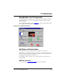
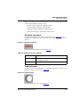
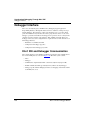
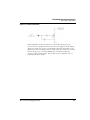
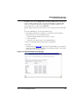
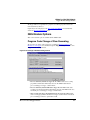
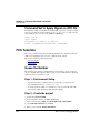
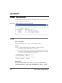
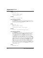
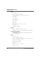
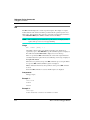
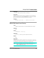
To start the debugger from the Project window, click the Debug icon (Figure 2.1), at the
top of the Project window.
Figure 2.1 Project Window Make and Debug Icons
28
Microcontrollers Debugger Manual
Debugger Interface
Starting the Debugger
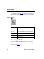
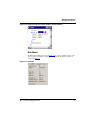
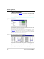
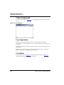
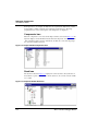
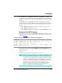
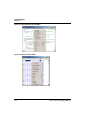
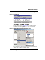
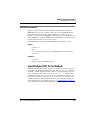
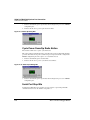
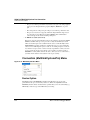
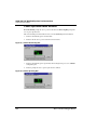
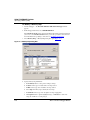
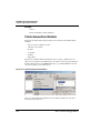
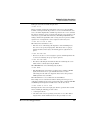
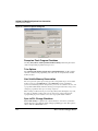
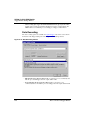
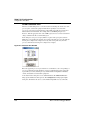
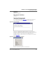
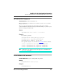
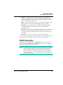
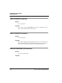
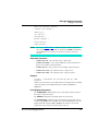
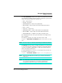
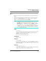
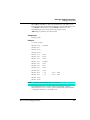
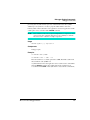
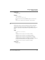
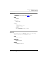
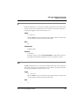
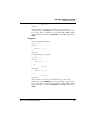
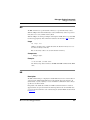
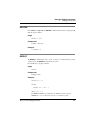
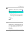
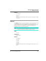
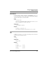
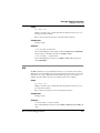
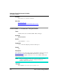
Starting Debug from the Main Window Menu Bar
You can also start the debugger from the main menu bar of the CodeWarrior IDE. To start
the debugger from the main menu bar, select Debug from the Project menu:
(Project > Debug.)
Figure 2.2 Main Window Project Menu
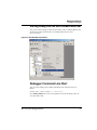
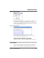
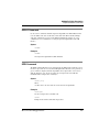
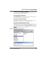
Debugger Command Line Start
You can start the debugger from a DOS command line. The command syntax is as
follows:
HIWAVE.EXE [<AbsFileName> {-<options>}]
where AbsFileName is the name of the application to load in the debugger. Precede
each option with a dash.
Microcontrollers Debugger Manual
29
Debugger Interface
Starting the Debugger
Command Line Options
DOS command line options are:
-T=<time>: Test mode
The debugger terminates after the specified time (in seconds). The default value is 300
seconds. For example:
c:\Program Files\Freescale\CodeWarrior for Microcontrollers
V6.1\prog\hiwave.exe -T=10
The above example instructs the debugger to terminate after 10 seconds.
-Target=<targetname>
This option sets the specified connection. For example:
C:\Program Files\Freescale\CodeWarrior for Microcontrollers
V6.1\prog\hiwave.exe c:\Program Files\Freescale\CodeWarrior
for Microcontrollers V6.1\demo\hc12\sim\fibo.abs -w Target=sim
The command in the above example starts the debugger and loads fibo.abs file.
-W: Wait mode
Debugger waits even when a <exeName> is specified.
-Instance=%currentTargetName
This option defines a build instance name. Once you define a build instance, the debugger
uses same build instance the next time you start the debugger. For example:
c:\Program Files\Freescale\CodeWarrior for Microcontrollers
V6.1\prog\hiwave.exe -Instance=%currentTargetName
If you attempt to start the debugger again, the existing instance of the debugger is brought
to the foreground.
-Prod= <fileName>
This option specifies the project directory and/or project file to be used at start-up. For
example:
c:\Program Files\Freescale\CodeWarrior for Microcontrollers
V6.1\prog\hiwave.exe -Prod=c:\demoproject\test.pjt
30
Microcontrollers Debugger Manual
Debugger Interface
Starting the Debugger
-Nodefaults
This prevents the debugger from loading the default layout. For example:
c:\Program Files\Freescale\CodeWarrior for Microcontrollers
V6.1\prog\hiwave.exe -nodefaults
-Cmd = <Command>
This option specifies a command to be executed at start-up: -cmd = {command}. For
example:
c:\Program Files\Freescale\CodeWarrior for Microcontrollers
V6.1\prog\hiwave.exe -cmd="open recorder"
-C <cmdFile>
This option specifies a command file to be executed at start-up. For example:
c:\Program Files\Freescale\CodeWarrior for Microcontrollers
V6.1\prog\hiwave.exe -c c:\temp\mycommandfile.txt
-ENVpath: "-Env" <Environment Variable> "=" <Variable
Setting>
This option sets an environment variable. This environment variable may be used to
overwrite system environment variables. For example:
c:\Program Files\Freescale\CodeWarrior for Microcontrollers
V6.1\prog\hiwave.exe -EnvOBJPATH=c:\sources\obj
NOTE
Options are not case sensitive.
Order of Commands
Commands specified by options are executed in the following order:
1. Load (activate) the project file (see below). If the project file is not specified,
project.ini is used by default.
2. Load <exeFile> if available and start running unless option |(W) was specified
3. Execute command file <cmdFile> if specified
4. Execute command if specified
5. Start running unless option |(W) was specified
NOTE
In version 6.1 of the debugger, the loaded program starts after all command and
command files are executed.
Microcontrollers Debugger Manual
31
Debugger Interface
Debugger Main Window
NOTE
The function Open in the File menu interprets any file without an .ini
extension as a command file and not a project file.
Example
C:\Program Files\Freescale\CodeWarrior for Microcontrollers
V6.1\PROG\DEMO\TEST.ABS -w -d
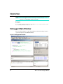
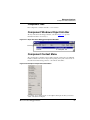
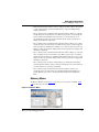
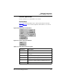
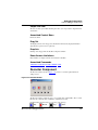
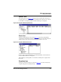
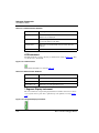
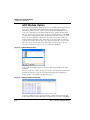
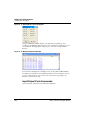
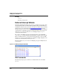
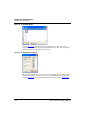
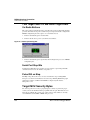
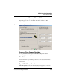
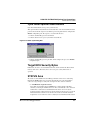
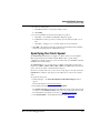
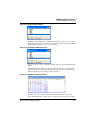
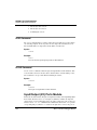
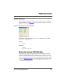
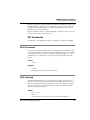
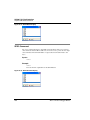
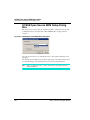
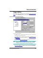
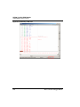
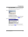
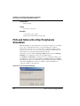
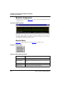
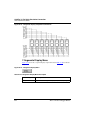
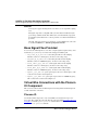
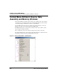
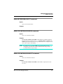
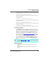
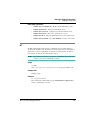
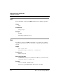
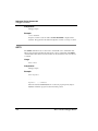
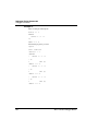
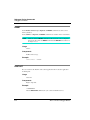
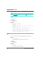
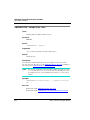
Debugger Main Window
Once you start the debugger, the True Time Simulator & Real Time Debugger window
opens in the right side of the IDE Main Window.
Figure 2.3 Debugger Main Window
32
Microcontrollers Debugger Manual
Debugger Interface
Debugger Main Window
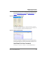
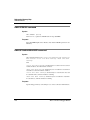
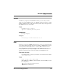
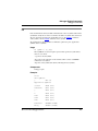
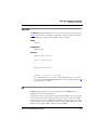
Debugger Main Window Toolbar
The Debugger Main Window toolbar is the default toolbar. Most of the Main Window
menu commands have a related shortcut icon on this toolbar. Figure 2.4 identifies each
default icon.
t
ar
ge
lt
Ha
st
ep
St
ep
ov
er
St
As
ep
se
ou
m
t
bl
y
st
ep
n
Ru
R
es
et
t
le
Si
ng
ic
lp
to
p
He
He
lp
on
y
st
e
Pa
op
C
Cu
t
n
e
Sa
v
pe
O
N
ew
Figure 2.4 Debugger Main Window Toolbar
A tool tip is available when you point the mouse at an icon.
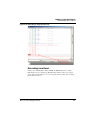
Debugger Main Window Status Bar
The status bar at the bottom of the Debugger Main Window, shown in Figure 2.5 contains
a context sensitive help line for connection specific information, e.g., number of CPU
cycles for the Simulator connection and execution status.
Figure 2.5 The Debugger Status Bar
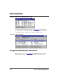
Main Window Menu Bar
The Debugger Main Window Menu Bar, shown in Figure 2.6 is associated with the main
function of the debugger application, connection, and selected windows.
Figure 2.6 Debugger Window Menu Bar
NOTE
You can select menu commands by pressing the ALT key to select the menu
bar then press the key corresponding to the underlined letter in the menu
command.
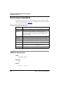
Table 2.1 describes menu entries available in the menu bar.
Microcontrollers Debugger Manual
33
Debugger Interface
Debugger Main Window
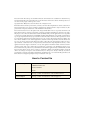
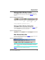
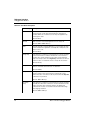
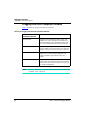
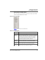
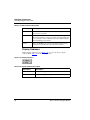
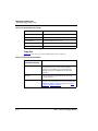
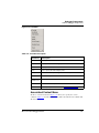
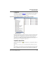
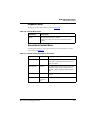
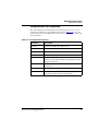
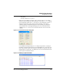
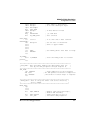
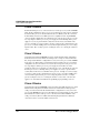
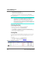
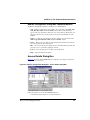
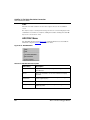
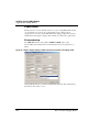
Table 2.1 Description of the Main Menu Toolbar Entries
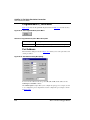
Menu entry
Description
File
Contains entries to manage debugger configuration files.
View
Contains entries to configure the toolbar.
Run
Contains entries to monitor a simulation or debug session.
Connection
Contains entries to select the debugger connection. Once a
connection has been selected, the name of this heading
changes.
Component
Contains entries to select and configure extra component
window.
Data
Contains entries to select Data component functions.
Window
Contains entries to set the component windows.
Help
A standard Windows Help menu.
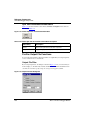
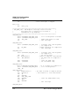
File Menu
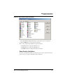
The File menu shown in Figure 2.7 is dedicated to the debugger project.
Figure 2.7 File Menu
34
Microcontrollers Debugger Manual
Debugger Interface
Debugger Main Window
Table 2.2 describes File Menu entries.
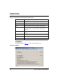
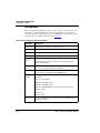
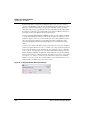
Table 2.2 File Menu Entry Description
Menu Entry
Description
New
Creates a new project.
Load Application
Loads an executable file (or debugger connection if nothing is
selected).
...\restart.abs
Recent applications list
...\await.abs
...
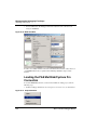
Open Configuration
Opens the debugger project window. You can load a project file
.PJT or .INI. Additionally you can load an existing .HWC file
corresponding to a debugger configuration file. You can load a
project .INI file containing component names, associated
window positions and parameters, window parameters (fonts,
background colors, etc.), connection name (e.g., Simulator)
and the .ABS application file to load.
Save Configuration
Saves the project file.
Save Project As
Opens the debugger project window to save the project file
under a different path and name, and format (PJT; INI...).
Configuration
Opens the Preferences window to set environment variables for
current project.
1.Project.ini
Recent project file list.
2.Test.ini
3...
Exit
Quits the Debugger.
You can shortcut some of these functions by clicking toolbar icons (refer to the Debugger
Main Window Toolbar section).
Microcontrollers Debugger Manual
35
Debugger Interface
Debugger Main Window
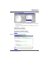
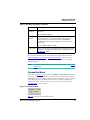
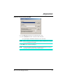
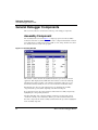
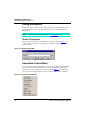
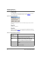
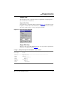
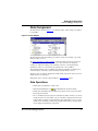
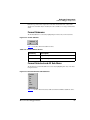
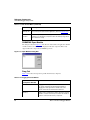
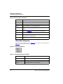
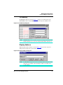
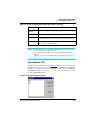
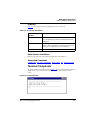
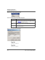
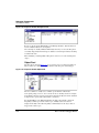
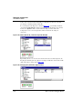
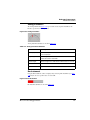
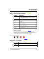
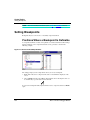
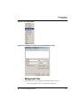
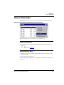
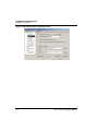
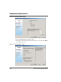
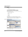
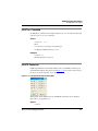
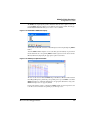
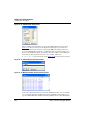
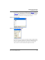
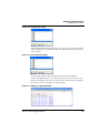
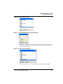
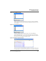
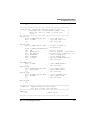
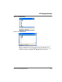
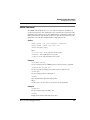
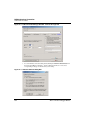
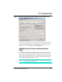
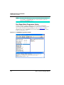
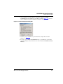
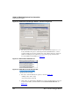
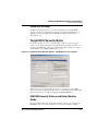
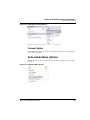
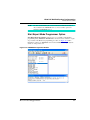
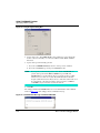
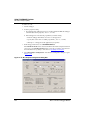
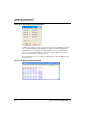
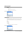
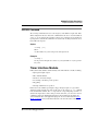
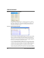
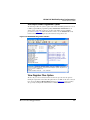
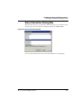
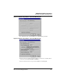
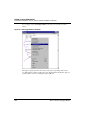
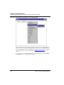
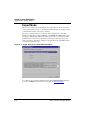
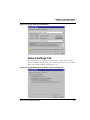
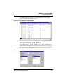
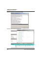
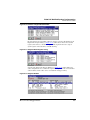
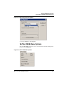
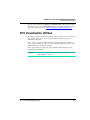
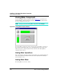
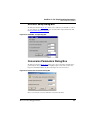
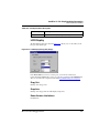
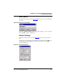
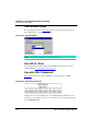
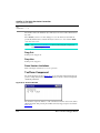
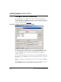
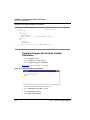
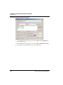
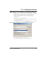
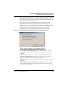
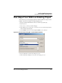
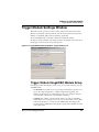
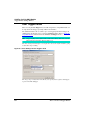
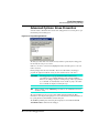
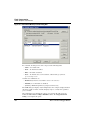
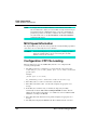
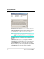
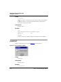
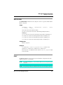
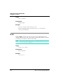
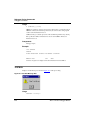
Configuration Window
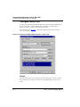
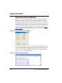
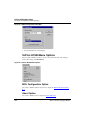
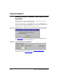
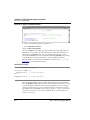
Open the Configuration window by selecting Configuration from the Files menu. With
this window (Figure 2.8) it is possible to set up environment variables for the current
project. New variables are saved in the current project file when you click the OK button.
NOTE
The corresponding menu entry (File > Configuration) is only enabled if a
project file is loaded.
Figure 2.8 Configuration Window - Environment Tab
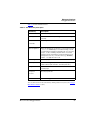
The Configuration Window - Environment tab contains the following controls:
• A list box containing all available environment variables. You can select a variable
with the mouse or Up/Down buttons.
• Command Line Arguments are displayed in the text box. You can add, delete, or
modify options, and specify a directory with the browse button (...).
• A second list box contains the arguments for all of the environment variables defined
in the corresponding Environment section. Select a variable with the mouse or Up/
Down buttons.
36
Microcontrollers Debugger Manual
Debugger Interface
Debugger Main Window
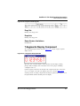
Command Buttons:
• OK: Changes are confirmed and saved in current project file.
• Cancel: Closes dialog box without saving changes.
• Help: Opens the help file.
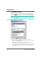
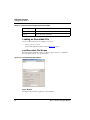
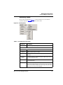
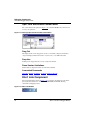
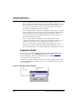
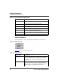
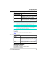
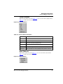
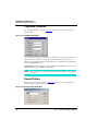
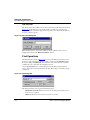
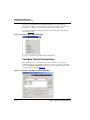
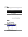
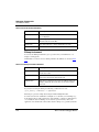
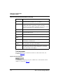
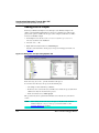
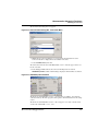
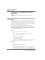
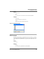
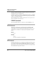
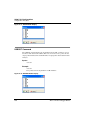
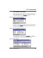
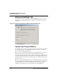
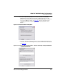
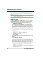
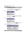
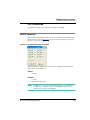
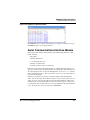
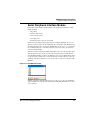
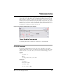
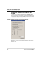
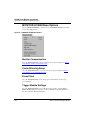
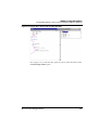
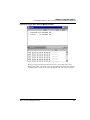
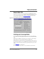
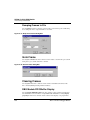
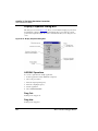
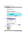
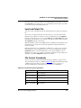
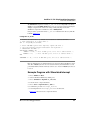
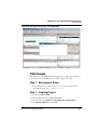
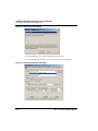
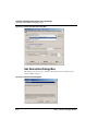
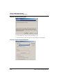
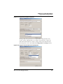
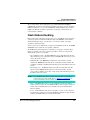
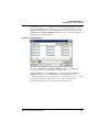
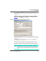
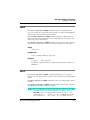
Figure 2.9 Configuration Window - Load Tab
The Configuration Window - Load tab contains the following controls:
• Automatically erase and program into FLASH and EEPROM checkbox.
• A Verify memory image after loading code checkbox, with two radio buttons that let
you define the memory image.
• Run after successful load checkbox.
• A Stop at Function checkbox with a textbox that lets you define the function.
Command Buttons:
OK: Changes are confirmed and saved in current project file.
Cancel: Closes dialog box without saving changes.
Help: Opens the help file.
Microcontrollers Debugger Manual
37
Debugger Interface
Debugger Main Window
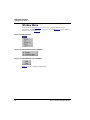
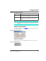
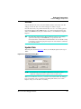
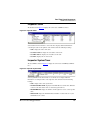
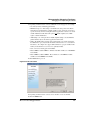
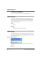
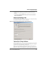
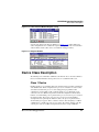
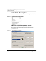
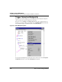
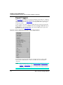
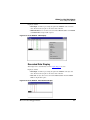
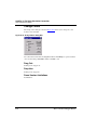
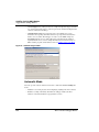
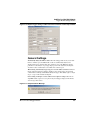
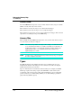
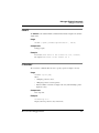
View Menu
In the Main Window View menu (Figure 2.10) you can choose to show or hide the toolbar,
status bar, window component titles and headlines (see the Component Windows Object
Info Bar). You can select smaller window borders and customize the toolbar. Table 2.3
describes the View Menu entries.
Figure 2.10 View Menu
Table 2.3 View Menu Description
Menu Entry
Description
Toolbar
Check / uncheck Toolbar if you want to display or hide it.
Status Bar
Check / uncheck Status Bar if you want to display or hide it.
Hide Tile
Check / uncheck Hide Title if you want to hide or display the
window title.
Hide Headline
Check / uncheck Hide Headline if you want to hide or display the
headline.
Small Borders
Check / uncheck Small Border if you want to display or hide
small window borders.
Customize
Opens the debugger Customize Toolbar window.
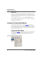
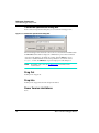
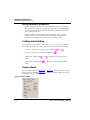
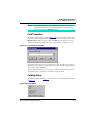
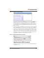
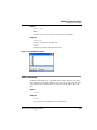
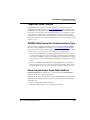
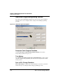
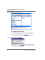
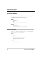
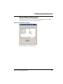
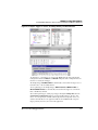
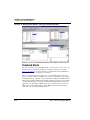
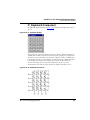
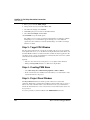
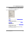
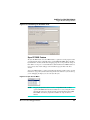
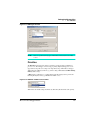
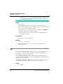
Customizing the Toolbar
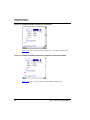
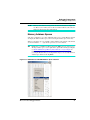
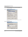
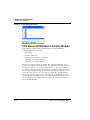
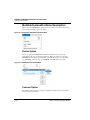
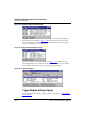
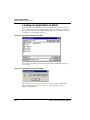
When you select Customize from the View menu, the Customize Toolbar dialog box
appears. You can customize the toolbar of the Debugger, adding and removing component
shortcuts and action shortcuts in this dialog box. You can also insert separators to separate
icons. Almost all functions in View, Run and Window menus are available as shortcut
buttons, as shown in Figure 2.11.
38
Microcontrollers Debugger Manual
Debugger Interface
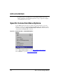
Debugger Main Window
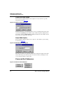
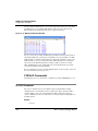
Figure 2.11 Customize Toolbar Dialog Box
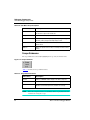
• Select the desired shortcut button in the Available buttons list box and click Add to
install it in the toolbar.
• Select a button in the Toolbar buttons list box and click Remove to remove it from
the toolbar.
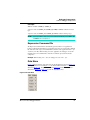
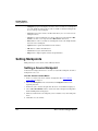
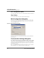
Demo Version Limitations
The default toolbar cannot be configured.
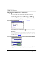
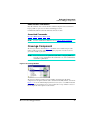
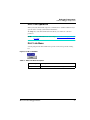
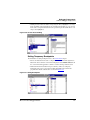
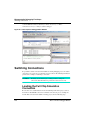
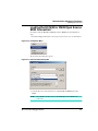
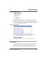
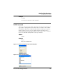
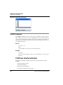
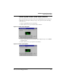
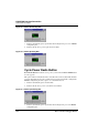
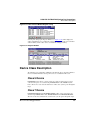
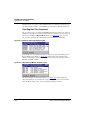
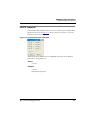
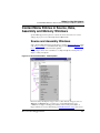
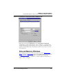
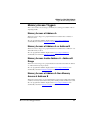
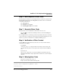
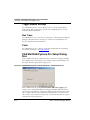
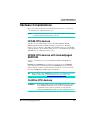
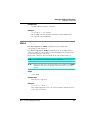
Examples of View Menu Options
Figure 2.12 shows a typical component window display.
Figure 2.12 Typical Component Window Display
Figure 2.13 shows a component window without a title and headline.
Microcontrollers Debugger Manual
39
Debugger Interface
Debugger Main Window
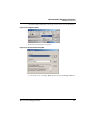
Figure 2.13 Component Window without Title and Headline
Figure 2.14 shows a component window without a title and headline, and with a small
border.
Figure 2.14 Component Window without Title and Headline, and with Small Border
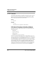
Figure 2.15 shows a component window without headline and small border
40
Microcontrollers Debugger Manual
Debugger Interface
Debugger Main Window
Figure 2.15 Component Window without Headline and Small Border
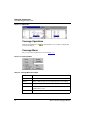
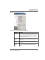
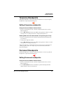
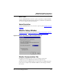
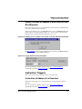
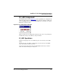
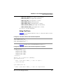
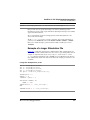
Run Menu
The Main Window Run menu, shown in Figure 2.16 is associated with the debug session.
You can monitor a simulation or debug session from this menu. Run menu entries are
described in Table 2.4.
Figure 2.16 Run Menu
Microcontrollers Debugger Manual
41
Debugger Interface
Debugger Main Window
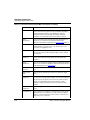
Table 2.4 Run Menu Description
Menu entry
Description
Start/Continue
Starts or continues execution of the loaded application from the
current program counter (PC) until a breakpoint or watchpoint is
reached, runtime error is detected, or user stops the application by
selecting Run > Halt.
Shortcut: F5 key
Restart
Starts execution of the loaded application from its entry point.
Shortcut: CTRL + Shift + F5 keys
Halt
Interrupts and halts a running application. You can examine the state
of each variable in the application, set breakpoints, watchpoints, and
inspect source code.
Shortcut: F6 key
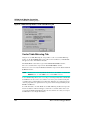
Single Step
If the application is halted, this command performs a single step at the
source level. Execution continues until the next source reference is
reached. If the current statement is a procedure call, the debugger
“steps into” that procedure. The Single Step command does not treat
a function call as one statement, therefore it steps into the function.
Shortcut: F11 key
Step Over
Similar to the Single Step command, but does not step into called
functions. A function call is treated as one statement.
Shortcut: F10 key
Step Out
If the application is halted inside of a function, this command continues
execution and then stops at the instruction following the current
function invocation. If no function calls are present, then the Step Out
command is not performed.
Shortcut: Shift + F11 keys
Assembly
Step
If the application is halted, this command performs a single step at the
assembly level. Execution continues for one CPU instruction from the
point it was halted. This command is similar to the Single Step
command, but executes one machine instruction rather than a high
level language statement.
Shortcut: CTRL + F11 keys
42
Microcontrollers Debugger Manual
Debugger Interface
Debugger Main Window
Table 2.4 Run Menu Description (continued)
Menu entry
Description
Assembly
Step Over
Similar to the Step Over command, but steps over subroutine call
instructions.
Shortcut: CRTL + F10 keys
Assembly
Step Out
If the application is halted inside a function, this command continues
execution and stops on the CPU instruction following the current
function invocation. This command is similar to the Step Out
command, but stops before the assignment of the result from the
function call.
Shortcut: CTRL + Shift + F11 keys
Control Points
Opens the Controlpoints Configuration Window that contains tabs that
allow you to control Breakpoints, Watchpoints and Markpoints (refer to
Control Points chapter).
You can provide shortcuts for some of these functions using the toolbar. Refer to the
Debugger Main Window Toolbar and Customizing the Toolbar sections for details.
You can also set breakpoints and watchpoints from within the Source and Assembly
component windows.
NOTE
For more information about breakpoints and watchpoints, refer to the Control
Points chapter.
Connection Menu
This menu entry (Figure 2.17) appears between the Run and Component menus when no
connection is specified in the PROJECT.INI file and no connection has been set. The
Connection name is replaced by an actual connection name when the connection is set. If
a connection has been set, the number of menu entries is expanded, depending on the
connection. To set the connection, select Component > Set Connection. Refer to the
Component Menu section for details.
Figure 2.17 Connection Menu
Table 2.5 describes the Connection Menu entries.
Microcontrollers Debugger Manual
43
Debugger Interface
Debugger Main Window
Table 2.5 Connection Menu Common Option Description
Menu Entry
Description
Load
Loads a connection.
Reset
Resets the current connection.
Loading an Executable File
Use the Connection menu to load a debugger connection:
• Choose Connection > Load
The Load Executable File window shown in Figure 2.18 appears.
Load Executable File Window
From the Load Executable File window, set the load options and choose a Simulation
Execution Framework (an .ABS application file).
Figure 2.18 Load Executable File Window
Open Button
Pressing this button loads the application code and symbols.
44
Microcontrollers Debugger Manual
Debugger Interface
Debugger Main Window
Load Options Buttons
These three buttons allow you to select which part of the executable file to load:
• Load Code Button: Loads the application code only. Loads only the application into
the target system. Use this button if no debugging is needed.
• Load Symbols Button: Loads symbols only. Loads only debugging information.
This button can be used if the code is already loaded into the target system or
programmed into a non-volatile memory device (ROM/FLASH).
• Verify Code Button: Loader loads no data into memory. However, it reads back
current data matching the same areas from the target memory and compares all data
with the data from the selected file.
Open and Load Code Options Area
The checkboxes and buttons of this area of the Load Executable File window offer the
following options:
• A checkbox to Automatically erase and program into FLASH and EEPROM.
• A Verify memory image after loading code checkbox, with two radio buttons that let
you define the memory image.
• Run after successful load checkbox.
• A Stop at Function checkbox with a textbox that lets you define the function.
Command Buttons:
OK: Changes are confirmed and saved in current project file.
Cancel: Closes dialog box without saving changes.
Help: Opens the help file.
Connection Command File Window
From the Connection menu, choose Command File to open the Connection Command
File window. Each tab of this window, shown in Figure 2.19 corresponds to an event on
which a command file can be automatically run.
See the Startup Command File, Reset Command File, Preload Command File, and
Postload Command File, sections that follow. Although these command files are not
generated automatically, you can install them when installing a new connection. However,
the Debugger recognizes these command files and executes them. Depending on the
connection used, other command files can be recognized by the Debugger. Refer to the
appropriate connection chapter for command file information and properties.
Microcontrollers Debugger Manual
45
Debugger Interface
Debugger Main Window
Figure 2.19 Connection Command File Window
The command file in the edit box is executed when the corresponding event occurs. Click
the Browse button to set the path and name of the command file.
The Enable Command File check box allows you to enable/disable a command file on an
event. By default, all command files are enabled:
• The default Startup command file is STARTUP.CMD
• The default Reset command file is RESET.CMD
• The default Preload command file is PRELOAD.CMD
• The default Postload command file is POSTLOAD.CMD
NOTE
Startup settings performed in this dialog box are stored for subsequent
debugging sessions in the [Simulator] section of the PROJECT file using the
variable CMDFILE0.
NOTE
When a CPU is set, the settings performed in this dialog box are stored for
subsequent debugging sessions in the [Simulator XXX] (where XXX is the
processor) section of the PROJECT file using variables CMDFILE0,
CMDFILE1 ... CMDFILEn.
Startup Command File
The startup.cmd command file is a Debugger system command file. The Startup
command file executes after you load the connection (the target defined in the project.ini
file or when you select Component > Set Connection).
You can specify the Startup command file full name and status (enable/disable) either
with the CMDFILE STARTUP Command Line command or using the Startup property
tab of the Connection Command File Window.
46
Microcontrollers Debugger Manual
Debugger Interface
Debugger Main Window
The default settings enable the STARTUP.CMD file located in the current project directory
as the current Startup command file.
Reset Command File
The reset.cmd command file is a Debugger system command file. The Reset
command file executes after clicking the reset button, selecting Connection Name > Reset
in the menu (Connection Name is the real name of the connection, such as MMDS0508
or SDI) reset.cmd or selecting Command Line command.
Specify the Reset command file full name and status (enable/disable) either with the
CMDFILE RESET Command Line command or using the Reset property tab of the
Connection Command File Window.
The default settings enable the RESET.CMD file located in the current project directory as
the current Reset command file.
Preload Command File
The preload.cmd command file is a Debugger system command file. The Preload
command file executes before an application loads to the target system through the
connection, or by selecting Connection Name > Load.
Specify the Preload command file full name and status (enable/disable) either with the
CMDFILE PRELOAD Command Line command or using the Preload property tab of the
Connection Command File Window.
The default settings enable the PRELOAD.CMD file located in the current project directory
as the current Preload command file.
Postload Command File
The postload.cmd command file is a Debugger system command file. Postload
executes after an application loads to the target system through the connection, or by
selecting Connection Name > Load.
Specify the Postload command file full name and status (enable/disable) either with the
CMDFILE POSTLOAD Command Line command or by using the Postload property tab
of the Connection Command File Window.
The default settings enable the POSTLOAD.CMD file located in the current project
director as the current Postload command file.
Component Menu
The Component menu is shown in Figure 2.20.
Microcontrollers Debugger Manual
47
Debugger Interface
Debugger Main Window
Figure 2.20 Component Menu
Table 2.6 describes the Component Menu entries.
Table 2.6 Component Menu Description
Menu entry
Description
Open
Loads an extra component window that has not been loaded by
the Debugger at startup. The context-sensitive dialog box
presents a set of different components that are introduced in the
Typical Component Window Display section.
Set Connection
Sets the Debugger connection.
Fonts
Opens a standard Font Selection dialog box, where you can set
the font used by Debugger components.
Background Color
Opens a standard Color Selection dialog box, where you can
set the background color used by the Debugger component
windows.
NOTE
For a readable display, we recommend using a proportional font (e.g., Courier,
Terminal, etc.).
Select Component > Open to load an extra component window that has not been loaded by
the Debugger at startup. The context-sensitive dialog box presents a set of different
components that are introduced in Debugger Components.
Select Component > Set Connection and the Set Connection dialog box shown in Figure
2.21 is opened.
48
Microcontrollers Debugger Manual
Debugger Interface
Debugger Main Window
Figure 2.21 Set Connection Dialog Box
6. Use the Processor list menu to select the desired processor.
7. Use the connection list menu to select the desired connection.
A text panel displays information about the selected connection.
NOTE
When a connection cannot be loaded, the combo box displays the correct path
for you to install the missing DLL.
8. Click OK to load connection in debugger.
NOTE
For more information about which connection to load and how to set/reset a
connection, refer to the other sections of this manual.
Microcontrollers Debugger Manual
49
Debugger Interface
Debugger Main Window
Window Menu
In this menu, shown in Figure 2.22, you can set the component windows general
arrangement. The Submenu Window > Options is shown in Figure 2.23 and the Submenu
Window > Layout in Figure 2.24.
Figure 2.22 Window Menu
Figure 2.23 Window Menu Options SubMenu
Figure 2.24 Window Menu Layout SubMenu
Table 2.7 specifies the Window Menu entries.
50
Microcontrollers Debugger Manual
Debugger Interface
Debugger Main Window
Table 2.7 Window Menu Description
Menu entry
Description
Cascade
Option to arrange all open windows in cascade (so they
overlap).
Tile
Option to display all open windows in tile format (non
overlapping).
Arrange Icons
Arranges icons at the bottom of windows.
Options - Autosize
Component windows always fit into the debugger window
whenever you modify the debugger window size.
Options Component Menu
When a component window is selected, the associated menu is
displayed in the main menu. For example if you select the
Source window, the Source menu is displayed in the main
menu.
Layout - Load/Store
Option to Load / Store your arrangements from a .HWL file.
NOTE
Autosize and Component Menu are checked by default.
Help Menu
This is the Debugger Main window Help menu (Figure 2.25). Table 2.8 shows menu
entries.
Figure 2.25 Help Menu
Table 2.8 Help Menu Description
Menu entry
Description
Help Topics
Choose Help Topics in the menu for online help or if you need
specific information about a topic.
About
Information about the debugger version and copyright, and
license information is displayed.
Microcontrollers Debugger Manual
51
Debugger Interface
Component Associated Menus
About Box
Select Help > About to display the About box. The about box lists directories for the
current project, system information, program information, version number and copyright.
It contains information to send for Registration. You can copy this information and send to
[email protected].
For more information on all components, click on the Extended Information button.
Two hypertext links allow you to send an E-mail for a license request or information, and
open the Freescale internet home page.
Click on OK to close this dialog box.
Component Associated Menus
Various Debugger Component windows are shown in Figure 2.3. Each component
window loaded by default or that you have loaded has two menus. One menu is in the
main menu and the other one is a context menu (also called Associated Context Menu) that
you can open by right-clicking in a window component. Note that before right-clicking,
the component window has to be active.
Component Main Menu
This menu, shown in Figure 2.26 is always between the Component entry and the Window
entry of the Debugger main window toolbar. It contains general entries of the current
active component. You can hide this menu by unchecking Window > Options >
Component Menu.
Figure 2.26 Example of Component Main Menu
52
Microcontrollers Debugger Manual
Debugger Interface
Component Associated Menus
Component Files
Each component is a windows file with a .wnd extension
Component Windows Object Info Bar
The object info bar of the debugger window, as shown in Figure 2.27, provides
information about the selected object.
Figure 2.27 Object Info Bar of Debugger Component Windows
Component Context Menu
The context menu is a dynamic context sensitive menu. It contains entries for additional
facilities available in the current component. Depending on the position of the mouse in
the window and what is being pointed to, context menu entries differ.
Figure 2.28 Example of Component Context Menu
For example, if you click the mouse on a breakpoint, menu options allow you to delete,
enable, or disable the breakpoint.
Microcontrollers Debugger Manual
53
Debugger Interface
Highlights of the User Interface
Highlights of the User Interface
This section describes some of the main features of the Debugger user interface.
Activating Services with Drag and Drop
You can activate services by dragging objects from one component window to another.
This is known as drag and drop, an example is shown in Figure 2.29.
Figure 2.29 Drag and Drop Example
When the dragged item is not allowed in the destination to which you are dragging the
item, the following cursor symbol is displayed:
Example:
You can activate the display of coverage information on assembler and C statements by
dragging the chosen procedure name from the Coverage component to the Source and
Assembly components (Figure 2.30).
Figure 2.30 Dragging Procedure Name from Coverage to Source Component Window
You can display the memory layout corresponding to the address held in a register by
dragging the address from the Register Component to the Memory Component.
54
Microcontrollers Debugger Manual
Debugger Interface
Highlights of the User Interface
To Drag and Drop an Object
To drag an object from one component window to another:
1. Select the component containing the object you want to drag.
2. Make sure the destination component window where you want to drag the object is
visible.
3. Select the object you want.
4. Press and hold the left mouse button, drag the object into the destination component
window and then release the mouse button.
Drag and Drop Combinations
Dragging and dropping objects is possible between different component windows and are
introduced in each component description section.
See below, the possible combinations of drag and drop between components and
associated actions. When additional components are available, new combinations might
be possible and described in the component’s information manual.
Dragging from Assembly Component Window
Table 2.9 summarizes dragging from the Assembly Component.
Table 2.9 Dragging from the Assembly Component Window
Destination
Component Window
Action
Command Line
The Command Line component appends the address of
the “pointed to” instruction to the current command.
Memory
Dumps memory starting at the selected instruction PC.
The PC location is selected in the memory component.
Register
Loads the destination register with the PC of the selected
instruction.
Source
Source component scrolls up to the source statements
and highlights it.
Microcontrollers Debugger Manual
55
Debugger Interface
Highlights of the User Interface
Dragging from Data Component Window
Table 2.10 summarizes dragging from the Data Component.
Table 2.10 Dragging from the Data Component Window
Destination
Component Window
Action
Command Line
Dragging the name appends the address range of the
variable to the current command in the Command Line
Window. Dragging the value appends the variable value
to the current command in the Command Line Window.
Memory
Dumps memory starting at the address where the
selected variable is located. The memory area where the
variable is located is selected in the memory component.
Register
Dragging the name loads the destination register with the
address of the selected variable. Dragging the value
loads the destination register with the value of the
variable.
Source
Dragging the name of a global variable in the source
window displays the module where the variable is defined
and the source text is searched for the first occurrence of
the variable and highlighted.
NOTE
56
It is not possible to drag an expression defined with the Expression Editor. The
“forbidden” cursor is displayed.
Microcontrollers Debugger Manual
Debugger Interface
Highlights of the User Interface
Dragging from Source Component Window
Table 2.11 summarizes dragging from the Source Component.
Table 2.11 Dragging from the Source Component Window
Destination Component
Window
Action
Assembly
Displays disassembled instructions starting at the first
high level language instruction selected. The assembler
instructions corresponding to the selected high level
language instructions are highlighted in the Assembly
component
Register
Loads the destination register with the PC of the first
instruction selected.
Memory
Displays the memory area corresponding with the high
level language source code selected. The memory area
corresponding to the selected instructions are grayed in
the memory component.
Data
A selection in the Source window is considered an
expression in the Data window, as if it was entered
through the Expression Editor of the Data component.
(See Data Component and Expression Editor.)
Microcontrollers Debugger Manual
57
Debugger Interface
Highlights of the User Interface
Dragging from the Memory Component Window
Table 2.12 summarizes dragging from the Memory Component.
Table 2.12 Dragging from the Memory Component Window
Destination
Component Window
Action
Assembly
Displays disassembled instructions starting at the first
address selected. Instructions corresponding to the
selected memory area are highlighted in the Assembly
component.
Command Line
Appends the selected memory range to the Command
Line window.
Register
Loads the destination register with the start address of the
selected memory block.
Source
Displays high level language source code starting at the
first address selected. Instructions corresponding to the
selected memory area are grayed in the source
component.
Dragging from Procedure Component Window
Table 2.13 summarizes dragging from the Procedure Component.
Table 2.13 Dragging from the Procedure Component Window
Destination
Component Window
Action
Data > Local
Displays local variables from the selected procedure in
the data component.
Source
Displays source code of the selected procedure. Current
instruction inside the procedure is highlighted in the
Source component.
Assembly
The current assembly statement inside the procedure is
highlighted in the Assembly component.
Dragging from Register Component Window
Table 2.14 summarizes dragging from the Register Component Window.
58
Microcontrollers Debugger Manual
Debugger Interface
Highlights of the User Interface
Table 2.14 Dragging from the Register Component Window
Destination
Component Window
Action
Assembly
Assembly component receives an address range, scrolls
to the corresponding instruction and highlights it.
Memory
Dumps memory starting at the address stored in the
selected register. The corresponding address is selected
in the memory component.
Dragging from Module Component Window
Table 2.15 summarizes dragging from the Register Component.
Table 2.15 Dragging from the Module Component Window
Destination
Component Window
Action
Data > Global
Displays global variables from the selected module in the
data component.
Memory
Dumps memory starting at the address of the first global
variable in the module. The memory area where this
variable is located is selected in the memory component.
Source
Displays source code from selected module.
Selection Dialog Box
This dialog box is used in the Debugger for opening general components or source files.
You can select the desired item with the arrow keys or mouse and then the OK button to
accept or CANCEL to ignore your choice. The HELP button opens this section in the
Help File.
This dialog box is used for the following selections:
• Set Connection
• Open IO component
• Open Source File
• Open Module
• Individual component window
Microcontrollers Debugger Manual
59
Debugger Interface
Highlights of the User Interface
60
Microcontrollers Debugger Manual
3
Debugger Components
This chapter explains how the different components of the Debugger work. This chapter
contains the following sections:
• Component Introduction
• Loading Component Windows
• General Debugger Components
• Visualization Utilities
Component Introduction
The Debugger kernel includes various components.
CPU Components
CPU components handle processor-specific properties such as register naming, instruction
decoding (disassembling), and stack tracing. A specific implementation of the CPU
module must be provided for each processor type that is supported in the debugger. The
CPU-related component is not introduced in this section. However, the Register
component, Memory component, and all other Connection-dependent components reflect
this system component. The appropriate CPU component loads automatically when
loading an application or executable file (.ABS file), therefore it is possible to mix
applications for different MCUs. The Debugger automatically detects the MCU type and
loads the appropriate CPU component, if available on your environment.
Window Components
The Debugger main window components are small applications loaded into the debugger
framework at run-time. Window components can access all global facilities of the
debugger engine, such as the connection (to communicate with different connections), and
the symbol table. The Debugger window components are implemented as dynamic link
libraries (DLLs) with extension .WND. These components are introduced in this section.
Microcontrollers Debugger Manual
61
Debugger Components
Component Introduction
Connection Components
Different debugger connections are available. For example, you can set a CPU awareness
to simulate your .ABS application files, and also set a background debugger.
Different connections are available to connect the target system (hardware) to the
debugger. For example, the connection may be connected using a Full Chip Simulator, an
Emulator, a ROM monitor, a BDM pod cable, or any other supported device.
NOTE
Connection components are introduced in their respective manuals.
Loading Component Windows
In the Debugger Main Window Menu Bar, shown in Figure 3.1, you can use the
Component menu to load all framework components. Each Debugger component you
select appears as a window in the Debugger main window.
Figure 3.1 Debugger Window Menu Bar
To open the window that lets you choose one or more components:
1. Choose Component > Open
2. In the Open Window Component window shown in Figure 3.2, select the desired
component.
NOTE
62
To open more than one component, select multiple components.
Microcontrollers Debugger Manual
Debugger Components
Component Introduction
Figure 3.2 Open Window Component Window
3. In the Open Window Component window, use the mouse to select a component.
4. Click the OK button to open the selected component.
There are three tabs in the Open Window Component window:
• The Icon tab shows components with large icons.
• The List tab shows components with small icons.
• The Details tab shows components with their description.
Demo Version Limitations
The demo version limits the number of components you can open at a time. If you use the
demo version, you can open a maximum of eight components.
Microcontrollers Debugger Manual
63
Debugger Components
General Debugger Components
General Debugger Components
This section describes the various features and usage of the debugger components.
Assembly Component
The Assembly window, shown in Figure 3.3, displays program code in disassembled
form. It has a function very similar to that of the Source component window but on a much
lower abstraction level. Thus it is therefore possible to view, change, monitor and control
the current location of execution in a program.
Figure 3.3 Assembly Window
This window contains all on-line disassembled instructions generated by the loaded
application. Each displayed disassembled line in the window can show the following
information: the address, machine code, instruction and absolute address in case of a
branch instruction. By default, the user can see the instruction and absolute address.
If breakpoints have been set in the application, they are marked in the Assembly
component with a special symbol, depending on the kind of breakpoint.
If execution has stopped, the current position is marked in the Assembly component by
highlighting the corresponding instruction.
The Object Info Bar of the component window contains the procedure name, which
contains the currently selected instruction. When a procedure is double clicked in the
Procedure component, the current assembly statement inside this procedure is highlighted
in the Assembly component.
64
Microcontrollers Debugger Manual
Debugger Components
General Debugger Components
Assembly Menu
The Assembly menu shown in Figure 3.4 contains all functions associated with the
assembly component. Table 3.1 describes these menu entries.
Figure 3.4 Assembly Menu
Table 3.1 Assembly Menu Description
Menu Entry
Description
Address
Opens a dialog box prompting for an address: Show PC.
Display
Code
Displays machine code in front of each disassembled instruction.
Symbolic
Displays symbolic names of objects.
Address
Displays the location address at the beginning of each disassembled
instruction.
Absolute
Address
In a branch instruction, displays the absolute address at the end of
the disassembled instruction.
Format
Select formatting; choose Auto, Hexadecimal, Octal, Binary, Decimal,
or Unsigned Decimal
Freeze
Both the Assembly and Source components can be frozon. These
components usually display the code execution from the current PC.
When you freeze these components, they no longer follow the current
PC but are frozen to their current displays.
Microcontrollers Debugger Manual
65
Debugger Components
General Debugger Components
Setting Breakpoints
Breakpoints can be set, edited and deleted when using the context menu. Right-click on
any statement in the Source component window, then choose Set Breakpoint, Delete
Breakpoint, etc.
NOTE
For information on using breakpoints, see Control Points chapter.
Show PC Dialog Box
If a hexadecimal address is entered in the Show PC dialog box shown in Figure 3.5,
memory contents are interpreted and displayed as assembler instructions starting at the
specified address.
Figure 3.5 Show PC Dialog Box
Associated Context Menu
To open the context menu right-click in the text area of the Assembly component window.
The context menu contains default menu entries for the Assembly component. It also
contains some context dependent menu entries described in Table 3.2; depending on the
current state of the debugger. Menu contents vary when the DBG module is available.
Figure 3.6 Assembly Context Menu
66
Microcontrollers Debugger Manual
Debugger Components
General Debugger Components
Table 3.2 Assembly Context Menu Description
Menu Entry
Description
Set Breakpoint
Appears only in the context menu if no breakpoint is set or
disabled on the pointed to instruction. When selected, sets a
permanent breakpoint on this instruction. When program
execution reaches this instruction, the program is halted and the
current program state is displayed in all window components.
Delete Breakpoint
Appears in context menu if a breakpoint is set or disabled on the
specified instruction. When selected, deletes this breakpoint.
Enable Breakpoint
Appears only in context menu if a breakpoint is disabled on an
instruction. When selected, enables this breakpoint.
Disable Breakpoint
Appears in the context menu if a breakpoint is set on an
instruction. When selected, disables this breakpoint.
Run To Cursor
When selected, sets a temporary breakpoint on a specified
instruction and continues execution of the program. Disabling a
permanent breakpoint at this position disables the temporary
breakpoint as well and does not halt the program. Temporary
breakpoints are automatically removed when they are reached.
Show Breakpoints
Opens the Controlpoints Configuration Window Breakpoints
Tab and displays list of breakpoints defined in the application
(refer to Control Points).
Show Location
When selected, highlights the source statement that generated
the pointed to assembler instruction. The assembler instruction
is also highlighted. The memory range corresponding to this
assembler instruction is also highlighted in the memory
component.
Set Markpoint
When selected, enables you to set a markpoint at this location.
Delete Markpoint
Appears in the Context Menu only if a markpoint is set at the
nearest code position (visible with marks). When selected,
disables this markpoint.
Show Markpoints
Opens the Controlpoints Configuration Window Markpoints Tab
and displays list of markpoints defined in the application (refer to
Control Points).
Address
For a description of the remaining context menu entries see
Table 3.1.
Microcontrollers Debugger Manual
67
Debugger Components
General Debugger Components
Retrieving Source Statement
• Point to an instruction in the Assembly component window, drag and drop it into the
Source component window. The Source component window scrolls to the source
statement generating this assembly instruction and highlights it.
• Left clicking the mouse and clicking the L key Highlights a code range in the
Assembly component window corresponding to the first line of code selected in the
Source component window where the operation is performed. This line or code range
is also highlighted.
Drag Out
Table 3.3 shows the drag actions possible from the Assembly component.
Table 3.3 Assembly Component Drag Actions
Destination Component
Window
Action
Command Line
The Command Line component appends the address of
the pointed to instruction to the current command.
Memory
Dumps memory starting at the selected instruction PC.
The PC location is selected in the memory component.
Register
Loads the destination register with the PC of the
selected instruction.
Source
Source component scrolls to the source statements and
highlights it.
Drop Into
Table 3.4 shows the drop actions possible in the Assembly component
68
Microcontrollers Debugger Manual
Debugger Components
General Debugger Components
Table 3.4 Drop Into Assembly Component
Source Component
Window
Action
Source
Displays disassembled instructions starting at the first high
level language instruction selected. The assembler
instructions corresponding to the selected high level
language instructions are highlighted in the Assembly
component
Memory
Displays disassembled instructions starting at the first
address selected. Instructions corresponding to the
selected memory area are highlighted in the Assembly
component.
Register
Displays disassembled instructions starting at the address
stored in the source register. The instruction starting at the
address stored in the register is highlighted.
Procedure
The current assembly statement inside the procedure is
highlighted in the Assembly component.
Demo Version Limitations
No limitation
Associated Commands
Following commands are associated with the Assembly component:
ATTRIBUTES, SMEM, SPC.
Command Line Component
The Command Line window shown in Figure 3.7 interprets and executes all Debugger
commands and functions. The command entry always occurs in the last line of the
Command component. Characters can be input or pasted on the edit line.
Figure 3.7 Command Line Window
Microcontrollers Debugger Manual
69
Debugger Components
General Debugger Components
Keying In Commands
You can type Debugger commands after the in> terminal prompt in the Command Line
Component window.
Recalling a Line from the Command Line History
To recall a command in the DOS window use either the up or down arrow, or the F3
function key, to retype the previous command.
Scrolling the Command Component Window Content
Use the left and right arrow keys to move the cursor on the line, the HOME key to move
the cursor to the beginning of the line, or the END key to move the cursor to the end of the
line. To scroll a page, use the PgDn (scroll down a page) or PgUp keys (scroll up a page).
Clearing the Line or a Character of the Command Line
Selected text can be deleted by pressing the left arrow. To clear the current line, press the
ESC key.
Command Interpretation
The component executes the command entered and displays results or error messages, if
any. Ten previous commands can be recalled using the up arrow key to scroll up or the
down arrow key to scroll down. Commands are displayed in blue. Prompts and command
responses are displayed in black. Error messages are displayed in red.
When a command is executed and running from the Command Line component, the
component cannot be closed. In this case, if the Command Line component is closed with
the window close button (X) or with the Close entry of the system menu, the following
message is displayed:
Command Component is busy. Closing will be delayed
The Command Line component is closed as soon as command execution is complete. If
the CLOSE command is applied to this Command Line component (for example, from
another Command Line component), the component is closed as soon as command
execution is finished.
Variable Checking in the Command Line
When specifying a single name as an expression in the command line, this expression is
first checked as a local variable in the current procedure. If not found, it is checked as a
global variable in the current module. If not found, it is checked as a global variable in the
application. If not found, it is checked as a function in the current module. If not found, it
is checked as a function in the application, finally if not found an error is generated.
70
Microcontrollers Debugger Manual
Debugger Components
General Debugger Components
Closing the Command Line During Execution
When a command is executed from a Command Line component, it cannot be closed. If
the Command Line component is closed with the close button or with the 'Close' entry of
the system menu, the following message is displayed 'Command Component is
busy. Closing will be delayed' and the Command component is closed as
soon as command execution is complete. If the 'Close' command is applied to this
Command component, the Command component is closed as soon as command execution
is complete.
Command Menu
Figure 3.8 shows the Command menu, which is identical to the Command Context menu.
Figure 3.8 Command Menu
Clicking Execute File opens a dialog box where you can select a file containing Debugger
commands to be executed. These files generally have a .cmd extension by default.
Selected text in the Command Line window can be copied to the clipboard by:
• Selecting the menu entry Command > Copy.
• Pressing the CTRL + C key.
• Clicking the
button in the toolbar.
The Command > Copy menu entry and the
selected in the Command Line window.
button are only enabled if something is
The first line of text contained in the clipboard can be pasted where the caret is blinking
(end of current line) by:
• Selecting the menu entry Command > Paste
• Pressing CTRL + V simultaneously.
• Clicking the
Microcontrollers Debugger Manual
icon in the toolbar.
71
Debugger Components
General Debugger Components
Cache Size
Select Cache Size in the menu to bring up the Size of the Cache dialog box and set the
cache size in lines for the Command Line window, as shown in Figure 3.9.
Figure 3.9 Cache Size Dialog Box
This Cache Size dialog box is the same for the Terminal Component and the TestTerm
Component.
Drag Out
Nothing can be dragged out.
Drop Into
Memory range, address, and value can be dropped into the Command Line Component
window, as described in Table 3.5. The command line component appends corresponding
items of the current command.
Table 3.5 Drop Into Command Component
72
Source Component
Window
Action
Assembly
The Command Line component appends the address of the
pointed to instruction to the current command.
Data
Dragging the name appends the address range of the
variable to the current command in the Command Line
Window. Dragging the value appends the variable value to
the current command in the Command Line Window.
Memory
Appends the selected memory range to the Command Line
window.
Register
The address stored in the pointed to register is appended to
the current command.
Microcontrollers Debugger Manual
Debugger Components
General Debugger Components
Demo Version Limitations
Only 20 commands can be entered and then command component is closed and it is no
longer possible to open a new one in the same Debugger session.
Command files with more than 20 commands cannot be executed.
Associated Commands
BD, CF, E, HELP, NB, LS, SREC, SAVE.
NOTE
For more details about commands, refer to Debugger Engine Commands.
Coverage Component
The Coverage window, shown in Figure 3.10 contains source modules and procedure
names as well as percentage values representing the proportion of executed code in a
given source module or procedure.
NOTE
In cases of advanced code optimizations (like linker overlapping ROM/code
areas) the coverage output/data is affected. In such a case, it is recommended to
switch linker optimizations.
Figure 3.10 Coverage Window
The Coverage window contains percentage numbers and graphic bars. From this
component, you can split views in the Source window and Assembly window, as shown in
Figure 3.11. A red check mark is displayed in front of each source or assembler instruction
that has been executed. Split views are removed when the Coverage window is closed or
by selecting Delete in the split view context menu.
Microcontrollers Debugger Manual
73
Debugger Components
General Debugger Components
Figure 3.11 Split Views
Coverage Operations
Click the folded/unfolded icons
the functions defined.
to unfold/fold the source module and display/hide
Coverage Menu
The Coverage menu and submenus are shown in Figure 3.12.
Figure 3.12 Coverage Menu
Table 3.6 Coverage Menu Description
74
Menu Entry
Description
Reset
Resets all simulator statistic information.
Details
Opens a split view in the chosen component (Source or Assembly).
Graphics
Toggles the graphic bars.
Timer Update
Switches the periodic update on/off. If activated, statistics are
updated each second.
Output File
Opens the Output File options.
Microcontrollers Debugger Manual
Debugger Components
General Debugger Components
Output File
You can redirect Coverage component results to an output file by selecting Output File >
Save As in the menu or context menu.
Output File Filter
Select Output Filter to display the dialog box shown in Figure 3.13. Select what you want
to display, i.e. modules only, modules and functions, or modules, functions and code lines.
You can also specify a range of coverage to be logged in your file.
Figure 3.13 Output File Filter Dialog Box
Output File Save
The Save As entry opens a Save As dialog box where you can specify the output file name
and location, an example is shown in Listing 3.1.
Listing 3.1 Example Output File with Modules and Functions:
-----------------------------------------------------------Coverage:
Item:
-----------------------------------------------------------94.4 %
Application
FULL
fibo.c
FULL
Fibonacci()
FULL
main()
86.0 %
startup.c
80.5 %
Init()
FULL
_Startup()
Microcontrollers Debugger Manual
75
Debugger Components
General Debugger Components
Split View Associated Context Menu
The context menu for the split view (Figure 3.14) contains the Delete entry, which is used
to remove the split view.
Figure 3.14 Coverage Split View Associated Context Menu
Drag Out
All displayed items can be dragged into a Source or Assembly component. Destination
component displays marks in front of the executed source or assembler instruction.
Drop Into
Nothing can be dropped into the Coverage Component window.
Demo Version Limitations
Only modules are displayed and the Save function is disabled.
Associated Commands
DETAILS, FILTER, GRAPHICS, OUTPUT, RESET, TUPDATE
DA-C Link Component
The DA-C Link window shown in Figure 3.15 is an interface module between the DA-C
(Development Assistant for C - from RistanCASE GmbH) and the IDE, allowing
synchronized debugging features.
Figure 3.15 DA-C Link Window
76
Microcontrollers Debugger Manual
Debugger Components
General Debugger Components
DA-C Link Operation
When you load the DA-C Link component, communication is established with DA-C (if
open) in order to exchange synchronization information.
The Setup entry of the DA-C Link main menu allows you to define the connection
parameters.
NOTE
For related information refer to the Chapter Synchronized Debugging Through
DA-C IDE.
DA-C Link Menu
Selecting Setup from the DA-C Link menu opens the Connection Specification dialog
box.
Figure 3.16 DA-C Link Menu
Table 3.7 DA-C Link Menu Description
Menu Entry
Description
Setup
Opens the Connection Specification dialog box.
Microcontrollers Debugger Manual
77
Debugger Components
General Debugger Components
Connection Specification Dialog Box
In the Connection Specification dialog box you can set the DA-C debugger name.
Figure 3.17 Connection Specification Dialog Box
The DA-C debugger name must be the same as the one selected in the DA-C IDE. Check
the Show Protocol checkbox to display the communication protocol in the Command
component of the Debugger. To validate the settings, click the OK button. A new
connection is established and the Connection Specification is saved in the current
Project.ini file. The HELP button opens the help topic for this dialog box.
NOTE
If problems exist, refer to the Troubleshooting section in the DA-C
documentation.
Drag Out
Nothing can be dragged out.
Drop Into
Nothing can be dropped into the DAC Component window.
Demo Version Limitations
None.
78
Microcontrollers Debugger Manual
Debugger Components
General Debugger Components
Data Component
The Data window shown in Figure 3.18 contains the names, values and types of global or
local variables.
Figure 3.18 Data Window
The Data window shows all variables present in the current source module or procedure.
Changed values are in red.
The Component Windows Object Info Bar contains the address and size of the selected
variable. It also contains the module name or procedure name where the displayed
variables are defined, the display mode (automatic, locked, etc.), the display format
(symbolic, hex, bin, etc.), and current scope (global, local or user variables).
Various display formats, such as symbolic representation (depending on variable types),
and hexadecimal, octal, binary, signed and unsigned formats may be selected.
Structures can be expanded to display their member fields and pointers can be traversed to
display data they are pointing to.
Watchpoints can be set in this component. Refer to Control Points chapter.
Data Operations
• Double-click a variable line to edit the value.
• Click the folded/unfolded icons
to unfold/fold the structured variable.
• Double-click a blank line: Opens the Expression editor to insert an expression in the
Data Component window.
• Select a variable in the Data component, and left mouse button + R key to set a Read
watchpoint on the selected variable. A green vertical bar is displayed on the left side
of the variables on which a read watchpoint has been defined. If a read access on the
variable is detected during execution, the program is halted and the current program
state is displayed in all window components.
Microcontrollers Debugger Manual
79
Debugger Components
General Debugger Components
• Select a variable in the Data component, and left mouse button + W key to set a
Write watchpoint on the selected variable. A red vertical bar is displayed on the left
side of the variables on which a write watchpoint has been defined. If write access is
detected on the variable during execution, the program is halted and the current
program state is displayed in all window components.
• Select a variable in the Data component, and left mouse button + B key to set a Read/
Write watchpoint on the selected variable. A yellow vertical bar is displayed for the
variables on which a read/write watchpoint has been defined. If the variable is
accessed during execution, the program is halted and the current program state is
displayed in all window components.
• Select a variable on which a watchpoint was previously defined in the Data
component, and left mouse button + D key to delete the watchpoint on the selected
variable. The vertical bar previously displayed for the variables is removed.
• Select a variable in the Data component, and left mouse button + S key to set a
watchpoint on the selected variable. The Watchpoints Setting dialog box opens. A
gray vertical bar displays for the variables on which an watchpoint has been defined.
Expression Editor
To add your own expression (in EBNF notation) double-click a blank line in the Data
component window to open the Edit Expression dialog box shown in Figure 3.19, or
point to a blank line as shown below and right-click to select Add Expression in the
context menu shown in the figure below.
You may enter a logical or numerical expression in the edit box, using the Ansi-C syntax.
In general, this expression is a function of one or several variables from the current Data
component window.
Figure 3.19 Edit Expression Dialog Box
80
Microcontrollers Debugger Manual
Debugger Components
General Debugger Components
Example:
With two variables variable_1, variable_2;
expression entered: (variable_1<<variable_2)+ 0xFF) <= 0x1000 results in a boolean
type.
expression entered: (variable_1>>~variable_2)* 0x1000 results in an integer type.
NOTE
It is not possible to drag an expression defined with the Expression Editor. The
forbidden cursor is displayed.
Expression Command file
The Expression Command file is automatically generated when a new application is
loaded or exiting from the Debugger. User defined expressions are stored in this command
file. The name of the expression command file is the name of the application with a .xpr
extension (.XPR file). When loading a new user application, the debugger executes the
matching expression command file to load the user defined expression into the data
component.
Example: When loading fibo.abs, the debugger executes Fibo.xpr
Data Menu
Figure 3.20 shows the Data component menu, the Zoom submenu is shown in Figure 3.29,
the Scope submenu is shown in Figure 3.21, the Format submenu in Figure 3.22, the Mode
submenu in Figure 3.24, the Options submenu in Figure 3.26 and the Zoom and Sort
submenus in Figure 3.29. Table 3.8 describes the Data Menu entries.
Figure 3.20 Data Menu
Microcontrollers Debugger Manual
81
Debugger Components
General Debugger Components
Table 3.8 Data Menu Entry Description
Menu Entry
Description
Zoom
Zooms in or out of the selected structure. The member field of
the structure replaces the variable list.
Scope
Opens a variable display submenu.
Format
Symb, Hex (hexadecimal), Oct (octal), Bin (binary), Dec (signed
decimal), UDec (unsigned decimal) display format.
Mode
Switches between Automatic, Periodical, Locked, and Frozen
update mode.
Options
Opens an options menu for data, for example, Pointer as Array
facility.
Scope Submenu
The Scope Submenu is activated by highlighting the Scope entry on the Data menu:
Figure 3.21 Scope Submenu
Table 3.9 describes the Scope submenu entries.
Table 3.9 Scope Submenu Entries
Menu Entry
Description
Global
Switches to Global variable display in the Data component.
Local
Switches to Local variable display in the Data component.
User
Switches to User variable display in the Data component.
Displays user defined expression (variables are erased).
NOTE
82
If the data component mode is not automatic, entries are grayed (because it is
not allowed to change the scope).
Microcontrollers Debugger Manual
Debugger Components
General Debugger Components
In Local Scope, if the Data component is in Locked or Periodical mode, values of the
displayed local variables may be invalid (since these variables are no longer defined in the
stack).
Format Submenu
The Format Submenu is activated by highlighting the format entry on the Data menu:
Figure 3.22 Format Submenu
Table 3.10 describes the Format submenu entries.
Table 3.10 Format Submenu Entries
Menu Entry
Description
Selected
Applies changes to the selection only
All
Applies changes to all items
Format Selected and All Sub Menu
The Format Selected and All submenu is activated by highlighting this entry on the Data
Component menu:
Figure 3.23 Format Selected and All Submenus
Table 3.11 describes the Format Selected Mode and Format All Mode Submenu entries.
Microcontrollers Debugger Manual
83
Debugger Components
General Debugger Components
Table 3.11 Format Selected and All Submenu
Menu entry
Description
Symbolic
Select the Symbolic (display format depends on the variable
type) display format. This is the default display.
Hex
Select the hexadecimal data display format
Bin
Select the binary data display format
Oct
Select the octal data display format
Dec
Select the signed decimal data display format
UDec
Select the unsigned decimal data display format
Bit Reverse
Select the bit reverse data display format (each bit is reversed).
Mode Submenu
The Mode Submenu is activated by highlighting the Mode entry on the Data menu:
Figure 3.24 Mode Submenu
Table 3.12 describes the Mode submenu entries.
Table 3.12 Mode Submenu
84
Menu Entry
Description
Automatic
Switches to Automatic mode (default); variables are updated
when the connection is stopped. Variables from the currently
executed module or procedure are displayed in the data
component.
Periodical
Switches to Periodical mode; variables are updated at regular
time intervals when the connection is running. The default
update rate is 1 second, but can be modified by steps of up to
100 ms using the associated dialog box (see below).
Microcontrollers Debugger Manual
Debugger Components
General Debugger Components
Table 3.12 Mode Submenu (continued)
Menu Entry
Description
Locked
Switches to Locked mode; value from variables displayed in the
data component are updated when the connection is stopped.
Frozen
Switches to Frozen mode; value from variables displayed in the
data component are not updated when the connection is
stopped.
NOTE
In Locked and Frozen mode, variables from a specific module are displayed in
the data component. The same variables are always displayed in the data
component.
Update Rate Dialog Box
The Update Rate dialog box shown in Figure 3.25 allows you to modify the default update
rate using steps of 100 ms.
Figure 3.25 Update Rate Dialog Box
Options Submenu
The Options submenu is activated by highlighting the Options entry on the Data menu:
Figure 3.26 Options Submenu
Microcontrollers Debugger Manual
85
Debugger Components
General Debugger Components
Pointer as Array Option
In the Data menu’s Options submenu, choose Options > Pointer as Array to open the
dialog box shown in Figure 3.27.
Figure 3.27 Pointer as Array Dialog Box
Within this dialog box, you can display pointers as arrays, assuming that the pointer points
to the first item (pointer[0]). Note that this setup is valid for all pointers displayed in the
Data window. Check the Display Pointer as Array checkbox and set the number of items
that you want to be displayed as array items.
Name Width Option
In the Data Menu’s Options submenu, choose Options > Name Width to open the dialog
box shown in Figure 3.28.
Figure 3.28 Edit Name Width Dialog Box
This dialog box allows you to adjust the width of the variable name displayed in the Data
window. This string is cut off if longer than 16 characters. Thus, by enlarging the value
you can adapt the window to longer names.
Zoom and Sort Submenus
Figure 3.29 Zoom and Sort Submenus
86
Microcontrollers Debugger Manual
Debugger Components
General Debugger Components
Associated Context Menu
This section describes the context menus associated with each debug component. Menu
contents vary when the DBG module is available.
Figure 3.30 Data Context Menu
Table 3.13 describes the Data Context Menu entries.
Table 3.13 Data Context Menu
Menu Entry
Description
Open Module
Opens the Open Module dialog box.
Set
Watchpoint
Appears only in the context menu if no watchpoint is set or disabled on
the pointed to variable. When selected, sets a read/write watchpoint on
this variable. A yellow vertical bar is displayed for the variables on
which a read/write watchpoint has been defined. If the variable is
accessed during execution, the program is halted and the current
program state is displayed in all window components.
Delete
Watchpoint
Appears only in the context menu if a watchpoint is set or disabled on
the pointed to variable. When selected, deletes this watchpoint.
Enable
Watchpoint
Appears only in the context menu if a watchpoint is disabled on the
pointed to variable. When selected, enables this watchpoint.
Disable
Breakpoint
Appears only in the context menu if a breakpoint is set on the pointed to
instruction. When selected, disables this watchpoint.
Microcontrollers Debugger Manual
87
Debugger Components
General Debugger Components
Table 3.13 Data Context Menu (continued)
Menu Entry
Description
Show
Watchpoints
Opens the Watchpoints Setting dialog box and allows you to view the
list of watchpoints defined in the application. (Refer to Control Points.)
Show
location
Forces all open components to display information about the pointed to
variable (e.g., the Memory component selects the memory range where
the variable is located).
SUBMENU Open Module
The dialog box shown in Figure 3.31 lists all source files bound to the application. Global
variables from the selected module are displayed in the data component. This is only
supported when the component is in Global scope mode.
Figure 3.31 Open Modules Dialog Box
Drag Out
Table 3.14 describes the drag actions possible from the Data component.
Table 3.14 Dragging Data Possibilities
88
Destination
Component Window
Action
Command Line
Dragging the name appends the address of the variable to
the current command in the Command Line Window.
Dragging the value appends the variable value to the
current command in the Command Line Window.
Memory
Dumps memory starting at the address where the selected
variable is located. The memory area where the variable is
located is selected in the memory component.
Microcontrollers Debugger Manual
Debugger Components
General Debugger Components
Table 3.14 Dragging Data Possibilities (continued)
Destination
Component Window
Action
Source
Dragging the name of a global variable in the source
Window displays the module where the variable is defined
and highlights the first occurrence of the variable.
Register
Dragging the name loads the destination register with the
address of the selected variable. Dragging the value loads
the destination register with the value of the variable.
NOTE
It is important to distinguish between dragging a variable name and dragging a
variable value. Both operations are possible. Dragging the name drags the
address of the variable. Dragging the variable value drags the value.
NOTE
Expressions are evaluated at run time. They do not have a location address, so
you cannot drag an expression name into another component. Values of
expressions can be dragged to other components.
Drop Into
Table 3.15 describes the drop actions possible in the Data component.
Table 3.15 Data Drop Possibilities
Source Component
Window
Action
Source
A selection in the Source window is considered an
expression in the Data window, as if it was entered through
the Expression Editor of the Data component. Refer to Data
Component, Expression Editor.
Module
Displays the global variables from the selected module in
the data component.
Demo Version Limitations
Only two variables can be displayed.
Only two members of a structure are visible when unfolded.
Only one expression can be defined.
Microcontrollers Debugger Manual
89
Debugger Components
General Debugger Components
Associated Commands
ADDXPR, ATTRIBUTES, DUMP, PTRARRAY, SMOD, SPROC, UPDATERATE,
ZOOM.
Memory Component
The Memory window shown in Figure 3.32 displays unstructured memory content or
memory dump, that is continuous memory words without distinction between variables.
Figure 3.32 Memory Window
Various data formats (byte, word, double) and data displays (hexadecimal, binary, octal,
decimal, unsigned decimal) can be specified for display and editing of memory content.
Watchpoints can be defined in this component.
NOTE
Refer to Control Points for more information about watchpoints.
Memory areas can be initialized with a fill pattern using the Fill Memory box.
An ASCII dump can be added/removed on the right side of the numerical dump when
checking/unchecking ASCII in the Display menu entry.
The location address may also be added/removed on the left side of the numerical dump
when checking/unchecking Address in the Display menu entry.
To specify the start address for the memory dump use the Address menu entry.
The Component Windows Object Info Bar contains the procedure or variable name,
structure field and memory range matching the first selected memory word.
"uu" memory value means: not initialized.
"pp" memory value means: protected from being read, or protected from being read and
written.
"rr" memory value means: not accessible because the hardware is running.
"--" memory values mean: not configured (no memory available)
90
Microcontrollers Debugger Manual
Debugger Components
General Debugger Components
NOTE
Memory values that have changed since the last refresh status are displayed in
red. However, if a memory item is edited or rewritten with the same value, the
display for this memory item remains black.
Memory Address Spaces
Some devices might have one or more additional address spaces, and the Memory window
can display the different address spaces when selecting the Address Space menu entry.
When several address spaces are available, address numbers on the left side of the window
are extended with the “ ‘ ” sign and the space letter, to avoid confusion.
TIP
HCS08 devices with Memory Management Unit (MMU) have two address spaces.
The Paged address space covers regular, that is, physical/local and logical displays
(see Banked/Window Paged Memory: Physical/Local vs. Logical display for
further details). The Flash address space covers the Extended Address range
(covering the Flash memory as one single linear range), as accessed by the Linear
Address Space Pointer of the chip MMU.
Figure 3.33 HCS08 device with MMU Address Space selection
Microcontrollers Debugger Manual
91
Debugger Components
General Debugger Components
Banked/Window Paged Memory: Physical/Local
vs. Logical display
This section applies only to devices having on-chip program pages or data pages. For
Legacy reasons, the debugger provides two ways to display the banked/window paged
memory, such as the PPAGE window $8000-$BFFF range with HCS08 devices with onchip MMU, or EEPROM windows bit selectable:
• The default display is called the physical display in the Debugging Memory Map
(DMM) interface. It is sometimes called the local display in device specifications
and matches exactly what the CPU “sees” for silicon memory. This means that what
is displayed in the Memory window at a specific suspended time (debugger halted)
matches the current setup of Page registers (like PPAGE) or selection bit like
EPGSEL for EEPROM, etc. Changing the page registers or selection bit and then
refreshing the Memory window immediately shows changes in the window range.
• The logical display gives a constant Memory view at a specific address. For example,
if we define, in a window address range, the concatenation of PPAGE<<16 added
with the physical/local address, we obtain a 24-bit address that does not represent
anything for the CPU, but that is directly readable by the user in the Memory
window.
By default, for 8/16-bit devices, the debugger displays memory addresses above address
0xFFFF as logical. These addresses do not represent actual addresses anymore, but are
still required by the debugger to synchronize the program flow display and data accesses
within all windows.
The debugger defines page range accessibility in the DMM interface. Also, for 8/16-bit
devices, in the physical/local $0000-$FFFF, the window ranges can be also defined as
logical in the DMM interface, to make them constant at display. For example, the range
$8000-$BFFF program window can be changed from physical to paged (also EEPROM
paged for paged EEPROM) in the DMM graphical user interface, and the debugger no
longer displays what the CPU “sees”, but always displays PPAGE $00 when looking at
addresses in the $008000-$00BFFF range.
The debugger provides by default a mixed display, that can be quickly changed when
editing the module setup in the DMM interface. Refer to Debugging Memory Map for
further details.
Memory Operations
• Double-click a memory position to edit it. If the memory is not initialized, this
operation is not possible.
• Drag the mouse in the memory dump to select a memory range.
92
Microcontrollers Debugger Manual
Debugger Components
General Debugger Components
• Hold down the left mouse button + A key to jump to a memory address. The pointed
to value is interpreted as an address and the memory component dumps memory
starting at this address.
• Select a memory range, and hold down the left mouse button + R key to set a Read
watchpoint for the selected memory area. Memory ranges where a read watchpoint
has been defined are underlined in green. If read access on the memory area is
detected during execution, the program is halted and the current program state is
displayed in all window components.
• Select a memory range, and hold down the left mouse button + W key to set a Write
watchpoint on the selected memory area. Memory ranges where a write watchpoint
has been defined are underlined in red. If write access on the memory area is detected
during execution, the program is halted and the current program state is displayed in
all window components.
• Select a memory range, and hold down the left mouse button + B key to set a Read/
Write watchpoint on the selected memory area. Memory ranges where a read/write
watchpoint has been defined are underlined in black. If the memory area is exceeded
during execution, the program is halted and the current program state is displayed in
all window components.
• Select a memory range on which a watchpoint was previously defined, and hold
down the left mouse button + D key to delete the watchpoint on the selected memory
area. The memory area is no longer underlined.
• Select a memory range, and hold down the left mouse button + S key to set a
watchpoint on the selected memory area. The Watchpoints Setting dialog box is
opened. Memory ranges where a watchpoint has been defined are underlined in
black.
Memory Menu
The Memory Menu shown in Figure 3.34 provides access to memory commands. Table
3.16 describes the menu entries.
Figure 3.34 Memory Menu
Microcontrollers Debugger Manual
93
Debugger Components
General Debugger Components
Table 3.16 Memory Menu Description
Menu Entry
Description
Word size
Opens a submenu to specify the display unit size.
Format
Opens a submenu to select the format to display items.
Mode
Opens a submenu to choose the update mode.
Display
Opens a submenu to toggle the display of addresses and ASCII
dump.
Fill
Opens the Fill Memory to fill a memory range with a bit pattern.
Address
Opens the memory dialog box and prompts for an address.
CopyMem
Opens the CopyMem dialog box that allows you to copy memory
range values to a specific location.
Search Pattern
Opens the Search Pattern dialog box.
Word Size Submenu
With the Word Size submenu shown in Figure 3.35, you can set the memory display unit.
Table 3.17 describes the menu entries.
Figure 3.35 Word Size Submenu
Table 3.17 Word Size Submenu Description
94
Menu Entry
Description
Byte
Sets display unit to byte size.
Word
Sets display unit to word size (=2 bytes).
Lword
Sets display unit to Lword size (=4 bytes).
Microcontrollers Debugger Manual
Debugger Components
General Debugger Components
Format Submenu
With the Format Submenu shown in Figure 3.36, you can set the memory display format.
Table 3.18 describes the menu entries.
Figure 3.36 Format Submenu
Table 3.18 Format Submenu Description
Menu Entry
Description
Hex
Selects the hexadecimal memory display format
Bin
Selects the binary memory display format
Oct
Selects the octal memory display format
Dec
Selects the signed decimal memory display format
UDec
Selects the unsigned decimal memory display format
Bit Reverse
Selects the bit reverse memory display format (each bit is reversed).
Mode Submenu
With the Mode submenu shown in Figure 3.37, you can set the memory mode format.
Table 3.19 describes the menu entries.
Figure 3.37 Mode Submenu
Microcontrollers Debugger Manual
95
Debugger Components
General Debugger Components
Table 3.19 Mode Submenu Description
Menu Entry
Description
Automatic
Selects Automatic mode (default), memory dump is updated when
the connection is stopped.
Periodical
Selects the Periodical mode, memory dump is updated at regular
time intervals when the connection is running. The default update rate
is 1 second, but it can be modified by steps of up to 100 ms using the
associated dialog box (see below).
Frozen
Selects the Frozen mode, memory dump displayed in the memory
component is not updated when the connection is stopped.
Display Submenu
With the Display submenu shown in Figure 3.38, you can set the memory display
(address/ASCII). Table 3.20 describes the menu entries.
Figure 3.38 Display Submenu
Table 3.20 Display Submenu Description
96
Menu Entry
Description
Address
Allows you to toggle the display of address dump.
ASCII
Allows you to toggle the display of ASCII dump.
Microcontrollers Debugger Manual
Debugger Components
General Debugger Components
Fill Memory
The Fill Memory dialog box shown in Figure 3.39 allows you to fill a memory range
(from Address edit box and to Address edit box) with a bit pattern (value edit box).
Figure 3.39 Fill Memory dialog box
NOTE
If Hex Format is checked, numbers and letters are interpreted as hexadecimal
numbers. Otherwise, type expressions and prefix Hex numbers with 0x or $.
Display Address
With the Display Address dialog box, shown in Figure 3.40, the memory component
dumps memory starting at the specified address.
Figure 3.40 Display Address Dialog Box
NOTE
The Show PC dialog box is the same as the Display Address dialog box. In this
dialog box, the Assembly component dumps assembly code starting at the
specified address.
Microcontrollers Debugger Manual
97
Debugger Components
General Debugger Components
CopyMem Submenu
The CopyMem dialog box shown in Figure 3.41 allows you to copy a memory range to a
specific address.
Figure 3.41 CopyMem Dialog Box
To copy a memory range to a specific address, enter the source range and the destination
address. Press the OK button to copy the specified memory range. Press the Cancel
button to close the dialog box without changes. Press the Help button to open the help file
associated with this dialog box.
If Hex Format is checked, all given values are in Hexadecimal Format. You don't need to
add 0x. For instance, type 1000 instead of 0x1000.
NOTE
If you try to read or write to an unauthorized memory address, an error dialog
box appears.
Search Pattern
The Search Pattern dialog box shown in Figure 3.42 allows you to search memory or a
memory range for a specific expression.
Figure 3.42 Search Pattern Dialog Box
98
Microcontrollers Debugger Manual
Debugger Components
General Debugger Components
Refresh
Select the Refresh menu entry to refresh the Memory window current data cache. The
debugger refreshes the data cache as if the debugger was halted or stepped.
Note that only memory ranges defined with the Refresh memory when halting option in
the Debugging Memory Map (DMM) interface are refreshed. The Refresh menu entry
addresses, by DMM factory setup, the volatile memory, i.e. the RAM and on-chip I/O
Registers.
TIP
To refresh other memory ranges, either set the Refresh memory when halting
option for wanted ranges in the DMM dialog, or type/enter the DMM
RELEASECACHES command in the Command window. You can disable caching
for the debug session when typing/entering the DMM CACHINGOFF command in
the Command window.
Update Rate
This dialog box, shown in Figure 3.43, allows you to modify the update rate in steps of
100ms.
Figure 3.43 Update Rate Dialog Box
NOTE
Periodical mode is not available for all hardware connections or some
additional configuration may be required in order to make it work.
When you check the Refresh memory periodically when halted checkbox, the debugger
keeps on refreshing caches even when it is not running. This allows you to see I/O
Register changes even if the CPU is not running.
Microcontrollers Debugger Manual
99
Debugger Components
General Debugger Components
Memory Context Menu
The Memory Context menu allows you to execute memory associated commands. Figure
3.44 shows the Memory Context menu and Table 3.21 describes the menu entries. Menu
contents vary when the DBG module is available.
Figure 3.44 Memory Context Menu
Table 3.21 explains the menu entries in the Memory Context menu.
Table 3.21 Memory Context Menu Description
100
Menu Entry
Description
Set Watchpoint
Appears in the context menu only if no watchpoint is set or disabled
on the selected memory range. When selected, sets a Read/Write
watchpoint at this memory area. Memory ranges where a read/write
watchpoint has been defined are underlined in yellow. If the memory
area is accessed during execution of the application, the program is
halted and the current program state is displayed in all window
components.
Delete
Watchpoint
Appears in the context menu only if a watchpoint is set or disabled
on the selected memory range. When selected, deletes this
watchpoint.
Microcontrollers Debugger Manual
Debugger Components
General Debugger Components
Table 3.21 Memory Context Menu Description (continued)
Menu Entry
Description
Show
Watchpoints
When selected, brings up the Controlpoints Configuration Window Watchpoints Tab. This is the interface through which watchpoints
are controlled. (See Control Points chapter).
Set Markpoint
Appears in the context menu only if no watchpoint is set or disabled
on the selected memory range. When selected, sets a Read/Write
watchpoint at this memory area.
Show
Markpoints
When selected, brings up the Controlpoints Configuration Window Markpoints Tab. This is the interface through which markpoints are
controlled. (See Control Points chapter).
Show Location
Forces all opened windows to display information about the
selected memory area.
Word Size, etc.
The submenus are explained in Table 3.16
Drag Out
Table 3.22 describes the drag actions possible from the Memory component.
Table 3.22 Memory Component Drag Possibilities
Destination
Component Window
Action
Assembly
Displays disassembled instructions starting at the first
address selected. The instructions corresponding to the
selected memory area are highlighted in the Assembly
component.
Command Line
Appends the selected memory range to the Command Line
window.
Register
Loads the destination register with the start address of the
selected memory block.
Source
Displays high level language source code starting at the first
address selected. Instructions corresponding to the
selected memory area are grayed in the source component.
Microcontrollers Debugger Manual
101
Debugger Components
General Debugger Components
Drop Into
Table 3.23 shows the drop actions possible in the Memory component.
Table 3.23 Memory Component Drop Possibilities
Source Component
Window
Action
Assembly
Dumps memory starting at the selected PC instruction. The
PC location is selected in the memory component.
Data
Dumps memory starting at the address where the selected
variable is located. The memory area where the variable is
located is selected in the memory component.
Register
Dumps memory starting at the address stored in the selected
register. The corresponding address is selected in the
memory component.
Module
Dumps memory starting at the address of the first global
variable in the module. The memory area where this variable
is located is selected in the memory component.
Demo Version Limitations
No limitation
Associated Commands
ATTRIBUTES, FILL, SMEM, SMOD, SPC, UPDATERATE.
Module Component
The Module window shown in Figure 3.45 gives an overview of source modules building
the application.
Figure 3.45 Module Window
102
Microcontrollers Debugger Manual
Debugger Components
General Debugger Components
The Module component displays all source files (source modules) bound to the
application. The Module window displays all modules in the order they appear in the
absolute file.
Module Operations
Double-clicking a module name forces all open windows to display information about the
module: the Source Component window shows the module's source and the global Data
Component window displays the module's global variables.
Module Menu
The Module Component window has no menu.
Drag Out
Table 3.24 shows the drag actions possible from the Module component.
.
Table 3.24 Module Component Drag Possibilities
Destination
Component Window
Action
Data > Global
Displays the global variables from the selected module in
the data component
Memory
Dumps memory starting at the address of the first global
variable in the module. The memory area where this
variable is located is selected in the memory component.
Source
Displays the source code from the selected module.
Drop Into
Nothing can be dropped into the Module Component window.
Demo Version Limitations
Only two modules are displayed
Microcontrollers Debugger Manual
103
Debugger Components
General Debugger Components
Procedure Component
The Procedure window shown in Figure 3.46 displays the list of procedure or function
calls that have been made up to the moment the program was halted. This list is known as
the procedure chain or the call chain.
Figure 3.46 Procedure Window
In the Procedure Component window, entries in the call chain are displayed in reverse
order from the last call (most recent on top) to the first call (initial on bottom). Types of
procedure parameters are also displayed.
The Object Info bar of the component window contains the source module and address of
the selected procedure.
Procedure Operations
Double-clicking on a procedure name forces all open windows to display information
about that procedure. The Source Component window shows the procedure's source. The
local Data Component window displays the local variables and parameters of the selected
procedure. The current assembly statement inside this procedure is highlighted in the
Assembly component.
NOTE
When a procedure of a level greater than 0 (the top most) is double clicked in
the Procedure Component, the statement corresponding to the call of the lower
procedure is selected in the Source Window and Assembly Window.
Procedure Menu
Figure 3.47 shows the Procedure menu and its entries are described in Table 3.25.
Figure 3.47 Procedure Menu
104
Microcontrollers Debugger Manual
Debugger Components
General Debugger Components
Table 3.25 Procedure Menu Description
Menu Entry
Description
Show Values
Switches to the display of function parameter values in the
procedure component.
Show Types
Toggles to the display of function parameter types in the
procedure component.
Drag Out
Table 3.26 shows the drag actions possible from the Procedure component.
Table 3.26 Procedure Component Drag Possibilities.
Destination
Component Window
Action
Data > Local
Displays the local variables from the selected procedure in
the data component.
Source
Displays source code of the selected procedure. Current
instruction inside the procedure is highlighted in the Source
component.
Assembly
The current assembly statement inside the procedure is
highlighted in the Assembly component.
Drop Into
Nothing can be dropped into the Procedure component.
Demo Version Limitations
Only the last two procedures are displayed.
Associated Commands
ATTRIBUTES, FINDPROC
Microcontrollers Debugger Manual
105
Debugger Components
General Debugger Components
Profiler Component
The Profiler window shown in Figure 3.48 provides information on the application profile.
NOTE
In cases of advanced code optimizations (like linker overlapping ROM/code
areas), the profiler output/data is affected. In such a case, it is recommended to
switch linker optimizations.
Figure 3.48 Profiler Window
The Profiler window contains source module and procedure names and percentage values
representing the time spent in each source module or procedure. The Profiler component
window contains percentages and also graphic bars.
The Profiler window can set a split view in the Source and Assembly windows, as shown
in Figure 3.49. To obtain a split view in either the Source or Assembly windows, select:
Details > Source or Details > Assembly or both from the Profiler menu and submenu. The
split windows collapse when the Profiler window is closed.
Figure 3.49 Split View in the Source and Assembly Windows
Percentage values representing the time spent in each source or assembler instruction are
displayed on the left side of the instruction. The split view can also display graphic bars.
Split views are removed when the Coverage component is closed or if you open the split
view Context Menu and select Delete.
The value displayed may reflect percentages from total code or percentages from module
code.
106
Microcontrollers Debugger Manual
Debugger Components
General Debugger Components
Profiler Operations
Click the fold/unfold icon to unfold/fold the source module.
Profiler Menu
Figure 3.50 shows the Profiler Menu entries, with the Details submenu and the Base
submenu. Figure 3.51 shows the Profiler Output File submenu. Entries are described in
Table 3.27.
Figure 3.50 Profiler Menu and Submenus
Figure 3.51 Profiler Output File Submenu
:
Table 3.27 Profiler Menu Entries Description
Menu Entry
Description
Reset
Resets all statistics.
Details
Sets a split view in the chosen component (Source or
Assembly)
Base
Sets the base of percentage (total code or module code).
Graphics
Toggles the display from graphics bar.
Timer Update
Switches on/off the periodic update of the Coverage
component. If activated, statistics are updated each second.
Output File
Set up the Profiler Output File Functions.
Microcontrollers Debugger Manual
107
Debugger Components
General Debugger Components
Split View Associated Context Menu
Figure 3.52 shows the Profiler context menu, the Delete and Graphics menu entries are
described in Table 3.28.
Figure 3.52 Profiler Split View Associated Context Menu
Table 3.28 Profiler Split View Associated Context Menu Description
Menu Entry
Description
Delete
Removes the split view from the host component.
Graphics
Toggles the graphic bars display in the split view.
Profiler Output File Functions
You can redirect the Profiler component results to an output file by choosing Output File
> Save As in the menu or context menu.
Output File Filter
By choosing Output Filter, the dialog box shown in Figure 3.53 lets you select what you
want to display, i.e. modules only, modules and functions, or modules and functions and
code lines. You can also specify a range of coverage to be logged in your file.
Figure 3.53 Output File Filter Dialog Box
108
Microcontrollers Debugger Manual
Debugger Components
General Debugger Components
Output File Save
The Save As entry opens a Save As dialog box where you can specify the output file name
and location.
Associated Context Menu
Identical to menu.
Drag Out
All displayed items can be dragged out. Destination windows may display information
about the time spent in code in a split view.
Drop Into
Nothing can be dropped into the Profiler Component window.
Demo Version Limitations
Only modules are displayed and the Save function is disabled.
Associated Commands
GRAPHICS, TUPDATE, DETAILS, RESET, BASE.
Recorder Component
The Recorder window shown in Figure 3.54 provides record and replay facilities for
debug sessions.
Figure 3.54 Recorder Window
The Recorder window enables the user to record and replay command files. The recorded
file may also contain the time at which the command is executed.
Click the buttons shown below to record, play, pause and stop.
Play.
Record.
Microcontrollers Debugger Manual
Stop.
Pause.
109
Debugger Components
General Debugger Components
An animation occurs during recording, replaying and pausing.
The current action (record, play or pause) and path of the involved file are displayed in the
Object Info bar of the window.
Recorder Operations
When there is no record or play session (e.g., when the window is open), only the record
and play buttons are enabled.
When you click the record button, the debugger prompts you to enter a file name. Then a
record session starts and the stop button is enabled. Click the stop button to end the record
session.
Clicking the replay button prompts for a file name. Command files have a .rec default
extension and can be edited. A replay session starts and only the stop and pause buttons
are enabled. When the pause button is clicked, file execution stops and the play and stop
buttons are enabled. When the play button is clicked, file execution continues from the
point it has been stopped. When the stop button is clicked, the replay session stops.
Terminal and TestTerm Record
Data typed in the Terminal component and TestTerm component is recorded during a
record session. The resulting file can be replayed only if the time is also recorded (Record
Time menu entry of the recorder has to be checked before recording).
Recorder Menu
The Recorder menu shown in Figure 3.55 changes according to the current session. The
menu items are described in Table 3.29.
Figure 3.55 Recorder Menu
Table 3.29 Recorder Menu Description
110
Menu Entry
Description
Record
Starts recording from a debug session.
Replay
Starts replaying from a debug session.
Record Time
If set, the evolution time is also recorded. Instant 0 corresponds
to the beginning of the recording.
Microcontrollers Debugger Manual
Debugger Components
General Debugger Components
In Listing 3.2, an .abs file is loaded, a breakpoint is set, the assembly component is
configured to display the code and addresses. The Data1 component display is switched to
local variables, and the application starts and stops at the breakpoint.
Listing 3.2 Record File Example
at 4537 load C:\Freescale\DEMO\fibo.abs
at 9424 bs 0x1040 P
at 11917 Assembly < attributes code on
at 14481 Assembly < attributes adr on
at 20540 Data:1 < attributes scope local
at 24425 g
wait ;s
Drag Out
Nothing can be dragged out.
Drop Into
Nothing can be dropped in.
Demo Version Limitations
Only 20 commands are recorded and replayed.
Register Component
The Register window, shown in Figure 3.56, displays the content of registers and status
register bits of the target processor.
Figure 3.56 Register Window
Register values can be displayed in binary or hexadecimal format. These values are
editable.
Microcontrollers Debugger Manual
111
Debugger Components
General Debugger Components
TIP
Many more registers and registers information might by provided by the Inspector
Component, in the IO Registers field.
Status Register Bits
Set bits are displayed dark, whereas reset bits are displayed gray. Double-click a bit to
toggle it. During program execution, contents of registers that have changed since the last
refresh are displayed in red, except for status register bits.
The Object Info bar of the window contains the number of CPU cycles as well as the
processor's name.
Editing Registers
Double-click on a register to open an edit box over the register, so that the value can be
modified.
Press the ESC key to ignore changes and retain previous content of the register.
If the Enter key is pressed outside the edited register, the new value is validated and the
register content is changed.
If the Tab key is pressed, the new value is validated and the register content is changed.
The next register value is selected and may be modified.
Double-clicking a status register bit toggles it.
Holding down the left mouse button and pressing the A key changes the contents of
Source, Assembly and Memory component windows. The Source window shows the
source code located at the address stored in the register. The Assembly window shows the
disassembled code starting at the address stored in the register. The Memory window
dumps memory starting at the address stored in the register.
Register Menu (Format Submenu)
The Register menu is pictured in Figure 3.57. Table 3.30 describes the menu entries.
Figure 3.57 Register Menu
112
Microcontrollers Debugger Manual
Debugger Components
General Debugger Components
Table 3.30 Register Menu Description
Menu Entry
Description
Hex
Selects the hexadecimal register display format
Bin
Selects the binary register display format
Oct
Selects the octal register display format
Dec
Selects the signed decimal register display format
UDec
Selects the unsigned decimal register display format
Float
Selects the float register display format (all 32/64 bit registers are
displayed as floats, all others as hex)
Auto
Selects the auto register display format (all floating point 32/64 bit
registers are displayed as floats, all others as hex)
Bit Reverse
Selects the bit reverse data display format (Each bit is reversed).
Drag Out
Table 3.31 contains the drag actions possible from the Register window.
Table 3.31 Register Component Drag Possibilities
Destination
Component Window
Action
Assembly
Assembly component receives an address range, scrolls
up to the corresponding instruction and highlights it.
Memory
Dumps memory starting at the address stored in the
selected register. The corresponding address is selected
in the memory component.
Command Line
The address stored in the pointed to register is appended
to the current command.
Drop Into
Table 3.32 shows the drop actions possible into the Register component.
Microcontrollers Debugger Manual
113
Debugger Components
General Debugger Components
Table 3.32 Register Component Drop Possibilities
Source Component
Window
Action
Assembler
Loads the destination register with the PC of the selected
instruction.
Data
Dragging the name loads the destination register with the
start address of the selected variable. Dragging the value
loads the destination register with the value of the variable.
Source
Loads the destination register with the PC of the first
instruction selected.
Memory
Loads the destination register with the start address of the
selected memory block.
Demo Version Limitations
No limitation
Associated Commands
ATTRIBUTES.
114
Microcontrollers Debugger Manual
Debugger Components
General Debugger Components
Source Component
The Source window shown in Figure 3.58 displays the source code of your program, i.e.
your application file.
Figure 3.58 Source Window
The Source window allows you to view, change, monitor and control the current execution
location in the program. The text displayed in the Source Component window is chromacoded, i.e. language keywords, comments and strings are emphasized with different colors
(respectively blue, green, red). A word can be selected by double-clicking it. A section of
code can be selected by holding down the left mouse button and dragging the mouse.
The object info bar displays the line number in the source file of the first visible line that is
at the top of the source.
Source code can be folded and unfolded. Marks (places where breakpoints may be set) can
be displayed.
When the source statement matching the current PC is selected in this window,
(e.g., in a C source:
), the matching assembler instruction in the
Assembler component window is also selected. This instruction is the next instruction to
be executed by the CPU.
If breakpoints have been set in the program, they are marked in the program source with a
special symbol depending on the kind of breakpoint. For information on breakpoints refer
Microcontrollers Debugger Manual
115
Debugger Components
General Debugger Components
to the Control Points chapter. If execution stops, the current position is marked in the
source component by highlighting the corresponding statement.
The complete path of the displayed source file is written in the Object Info bar of this
window.
NOTE
You cannot edit the visible text in the Source window. This is a file viewer
only.
Tool Tips Features
The Debugger source component provides tool tips to display variable values. The tool tip
is a small rectangular pop-up window that displays the value of the selected variable
(shown in Figure 3.59) or the parameter value and address of the selected procedure. A
parameter or procedure can be selected by double-clicking it.
Figure 3.59 ToolTips Features
Select ToolTips > Enable from the source menu entry to enable or disable the tool tips
feature.
Select ToolTips > Mode from the source menu entry to select normal or details mode,
which provides more information on a selected procedure.
Select ToolTips > Format from the source menu entry to select the tool tip display format
(Decimal, Hexadecimal, Octal, Binary or ASCII).
On-Line Disassembling
For information about performing on-line disassembly, refer to section How to Consult
Assembler Instructions Generated by a Source Statement.
• Select a range of instructions in the source component and drag it into the assembly
component. The corresponding range of code is highlighted in the Assembly
component window, as shown in Figure 3.60.
116
Microcontrollers Debugger Manual
Debugger Components
General Debugger Components
• Holding down the left mouse button and pressing the T key: Highlights a code range
in the Assembly component window corresponding to the first line of code selected
in the Source component window where the operation is performed. This line or code
range is also highlighted.
Figure 3.60 On Line Disassembling
Setting Temporary Breakpoints
For information on setting breakpoints refer to the Control Points chapter.
• Point to an instruction in the Source component Window and click the right mouse
button. The Source window context menu is displayed. Select Run To Cursor from
the context menu. The application continues execution and stops at this location.
• Hold down the left mouse button and press the T key. This sets a temporary
breakpoint at the nearest code position (visible with marks). The next time the
program runs it breaks at this location, as shown in Figure 3.61.
Figure 3.61 Setting Breakpoints
Microcontrollers Debugger Manual
117
Debugger Components
General Debugger Components
Setting Permanent Breakpoints
• Point to an instruction in the Source component Window and click the right mouse
button. The Source Component context menu is displayed. Select Set Breakpoint
from the context menu. The permanent breakpoint icon is displayed in front of the
source statement pointed to.
• Holding down the left mouse button and pressing the P key: Sets a permanent
breakpoint at the nearest code position (visible with marks). The permanent
breakpoint icon is displayed in front of the source statement pointed to.
Folding and Unfolding
Use this feature to show or hide a section of source code (e.g., source code of a function).
For example, if a section is free of bugs, you can hide it. All text is unfolded at loading.
• Sections of code that can be folded are enclosed between
• Sections of code that can be unfolded are hidden under
• Double-click a folding mark
marks.
• Double-click an unfolding mark
or
and
.
.
to fold the text located between the
to unfold the text that is hidden behind the
mark.
Source Menus
The Source Menu is shown in Figure 3.62 and Figure 3.63 shows the functions associated
with the Source Context Menu. Table 3.33 describes these functions. Menu content varies
if the DBG module is available.
Figure 3.62 Source Menu
118
Microcontrollers Debugger Manual
Debugger Components
General Debugger Components
Figure 3.63 Source Associated Context Menu
Table 3.33 Source Associated Context Menu Description
Menu Entry
Description
Set Breakpoint
Appears only in the Context Menu if no breakpoint is set or disabled
at the nearest code position (visible with marks). When selected, sets
a permanent breakpoint at this position. If program execution reaches
this statement, the program is halted and the current program state is
displayed in all window components.
Delete
Breakpoint
Appears only in the Context Menu if a breakpoint is set or disabled at
the nearest code position (visible with marks). When selected, deletes
this breakpoint.
Enable
Breakpoint
Appears only in the Context Menu if a breakpoint is disabled at the
nearest code position (visible with marks). When selected, enables
this breakpoint.
Disable
Breakpoint
Appears only in the Context Menu if a breakpoint is set at the nearest
code position (visible with marks). When selected, disables this
breakpoint.
Microcontrollers Debugger Manual
119
Debugger Components
General Debugger Components
Table 3.33 Source Associated Context Menu Description (continued)
120
Menu Entry
Description
Run To Cursor
When selected, sets a temporary breakpoint at the nearest code
position and continues program execution immediately. Disabling a
permanent breakpoint at this position disables the temporary
breakpoint and prevents the program from halting. Temporary
breakpoints are automatically removed when they are reached.
Show
Breakpoints
Opens the Controlpoints Configuration Window’s Breakpoints Tab
and allows you to view the list of breakpoints defined in the
application and modify their properties (See Control Points chapter).
Show Location
Highlights a code range in the Assembly component window
matching the line or selected source code. The line or the source
code range are highlighted as well.
Set Markpoint
Appears only in the Context Menu if a markpoint is disabled at the
nearest code position (visible with marks). When selected, enables
this markpoint.
Delete
Markpoint
Appears only in the Context Menu if a markpoint is set at the nearest
code position (visible with marks). When selected, disables this
markpoint.
Show
Markpoints
Opens the Controlpoints Configuration Window’s Markpoints Tab and
allows you to view the list of markpoints defined in the application and
modify their properties (see Control Points).
Set Program
Counter
The Program Counter is set to the address of the selected source
code.
Open Source
File
Opens the Source File dialog box if a CPU is loaded (see chapter
below).
Copy
(CTRL+C)
Copies the selected area of the source component into the clipboard.
You can select a word by double-clicking it. You can select a text area
with the mouse by moving the pointer to the left of the lines until it
changes to a right-pointing arrow, and then drag up or down;
automatic scrolling is activated when the text is not visible in the
windows.
Go to Line
(CTRL+G)
Opens a dialog box to scroll the window to a number line (see chapter
below).
Find (CTRL+F)
Opens a dialog box prompting for a string and then searches the file
displayed in the source component. To start searching, click Find
Next, the search is started at the current selection or at the first line
visible in the source component.
Microcontrollers Debugger Manual
Debugger Components
General Debugger Components
Table 3.33 Source Associated Context Menu Description (continued)
Menu Entry
Description
Find Procedure
(CTRL+I)
Opens a dialog box for searching a procedure.
Foldings
Opens the folding window.
Marks
Toggles the display of source positions where breakpoints may be
set. If this switch is on, these positions are marked by small triangles.
ToolTips
Allows you to enable or disable the source tool tips feature, to set up
the tool tip mode, and tool tip format.
NOTE
If some statements do not show marks although the mark display is switched
on, the following reasons may be the cause:
- The statement did not produce any code due to optimizations done by the
compiler.
- The entire procedure was not linked in the application, because it is never
used.
Open Source File
The Open Source File dialog box shown in Figure 3.64 allows you to open the Source File
(if a CPU is loaded). A source file is a file that has been used to build the currently loaded
absolute file. Assembly file (*.dbg) is searched in the directory given by the OBJPATH
and GENPATH variables. C, C++ files (*.c,*.cpp,*.h) are searched in the directories
given by the GENPATH variable.
Figure 3.64 Open Source File Dialog Box
Microcontrollers Debugger Manual
121
Debugger Components
General Debugger Components
Go to Line
This menu entry is only enabled if a source file is loaded. It opens the dialog box shown in
Figure 3.65. In this dialog box, enter the line number you want to go to in the source
component, and the selected line appears at the top of the source window. If the number is
incorrect, a message appears.
Figure 3.65 Go to Line Dialog Box
When this dialog box is open, the line number of the first visible line in the source is
displayed and selected in the Enter Line Number edit box.
Find Operations
The Find dialog box, shown in Figure 3.66 is used to perform find operations for text in
the Source component. Enter the string you want to search for in the Find what edit box.
To start searching, click Find Next, the search starts at the current selection or first line
visible in the source component, when nothing is selected.
Use the Up / Down buttons to search backward or forward. If the string is found, the
source component selection is positioned at the string. If the string is not found, a message
is displayed.
Figure 3.66 Find Dialog Box
This dialog box allows you to specify the following options:
• Match whole word only: If this box is checked, only strings separated by special
characters are recognized.
• Match case: If this box is checked, the search is case sensitive.
122
Microcontrollers Debugger Manual
Debugger Components
General Debugger Components
NOTE
If an item (single word or source section) has been selected in the Source
component window before opening the Find dialog box, the first line of the
selection is copied into the Find what edit box.
Find Procedure
The Find Procedure dialog box, shown in Figure 3.67 is used to find the procedure name
in the currently loaded application. Enter the procedure name you want to search for in the
Find Procedure edit box. To start searching, click OK, the search starts at the current
selection or at the first line visible in the source component, when nothing is selected.
Figure 3.67 Find Procedure Dialog Box
If a valid procedure name is given as a parameter, the source file where the procedure is
defined is opened in the Source Component. The procedure’s definition is displayed and
the procedure’s title is highlighted.
The drop-down list allows you to access the last searched items (classified from first to
older input). Recent search items are stored in the current project file.
Folding Menu
The Folding Menu shown in Figure 3.68 allows you to select the Fold functions described
in Table 3.34.
Figure 3.68 Folding Menu
Microcontrollers Debugger Manual
123
Debugger Components
General Debugger Components
Table 3.34 Folding Menu Description
Menu Entry
Description
Unfold
Unfolds the displayed source code
Fold
Folds the displayed source code
Unfold All Text
Unfolds all displayed source code
Fold All Text
Folds all displayed source code
All Text Folded At Loading
Folds all source code at load time
Drag Out
Table 3.35 shows the drag actions possible from the Source component.
Table 3.35 Source Drag Possibilities
124
Destination
Component Window
Action
Assembly
Displays disassembled instructions starting at the first high
level language instruction selected. The assembler
instructions corresponding to the selected high level
language instructions are highlighted in the Assembly
component.
Register
Loads the destination register with the PC of the first
instruction selected.
Data
A selection in the Source window is considered as an
expression in the Data window, as if it was entered through
the Expression Editor of the Data component. (See Data
Component or Expression Editor.)
Microcontrollers Debugger Manual
Debugger Components
General Debugger Components
Drop Into
Table 3.36 shows the drop actions possible into the Source component.
Table 3.36 Source Drop Possibilities
Source Component
Window
Action
Assembly
Source component scrolls to the source statements
corresponding with the pointed to assembly instruction and
highlights it.
Memory
Displays high level language source code starting at the first
address selected. Instructions corresponding to the selected
memory area are grayed in the source component.
Module
Displays source code from the selected module.
Demo Version Limitations
Only one source file of the currently loaded application can be displayed.
Associated Commands
ATTRIBUTES, FIND, FOLD, FINDPROC, SPROC, SMOD, SPC, SMEM, UNFOLD.
Terminal Component
The Terminal Component window shown in Figure 3.69 can be used to simulate input and
output. It can receive characters from several input devices and send them to other
devices.
Figure 3.69 Terminal Window
Microcontrollers Debugger Manual
125
Debugger Components
General Debugger Components
You can use a virtual SCI (Serial Communication Interface) port provided by the
framework for communication with the target, but it is also possible to use the keyboard,
the display, some files or even the serial port of your computer as I/O-devices.
To control and configure a terminal component use the Terminal menu of the terminal
shown in Figure 3.70.
Figure 3.70 Terminal Menu and Context Menu
To open the context menu, right click in the terminal window.
Configure Terminal Connections
The terminal window is very flexible and can redirect characters received from any
available input device to any available output device. You can specify these connections
by choosing Configure Connections in the context menu of the terminal component. This
opens the dialog box shown in Figure 3.71.
Figure 3.71 Configure Terminal Connections Dialog Box
126
Microcontrollers Debugger Manual
Debugger Components
General Debugger Components
You can simply choose one of the default configurations in the Default Configuration
combo box. In the Connections section all active connections are listed in a list box.
There you can customize input to output device redirection by adding and removing
connections.
To add a connection specify the source and target devices using the From and To combo
boxes and then press the Add button. The new connection then appears in the list below,
which shows all active connections.
To remove connections, select them in the list of active connections and press the Remove
button.
In the Serial Port section you can specify which serial port to use and its properties. This
is only possible if there is at least one connection from or to the serial port.
If you select a connection from or to the virtual SCI port you can also specify which ports
to take as virtual SCI ports in the Virtual SCI section. This enables you to make a
connection to any port in the FCS framework.
Input and Output File
It is also possible to take a file as an input stream for the terminal component or redirect
the output to a file.
To use a file as an input stream, make sure that there exists at least one connection from
the input file to any output device. Then you can open an input file by simply choosing
Input File from the context menu. As soon as you press the OK button in the File Open
dialog, input from the file starts. The file closes as soon as the end of file is reached or you
choose Close Input File from the context menu.
When the input file has reached its end, it sends a CTRL-Z character (ASCII code 26
decimal) to all output devices receiving characters from the input file to notify them that
the file transfer has been finished.
If you want to redirect some input devices to an output file, you have to proceed similarly.
Make sure that you have chosen your connections from input devices to the output file.
Then you can open or create your output file by choosing Output File from the context
menu. If the file does not exist it is created. Otherwise you can choose to overwrite or
append the existing file. To stop writing to the output file you can choose Close Output
File from the context menu.
File Control Commands
It is also possible to open and close input and output files through special Escape
sequences in the data stream from serial port or virtual SCI. Table 3.37 illustrates the
different possible commands and associated Escape sequences where filename is a
sequence of characters terminated by a control character (e.g. CR) and is a valid filename.
Microcontrollers Debugger Manual
127
Debugger Components
General Debugger Components
Table 3.37 Terminal File Control Commands
Escape Sequence
Function
ESC “h” “1”
Close output file.
ESC “h” “2” filename
Open output file.
ESC “h” “3” filename
Open output file and suppress output to terminal display.
ESC “h” “4”
Close input file
ESC “h” “5” filename
Open input file.
ESC “h” “6” filename
Append to existing output file.
ESC “h” “7” filename
Append to existing output file and suppress output to terminal
display.
ESC is the ESC Character (ASCII code 27 decimal).
These commands can be given in the data stream sent from the serial port or virtual SCI
port, but not from the input file or the keyboard. They only have an effect if there are any
connections reading from the input file or writing to the output file.
The TERM_Direct function declared in terminal.h is used to send such commands
from a target via SCI to the terminal. Listing 3.3 shows the source code in terminal.c.
Listing 3.3 TERM_Direct Source Code
void TERM_Direct(TERM_DirectKind what, const char* fileName) {
/* sets direction of the terminal */
if (what < TERM_TO_WINDOW || what > TERM_APPEND_FILE) return;
TERM_Write(ESC); TERM_Write('h');
TERM_Write((char)(what + '0'));
if (what != TERM_TO_WINDOW && what != TERM_FROM_KEYS) {
TERM_WriteString(fileName); TERM_Write(CR);
}
}
In the example, the parameter what is one of the following constants:
• TERM_TO_WINDOW: send output to terminal window
• TERM_TO_BOTH: send output to file and window
• TERM_TO_FILE: send output to file fileName
• TERM_FROM_KEYS: read from keyboard (close input file)
• TERM_FROM_FILE: read input from file fileName
128
Microcontrollers Debugger Manual
Debugger Components
General Debugger Components
• TERM_APPEND_BOTH: append output to file and window
• TERM_APPEND_FILE: append output to file fileName
See also terminal.h for further details.
How to Use Virtual SCI
In its default Virtual SCI configuration the terminal component accesses the target
through the Object Pool interface.
To make the terminal component work in this default configuration, the target must
provide an object with the name Sci0. If no Sci0 object is available, no input or output
happens. It is possible to check, through the Inspector component, if the environment
currently provides an Sci0 object.
NOTE
Only some specific Full Chip Simulation components currently have a Sci0
object. For all other Full Chip Simulation components the default virtual SCI
port does not work unless a user defined Sci0 object with the specified register
name is loaded.
Write access to the target application is done with the Object Pool function OP_SetValue
at the address Sci0.SerialInput.
Input from the target application is handled with a subscription to an Object Pool register
with the name Sci0.SerialOutput. When this register changes (sends a notification), a
new value is received.
For implementations of this register with help of the IOBase class, use the
IOB_NotifyAnyChanges flag. Otherwise only the first of two identical characters are
received.
It is also possible to configure the terminal to use another object in the Object Pool instead
of Sci0 with which to communicate. Refer to Configure Terminal Connections for
information about where you can do this.
Cache Size
The item Cache Size in the context menu allows you to set the number of lines in the
terminal window with the dialog shown in Figure 3.72.
Figure 3.72 Size of the Cache Dialog Box
Microcontrollers Debugger Manual
129
Debugger Components
General Debugger Components
Trace Component
The Trace window shown in Figure 3.73 records and displays instruction frames and time
or cycles.
Figure 3.73 Trace Window
Trace Operations
Pointing at a frame and dragging the mouse forces all open windows to show the
corresponding code or location. Time and cycles of all other frames are evaluated relative
to this base.
Holding down the left mouse button and pressing the Z key sets the zero base frame to the
pointed frame.
Holding down the left mouse button and pressing the D key forces all open component
windows to show the code matching the pointed to frame.
Trace Menu
The Trace Menu shown in Figure 3.74 contains the functions described in Table 3.38.
Trace menu entries vary depending on the connection.
130
Microcontrollers Debugger Manual
Debugger Components
General Debugger Components
Figure 3.74 Trace Menu
Table 3.38 Trace Menu Description
Menu Entry
Description
Textual
Displays window contents in text format.
Graphical
Displays window contents in graphical format.
Instructions
Displays instructions in window
Items
Use to specify the window display items.
Dump
Select a file to dump or a range of frames to dump.
Go to Frame
Search for a specific frame.
Disable Trace/
Enable Trace
Disable or enable tracing function.
Clear
Clears the Trace component window.
Search Trace
Use to specify search conditions (see Associated Context Menu).
Associated Context Menu
The Trace context menu shown in Figure 3.75 allows you to specify trace search
conditions. Table 3.39 describes the menu items. (This context menu is not available with
all connections.)
Microcontrollers Debugger Manual
131
Debugger Components
General Debugger Components
Figure 3.75 Trace Associated Context Menu
Table 3.39 Trace Associated Context Menu Description
Menu Entry
Description
Search Trace
Setup
Select this menu entry to activate the Trace Search Setup dialog box
(see Figure 3.76). Specify either the frame or a condition for which to
search. (Not available with all connections.)
Next
Steps to the next occurrence of the condition. Pressing the N key has
the same effect.
Previous
Steps back to the previous occurrence of the condition. Pressing the
P key has the same effect.
Figure 3.76 Trace Search Setup Dialog Box
Drag Out
Nothing can be dragged out.
Drop Into
Nothing can be dropped in.
132
Microcontrollers Debugger Manual
Debugger Components
Visualization Utilities
Demo Version Limitations
The number of frames is limited to 50.
Associated Commands
CLOCK, CYCLE, FRAMES, RECORD, RESET.
Visualization Utilities
Besides components that provide the Debugger engine a well-defined service dedicated to
the task of application development, the debugger component family includes utility
components that extend to the productive phase of applications, such as, the host
application builder components, process visualization components, etc.
Among these components, there are visualization utilities that graphically display values,
registers, memory cells, etc., or provide an advanced graphical user interface to simulated
I/O devices, program variables, and so forth.
The following components of the continuously growing set of visualization utilities
belong to the standard Debugger installation.
Inspector Component
The Inspector window shown in Figure 3.77 displays information about several topics. It
displays loaded components, the visible stack, pending events, pending exceptions and
loaded I/O devices.
Figure 3.77 Inspector Component Window
The hierarchical content of the items is displayed in a tree structure. If any item is selected
on the left side, then additional information is displayed on the right side.
Microcontrollers Debugger Manual
133
Debugger Components
Visualization Utilities
In the figure above, for example, the Object Pool is expanded. The Object Pool contains
the TargetObject, which contains the Leds and Swap peripheral devices. The Swap
peripheral device is selected and registers of the Swap device are displayed.
Components Icon
When the components icon is selected in the Inspect window, as shown in Figure 3.78, the
right side displays various information about all loaded components. A Component is the
“unit of dynamic loading”, therefore all windows, the CPU, the connection and perhaps
the connection-simulator are listed.
Figure 3.78 Inspect Window Components Icon
Stack Icon
The Stack icon shown in Figure 3.79 displays the current stack trace. Every function on
the stack has a separate icon on the trace. In the stack-trace, the content of a local variable
is accessible.
Figure 3.79 Inspector Window Stack Icon
134
Microcontrollers Debugger Manual
Debugger Components
Visualization Utilities
Symbol Table
The symbol table shown in Figure 3.80 displays all loaded symbol table information in
raw format. There are no stack frames associated with functions. Therefore the content of
local variables is not displayed. Global variables and their types are displayed.
Figure 3.80 Inspector Window Symbol Table
Events Icon
The Inspect window Events icon shown in Figure 3.81 shows all currently installed
events. Events are handled by peripheral devices, and notified at a given time. The Event
display shows the name of the event and remaining time until the event occurs.
Figure 3.81 Inspector Window Events Icon
Events are only used in the HC(S)08 Freescale Full Chip Simulator. This information is
used for simulation I/O device development.
When simulating a watchdog/COP, an event with the remaining time is displayed in the
Event View.
Exceptions Icon
The Inspector window Exceptions icon shown in Figure 3.82 shows all currently raised
exceptions. Exceptions are pending interrupts.
Microcontrollers Debugger Manual
135
Debugger Components
Visualization Utilities
Figure 3.82 Inspector Window Exceptions Icon
Events are only used in the HC(S)08 Freescale Full Chip Simulator. This information is
used for simulation I/O device development.
Since interrupts are usually simulated immediately when they are raised, the Exceptions
are usually empty. Only when interrupts are disabled or an interrupt is handled, something
is visible in this item.
When simulating a watchdog/COP, an Exception is raised as soon as the watchdog time
elapses.
Object Pool
The Object Pool shown in Figure 3.83 is a pool of objects. It can contain any number of
Objects, which can communicate together and also with other parts of the Debugger.
Figure 3.83 Inspector Window Object Pool
The most common use of Objects is to simulate special hardware with the I/O
development package, however, other connections also use the Object Pool. For example,
the Terminal Component exchanges its input and output by the Object Pool. The Terminal
Component also operates with some hardware connections.
For the HC(S)08 Freescale Full Chip Simulator, the Object Pool usually contains the
TargetObject, which represents the address space. All Objects that are loaded are
displayed in the Object Pool. The TargetObject additionally shows the objects that are
mapped to the address space.
136
Microcontrollers Debugger Manual
Debugger Components
Visualization Utilities
IO Registers
The IO Registers icon shown in Figure 3.84 shows all the IO Registers and Core Registers
referenced by the debugger database. The Inspector can therefore provide many more
registers information than the regular Register window.
Figure 3.84 Inspector Window IO Registers: ColdFire registers set example
Each group of registers can be expanded, and registers can be directly edited in the Value
column when double-clicking directly on the value. Register names are provided in the
Name column, an access result diagnostic is given in the AccessResult column, the
register size is given in bits in the size column, the kind of access (read, read/write, write is
given in the Access column, and finally the Type column indicates if the register is
memory mapped or is a special purpose register (core).
Inspector Operations
Click the folded/unfolded icons
information.
to unfold/fold the tree and display/hide additional
Click on any icon or name to see the corresponding information displayed on the right
side.
On the right side, some value fields can be edited by double clicking on them. Only values
that are accessible can be edited. Usually, if a value is displayed, it can be changed. I/O
Devices in the Object Pool do not accept all new values, depending on the I/O Device.
Microcontrollers Debugger Manual
137
Debugger Components
Visualization Utilities
Values can be entered in hexadecimal (with preceding 0x), in decimal, in octal (with
preceding 0), or in binary (with preceding &).
To see the IO_Led in the Inspector, as shown in Figure 3.85, open the IO_Led with the
context menu Component-Open and then open the Inspector. If the Inspector is already
loaded, select Update from the context menu in the Inspector. Then click on the
Components icon to see the Component list, which now includes the “IO_Led”
component.
Figure 3.85 How to See the IO_Led in the Inspector Window
Expand Object Pool, to see the Leds icon. Click on the Leds icon. On the right side, the
Port_Register and Data_Direction_Register are displayed with their current value. Double
click on the values to change them (Figure 3.86).
Figure 3.86 Changing Data_Direction_Register Value
138
Microcontrollers Debugger Manual
Debugger Components
Visualization Utilities
Inspector Menu
The Inspector menu contains entries described in Table 3.40.
Table 3.40 Inspector Menu Entries
Menu Entry
Description
Update
All displayed information is updated
Items that no longer exist are removed and new items are
added.
Associated Context Menu
Commands in the Inspector context menu depend on the selected item. It can contain
entries described in Table 3.41.
Table 3.41 Inspector Context Menu Entries Description
Menu Entry
Context
Description
Update
All items
All displayed information is updated
Items that no longer exist are removed and new
items are added.
Max. Elements
All items
To display large arrays element by element, the
maximum number can be configured. It is also
possible to display a dialog box that prompts the
user.
Format
All items
Numerical values can be displayed in different
formats.
Close
single selected
Component
only
Closes the corresponding component
Microcontrollers Debugger Manual
139
Debugger Components
Visualization Utilities
Drag Out
Items that can be dragged, depends on which icon is selected. Table 3.42 gives a brief
description.
Table 3.42 Inspector Component Drag Possibilities
Dragging Item
Description
Components
The components cannot be dragged
Stack
The Stack Icon itself cannot be dragged.
All subitems can be dragged the same way as the Symbol Table
subitems, described below.
Symbol Table
The Symbol Table icon cannot be dragged out.
Subitems can be dragged depending on their type:
• Modules: Modules can be dragged to the source and
global data window to specify a specific module.
• Functions: Functions can be dragged to display the
function or code range.
• Variables: Variables can be dragged to display their
content in memory.
• Indirections: Indirections can be dragged to display
their content in memory.
Drop Into
Nothing can be dropped in.
Demo Version Limitations
Only 5 items can be expanded at each location. For remaining items, an icon with the text
Demo Limitation is displayed, as shown in Figure 3.87.
Figure 3.87 Inspector Component Demo Version Limitations
140
Microcontrollers Debugger Manual
Debugger Components
Visualization Utilities
Visualization Tool Component
The Visualization Tool component is a very convenient tool for presenting your data. For
software demonstration, or for your own debugging session, take advantage of all its
virtual instruments.
The VisualizationTool window, shown in Figure 3.88, consists of a plain workspace that
can be equipped with many different instruments.
Figure 3.88 VisualizationTool Window
Edit Mode and Display Mode
The VisualizationTool may operate in two modes: Display mode or Edit mode.
The Edit mode is for designing the workspace to suit your needs. In the Display mode you
can then use what you have done in the Edit mode, that is, to view values, interact with
your application and instruments, press buttons, etc.
To switch between these two modes, you can use the toolbar, the context menu, or the
shortcut Ctrl+E.
Add New Instrument
Use the context menu (VisualizationTool Menu) to add a new instrument.
Microcontrollers Debugger Manual
141
Debugger Components
Visualization Utilities
Instrument Selection
You can select a single instrument by left clicking the mouse on it, and change the
selection by pressing the tab-key.
To make multiple selections, hold down the control key and left-click on the desired
instruments. You can also left click, hold and move to create a selection rectangle.
Move Instruments
There are two ways to move instruments. First, make your desired selection. You can then
use the mouse to drag the instruments, or use the cursor keys to move them step by step
(hold down the control key to move the instrument in steps of ten). The move process
performed with the mouse can be broken off by pressing the escape key.
Resize Instruments
When you select a instrument, sizing handles appear at the corners and along the edges of
the selection rectangle. You can resize an object by dragging its sizing handles, or by
using the cursor keys while holding down the shift key. The resize process performed with
the mouse can be broken off by pressing the escape key. Only one instrument can be
resized at a time. Furthermore, each instruments has its own size minimum.
VisualizationTool Menu
Once the Visualization Tool component has been launched, its menu appears in the
debugger menu bar. The menu contains the entries described in Table 3.43.
Table 3.43 Visualization Tool Menu Description
Menu Entry
Properties
Description
Displays the properties of the currently selected instrument.
Shortcut: <Ctrl+P>
Add New
Instrument
Enables to choose an instrument from the list and add it to the view.
Paste
Pastes an instrument that has been previously copied.
Shortcut: <Ctrl+V>
Select All
Selects all the instruments of the view.
Shortcut: <Ctrl+A>
Edit mode
Switches between Display mode and Edit mode. In Edit mode, this
entry is checked.
Shortcut: <Ctrl+E>
142
Microcontrollers Debugger Manual
Debugger Components
Visualization Utilities
Table 3.43 Visualization Tool Menu Description (continued)
Menu Entry
Description
Load Layout
Loads a VisualizationTool-Layout (*.vtl). Does not remove the
actual instruments.
Shortcut: <Ctrl+L>
Save Layout
Saves the current layout to a file (*.vtl).
Shortcut: <Ctrl+S>
Associated Context Menu
The context menu of the VisualizationTool depends on the current selection. It can contain
the entries described in Table 3.44.
:
Table 3.44 VisualizationTool Context Menu
Menu entry
Context
Description
Edit mode
Always
Switches between Display mode and Edit mode. In
Edit mode, this entry is checked.
Setup
Always
Shows Setup dialog box of the VisualizationTool.
Load Layout
Edit mode
Loads a VisualizationTool-Layout (*.vtl).
Save Layout
Always
Saves current layout to a file (*.vtl).
Add New
Instrument
Edit mode
Shows a new context menu with all available
instruments.
Properties
Only one
instrument
selected
Shows property dialog box for the currently selected
instrument.
At least one
selection
Removes all currently selected instruments.
At least one
selection
Copies data of the currently selected instruments into
the clipboard.
Remove
Copy
Shortcut: Ctrl + P
Shortcut: Delete
Shortcut: Ctrl + C
Cut
At least one
selection
Microcontrollers Debugger Manual
Cuts currently selected instruments into the clipboard.
Shortcut: Ctrl + X
143
Debugger Components
Visualization Utilities
Table 3.44 VisualizationTool Context Menu (continued)
Menu entry
Context
Description
Paste
Edit mode
Adds instruments, which are temporary stored in the
clipboard, to the workspace.
Shortcut: Ctrl + V
144
Send to Back
At least one
selection
Sends current instrument to the back of the Z-order.
Send to Front
At least one
selection
Brings current instrument to the front of the Z-order.
Clone
Attributes
More than
one
selection
Clones common attributes to all selected instruments
according to the last selected.
Align
At least two
selections
Gives access to a new menu for alignment.
Top
Align
Aligns instruments to the top line of the last selected
instrument.
Bottom
Align
Aligns instruments to the bottom line of the last
selected instrument.
Left
Align
Aligns instruments to the left line of the last selected
instrument.
Right
Align
Aligns instruments to the right line of the last selected
instrument.
Size
Align
Makes size of all selected instruments the same as the
last selected.
Vertical Size
Align
Makes vertical size of all selected instruments the
same as the last selected.
Horizontal
Size
Align
Makes horizontal size of all selected instruments the
same as the last selected.
Shortcut: <Ctrl + Enter>
Microcontrollers Debugger Manual
Debugger Components
Visualization Utilities
VisualizationTool Properties
Like other instruments, the VisualizationTool itself has Properties. There are several
configuration possibilities for the VisualizationTool, shown in Table 3.45. To view the
property dialog box of the VisualizationTool, use the shortcut <CTRL-P> or double click
on the background.
Table 3.45 VisualizationTool Properties
Menu Entry
Description
Edit mode
Switches from Edit mode to Display mode.
Display Scrollbars
Switches the scrollbars on, off, or sets it to automatic mode.
Display Headline
Switches the headline on or off.
Background color
Specifies the background color of the VisualizationTool.
Grid Mode
Specifies the grid mode. There are four possibilities: Off, Show
grid but no snap, Snap to grid without showing the grid, or Show
the grid and snap on it.
Grid Size
Specifies the distance between two grid points (vertical,
horizontal).
Grid Color
Specifies the color of the grid points.
Refresh Mode
Specifies window refresh mode. You may choose between:
Automatic, Periodical, Each access, CPU Cycles.
Microcontrollers Debugger Manual
145
Debugger Components
Visualization Utilities
Instruments
When you first add an instrument, it is in “move mode”. Place it at the desired location on
the workspace. All new instruments are set to their default attributes. To configure an
instrument, right-click on an instrument and choose Properties, or double click on it. All
instruments have the common attributes shown in Table 3.46.
:
Table 3.46 Instruments Properties Attributes
Attribute
Description
X-Position
Specifies the X-coordinate of the upper left corner.
Y-Position
Specifies the Y-coordinate of the upper left corner.
Height
Specifies the instruments height.
Width
Specifies the instruments width.
Bounding
Box
Specifies the look of the bounding box.
Background
color
Defines the color of the instrument’s background. The checkbox enables
to set a color or let the instrument be transparent.
Kind of Port
Specifies the kind of port to be used to get the value to display. The
location must be specified in the Port to Display field.
Port to
Display
Defines the location of the value be used for the instrument’s
visualization.
Available displays are: No Box, Flat (outline only), Raised, Sunken,
Etched, and Shadowed.
Here are some Examples:
Substitute: TargetObject.#210
Subscribe: TargetObject.#210
Subscribe: PORTB.PORTB (check exact spelling using Inspector)
Variable: counter
Register: SP
Memory: 0x210
Size of Port
146
If you use the Memory Port, you can also specify the width of memory to
display (up to 4 Bytes).
Microcontrollers Debugger Manual
Debugger Components
Visualization Utilities
Analog Instrument
The Analog instrument (Figure 3.89) represents the classical pointer instrument, also
known as speedometer or voltage meter.
Figure 3.89 Analog Instrument
Analog instrument attributes are shown in Table 3.47.
Table 3.47 Analog Instrument Attributes
Attribute
Description
Low Display Value
Defines zero point of the indicator. Values below this definition
are not displayed.
High Display Value
Defines highest position of the indicator. Defines the value at
which the indicator reads 100%.
Indicatorlength
Defines length of the small indicator. Minimal value is set to 20.
Indicator
Defines color of the indicator. Default color is red.
Marks
Defines color of the marks. Default color is black.
Bar Instrument
Using the Bar instrument, values are displayed by a bar strip. This instrument (see Figure
3.90) may be used as a position state of a water tank.
Figure 3.90 Bar Instrument
Bar instrument attributes are shown in Table 3.48
Microcontrollers Debugger Manual
147
Debugger Components
Visualization Utilities
Table 3.48 Bar Instrument Attributes
Attribute
Description
Low Display Value
Defines zero point of the indicator. Values below this definition
are not displayed.
High Display Value
Defines highest position of the indicator. Defines the value on
which the indicator reads 100%.
Bardirection
Sets desired direction of the bar that displays the value.
Barcolor
Specifies color of the bar. Default color is red.
Bitmap Instrument
You can use the Bitmap instrument to give a special look to your visualization, or to
display a warning picture.
Additionally, it can also be used as a bitmap animation. Its attributes are shown in Table
3.49.
Table 3.49 Bitmap Instrument Attributes
Attribute
Description
Filename
Specifies the location of the bitmap. With the button behind, you
can browse for files.
AND Mask
Performs a bitwise-AND operation with this value. AND the
value of the selected port. Default value is 0.
EQUAL Mask
This value is compared to the result of the AND operation. The
bitmap is displayed only if both values are the same. Default
value is 0.
In general, for showing the bitmap, the following condition has to be true:
(port_memory & ANDmask) == EQUALmask
Following is a practical example about using the AND and EQUAL masks
You want to show in the visualization a tail light of a car. For this you need bitmaps (e.g.
from a digital camera) of all possible states of the tail light (e.g. flasher on, brake light on,
etc.). Usually the status of all lamps are encoded into a port or memory cell in your
application, and each bit in this cell describes whether a lamp is on (e.g., bit 0 says that the
148
Microcontrollers Debugger Manual
Debugger Components
Visualization Utilities
flasher is on, while bit 1 says that the brake light is on. So for your simple application you
need the following bitmaps with their settings:
• No light on bitmap: AND mask 3, EQUAL mask 0
• Flasher on bitmap: AND mask 3, EQUAL mask 1
• Brake light on bitmap: AND mask 3, EQUAL mask 2
• Brake and flasher light on: AND mask 3, EQUAL mask 3
DILSwitch Instrument
The DILSwitch instrument is also known as Dual-in-Line Switch (Figure 3.91). It is
mainly used for configuration purposes. You can use it for viewing or setting bits of one to
four bytes.
Figure 3.91 DILSwitch Instrument
DILSwitch instrument attributes are listed in Table 3.50.
Table 3.50 DILSwitch Instrument Attributes
Attribute
Description
Display 0/1
When enabled, displays the value of the bit under each plot of
the DILSwitch instrument.
Switch Color
Specifies the color of the switch.
Knob Instrument
The Knob instrument is normally known as an adjustment instrument. For example, it can
simulate the volume control of a radio (Figure 3.92).
Figure 3.92 Knob Instrument
Knob instrument attributes are shown in Table 3.51
Microcontrollers Debugger Manual
149
Debugger Components
Visualization Utilities
Table 3.51 Knob Instrument Attributes
Attribute
Description
Low Display Value
Defines the zero point of the indicator. The values below this
definition are not displayed.
High Display Value
Defines the highest position of the indicator. It defines the value
on which the indicator reads 100%.
Indicator Color
Defines the color and the width of the pen used to draw the
indicator.
Knob Color
Defines the color of the knob side.
LED Instrument
The LED instrument is used for observing one definite bit of one byte (Figure 3.93). There
are only two states: On and Off.
Figure 3.93 Led Instrument
LED instrument attributes are shown in Table 3.52.
Table 3.52 LED Instrument Attributes
Attribute
Description
Bitnumber to Display
Defines the bit of the given byte to be displayed.
Color if Bit = = 1
Defines the color if the given bit is set.
Color if Bit = = 0
Defines the color if the given bit is not set.
7-Segment Display Instrument
This is the well known 7-Segment Display instrument for numbers and characters. It has
seven segments and one point. These eight units represent eight bits of one byte (Figure
3.94).
Figure 3.94 7-Segment Display Instrument
150
Microcontrollers Debugger Manual
Debugger Components
Visualization Utilities
7-Segment Display instrument attributes are shown in Table 3.53
.
Table 3.53 7-Segment Display Instrument Attributes
Attribute
Description
Decimalmode
Displays the first four or the second four bits of one byte in
hexadecimal mode. When it is switched off, each segment
represents one bit of one byte.
Sloping
Switches the sloping on or off.
Display Version
Selects the appearance of the instrument. Two versions are
available.
Color if Bit = = 1
Defines the color of an activated segment. You may also set the
color to transparent.
Color if Bit = = 0
Defines the color of a deactivated segment. You may also set
the color to transparent.
Outlinecolor
Defines the color of the segment outlines. You may also set the
color to transparent.
Switch Instrument
Use the Switch instrument to set or view a definite bit (Figure 3.95). The Switch
instrument also provides an interesting debugging feature; you can let it simulate bounces,
and thus check whether your algorithm is robust enough. Four different looks of the
switch are available: slide switch, toggle switch, jumper or push button.
Figure 3.95 Switch Instrument
Switch instrument attributes are shown in Table 3.54.
Table 3.54 Switch Instrument Attributes
Attribute
Description
Bitnumber to
Display
Specifies the number of the bit you want to display.
Display 0/1
Enables ability to display the value of the bit in its upper left corner.
Microcontrollers Debugger Manual
151
Debugger Components
Visualization Utilities
Table 3.54 Switch Instrument Attributes (continued)
Attribute
Description
Top Position is
Specifies if the 'up' position is either zero or one. Especially useful to
easily transform the push button into a reset button.
Kind of Switch
Changes the look of the instrument. Following kinds of switches are
available: Slide Switch, Toggle Switch, Jumper, Push Button.
The behavior of the Push Button slightly differs from the others, since it
returns to its initial state as soon as it has been released.
Switch Color
Specifies the color of the switch.
Bounces
If enabled, gives access to the following other attributes to configure
the way the switch bounces.
Nb Bounces
Specifies the number of bounces before stabilization.
Bounces on
Edge
Specifies whether the switch bounces on falling, rising or both edges.
Type of Unit
Synchronizes the frequency of the bouncing either on the timer of your
host machine, or on CPU cycles.
Pulse Width
(100ms)
Defines the duration of one bounce. Fill in this attribute if you chose
“Host Periodical” in the “Type of Unit” attribute.
CPU Count
This attribute represents the number of CPU cycles to reach before
the switch changes its state. Fill in this attribute if you chose “CPU
Cycles” in the “Type of Unit” attribute.
Text Instrument
The Text instrument has several functions: Static Text, Value, Relative Value, and
Command (Figure 3.96).
Figure 3.96 Text Instrument
Use Text Mode to switch between the five available modes. Text instrument common
attributes are shown in the Table 3.55
152
Microcontrollers Debugger Manual
Debugger Components
Visualization Utilities
Table 3.55 Text Instrument Attributes
Attribute
Description
Text Mode
Specifies the mode. Choose among four modes: Static Text,
Value, Relative Value, and Command
Displayfont
Defines the desired font. All installed Windows fonts are
available.
Horiz. Text
Alignment
Specifies the desired horizontal alignment of the text in the
given bounding box.
Vert. Text Alignment
Specifies the desired vertical alignment of the text in the given
bounding box.
Textcolor
Defines the color of the given text.
Static Text is used for adding descriptions on the workspace. Its attributes are shown in
Table 3.56.
Table 3.56 Static Text Attributes
Attribute
Description
Field Description
Contains the text to be displayed.
Value is used for displaying a value in different ways (decimal, hexadecimal, octal, or
binary). Its attributes are shown in Table 3.57.
Table 3.57 Value Attributes
Attribute
Description
Field Description
Contains the additional description that appears in front of the
value. Add a colon and/or space as you wish. The default
setting is Value:
Format mode
Defines the format. Choose among this list: Decimal,
Hexadecimal, Octal, and Binary formats.
Relative Value is used for showing a value in a range of 0 up to 100% or 1000‰. Its
attributes are shown in Table 3.58
Microcontrollers Debugger Manual
153
Debugger Components
Visualization Utilities
Table 3.58 Relative Value Attributes
Attribute
Description
Field Description
Add the additional description text to be displayed in front of the
value. Add a colon and/or space if desired. The default setting is
Value:
Low Display Value
Fixes the minimal value that represents 0%. Values below this
definition appear as an error: #ERROR.
High Display Value
Fixes the maximal value that represent 100%. Values above this
definition appear as an error: #ERROR.
Relative Mode
Switches between percent and permill.
Command: Use this instrument mode to specify a command to execute by clicking on this
field. For more information about commands, read Debugger Engine Commands. Table
3.59 shows Command mode attributes.
Table 3.59 Command Attributes
Attribute
Description
Field Description
Contains the text that appears on the button.
Command
Contains the command-line command to execute after pressing
the button.
CMD Callback mode is the same as Command, but with one difference: The returned
value appears as text instead of Field Description. Table 3.60 shows CMD Callback
mode attributes.
Table 3.60 CMD Callback Attributes
154
Attribute
Description
Field Description
Warning: Executing the specified command overwrites the text
in this field.
Command
Contains the command line command to execute after pressing
the button.
Microcontrollers Debugger Manual
Debugger Components
Visualization Utilities
Drop Into
In Edit mode, the drag and drop functionality supplies a very easy way to automatically
configure an instrument.
To assign a variable, simply drag it from the Data Window onto the instrument.
The kind of Port is immediately set on “Memory” and the “Port to Display” field
contains the address of the variable. Now repeat the drag-and-drop on a bare portion of the
VisualizationTool window: a new text instrument is created, with correct port
configuration.
Some other components allow this operation:
• The memory window: select bytes and drag-and-drop them onto the instrument.
• The Inspector component: pick an object from the object pool.
Demo Version Limitations
Loads only one VisualizationTool window. Limits the number of instruments to three.
Microcontrollers Debugger Manual
155
Debugger Components
Visualization Utilities
156
Microcontrollers Debugger Manual
4
Control Points
This chapter provides an overview of the debugger control points: Breakpoints,
Watchpoints, and Markpoints. Click any of the following links to jump to the
corresponding section of this chapter:
• Introduction
• Breakpoints
• Setting Breakpoints
• Watchpoints
• Setting Watchpoints
• Markpoints
• Setting Markpoints
• Halting on a Control Point
Introduction
There are three kinds of control points:
• Breakpoints (also called data breakpoints): Breakpoints are located at an address.
They can be temporary or permanent.
• Watchpoints: Watchpoints are located at a memory range. They start from an
address, have a range, and a read and/or write state.
• Markpoints: Are marked points of observation that can be jumped to by the
programmer. They can be located in data, source or memory.
In the context menu of the Source, Memory or Assembly window you can set or disable a
control point, set a condition and an optional command, and set the current count and
counting interval.
You can edit control point characteristics in the three tabs of the Control Points
Configuration Window: Breakpoints, Watchpoints and Markpoints tab. These three tabs
have common properties that allow you to perform the following operations on control
points:
• Select a single control point from a list box and click Delete.
• Select multiple control points from a list box and click Delete.
Microcontrollers Debugger Manual
157
Control Points
Breakpoints
• Enable/disable a selected control point by checking or unchecking the related
checkbox.
• Enable/disable multiple control points by checking or unchecking the related
checkbox.
• Enter or modify the condition of a selected control point.
• Enable/disable the condition of a selected control point by checking/unchecking the
related checkbox.
• Enter or modify the command of a selected control point.
• Enable/disable the command of a selected control point by checking/unchecking the
related checkbox.
• Enable/disable multiple control point commands by selecting control points and
checking/unchecking the related checkbox.
• Modify the counter and/or limit of a single control point.
With breakpoints, the following operations are also available:
• Enable/disable halting on a single temporary breakpoint by checking/unchecking the
matching checkbox.
• Enable/disable halting on multiple temporary breakpoints by checking/unchecking
the matching checkbox.
With watchpoints, the following operations are also available:
• Enable/disable halting on a single read and/or write access by checking/unchecking
the corresponding checkboxes.
• Enable/disable halting on multiple read and/or write accesses by checking/
unchecking the corresponding checkboxes.
• Define the memory range controlled by the watchpoint.
Breakpoints
Breakpoints are control points associated with a PC value. That is, program execution is
stopped as soon as the PC reaches the value defined in a breakpoint. The debugger
supports four different types of breakpoints:
• Temporary breakpoints, which are activated next time the instruction is executed.
• Permanent breakpoints, which are activated each time the instruction is executed.
• Counting breakpoints, which are activated after the instruction has been executed a
certain number of times.
• Conditional breakpoints, which are activated when a given condition is TRUE.
158
Microcontrollers Debugger Manual
Control Points
Breakpoints
Breakpoints are controlled through the Breakpoints tab of the Controlpoints Configuration
window. This window can be opened through the Source Window Context menu, as
described below:
Figure 4.1 Source Window Context Menu
1. Point at a C statement in the Source window, and click the right mouse button.
2. Select Show Breakpoints from this menu.
The Controlpoints Configuration Window (Breakpoints Tab) is opened. The Breakpoints
tab of this window is shown in Figure 4.2.
Microcontrollers Debugger Manual
159
Control Points
Breakpoints
Figure 4.2 Controlpoints Configuration Window (Breakpoints Tab)
Breakpoints Tab
The Controlpoints Configuration Window (Breakpoints Tab) contains:
• List box that displays the list of currently defined breakpoints
• Breakpoint: group box that displays the address of the currently selected breakpoint,
name of procedure in which the breakpoint has been set, state of the breakpoint
(disabled or not), and type of breakpoint (temporary or permanent).
• Condition: group box that displays the condition string to evaluate, and the state of
the condition (disabled or not).
• Command: group box that displays the command string to execute and the state of
the command (disable or continue after command execution).
• Counter: group box that displays the current value of the counter and interval value
of the counter.
NOTE
Current and Interval values are limited to 2,147,483,647. If entering a number
greater than this value, a beep occurs and the character is not appended. When
the Interval value is changed, the Counter value is automatically set to the
Interval value.
• Delete button to remove the currently selected breakpoint.
160
Microcontrollers Debugger Manual
Control Points
Breakpoints
• Update button to Update all modifications in the dialog box.
• Add button to add new breakpoints. Specify the Address (in hexadecimal when Hex
format is checked, or as an expression when Hex format is unchecked).
• OK button to validate all modifications.
• Cancel button to ignore all modifications.
• Help button to open related help information.
Multiple Selections in List Box
The list box allows you to select multiple consecutive breakpoints by clicking the first
breakpoint then pressing the Shift key and clicking the last breakpoint you want to select.
The list box allows you to select multiple breakpoints that are not consecutive by clicking
the first breakpoint then pressing the Ctrl key and clicking another breakpoint.
When multiple breakpoints are selected in the list box, the name of the group box
Breakpoint: is changed to Selected Breakpoints:.
When selecting multiple breakpoints, the Address (hex), Name, Condition, Disable for
condition, Command, Current, and Interval controls are disabled.
When multiple breakpoints are selected, the Disable and Temporary controls in the
Selected breakpoints: group box are enabled and Disable in the Command: group box is
enabled.
Checking Expressions
You can enter an expression in the Condition: group edit box. The syntax of the
expression is checked when you select another breakpoint in the list box or click OK. The
syntax is parameters = = expression. For a register condition the syntax is
$RegisterName = = expression.
If a syntax error has been detected, a message box is displayed:
Incorrect Condition. Do you want to correct it?.
If you click OK, correct the error in the condition edit box.
If you click Cancel, the Condition: edit box is cleared.
Microcontrollers Debugger Manual
161
Control Points
Breakpoints
Saving Breakpoints
The Debugger provides a way to store all defined breakpoints of the currently loaded
application (.ABS file) into the matching breakpoints file. The matching file has the
same name as the loaded .ABS file but its extension is .BPT (for example, the
FIBO.ABS file has a breakpoint file called FIBO.BPT). This file is generated in the
same directory as the .ABS file. This is a text file, in which a sequence of commands is
stored. This file contains the following information.
• The Save & Restore on load flag (Save & Restore on load checkbox in the
Controlpoints Configuration Window (Breakpoints Tab)). The SAVEBP command
is used: SAVEBP on when checked, SAVEBP off when unchecked.
NOTE
For more information about this, see the SAVEBP command.
• List of defined breakpoints: the BS command is used, as shown in Listing 4.1.
Listing 4.1 Breakpoint (.BPT) File Syntax
BS address [P|T[ state]][;cond=”condition”[ state]]
[;cmd=”command”[ state]][;cur=current[ inter=interval]]
[;cdSz=codeSize[ srSz=sourceSize]]
In the code above:
The address value is the address where the breakpoint is to be set. This address is
specified in ANSI C format. The address value can also be replaced by an expression as
shown in the example below.
P specifies the breakpoint as a permanent breakpoint.
T specifies the breakpoint as a temporary breakpoint. A temporary breakpoint is deleted
once it is reached.
The state is E, D or C where E is for enabled (state is set by default to E if nothing is
specified), D is for disabled and C for Continue.
The condition is an expression. It matches the Condition field in the Controlpoints
Configuration Window (Breakpoints Tab) for conditional breakpoint.
The command is any debugger command. It matches the Command field in the
Controlpoints Configuration Window (Breakpoints Tab), for associated commands.
The current value is an expression. It matches the Current field (Counter) in the
Controlpoints Configuration Window (Breakpoints Tab), for counting breakpoints.
The interval is an expression. It matches the Interval field (Counter) in the
Controlpoints Configuration Window (Breakpoints Tab), for counting breakpoints.
162
Microcontrollers Debugger Manual
Control Points
Breakpoints
The codeSize value is an expression. It is usually a constant number to specify (for
security) the code size of a function where a breakpoint is set. If the size specified does not
match the size of the function currently loaded in the .ABS file, the breakpoint is set but it
is disabled.
The sourceSize value is an expression. It is usually a constant number to specify (for
security) the source (text) size of a function where a breakpoint is set. If the size specified
does not match the size of the function in the source file, the breakpoint is set but it is
disabled.
• If Save & Restore on load is checked and the user quits the debugger or loads
another .ABS file, all breakpoints are saved.
• If Save & Restore on load is clear (default), only this flag (SAVEBP off) is saved.
Breakpoint File (.BPT) Example
Case 1: If FIBO.ABS is loaded, and Save & Restore on load was checked in a previous
session of the same .ABS file, and breakpoints have been defined, the FIBO.BPT looks
as shown in Listing 4.2.
Listing 4.2 Breakpoint File with Save & Restore on load Checked
savebp on
BS &fibo.c:Fibonacci+19 P E;
BS &fibo.c:Fibonacci+31 P E;
BS &fibo.c:main+12 P E; cdSz
BS &fibo.c:main+21 P E; cond
0x800" E; cdSz = 42 srSz = 0
cond = "fibo > 10" E; cdSz = 47 srSz = 0
cdSz = 47 srSz = 0
= 42 srSz = 0
= "fiboCount==5" E; cmd = "Assembly < spc
Case 2: If FIBO.ABS is loaded, and Save & Restore on load was unchecked in a
previous session of the same.ABS file and breakpoints have been defined, the FIBO.BPT
looks as shown below:
savebp on
Only the flag has been saved and breakpoints have been removed.
NOTE
If only one or few functions differ after a recompile, not all breakpoints are
lost. Breakpoints are disabled only if the size of a function changes. The size of
a function is evaluated in bytes (when it is compiled) and in characters (number
of characters contained in the function source text). When an .ABS file is
loaded and the matching .BPT file exists, for each BS command, the debugger
checks if the code size (in bytes) and the source size (in characters) are
different in the matching function (given by the symbol table). If there is a
difference, the debugger sets and disables the breakpoint. If there is no
difference, the debugger sets and enables the breakpoint.
Microcontrollers Debugger Manual
163
Control Points
Setting Breakpoints
NOTE
For more information about this syntax, see BS and SAVEBP commands.
Setting Breakpoints
Breakpoints may be set in a Source or Assembly component window.
Positions Where a Breakpoint Is Definable
A compound statement is one that can be split into several base instructions. When using a
high level language some compound statements can be generated, as shown in the
following example.
Figure 4.3 Source and Assembly Windows
The debugger helps you detect all positions where you can set a breakpoint.
1. Right-click in the Source component. The Source Context Menu is displayed on the
screen.
2. Choose Marks from the Context Menu. All statements where a breakpoint can be set
are identified by a special red inverted check mark:
To remove the breakpoint marks, right-click in the Source component and choose Marks
again.
164
Microcontrollers Debugger Manual
Control Points
Setting Breakpoints
Temporary Breakpoints
Temporary breakpoints are activated next time the instruction is executed. A temporary
breakpoint is recognized by the following icon:
Setting Temporary Breakpoints
Using the Source Window Context Menu:
1. Point at a C statement in the Source window and right-click. The Source Context
Menu is displayed.
2. Choose Run To Cursor from the Context Menu. The application continues execution
and stops before executing the statement. A temporary breakpoint is set.
Holding down the left mouse button and pressing the T key:
1. Point at a C statement in the Source window, hold down the left mouse button and
press the T key.
2. A temporary breakpoint is defined.
3. Choose Run To Cursor from the Context Menu. The application continues execution
and stops before executing the statement.
Temporary breakpoints are automatically deleted once they have been activated. If you
continue program execution, it no longer stops on the statement that contained the
temporary breakpoint.
Permanent Breakpoints
Permanent breakpoints are activated each time the instruction is executed. A permanent
breakpoint is recognized by the following icon:
Setting Permanent Breakpoints
Using the Source Window Context Menu:
1. Point at a C statement in the Source window and right-click. The Source Context
Menu is displayed.
2. Select Set BreakPoint from the Context Menu. A permanent breakpoint mark is
displayed in front of the selected statement.
Microcontrollers Debugger Manual
165
Control Points
Setting Breakpoints
Holding down the left mouse button and pressing the P key:
1. Point at a C statement in the Source window, hold down the left mouse button and
press the P key.
2. A permanent breakpoint mark is displayed in front of the selected statement.
Once a permanent breakpoint has been defined, you can continue program execution. The
application stops before executing the statement. Permanent breakpoints remain active
until they are disabled or deleted.
Counting Breakpoints
Counting breakpoints are activated after the instruction has been executed a certain
number of times. A Counting breakpoint is recognized by the following icon:
Setting Counting Breakpoints
Counting breakpoints can only be set using the Controlpoints Configuration Window
(Breakpoints Tab). There are two ways to set a counting breakpoint:
Holding down the left mouse button and pressing the S key:
1. Point at a C statement in the Source window, hold down the left mouse button and
press the S key.
2. The Controlpoints Configuration window with the Breakpoints tab is opened.
3. A new breakpoint is inserted in the list of breakpoints defined in the application.
4. Select the breakpoint you want to modify by clicking on the corresponding entry in the
list of defined breakpoints at the top of the tab.
5. In the Counter: group of this tab specify the interval for the breakpoint detection in
the Interval: field.
6. Then close the window by clicking the OK button.
Using the Source Context Menu:
1. Point at a C statement in the Source window and right-click. The Source Context
Menu is displayed.
2. Choose Set BreakPoint from the Context Menu. A breakpoint is defined on the
selected instruction.
3. Point in the Source window and right-click again.
4. Choose Show Breakpoints from the Context Menu. The Controlpoints Configuration
Window (Breakpoints Tab) is displayed.
166
Microcontrollers Debugger Manual
Control Points
Setting Breakpoints
5. Select the breakpoint you want to modify by clicking on the corresponding entry in the
list of defined breakpoints at the top of the tab.
6. In the Counter: group of this tab specify the interval for the breakpoint detection in
the Interval: field.
7. Then close the window by clicking the OK button.
If you continue program execution, the content of the Current: field is decremented each
time the instruction containing the breakpoint is reached. When Current is equal to 0, the
application stops. If the checkbox Temporary is unchecked (not a temporary breakpoint),
Current is reloaded with the value stored in Interval: in order to enable the counting
breakpoint again.
Conditional Breakpoints
Conditional breakpoints are activated when a given condition is TRUE. A conditional
breakpoint is recognized by the following icon:
Setting Conditional Breakpoints
Conditional breakpoints can only be set from the Controlpoint Configuration window’s
Breakpoints tab. There are two ways to set a conditional breakpoint:
Holding down the left mouse button and pressing the S key:
1. Point at a C statement in the Source Component window, hold down the left mouse
button and press the S key.
2. The Controlpoints Configuration Window (Breakpoints Tab) is opened and a new
breakpoint is inserted in the list of breakpoints defined in the application.
3. Select the breakpoint you want to modify by clicking on the corresponding entry in the
list of defined breakpoints.
4. Specify the condition for breakpoint activation in the Condition: group Condition box.
The condition must be specified using the ANSI C syntax (Example counter = = 7).
You can use register values in the breakpoint condition field with the following syntax:
$RegisterName (Example $RX = = 0x10)
5. Close the window by clicking OK.
Microcontrollers Debugger Manual
167
Control Points
Setting Breakpoints
Using the Source Window Context Menu:
1. Point at a C statement in the Source Component window and right-click. The Source
Context Menu is displayed.
2. Select Set BreakPoint from the Context Menu. A breakpoint is defined on the
selected instruction.
3. Point in the Source Component window and right-click. The Source Context Menu is
displayed.
4. Select Show Breakpoints from the Context Menu. The Controlpoints Configuration
Window (Breakpoints Tab) is opened and a new breakpoint is inserted in the list of
breakpoints defined in the application.
5. Select the breakpoint you want to modify by clicking on the corresponding entry in the
list of defined breakpoints.
6. Specify the condition for breakpoint activation in the Condition: group Condition box.
The condition must be specified using the ANSI C syntax (Example counter == 7).
You can use register values in the breakpoint condition field with the following syntax:
$RegisterName (Example $RX == 0x10)
7. Close the window by clicking OK.
If you continue program execution, the condition is evaluated each time the instruction
containing the conditional breakpoint is reached. When the condition is TRUE, the
application stops.
Deleting Breakpoints
The debugger provides three ways to delete a breakpoint:
Using Delete Breakpoint from Source Context Menu
1. In the Source component window, point at a C statement where a breakpoint has
previously been defined and right-click. The Source Context Menu is displayed.
2. Choose Delete Breakpoint from the context menu. The breakpoint is deleted.
Holding down the left mouse button and pressing the D key:
1. Point at a C statement in the Source Component window where a breakpoint has
previously been defined, hold down the left mouse button and press the D key.
2. The breakpoint is deleted.
168
Microcontrollers Debugger Manual
Control Points
Setting Breakpoints
Choosing Show Breakpoints from Source Context Menu
1. Point in the Source Component window and right-click. The Source Context Menu is
displayed.
2. Choose Show Breakpoints from the context menu. The Breakpoints Setting dialog
box is displayed.
3. In the list of defined breakpoints, select the breakpoint to delete.
4. Click Delete. The selected breakpoint is removed from the list of defined breakpoints.
5. Click OK to close the Breakpoints Setting dialog box.
The icon associated with the deleted breakpoint is removed from the source component.
Associate a Command with a Breakpoint
Each breakpoint (temporary, permanent, counting or conditional) can be associated with a
debugger command. This command can be specified in the Breakpoints tab of the
Controlpoints Configuration window. To open this window choose Show Breakpoints
from the Source Window context menu.
In the Breakpoints tab of the Controlpoints Configuration
window:
1. Select the breakpoint to modify by clicking on the corresponding entry in the list of
defined breakpoints.
2. Enter the command in the Command field. The command is a single debugger
command (at this level, the commands G, GO and STOP are not allowed). A
command file can be associated with a breakpoint using the command CALL or CF
(Example: CF breakCmd.cmd).
3. Click OK to close the window.
When the breakpoint is detected, the command is executed and the application stops.
The Continue check button of the Controlpoints Configuration window allows the
application to continue after the command is executed.
Demo Version Limitations
Only two breakpoints can be set.
Microcontrollers Debugger Manual
169
Control Points
Watchpoints
Watchpoints
Watchpoints are control points associated with a memory range. Program execution stops
when the memory range defined by the watchpoint has been accessed. The debugger
supports different types of watchpoints:
• Read Access Watchpoints, which are activated when a read access occurs inside the
specified memory range.
• Write Access Watchpoints, which are activated when a write access occurs inside the
specified memory range.
• Read/Write Access Watchpoints, activated when a read or write access occurs inside
the specified memory range.
• Counting Watchpoints, activated after a specified number of accesses occur inside
the memory range.
• Conditional Watchpoints, activated when an access occurs inside the memory range
and a given condition is TRUE.
Watchpoints are controlled through the Controlpoints Configuration Window
(Watchpoints Tab). This window can be opened through the Memory or Data component
window context menu, as described below:
To open the Controlpoints Configuration window with the Watchpoints tab exposed:
1. Position your cursor in either the Memory or Data component window.
2. Press the right mouse button.
3. Select Show Watchpoints from either menu.
4. Click the left mouse button.
The ControlPoints Configuration window appears. The Watchpoints tab of this window is
shown in Figure 4.6.
170
Microcontrollers Debugger Manual
Control Points
Watchpoints
Figure 4.4 Memory Context Menu
Figure 4.5 Data Context Menu
Microcontrollers Debugger Manual
171
Control Points
Watchpoints
Figure 4.6 Controlpoints Configuration Window (Watchpoints Tab)
Watchpoints Tab
The Watchpoints tab of the Controlpoints Configuration window contains:
• List box that displays the list of currently defined watchpoints.
• Watchpoint: group box that displays the address of the currently selected
watchpoint, size of the watchpoint, name of the procedure or variable on which the
watchpoint has been set, state of the watchpoint (disabled or not), read access of the
watchpoint (enabled or not) and write access of the watchpoint (enabled or not).
• Condition: group box that displays the condition string to evaluate and the state of
the condition (disabled or not).
• Update button to Update all modifications in the dialog box.
• Command: group box that displays the command string to execute and state of the
command (disabled or continue after command execution).
• Delete button to remove currently selected watchpoint and select the watchpoint that
is below the removed watchpoint.
• OK: button to validate all modifications.
• Add button to add new watchpoints. Specify the Address in hexadecimal when Hex
format is checked or as an expression when Hex format is unchecked.
• Counter: group box that displays the current value of the counter and interval value
of the counter.
172
Microcontrollers Debugger Manual
Control Points
Watchpoints
NOTE
Current and Interval values are limited to 2,147,483,647. A beep occurs and the
character is not appended, if a number greater than this value is entered.
NOTE
When the Interval value is changed, the Counter value is automatically set to
the Interval value.
• Cancel button to ignore all modifications.
• Help: button to display help file and related help information.
Multiple Selections
For watchpoints, you can do multiple selections in the Watchpoints tab of the
Controlpoints Configuration window using the Shift and Ctrl keys.
When multiple watchpoints in the list box are selected, the name of the group box
Watchpoint: is changed to Selected Watchpoints:.
When multiple watchpoints are selected, the Address (hex), Size, Name, Condition,
Disable for condition, Command, Current, and Interval controls are disabled.
When multiple watchpoints are selected in the list box, the Disable, Read and Write
controls in the Selected watchpoints: group box are enabled.
When multiple watchpoints are selected, Disable in the Command: group box is enabled.
Click Delete when multiple watchpoints are selected to remove watchpoints from the list
box.
Checking Syntax
You can enter an expression in the Condition group edit box. Check the syntax of the
expression by selecting another watchpoint in the list box or by clicking OK.
If a syntax error is detected, a message box appears:
Incorrect Condition. Do you want to correct it?
Click OK to correct the error in the condition edit box.
Click Cancel to clear the condition edit box.
Microcontrollers Debugger Manual
173
Control Points
Setting Watchpoints
Setting Watchpoints
Watchpoints may be set in a Data or Memory window.
NOTE
Due to hardware restrictions, the watchpoint function might not be
implemented on hardware connections.
Setting a Read Watchpoint
A green vertical bar is displayed in front of a variable associated with a read access
watchpoint.
The debugger provides two ways to define a read access watchpoint:
Using the Data Context Menu:
1. Point at a variable in the Data window and right-click. The Data Context Menu is
displayed.
2. Choose Set Watchpoint from the Context Menu. A Read/Write Watchpoint is
defined.
3. Point in the Data window and right-click. The Data Context Menu is displayed.
4. Choose Show WatchPoints from the Context Menu. The Controlpoints Configuration
window Watchpoints tab is displayed.
5. Select the watchpoint you want to define as read access from the list.
6. Select the Read type in the list menu.
7. A read access watchpoint is defined for the selected variable.
Using the Left Mouse Button and Pressing the R Key:
1. Point at a variable in the Data window, hold down the left mouse button and press the
R key.
2. A read access watchpoint is defined for the selected variable.
Once a read access watchpoint has been defined, you can continue program execution.
The application stops after detecting the next read access on the variable. Read access
watchpoints remain active until they are disabled or deleted.
174
Microcontrollers Debugger Manual
Control Points
Setting Watchpoints
Setting a Write Watchpoint
A red vertical bar is displayed in front of a variable associated with a write access
watchpoint.
The Debugger provides two ways to define a write access watchpoint:
Using the Data Context Menu:
1. Point at a variable in the Data window and right-click. The Data Context Menu is
displayed.
2. Choose Set Watchpoint from the Context Menu. A Read/Write Watchpoint is
defined.
3. Point in the Data Component Window and right-click. The Source Context Menu is
displayed.
4. Choose Show WatchPoints from the Context Menu. The Controlpoints Configuration
window Watchpoints tab is displayed.
5. Select the watchpoint you want to define as write access from the list.
6. Select the Write type in the list menu.
7. A write access watchpoint is defined for the selected variable.
Using the Left Mouse Button and Pressing the W Key:
1. Point at a variable in the Data window, hold down the left mouse button and press the
W key.
2. A write access watchpoint is defined for the selected variable.
Once a write access watchpoint has been defined, you can continue program execution.
The application stops after the next write access on the variable. Write access watchpoints
remain active until they are disabled or deleted.
Defining a Read/Write Watchpoint
A yellow vertical bar is displayed in front of a variable associated with a read/write access
watchpoint.
The debugger provides two ways to define a read/write access watchpoint:
Using the Data Context Menu:
1. Point at a variable in the Data window and right-click. The Data Context Menu is
displayed.
2. Choose Set Watchpoint from the Context Menu. A Read/Write Watchpoint is
defined.
Microcontrollers Debugger Manual
175
Control Points
Setting Watchpoints
Using the Left Mouse Button and Pressing the B Key:
1. Point at a variable in the Data window, hold down the left mouse button and press the
B key.
2. A read/write access watchpoint is defined for the selected variable.
Once a read/write access watchpoint has been defined, you can continue program
execution. The application stops after the next read or write access on the variable. Read/
write access watchpoints remain active until they are disabled or deleted.
Defining a Counting Watchpoint
A counter can be associated with any type of watchpoint (read, write, read/write).
The Debugger provides two ways to define a counting watchpoint:
Using the Data Context Menu:
1. Point at a variable in the Data window and right-click. The Data Context Menu is
displayed.
2. Choose Set Watchpoint from the Context Menu. A Read/Write Watchpoint is
defined.
3. Point in the Data Component Window and right-click. The Source Context Menu is
displayed.
4. Choose Show WatchPoints from the Context Menu. The Controlpoints Configuration
window Watchpoints tab is displayed.
5. Select the watchpoint you want to define as a counting watchpoint.
6. From the list menu, select the type of access you want to track.
7. In the interval field, specify the interval count for the watchpoint.
8. Close the window by clicking OK. A counting watchpoint is defined for the selected
variable.
Using the Left Mouse Button and Pressing the S Key:
1. Point at a variable in the Data window, hold down the left mouse button and press the
S key. The Watchpoints tab of the Controlpoints Configuration window is displayed.
2. Select the watchpoint you want to define as a counting watchpoint from the list.
3. From the list menu, select the type of access you want to track.
4. In the interval field, specify the interval count for the watchpoint. Close the window by
clicking OK. A counting watchpoint is defined for the selected variable.
If you continue program execution, the Current field is decremented each time an
appropriate access on the variable is detected. When Current is equal to 0, the application
176
Microcontrollers Debugger Manual
Control Points
Setting Watchpoints
stops. Current is reloaded with the value stored in the interval field to enable the counting
watchpoint again.
Defining a Conditional Watchpoint
A condition can be associated with any type of watchpoint described previously (read,
write, read/write).
The Debugger provides two ways to define a conditional watchpoint:
Using the Data Context Menu:
1. Point at a variable in the Data window and right-click. The Data Context Menu is
displayed.
2. Choose Set Watchpoint from the Context Menu. A Read/Write Watchpoint is
defined.
3. Point in the Data window and right-click. The Source Context Menu is displayed.
4. Choose Show WatchPoints from the Context Menu. The Controlpoints Configuration
window Watchpoints tab is displayed.
5. Select the watchpoint you want to define as a conditional watchpoint.
6. From the list menu, select the type of access you want to track.
7. Specify the condition for the watchpoint in the Condition field. The condition must be
specified using the ANSI C syntax (Example: counter == 7).
8. Close the window by clicking OK. A conditional watchpoint is defined for the
selected variable.
Using the Left Mouse Button and Pressing the S Key:
1. Point at a variable in the Data window, hold down the left mouse button and press the
S key. The Watchpoints tab of the Controlpoints Configuration window is displayed.
2. Select the watchpoint you want to define as a conditional watchpoint.
3. From the list menu, select the type of access you want to track.
4. Specify the condition for watchpoint activation in the Condition field. The condition
must be specified using the ANSI C syntax (Example: counter == 7). You can use
register values in the breakpoint condition field with the following syntax:
$RegisterName (Example $RX == 0x10)
5. Close the window by clicking OK. A conditional watchpoint is defined for the
selected variable.
If you continue program execution, the condition is evaluated each time an appropriate
access on the variable is detected. When the condition is TRUE, the application stops.
Microcontrollers Debugger Manual
177
Control Points
Setting Watchpoints
Deleting a Watchpoint
The Debugger provides three ways to delete a watchpoint:
Use Delete Breakpoint from Context Menu:
1. In the Data window, point to a variable where a watchpoint has been defined and rightclick. The Data Context Menu is displayed.
2. Select Delete Watchpoint from the Context Menu. The watchpoint is deleted and the
vertical bar in front of the variable is removed.
Using the Left Mouse Button and Pressing the D Key:
1. Point at a variable in the Data window, hold down the left mouse button and press the
D key. The Watchpoints tab of the Controlpoints Configuration window is displayed.
2. The watchpoint is deleted and the vertical bar in front of the variable is removed.
Choosing Show Watchpoints from Data Context Menu:
1. Point in the Data window and right-click. The Data context menu is displayed.
2. Choose Show Watchpoints from the context menu. The Watchpoints tab of the
Controlpoints Configuration window is displayed.
3. Select the watchpoint you want to delete.
4. Click Delete. The selected watchpoint is removed from the list of defined watchpoints.
5. Click OK to close the window. The watchpoint is deleted and the vertical bar in front
of the variable is removed.
Associate a Command with a Watchpoint
Each watchpoint type (read, write, read/write, counting, or conditional) can be associated
with a debugger command. This command can be specified in the Watchpoints tab of the
Controlpoints Configuration window. To open this window:
Choosing Show Watchpoints from Data Context Menu:
1. Point in the Data Component Window and right-click. The Data Context Menu is
displayed.
2. Select Show Watchpoints from the Context Menu. The Watchpoints tab of the
Controlpoints Configuration window is displayed.
3. Click on the corresponding entry in the list of defined breakpoints to select the
watchpoint you want to modify.
178
Microcontrollers Debugger Manual
Control Points
Markpoints
4. You can enter the command in the Command field. The command is a single
debugger command. At this level, the commands G, GO and STOP are not allowed.
A command file can be associated with a watchpoint using the commands CALL or
CF (Example CF breakCmd.cmd).
5. Click OK to close the window.
6. When the watchpoint is detected, the command execute and the application stops at
this point. The Continue check button allows the application to continue after
command execution.
Demo Version Limitations
Only two watchpoints can be set.
Markpoints
Watchpoints are control points associated with a source line, memory or data range. They
provide the programmer with accessible program markers.
Program execution does NOT stop when the Source line, data or memory range defined by
the markpoint has been accessed.
Markpoints are controlled through the Markpoint tab of the Controlpoints Configuration
Window (Markpoints Tab). This window can be opened through the Source, Memory or
Data window context menu, as described below:
To open the Controlpoints Configuration window with the Markpoints tab displayed:
1. Position your cursor in either the Source, Memory or Data window.
2. Press the right mouse button.
3. Select Show Watchpoints from the window’s context menu.
4. Click the left mouse button.
The ControlPoints Configuration window appears with the Markpoints tab of this window
displayed.
Microcontrollers Debugger Manual
179
Control Points
Markpoints
Figure 4.7 Source Window Context Menu
Figure 4.8 Memory Context Menu
180
Microcontrollers Debugger Manual
Control Points
Markpoints
Figure 4.9 Data Context Menu
Figure 4.10 Controlpoints Configuration Window (Markpoints Tab)
Markpoints Tab
The Markpoints tab of the Controlpoints Configuration window contains:
• List box that displays the list of currently defined markpoints.
Microcontrollers Debugger Manual
181
Control Points
Setting Markpoints
• Markpoint: group box that displays the address of the currently selected markpoint,
size of the markpoint, name of the procedure or variable on which the markpoint has
been set, and type of the markpoint.
• General group box that contains a checkbox that allows you to save and restore the
markpoint selected.
• Add button to add new markpoints. Specify the Address in hexadecimal when Hex
format is checked or as an expression when Hex format is unchecked.
• Delete button to remove currently selected markpoint and select the markpoint that is
below the removed markpoint.
• Update button to update all modifications in the window.
• OK: button to validate all modifications.
• Cancel button to ignore all modifications.
• Help: button to display help file and related help information.
Setting Markpoints
Markpoints may be set in a Source, Data or Memory window.
Setting a Source Markpoint
A blue letter L is displayed in front of a code line associated with a markpoint. To define a
markpoint in source code:
Use the Source Context Menu:
1. Point at a code line in the Source window and right-click. The Source Window
Context Menu is displayed.
2. Choose Set Markpoint from the Context Menu. A markpoint is defined at the
beginning of the line.
3. Point in the Source window and right-click. The Source Context Menu is displayed.
4. Choose Show WatchPoints from the context menu. The Controlpoints Configuration
Window Markpoints Tab is displayed.
5. Make any modifications to the markpoint you have installed, or any other markpoints
listed.
6. Click OK to close the window.
182
Microcontrollers Debugger Manual
Control Points
Setting Markpoints
Setting a Data Markpoint
A blue letter L is displayed in front of a variable associated with a markpoint. To define a
data range markpoint:
Use the Data Context Menu:
1. Point at a variable in the Data window and right-click. The Data Context Menu is
displayed.
2. Choose Set Markpoint from the context menu. A markpoint is defined at the
beginning of the data range selected.
3. Point in the Data window and right-click. The Data Context Menu is displayed.
4. Choose Show WatchPoints from the context menu. The Controlpoints Configuration
Window Markpoints Tab is displayed.
5. Make any modifications to the markpoint you have installed, or any other markpoints
listed.
6. Click OK to close the window.
Setting a Memory Markpoint
A blue letter L is displayed in front of a memory range associated with a markpoint.
To define a Memory markpoint:
Use the Memory Context Menu:
1. Point at a line in the Memory window and right-click. The Memory Context Menu is
displayed.
2. Choose Set Watchpoint from the Context Menu. A Markpoint is defined.
3. Point in the Memory window and right-click. The Memory Context Menu is displayed.
4. Choose Show WatchPoints from the Context Menu. The Controlpoints Configuration
Window Markpoints Tab is displayed.
5. Make any modifications to the markpoint you have installed, or any other markpoints
listed.
6. Click OK to close the window.
Microcontrollers Debugger Manual
183
Control Points
Halting on a Control Point
Deleting a Markpoint
To delete a markpoint:
Using the Left Mouse Button and Pressing the D Key:
1. Point at the markpoint variable in the Data window, the memory range in the Memory
window, or the codeline in the Source window:
2. Holding down the left mouse button, press the D key.
3. The markpoint is deleted and the blue letter L in front of the variable, memory range or
codeline is removed.
Choosing Show Markpoints from Appropriate Context Menu:
1. Point in the Data, Memory or Source component window and right-click. That
window’s context menu is displayed.
2. Choose Show Markpoints from the Context Menu. The Markpoints Tab of the
Controlpoints Configuration Window is displayed.
3. In this tab’s List box, select the markpoint(s) you want to delete.
4. Click Delete. The selected markpoint is removed from the list of defined watchpoints.
5. Click OK to close the window. The markpoint is deleted and the blue letter L in front
of the variable, memory range, or code line is removed.
Halting on a Control Point
Code execution is halted when the program reaches either a breakpoint or a watchpoint, if
the conditions specified in the definition of the breakpoint or watchpoint have been
reached. Code execution is NOT halted when the program reaches a markpoint.
Counting Control Point
If the interval property is greater than 1, a counting control point has been defined. When
the debugger is running, each time the control point is reached, its current value is
decremented. The debugger halts when the value reaches zero (0). When the debugger
stops on the control point, a command executes (if defined and enabled).
Conditional Control Point
If a condition has been defined and enabled for a control point that halts the debugger, a
command executes (if defined and enabled).
Control Point with Command
When the debugger halts on the control point, a specified command executes.
184
Microcontrollers Debugger Manual
5
Real Time Kernel
Awareness
The Debugger allows you to load and control applications on the target system, or
applications simulated on the host. It also allows you to inspect the state of the application,
which includes global variables, processor registers and the procedure call chain including
the local (automatic) variables.
This chapter describes how applications built of several tasks are handled by a generic
awareness support and an OSEK awareness.
Topics in this chapter include:
• Introduction
• Task Description Language
• Application Example
• Inspecting Kernel Data Structures
• OSEK Kernel Awareness
Introduction
Often operating systems (Real Time Kernels) are used to coordinate the different tasks in
more complex systems. This chapter describes how applications built of several tasks can
be handled with the Debugger. There are two main topics to be considered:
• Debugging of any task in the system (e.g., viewing the state of any task in the
system). When using the original basic versions of the Debugger, only the current
task can be inspected. Due to this extension, it is possible to switch the debugging
context from the current task to any other task in the system.
• Real time kernels use data structures to describe the state of the system (scheduling
information, queues, timers, etc.). Some of these data structures are described in this
chapter.
Microcontrollers Debugger Manual
185
Real Time Kernel Awareness
Task Description Language
Inspecting Task State
Each multitasking operating system stores the context of each task at a specific location,
usually called the task descriptor. This context consists of the CPU context (CPU
registers) and the content of the associated stack. There is more information in the task
descriptor, depending on the specific implementation of the kernel.
The Debugger allows you to inspect the CPU registers and stack containing all procedure
activation frames (return addresses, parameters, local variables). Therefore, it has to get
this information for each task to be debugged. Since this information is specific to the
kernel used, there is a universal way to specify the location where and how to collect this
data.
This information is read from a file with the name OSPARAM.PRM, which describes the
algorithm of how to get all the needed data from the target memory (from the task
descriptors). To describe this algorithm, a simple procedural language is used. The only
parameter to the algorithm is an address specified by the user, which identifies the task to
be inspected. The result is the CPU context (CPU registers) and status of the task, which
allows the debugger to display the procedure activation stack in a symbolic way.
RTK Interface
When the application is halted, the debugger displays the state of the current task. To
identify the task to be inspected, the user has to follow these steps.
Make the task descriptor or a pointer to it visible in any of the debugger's data windows.
Press the P key while holding down the left mouse button on a variable of type "pointer to
task descriptor".
Now the current state of the selected task and procedure chain of that task is displayed in
the 'Procedure Chain' window. By clicking on the procedures in the call chain list, the
local data of that function is displayed in the Data1 window. All the usual debugging
functions are also available to inspect this task (including displaying the register contents).
Task Description Language
To debug a task, a file named OSPARAM.PRM has to be created and must be stored in one
of the directories specified in GENPATH: #include “File” Path.
The file OSPARAM.PRM describes the algorithm to collect the context information for a
specific task (the PC, SP, DL, SR and registers).
The following syntax must be used to specify the algorithm (in EBNF):
StatSequence = Statement] {';' Statement;}.
Statement = Assignment | ErrorMsg | If.
186
Microcontrollers Debugger Manual
Real Time Kernel Awareness
Task Description Language
Assignment = Ident ':=' Expression.
ErrorMsg = 'MSG' ':=' String.
IfStatemen = 'IF' BoolExpr 'THEN' StatSequence {ELSIFPart} [ELSEPart]
'END'.
ELSIFPart = 'ELSIF' BoolExpr 'THEN' StatSequence.
ELSEPart = 'ELSE' StatSequence.
String = '"' {char} '"'.
BoolExpr = Expression RelOp Expression.
Expression = Term {Op Term}.
Term = Ident | Function | Number.
Ident = 'a'..'z' | 'R00'..'R31' | 'DL' | 'SP' | 'SR' | 'PC' | 'STATUS'
| 'B'.
Function = ('MB' | 'MW' | 'MD' | 'MA') '[' Expression ']'.
RelOp = '#' | '<' | '<=' | '=' | '>=' | '>'.
Op = '+' | '-'.
The terminal symbols have the following meaning:
• B – is the given reference to the task descriptor (initialized upon start).
• a–z – are variables for intermediate storage.
• MB – gets value of memory BYTE at given address.
• MW – gets value of memory WORD at given address.
• MD – gets value of DOUBLE WORD at given address.
• MA – gets value at given address interpreted as DOUBLE WORD.
• PC – is the program counter to be set.
• SP – is the stack pointer to be set.
• SR – is the status register value to be set.
• DL – is the dynamic link (data base) to be set (if not available, same as SP).
• STATUS – is the error number to be set (refer to manual).
• Rnn – processor registers to be set (mapping to CPU registers; see manual).
• MSG – is the error message (must be specified if N >= 1000).
On activation of the task debugging command, the file OSPARAM.PRM is opened and the
selected address is stored in variable 'B'. Then the commands in the file are interpreted.
The CPU context of the task is then expected in the variables PC, SP, SR, DL, Rnn and
EN. EN describes the status of the task. If 'EN' is bigger than 1000 the status is expected in
the string MSG.
Microcontrollers Debugger Manual
187
Real Time Kernel Awareness
Application Example
Application Example
Listing 5.1 shows an example of a OSPARAM.PRM file for SOOM System/REM.
Listing 5.1 OSPARAM.PRM File
{ File OSParam.PRM, implementation for SOOM System/REM }
{ R0..R7 = D0..D7, R8..R15 = A0..A7 }
{ MSG = message displayed in Procedure Chain window }
DL := MD(B+8); { A6 in PD, dynamic link
}
SP := MD(B+4); { A7 in PD, stack pointer
}
PC := MD(B+14); { PC in PD, program counter }
SR := MW(B+12); { SR in PD, status register }
STATUS := 1000; { Initialized with 1000 }
IF MW(B+18) = 1 THEN
{ IF (registers are saved in task Control Block) THEN }
R0 := MD(B+22); R1 := MD(B+26); R2 := MD(B+30);
R3 := MD(B+34); R4 := MD(B+38); R5 := MD(B+42);
R6 := MD(B+46); R7 := MD(B+50); R8 := MD(B+54);
R9 := MD(B+58); R10 := MD(B+62); R11 := MD(B+66);
R12 := MD(B+70)
END;
R13 := B;
R14 := DL;
R15 := SP;
i := MB(B+112); { i contains the current state of the selected task. }
IF i = 0 THEN MSG := "ReadyInCQSc"
ELSIF i = 1 THEN MSG := "BlockedByAccept"
ELSIF i = 2 THEN MSG := "WaitForDReply"
ELSIF i = 3 THEN MSG := "WaitForMail"
ELSIF i = 4 THEN MSG := "DelayQueue"
ELSIF i = 5 THEN MSG := "BlockedByReceive"
ELSIF i = 6 THEN MSG := "WaitForSemaphore"
ELSIF i = 7 THEN MSG := "Dummy"
ELSIF i = 8 THEN MSG := "SysBlocked"
ELSE MSG := "invalid"
END;
188
Microcontrollers Debugger Manual
Real Time Kernel Awareness
Inspecting Kernel Data Structures
Inspecting Kernel Data Structures
To allow the debugger to display the data structures of the operating system, the
corresponding symbol information has to be available. This is the case when using SOOM
System/REM. When another kernel is used its source code must to be available and must
be compiled. However, if only the object code is available, the needed symbol information
can be generated in the following way:
• The kernel data structures of interest must be described using ANSI-C language, as
shown in Listing 5.2.
Listing 5.2 Kernel Data Structure Description
typedef struct PD {
int status;
struct PD *next;
long regs[6];
} PD;
This is an example of the definition of a simple task descriptor.
• Variables can be collected in a structure and must be assigned to a segment (for
example, OS_DATA shown in Listing 5.3).
Listing 5.3 OS_DATA Structure
#pragma DATA_SEG OS_DATA
struct {
PD *readyList;
/* list of tasks ready to be executed */
char filler[6];
/* unimportant variables */
int processes;
/* total number of tasks */
PD processes[10]; /* the 10 possible tasks */
} OS_DATA;
Define this structure so that it fits the same layout as the operating system. It might be
necessary to introduce filler variables to get the correct alignment.
The linker must place this segment to the correct address by using the PRM file shown in
Listing 5.4:
Listing 5.4 Linker PRM File
NAMES ... rtk.o+ ... END
SECTIONS
...
RTK_SEC = NO_INIT 0x1040 TO 0x1F80;
...
Microcontrollers Debugger Manual
189
Real Time Kernel Awareness
OSEK Kernel Awareness
END
PLACEMENT
...
OS_DATA INTO RTK_SEC;
...
END
The source file (for example: rtk.c) has to be compiled and listed in the NAMES
section of the linker parameter file. To force linking, the name of the object file has to be
immediately followed by a '+'. In this example the variable is linked to the address
0x1040.
If an application is prepared in this way, all declared variables may be inspected in the
data windows of the Debugger. There is no restriction in the complexity of the structures
to describe the global data of the kernel.
NOTE
Do not open the terminal window during testing. Errors detected during
reading of a PRM file are written to this window.
OSEK Kernel Awareness
OSEK Kernel provides a framework for building real-time applications.
OSEK Kernel awareness within the debugger allows you to debug your application from
the operating system perspective.
The CodeWarrior Debugger supports OSEK ORTI compliant real-time operating systems
and offers dedicated kernel awareness, using the information stored in your application's
ORTI file.
With CodeWarrior OSEK kernel awareness, you can monitor kernel task information,
semaphores, messages, queues, resources allocations, synchronization, communicating
between tasks, etc.
ORTI describes the applications in any OSEK implementation:
• A set of attributes for system objects.
• A method for interpreting the data obtained.
190
Microcontrollers Debugger Manual
Real Time Kernel Awareness
OSEK Kernel Awareness
OSEK Run Time Interface
The OSEK Run Time Interface (ORTI) is an interface for development tools to the OSEK
Operating System. It is a part of the OSEK standard (refer to www.osek-vdx.org).
The ORTI enables the attached tool to evaluate and display information about the
operating system, its state, its performance, the different task states, the different operating
system objects etc.
ORTI File and Filename
The ORTI file name has the same name as the application file name, but with the
extension .ort. For instance, if the application file name is winLift_demo.abs, the
ORTI file name is winLift_demo.ort. Otherwise the debugger cannot use the correct
ORTI file.
The ORTI file contains dynamic information as a set of attributes that are represented by
formulas to access corresponding dynamic values. Formulas for dynamic data access are
comprised of constants, operations, and symbolic names within the target file. The given
formula can then be evaluated by the debug tool to obtain internal values of the required
OS objects.
Figure 5.1 ORTI Aware Debugging System
Two types of data are made available to the CodeWarrior IDE debug tool. One type
describes static configuration data that remains unchanged during program execution. The
second type of data is dynamic and this data is re-evaluated each time by the CodeWarrior
IDE. The static information is useful for display of general information and in
Microcontrollers Debugger Manual
191
Real Time Kernel Awareness
OSEK Kernel Awareness
combination with the dynamic data. The dynamic data gives information about the current
status of the system.
The information given to the CodeWarrior IDE is represented in a text file (ORTI-File).
The file describes the different objects configured in the OS and their properties. The
information is represented in direct text, enumerated values, Symbolic names, or an
equation that may be used for evaluating the attribute.
The ORTI File is generated when building the project through the OSEK System
Generator. The generated file has the same name and the same location as the executable
file but its extension is .ort.
ORTI File Structure
The ORTI file structure builds on top of the structure of the OSEK OIL file. It consists of
the following parts:
• Version Section - This section describes the version of the ORTI standard used for
the current ORTI file.
• Implementation Definition Section - This section describes the method to use to
interpret the data obtained for the value. This section may also detail the suggested
display name for a given attribute.
• Application Definition Section - This section contains information on all objects that
are currently available for a given system. This section also describes the method that
shall be used to reference or calculate each required attribute. This information shall
either be supplied as a static value or else a formula that shall be used to calculate the
required value.
192
Microcontrollers Debugger Manual
Real Time Kernel Awareness
OSEK Kernel Awareness
OSEK RTK Inspector Component
OSEK awareness is described through the CodeWarrior RTK Inspector component as
shown in Figure 5.2.
Inspector window is displayed by clicking on the Component > Open menu entry and then
by clicking on Inspect icon in the Open Window Component window.
When the RTK components icon is selected in the hierarchical content of the items, the
right side displays various information about OSEK Awareness.
Figure 5.2 CodeWarrior RTK Inspect Window
The OSEK RTK Inspect Window provides access to all this information. As defined in the
ORTI file, objects of the same type are grouped and can be viewed together.
• Task
• Stack
• SystemTimer
• Alarm
• Message
Microcontrollers Debugger Manual
193
Real Time Kernel Awareness
OSEK Kernel Awareness
The following sections offer a description of typical objects along with their attributes and
how they are presented.
NOTE
Objects and their attributes depend on the OSEK implementation and OSEK
configuration, and therefore may differ from this description.
Inspector Task
The Task shown in Figure 5.3 displays the current state of the OSEK task trace.
Figure 5.3 Inspector Task
When selecting Task in the hierarchical tree on the left side of the Inspect window,
additional information concerning tasks is displayed on the right side of the window under
the following headings:
• Name: displays the name of the task
• Task Priority: displays the priority of the task.
• Task State: describes the current state of the task. Possible values are READY,
SUPENDED, WAITING, RUNNING or INVALID_TASK. The ORTI file defines
the different states.
• Events State: the event is represented by its mask. The event mask is the number
whose range is from 1 to 0xFFFFFFFF. When the event mask value is set to 1, the
event is activated. When it is set to 0, the event is disabled.
• Waited Events: when the bit is set to 0, the event is not expected. When the bit is set
to 1, the event is expected.
• Task Event Masks: describes the current task event mask.
• Current Task Stack: displays the name of the current stack used by the task.
• Task Properties: describes task properties. Possible value are BASIC/EXTENDED,
NONPREMPT/FULLPREMPT, Priority value, AUTO. The ORTI file defines the
possible values.
194
Microcontrollers Debugger Manual
Real Time Kernel Awareness
OSEK Kernel Awareness
Inspector Stack
The Stack shown in Figure 5.4 displays the current state of OSEK stack trace.
Figure 5.4 Inspector Stack
Select Stack in the hierarchical tree on the left side to display additional information
concerning the stack on the right side of the window under the following headings:
• Name: displays the name of the stack.
• Stack Start Address: displays the start address of the stack.
• Stack End Address: displays the end address of the stack.
• Stack Size: displays the size of the stack.
Inspector SystemTimer
The SystemTimer shown in Figure 5.5 displays the current state of OSEK SystemTimer
trace.
Figure 5.5 Inspector SystemTimer
Select SystemTimer in the hierarchical tree on the left side to display additional
information concerning the timer on the right side of the window under the following
headings:
• Name: displays name of the system timer.
• MAXALLOWEDVALUE: displays the maximum allowed counter value. When the
counter reaches this value it rolls over and starts again from zero.
• TICKSPERBASE: displays the number of ticks required to reach a counter-specific
value.
• MINCYCLE: displays the minimum allowed number of counter ticks for a cyclic
alarm linked to the counter.
Microcontrollers Debugger Manual
195
Real Time Kernel Awareness
OSEK Kernel Awareness
• Current Value: displays the current value of the system timer.
• Activated Alarm: displays associated alarms.
Inspector Alarm
The Alarm shown in Figure 5.6 displays the current state of OSEK alarm trace.
Figure 5.6 Inspector Alarm
Select Alarm in the hierarchical tree on the left side to display additional information
concerning the alarm on the right side of the window under the following headings:
• Name: displays the name of the alarm.
• Alarm State: displays the current state of the alarm. Possible values are
ALARMRUN and ALARMSTOP.
• Assigned Counter: based on counters, the OSEK OS offers an alarm mechanism for
the application software. Assigned Counter is the name of the counter used by the
alarm.
• Notified Task: alarm management allows the user to link task activation to a certain
counter value, assign an alarm to a counter, and define the action to be performed
when an alarm expires. Notified Task defines the task to be notified (by activation or
event setting) when the alarm expires.
• Event to Set: alarm management allows the user to link event setting to a certain
counter value, assign an alarm to a counter, and define the action to be performed
when an alarm expires. Event to set specifies the event mask to be set when the alarm
expires.
• Time to expire: displays time remaining before the time expires and the event is set.
• Cycle period: displays period of a tick.
196
Microcontrollers Debugger Manual
Real Time Kernel Awareness
OSEK Kernel Awareness
Inspector Message
The Message shown in Figure 5.7 displays the current state of OSEK message trace.
Figure 5.7 Inspector Message
Select Message in the hierarchical tree on the left side to display additional information
concerning task on the right side:
• Name: displays the name of the message.
• Message Type: displays message type. Possible values are: UNQUEUED/
QUEUED.
• Notified Task: displays the task that shall be activated when the message is sent.
• Event to be set: displays the event to be set when the message is sent.
Microcontrollers Debugger Manual
197
Real Time Kernel Awareness
OSEK Kernel Awareness
198
Microcontrollers Debugger Manual
6
How To...
This chapter provides answers to frequently asked questions. Topics include:
• How To Configure the Debugger
• Starting Debugger from CodeWarrior IDE
• Automating Debugger Startup
• How To Load an Application
• How to Start an Application
• How to Stop an Application
• How to Step in the Application
• How to Work on Variables
• How to Work on the Register
• Modify Content of Memory Address
• How to Consult Assembler Instructions Generated by a Source Statement
• How to View Code
• How to Communicate with the Application
How To Configure the Debugger
If you have installed the Debugger under Windows 2000 or higher, the Debugger can be
started from the CodeWarrior IDE, from the desktop, from the Start menu, or from an
external editor. In order to work efficiently, the Debugger must be associated with a
working directory.
For Use from Desktop
When starting the Debugger, the working directory can be defined in the file
MCUTOOLS.INI, located in the Windows directory.
Microcontrollers Debugger Manual
199
How To...
Starting Debugger from CodeWarrior IDE
Defining the Default Directory in the
MCUTOOLS.INI
When starting from the desktop or Start menu, the working directory can be set in the
configuration file MCUTOOLS.INI.
The working directory including the path is defined in the environment variable
DefaultDir in the [Options] group or WorkDir [WorkingDirectory].
Starting Debugger from CodeWarrior IDE
The Debugger can be started by selecting Project > Debug or clicking the Debugger icon
(bug) in project window. The Window looks similar to Figure 6.1, but varies depending on
your project.
Figure 6.1 Debugger After Startup
READY displayed in the status bar indicates that the simulator is ready.
200
Microcontrollers Debugger Manual
How To...
Automating Debugger Startup
Automating Debugger Startup
Often the same tasks have to be performed after starting the Debugger. These tasks can be
automated by writing a command file that contains all commands to be executed after
startup of the Debugger, as shown in Listing 6.1.
Listing 6.1 Example of a Command File to Automate Tasks
load fibo.abs
bs &main t
g
This file first loads an application, then sets a temporary breakpoint at the start of the
function main and start the application. The application then stops on entering main (after
executing the startup and initialization code).
There are several ways to execute this command file:
• Specify the command file on the command line using the command line option -c.
Do this in the application that starts the Debugger (for example, Editor, Explorer, or
Make utility).
Example:
\Freescale\CodeWarrior for Microcontrollers
V6.1\PROG\HIWAVE.EXE -c init.cmd
When you start the Debugger with this command line, it executes the command specified
in the file init.cmd, after loading the layout (or project file).
• Calling the command file from the project file (Listing 6.2). The project file in which
you save the layout and connection component (File > Save) is a normal text file that
contains command line commands to restore the context of a project. Once you
create this file using the save command, you can extend it by a call to the command
file (CALL INIT.CMD). Loading this project using the File > Open command or
the corresponding entry in the Project file executes the commands in this file.
Listing 6.2 Calling a Command File from the Project File:
set Sim
CLOSE *
call \Freescale\DEMO\test.hwl
call init.cmd
• Calling the command file when the Connection Component is loaded. Most
connection components execute the command file STARTUP.CMD once the
connection component is loaded and initialized. By adding the call command file in
Microcontrollers Debugger Manual
201
How To...
How To Load an Application
this file (for example, CALL INIT.CMD), it automatically executes when the
connection component is loaded.
NOTE
Refer to Starting Debugger from CodeWarrior IDE.
How To Load an Application
1. Choose HCS08FCS > Load. The Load Executable File dialog box opens.
2. Select an application (for example FIBO.ABS).
3. Click OK. The dialog box is closed and the application is loaded in the Debugger
(refer to Figure 6.1).
The Source component contains source from the module containing the entry point for the
application (usually the startup module). The highlighted statement is the entry point.
The Assembly component contains the corresponding disassembled code. The highlighted
statement is the entry point.
The Data:1 component contains the list of global variables defined in the module
containing the application entry point.
The Data:2 component lists local variables, if any are available.
The PC in the Register component is initialized with the PC value from the application
entry point.
How to Start an Application
There are two different ways to start an application:
• Choose Run > Start/Continue
• Click the Start > Continue icon in the debugger tool bar
RUNNING in the status line indicates that the application is running.
The application continues execution until:
• you decide to stop the execution (See How to Stop an Application).
• it reaches a breakpoint or watchpoint.
• it detects an exception (watchpoints or breakpoints).
202
Microcontrollers Debugger Manual
How To...
How to Stop an Application
How to Stop an Application
There are two ways to stop program execution:
• Choose Run >Halt
• Click on the Halt icon in the debugger tool bar
HALTED in the status line indicates that execution has been stopped.
The blue highlighted line in the source component is the source statement at which the
program was stopped (next statement to be executed).
The blue highlighted line in the Assembly component is the assembler statement at which
the program was stopped (next assembler instruction to be executed).
Data window with attribute Global displays the name and values of the global variables
defined in the module where the currently executed procedure is implemented. The name
of the module is specified in the Data info bar.
Data window with attribute Local displays the name and values of the local variables
defined in the current procedure. The name of the procedure is specified in the Data info
bar.
How to Step in the Application
The Debugger provides stepping functions at the application source level and assembler
level (Figure 6.2).
On Source Level
Figure 6.2 Stepping at Source Level
Microcontrollers Debugger Manual
203
How To...
How to Step in the Application
On the Next Source Instruction
The Debugger provides two ways of stepping to the next source instruction:
• Choose Run > Single Step
• Click the Single Step icon from the Debugger tool bar
STEPPED in the status line indicates that the application is stopped by a step function.
If the application was previously stopped on a subroutine call instruction, a Single Step
stops the application at the beginning of the invoked function.
The display in the Assembly component is always synchronized with the display in the
Source component. The highlighted instruction in the Assembly component is the first
assembler instruction generated by the highlighted instruction in the Source component.
Elements from Register, Memory or Data components that are displayed in red are the
register, memory position, local or global variables, and which values have changed
during execution of the source statement.
Step Over a Function Call (Flat Step)
The Debugger provides two ways of stepping over a function call:
• Choose Run > Step Over
• Click the Step Over icon from the Debugger tool bar
STEPPED OVER (STEPOVER) or STOPPED (STOP) in the status line indicates that the
application is stopped by a step over function.
If the application was previously stopped on a function invocation, a Step Over stops the
application on the source instruction following the function invocation.
The display in the Assembly component is always synchronized with the display in the
Source component. The highlighted instruction in the Assembly component is the first
assembler instruction generated by the highlighted instruction in the Source component.
Elements from Register, Memory or Data components that are displayed in red are the
register, memory position, local or global variables, and which values have changed
during execution of the invoked function.
Step Out from a Function Call
The Debugger provides two ways of stepping out from a function call:
• Choose Run > Step Out
• Click the Step Out icon from the debugger tool bar
204
Microcontrollers Debugger Manual
How To...
How to Work on Variables
STOPPED (STOP) in the status line indicates that the application is stopped by a step out
function.
If the application was previously stopped in a function, a Step Out stops the application
on the source instruction following the function invocation.
The display in the Assembly component is always synchronized with the display in the
Source component. The highlighted instruction in the Assembly component is the first
assembler instruction generated by the highlighted instruction in the Source component.
Elements from Register, Memory or Data components that are displayed in red are the
register, memory position, local or global variables, and which values have changed since
the Step Out was executed.
Step on Assembly Level
The Debugger provides two ways of stepping to the next assembler instruction:
• Choose Run > Assembly Step
• Click the Assembly Step icon from the debugger tool bar
TRACED in the status line indicates that the application is stopped by an assembly step
function.
The application stops at the next assembler instruction.
The display in the Source component is always synchronized with the display in the
Assembly component. The highlighted instruction in the Source Component is the source
instruction that has generated the highlighted instruction in the Assembly component.
Elements from Register, Memory or Data components that are displayed in red are the
register, memory position, local or global variables, and which values have changed
during execution of the assembler instruction.
How to Work on Variables
This section describes the different methods to work on variables.
Display Local Variable from a Function
The Debugger provides two ways to see the list of local variables defined in a function:
• Drag and Drop
Drag a function name from the Procedure component to a Data component with
attribute local.
Microcontrollers Debugger Manual
205
How To...
How to Work on Variables
• Double-click
Double-click a function name in the Procedure component.
The Data component (for local that is neither frozen or locked) displays the list of
variables defined in the selected function with their values and type.
Display Global Variable from a Module
The Debugger provides two ways to see a list of global variables defined in a module:
Opening Module Component
1. Choose Component > Open. The list of all available components is displayed on the
screen.
2. Double-click the entry Module. A module component is opened, which contains the
list of all modules building the application.
3. Drag a module name from the Module component to a Data component with attribute
Global.
Using Context Menu
1. Right-click in a Data component with attribute Global.
2. Choose Open Module in Context Menu. A dialog box is opened, which contains the
list of all modules building the application.
3. Double-click on a module name. The Data component for global, which is neither
frozen nor locked is the destination component.
The destination Data component displays the list of variables defined in the selected
module with their values.
206
Microcontrollers Debugger Manual
How To...
How to Work on Variables
Change Format for Variable Value Display
The Debugger allows you to see the value of variables in different formats. This is set by
entries in the Format menu (Table 6.1).
Table 6.1 Debugger Display Format
Menu entry
Description
Hex
Variable values are displayed in hexadecimal format.
Oct
Variable values are displayed in octal format.
Dec
Variable values are displayed in signed decimal format.
UDec
Variable values are displayed in unsigned decimal format.
Bin
Variable values are displayed in binary format.
Symbolic
Displayed format depends on variable type.
• Values for pointer variables are displayed in hexadecimal format.
• Values for function pointer variables are displayed as function name.
• Values for character variables are displayed in ASCII character and decimal format.
• Values for other variables are displayed in signed or unsigned decimal format
depending on the variable being signed or not.
Format menu is activated as follows:
1. Right-click in the Data component. The Data Context Menu is displayed on the screen.
2. Choose Format from Context Menu. The list of formats is displayed on the screen.
The format selected is valid for the whole Data component. Values from all variables in
the data component are displayed according to the selected format.
Microcontrollers Debugger Manual
207
How To...
How to Work on Variables
Modify a Variable Value
The Debugger allows you to change the value of a variable, as shown in Figure 6.3.
Figure 6.3 Modifying a Variable Value
Double-click on a variable. The current variable value is highlighted and can be edited.
1. Formats for the input value follow the rule from ANSI C constant values (prefixed by
0x for hexadecimal value, prefixed by 0 for octal values, otherwise considered as
decimal value). For example, if the data component is in decimal format and if a
variable input value is 0x20, the variable is initialized with 32. If a variable input value
is 020, the variable is initialized with 16.
2. To validate the input value you can either press the Enter or Tab key.
3. If an input value has been validated by the Tab key, the value of the next variable in
the component is automatically highlighted (this value can also be edited).
4. To restore the previous variable value, press the Esc key or select another variable.
A local variable can be modified when the application is stopped. Since these variables are
located on the stack, they do not exist as long as the function where they are defined is not
active.
Get the Address Where a Variable is
Allocated
The Debugger provides you with the start address and size of a variable if you do the
following:
1. Point to a variable name in a Data Component
2. Click the variable name
The start address and size of the selected variable is displayed in the Data info bar.
208
Microcontrollers Debugger Manual
How To...
How to Work on the Register
Inspect Memory Starting at a Variable
Location Address
The Debugger provides two ways to dump the memory starting at a variable allocation
address.
• Using Drag and Drop
Drag a variable name from the Data Component to Memory component.
• Holding down the left mouse button and pressing the A key
Point to a variable name in a Data Component, hold the left mouse button down and
press the A key.
The memory component scrolls until it reaches the address where the selected
variable is allocated. The memory range corresponding to the selected variable is
highlighted in the memory component.
Load an Address Register with the
Address of a Variable
The Debugger allows you to load a register with the address where a variable is allocated.
Drag a variable name from the Data Component to Register component. The destination
register is updated with the start address of the selected variable.
How to Work on the Register
This section describes how to work with the Register component.
Change Format of Register Display
The Debugger allows you to display the register content in hexadecimal or binary format.
1. Right-click in the Register component. The Register context menu is displayed on the
screen.
2. Choose Options from the context menu. The list menu containing the possible formats
is displayed.
3. Select either binary or hexadecimal format.
The format selected is valid for the Register component. The contents from all registers
are displayed according to the selected format.
Microcontrollers Debugger Manual
209
How To...
How to Work on the Register
Modify a Register Content
The Debugger allows you to change the content of indexes, accumulators or bit registers.
Modify Index or Accumulator Register Content
Double-click a register. The current register content is highlighted and may be edited.
Figure 6.4 Modifying Index or Accumulator Register Content
1. The format of the input value depends on the format selected for the data component.
If the format of the component is Hex, the input value is treated as a Hex value. If the
input value is 10 the variable is set to 0x10 = 16.
2. To validate the input value, either press the Enter or Tab key, or select another
register.
3. Validating an input value using the Tab key automatically highlights the content of the
next register in the component. You can edit this register also.
4. To restore the previous register content, press the Esc key.
Modify Bit Register Content
In a bit register, each bit has a specific meaning: a Status Register (SR) or Condition Code
Register (CCR).
Mnemonic characters for bits that are set to 1 appear in black, whereas mnemonic
characters for bits that are cleared to 0 appear in gray.
You can toggle single bits inside the bit register by double-clicking the corresponding
mnemonic character.
210
Microcontrollers Debugger Manual
How To...
How to Work on the Register
Start Memory Dump at Address Where
Register is Pointing
The Debugger provides two ways to dump memory starting at the address to which a
register points.
Using Drag and Drop
• Drag a register from the Register component to Memory component.
Choose Address
Figure 6.5 Memory menu Display Address
1. Right-click in the Memory component to display the Memory context menu.
2. Choose Address from the context menu to open the Memory dialog box shown in
Figure 6.5.
3. Enter the register content in the Edit Box and choose OK to close the dialog box.
The memory component scrolls until it reaches the address stored in the register. This
feature allows you to display a memory dump from the application stack.
NOTE
If Hex Format is checked, numbers and letters are considered to be
hexadecimal numbers. Otherwise, type expressions and prefix Hex numbers
with 0x or $.
Microcontrollers Debugger Manual
211
How To...
Modify Content of Memory Address
Modify Content of Memory Address
The Debugger allows you to change the content of a memory address. Double-click the
memory address you want to modify. Content from the current memory location is
highlighted and can be edited.
1. The format for the input value depends on the format selected for the Memory
component. If the format for the component is Hex, the input value is treated as a Hex
value. An input value of 10 sets the memory address to 0x10 = 16.
2. Once a value has been allocated to a memory word, it is validated and the next
memory address is automatically selected and can be edited.
3. To stop editing and validate the last input value, you can either press the Enter or Tab
key, or select another variable.
4. To stop editing and restore the previous memory value, press the Esc key.
How to Consult Assembler Instructions
Generated by a Source Statement
The Debugger provides an on-line disassembly facility, which allows you to disassemble
the hexadecimal code directly from the Debugger code area. Online disassembly can be
performed in one of the following ways:
Using Drag and Drop
1. In the Source component, select the section you want to disassemble.
2. Drag the highlighted block to the Assembly component.
Holding down the left mouse button and pressing the R
key
1. In the Source component window, point to the instruction you want to disassemble.
2. Hold down the left mouse button and press the R key.
The disassembled code associated with the selected source instruction is grayed in the
Assembly component.
212
Microcontrollers Debugger Manual
How To...
How to View Code
How to View Code
The Debugger allows you to view the code associated with each assembler instruction.
Figure 6.6 Viewing Code Associated with Assembler instruction
Online disassembly can be performed in one of the following ways:
Using Context Menu
1. Point in the Assembly component and right-click. The Assembly context menu is
displayed.
2. Choose Display Code (Figure 6.6).
Using Assembly Menu
1. Click the title bar of the Assembly component. The Assembly menu appears in the
debugger menu bar.
2. Choose Assembly > Display Code
The Assembly component displays the corresponding code on the left of each assembler
instruction.
Microcontrollers Debugger Manual
213
How To...
How to Communicate with the Application
How to Communicate with the Application
The Debugger has a pseudo-terminal facility. Use the TestTerm or Terminal component
window to communicate with the application using specific functions defined in the
TERMINAL.H file and used in the calculator demo file.
1. Start the Debugger and choose Open from the Component menu.
2. Open the TestTerm or Terminal Component.
3. Choose Load from the Simulator menu.
4. Load the program CALC.ABS.
The target application uses the Read function to fetch data entered in the TestTerm or
Terminal component window through the keyboard. The target application uses the
Write function to send data to the Terminal component window of the host.
214
Microcontrollers Debugger Manual
7
CodeWarrior IDE Integration
This chapter provides information on how to use and configure the Simulator/Debugger
within the CodeWarrior IDE using the following software:
• CodeWarrior IDE - CW08 version 3.1 or later
Debugger Configuration
The New Project Wizard in the CodeWarrior IDE has default debugger settings that are
correct for most projects, and no changes are necessary for normal use. At times, however,
you may wish to make some configuration changes.
CAUTION
Changing the configuration from within the debugger may affect your
project adversely. Under normal circumstances make all configuration
changes in the CodeWarrior IDE.
To change the configuration the Real Time Debugger and True Time Simulator, follow
these steps:
1. Start the IDE.
2. From the CodeWarrior IDE, open the Target Settings Panel by clicking on the
Targets panel of the IDE main window.
3. Double click on the name of your target in the list displayed in this panel.
4. Select Build Extras as shown in (Figure 7.1).
5. In the Build Extras pane check the Use External Debugger checkbox.
6. In the Application field, type the Debugger path, (or select from the Open window by
clicking the Browse button) for example: {Compiler}prog\hiwave.exe.
7. In the Arguments field, type the arguments, for example, %targetFilePath Target=sim.
8. Click on Apply to validate these changes.
Microcontrollers Debugger Manual
215
CodeWarrior IDE Integration
Debugger Configuration
Figure 7.1 IDE Target Window - Build Extras Panel
216
Microcontrollers Debugger Manual
8
Debugger DDE Capabilities
Introduction
The DDE is a form of interprocess communication that uses shared memory to exchange
data between applications. Applications can use DDE for one-time data transfers and for
ongoing exchanges in applications that send updates to one another as new data becomes
available.
NOTE
The DDE capabilities of the Debugger are deprecated. Future versions of
the Debugger will have no DDE capabilities. You can use the Component
Object Model (COM) Interface.
DDE Implementation
The Debugger integrates a DDE server and DDE client implementation in the KERNEL.
The DDE application name of the IDF server is "HI-WAVE".
The Debugger DDE support allows you to execute almost any command from the
Command line, that is available within the debugger. There are also special DDE items for
more commonly performed tasks.
This section describes topics and DDE items available to CodeWright clients. In addition
to the required System topic, CurrentBuffer and the names of all CodeWright non-system
buffers (documents) are available as topics.
Driving Debugger through DDE
The DDE implementation in the Debugger allows you to drive it easily by using the DDE
command. To do this, you have to use a program that can send a DDE message (a DDE
client application) like DDECLient.exe from Microsoft.
The service name of the Debugger DDE Server is HI-WAVE and the Topic name for the
Debugger DDE Server is Command.
The following example is done with DDECLient.exe from Microsoft.
1. Run the Debugger and in the Service field in the DDEClient type: HI-WAVE
2. In the Topic field type Command
Microcontrollers Debugger Manual
217
Debugger DDE Capabilities
3. Push the Connect button of the DDEClient. The following message appears in
DDECLient: Connected to HI-WAVE|Command.
4. In the Exec field of DDECLient type a Debugger command, for example open
recorder and click the Exec button. The command is executed by way of DDE and
a new recorder component appears in the Debugger.
NOTE
218
You can disconnect the DDE in the Debugger. The Debugger can be started
without DDE (this is saved in the project file). To view the current state, open a
command line component and type the following command: DDEPROTOCOL
STATUS. The state must be: DDEPROTOCOL ON to ensure the DDE works
properly.
Microcontrollers Debugger Manual
9
Synchronized Debugging
Through DA-C IDE
This chapter provides information on how to use and configure Freescale tools within the
Development Assistant for C (DA-C) IDE. For more information on DA-C, refer to the
Development Assistant for C documentation v 3.5.
You must be running:
DA-C - version 3.5 build 555 or later - (Development Assistant for C - RistanCASE).
Topics in this chapter include:
• Configuring DA-C IDE for Freescale Tool Kit
• Debugger Interface
• Synchronized Debugging
• Troubleshooting
Configuring DA-C IDE for Freescale Tool Kit
Install the DA-C software. The Freescale CD contains a demo version located in
\Addons\DA-C. Run Setup to install the Typical installation.
A few configurations are required in order to make efficient use of Freescale Tools within
DA-C IDE.
• Create a new project
• Configure the working directories
• Configure the file types
• Configure the Freescale library path
• Adding files to project
• Building the Database
• Configure the tools
In the following sections, we assume that the Freescale tool kit is installed in the
C:\Program Files\Freescale directory. You may have to adapt the paths to your
Microcontrollers Debugger Manual
219
Synchronized Debugging Through DA-C IDE
Configuring DA-C IDE for Freescale Tool Kit
current installation. An example configuration for the M68k CPU is provided, which can
be adapted to each CPU supported by Freescale.
Create New Project
Start DA-C.exe and choose Project > New Project from the main menu. Browse to the
directory and enter a project file name, for example:
C:\Program Files\Freescale\work\<processor>c\myproject
Change the <processor> field to your CPU). A specific project file is created with
.dcp extension (for example myproject.dcp).
Configure Working Directories
Choose Options > Project from the main menu of DA-C. The window shown in Figure
9.1 contains options which establish directories for the project.
Figure 9.1 DA-C Project Options Window - Directories Tab
Project Root Directory
This text box determines the project root directory. The full path is expected, or a single
dot can be entered, which stands for the same directory where the project file resides. All
files that belong to the project are considered relative to the Project root directory, if the
full path of the file is not given. In our case, keep the single dot for the project root
directory.
220
Microcontrollers Debugger Manual
Synchronized Debugging Through DA-C IDE
Configuring DA-C IDE for Freescale Tool Kit
Referential Project Root Directory
If not empty, this text box specifies an alternate Project Root Path for searching files not
found in the original project path. Filenames in the original path with referential
extensions are tried before those in the referential path. Specified path may be either full
or relative to project root, and it may not specify a subdirectory in the project root
directory tree. Leave this field empty.
Database Directory
This text box determines the directory in which to save the symbols and software metrics
database. This directory can be absolute or relative to the Project Root Directory. Leave
this field empty.
User Help File
This text box determines the user help file, for example compiler help file. The hot key for
User Help File can be defined in the Keyboard definition file (default Ctrl-Shift-F1).
Browse in the \prog directory of your Freescale installation and select the help file
matching your CPU.
Configure File Types
From the main menu of DA-C choose File Types to configure the basic file types. The File
Types Tab of the Project Options Window contains options, which determine file types of
the project. For an efficient use of Freescale tools, Figure 9.2 shows file extension types
that can be defined.
Figure 9.2 DA-C Project Options Window - File Types Tab
Microcontrollers Debugger Manual
221
Synchronized Debugging Through DA-C IDE
Configuring DA-C IDE for Freescale Tool Kit
Configure Library Path
An additional configuration path must be defined to specify the location of library header
files (needed for DA-C symbol analysis). This can be done by choosing Options >
Analysis for Symbols > C Source in the main menu of DA-C.
The window shown in Figure 9.3 contains options that determine parameters of the C
source code analysis.
Figure 9.3 Analysis for Symbols Options Window - C Source Tab
Source
The supported C dialects of the C language used in the current project can be selected in
this text field. In our example we chose the Freescale M68k language (adapt it to your
needs).
222
Microcontrollers Debugger Manual
Synchronized Debugging Through DA-C IDE
Configuring DA-C IDE for Freescale Tool Kit
Preprocessor - Header Directories
This text box determines the list of directories that are to be searched for files named
within the #include directive. A semicolon separates directories. Only listed directories
are searched for files named between < and >. Searching for files named between
quotation marks (""), starts in the directory of the source file containing #include
directive.
The list of header directories can be assigned in a file. In that case, this field contains the
file name (absolute or relative in relation to the project root) with prefix @. Directories are
separated with a semi-colon or new line.
Define the library path matching your CPU (assuming Freescale tools are installed on
C:\Program Files\Freescale):
C:\Program Files\Freescale\lib\<processor>c\include.
Preprocessor - Preinclude File
This text box determines the name of the file included automatically at the beginning of
every source module during analysis, as if #include "string" were present in the
first line. Use the preinclude file to specify predefined macros and variable and function
declarations for a particular compiler, which are not set by default in DA-C analysis. We
have selected the one corresponding to our example: M68k preinclude file (adapt it to your
needs).
Microcontrollers Debugger Manual
223
Synchronized Debugging Through DA-C IDE
Configuring DA-C IDE for Freescale Tool Kit
Adding Files to Project
In the Project Window the Explorer View Tab replaces the Window's Explorer and
supplies you with additional information on directories containing project files. It also
gives you the option to add files into the project. For example, we will now set all files
needed to run the fibo example:
1. In the Explorer View, browse to the \Freescale\WORK\<processor>c
directory of your Freescale installation
2. Select the fibo.c file.
3. Right-click mouse button and choose Add to Project.
The file is now added in the current project and a green mark appears in front of it
(Figure 9.4).
Figure 9.4 Adding Files to Project Using Explorer Tab
In the same way, select fibo.prm file and add it to this project.
You can also add a directory to the project in the following way:
• Select Explorer View Tab in Project Window.
• In the left section, select the directory with files to be added to the project (files from
subdirectories may also be added to the project).
• From context menu choose Add to project.
This operation may also be performed from Folder view, if the directory is in the left
section.
NOTE
224
When adding an entire directory to the project, only files with extensions
defined in Options > Project > File types (as described in the section
Configure File Types) are added.
Microcontrollers Debugger Manual
Synchronized Debugging Through DA-C IDE
Configuring DA-C IDE for Freescale Tool Kit
Building The Database
Development Assistant for C provides the static code analysis of C source files, as well as
generating various data based on the results.
Analysis of the project source files and generation of the database are divided into two
phases: the analysis of individual program modules and generation of data about global
symbols usage. Results of the analysis are saved in database files on the disk, which
enables their later use in DA-C. You can choose between the unconditional analysis of all
project files and the analysis of changed source files only, using Start > Build database
and Start > Update database commands. Start > Update database optionally checks to
ensure that the include files used in program modules are changed as well.
To build the database in our example use Start > Build database command, which makes
the unconditional analysis of all project files and creates a database containing information
about analyzed source code. Errors and Warnings detected during this operation are
displayed in the Messages window as illustrated in Figure 9.5 (for Fibo.c sample file):
Figure 9.5 DA-C Message Window
After the analysis of all project files, the new database file containing information about
global symbols is constructed. Refer to the DA-C manual for more information on how
symbol information can be used.
In the Project Manager's window of DA-C, select the Logical View Tab shown in Figure
9.6 and unfold all fields. The project overview appears.
Microcontrollers Debugger Manual
225
Synchronized Debugging Through DA-C IDE
Configuring DA-C IDE for Freescale Tool Kit
Figure 9.6 Logical View Tab
Double-click on Fibo.c file to open it.
Configuring The Tools
We will now configure the compiler and maker in the DA-C IDE. Procedures are defined
in Project > User Defined Actions from the main menu of DA-C.
226
Microcontrollers Debugger Manual
Synchronized Debugging Through DA-C IDE
Configuring DA-C IDE for Freescale Tool Kit
Compiler Configuration
In Menu "Start" Actions, click on new and fill in the New Action box with "C&ompile",
then press ENTER (Figure 9.7). In the Toolbar field, you can associate a bitmap with
each tool, for example click on the Picture radio button and browse to the \Bitmap
directory of your current DA-C installation and choose Compiler.bmp. This is a default
bitmap delivered with the DA-C IDE. Here you are able to add your own bitmap.
Figure 9.7 DA-C Compiler Settings
Now fill in the Action Script field in order to associate related compiler actions. Copy the
following lines shown in Listing 9.1 in the Action Script field and change the directory to
where the compiler is located.
Listing 9.1 Script for Compiler Action Association
.%If(%HasModuleExt(%CurrFile),,%Message(Not a module file!)%Cancel)
.%SaveAll
.c:\Freescale\prog\cm68k.exe %CurrFile
.%if(%Exist(edout),,%Message(No Messages found!)%Cancel)
.%ErrClr(Compiler)
.%ErrGet(edout,Compiler)
.%Reset(%CurrFile)
Microcontrollers Debugger Manual
227
Synchronized Debugging Through DA-C IDE
Configuring DA-C IDE for Freescale Tool Kit
Click on OK to validate these settings. Select the Fibo.c file. Click on the Compiler
button (or from the main menu of DA-C select Start > Compile). This file is now
compiled and the corresponding object file (Fibo.o) is generated.
Linker Configuration
In the same way, you can now configure the linker as illustrated in Figure 9.8. In the
Menu "Start" Actions, click on new and fill in the created New Action box with
"&Link", then validate with ENTER. After setting the corresponding bitmap, copy the
following lines shown in Listing 9.2 in the Action Script field and change the directory to
where the linker is located.
Listing 9.2 Script for Linker Action Association
+c:\Freescale\prog\linker.exe fibo.prm
.%if(%Exist(edout),,%Message(No Messages found!)%Cancel)
.%ErrClr()
.%ErrGet(edout)
Figure 9.8 DA-C Linker Settings
228
Microcontrollers Debugger Manual
Synchronized Debugging Through DA-C IDE
Configuring DA-C IDE for Freescale Tool Kit
Maker Configuration
In the same way, you can now configure the maker as illustrated in Figure 9.9. In the
Menu "Start" Actions, click on new and fill in the created New Action box with "
&Make", then press ENTER. After setting the corresponding bitmap, copy the lines from
Listing 9.3 in the Action Script field and change the directory to where the maker is
located.
Listing 9.3 Script for Maker Action Association
+c:\Freescale\prog\maker.exe fibo.mak
.%if(%Exist(edout),,%Message(No Messages found!)%Cancel)
.%ErrClr()
.%ErrGet(edout)
Figure 9.9 DA-C Maker Settings
Microcontrollers Debugger Manual
229
Synchronized Debugging Through DA-C IDE
Debugger Interface
Debugger Interface
DA-C v3.5 currently integrates a DAPI interface (Debugging support Application
Programming Interface). Through this interface DA-C is enabled to exchange messages
with the Debugger. The advantages of this connection allow you to set or delete break
points from within DA-C (in an editor, flow chart, graph, browser) and to execute other
debugger operations. DA-C follows the debugger in its operation, since it is always in the
same file and on the same line as the debugger. Thus, usability of both the DA-C and
Debugger is increased. Some configurations are required in order to make efficient use of
this Debugger Interface:
• Installation of communication DLL
• Configuration of Debugger properties
• Configuration of the Debugger project file
DA-C IDE and Debugger Communication
DA-C and the Debugger are both Microsoft Windows applications and communication is
based on the DDE protocol, as shown in Figure 9.10. The whole system contains:
• DA-C
• Debugger
• cDAPI interface implementation DLL - which is used by DA-C (Cdgen32.dll)
• nDAPI communication DLL (provided by DA-C), which is used by Debugger
• Debugger specific DLL for bridging its interface to debugging environment and DAC's nDAPI (DAC.wnd)
230
Microcontrollers Debugger Manual
Synchronized Debugging Through DA-C IDE
Debugger Interface
Figure 9.10 Communication between DA-C IDE and Debugger
Communication DLL Installation
As described previously, the Debugger needs the nDAPI communication DLL (provided
by DA-C IDE). This dll (called Ndapi.dll) is automatically installed during the Freescale
Tool Kit installation. However, if you install a new release of DA-C you have to follow
this procedure:
In the \Program directory of your DA-C installation, copy the Ndapi32.dll
(Ndapi32.dll version 1.1 or later) and paste it in your current
Freescale\CodeWarrior for Microcontrollers V6.1\PROG directory
(where Debugger is located). Then rename it to Ndapi.dll.
Debugger Properties Configuration
In the DA-C main menu, choose Options > Debugger, the dialog box shown in Figure
9.11 is opened.
Microcontrollers Debugger Manual
231
Synchronized Debugging Through DA-C IDE
Debugger Interface
Figure 9.11 DA-C Debugger Options Dialog Box
In the Debugger combo-box, select the corresponding debugger: HI-WAVE 6.0. Now
specify the binary file to be opened: in our example we want to debug the fibo.abs file.
Then click on the Setup button. The dialog box shown in Figure 9.12 is opened.
Figure 9.12 DDE Debugger Setup Dialog Box
Specify the path to the hiwave.exe file or use the Browse button, then click on OK.
Debugger Project File Configuration
Before configuring the project file, close DA-C. Open Debugger (for example, from a
shell) and select File > Open Project from the main menu bar. Select the Project.ini
file from the currently defined working directory (in our case C:\Program
Files\Freescale\WORK\<processor>c\project.ini). We will now add in
the layout of the project the Debugger DA-C component (dac.wnd). In the Debugger
select Component > Open from the main menu bar and choose Dac, as shown in Figure
9.13.
232
Microcontrollers Debugger Manual
Synchronized Debugging Through DA-C IDE
Synchronized Debugging
Figure 9.13 DA-C Component Opening
The Debugger DAC window, which is needed for communication with the DA-C IDE is
now opened (Figure 9.14).
Figure 9.14 DA-C Window
You must save this configuration by selecting File > Save Configuration from the main
menu of the Debugger. This component loads automatically the next time this project is
called. Close the Debugger.
Synchronized Debugging
We can now test the synchronization between the DA-C IDE and Debugger. Run
DA-C.exe and open the project previously created. Open Fibo.c if it's not already
open. Right-click mouse button on Fibo.c source window and select main in the context
menu. The cursor points to the void main(void) { statement. In the main menu
from DA-C, select Debug > Set Breakpoint (or click on the corresponding button on the
debug toolbar), the selected line is highlighted in red, indicating that a breakpoint has been
set. Then select Debug > Run, the Debugger is now started and after a while stops on the
specified breakpoint. Up to now, you can debug from the DA-C IDE with the toolbar, as
shown in Figure 9.15, or from the Debugger.
Microcontrollers Debugger Manual
233
Synchronized Debugging Through DA-C IDE
Troubleshooting
Figure 9.15 DA-C toolbar
NOTE
If changes are made to your source code, don't forget to rebuild the Database
when generating new binary files to avoid misalignment between the Debugger
and DA-C source positions.
Troubleshooting
This section describes possible trouble when trying to connect the Debugger with the DAC IDE.
When loading the DAC component into the Debugger, if the message box shown in Figure
9.16 is displayed, ensure that Ndapi.dll is in the \prog directory of your current
Freescale installation. If not, copy the specified DLL into this directory.
Figure 9.16 DA-C Component Loading Error Message
If the message box shown in Figure 9.17 is displayed in the DA-C IDE, then the current
name specified in the Options > Debugger main menu of DA-C doesn't match the
debugger name specified in the Debugger.
Figure 9.17 DA-C Debugger Support Message
234
Microcontrollers Debugger Manual
Synchronized Debugging Through DA-C IDE
Troubleshooting
Open the setup dialog box in the Debugger by clicking on the DA-C Link component and
choose DA-C Link > Setup from the main menu. The Connection Specification dialog box
opens (Figure 9.18).
Figure 9.18 DA-C Connection Specification Dialog Box
Compare the Debugger Name from this dialog box with the selected Debugger in the DAC IDE (Options > Debugger), as shown in Figure 9.19. Both must be the same.
Figure 9.19 DA-C Debugger Options Dialog Box
If the names are not the same, change the name in the Debugger "Connection
Specification" and click OK. This establishes a new connection and saves the "Connection
Specification" in the current Project.ini file in the section shown in Listing 9.4.
Listing 9.4 DA-C Section in Project File.
[DA-C]
DEBUGGER_NAME=HI-WAVE 6.0
SHOWPROT=1
Microcontrollers Debugger Manual
235
Synchronized Debugging Through DA-C IDE
Troubleshooting
236
Microcontrollers Debugger Manual
Book II - HC08 Debug
Connections
Book II Contents
Each section of the Debugger manual includes information to help you become more
familiar with the Debugger, to use all its functions and help you understand how to use the
environment. This book, the HC08 Debug Connections, defines the connections available
for debugging code written for HC08 CPUs.
This book consists of the following sections:
• Microcontroller Debugging First Steps
• HC08 Full Chip Simulation
• MON08 Interface Connection
• ICS MON08 Interface Connection
• HC08 P&E Multilink/Cyclone Pro Connection
• HC08 ICS P&E Multilink/Cyclone Pro Connections
• SofTec HC08 Connection
• HC08 FSICEBASE Emulator
Microcontrollers Debugger Manual
237
Book II Contents
238
Microcontrollers Debugger Manual
10
Microcontroller Debugging
First Steps
Since the initial steps for creating a project are similar, the following information provides
an example of the first few steps of the New Project wizard that apply to creating an
HC(S)08, HC08 or RS08 project. Debugging code using the CodeWarrior IDE requires
that a project be created or exists, which specifies a connection that can be used to debug
the code. This section guides you through the first steps toward code debugging with the
CodeWarrior IDE and the following connections:
• HCS08 Full Chip Simulation
• HCS08 Serial Monitor Connection
• ICS MON08 Interface Connection
• HCS08 P&E Multilink/Cyclone Pro Connection
• HC08 ICS P&E Multilink/Cyclone Pro Connections
• SofTec HCS08 Connection
• HCS08 Open Source BDM Connection
• RS08 Open Source BDM Connection
NOTE
The initial project creation steps for RS08 Connections mentioned in Book IV RS08 Debug Connections are similar to the first steps mentioned in Debugging
First Steps Using the Wizard.
Technical Considerations
While they can be used to debug code, some of these connections have special technical
considerations, as discussed in the following paragraphs.
Full Chip Simulation Considerations
The Full Chip Simulation (FCS) connection runs a complete simulation of all processor
peripherals and I/O on the user's PC. No development board is required. Each derivative
Microcontrollers Debugger Manual
239
Microcontroller Debugging First Steps
Technical Considerations
has a totally different simulation engine to accurately simulate the memory ranges, I/O,
and peripherals for any given derivative.
HC08 Serial Monitor Considerations
The 8/16 bit debugger (and then the CodeWarrior IDE) might be connected to HC08
hardware using the HC08 Serial Monitor connection. This connection supports
communication specifications described in the application note from Freescale.
When the debugger runs the serial monitor connection, it can communicate and debug
hardware running the serial monitor in full compliance with the Freescale Application
Note specifications. Refer to this Application Note for communication hardware
requirements.
ICS MON08 Interface Connection
In-Circuit Simulation (ICS) Mode is a P&E Microcomputer Systems mode of operation
that is a hybrid between In-Circuit Debugging, and Full Chip simulation. In-Circuit
Simulation, or ICS, mode simulates the CPU core instructions on the user's PC.
P&E Multilink/Cyclone Pro Considerations
To use the P&E BDN-Multilink, the drivers from P&E must be installed on the host
computer. Use a parallel cable for communication between the BDM-Multilink and the
host computer. The communication protocol between the BDM-Multilink and the host is
handled by the target driver, which is automatically loaded with the connection.
ICS P&E Multilink/Cyclone Pro
Considerations
In-Circuit Simulation Mode is a P&E Microcomputer Systems mode of operation that is a
hybrid between In-Circuit Debugging, and Full Chip simulation.
SofTec HC08 Considerations
The 8/16 bits debugger (and then the CodeWarrior IDE) might be connected to HC08
hardware using the SofTec HC08.
When the debugger runs the SofTec HC08 connection, it can communicate and debug
HC08-based hardware connected through the SofTec in-circuit debugger/programmer
units, that is:
SofTec Microsystems HC08 ISP Debuggers/Programmers (inDART Series) and Starter
Kits (AK/SK/PK/ZK and newer Series).
240
Microcontrollers Debugger Manual
Microcontroller Debugging First Steps
Debugging First Steps Using the Wizard
Refer to the inDART®-HC08 In-Circuit Debugger/Programmer for Motorola HC08
Family FLASH Devices User’s Manual from SofTec for communication hardware
requirements and SofTec product installation.
Debugging First Steps Using the Wizard
To take the first steps toward debugging with the CodeWarrior IDE using the stationery
Wizard:
1. Run the CodeWarrior IDE with the shortcut created in the program group.
2. Choose the menu File > New Project to create a new project from stationery.
The Microcontrollers New Project Wizard first screen appears.
Figure 10.1 New Window -Device and Connection Screen
3. Expand the list and select the CPU derivative for your new project
4. After selecting derivative, choose connection from list that appears.
5. Click the Next button to proceed.
Microcontrollers Debugger Manual
241
Microcontroller Debugging First Steps
Debugging First Steps Using the Wizard
Figure 10.2 Project Parameters Screen
242
Microcontrollers Debugger Manual
Microcontroller Debugging First Steps
Debugging First Steps Using the Wizard
6. Choose the languages to be supported.
• Assembly - If only Assembly is selected, you can later choose to use absolute/single
file assembly application or relocatable assembly.
• C - This sets up your application with an ANSI C-compliant startup code, doing
initialization of global variables.
• C++ - This sets up your application with an ANSI C++ startup code, doing global
class object initialization.
7. Enter a project name and folder location to store project.
8. Click the Next button to proceed.
Figure 10.3 Add Files to Project Screen
9. If needed, browse to and add existing files to project.
10. Click the Next button to proceed.
Microcontrollers Debugger Manual
243
Microcontroller Debugging First Steps
Debugging First Steps Using the Wizard
Figure 10.4 Processor Expert Screen
11. Select a Rapid Application Development option.
12. Depending on selected CPU derivative this may be last the screen. Click on the Finish
button and the IDE opens.
Figure 10.5 C/C++ Options Screen
244
Microcontrollers Debugger Manual
Microcontroller Debugging First Steps
Debugging First Steps Using the Wizard
13. Depending on CPU derivative selected, additional screens may appear; select startup
code, memory model, and floating point format.
• Minimal startup code - This startup code initializes the stack pointer and calls the
main function. No initialization of global variables is done, giving the user the best
speed/code density and a fast startup time. But, the application code has to care about
variable initialization. This makes this option not ANSI compliant, since ANSI
requires variable initialization.
• ANSI startup code - This performs an ANSI-compliant startup code that initializes
global variables/objects and calls the application main routine.
• Small - The Small memory model is best used if both the code and the data fit into
the 64kB address space. By default all variables and functions are accessed with 16bit addresses. the compiler does support banked functions or paged variables in this
memory model, but all accesses have to be explicitly handled.
• None - Do not use floating point for the HC08.
• Float is IEEE32, double is IEEE32 - All float and double variables are 32-bit IEEE32
for the HC08.
• Float is IEEE32, double is IEEE64 - Float variables are 32-bit IEEE32. Double
variables are 64-bit IEEE64 for the HC08.
14. Click Next button to proceed
Figure 10.6 PC-Lint screen
15. Depending on CPU derivative selected, choose whether or not to use PC-lint.
16. Click the Finish button.
Microcontrollers Debugger Manual
245
Microcontroller Debugging First Steps
Switching Connections
17. In the IDE main window toolbar Project menu, choose Project > Make.
18. Now choose Project > Debug to start the debugger.
Figure 10.7 Your Project in Debugger Main Window
Switching Connections
It is possible to switch connections from within an existing debugging project. To switch
connections, select Set Connection from the Component menu. The following information
provides three examples of switching a connection.
CAUTION
Normally, use the New Project or Change wizard to change the
connections. This information is provided for advanced users only.
Loading the Full Chip Simulation
Connection
Because there is no actual hardware involved in switching from another project, such as
the SofTec in-Dart HCS08 connection, to the FCS connection, the process is simple. To
load the FCS connection from within an existing project, take the following steps:
246
Microcontrollers Debugger Manual
Microcontroller Debugging First Steps
Switching Connections
1. From the Debugger main menu, select Component | Set Connection, as shown below.
Figure 10.8 Component Menu
The Set Connection dialog box now appears.
Figure 10.9 Set Connection Dialog Box
2. Select the Processor, for example, HC08 and the Connection as Full Chip Simulation.
Microcontrollers Debugger Manual
247
Microcontroller Debugging First Steps
Switching Connections
3. Press the OK button. The Debugger main menu entry bar for the connection now
changes to HC08FCS.
Figure 10.10 HC08 FCS Menu
You have successfully switched connections to the FCS connection. The values and use of
each HC08FCS menu entry is explained in the Full Chip Simulation chapter of this
manual.
Loading the P&E Multilink/Cyclone Pro
Connection
To load the Multilink/Cyclone Pro connection from within an existing project, take the
following steps:
1. From the Debugger main menu, select Component > Set Connection, as shown below.
Figure 10.11 Component Menu
248
Microcontrollers Debugger Manual
Microcontroller Debugging First Steps
Switching Connections
The Set Connection dialog box now appears.
Figure 10.12 Set Connection Dialog Box - Connection Menu
2. Within the Set Connection dialog box, press the Down Arrow button next to the
Connection list box to display the list of available connections.
3. Select P&E Multilink/Cyclone Pro.
The Connection menu selection P&E Multilink/Cyclone Pro loads the proper drivers, etc.
for the connection.
4. In the Debugger Main window, the Connection heading has been renamed
MultilinkCyclonePro. Click on this heading to display its menu and list of selections.
Figure 10.13 MultilinkCyclone Pro Menu
The menu selection MultilinkCyclonePro > Load loads an executable (.abs) file into
connection memory. The file’s program counter points to the first instruction of the startup
section.
The menu selection MultilinkCyclonePro > Reset triggers a reset of the connection and
executes the command file reset.cmd.
Microcontrollers Debugger Manual
249
Microcontroller Debugging First Steps
Switching Connections
The menu selection MultilinkCyclonePro > Connect takes you to the P&E ICD
connection manager dialog box.
Figure 10.14 P&E ICD Connection Manager Dialog Box
The menu selection MultilinkCyclonePro > Command Files takes you to the Command
Files dialog box.
Figure 10.15 Command Files Window
250
Microcontrollers Debugger Manual
Microcontroller Debugging First Steps
Switching Connections
Loading the HC(S)08 or RS08 Open Source
BDM Connection
To switch to either the HC(S)08 or RS08 Open Source BDM Connection follow these
steps:
1. From the Debugger main menu, select Component | Set Connection, as shown below.
Figure 10.16 Component Menu
The Set Connection dialog box appears.
Figure 10.17 Set Connection Dialog Box
2. Select the Processor and Connection, for example, RS08 and RS08 Open Source
BDM.
NOTE
Select HC08 as the Processor to select HC08 Open Source BDM as the
Connection.
Microcontrollers Debugger Manual
251
Microcontroller Debugging First Steps
Switching Connections
3. Press the OK button.
The Debugger main menu entry bar for the connection now changes to RS08 Open
Source BDM.
Figure 10.18 RS08 Open Source BDM Menu
You have successfully switched connections.
252
Microcontrollers Debugger Manual
11
HC08 Full Chip Simulation
Full Chip Simulation (FCS) connection runs a complete simulation of all processor
peripherals and I/O on the user's Personal Computer. Because of this it does not require an
MCU development board to be connected to your PC. Each derivative has a totally
different simulation engine to accurately simulate the memory ranges, I/O, and peripherals
for a given derivative (for more information on selecting a specific derivative, see the
Select Device Option section below.
Configuration Procedure
Choose the Full Chip Simulation option from the Set Connection dialog box. See Figure
11.1.
Figure 11.1 Set Connection Dialog Box - Full Chip Simulation Option
When you have selected this option, the Connection list menu becomes the HCS08FCS
Menu, and appears as shown in Figure 11.2.
Microcontrollers Debugger Manual
253
HC08 Full Chip Simulation
Configuration Procedure
Figure 11.2 Connection (HCS08FCS) List Menu
254
Microcontrollers Debugger Manual
HC08 Full Chip Simulation
Configuration Procedure
Select Device Option
The Device option on the HC08FCS menu allows you to select the particular Freescale
processor that you wish to use. If you choose Device from the HC08FCS menu, additional
extended menus open that allow you to select the family and device type of the MCU that
you are using. See Figure 11.3.
Figure 11.3 Device Option Extended Menus
Full Chip Simulation Module Commands
The HCS08FCS Menu contains the Full Chip Simulation commands for the modules that
have specialty commands associated with them for a chosen device. For more information
about specific module commands, refer to the Full Chip Simulation section describing the
particular module.
Run Till Cycle Option
The Run Till Cycle command lets you begin execution of code, and stop execution when
the specified cycle count is reached. Note that the parameter given is not the number of
cycles that executed, but rather the total cycle count of the simulator (displayed in the
Register Window).
Microcontrollers Debugger Manual
255
HC08 Full Chip Simulation
Configuration Procedure
This command is extremely useful for verifying specific timings of a given event, running
until a given event is complete, or just before it completes to enable stepping through the
event or any application where cycle-timed execution is desired.
Initialize Input Ports On Startup
The Initialize Input Ports on Startup option initializes all simulated inputs to $00 when
the software is started, or when the Device Mode or Debug Target is switched. This
initialization doesn't apply to a reset command. When you change this option, the new
state takes effect the next time HiWave is started (or Device Mode/Debug Target is
switched).
View Register Files Option
The View Register Files option in the HCS08FCS Menu also gives you the option of
running the register file viewer/editor. If register files are available for the device that you
have chosen, the Choose a Register Block dialog box (see Figure 11.4) is opened. You
may also open it by entering the R command in the Command Window command line.
Figure 11.4 Choose A Register Block Dialog Box
If register files have been installed on the host computer, selecting a block brings up the
Register Block register listing in the Timer Interface Module dialog box (see Figure 11.5),
which shows a list of the associated registers, their addresses, and their descriptions. This
begins interactive setup of system registers such as I/O, timer, and COP watchdog.
Figure 11.5 Timer Interface Module Dialog Box - Register Listing
Selecting a file in this dialog box brings up the Register Window (see Figure 11.6), which
displays the values and significance for each bit in the register. The registers can be
256
Microcontrollers Debugger Manual
HC08 Full Chip Simulation
Configuration Procedure
viewed and their values modified, and the values can be stored back into debugger
memory.
Figure 11.6 Register Window
Peripheral Modules Options
If you have selected a device (see Select Device Option), the HCS08FCS Connection
Menu displays a list of peripherals (Modules) for the device you have chosen. The
Module’s associated commands appear as extended menus.
Figure 11.7 HCS08FCS Menu - ADC Module Extended Menu Options
Placing your mouse over a peripheral opens an extended menu which lists its associated
commands. Click on a command to execute that command.
Microcontrollers Debugger Manual
257
HC08 Full Chip Simulation
Configuration Procedure
ADC Module Option
In Full Chip Simulation Mode (FCS), this option lets you simulate all the functionality of
the Analog to Digital Conversion (ADC) module including data input on all ADC
channels, flag polling, interrupt operation as well as the bus and CGMXCLK reference
clock sources. FCS mode uses the buffered input structure to simulate the ADC inputs.
The user can queue up to 256 data values. To queue the ADC Input Data, use the ADDI
command in the command prompt. If the data parameter is given, the value is placed into
the next slot in the input buffer. Otherwise, if no parameter is provided, a window is
displayed with the input buffer values. Input values can be entered while the window is
open. An arrow points to the next value to be as input to the ADC. The conversion takes
place after a proper value is written to the ADC Status and Control register. Once the
conversion occurs, the arrow moves to the next value in the ADC Buffer.
Figure 11.8 ADC IN Buffer Display
At any point, the ADCLR command can be used to flush the input buffer for the ADC
simulation.
After the conversion is complete, the first queued value is passed from the data buffer into
the ADC data register. It can be observed in the memory window by displaying the
memory location corresponding to the ADC data register.
Figure 11.9 Memory Component Window
Conversion completion sets the appropriate flag. If you enable interrupts, the Program
Counter changes flow to the interrupt routine (as defined in the vector space of the MCU).
258
Microcontrollers Debugger Manual
HC08 Full Chip Simulation
Configuration Procedure
For more information on ADC configuration, refer to the Freescale Manual for your
microprocessor.
ADC User Commands
The following ADC commands are available on the HC08 processor in Full Chip
Simulation mode.
ADDI Command
The ADDI command allows the user to input the data into the ADC converter. If a data
parameter is given, the value is placed into the next slot in the input buffer. Otherwise, if
no parameter is given, a window appears with the input buffer values. Input values can be
entered while the window is open. An arrow points to the next value to be sent to the
ADC. The maximum number of input values is 256 bytes.
Syntax
>ADDI [<n>]
Where:
<n> The value to be entered into the next location in the input buffer.
Example
>ADDI $55
Set the next input value to the ADDI to $55
>ADDI
Pull up the data window with all the input values.
ADCLR Command
Use the ADCLR command to flush the input buffer for ADC simulation. This resets the
input data buffer and clears out all values. Notice that if the ADC is currently using a
value, this command does not prevent the ADC from using it. See ADDI Command for
information on how to access the input buffer of the ADC interface.
Syntax
>ADCLR
Microcontrollers Debugger Manual
259
HC08 Full Chip Simulation
Configuration Procedure
Example
>ADCLR
Clear the input buffer for ADC simulation.
Clock Generation Module Option
In Full Chip Simulation Mode, this option lets you simulate all functionality of the Clock
Generation Module (CGM), including:
• Phase Locked Loop (PLL) generation
• Automatic lock detection
• Interrupt
• Acquisition
• Tracking
• Flag polling
Full Chip Simulation mode uses simulated External Oscillator Frequency change
command (XTAL) to allow the user to input the desired XTAL value. To check the
current value of the External Oscillator, Bus Frequency and CGMXCLK Frequency, open
the HCS08FCS menu, then select Clocks Module > Show MCU Clocks.
Figure 11.10 Show MCU Clocks Menu
Once you select the MCU Clocks Menu, the Cycles window containing all of the abovementioned Clock Frequencies appears.
260
Microcontrollers Debugger Manual
HC08 Full Chip Simulation
Configuration Procedure
Figure 11.11 Frequency Display
Once the CGM is properly configured, the user can monitor the status of the PLL by
polling the corresponding flag. If PLL interrupt is enabled, FCS jumps to an appropriate
subroutine as long as the interrupt vector is properly defined. To observe the flag going up
as a result of the corresponding CPU event, situate your Memory Window on the memory
location of the CGM Status and Control register.
Figure 11.12 Memory Window
For more information on how to properly configure Clock Generation, refer to the
reference manual corresponding to the microprocessor that you are using.
CGM Commands
The following Clock Generation commands are available on the HC08 processor.
XTAL Command
Use the XTAL command to change the value of the simulated external oscillator. This in
turn affects the input to the PLL/DCO, and therefore the bus frequency. The P&E
simulator is a cycle-based simulator, so changing the XTAL value does not affect the
speed of simulation; it does, however, affect the ratio in which peripherals receive cycles.
Microcontrollers Debugger Manual
261
HC08 Full Chip Simulation
Configuration Procedure
Certain peripherals that run directly from the XTAL run at different speeds than those that
run from the bus clock.
Syntax
>XTAL <n>
Where:
n, by default, is a hexadecimal number, representing the simulated frequency of an
external oscillator. Adding the suffix “t” to the n parameter forces the input value
to be interpreted as base 10.
Example
>XTAL
Brings up an input window. The default base for this input value is 10. However,
this value can be forced to a hexadecimal format by adding the suffix “h”.
High-Resolution PWM Module
In Full Chip Simulation Mode, this option lets you simulate all functionality of the High
Resolution PWM (HRP) module, including:
• pulse width modulation
• flag polling
• interrupt enabled mode of operation
• variable period and dead time insertion
• shutdown input for fast disabling of outputs
To ensure that the HRP firmware is functioning as expected, the user can observe the
toggling of I/O pins that are multiplexed with the HRP module. To do that, the HRP
module has to be configured for the desired period with the enabled output on
corresponding TOP and BOT pins. The Memory Window displays the address of the
register corresponding to the appropriate I/O port.
262
Microcontrollers Debugger Manual
HC08 Full Chip Simulation
Configuration Procedure
Figure 11.13 Memory Component Window
If you enable the Shutdown pin on the HRP module, you can observe the SHTIF Flag via
the Memory window once the Shutdown event takes place. If you enable the HRP
interrupt, the FCS jumps to an appropriate subroutine as long as the HRP interrupt vector
is properly defined. To observe the SHTDWN Interrupt Flag going up as a result of the
corresponding CPU event, situate your Memory Window on the memory location of the
HRP Control register.
To observe the accuracy of the HRP module operation, the user can observe the number of
CPU cycles that it takes for the event to occur. The cycle counter is only incremented as
the user steps through the code. To determine the exact amount of cycles over which the
event occurs, one can either observe the cycle display in the Register Window or use the
built in simulation commands. To display the current number of cycles in the Command
window, use the CYCLES command. To change the number of cycles in the cycle counter,
use CYCLES <n>, where <n> is the new cycle value. If the number of cycles has been
pre-calculated, use CYCLE 00 to reset the number of cycles and GOTOCYCLE <n> to
run through the code until the place where the expected event occurs.
Figure 11.14 Register Window With Cycles Display
High-Resolution PWM Commands
The following commands are available for High-Resolution Pulse-Width Modulation on
the M68HC08 processor.
Microcontrollers Debugger Manual
263
HC08 Full Chip Simulation
Configuration Procedure
CYCLES Command
The CYCLES command changes the value of the cycles counter. The cycles counter
counts the number of processor cycles that have passed during execution. The Cycles
Window shows the cycle counter. The cycle count can be useful for timing procedures.
Syntax
>Cycles <n>
Where:
<n> Integer value for the cycles counter
Examples
>CYCLES 0
Reset cycles counter
>CYCLES 1000
Set cycle counter to 1000.
GOTOCYCLE Command
The GOTOCYCLE command executes the program in the simulator beginning at the
address in the program counter (PC). Execution continues until the cycle counter is equal
to or greater than the specified value, until a key or the Stop button on the toolbar is
pressed, until it reaches a break point, or until an error occurs.
Syntax
>GOTOCYCLE <n>
Where:
<n> Cycle-counter value at which the execution stops
Example
>GOTOCYCLE 100
Execute the program until the cycle counter equals 100.
264
Microcontrollers Debugger Manual
HC08 Full Chip Simulation
Configuration Procedure
SHTDWN Command
When you enable the Shutdown pin in the High Resolution PWM Control Register
(HRPCTRL), you can use this command to change the state of the SHTDWN pin. The
Shutdown pin then takes on this state after the simulator executes the next step. If
interrupts are enabled, issuing a SHTDWN 0 command triggers an interrupt that is cleared
until the SHTIF bit is cleared in the HRPCTRL and a SHUTDWN 1 command is issued.
Note that this interrupt is both edge and level sensitive.
If the SHTDWN pin is not enabled in the HRPCTRL, this command has no effect.
Syntax
>SHTDWN <n>
Where:
<n> = 1 or 0, representing the state of the SHTDWN pin on the next simulated
clock cycle.
Example
>SHTDWN 0
Change the state of the SHTDWN pin to 0.
Input/Output (I/O) Ports Module
In Full Chip Simulation Mode (FCS), this option lets you simulate all input and output
functionality of the Input/Output (I/O) Ports module. FCS mode uses a set of designated
commands to simulate the input and output activity on corresponding I/O port pins. To
define an input state of the specific port, write the INPUT <x> <n> command in the
Command line window. The <x> represents the corresponding I/O port, while the <n>
stands for the input value to write to this port. At the same time, you can use the INPUTS
command to bring up the Simulated Port Inputs for all general I/O ports. It displays the
current simulated values to all applicable input ports. See Input/Output Ports Commands
for more information about the various forms of this command.
Microcontrollers Debugger Manual
265
HC08 Full Chip Simulation
Configuration Procedure
Figure 11.15 Simulated Port Inputs Dialog Box
Using the Simulated Port Inputs dialog box, the input value to any I/O port can be
reconfigured. The INPUTS command can be used to reconfigure the output values on any
relevant I/O port. The manipulation of I/O port pins can be observed in the Memory
Window.
Figure 11.16 Memory Component Window
Note that if the regular I/O pins are multiplexed to be used by a different MCU Module,
they might not be available for general I/O functionality. For more information on how to
properly configure I/O pins, refer to the Freescale user manual corresponding to the
microprocessor that you are using.
Input/Output Ports Commands
Use the following commands for general IO port manipulation.
266
Microcontrollers Debugger Manual
HC08 Full Chip Simulation
Configuration Procedure
INPUT<x> Command
The INPUT<x> command sets the simulated inputs to port <x>. The CPU reads this input
value when port <x> is set as an input port.
Syntax
>INPUT<x>
<n>
Where:
<x> is the letter representing corresponding port
<n> Eight-bit simulated value for port <x>
Example
>INPUTA AA
Simulate the input AA on port A.
INPUTS Command
In Full Chip Simulation and CPU-Only Simulation mode, the INPUTS command opens
the Simulated Port Inputs dialog box shown in Figure 11.17 below. The user may then use
this box to specify the input states of port pins and IRQ.
Figure 11.17 Simulated Port Inputs Dialog Box
When using In-Circuit Simulation mode, the INPUTS command shows the simulated
input values to any applicable port.
Syntax
>INPUTS
Microcontrollers Debugger Manual
267
HC08 Full Chip Simulation
Configuration Procedure
Example
>INPUTS
Show I/O port input values.
External Interrupt Module
In Full Chip Simulation (FCS) Mode, this option lets you simulate the input, flag polling
and interrupt functionality of the External Interrupt (IRQ) module. The FCS Mode uses
the INPUTS command to let the user monitor and change the simulated value of the IRQ
input pin state. See the documentation for Keyboard Interrupt Commands for more
information about the various forms of this command. When the user enters the INPUTS
command into the command line prompt, the Simulated Port Inputs window appears. In
addition, the user can directly modify the state of the IRQ pin using the IRQ <n>
command (documented below).
The occurrence of the IRQ event sets the appropriate flag in the corresponding IRQ
register. The user can poll the IRQ flag if the Polling Mode is simulated. In the Interrupt
Mode, the simulator branches to an appropriate interrupt subroutine as long as the IRQ
interrupt vector is properly configured. For more information on IRQ configuration, refer
to the Freescale user manual for your microprocessor.
Following the IRQ event, you can observe the IRQ Flag going up in the IRQ Status and
Control register.
Figure 11.18 Memory Component Window
IRQ Commands
The following interrupt request commands are available in FCS mode on the HC08
processor.
268
Microcontrollers Debugger Manual
HC08 Full Chip Simulation
Configuration Procedure
INPUTS Command
In Full Chip Simulation and CPU-Only Simulation mode, the INPUTS command opens
the Simulated Port Inputs dialog box shown in Figure 11.19. The user may then use this
box to specify the input states of port pins and IRQ.
Figure 11.19 Simulated Port Inputs Dialog Box
When using In-Circuit Simulation mode, the INPUTS command shows the simulated
input values to any applicable port.
Syntax
>INPUTS
Example
>INPUTS
Show I/O port input values.
NOTE
The IRQ pin state can be directly manipulated with the IRQ command. For
example, IRQ 1 simulates a high state on the IRQ pin; likewise, IRQ 0
simulates a logic-low state on the IRQ pin.
Keyboard Interrupt Module
In FCS Mode, this module simulates all functionality of the Keyboard Interrupt (KBI)
module including the edge-only, edge and level interrupt, and flag polling modes of
operation. FCS mode uses simulated port inputs to trigger the KBI event from the proper I/
O port pin. To define an input state of the specific port, write the INPUT<x> <n>
command in the Command line window. The <x> represents the corresponding I/O port,
while <n> stands for the input value to write to this port. At the same time, you can use
Microcontrollers Debugger Manual
269
HC08 Full Chip Simulation
Configuration Procedure
the INPUTS command to bring up the Simulated Port Inputs for all general I/O ports. It
displays the current simulated values to all applicable input ports. See FCS Timer
Interface Module Commands for more information about the various forms of this
command.
Figure 11.20 Simulated Port Inputs Dialog Box
Use the Simulated Port Inputs dialog box to reconfigure the input value to any I/O port. To
trigger the event, manipulate the inputs to the port in the appropriate manner, depending
on whether the KBI is configured for edge-only or edge and level. Once the KBI event
takes place, the KEYF Flag bit, which is a part of the Keyboard Status and Control
register, can be observed in the Memory Window.
Figure 11.21 Memory Component Window
The user is able to poll the KBI Interrupt Pending flag if the polling Mode is simulated. In
Interrupt Mode, the simulator branches to an appropriate interrupt subroutine as long as
the KBI interrupt vector is properly configured. For more information on KBI
configuration, refer to the Freescale user manual for your microprocessor.
Keyboard Interrupt Commands
Use the following Keyboard interrupt commands while in full chip simulation mode.
270
Microcontrollers Debugger Manual
HC08 Full Chip Simulation
Configuration Procedure
INPUT<x> Command
The INPUT<x> command sets the simulated inputs to port <x>. The CPU reads this input
value when port <x> is set as an input port.
Syntax
>INPUT<x>
<n>
Where:
<x> is the letter representing corresponding port
<n> Eight-bit simulated value for port <x>
Example
>INPUTA AA
Simulate the input AA on port A.
INPUTS Command
In Full Chip Simulation and CPU-Only Simulation mode, the INPUTS command opens
the Simulated Port Inputs dialog box shown in Figure 11.22. You may then use this box to
specify the input states of port pins and IRQ.
Figure 11.22 Simulated Port Inputs Dialog Box
When using In-Circuit Simulation mode, the INPUTS command shows the simulated
input values to any applicable port.
Syntax
>INPUTS
Microcontrollers Debugger Manual
271
HC08 Full Chip Simulation
Configuration Procedure
Example
>INPUTS
Show I/O port input values.
Multi-Master Inter-Integrated Circuit
Module
In Full Chip Simulation Mode, this module simulates all functionality of the Multi-Master
Inter-Integrated Circuit (MMIIC) module including:
• Flag polling
• Interrupt enabled mode
• Transmission and reception of external data
• Master and slave modes of operation
• START and STOP signal generation detection
• Acknowledge bit generation detection
The FCS mode uses the buffered input/output structure to simulate MMIIC inputs. The
user can queue up to 256 data bytes into the input buffer. The output buffer of the USB
module can also hold 256 output bytes. To queue the MMIIC Input Packets, use the
IICDI <...> command in the command prompt. If the MMIIC packet parameters are
properly defined, the packet is placed into the next slot in the input buffer. Otherwise, if no
parameters are provided, an MMIIC Input Buffer window is displayed. Different MMIIC
packet parameters can be entered while the window is open including START, STOP,
ACK, NACK and data bytes. An arrow points to the next byte to be used next as input to
the MMIIC. The data from the MMIIC input buffer is written to the MMIIC module
registers once the MMIIC module is turned on and properly configured for receiving data
from an external MMIIC device. Once the simulation of the data transmission is over, the
arrow moves to the next value in the MMIIC Input Buffer.
Figure 11.23 IIC Input Buffer Display
272
Microcontrollers Debugger Manual
HC08 Full Chip Simulation
Configuration Procedure
The MMIIC data input/output log buffer simulation allows the user to gain access to the
past 256 MMIIC data bytes that have been shifted in and out of the module. To bring up
the IIC IN/OUT LOG buffer dialog box, use the IICDO command.
Figure 11.24 IIC IN/OUT LOG Buffer Display
At any point, the IICCLR command can flush the input as well as input/output log MMIIC
buffers.
After the MMIIC simulated input is received, the first queued in data byte is passed from
the data buffer into the corresponding MMIIC module registers. It can be observed in the
Memory Window by displaying the appropriate register location there.
Figure 11.25 Memory Component Window
The user can also observe different MMIIC flags in the Memory Window. If the module is
run in Flag Polling mode, poll the flag corresponding to the expected MMIIC event. If the
MMIIC interrupts are enabled, the FCS jumps to an appropriate subroutine as long as the
MMIIC interrupt vectors are properly defined.
For more information on how to configure the MMIIC module for desired operation, refer
to the Freescale user manual corresponding to your microprocessor.
Microcontrollers Debugger Manual
273
HC08 Full Chip Simulation
Configuration Procedure
Multi-Master Inter-Integrated Circuit Module
Commands
The following commands are available for multi-master inter-integrated circuit
manipulation.
IICDI Command
The IICDI command allows the user to input data into a buffer of data which is shifted into
the MMIIC module when it receives data from an external device. If a data parameter is
given, the value is placed into the next slot in the input buffer. If no parameter is given, a
window appears displaying the input buffer values. You can enter input values while the
window is open. The maximum number of input values is 256.
This command is useful for either inputting response data from a slave target or for
inputting data packets from an external master. Note that when the microprocessor
attempts to read an acknowledge from an external device, and the next value in the buffer
is neither ACK nor NACK, the microprocessor automatically receives an ACK signal (i.e.
assumes ACK unless NACK is specified).
Syntax:
>IICDI [<n>][START][STOP][ACK][NACK]
Where:
<n> The value to be entered into the next location in the input buffer
START indicates the incoming START signal
STOP indicates the incoming STOP signal
ACK corresponds to ACK signal
NACK corresponds to NACK signal
For a detailed description of the IIC protocol and the proper way to configure the
IIC module, refer to the Freescale user manual for your microprocessor.
Example:
>IICDI
Pulls up the data window with all the input values
>IICDI 22 33
This is an example of data being returned from a slave device. Once the MCU
transmits a start signal and the target address, it receives an ACK from the slave
device. An ACK is implied unless a NACK is specified via the IICDI command.
274
Microcontrollers Debugger Manual
HC08 Full Chip Simulation
Configuration Procedure
The next two data bytes read are 22 and 23. If the microprocessor attempts to read
another byte, it gets an $FF value followed by a NACK signal (NACK because
nothing remains in the input buffer). The receiving device then generates a STOP
signal. A more exact input from a device designed to return two bytes is:
>IICDI ACK 22 ACK 23 NACK
MMIIC in master mode transmits to a slave. If the slave device acknowledges all
output bytes of the transmitting device, there is no need to specify an input packet.
If the master device is going to transmit an address and two bytes, the following
packet is equivalent to no packet:
>IICDI ACK ACK ACK
If, however, the slave receiver is designed to generate a NACK signal after the
second received data byte, the proper response packet is:
>IICDI ACK ACK NACK
The address result being the first ACK, the first data result being the second ACK,
and the second data byte being the NACK.
MMIIC in MASTER mode is not acknowledged by any Slave:
>IICDI NACK
If the NACK signal is entered before our master device transmits a START signal,
then the master device receives a NACK signal when it tries to read an
acknowledge after the address is output. The master device then generates a STOP
signal and releases the BUS.
MMIIC in SLAVE mode receives a Write from an external Master:
This example is for an external master which is writing to the microprocessor
configured to simulate the slave mode operation. The packet contains both START
and STOP signals which put the simulated device into the slave mode.
>IICDI START 55 AA 22 STOP
This input adds five values to the input queue, which is a packet from an external
master, including the following values:
• A start signal comes in.
• The address $55 comes in specifying a write (slave receive). The Address
Register of the current simulated device was previously set to $55.
• The data byte $AA comes in.
• The data byte $22 comes in.
• A STOP signal comes in.
Microcontrollers Debugger Manual
275
HC08 Full Chip Simulation
Configuration Procedure
IICDO
The IICDO command displays a window, which shows data shifted in as well as shifted
out of the IIC peripheral. An arrow is used to point to the last output value transmitted/
received. The maximum number of output values that the buffer can hold is 256.
Syntax
>IICDO
Example
IICDO
View data from the input/output log buffer for IIC simulation.
IICCLR
Use the IICCLR command to flush the input and output buffers for MMIIC simulation.
This resets the buffers and clears all values. Notice that if the MMIIC is currently shifting
a value, this command allows the MMIIC to finish the transfer.
Syntax
>IICCLR
Example
>IICCLR
Clear input and output buffers for IIC simulation.
FCSMSCAN Controller Module
The MSCAN Controller Module fully simulates the operation of the MSCAN08 Protocol
Version 2.0 based device, including:
• Flag polling
• Interrupt enabled mode
• 0-8 bytes data length
• Transmission and reception of external data
276
Microcontrollers Debugger Manual
HC08 Full Chip Simulation
Configuration Procedure
FCSMSCAN08 Background and Assembly
Example
The MSCAN08 peripheral is a scalable control area network (CAN) 2.0 compliant device
that allows microcontrollers to exchange data between themselves at high speeds. This is
done through a high-speed serial link that is deterministic and reliable. CAN devices are
often utilized in automobiles, where multiple microcontrollers need to be connected into a
network. The CAN specification indicates that any unit on the bus can be a master at any
time, where they can send a message to another unit whenever they wish if the bus is free
to do so. All of these messages can be setup through the CAN I/O commands built into the
simulator. This section goes through an example of this, showing how the simulator can be
used to test out code for driving the CAN peripheral
Listing 11.1 is an example assembly program that exercises the CAN 2.0 peripheral on the
68HC908AZ60. The source assembly file can be download from P&E Microcomputer
website at www.pemicro.com. With minor modifications this assembly file can be added
and compiled as a part of your Freescale project. It initializes the CAN peripheral on the
microcontroller for operation and uses interrupts from the CAN peripheral to service
requests from other controllers. Once the code is compiled and loaded into the
microprocessor that you are using, simulator commands can be used to emulate the CAN
messages that come from the host. Let us first break down what is being done in the
example program.
FCSDemo CAN Program
This code simply sets up the CAN controller to be ready to receive CAN messages
intended for hexadecimal address 0x01234567. Note that this peripheral allows the user to
setup filters for address matching, where only certain bit fields of the address need to
match in order to receive the data. In our case we just setup the filters for 32-bit exact
match. An interrupt service routine is created for the CAN peripheral and is used to collect
messages that are received.
The code also tries to send out three fixed messages in memory out to the network. Each
of these messages has three different locations that they are sent to. The priorities for the
messages are also setup to be different, to show how prioritization works with the CAN
peripheral.
Listing 11.1 68HC908AZ60 MSCAN Demonstration Application
; 68HC908AZ60 MSCAN Demonstration Application
; (C)opyright P&E Microcomputer Systems, 2000
$pagewidth 120t
RAMStart
equ
$0050
Microcontrollers Debugger Manual
; start of RAM for AZ60
277
HC08 Full Chip Simulation
Configuration Procedure
RomStart
VectorStart
equ
equ
$8000
$FFCC
; start of Flash1 for AZ60
; start of Vectors for AZ60
$Include 'az60regs.inc'
CANAddress
equ
org RamStart
buffptr
ds
dataptr
ds
datacount
ds
PacketData
ds
PacketDataEnd:
$01234567
; fixed address of this CAN Module
2
; pointer into the local data buffer
2
; pointer into the CAN receiver data buffer
1
; holds the number of bytes in messages
$100
; buffer for data from received packets
org RomStart
* Transmission Message Descriptors
* All messages are extended data types
* Format is Address, Priority, Length, Data
Msg1_Desc:
dw $0001
; Message 1
dw $2345
; Message 1
db $03
; Message 1
db $08
; Message 1
db $11
; Data Byte
db $22
; Data Byte
db $33
; Data Byte
db $44
; Data Byte
db $55
; Data Byte
db $66
; Data Byte
db $77
; Data Byte
db $88
; Data Byte
M1Desc_End:
Msg2_Desc:
dw $0002
dw $3456
db $02
db $04
db $12
db $34
db $56
db $78
M2Desc_End:
Msg3_Desc:
dw $0003
dw $4567
db $01
278
;
;
;
;
;
;
;
;
Message 2
Message 2
Message 2
Message 2
Data Byte
Data Byte
Data Byte
Data Byte
Address
Address
Priority
Length
1
2
3
4
5
6
7
8
Address
Address
Priority
Length
1
2
3
4
; Message 3 Address
; Message 3 Address
; Message 3 Priority
Microcontrollers Debugger Manual
HC08 Full Chip Simulation
Configuration Procedure
db $02
db $55
db $AA
M3Desc_End:
; Message 3 Length
; Data Byte 1
; Data Byte 2
***************************************************************
* Init_CAN - The CAN is placed into the soft reset state,
*
*
where the control and timing registers can be
*
*
set and the identifier and mask registers can be *
*
configured. After this, the module is placed in *
*
normal mode in order to synchronize with the CAN *
*
bus.
*
***************************************************************
Init_CAN:
lda
#$01
sta
CMCR0
; place MSCAN08 into soft reset state
lda
#$01
sta
CMCR1
; CAN clock source = CGMOUT*2
lda
#$01
sta
CBTR0
; set SJW=0, baud rate prescalar=div by 2
lda
#$27
sta
CBTR1
; set TSEG1=7 (8Tq), TSEG2=2 (3Tq), one
; sample per bit
lda
#{(CANAddress>21t) & $FF} ; set identifier acceptance
; register to CAN address
sta
CIDAR0
lda
#{(CANAddress & $38000)>15t}
ora
#{(CANAddress & $1C0000)>13t}
ora
#$18
sta
CIDAR1
lda
#{(CANAddress & $7F80)>7t}
sta
CIDAR2
lda
#{(CANAddress & $7F)<1t}
sta
CIDAR3
lda
#$00
sta
CIDMR0
; set identifier mask register to exact match
sta
CIDMR1
sta
CIDMR2
sta
CIDMR3
lda
#00
sta
CIDAC
; set identifier acceptance for single
; 32-bit filter
ldhx #Msg1_Desc
; set up transmission message 1
lda
0,x
; get message address
lsla
lsla
lsla
sta
CT0IDR0
Microcontrollers Debugger Manual
279
HC08 Full Chip Simulation
Configuration Procedure
lda
and
lsra
lsra
lsra
lsra
lsra
ora
sta
lda
and
lsla
lsla
lsla
ora
sta
lda
and
lsla
ora
sta
lda
and
rola
rola
ora
sta
lda
and
lsla
sta
lda
and
rola
rola
ora
sta
lda
and
lsla
sta
lda
sta
lda
sta
sta
lda
sta
280
1,x
#$E0
CT0IDR0
CT0IDR0
1,x
#$1C
#$18
CT0IDR1
1,x
#$03
CT0IDR1
CT0IDR1
2,x
#$80
CT0IDR1
CT0IDR1
2,x
#$7F
CT0IDR2
3,x
#$80
CT0IDR2
CT0IDR2
3,x
#$7F
CT0IDR3
4,x
CT0TBPR
5,x
CT0DLR
datacount
6,x
CT0DSR0
; get next byte in message address
; get next byte in message address
; get next byte in message address
; get next byte in message address
; get next byte in message address
; get next byte in message address
; get next byte in message address
; get the message priority
; get the message length
; get the message data
Microcontrollers Debugger Manual
HC08 Full Chip Simulation
Configuration Procedure
lda
sta
lda
sta
lda
sta
lda
sta
lda
sta
lda
sta
lda
sta
ldhx
lda
lsla
lsla
lsla
sta
lda
and
lsra
lsra
lsra
lsra
lsra
ora
sta
lda
and
lsla
lsla
lsla
ora
sta
lda
and
lsla
ora
sta
lda
and
rola
rola
ora
sta
lda
7,x
CT0DSR1
8,x
CT0DSR2
9,x
CT0DSR3
0a,x
CT0DSR4
0b,x
CT0DSR5
0c,x
CT0DSR6
0d,x
CT0DSR7
#Msg2_Desc
0,x
CT1IDR0
1,x
#$E0
CT1IDR0
CT1IDR0
1,x
#$1C
#$18
CT1IDR1
1,x
#$03
CT1IDR1
CT1IDR1
2,x
#$80
CT1IDR1
CT1IDR1
2,x
Microcontrollers Debugger Manual
; get the message data
; get the message data
; get the message data
; get the message data
; get the message data
; get the message data
; get the message data
; set up transmission message 2
; get message address
; get next byte in message address
; get next byte in message address
; get next byte in message address
; get next byte in message address
; get next byte in message address
281
HC08 Full Chip Simulation
Configuration Procedure
and
lsla
sta
lda
and
rola
rola
ora
sta
lda
and
lsla
sta
lda
sta
lda
sta
sta
lda
sta
lda
sta
lda
sta
lda
sta
ldhx
lda
lsla
lsla
lsla
sta
lda
and
lsra
lsra
lsra
lsra
lsra
ora
sta
lda
and
lsla
lsla
lsla
ora
sta
282
#$7F
CT1IDR2
3,x
#$80
CT1IDR2
CT1IDR2
3,x
#$7F
CT1IDR3
4,x
CT1TBPR
5,x
CT1DLR
datacount
6,x
CT1DSR0
7,x
CT1DSR1
8,x
CT1DSR2
9,x
CT1DSR3
#Msg3_Desc
0,x
CT2IDR0
1,x
#$E0
CT2IDR0
CT2IDR0
1,x
#$1C
; get next byte in message address
; get next byte in message address
; get the message priority
; get the message length
; get the message data
; get the message data
; get the message data
; get the message data
; set up transmission message 3
; get message address
; get next byte in message address
; get next byte in message address
#$18
CT2IDR1
Microcontrollers Debugger Manual
HC08 Full Chip Simulation
Configuration Procedure
lda
1,x
and
#$03
lsla
ora
CT2IDR1
sta
CT2IDR1
lda
2,x
and
#$80
rola
rola
ora
CT2IDR1
sta
CT2IDR1
lda
2,x
and
#$7F
lsla
sta
CT2IDR2
lda
3,x
and
#$80
rola
rola
ora
CT2IDR2
sta
CT2IDR2
lda
3,x
and
#$7F
lsla
sta
CT2IDR3
lda
4,x
sta
CT2TBPR
lda
5,x
sta
CT2DLR
sta
datacount
lda
6,x
sta
CT2DSR0
lda
7,x
sta
CT2DSR1
SYNCHCAN:
lda
#$00
sta
CMCR0
lda
#$FF
sta
CRFLG
lda
#01
sta
CRIER
lda
#$07
sta
CTFLG
rts
; get next byte in message address
; get next byte in message address
; get next byte in message address
; get next byte in message address
; get next byte in message address
; get the message priority
; get the message length
; get the message data
; get the message data
; allow MSCAN08 to synchronize to the bus
; Reset all CAN receiver flags
; enable receiver full interrupt
; Reset all CAN transmitter flags
****************************************************************
* MAIN_INIT - This is the point where code starts executing
*
Microcontrollers Debugger Manual
283
HC08 Full Chip Simulation
Configuration Procedure
*
after a RESET.
*
****************************************************************
MAIN_INIT:
rsp
ldhx #PacketData
; initialize buffer pointer to start of
; buffer
sthx buffptr
lda
#01
sta
CONFIG1
; disable COP watchdog
lda
#01
sta
CONFIG2
; MSCAND=0 (enable MSCAN module)
jsr
Init_CAN
; Initialize CAN peripheral
cli
; Allow interrupts to happen
main_loop:
nop
bra
; do nothing in main loop
main_loop
**************************************************************
* CAN_ISR - CAN Interrupt Service Routine.
*
*
Interrupts here if CAN packet is received that
*
*
has the address of this CAN module.
*
**************************************************************
CAN_ISR:
lda
CRDLR
; get length of data in message
cbeqa #0,DATADONE
; if no data in message then done
sta
datacount
ldhx #CRDSR0
; initialize data pointer to first data
; segment
sthx dataptr
STOREDATA:
ldhx dataptr
; get data pointer to data in received
; message
lda
0,x
; load data from data segment
aix
#1
; index pointer to next segment
sthx dataptr
; save data pointer
ldhx buffptr
; get pointer to local circular buffer
sta
0,x
; store data in next location
aix
#1
; index pointer to next location
cphx #PacketDataEnd
; if end of circular buffer
bne
CHECKDATAEND
; then reset pointer to start of
; circular buffer
ldhx #PacketData
CHECKDATAEND:
sthx buffptr
dbnz datacount,STOREDATA ;if no more data in message then done
DATADONE:
lda
#01
284
Microcontrollers Debugger Manual
HC08 Full Chip Simulation
Configuration Procedure
sta
rti
CRFLG
; reset receive flag
**************************************************************
* DUMMY_ISR - Dummy Interrupt Service Routine.
*
*
Just does a return from interrupt.
*
**************************************************************
DUMMY_ISR:
rti
; simple return
**************************************************************
* Vectors - Specifying Reset and MSCAN Interrupt Routines
*
**************************************************************
org
VectorStart
dw
dw
dw
dw
dw
dw
dw
dw
dw
dw
dw
dw
dw
dw
dw
dw
dw
dw
dw
dw
dw
dw
dw
dw
dw
dw
dummy_isr
dummy_isr
dummy_isr
dummy_isr
dummy_isr
dummy_isr
dummy_isr
dummy_isr
CAN_ISR
dummy_isr
dummy_isr
dummy_isr
dummy_isr
dummy_isr
dummy_isr
dummy_isr
dummy_isr
dummy_isr
dummy_isr
dummy_isr
dummy_isr
dummy_isr
dummy_isr
dummy_isr
dummy_isr
main_init
;
;
;
;
;
;
;
;
;
;
;
;
;
;
;
;
;
;
;
;
;
;
;
;
;
;
TIMA Channel 5 Vector
TIMA Channel 4 Vector
ADC Vector
Keyboard Vector
SCI Transmit Vector
SCI Receive Vector
SCI Error Vector
CAN Transmit Vector
CAN Receive Vector
CAN Error Vector
CAN Wakeup Vector
SPI Transmit Vector
SPI Receive Vector
TIMB Overflow Vector
TIMB Channel 1 Vector
TIMB Channel 0 Vector
TIMA Overflow Vector
TIMA Channel 3 Vector
TIMA Channel 2 Vector
TIMA Channel 1 Vector
TIMA Channel 0 Vector
TIM Vector
PLL Vector
~IRQ1
SWI Vector
Reset Vector
;
; You may use this code freely as long as this copyright notice
; and website address is included. Visit us at www.pemicro.com
So how is the code laid out in order to handle this? The beginning of the code shows
symbol defines for addresses within memory for RAM, Flash, and interrupt vectors. The
CAN address is specified here as well. Also included are the register file definitions,
Microcontrollers Debugger Manual
285
HC08 Full Chip Simulation
Configuration Procedure
which give the addresses of peripheral registers on the microcontroller. Following this
comes the variable declarations for pointers, counters, and buffers for the received data.
In the Flash ROM, the message descriptions are given, which indicate the destination
address, message priority, message length, and the actual data. Note that the number of
data bytes can be variable sizes from 0-8. The information needed in these descriptions
can be found in the CAN specification and the 68HC908AZ60A datasheet.
After the message descriptions come the actual code, where there are some procedures for
handling different tasks. The first is the initialization procedure, which sets up the registers
in the CAN peripheral for the intended operation. The CAN peripheral is also enabled at
the end of the routine. After this comes the start of the application in the MAIN_INIT
procedure, where we call the initialization routines, initialize the pointers and counters,
and wait for an interrupt to occur. There is one interrupt service routines for the CAN
peripheral in this code which is triggered when the peripheral receives CAN messages
specifically intended for it. Note that this application is totally interrupt driven, where the
code is driven by any events that take place through the CAN peripheral.
The end of the code shows the interrupt vectors for the microcontroller, where the CAN
interrupts and the RESET vector are included. All other vectors are pointed to a dummy
interrupt service routine that simply returns from the interrupt.
Once the above mentioned assembly code is compiled as a part of the Freescale project,
one can step through it in the Full Chip Simulation mode. The execution starts
automatically at the reset location within the code. We are now ready to start debugging
the code.
First, we need to step through the beginning of the code in the simulator in order to allow
the code to initialize the microcontroller and the CAN peripheral and get ready to start
receiving CAN packets from the network. So, the user needs to step through the beginning
of the code until they get to the main loop with the t command.
At this point we are ready for CAN packets to come into the device. There are three
specific commands in the simulator for testing the CAN peripheral: CANIN, CANOUT,
and CANCLR (see detailed MSCAN commands description below). The CANIN
command allows a user to specify messages coming into the CAN peripheral. The
CANOUT command allows a user to see the packets that were sent out from the CAN
peripheral. The CANCLR command allows the user to clear all input and output buffers of
CAN packets.
Now we can use the CANIN command to specify CAN packets that come from the
network to our device. When a user types this command in the simulator, the CAN IN
window appears as shown in Figure 11.26. There are no CAN packets specified yet in the
window, so we will enter some into it.
286
Microcontrollers Debugger Manual
HC08 Full Chip Simulation
Configuration Procedure
Figure 11.26 CAN IN Display
Input packets can be added by double-clicking in the window where the packet is to go or
by selecting the row for the packet and clicking the OK button. At this point a new
window comes up as shown in Figure 11.27. It is in this window that the user can specify
the parameters of the message. The Packet Type list menu allows the user to select the
type of CAN packet, that is, a DATA, REMOTE, ERROR, or OVERLOAD packet. The
CAN address for the input can be entered in the CAN Address edit box. The address
format can be set to be standard (11 bits) or extended (29 bits). Note that if you select an
ERROR or OVERLOAD packet, then the DATA field and CAN Address fields are
unused and are grayed out. For DATA and REMOTE packets, the DATA field must be
filled with the appropriate data. Let’s demonstrate how to fill these fields for a data packet
coming in to the device from the network.
Figure 11.27 CAN Packet Dialog Box
As an example, let us assume that another node in the network wanted to send a packet
containing 8 bytes (0,1,2,3,4,5,6,7) to our device at address $01234567. In this case we
want to set the packet type to DATA, the CAN address to $01234567, the address format
to Extended, and the data field for the given 8 bytes. This is shown in Figure 11.28
through the CANIN command.
Microcontrollers Debugger Manual
287
HC08 Full Chip Simulation
Configuration Procedure
Figure 11.28 CAN Example Input Packet
Once the DATA packet information is entered, the CANIN window looks as shown in
Figure 11.29. The user can then set a breakpoint in the interrupt service routine that
handles CAN packets and execute the code by typing GO in the simulator. The user is
now at the CAN ISR. By entering the t command and single stepping through the code,
the user exits the ISR and return to the main loop. The user can then see the resulting data
in the memory window pointed to by the buffptr variable, which is the
0,1,2,3,4,5,6,7 placed in the data packet. Figure 11.30 shows the memory window.
Figure 11.29 CAN IN Display After Data Packet
Figure 11.30 Memory Window Showing Received Data
Now, for the output packets that were setup in the initialization routine, we can see that the
code sends them out from the simulator by using the CANOUT command. The user can
type the command GO in the simulator and let the simulation run for a while. Hit the Enter
288
Microcontrollers Debugger Manual
HC08 Full Chip Simulation
Configuration Procedure
key to break the execution. Now type the CANOUT command. Figure 11.31 shows the
result, where all three output packets are seen. Select the first packet by double clicking on
it. Figure 11.32 shows the first CAN packet sent out. Note that the first packet sent out was
the packet with the highest priority. You can now select the other packets in the CAN
OUT window to open them up and see which data packet they were in.
Figure 11.31 CAN OUT Display
Figure 11.32 CAN Example Output Packet
It is possible that a user does not want to enter all of these simulator commands manually.
In this case, use macro files for automated code testing. A macro file permits a user to set
up a sequence of simulator commands to run one after the other within the simulator. So,
the CANIN command can include parameters that specify the type of packet, CAN
address, and data. See the CANIN command in the help file for more details.
Microcontrollers Debugger Manual
289
HC08 Full Chip Simulation
Configuration Procedure
FCSMSCAN Commands
You can use the following FCSMSCAN commands with the HC08 processor.
CANCLR Command
You can use the CANCLR command to flush the input and output buffers for CAN
simulation. This resets the buffers and clears out all values. Notice that if the CAN is
currently shifting a value, this command does not prevent the CAN from finishing the
transfer. See CANIN command and CANOUT command for accessing the input and
output buffers of the CAN interface.
Syntax
>CANCLR
Example
>CANCLR
Clear input and output buffers for CAN simulation
CANIN Command
The CANIN command allows the user to input data into the CAN. If a data parameter is
given, the value is placed into the next slot in the input buffer. Otherwise, if no parameter
is given, a window is displayed with the input buffer values. Input values can be entered
while the window is open.
Figure 11.33 MSCAN_IN Buffer
An arrow points to the next input value to the CAN. The maximum number of input
packets is 256.
Syntax
>CANIN [<n>]
290
Microcontrollers Debugger Manual
HC08 Full Chip Simulation
Configuration Procedure
Where <n> is the value to be entered into the next location in the input buffer.
Example
>CANIN $55
Set the next input CAN value to $55
>CAN
Pull up the data window with all the input packets.
CANOUT Command
The CANOUT command displays the output of the buffer from the CANOUT. A window
is opened that shows all the data that the CAN has shifted out. An arrow is used to point to
the last output value transmitted. The maximum number of output packets that the buffer
holds is 256 bytes.
Syntax
CANOUT
Example
>CANOUT
View data from the output buffer for CAN simulation
FCS Programmable Timer Interrupt
Module
In FCS Mode, this module simulates all functionality of the Programmable Timer
Interrupt (PIT) module, including:
• Programmable PIT clock input
• Free running or modulo up count operation
• Flag polling
• Interrupt enabled mode of operation
Once the PIT Status and Control register properly configures the operation of the module,
the PIT Counter starts incrementing. If you enable modulo up count operation, you can
observe the PIT overflow flag in the PIT Status and Control register in the Memory
Window.
Microcontrollers Debugger Manual
291
HC08 Full Chip Simulation
Configuration Procedure
Figure 11.34 Memory Component Window
If the PIT interrupt is enabled, the FCS jumps to an appropriate subroutine as long as the
PIT interrupt vector is properly defined.
FCS Serial Communications Interface
Module
In FCS Mode, this module simulates all functionality of the Serial Peripheral Interface
(SPI) module including:
• flag polling
• interrupt enabled mode
• 8- or 9-bit length data codes
• odd and even parity modes
• transmission and reception of external data
FCS mode uses the buffered input/output structure to simulate SCI inputs. The user can
queue up to 256 data values into the input buffer. The output buffer of the SCI module can
also hold 256 output values. To queue the SCI Input Data, use the SCDI <n> command
in the command prompt. If <n> (the data parameter) is given, the value is placed into the
next slot in the input buffer. Otherwise, if no parameter is provided, a window is displayed
with the input buffer values. Input values can be entered while the window is open. An
arrow points to the next value to be used as input to the SCI. The data from the SCI input
buffer is written to the SCI data register once the SCI module has been turned on and is
properly configured for receiving data from an external serial device. Once the simulation
of the data transmission is over, the arrow moves to the next value in the SCI IN Buffer.
292
Microcontrollers Debugger Manual
HC08 Full Chip Simulation
Configuration Procedure
Figure 11.35 SCI IN Buffer Display
SCI Data Output Buffer simulation allows the user to gain access to the past 256 SCI data
values transmitted out of the module. To bring up the SCI OUT buffer dialog box, use the
SCDO command.
Figure 11.36 SCI OUT Buffer Display
At any point, the SCCLR command can flush the input and output SCI buffers.
After the SCI simulated input is received, the first queued value is passed from the data
buffer into the SCI data register. It can be observed in the memory window by displaying
the memory location corresponding to the SCI data register.
Figure 11.37 Memory Component Window
Microcontrollers Debugger Manual
293
HC08 Full Chip Simulation
Configuration Procedure
The user can also observe different SCI flags in the Memory window. If the module is run
in Flag Polling mode, poll the flag corresponding to the expected SCI event. If the SCI
interrupts are enabled, the FCS jumps to an appropriate subroutine, as long as the SCI
interrupt vectors are properly defined.
For more information on how to configure the SCI module for desired operation, refer to
the Freescale user manual for your microprocessor.
FCSSCI Commands
The following FCSSCI commands are available for use with the HC08 processor.
SCCLR Command
Use the SCCLR command to flush the input and output buffers for SCI simulation. This
resets the buffers and clears out all values. Notice that if the SCI is in the process of
shifting a value, this command allows the SCI to finish the transfer. See SCDI command
and SCDO command for accessing the input and output buffers of the SCI interface.
Syntax
>SCCLR
Example
>SCCLR
Clear input and output buffer for SCI simulation
SCDI Command
The SCDI command allows the user to input data into the SCI. If a data parameter is
given, the value is placed into the next slot in the SCI input buffer. If no parameter is
given, a window displays the input buffer values. You can enter input values while the
window is open. An arrow points to the next input value to the SCI. The maximum
number of input values is 256 bytes.
294
Microcontrollers Debugger Manual
HC08 Full Chip Simulation
Configuration Procedure
Syntax
>SCDI [<n>]
Where:
<n> The value to be entered into the next location in the input buffer
Example
>SCDI $55
Set the next input value to the SCI to $55
>SCDI
Pull up the data window with all the input values.
Figure 11.38 SCI IN Buffer Display
SCDO Command
The SCDO command displays the output buffer from the SCI. A window is opened that
shows all the data that the SCI has shifted out. An arrow is used to point to the last output
value transmitted. The maximum number of output values that the buffer holds is 256
bytes.
Syntax
>SCDO
Example
>SCDO
View data from the output buffer for the SCI simulation.
Microcontrollers Debugger Manual
295
HC08 Full Chip Simulation
Configuration Procedure
Figure 11.39 SCI OUT Buffer Display
FCS Slave LIN Interface Controller Module
In FCS Mode, this module simulates all functionality of the Slave LIN Interface
Controller (SLIC) Module, including:
• Flag polling
• Interrupt enabled mode
• Transmission and reception of external data
• Check sum generation and verification
• Different message lengths data modes
FCS mode uses a buffered structure to simulate SLIC inputs and outputs. The user can
queue up to 256 data bytes into the input buffer. The output buffer of the SLIC module can
also hold 256 output bytes. To queue the SLIC Input bytes, use the SLCIN command in
the command prompt. The SLIC command brings up a window, which displays a list of
queued in input data. Different SLIC packets can be entered while the window is open. An
arrow points to the next byte to be used as input to the SLIC. Once the SLIC module is
turned on and properly configured for receiving data from an external SLIC device, the
data from the SLIC input buffer is written to the SLIC module identifier or data registers.
After the simulation of the data transmission is complete, the arrow moves to the next
value in the SLIC IN Buffer.
296
Microcontrollers Debugger Manual
HC08 Full Chip Simulation
Configuration Procedure
Figure 11.40 SLIC IN Buffer Display
Figure 11.41 SLIC Input Data Configuration Dialog Box
The SLIC data output buffer simulation allows the user to gain access to the past 256 SLIC
data bytes transmitted out of the module. To bring up the SLIC OUT buffer dialog box,
use the SLCOUT command.
Figure 11.42 SLIC OUT Buffer Display
At any point, use the SLCCLR command to flush the input and output SLIC buffers.
Microcontrollers Debugger Manual
297
HC08 Full Chip Simulation
Configuration Procedure
After the simulated SLIC input is received, the first queued-in packet is passed from the
data buffer into the corresponding SLIC module registers. It can be observed in the
Memory Window by displaying the appropriate register location there.
Figure 11.43 Memory Component Window
The user can also observe different SLIC flags in the Memory window. If the module is
run in Flag Polling mode, poll the flag corresponding to the expected SLIC event. If the
SLIC interrupts are enabled, the FCS jumps to an appropriate subroutine, as long as the
SLIC interrupt vectors are properly defined. Note that the SLIC State Vector Register
reflects the specific SLIC interrupt that was triggered. CPU overhead for servicing
different LIN interrupts can be significantly decreased by monitoring the state of this
register from within the interrupt subroutine.
For more information on how to configure SLIC module for desired operation, refer to the
Freescale manual for your microprocessor.
FCSSLIC Commands
The following FCSSLIC commands are available for use with the M68HC08 processor.
SLCCLR Command
The SLCLR command can be used to flush the input and output buffers for SLIC
simulation. This resets the buffers and clear out all packets. Notice that if the SLIC is
currently shifting a value, this command allows the SLIC to finish the transfer. See
SLCDI command and SLCDOUT command for accessing the input and output buffers of
the SLIC interface.
Syntax
>SLCCLR
298
Microcontrollers Debugger Manual
HC08 Full Chip Simulation
Configuration Procedure
Example
>SLCCLR
Clear input and output buffer for SLC simulation
SLCDI Command
The SLCDI command is used to simulate SLIC input packets. The first input must be of
type “identifier.” Subsequent bytes may either be “data” or “identifier.” After the SLIC
Data IN buffer is filled with some data, the SLIC simulation module begins reception of
the data packet as soon as it is properly configured and turned on within the user’s
firmware. In Byte Transfer Mode, the designation of a byte as either “data” or “identifier”
has no effect. The SLIC data input buffer can store up to 256 bytes.
Syntax
SLCDI
Example
SLCDI
Bring up the SLIC IN buffer.
Figure 11.44 SLIC Data Input Configuration Dialog Box
Figure 11.45 SLIC Input Data Buffer
Microcontrollers Debugger Manual
299
HC08 Full Chip Simulation
Configuration Procedure
SLCOUT Command
The SLCOUT command displays the output buffer from the SLIC. A window is opened
that shows all the data that the SLIC has shifted out, in either Byte Transfer or SLIC
Mode. An arrow is used to point to the last output packet transmitted. The maximum
number of output packets that the buffer holds is 256 bytes.
Syntax
>SLCOUT
Example
>SLCOUT
View packets from the output buffer for SLIC simulation.
FCS Serial Peripheral Interface Module
In FCS Mode, this module simulates all functionality of the Serial Peripheral Interface
(SPI) module including:
• Flag polling
• Interrupt enabled mode
• Master and slave modes
• Slave input clock
• Transmission and reception of external data
FCS mode uses the buffered input/output structure to simulate SPI inputs. The user can
queue up to 256 data values into the input buffer. The output buffer of the SPI module can
also hold 256 output values. To queue the SPI Input Data, use the SPDI <n> command at
the command prompt. If <n> (the data parameter) is given, the value is placed into the
next slot in the input buffer. Otherwise, if no parameter is provided, a window is displayed
with the input buffer values. You can enter input values while the window is open. An
arrow points to the next input value to the SPI. The data from the SPI input buffer is
written to the SPI data register once the SPI module has been turned on and is properly
configured for receiving data from an external serial device. Once the simulation of the
data transmission is over, the arrow moves to the next value in the SPI IN Buffer.
300
Microcontrollers Debugger Manual
HC08 Full Chip Simulation
Configuration Procedure
Figure 11.46 SPI IN Buffer Display
SPI data output buffer simulation allows the user to gain access to the past 256 SPI data
values transmitted out of the module. To bring up the SPI OUT buffer dialog box, use the
SPDO command.
Figure 11.47 SPI OUT Buffer Display
At any point, SPCLR command can flush the input as well as output SPI buffers.
After the SPI simulated input is received, the first queued value is passed from the data
buffer into the SPI data register. It can be observed in the Memory Window by displaying
the memory location corresponding to the SPI data register.
Figure 11.48 Memory Component Window
The user can also observe different SPI flags in the Memory window. If the module is run
in the Flag Polling mode, poll the flag corresponding to the expected SPI event. If the SPI
Microcontrollers Debugger Manual
301
HC08 Full Chip Simulation
Configuration Procedure
interrupts are enabled, the FCS jumps to an appropriate subroutine as long as the SPI
channel interrupt vectors are properly defined.
To simulate the frequency of the SPI slave input clock, use the SPFREQ <n> command.
If the SPI is configured for slave mode, this command allows the user to enter the number
of cycles <n> in the period of the input clock. If the SPFREQ command is not used, then
clocking is set by the SPI control register.
For more information on how to configure the SPI module for desired operation, refer to
the Freescale manual for your microprocessor.
FCSSPI Commands
The following FCSSPI commands are available for use with the M68HC08 processor.
SPCLR Command
Use the SPCLR command can be used to flush the input and output buffers for SPI
simulation. This resets the buffers and clear out all values. Notice that if the SPI is
currently shifting a value, this command allows the SPI to finish the transfer. See SPDI
command and SPDO command for accessing the input and output buffers of the SPI
interface.
Syntax
>SPCLR
Example
>SPCLR
Clear input and output buffer for SPI simulation
SPDI Command
The SPDI command allows the user to input data into the SPI. If a data parameter is given,
the value is placed into the next slot in the SPI input buffer. Otherwise, if no parameter is
given, a window is displayed with the input buffer values. Input values can be entered
while the window is open. An arrow points to the next value to be used as input to the SPI.
The maximum number of input values is 256 bytes.
302
Microcontrollers Debugger Manual
HC08 Full Chip Simulation
Configuration Procedure
Syntax
>SPDI [<n>]
Where:
<n> The value to be entered into the next location in the input buffer
Example
>SPDI $55
Set the next input value to the SPI to $55
>SPDI
Pull up the data window with all the input values.
Figure 11.49 SPI IN Buffer Display
SPDO Command
The SPDO command displays the output buffer from the SPI. A window is opened that
shows all the data that the SPI has shifted out. An arrow is used to point to the last output
value transmitted. The maximum number of output values that the buffer holds is 256
bytes.
Syntax
>SPDO
Example
>SPDO
View data from the output buffer for the SPI simulation.
Microcontrollers Debugger Manual
303
HC08 Full Chip Simulation
Configuration Procedure
Figure 11.50 SPI OUT Buffer Display
SPFREQ Command
The SPFREQ command lets the user set the frequency of the SPI slave input clock. If the
SPI is configured for the slave mode, this command allows the user to enter the number of
cycles <n> per one input clock period. If no value is given, a window appears and the user
is prompted for a value. If this command is not used, then the clocking is assumed to be set
by the SPI control register.
Syntax
>SPFREQ [<n>]
Where:
<n> The number of cycles for the period of the input clock.
Example
>SPFREQ 8
Set the period of the input slave clock to 8 cycles (total shift = 8*8 cycles per bit =
64 cycles)
FCSTimer Interface Module
In FCS Mode, this module simulates all functionality of the Timer Interface module,
including:
• Input capture/output compare
• Pulse width modulation
• Internal or external clock input
• Free running or modulo up count operation
304
Microcontrollers Debugger Manual
HC08 Full Chip Simulation
Configuration Procedure
• Flag polling
• Interrupt enabled mode of operation.
FCS mode uses the simulated port inputs to trigger the input capture on a given timer
channel. To define an input state of the specific port, use the INPUT<x> <n> command
in the Command line window. The <x> represents the corresponding I/O port, while <n>
stands for the input value to write to this port. At the same time, use the INPUTS
command to display the Simulated Port Inputs for all general I/O ports. It displays the
current simulated values for all applicable input ports. See the documentation for the
command INPUT<x>/INPUTS for more information about the various forms of this
command.
Figure 11.51 Simulated Port Inputs Dialog Box
Use the Simulated Port Inputs dialog box to reconfigure the input value to any I/O port.
Depending on whether the input capture is set for rising/falling edge, to trigger the event,
first set the port inputs to high or low and then invert the inputs to an opposite value. Once
the Input Capture event takes place, the CHxF can be observed in the Channel Status and
Control register in the Memory window.
Figure 11.52 Memory Component Window
Microcontrollers Debugger Manual
305
HC08 Full Chip Simulation
Configuration Procedure
If the Timer module is configured for an Output Compare event, once the event takes
place the same CHxF Flag can be observed via the Memory window. If the timer channel
interrupt is enabled, the FCS jumps to an appropriate subroutine as long as the Timer
channel interrupt vector is properly defined. To observe the Timer Overflow Flag (TOF)
increasing as a result of the corresponding CPU event, situate your Memory window on
the memory location of the Timer Status and Control register.
To observe the Pulse Width Modulation (PWM) operation, properly configure the Timer
to operate in the Modulo up count mode, and choose the toggle-on-overflow or clear/set
output on compare events to create a desired duty cycle wave. Once a PWM event takes
place, pin toggle/clear/set behavior corresponding to the Timer configuration can be
observed in the Memory window displaying the IO port associated with a given timer
channel.
To observe the accuracy of the Timer module operation, the user can observe the number
of CPU cycles that it takes for the event to occur. The cycle counter is only incremented as
the user steps through the code. To determine the exact amount of cycles over which the
event occurs, one can either observe the cycle display in the Register window or use the
built in simulation commands. To display the current number of cycles in the Command
window, use the CYCLES command. To change the number of cycles in the cycle counter,
use CYCLES <n>, where <n> is the new cycle value. If an event has a pre-calculated
number of cycles, use CYCLE 00 to reset the number of cycles and GOTOCYCLE <n> to
run through the code until it arrives at the expected event.
Figure 11.53 Register Window With Cycles Display
306
Microcontrollers Debugger Manual
HC08 Full Chip Simulation
Configuration Procedure
FCS Timer Interface Module Commands
The following FCS timer interface module commands are available for use with the HC08
processor.
CYCLES Command
The CYCLES command changes the value of the cycles counter. The cycles counter
counts the number of the processor cycles that have passed during execution. The Cycles
Window shows the cycle counter. The cycle count can be useful for timing procedures.
Syntax
>CYCLES <n>
Where:
<n> Integer value for the cycles counter
Examples
>CYCLES 0
Reset cycles counter
>CYCLES 1000
Set cycle counter to 1000.
GOTOCYCLE Command
The GOTOCYCLE command executes the program in the simulator beginning at the
address in the program counter (PC). Execution continues until the cycle counter is equal
to or greater than the specified value, until a key or the Stop button on the toolbar is
pressed, until it reaches a break point, or until an error occurs.
Syntax
GOTOCYCLE <n>
Where:
<n> Cycle-counter value at which the execution stops
Example
>GOTOCYCLE 100
Execute the program until the cycle counter equals 100.
Microcontrollers Debugger Manual
307
HC08 Full Chip Simulation
Configuration Procedure
INPUT<x> Command
The INPUT<x> command sets the simulated inputs to port <x>. The CPU reads this input
value when port <x> is set as an input port.
Syntax
INPUT<x>
<n>
Where:
<x> is the letter representing corresponding port
<n> Eight-bit simulated value for port <x>
Example
>INPUTA AA
Simulate the input AA on port A.
INPUTS Command
In Full Chip Simulation and CPU-Only Simulation mode, the INPUTS command opens
the Simulated Port Inputs dialog box shown in Figure 11.54. Use this box to specify the
input states of port pins and IRQ.
Figure 11.54 Simulated Port Inputs Dialog Box
When using In-Circuit Simulation mode, the INPUTS command shows the simulated
input values to any applicable port.
308
Microcontrollers Debugger Manual
HC08 Full Chip Simulation
Configuration Procedure
Syntax
>INPUTS
Example
>INPUTS
Show I/O port input values.
FCS Universal Serial Bus (USB) Module
Some of the microcontrollers in the MC68HC08 family contain USB compliant peripheral
devices. These can be low-speed or high-speed USB slave devices. This means that all
USB transfers are initiated by a host (i.e. a personal computer) and that the microcontroller
needs to be setup to respond with the appropriate acknowledgement messages. According
to the USB specification, there are a series of messages that go back and forth between the
host and the device in order to setup and describe the channel for data transfer. All of these
messages can be set up through the USB I/O commands built into the full chip simulator.
This FCS mode simulates all functionality of the Universal Serial Bus (USB) module
including:
• Flag polling
• Interrupt enabled mode
• Transmission and reception of external data
• Endpoint 0/1/2 modes of operation
• USB reset functionality
• STALL, NAK and ACK handshakes
This section goes through an example of assembly code, showing how the simulator can
be used to test out code for driving the USB peripheral.
Listing 11.2 shows an assembly program that exercises the USB full speed peripheral on
the 68HC908JW32. The source assembly file can be downloaded from the P&E
Microcomputer website at www.pemicro.com. With minor modifications this assembly
file can be added and compiled as a part of your Freescale project. It sets the
microcontroller up as a simple USB human interface device (HID) and uses interrupts
from the USB peripheral to service requests from the host. This code can be assembled
and then loaded into the ICS08 simulator for execution, after which simulator commands
can be used to emulate the USB packets that come from the host. Let us first break down
what is being done in the example program.
Listing 11.2 68HC908JW32 USB HID Demonstration Application
; 68HC908JW32 USB HID Demonstration Application
Microcontrollers Debugger Manual
309
HC08 Full Chip Simulation
Configuration Procedure
; (C)opyright P&E Microcomputer Systems, 2005
;
; You may use this code freely as long as this copyright notice
; and website address is included. Visit us at www.pemicro.com
;
;
;
;
;
;
;
;
;
This application is meant to demonstrate a framework for an
application running on the 68HC908JW32. It demonstrates a simple HID
interface for a USB device and uses interrupts from the USB
peripheral. The HID interface is supported through standard API calls
in Windows® XP, Windows® 2000, or Windows Vista™ Operating Systems.
For more information on USB, visit the USB
developers website at www.usb.org and download the USB specification
revision 2.0 and the HID device class specification version 1.1 for
more details.
RAMStart
RomStart
VectorStart
EP1BuffStart
1 of the USB
EP2BuffStart
2 of the USB
equ
equ
equ
equ
$0060
$7000
$FFEE
$1000
; start of RAM for JW32
; start of Flash for JW32
; start of Vectors for JW32
; start of buffer for endpoint
equ
$1010
; start of buffer for endpoint
$Include 'JW32regs.inc'
org RamStart
Setup_Packet
ds
bmReqType
equ
bRequest
equ
wValueL
equ
wValueH
equ
wIndexL
equ
wIndexH
equ
wLengthL
equ
wLengthH
equ
8
; array for SETUP packet
Setup_packet
; Characteristic of Request
{Setup_packet+1}
; Request Code
{Setup_packet+2}
; Low byte Value Field
{Setup_packet+3}
; High byte Value Field
{Setup_packet+4}
; Low byte Index Field
{Setup_packet+5}
; High byte Index Field
{Setup_packet+6}
; Low byte Length Field
{Setup_packet+7}
; High byte Length Field
GET_DESC
equ
GET_DESCRIPTOR
SYNC_FRAME
equ
6
; Standard Request code for
12t
; Standard Request code for SYNC_FRAME
control
descptr
descendptr
buffptr
tptr
EP2data
1
2
2
2
2
8
;
;
;
;
;
;
ds
ds
ds
ds
ds
ds
type of transfer in progress
pointer to descriptor being sent
end pointer to descriptor being sent
index into the USB data buffer
temporary pointer for storage
endpoint 2 output received data
org RomStart
310
Microcontrollers Debugger Manual
HC08 Full Chip Simulation
Configuration Procedure
* The following descriptors give the information to the PC what type of
* USB device this is and what its capabilities are. They are retrieved
* during the configuration phase.
* Note that the Vendor and Product IDs specified in this demo are
* invalid USB IDs and are given for demonstration purposes only!
*
* Device Descriptor
Dev_Desc:
db {DDesc_End-Dev_Desc} ; Descriptor Length
db $01
; Descriptor Type (Device)
db $00,$02
; USB specification Release (2.00)
db $00
; Class Code
db $00
; Subclass Code
db $00
; Protocol Code
db $08
; Maximum Packet Size for EP0 (8 bytes)
db $00,$00
; Vendor ID=none
db $00,$00
; Product ID=none
db $01,$00
; Device Release Number (1.00)
db $01
; Index to Manufacturer String Descriptor
db $02
; Index to Product String Descriptor
db $00
; Index to Device Serial Number String
; Descriptor
db $01
; Number of possible configurations (1)
DDesc_End:
* Configuration Descriptor
Con_Desc:
db {CDesc_End-Con_Desc} ; Descriptor Length
db $02
; Descriptor Type (Configuration)
db {E2Desc_End-Con_Desc},$00 ; Total data length (Config; Interface-EP)
db $01
; Interfaces supported
db $01
; Configuration Value
db $00
; Index to String Descriptor
db $C0
; Self powered
db $00
; Maximum power consumption=0mA
; (not applicable)
CDesc_End:
* Interface Descriptor
Int_Desc:
db {IDesc_End-Int_Desc}
db $04
db $00
db $00
db $02
Microcontrollers Debugger Manual
;
;
;
;
;
Descriptor Length
Descriptor Type (Interface)
Number of Interface
No alternate setting
Number of endpoints
311
HC08 Full Chip Simulation
Configuration Procedure
db
db
db
db
IDesc_End:
$03
$00
$00
$00
;
;
;
;
Class Code (HID)
Subclass Code
Protocol Code
Index to String Descriptor
* HID Descriptor
HID_Desc:
db {HDesc_End-HID_Desc} ; Descriptor Length
db $21
; Descriptor Type (HID)
db $00,$01
; HID Class Release (1.00)
db $00
; Country Code=$00
db $01
; number of HID class descriptors
db $22
; Class Descriptor Type (REPORT)
db {RDesc_End-Rep_Desc},$00 ; length of report descriptor
HDesc_End:
* Endpoint 1 Descriptor
Endp1_Desc:
db {E1Desc_End-Endp1_Desc} ; Descriptor Length
db $05
; Descriptor Type (Endpoint)
db $81
; Endpoint Number and Direction (#1,IN)
db $03
; Endpoint Attribute (Interrupt)
db $01,$00
; Maximum Packet Size for EP1 (1 byte)
db $FF
; Polling Interval=255[ms]
E1Desc_End:
* Endpoint 2 Descriptor
Endp2_Desc:
db {E2Desc_End-Endp2_Desc} ; Descriptor Length
db $05
; Descriptor Type (Endpoint)
db $02
; Endpoint Number and Direction (#2,OUT)
db $02
; Endpoint Attribute (Bulk)
db $08,$00
; Maximum Packet Size for EP2 (8 bytes)
db $FF
; Polling Interval=255[ms]
E2Desc_End:
* Report Descriptor
Rep_Desc:
db $06,$00,$FF
db $09,$01
db
db
$A1,$01
$09,$02
; Input report
db $09,$03
db $15,$00
312
; Usage Page (vendor defined)
; Usage (vendor defined)
; Collection (Application)
; Usage (vendor defined)
; Usage (vendor defined)
; Logical Minimum ($00)
Microcontrollers Debugger Manual
HC08 Full Chip Simulation
Configuration Procedure
db
db
db
db
$26,$FF,$00
$75,$08
$95,$01
$81,$02
db $C0
RDesc_End:
;
;
;
;
Logical Maximum ($FF)
Report Size (8 bits)
Report Count (1 field)
Input (Data, Variable, Absolute)
; End Collection
***************************************************************
* Init_USB - Disables receive and transmit for all endpoints. *
*
The USB state is set to powered, where the part *
*
is waiting for an USB reset and for it to be
*
*
addressed and configured.
*
***************************************************************
Init_USB:
clr
control
; waiting for control packets
mov
#$00,USBSR
; Reset all USB flags
mov
#$2d,USIMR
; Enable interrupts for config change,
; setup, reset, and suspend events
mov
#$d0,UEP1CSR
; enable EP1 as interrupt, IN direction,
; buffer size of 8
mov
#$80,UEP2CSR
; enable EP2 as bulk, OUT direction,
; buffer size of 8
mov
#$20,UEP12BPR
; set base address pointer for EP1 to
; $1000, EP2 to $1010
mov
#$00,UINTFCR
; set interface number for EP1,EP2 to 0
mov
#$4e,USBCR
; turn on USB clocking, enable
; interrupts for endpoint 0,1,2 transfers
mov
#$ce,USBCR
; enable USB module
rts
****************************************************************
* FORCE_STALL - A packet is received in the control stage that *
*
is not supported. So the device stalls until
*
*
new SETUP packet arrives at endpoint 0.
*
****************************************************************
FORCE_STALL:
lda
USIMR
; request not handled
ora
#40
; set EP0_STALL
sta
USIMR
; new SETUP packet clears STALL
rts
; bits automatically
****************************************************************
* GETDESC_PROC - This procedure handles the standard request
*
*
to get the device's descriptors.
*
****************************************************************
GETDESC_PROC:
Microcontrollers Debugger Manual
313
HC08 Full Chip Simulation
Configuration Procedure
ldhx
lda
cbeqa
cbeqa
cbeqa
cbeqa
jmp
GETDEVDESC:
lda
sta
incx
cpx
bne
ldhx
sthx
ldhx
bra
GETCONDESC:
lda
#0
wValueH
#$1,GETDEVDESC
#$2,GETCONDESC
#$21,GETHIDDESC
#$22,GETREPDESC
GETDESC_STALL
;
;
;
;
;
;
;
Dev_Desc,x
UE0D0,x
; take device descriptor information
; store in USB endpoint 0 data buffer
#8
GETDEVDESC
#DDesc_End
descendptr
#Dev_Desc
; all descriptors more than 8 bytes
Con_Desc,x
UE0D0,x
bra
GETDESC_END
#8
GETCONDESC
#E2Desc_End
descendptr
#Con_Desc
GETHIDDESC:
lda
HID_Desc,x
sta
UE0D0,x
incx
cpx
#8
bne
GETHIDDESC
ldhx #HDesc_End
sthx descendptr
ldhx #HID_Desc
bra
GETDESC_END
314
; store end location of the descriptor
; store pointer to next byte in
; descriptor
GETDESC_END
sta
incx
cpx
bne
ldhx
sthx
ldhx
GETREPDESC:
lda
sta
incx
clear H:X pointer
check which descriptor is wanted
is it device descriptor?
is it configuration descriptor?
is it for HID descriptor?
is it for Report descriptor?
else go stall
REP_Desc,x
UE0D0,x
; take configuration descriptor
; information
; store in USB endpoint 0 data buffer
; all descriptors more than 8 bytes
; store end location of the descriptor
; store pointer to next byte in
; descriptor
; take HID descriptor information
; store in USB endpoint 0 data buffer
; all descriptors more than 8 bytes
; store end location of the descriptor
; store pointer to next byte in descriptor
; take report descriptor information
; store in USB endpoint 0 data buffer
Microcontrollers Debugger Manual
HC08 Full Chip Simulation
Configuration Procedure
cpx
#8
bne
GETREPDESC
ldhx #RDesc_End
sthx descendptr
ldhx #REP_Desc
; all descriptors more than 8 bytes
; store end location of the descriptor
; store pointer to next byte in descriptor
GETDESC_END:
sthx descptr
lda
descptr+1
; add length specified in setup packet
add
wLengthL
; and store in tptr
sta
tptr+1
lda
descptr
adc
wLengthH
sta
tptr
ldhx tptr
; is calculated pointer >= end of descriptor?
cphx descendptr
; if so then end_pointer = end of descriptor
bge
GETDESC_END2
; else, end_pointer= calculated pointer
sthx descendptr
GETDESC_END2:
ldhx descptr
aix
#8
sthx descptr
mov
#$88,UEP0CSR
mov
#GET_DESC,control
bra
GETDESC_EXIT
;
;
;
;
;
get pointer to start of descriptor
eight bytes sent already
store current pointer
SIZE=8 bytes, IN packet data ready
set flag for control transfer type
GETDESC_STALL:
jsr
FORCE_STALL
GETDESC_EXIT:
rts
****************************************************************
* SETUP_PROC - This procedure handles the SETUP packets that
*
*
come into the USB peripheral. The only standard *
*
device requests handled are SYNC_FRAME,
*
*
GET_DESCRIPTOR, and vendor-specific requests.
*
****************************************************************
SETUP_PROC:
clr
control
; clear flag for control transfer
lda
UEP0CSR
; check size of SETUP packet
lsra
lsra
lsra
lsra
cmp
#8
; is SIZE=8?
bne
SETUP_EXIT
; if not then exit
Microcontrollers Debugger Manual
315
HC08 Full Chip Simulation
Configuration Procedure
ldhx
SAVE_SETUP:
lda
sta
dbnzx
lda
and
bne
#8
{UE0D0-1},x
{Setup_packet-1},x
SAVE_SETUP
bmReqType
#$60
SETUP_STALL
; save data to array
; Setup_packet holds info
; if request type is standard
; then go handle standard request
; otherwise, force stall
STANDARD:
lda
bRequest
; get request type
cbeqa #GET_DESC,GET_DESCR
; if getting descriptors then
; ready the next IN packets for
; the descriptor information
bra
SETUP_STALL
; otherwise, force stall
GET_DESCR:
jsr
bra
GETDESC_PROC
SETUP_EXIT
SETUP_STALL:
jsr
FORCE_STALL
SETUP_EXIT:
lda
and
sta
bclr
rts
UEP0CSR
#$fc
UEP0CSR
5,USBSR
; packet received was GET_DESCRIPTOR
; go exit
; error, force stall on endpoint 0
; setup endpoint 0 for more packets
; clear setup flags
****************************************************************
* IN_PROC - This procedure handles the IN packets that come
*
*
into the USB peripheral through endpoint 0.
*
****************************************************************
IN_PROC:
lda
control
; is this IN packet for data stage
cmp
#GET_DESC
; of GET_DESCRIPTOR?
bne
IN_PROC2
ldhx #0
; clear index into data buffer
sthx buffptr
IN_SEND_DATA:
ldhx descptr
; get pointer to descriptor
lda
0,x
; get descriptor byte
aix
#1
sthx descptr
; save pointer to descriptor
ldhx buffptr
; get index to data buffer
sta
UE0D0,x
; place byte in buffer
aix
#1
316
Microcontrollers Debugger Manual
HC08 Full Chip Simulation
Configuration Procedure
sthx
ldhx
cphx
beq
ldhx
cphx
beq
bra
LAST_DESC:
clr
DATAFILLED:
lda
asla
asla
asla
asla
ora
sta
rts
IN_PROC2:
bclr
packets
rts
buffptr
descptr
descendptr
LAST_DESC
buffptr
#8
DATAFILLED
IN_SEND_DATA
; save index to data buffer
; is it last descriptor byte?
control
; if so then end of data transfer
buffptr+1
; set the size of the buffer
; shift to upper nibble
#$08
UEP0CSR
; set DVALID_IN bit that data is ready
2,UEP0CSR
; clear the TFRC_IN bit for further
; is data buffer filled?
; go send data
; else continue
****************************************************************
* OUT_PROC - This procedure handles the OUT packets that are
*
*
sent by the USB peripheral through endpoint 0.
*
****************************************************************
OUT_PROC:
lda UEP0CSR
; setup endpoint 0 for more packets
and #$fc
; all OUT packets received for endpoint 0
sta UEP0CSR
; should be for status stage of requests
rts
**************************************************************
* MAIN_INIT - This is the point where code starts executing *
*
after a RESET.
*
**************************************************************
MAIN_INIT:
rsp
clra
clrx
mov
#$01,CONFIG
; URSTD=1 (USB reset=interrupt),
; disable COP watchdog
mov
#$FF,PULLCR
; enable pullups for port B
jsr
Init_USB
; Initialize USB peripheral
Microcontrollers Debugger Manual
317
HC08 Full Chip Simulation
Configuration Procedure
cli
main_loop:
bra
; Allow interrupts to happen
main_loop
**************************************************************
* USB_ENDP_ISR - USB Endpoint Interrupt Service Routine.
*
*
Interrupts here if packets are received or
*
*
transmitted on any endpoint.
*
**************************************************************
USB_ENDP_ISR:
brclr 0,UEP0CSR,USB_ENDP_ISR2
; Is it an OUT packet received?
brclr 1,UEP0CSR,USB_ENDP_ISR2
jsr
OUT_PROC
; handle OUT packet for EP0
rti
; exit interrupt
USB_ENDP_ISR2:
brclr 2,UEP0CSR,USB_ENDP_ISR3
jsr
rti
IN_PROC
USB_ENDP_ISR3:
brclr 0,UEP1CSR,USB_ENDP_ISR4
lda
sta
mov
bclr
bset
ptb
EP1BuffStart
#01,UEP1DSR
0,UEP1CSR
1,UEP1CSR
; Is packet sent from IN packet
; for endpoint 0?
; handle IN packet for endpoint 0
; exit interrupt
; Is packet sent from IN packet
; for endpoint 1?
; get Port B value
; place in endpoint 1 data buffer
; set data size for endpoint 1
; to 1
; clear the TFRC flag
; set the DVALID flag
USB_ENDP_ISR4:
brclr 0,UEP2CSR,USB_ENDP_EXIT
; is it a packet for endpoint 2?
brclr 1,UEP2CSR,USB_ENDP_EXIT
; is it an OUT packet?
ldhx #0
USB_ISR4_LOOP:
lda
EP2BuffStart,x
; get data received in endpoint buffer
sta
EP2Data,x
; and transfer to local data buffer
aix
#1
cpx
UEP2DSR
bne
USB_ISR4_LOOP
lda
UEP2CSR
; clear the TFRC/DVALID flag
and
#$fc
sta
UEP2CSR
rti
; exit interrupt
USB_ENDP_EXIT:
318
Microcontrollers Debugger Manual
HC08 Full Chip Simulation
Configuration Procedure
rti
**************************************************************
* USB_SYS_ISR - USB System Interrupt Service Routine.
*
*
Interrupts here if USB suspend, resume, reset,
*
*
config_chg, start of frame, or setup event
*
*
occurs.
*
**************************************************************
USB_SYS_ISR:
brclr 2,USBSR,USB_SYS_ISR2
; Is it USB reset?
bclr 2,USBSR
; reset USB reset flag
rti
; exit interrupt
USB_SYS_ISR2:
brclr 3,USBSR,USB_SYS_ISR3
brclr
lda
sta
mov
bclr
bset
bclr
rti
; Is there a change in
; configuration?
7,USBSR,USB_CONFIG_CLR
ptb
; get Port B value
EP1BuffStart
; place in endpoint 1 data buffer
#01,UEP1DSR
; set data size for endpoint 1 to 1
0,UEP1CSR
; clear the TFRC flag
1,UEP1CSR
; set the DVALID flag
3,USBSR
; clear the CONFIG_CHG flag
; exit interrupt
USB_CONFIG_CLR:
bclr 3,USBSR
rti
USB_SYS_ISR3:
brclr 5,USBSR,USB_SYS_ISR4
jsr
SETUP_PROC
rti
USB_SYS_ISR4:
brclr 0,USBSR,USB_SYS_EXIT
bclr 0,USBSR
rti
; clear CONFIG_CHG bit
; exit interrupt
; is it SETUP packet?
; handle SETUP packet
; exit interrupt
; is it a SUSPEND event?
; reset suspend flag
; exit interrupt
USB_SYS_EXIT:
rti
**************************************************************
* DUMMY_ISR - Dummy Interrupt Service Routine.
*
*
Just does a return from interrupt.
*
**************************************************************
DUMMY_ISR:
rti
; simple return
**************************************************************
Microcontrollers Debugger Manual
319
HC08 Full Chip Simulation
Configuration Procedure
* Vectors - Specifying Reset and USB Interrupt Routines
*
**************************************************************
org
VectorStart
dw
dw
dw
dw
dw
dw
dw
dw
dw
dummy_isr
dummy_isr
dummy_isr
dummy_isr
dummy_isr
USB_ENDP_ISR
USB_SYS_ISR
dummy_isr
main_init
;
;
;
;
;
;
;
;
;
TIM1 Overflow Vector
TIM1 Channel 1 Vector
TIM1 Channel 0 Vector
PLL Vector
IRQ Vector
USB Endpoint Vector
USB System Vector
SWI Vector
Reset Vector
This code utilizes three endpoints in the USB peripheral: endpoints 0, 1, and 2. As always,
all control transactions occur through endpoint 0. The other endpoints can be set up for
data transfer in the input or output direction, depending on whether data needs to be sent
or received to/from the host. Here, endpoint 1 is setup as an input pipe and endpoint 2 is
setup as an output pipe. The host becomes aware of whether an endpoint is an input or
output through the descriptor tables that are exchanged at the beginning of device
discovery.
It is necessary for the host and the slave to keep retention of the USB state of the device.
There are multiple states for the USB device. The module starts in the POWERED state.
When a USB reset is detected, the module is placed into the DEFAULT state. When the
device receives a SET_ADDRESS standard device request with a valid address, the
device is placed into the ADDRESSED state. Finally, when a SET_CONFIGURATION
standard device request is sent, the device is placed into the CONFIGURED state.
After the device is configured, endpoint 1 is enabled for interrupt transfers from the host.
Endpoint 1 is only capable of sending information out from it. Therefore, only IN packets
are accepted at the endpoint. The report descriptor sets up the endpoint to transfer only 1
byte of data. So when an IN packet comes from the host, the device sends out the data read
from the Port B input pins. Note that the internal pull-ups are enabled for PORTB in the
code (PULLCR), so the default input value sent through endpoint 1 is $FF.
After the device is configured, endpoint 2 is enabled for bulk transfers. Endpoint 2 is only
capable of reading information into it. Therefore, only OUT packets are accepted at the
endpoint. The report descriptor sets up the endpoint to read, at most, 8 bytes of data. So
when an OUT packet comes from the PC, the device reads the data from the packet into a
local buffer.
So, how is the code laid out in order to handle this? The beginning of the code shows
symbol defines for addresses within memory for RAM, Flash, interrupt vectors, and
buffers for USB endpoints. Also included are the register file definitions, which give the
addresses of peripheral registers on the microcontroller. Following this comes the variable
declarations for control packets, pointers, and received data.
320
Microcontrollers Debugger Manual
HC08 Full Chip Simulation
Configuration Procedure
In the FLASH, the descriptor tables are created, which describe the type of USB device,
the configuration, the interface, HID specific information, the endpoints, and reporting
information. All information needed in these descriptors, can be found in the Freescale
documentation describing USB module specifications for the microprocessor that you are
using.
After the descriptors comes the actual code, where numerous procedures are described,
meant to handle different tasks. The first is the initialization procedure, which sets up the
registers for the USB peripheral for the intended operation. The USB peripheral is also
enabled at the end of the routine. The next several procedures are specifically for USB
operation, such as: forcing a device stall, sending the device descriptors to the host,
handling SETUP packets, handling IN packets, and processing OUT packets. After this
comes the start of the application in the MAIN_INIT procedure, where we call the
initialization routines and wait for an interrupt to occur. There are two interrupt service
routines for the USB peripheral in this code: one for endpoint events that occur, and the
other for USB system events such as setups, stalls, and resets. Note that this application is
totally interrupt driven, where the code is driven by any events that take place in the USB
peripheral.
The end of the code shows the interrupt vectors for the microcontroller, where the USB
interrupts and the RESET vector are included. All other vectors are pointed to a dummy
interrupt service routine that simply just returns from the interrupt.
Once the mentioned above assembly code is compiled as a part of the Freescale project,
one can step through in the Full Chip Simulation mode. The execution starts automatically
at the reset location within the code. We are now ready to start debugging the code.
First, we need to step through the beginning of the code in the simulator in order to allow
the code to initialize the microcontroller and the USB peripheral and get ready to start
receiving USB packets from the host. So, the user needs to step through the beginning of
the code until they get to the main loop with the ’t’ command.
At this point we are ready for USB packets to come into the device. There are four specific
commands in the FCS for simulating external input/output as well as reset and clear
functionality of the USB peripheral: USBRESET, USBIN, USBOUT, and USBCLR (for
more detailed information, refer to the USB commands section). The USBRESET
command causes a USB reset, which is identical to a host trying to reset a slave USB
device once it connects to the bus. The USBIN command allows a user to specify packets
coming into the USB peripheral. The USBOUT command allows a user to see the packets
that were sent out from the USB peripheral. The USBCLR command allows the user to
clear all input and output buffers of USB packets. The first command to use for testing the
USB peripheral is the USBRESET command, which places the USB peripheral in the
RESET state. After the USBRESET command, step through the code with a t command to
enter the system interrupt service routine. Enter the t command a few more times to exit
the ISR and return to the main loop.
Microcontrollers Debugger Manual
321
HC08 Full Chip Simulation
Configuration Procedure
Now we can use the USBIN command to specify USB packets that come across the USB
bus from the host. When a user types this command in the simulator, the USB IN window
appears as shown in Figure 11.55. There are no USB packets specified yet in the window.
Figure 11.55 USB IN Buffer
Add input packets by double-clicking in the window where the packet is to go or by
selecting the row for the packet and clicking the OK button. At this point a new window
comes up as shown in Figure 11.56. It is in this window that the user can specify the
parameters of the packet. The Packet Type list menu allows the user to select the type of
USB packet, either a SETUP, IN, OUT, DATA0, DATA1, ACK, NAK, STALL, or SOF
packet. Note that if you select a SETUP, IN, or OUT packet, then the DATA field is not
utilized. If you select the DATA0 or DATA1 packet, then the USB Address and
Endpoint edit fields are not used. For SETUP, IN, and OUT packets, the USB Address
and Endpoint fields must be filled with the appropriate data.
Here is an explanation of how to fill these fields for a GET DEVICE DESCRIPTOR
request from the host, which typically comes after the USB reset.
Figure 11.56 USB Packet Setup Dialog Box
The GET DEVICE DESCRIPTOR request between a host and a slave USB device has
three different stages to it, as defined by the USB standard: the setup stage, the data stage,
and the status stage. Figure 11.57 shows the flow of packets between the USB host and
slave devices for a GET DEVICE DESCRIPTOR request as well as the stages. The setup
stage simply consists of a SETUP packet from the host, then a DATA0 packet with the
byte codes that indicate that this is a GET DESCRIPTOR, and the acknowledge (ACK)
packet from the slave.
322
Microcontrollers Debugger Manual
HC08 Full Chip Simulation
Configuration Procedure
To replicate this stage in the simulator, enter the SETUP packet as shown in Figure 11.56
and the DATA0 packet as shown in Figure 11.58, using the USBIN command. The USB
peripheral automatically sends out the ACK after the code services the other packets,
which are received in the simulator. Once the SETUP and DATA0 packets are entered, the
USBIN window looks as shown in Figure 11.59. The user can then step through the setup
stage by typing t in the simulator. At this point, use the USBOUT command to see that the
ACK packet was sent out by the device, as shown in Figure 11.60. This completes the
setup stage.
We can utilize the same commands for the data stage, using the USBIN command to
create IN and ACK packets. Once the code receives the IN packet, it sends out the
descriptor information with data packets through endpoint 0. The ACK packet then is
needed to end that data stage transfer. Several data stage transfers are needed to send out
all of the device descriptor information. Each data packet can hold only eight bytes, so we
need three transfers in this case. Figure 11.61 shows the USB IN window. Figure 11.62
shows the current appearance of the USB OUT window.
Microcontrollers Debugger Manual
323
HC08 Full Chip Simulation
Configuration Procedure
Figure 11.57 USB Packet Exchange Diagram
324
Microcontrollers Debugger Manual
HC08 Full Chip Simulation
Configuration Procedure
Figure 11.58 USB Packet Setup Full
Figure 11.59 USB IN Data Buffer
Figure 11.60 USB Out Buffer
Figure 11.61 USB IN Buffer
Microcontrollers Debugger Manual
325
HC08 Full Chip Simulation
Configuration Procedure
Figure 11.62 USB OUT Buffer
Notice in Figure 11.63 the DATA0 packet output during the data stage. This packet
contains the data found in the device descriptor table in the code. This shows exactly what
USB packet information was sent out from the device.
Figure 11.63 USB Packets IN Setup
Once we get through the status stage, which requires an OUT packet along with an empty
DATA0 packet from the host to be received, we get the USB IN window to look like that
shown in Figure 11.64 and the USB out window to look like that shown in Figure 11.65
326
Microcontrollers Debugger Manual
HC08 Full Chip Simulation
Configuration Procedure
Figure 11.64 USB IN Buffer
Figure 11.65 USBOUT Buffer
Now that we have gone through this device descriptor exchange, the host has an idea of
what type of USB slave device it is, and next needs to give it an address. We can go
through the same process for the SET ADDRESS request from the host. Once the device
is addressed, you must use this address in the SETUP packets sent to the device.
Microcontrollers Debugger Manual
327
HC08 Full Chip Simulation
Configuration Procedure
Figure 11.66 Set Address Packet Exchange
USB Commands
The following USB commands are available for use with the HC08 processor.
USBCLR Command
Use the USBCLR command to flush the input and output buffers for USB simulation. This
resets the buffers and clears out all packets. If the USB is currently shifting a value, this
command allows the USB to finish the transfer. See USBIN command and USBOUT
command for accessing the input and output buffers of the USB interface.
Syntax
>USBCLR
Example
>USBCLR
Clear input and output buffer for USB simulation
328
Microcontrollers Debugger Manual
HC08 Full Chip Simulation
Configuration Procedure
USBIN Command
The USBIN command allows the user to create packets for input into the USB. If you
specify packet parameters, this command places the packet into the next slot in the USB
input buffer. If no parameter is given, this command displays a pick window with the input
buffer packets. Enter the packets while the window is open. An arrow points to the next
input packet to the USB. The maximum number of input packets is 256.
Syntax
USBIN [SETUP | IN | OUT <address> <endpoint>]
USBIN [DATA0 | DATA1 <n1>…<n2>…<n3>]
USBIN [ACK/NAK/STALL]
Where:
<n1>…<n2>…<n3>… are the values for the data packet.
<address>
is the USB address for the packet.
<endpoint> is the endpoint number for the packet.
Example
>USB SETUP $5A $0
Set the next input packet as a SETUP packet for address $5A at the endpoint 0.
>USBIN DATA1 $10 $A4 $52
Set the next packet as a DATA1 packet with 3 data bytes $10, $A4, $52
>USBIN ACK
Set the next input packet as an ACK packet.
>USBIN
Open the pick window with all the input packets.
Where:
<n> The value to be entered into the next location in the input buffer.
Example
>USBIN $55
Set the next input value to the USB to $55
>USBIN
Pull up the data window with all the input values.
Microcontrollers Debugger Manual
329
HC08 Full Chip Simulation
Configuration Procedure
Figure 11.67 USB IN Buffer Display
USBOUT Command
The USBOUT command displays the output buffer from the USB. A window is opened
that shows all the data that the USB has shifted out. An arrow is used to point to the last
output packet transmitted. The maximum number of output packets that the buffer holds is
256 bytes.
Syntax
>USBOUT
Example
>USBOUT
View packets from the output buffer for USB simulation.
Figure 11.68 USB OUT Buffer Display
330
Microcontrollers Debugger Manual
HC08 Full Chip Simulation
Configuration Procedure
USBRESET Command
The USB RESET command simulates a USB reset from the USB connection. If the
URSTD bit is clear in the CONFIG register, then a reset of the MCU occurs just as with a
RESET command. If the URSTD bit is set, then a USB interrupt occurs. See the technical
description of the USB peripheral in the Freescale Manual for more information.
Syntax
>USBRESET
Example
>USBRESET
Simulate USB reset of the MCU.
Microcontrollers Debugger Manual
331
HC08 Full Chip Simulation
Configuration Procedure
332
Microcontrollers Debugger Manual
12
MON08 Interface
Connection
The MON08 connection setting permits a connection to Class 1-4 devices. Refer to the
descriptions below for a definition of each interface class.
MON08 connection mode allows the user to debug code, as the firmware is fully resident
in the FLASH of the microprocessor. The operation of all modules fully reflects the actual
operation of the on-board resources.
Connection Procedure
To make the MON08 Interface debugger connection:
1. Choose the MON08 Interface option from the Set Connection dialog box
Figure 12.1 Set MON08 Interface Connection
2. Click the OK button - The P&E Connection Manager window opens with its Connect
Target tab selected.
Microcontrollers Debugger Manual
333
MON08 Interface Connection
Connection Procedure
Figure 12.2 P&E Connection Manager Window - Connect to Target Tab
3. Access the Interface Selection dialog box by clicking the Add A Connection button in
the Connection Manager window’s - Connect Target Tab. Choose a device class
corresponding to the type of interface that you are using.
Figure 12.3 Interface Selection Dialog Box
334
Microcontrollers Debugger Manual
MON08 Interface Connection
Connection Procedure
4. Define the proper communication port and baud rate setting in the Connection
Manager.
5. To remove a pre-configured MON08 Interface connection, proceed to the Remove
section of the connection manager. Select the interface to be removed and click on
Remove Selected Interface.
Advanced Settings Tab
The Advanced Settings tab allows the user to set specific protocol settings. The following
is an explanation of each part of the Advanced Settings tab.
Figure 12.4 P&E Connection Manager Window - Advanced Settings Tab
Tpd and Tpu Timing Listboxes
Tpd and Tpu Timing Listboxes set the power-up and power-down delay (respectively) that
are observed when power-cycling a target for entry into Monitor Mode. These settings are
only valid for devices with automatically controlled power.
Whenever power is automatically or manually switched off, the software waits for an
amount of time equal to the Tpd delay time before proceeding to the connection protocol.
This is because a board or power supply may have capacitance which holds the power up
Microcontrollers Debugger Manual
335
MON08 Interface Connection
Connection Procedure
for a short time after the supply has been switched off, but the supply voltage must reach
less than 0.1v before it is turned back on if a Power-On reset is to occur.
Whenever power is automatically or manually switched on, the software waits for an
amount of time equal to the Tpu delay time before attempting to contact the 68HC08
processor. This is to allow time not only for power to be fully available, but to wait until
any reset driver has finally released the RESET line.
Target Has RESET Button
With a class III board, the software occasionally needs to get control of the target. On
systems which are Class III boards with the monitor mode circuitry built-in (including an
RS-232 driver), there is no means to reset the target to gain control. If the board has a reset
button, the software can use this to gain control of the target system. If this option is
checked, the software prompts the user to push the target reset button when a reset of the
target system is desired. If the option is unchecked, the software asks the user to power
cycle the target system to achieve a reset.
For a detailed description of the board or device classes, see Device Class Description.
MON08 Cable Connection Communications Type
This selection box is valid only for Class II hardware configurations using the MON08
cable. For a detailed description of the board or device classes, see Device Class
Description. It allows the user to specify the sequence that the software uses to power up
the ICS system. When the software tries to create a power-on reset condition, two events
must occur:
1. Power of the target MCU must go below 0.1v. This means that the processor cannot be
receiving power from its power pins, nor can it have a significant voltage being driven
on port pins or the IRQ line, as these drive the MCU power back through these pins. It
is crucial, therefore, to have the ICS and the Target both powered down at some point
in time.
2. The processor MON08 configuration pins, including IRQ, must be properly driven
when the target processor resets to drive it into monitor mode. If these pins are not set
up properly before the processor powers up, the processor may start up in user mode.
336
Microcontrollers Debugger Manual
MON08 Interface Connection
Connection Procedure
Power Up and Power Down Radio Buttons
This is the default option and works for most, if not all, ICS08/Target Board solutions. It
requires the user go through two dialog box stages, and requires more time than simply
cycling the power.
1. Software automatically powers down the ICS.
2. Software asks the user to power down the board as follows:
Figure 12.5 Power Down Dialog Box
3. Software automatically powers up the ICS, which configures the processor’s MON08
configuration pins.
4. Software asks the user to power up the board as follows:
Figure 12.6 Power Up Dialog Box
Microcontrollers Debugger Manual
337
MON08 Interface Connection
Connection Procedure
Turn Target Power Off and Leave Target Power
On Radio Buttons
This option works for many ICS boards as well, but relies on the fact that while the ICS is
powered off, it holds the target in reset until it is powered up itself and has configured the
MON08 configuration pins. The sequence of events in this mode is:
1. Software automatically powers down the ICS.
2. Software asks the user to power cycle their board as follows:
Figure 12.7 Power Cycle Dialog Box
3. Software automatically powers up the ICS, which configures the processor’s MON08
configuration pins.
Serial Port Stop Bits
Serial Port Stop Bits allow users of Class 1-4 devices that are experiencing unreliable
communication to increase the number of stop bits to 2.
Pulse IRQ on Stop
The IRQ on Stop allows the users to execute a mechanism to stop a running HC08
microprocessor. For more information, refer to the Stop a Running HC908 Target.pdf
application note that is available from P&E Microcomputer Systems website:
www.pemicro.com.
Target MCU Security Bytes
One of the steps that is necessary to properly bypass security is to provide the proper
security code for the information that is programmed into the part. This holds true even
when the part is blank. The security code consists of the 8 values which are currently
stored in Flash locations $FFF6 - $FFFD of the processor.
338
Microcontrollers Debugger Manual
MON08 Interface Connection
Connection Procedure
Figure 12.8 P&E Connection Manager Window - MON08 16-Pin Header Signals Tab
The MON08 16-Pin Header Signals tab of the P&E Connections Manager window can be
used by the user to manually enter the proper security bytes via the USER setting, or to
load the security bytes from the same .S19 file which was programmed. The bytes are
loaded from a .S19 file by clicking the Load from S19 button.
IGNORE Security Failure and Enter Monitor
Mode
This MON08 16-Pin Header Signals tab checkbox can be used to cause the software to
ignore a failure to properly pass the 68HC08 security check. If the checkbox is set, the
software attempts to establish monitor mode communications regardless of the security
status. As long as the Baud and Port are correct, and the device is properly powered, this
allows monitor mode entry. If you ignore the security check failure, you may still use
monitor mode, but the ROM/Flash is not accessible.
NOTE
If a connection is not established for any reason other than security failure, the
connection dialog box always appears.
Microcontrollers Debugger Manual
339
MON08 Interface Connection
Connection Procedure
STATUS Area
The status area of the MON08 16-Pin Header Signals tab consists of one status string
following the Status: label, and seven items which list the state of the last attempt to
connect to a target and pass security. The description for these items is as follows:
• 0 – ICS Hardware loopback detected:
Every ICS or board which supports MON08 has a serial loopback in hardware
which, by connecting the transmit and receive lines, automatically echoes characters
from the PC. A valid character transmitted from the PC is echoed once by the
loopback circuitry on the board and once by the monitor of the target processor itself.
This status indicates whether the first echoed character from the hardware loopback
was received when one of the security bytes was transmitted. If the status is ‘N’,
which indicates that the character was not received, it is most likely due to one of the
following reasons:
– Wrong Com Port specified.
– The baud rate specified was incorrect (probably too low).
– The ICS/Target is not connected.
– No Power to the ICS.
If this status bit is ‘N’, you must correct this before analyzing the rest of the status
bits.
• 1 – Device echoed some security bytes:
The monitor resident in a 68HC08 device automatically echoes every incoming
character when it is in monitor mode. A valid character transmitted from the PC is
echoed once by the loopback circuitry on the board and once by the monitor of the
target processor itself. This status indicates whether or not the second echoed
character from the monitor response was received when one of the security bytes was
transmitted. If the status is ‘N’, which indicates that the character was not received,
or not received properly, it is most likely due to one of the following reasons:
– The baud rate specified was incorrect.
– The part did not start the monitor mode security check on reset. Signals to force
monitor mode may be incorrect.
– No Power to the ICS.
If this status bit is ‘N’, you must correct this before analyzing the rest of the status
bits.
• 2 – Device echoed all security bytes:
To pass security, the software must send 8 security bytes to the processor. The
processor echoes each of these eight bytes twice. If all 8 bytes did not get the proper
two-byte echo, this flag reads ‘N’. Reasons for this include:
340
Microcontrollers Debugger Manual
MON08 Interface Connection
Connection Procedure
– The part did not start the monitor mode security check on reset. Signals to force
monitor mode may be incorrect.
– The baud rate specified was incorrect.
– The processor was not reset properly. Check the Target Hardware Type and, if
you are connecting to a class II board, check the MON08 cable communication
connections type in the Advanced Settings dialog box.
• 3 – Device signaled monitor mode with a break:
Once the processor has properly received the 8 bytes from the PC software to
complete its security check, it transmits a break character to the PC signaling entry
into monitor mode. This break character is sent regardless of whether the security
check was successfully passed. If a break is not received from the processor, this flag
reads ‘N’. Reasons for this include:
– The baud rate specified was incorrect.
– The processor was not reset properly. Check the Target Hardware Type. If you
are connecting to a class II board, check the MON08 cable communication
connections type in the Advanced Settings dialog box.
• 4 – Device entered monitor mode:
Once the software has received, or failed to receive, a break from the processor, it
attempts to communicate with the monitor running on the M68HC08 processor. It
tries to read the monitor version number by issuing a monitor mode read. If the
processor fails to respond properly to this command, this flag reads ‘N’.
• 5 – Reset was Power-On Reset:
If the device properly entered monitor mode (4), the software reads the reset status
register (RSR). This read does not affect the security sequence, and occurs purely for
diagnostic reasons. The RSR indicates the conditions under which the processor
underwent the last reset. For the software to pass the security check properly, it
MUST first cause the processor to undergo a Power-On Reset. The software reads
the RSR to determine if the last reset was indeed caused by power-on. The result of
the RSR read is indicated in parentheses after the flag value. If the highest bit is not
set then the reset was not a power-on reset, and the flag reads ‘N’. Reasons for this
include:
– The processor did not power all the way down because power was being supplied
to the processor through either the port pins, IRQ line, RESET line, or power
pins.
– The voltage driven on the power pin of the processor did not go below 0.1 volts.
– The processor was not reset properly. Check the Target Hardware Type. If you
are connecting to a class II board, check the MON08 cable communication
connections type in the Advanced Settings dialog box.
Microcontrollers Debugger Manual
341
MON08 Interface Connection
Connection Procedure
• 6 – ROM is accessible (un-secured):
If the device properly entered monitor mode (4), the software reads locations $FFF6$FFFF to determine if the processor passes the security check. Memory locations
which are invalid or protected read back from the device as $AD. If all bytes from
$FFF6-$FFFF read a value of $AD, it is assumed the device is secure, and the flag
value is an ‘N’. If all flags 0-5 register a value of ‘Y’ and flag 6 registers a value of
‘N,’ then the reset process has occurred correctly except that the security code used
to pass security was incorrect. Specify the correct security code and try again, or
IGNORE the security failure and erase the device. Once you erase a secured device,
you must exit the software and restart it in order to pass security.
Active Mode Connection Menu Options
When the microprocessor is connected, more menu entries become available to the user.
Figure 12.9 Additional MON08 Connection Menu Options
342
Microcontrollers Debugger Manual
MON08 Interface Connection
Connection Procedure
Advanced Programming/Debug Options
The Advanced Programming/Debug Options menu entry takes you to the Advanced
Options dialog box, where you can configure the software settings for the Flash
programming procedure.
Figure 12.10 Advanced Options Dialog Box
Prompt on Flash Program Checkbox
Checking Always Erase and Program Flash without asking lets the software
transparently program the microprocessor.
Trim Options
The Calculate Trim and Program the Non-Volatile Trim Register checkbox enables
automatic calculation and programming of the trim value in a designated Non-Volatile
memory location.
Sync to PLL Change Checkbox
Sync to PLL Change is required for the software/hardware connection to synchronize
with the microprocessor during the Flash erasing/programming procedure.
Microcontrollers Debugger Manual
343
MON08 Interface Connection
Connection Procedure
NOTE
The Non-Volatile Memory Preservation and Custom Trim functionality are
only available for the M68HCS08 devices, and as such these options are
disabled for all M68HC08 devices.
Start Expert Mode Programmer Option
Start Expert Mode Programmer grants the user access to P&E’s graphical Flash
programming utility, PROG08SZ. PROG08SZ lets an advanced user control the step-bystep execution of the Flash erase/programming procedure. See Figure 12.11. More
information on how to use PROG08SZ can be found on P&E Microcomputer Systems
website at: www.pemicro.com.
Figure 12.11 PROG08SZ Programmer Window
344
Microcontrollers Debugger Manual
MON08 Interface Connection
Connection Procedure
View Register Files Option
The View Register Files menu option also gives the user the option of running the register
file viewer/editor. If register files are available for the device that you have chosen, the
Choose a Register Block window (see Figure 12.12) opens. You may also open it by
entering the R command in the Command Window command line.
Figure 12.12 Choose A Register Block Window
If register files are installed on the host computer, selecting a block brings up the Register
Block register listing (see Figure 12.13), which shows a list of the associated registers,
their addresses, and their descriptions. This begins interactive setup of system registers
such as I/O, timer, and COP watchdog.
Figure 12.13 Timer Interface Module Register Listing
Selecting a file brings up the Register Window (see Figure 12.14), which displays the
values and significance for each bit in the register. The registers can be viewed and their
values modified, and the values can be stored back into debugger memory.
Figure 12.14 Register Window
Microcontrollers Debugger Manual
345
MON08 Interface Connection
Device Class Description
Device Class Description
The following device information summarizes the different classes of boards available to
the user. Detailed information about specific devices is available from Freescale.
Class 1 Device
ICS Board with processor installed. This is the standard and most common configuration
of the ICS08 boards. In this configuration, the processor is resident in one of the sockets
on the ICS board itself. The processor can be debugged and programmed in this
configuration, and an emulation cable containing all the processor I/O signals can be
connected to the user's MCU development board. In this configuration, the ICS board
hardware can automatically power up and down the processor in order to pass security in
the simplest fashion. The user must be sure not to provide power from the MCU
development board, up through the emulation cable, to the processor pins themselves,
when this dialog box appears. This is so that the software, when attempting to establish
communications, can fully power the processor down. The software running on the PC
controls power to the user’s MCU development board via the serial port DTR line.
Class 2 Device
ICS Board without processor, connected to the user’s microprocessor system via MON08
Cable. In this configuration, there is no processor resident in any of the sockets of the ICS
board itself. The processor is mounted down in the user’s MCU system. The connection
from the ICS board to the user’s MCU system is accomplished via the 16-pin MON08
connector. In this configuration, since the ICS does not control power to the processor, the
user is prompted to turn the processor's power supply on and off. Turning off the power
supply is necessary to pass the initial security mode check and access the Flash on the
processor. A simple reset is not enough; to pass the security check, you must first force the
processor to encounter a POR (power-on reset) which requires that the processor's voltage
dip below 0.1v. Once security is passed, resetting the device or re-entering the software is
easier.
Class 3 Device
Custom Board (no ICS) with MON08 serial port circuitry built in. In this configuration,
the ICS board is not used at all. The user must provide a serial port connection from the
PC, and provide all hardware configurations necessary to force the processor into MON08
mode upon reset. This includes resets both internal and external to the processor. In this
configuration, because the software does not directly control power to the processor, the
user is prompted to turn the processor's power supply on and off. The user is be prompted
to turn power on and off to reset the microprocessor, as the PC doesn't have control of the
microprocessor reset. Turning off the power supply is necessary to pass the initial security
346
Microcontrollers Debugger Manual
MON08 Interface Connection
Device Class Description
mode check and access the Flash on the processor. A simple reset is not enough; to pass
the security check, you must first force the processor to encounter a POR (power-on reset)
which requires that the processor's voltage dip below 0.1v. Once security is passed,
resetting the device or re-entering the software is easier. Class 3 selection also applies to
use of the ICS board with the two-pin blank part programming connector.
Class 4 Device
Custom Board (no ICS) with MON08 serial port circuitry and additional auto-reset circuit
built in. In this configuration, the ICS board is not used at all. The user must provide a
serial port connection from the PC and all hardware configuration necessary to force the
processor into MON08 mode upon reset. In addition, the user must include an extra circuit
which allows the reset line of the processor to be driven low from the DTR line of the
serial port connector (Pin 4 on a DB9). The following diagram shows the additional
connection needed to reset from a DB9 serial connector.
Figure 12.15 Reset Connection
In this configuration, because the software does not directly control power to the
processor, the user is prompted to turn the processor's power supply on and off. Turning
off the power supply is necessary to pass the initial security mode check and access the
Flash on the processor. A simple reset is not enough; to pass the security check, you must
first force the processor to encounter a POR (power-on reset) which requires the
processor's voltage to dip below 0.1v. Once security is passed, resetting the device is
facilitated by the above circuitry.
Microcontrollers Debugger Manual
347
MON08 Interface Connection
Device Class Description
348
Microcontrollers Debugger Manual
13
ICS MON08 Interface
Connection
ICS Mode
In-Circuit Simulation (ICS) Mode is a P&E Microcomputer Systems mode of operation
that is a hybrid between In-Circuit Debugging, and Full Chip simulation. P&E has
combined the benefits of each of these modes, while minimizing their respective
deficiencies.
ICS mode simulates the CPU core instructions on the user's PC. However, Inputs/Outputs
are read directly from the user's development device, and certain modules are run on the
actual device. Any instructions that affect an I/O location, for example, lda PORTA or
sta PORTA, also use data from the real device. This allows for all the benefits of full
chip simulation (Cycle by Cycle accuracy, unlimited breakpoints, and speed, to name just
a few), while allowing the obvious benefit of garnering relevant signals from actual
hardware.
In-Circuit simulation requires a user to have a connected MCU Device, be it a
development board, prototype hardware, or simply a device placed in a simple circuit on a
breadboard. Once connection is established, the P&E Interface loads a .MON file to the
microcontroller itself. This .MON file is the ICS-Kernel: it constantly runs on the device,
and interacts with the P&E software to provide information about changing I/O and any
peripherals that are running on the device itself.
The following modules are run on the actual device when in ICS mode, and as such their
Simulation commands become unnecessary, and therefore do not function:
I/O ports, SCI, SPI, IRQ, ADC, LCD, KBI.
All other modules function as fully simulated modules. For information about relevant
simulation commands, see the HC08 Full Chip Simulation section.
Microcontrollers Debugger Manual
349
ICS MON08 Interface Connection
Connection Procedure
Connection Procedure
To select the ICS MON08 Interface connection:
1. Choose the ICS MON08 Interface option from the set connection dialog box, as shown
in Figure 13.1.
2. Click the OK button to open the P&E Connection Manager Window.
Figure 13.1 ICS MON08 Set Connection Dialog Box
Figure 13.2 P&E Connection Manager Window - Connect to Target Tab
350
Microcontrollers Debugger Manual
ICS MON08 Interface Connection
Connection Procedure
3. Access the Interface Selection Manager assistant by clicking on the Add A
Connection button in the P&E Connection Manager Window (Figure 13.2). Choose a
device class that corresponds to the Interface that you are using.
Figure 13.3 Interface Selection Dialog Box
4. Define the proper communication port and baud rate setting in the Connection
Manager. See Figure 13.3.
5. To remove a pre-configured ICS MON08 Interface, go to the Remove section of the
connection manager. Select the interface to be removed and click on Remove Selected
Interface.
Microcontrollers Debugger Manual
351
ICS MON08 Interface Connection
Connection Procedure
Advanced Settings Tab
The P&E Connection Manager window’s Advanced Settings tab allows the user to set
specific protocol settings. The following is an explanation of each part of the advanced
settings tab.
Figure 13.4 P&E Connection Manager Window - Advanced Settings Tab
Tpd and Tpu Timing Textboxes
Tpu and Tpd set the power-up and power-down delay (respectively) that is observed when
power-cycling a target for entry into Monitor Mode. These settings are only valid for
devices with automatically controlled power.
Whenever power is automatically switched off, or is manually requested to be switched
off, the software waits for an amount of time equal to the Tpd delay time before
proceeding to the connection protocol. This is because a board or power supply may have
capacitance which holds the power up for a short time after the supply has been switched
off, but the supply voltage must reach less than 0.1v before it is turned back on if a PowerOn reset is to occur.
Whenever power is automatically switched on, or is manually requested to be switched on,
the software waits for an amount of time equal to the Tpu delay time before attempting to
contact the 68HC08 processor. This is to allow time not only for power to be fully
available, but to wait until any reset driver has finally released the RESET line.
352
Microcontrollers Debugger Manual
ICS MON08 Interface Connection
Connection Procedure
Target Has RESET Button
In Class III boards, the software occasionally needs to get control of the target. For a
detailed definition of board classes, see Device Class Description. On systems which are
Class III boards with the monitor mode circuitry built-in (including RS-232 driver), there
is no means to reset the target to gain control. If the board has a reset button, the software
can use this to gain control of the target system. If this option is checked, the software
prompts the user to push the target reset button when a reset of the target system is desired.
If the option is unchecked, the software prompts the user to power cycle the target system
to achieve a reset.
MON08 Cable Connection Communications Type
This selection box is valid only for Class II hardware configurations using the MON08
cable. For a detailed definition of board classes, see Device Class Description. It allows
the user to specify the sequence that the software uses to power up the ICS system. When
the software tries to create a power-on reset condition, two events must occur:
1. Power of the target MCU must go below 0.1v. This means that the processor cannot be
receiving power from its power pins, nor can it have a significant voltage being driven
on port pins or the IRQ line, as these drive the MCU power back through these pins. It
is crucial, therefore, to have the ICS and the Target both powered down at some point
in time.
2. The processor MON08 configuration pins, including IRQ, must be properly driven
when the target processor resets to drive it into monitor mode. If these pins are not set
up properly before the processor powers up, the processor may start up in user mode.
Power Up and Power Down Radio Buttons
Power Down ICS button prompts the user to power down the board, Power Up ICS
button prompts the user to power up their board.
This is the default option and works for most, if not all, ICS08/Target Board solutions. It
requires the user go through two dialog box stages, and requires more time than simply
cycling the power.
1. Software automatically powers down the ICS.
2. Software prompts the user to power down the board as follows:
Microcontrollers Debugger Manual
353
ICS MON08 Interface Connection
Connection Procedure
Figure 13.5 Power Down Dialog Box
3. Software automatically powers up the ICS, which configures the processor’s MON08
configuration pins.
4. Software asks the user to power up the board as follows:
Figure 13.6 Power Up Dialog Box
Cycle Power Radio Button
Power Down ICS button asks the user to power cycle their board. Power UP ICS button
does the opposite.
This option works for many ICS boards as well, but relies on the fact that while the ICS is
powered off, it holds the target in reset until it is powered up itself and has configured the
MON08 configuration pins. The sequence of events in this mode is:
1. Software automatically powers down the ICS.
2. Software asks the user to power cycle their board as follows:
Figure 13.7 Power Cycle Dialog Box
3. Software automatically powers up the ICS, which configures the processors MON08
configuration pins.
354
Microcontrollers Debugger Manual
ICS MON08 Interface Connection
Connection Procedure
Serial Port Stop Bits
Serial Port Stop Bits allow users of Class 1-4 devices that are experiencing unreliable
communication to increase the number of stop bits to 2.
Pulse IRQ on Stop
The IRQ on Stop allows the users to execute a mechanism to stop a running HC08
microprocessor. For more information, refer to the Stop a Running HC908 Target.pdf
application note that is available from P&E Microcomputer Systems website:
www.pemicro.com.
Target MCU Security Bytes
In ICS mode, the user's code is simulated on the PC, and not run from the Non-Volatile
memory of the device. Therefore, there is no need to pass security in this mode of
operation.
IGNORE Security Failure and Enter Monitor
Mode
Use this checkbox to cause the software to ignore a failure to properly pass the M68HC08
security check. If the checkbox is set, the software attempts to establish monitor mode
communications regardless of the security status. As long as the Baud and Port are correct,
and the device has been properly powered, this allows monitor mode entry. By ignoring
the security check failure you may still use monitor mode, but the ROM/Flash is not
accessible.
NOTE
If a connection is not established for any reason other than security failure, the
connection dialog box always appears.
STATUS Area
The status area of the P&E Connections Manager window consists of one status string
following the Status: label, and seven items which list the state of the last attempt to
connect to a target and pass security. The description for these items is as follows:
• 0 – ICS Hardware loopback detected:
Every ICS or board which supports MON08 has a serial loopback in hardware
which, by connecting the transmit and receive lines, automatically echoes characters
from the PC. A valid character transmitted from the PC is echoed once by the
loopback circuitry on the board and once by the monitor of the target processor itself.
Microcontrollers Debugger Manual
355
ICS MON08 Interface Connection
Connection Procedure
This status indicates whether or not the first echoed character from the hardware
loopback was received when one of the security bytes was transmitted. If the status is
‘N’, which indicates that the character was not received, it is most likely due to one
of the following reasons:
– Wrong Com Port specified.
– The baud rate specified was incorrect (probably too low).
– The ICS/Target is not connected.
– No Power to the ICS.
If this status bit returns an ‘N’, you must correct this before analyzing the reset of the
status bits.
• 1 – Device echoed some security bytes:
The monitor resident in a M68HC08 device automatically echoes every incoming
character when it is in monitor mode. A valid character transmitted from the PC is
echoed once by the loopback circuitry on the board and once by the monitor of the
target processor itself. This status indicates whether or not the second echoed
character from the monitor response was received when one of the security bytes was
transmitted. If the status is ‘N’, which indicates that the character was not received,
or not received properly, it is most likely due to one of the following reasons:
– The baud rate specified was incorrect.
– The part did not start the monitor mode security check on reset. Signals to force
monitor mode may be incorrect.
– No Power to the ICS.
If this status bit returns an ‘N’, you must correct this before analyzing the reset of the
status bits.
• 2 – Device echoed all security bytes:
To pass security, the software must send eight security bytes to the processor. The
processor echoes each of these eight bytes twice. If all eight bytes did not get the
proper two-byte echo, this flag returns an ‘N’. Reasons for this include:
– The part did not start the monitor mode security check on reset. Signals to force
monitor mode may be incorrect.
– The baud rate specified was incorrect.
– The processor was not reset properly. Check the Target Hardware Type and if
you are connecting to a class II board, check the MON08 cable communication
connections type in the Advanced Settings dialog box.
• 3 – Device signaled monitor mode with a break:
Once the processor has properly received the eight bytes from the PC software to
complete its security check, it transmits a break character to the PC signaling entry
into monitor mode. This break character is sent regardless of whether the security
356
Microcontrollers Debugger Manual
ICS MON08 Interface Connection
Connection Procedure
check was successfully passed. If a break character is not received from the
processor, this flag returns an ‘N’. Reasons for this include:
– The baud rate specified was incorrect.
– The processor was not reset properly. Check the Target Hardware Type. If you
are connecting to a class II board, check the MON08 cable communication
connections type in the Advanced Settings dialog box.
• 4 – Device entered monitor mode:
Once the software receives, or fails to receive, a break character from the processor,
it attempts to communicate with the monitor running on the M68HC08 processor. It
tries to read the monitor version number by issuing a monitor mode read. If the
processor fails to respond properly to this command, this flag returns an ‘N’.
• 5 – Reset was Power-On Reset:
If the device properly entered monitor mode (4), the software reads the reset status
register (RSR). This read does not affect the security sequence, and occurs purely for
diagnostic reasons. The RSR indicates the conditions under which the processor
underwent the last reset. For the software to pass the security check properly, it
MUST first cause the processor to undergo a Power-On Reset. The software reads
the RSR to determine if the last reset was indeed caused by power-on. The result of
the RSR read is indicated in parentheses after the flag value. If the highest bit is not
set then the reset was not a power-on reset, and the flag indicates an ‘N’. Reasons for
this include:
– The processor did not power all the way down because power was being supplied
to the processor through either the port pins, IRQ line, RESET line, or power
pins.
– The voltage driven on the power pin of the processor did not go below 0.1 volts.
– The processor was not reset properly. Check the Target Hardware Type. If you
are connecting to a class II board, check the MON08 cable communication
connections type in the Advanced Settings dialog box.
• 6 – ROM is accessible (un-secured):
If the device properly entered monitor mode (4), the software reads locations $FFF6$FFFF to determine if the processor passes the security check. Memory locations
which are invalid or protected read back from the device as $AD. If all bytes from
$FFF6-$FFFF read a value of $AD, it is assumed the device is secure, and the flag
value is an ‘N’. If all flags 0-5 register a value of ‘Y’ and flag 6 register a value of
‘N,’ then the reset process has gone correctly except that the security code used to
pass security was incorrect. Specify the correct security code and try again, or
IGNORE the security failure and erase the device. Once you erase a secured device,
you must exit the software and restart it in order to pass security.
Microcontrollers Debugger Manual
357
ICS MON08 Interface Connection
Connection Procedure
Active Mode Connection Menu Options
When the microprocessor is connected, more Connection menu entries become available
to the user.
Figure 13.8 Additional Connection Menu Options
Advanced Programming/Debug Options
The Advanced Programming/Debug Options menu entry take you to the Advanced
Options dialog box, where you can configure the software settings for the Flash
programming procedure.
Figure 13.9 Advanced Options Dialog Box
358
Microcontrollers Debugger Manual
ICS MON08 Interface Connection
Connection Procedure
Prompt on Flash Program Checkbox
Checking Always Erase and Program Flash without asking lets the software
transparently program the microprocessor.
Trim Options
The Calculate Trim and Program the Non-Volatile Trim Register checkbox enables
automatic calculation and programming of the trim value in a designated non-volatile
memory location.
Sync to PLL Change Checkbox
Sync to PLL Change is required for the software/hardware connection to synchronize
with the microprocessor during the Flash erasing/programming procedure.
NOTE
The Non-Volatile Memory Preservation and Custom Trim functionality are
only available for the M68HCS08 devices, and as such these options are
disabled for all M68HC08 devices.
Start Expert Mode Programmer Option
Start Expert Mode Programmer grants the user access to P&E’s graphical Flash
programming utility, PROG08SZ. PROG08SZ lets an advanced user control the step-bystep execution of the Flash erase/programming procedure. See Figure 13.10. For more
information on using PROG08SZ, refer to P&E Microcomputer Systems website at:
www.pemicro.com.
Microcontrollers Debugger Manual
359
ICS MON08 Interface Connection
Connection Procedure
Figure 13.10 PROG08SZ Programmer Window
View Register Files Option
The View Register Files menu option also gives the user the option of running the register
file viewer/editor. If register files are available for the device that you have chosen, the
Choose a Register Block window (see Figure 13.11) opens. You may also open it by
entering the R command in the Command Window command line.
Figure 13.11 Choose A Register Block Dialog Box
If register files are installed on the host computer, selecting a block brings up the Register
Block register listing (see Figure 13.12), which shows a list of the associated registers,
their addresses, and their descriptions. This begins interactive setup of system registers
such as I/O, timer, and COP watchdog.
360
Microcontrollers Debugger Manual
ICS MON08 Interface Connection
Device Class Description
Figure 13.12 Timer Interface Module Register Listing
Selecting a file brings up the Register Window (see Figure 13.13), which displays the
values and significance for each bit in the register. The registers can be viewed and their
values modified, and the values can be stored back into debugger memory.
Figure 13.13 Register Window
Device Class Description
The following device information summarizes the different classes of boards available to
the user. Detailed information about specific devices is available from Freescale.
Class 1 Device
ICS Board with processor installed. This is the standard and most common configuration
of the ICS08 boards. In this configuration, the processor is resident in one of the sockets
on the ICS board itself. The processor can be debugged and programmed in this
configuration, and an emulation cable containing all the processor I/O signals can be
connected to the user's MCU development board. In this configuration, the ICS board
hardware can automatically power up and down the processor in order to pass security in
the simplest fashion. The user has to be sure not to provide power from the MCU
development board, up through the emulation cable, to the processor pins themselves,
when this dialog box appears. This is so that the software, when attempting to establish
communications, can fully power the processor down. The software running on the PC
controls power to the user’s MCU development board via the serial port DTR line.
Microcontrollers Debugger Manual
361
ICS MON08 Interface Connection
Device Class Description
Class 2 Device
ICS Board without processor, connected to the user’s microprocessor system via MON08
Cable. In this configuration, there is no processor resident in any of the sockets of the ICS
board itself. The processor is mounted down in the user’s MCU system. The connection
from the ICS board to the user’s MCU system is accomplished via the 16-pin MON08
connector. In this configuration, since the ICS does not control power to the processor, the
user is prompted to turn the processor's power supply on and off. Turning off the power
supply is necessary to pass the initial security mode check and access the Flash on the
processor. A simple reset is not enough; to pass the security check, you must first force the
processor to encounter a POR (power-on reset) which requires that the processor's voltage
dip below 0.1v. Once security is passed, resetting the device or re-entering the software is
easier.
Class 3 Device
Custom Board (no ICS) with MON08 serial port circuitry built in. In this configuration,
the ICS board is not used at all. The user must provide a serial port connection from the
PC, and provide all hardware configuration necessary to force the processor into MON08
mode upon reset. This includes resets both internal and external to the processor. In this
configuration, because the software does not directly control power to the processor, the
user is prompted to turn the processor's power supply on and off. The user is also
prompted to turn power on and off to reset the microprocessor, as the PC has no control of
the microprocessor reset. Turning off the power supply is necessary to pass the initial
security mode check and access the Flash on the processor. A simple reset is not enough;
to pass the security check, you must first force the processor to encounter a POR (poweron reset) which requires that the processor's voltage dip below 0.1v. Once security is
passed, resetting the device or re-entering the software is easier. Class 3 selection also
applies to use of the ICS board with the two-pin blank part programming connector.
Class 4 Device
Custom Board (no ICS) with MON08 serial port circuitry and additional auto-reset circuit
built in. In this configuration, the ICS board is not used at all. The user must provide a
serial port connection from the PC and all hardware configuration necessary to force the
processor into MON08 mode upon reset. In addition, the user must include an extra circuit
which allows the reset line of the processor to be driven low from the DTR line of the
serial port connector (Pin 4 on a DB9). The following diagram shows the additional
connection needed to reset from a DB9 serial connector.
362
Microcontrollers Debugger Manual
ICS MON08 Interface Connection
Device Class Description
Figure 13.14 Reset Connection
In this configuration, because the software does not directly control power to the
processor, the user is prompted to turn the processor's power supply on and off. Turning
off the power supply is necessary to pass the initial security mode check and access the
Flash on the processor. A simple reset is not enough; to pass the security check, you must
first force the processor to encounter a POR (power-on reset) which requires the
processor's voltage to dip below 0.1v. Once security is passed, resetting the device is
facilitated by the above circuitry.
Microcontrollers Debugger Manual
363
ICS MON08 Interface Connection
Device Class Description
364
Microcontrollers Debugger Manual
14
HC08 P&E Multilink/Cyclone
Pro Connection
The HC08 P&E Multilink/Cyclone Pro Connection setting permits a connection to Class
5, 7 or 8 devices. See Device Class Description for a definition of each interface class.
HC08 P&E Multilink/Cyclone Pro connection mode allows the user to debug code, as the
firmware is fully resident in the FLASH of the microprocessor. The operation of all
modules fully reflects the actual operation of the on-board resources.
Connection Procedure
To select the P&E Multilink/Cyclone Pro connection:
1. Select the Component > Set Connection menu command.
2. Choose the P&E Multilink/Cyclone Pro option from the Set Connection dialog box, as
shown in Figure 14.1.
Figure 14.1 Set Connections Dialog Box - P&E Multilink/Cyclone Pro Selected
3. Click the OK button - The Connection Manager Window opens with the Connect to
Target Tab exposed, as shown in Figure 14.2.
Microcontrollers Debugger Manual
365
HC08 P&E Multilink/Cyclone Pro Connection
Connection Procedure
Figure 14.2 P&E Connection Manager Window - Connect to Target Tab
4. The device power selection allows the user to specify whether the target is 2, 3, or 5
Volts, and whether this power is switched/generated by the P&E interface or if it is
separately supplied to the target and under user control. If it is under user control, the
software uses dialog boxes to ask the user to power the target up and down when
necessary (similar to Class II-IV). See Figure 14.3.
Figure 14.3 Device Power Selection List
Figure 14.4 HC08 Device Clock Selection Box
5. The device clock menu allows two options, as shown in Figure 14.4.
• P&E provides clock to target
• The device has its own clock
6. Click on Refresh, which displays all P&E devices that are automatically detected, such
as Cyclone Pro USB, Cyclone Pro Ethernet and USB-ML-MON08 Multilink. See
Figure 14.2.
366
Microcontrollers Debugger Manual
HC08 P&E Multilink/Cyclone Pro Connection
Connection Procedure
7. To add a serial/parallel port P&E device such as Cyclone Pro Serial, MON08
Multilink and Cyclone Pro Ethernet (IP outside of subnet mask), proceed to the
Interface Selection Window by pressing the Add A Connection button on this tab of
the Connection Manager window. See Figure 14.5. For more information about
configuring Cyclone Pro for ethernet operation, refer to the Cyclone Pro User's
Manual.
Figure 14.5 Interface Selection Dialog Box
8. To remove a manually configured interface, click on the Remove Connection button
on this tab of the Connection Manager window and choose the interface to be deleted.
See Figure 14.6.
Figure 14.6 Connection Manager Dialog Box - Remove A Manually Configured Multilink/
Cyclone Pro Interface
Microcontrollers Debugger Manual
367
HC08 P&E Multilink/Cyclone Pro Connection
Connection Procedure
Advanced Settings Tab
The Advanced Settings tab of the P&E Connection Manager window allows the user to set
specific protocol settings. The following is an explanation of each part of the advanced
settings dialog box.
Figure 14.7 Advanced Settings Tab
Tpd And Tpu Timing Textboxes
Tpd and Tpu set the power-down and power-up delay that is observed when powercycling a target for entry into Monitor Mode. These settings are only valid for devices
with automatically controlled power.
Whenever power is automatically switched off, or is manually requested to be switched
off, the software waits for an amount of time equal to the Tpd delay time before
proceeding to the connection protocol. This is because a board or power supply may have
capacitance which holds the power up for a short time after the supply has been switched
off, but the supply voltage must reach less than 0.1v before it is turned back on if a PowerOn reset is to occur.
Whenever power is automatically switched on, or is manually requested to be switched on,
the software waits for an amount of time equal to the Tpu delay time before attempting to
contact the 68HC08 processor. This is to allow time not only for power to be fully
available, but to wait until any reset driver has finally released the RESET line.
368
Microcontrollers Debugger Manual
HC08 P&E Multilink/Cyclone Pro Connection
Connection Procedure
Target Has RESET Button Checkbox
With Class III boards, the software occasionally needs to get control of the target. On
systems which are Class III boards with the monitor mode circuitry built-in (including RS232 driver), there is no means to reset the target to gain control. If the board has a reset
button, the software can use this to gain control of the target system. If this option is
checked, the software prompts the user to push the target reset button when a reset of the
target system is desired. If the option is unchecked, the software prompts the user to power
cycle the target system to achieve a reset.
MON08 Cable Connection Communications Type
This selection box is valid only for Class II hardware configurations using the MON08
cable. It allows the user to specify the sequence that the software uses to power up the ICS
system. When the software tries to create a power-on reset condition, two events must
occur:
1. Power of the target MCU must go below 0.1v. This means that the processor cannot be
receiving power from its power pins, nor can it have a significant voltage being driven
on port pins or the IRQ line, as these drive the MCU power back through these pins. It
is crucial, therefore, to have the ICS and the Target both powered down at some point
in time.
2. The processor MON08 configuration pins, including IRQ, must be properly driven
when the target processor resets to drive it into monitor mode. If these pins are not set
up properly before the processor powers up, the processor may start up in user mode.
Power Up and Power Down Radio Buttons
Power Down ICS button prompts the user to power down the board. Power Up ICS
prompts the user to power up the board.
This is the default option and works for most, if not all, ICS08/Target Board solutions.
1. Software automatically powers down the ICS.
2. Software asks the user to power down the board as follows:
Figure 14.8 Power Down Dialog Box
Microcontrollers Debugger Manual
369
HC08 P&E Multilink/Cyclone Pro Connection
Connection Procedure
3. Software automatically powers up the ICS, which configures the processor’s MON08
configuration pins.
4. Software asks the user to power up the board as follows:
Figure 14.9 Power Up Dialog Box
Cycle Power Down/Up Radio Button
These buttons ask the user to power cycle their board.
This option works for many ICS boards as well, but relies on the fact that while the ICS is
powered off, it holds the target in reset until it is powered up itself and has configured the
MON08 configuration pins. The sequence of events in this mode is:
1. Software automatically powers down the ICS.
2. Software asks the user to power cycle their board as follows:
Figure 14.10 Power Cycle Dialog Box
3. Software automatically powers up the ICS, which configures the processor’s MON08
configuration pins.
Serial Port Stop Bits
Serial Port Stop Bits allow users of Class 1-4 devices that are experiencing unreliable
communication to increase the number of stop bits to 2.
370
Microcontrollers Debugger Manual
HC08 P&E Multilink/Cyclone Pro Connection
Connection Procedure
Pulse IRQ on Stop
The IRQ on Stop allows the users to execute a mechanism to stop a running HC08
microprocessor. For more information, refer to the Stop a Running HC908 Target.pdf
application note that is available from the P&E Microcomputer Systems website:
www.pemicro.com.
Target MCU Security Bytes
One of the steps that is necessary to properly bypass security is to provide the proper
security code for the information that is programmed into the part. This holds true even
when the part is blank. The security code consists of the 8 values, which are currently
stored in Flash locations $FFF6 - $FFFD of the processor.
Figure 14.11 P&E Connection Manager Window - P&E Multilink on LPT1 Interface
This window can be used to manually enter the proper security bytes via the USER
setting, or to load the security bytes from the same .S19 file which was programmed. The
bytes are loaded from a .S19 file by clicking the Load from S19 button.
IGNORE Security Failure and Enter Monitor
Mode
Use this checkbox to make the software ignore a failure so that it can properly pass the
M68HC08 security check. If the checkbox is set, the software attempts to establish
Microcontrollers Debugger Manual
371
HC08 P&E Multilink/Cyclone Pro Connection
Connection Procedure
monitor mode communications regardless of the security status. As long as the Baud and
Port are correct, and the device has been properly powered, monitor mode entry is
allowed. By ignoring the security check failure you can still use monitor mode, but the
ROM/Flash are not accessible.
NOTE
If a connection is not established for any reason other than security failure, the
connection dialog box always appears.
STATUS Area
The status area of the P&E Connections Manager window consists of one status string
following the Status: label, and seven items which list the state of the last attempt to
connect to a target and pass security. The description for these items is as follows:
• 0 – ICS Hardware loopback detected:
Every ICS or board which supports MON08 has a serial loopback in hardware
which, by connecting the transmit and receive lines, automatically echoes characters
from the PC. A valid character transmitted from the PC is echoed once by the
loopback circuitry on the board and once by the monitor of the target processor itself.
This status indicates whether the first echoed character from the hardware loopback
was received when one of the security bytes was transmitted. If the status is ‘N’,
which indicates that the character was not received, it is most likely due to one of the
following reasons:
– Wrong Com Port specified.
– The baud rate specified was incorrect (probably too low).
– The ICS/Target is not connected.
– No Power to the ICS.
If this status bit returns an ‘N’, you must correct this before analyzing the rest of the
status bits.
• 1 – Device echoed some security bytes:
The monitor resident in a M68HC08 device automatically echoes every incoming
character when it is in monitor mode. A valid character transmitted from the PC is
echoed once by the loopback circuitry on the board and once by the monitor of the
target processor itself. This status indicates whether the second echoed character
from the monitor response was received when one of the security bytes was
transmitted. If the status is ‘N’, which indicates that the character was not received,
or not received properly, it is most likely due to one of the following reasons:
– The baud rate specified was incorrect.
– The part did not start the monitor mode security check on reset. Signals to force
monitor mode may be incorrect.
372
Microcontrollers Debugger Manual
HC08 P&E Multilink/Cyclone Pro Connection
Connection Procedure
– No Power to the ICS.
If this status bit returns an ‘N’, you must correct this before analyzing the rest of the
status bits.
• 2 – Device echoed all security bytes:
To pass security, the software must send eight security bytes to the processor. The
processor echoes each of these eight bytes twice. If all eight bytes do not get the
proper two-byte echo, this flag returns an ‘N’. Reasons for this include:
– The part did not start the monitor mode security check on reset. Signals to force
monitor mode may be incorrect.
– The baud rate specified was incorrect.
– The processor was not reset properly. Check the Target Hardware Type and, if
you are connecting to a class II board, check the MON08 cable communication
connections type in the Advanced Settings dialog box.
• 3 – Device signaled monitor mode with a break:
Once the processor has properly received the eight bytes from the PC software to
complete its security check, it transmits a break character to the PC signaling entry
into monitor mode. This break is sent regardless of whether the security check was
successfully passed. If a break was not received from the processor, this flag returns
an ‘N’. Reasons for this include:
– The baud rate specified was incorrect.
– The processor was not reset properly. Check the Target Hardware Type. If you
are connecting to a class II board, check the MON08 cable communication
connections type in the Advanced Settings dialog box.
• 4 – Device entered monitor mode:
Once the software has received, or failed to receive, a break from the processor, it
attempts to communicate with the monitor running on the M68HC08 processor. It
tries to read the monitor version number by issuing a monitor mode read. If the
processor fails to respond properly to this command, this flag returns an ‘N’.
• 5 – Reset was Power-On Reset:
If the device properly entered monitor mode (4), the software reads the reset status
register (RSR). This read does not affect the security sequence, and occurs purely for
diagnostic reasons. The RSR indicates the conditions under which the processor
underwent the last reset. For the software to pass the security check properly, it
MUST first cause the processor to undergo a Power-On Reset. The software reads
the RSR to determine if the last reset was indeed caused by power-on. The result of
the RSR read is indicated in parentheses after the flag value. If the highest bit is not
set then the reset was not a power on reset, and the flag indicates an ‘N’. Reasons for
this include:
Microcontrollers Debugger Manual
373
HC08 P&E Multilink/Cyclone Pro Connection
Connection Procedure
– The processor did not power all the way down because power was being supplied
to the processor through either the port pins, IRQ line, RESET line, or power
pins.
– The voltage driven on the power pin of the processor did not go below 0.1 volts.
– The processor was not reset properly. Check the Target Hardware Type. If you
are connecting to a class II board, check the MON08 cable communication
connections type in the Advanced Settings dialog box.
• 6 – ROM is accessible (un-secured):
If the device properly entered monitor mode (4), the software reads locations $FFF6$FFFF to determine if the processor passes the security check. Memory locations
which are invalid or protected read back from the device as $AD. If all bytes from
$FFF6-$FFFF read a value of $AD, it is assumed the device is secure, and the flag
value is an ‘N’. If all flags 0-5 register a value of ‘Y’ and flag 6 registers a value of
‘N,’ then the reset process has occurred correctly except that the security code used
to pass security was incorrect. Specify the correct security code and try again, or
IGNORE the security failure and erase the device. Once you erase a secured device,
you must exit the software and restart it in order to pass security.
Connection (MultilinkCyclonePro) Menu
Figure 14.12 MultilinkCyclonePro Menu
Device Option
The Device option in the MultilinkCyclonePro menu allows the user to select the
particular Freescale processor that they wish to use. When choosing Device from the
MultilinkCyclonePro menu, extended menus open that allow you to select the family (e.g.
AB Family), and device type of the MCU that you are using.
374
Microcontrollers Debugger Manual
HC08 P&E Multilink/Cyclone Pro Connection
Connection Procedure
Figure 14.13 HC08 Device Extended Menus
Connect Option
The Connect option initiates an attempt to communicate with the device chosen under the
device section of the menu.
Active Mode Menu Options
When the microprocessor is connected, more Connection menu entries become available
to the user.
Figure 14.14 Additional Menu Options
Microcontrollers Debugger Manual
375
HC08 P&E Multilink/Cyclone Pro Connection
Connection Procedure
Advanced Programming/Debug Options
The Advanced Programming/Debug Options menu entry opens the Advanced Options
dialog box, where you can configure software settings for the FLASH programming
procedure.
Figure 14.15 Advanced Options Dialog Box
Prompt on Flash Program Checkbox
Checking Always Erase and Program Flash without asking lets the software
transparently program the microprocessor.
Trim Options
The Calculate Trim and Program the Non-Volatile Trim Register checkbox enables
automatic calculation and programming of the trim value in a designated Non-Volatile
memory location.
Sync to PLL Change Checkbox
Sync to PLL Change is required for the software/hardware connection to synchronize
with the microprocessor during the Flash erasing/programming procedure.
376
Microcontrollers Debugger Manual
HC08 P&E Multilink/Cyclone Pro Connection
Connection Procedure
NOTE
The Non-Volatile Memory Preservation and Custom Trim functionality are
only available for the M68HCS08 devices, and as such these options are
disabled for all M68HC08 devices.
Start Expert Mode Programmer Option
Start Expert Mode Programmer grants the user access to P&E’s graphical Flash
programming utility, PROG08SZ. PROG08SZ lets an advanced user control the step-bystep execution of the Flash erase/programming procedure. See Figure 14.16. More
information on how to use PROG08SZ can be found on P&E Microcomputer Systems
website at: www.pemicro.com.
Figure 14.16 PROG08SZ Programmer Window
Microcontrollers Debugger Manual
377
HC08 P&E Multilink/Cyclone Pro Connection
Connection Procedure
View Register Files Option
The View Register Files menu selection also gives the user the option of running the
register file viewer/editor. If register files are available for the device that you have
chosen, the Choose a Register Block window (see Figure 14.17) opens. You may also
open it by entering the R command in the Command Window command line.
Figure 14.17 Choose A Register Block Window
If register files have been installed on the host computer, selecting a block brings up the
Register Block register listing (see Figure 14.18), which shows a list of the associated
registers, their addresses, and their descriptions. This begins interactive setup of system
registers such as I/O, timer, and COP watchdog.
Figure 14.18 Register Block Register Listing
Selecting a file brings up the Register Window (see Figure 14.19), which displays the
values and significance for each bit in the register. The registers can be viewed and their
values modified, and the values can be stored back into debugger memory.
Figure 14.19 Register Window
378
Microcontrollers Debugger Manual
HC08 P&E Multilink/Cyclone Pro Connection
Connection Procedure
Debugging Limitations
The following limitations are inherent in MON08 debugging. Observe these restrictions
carefully.
1. Do not step a command that branches to itself.
2. Do not step a software interrupt (SWI) command.
3. The hardware breakpoint registers are reserved for use by the debugger. Attempting to
use these registers for other purposes may not work.
4. Be careful about showing peripheral status and data registers in the memory or
variables window. A refresh of the window reads these registers and may cause the
clearing of flags.
5. The debug monitor built into CPU08 processors uses up to 13 bytes of the stack. Do
not write to these addresses from (SP-13) to SP. To load a program into RAM, move
the stack to the end of RAM.
6. If interrupts are turned on during stepping, the debugger does not step into the
interrupt. Instead, it executes the whole interrupt and stops on the command following
the interrupt.
7. Do not set hardware breakpoints within the monitor ROM area itself. Hardware
breakpoints set in this area do not function properly.
Debugging Tips
The following tips may prove useful:
1. Single stepping is allowed in both RAM or ROM.
2. The first breakpoint set is always a hardware breakpoint, and any additional
breakpoints set are software breakpoints. To make sure that a hardware breakpoint is
being set, make sure only one breakpoint is being used.
3. Hardware breakpoints can stop execution in ROM or RAM. Software breakpoints can
stop execution only in RAM.
4. Experiment with the register interpreter. Use the View Register Files option in the
MultilinkCyclonePro menu.
5. Executing an SWI instruction while running is functionally equivalent to hitting a
breakpoint, except that execution stops at the instruction following the SWI.
6. A hardware breakpoint may be used to trap a data read/write to anywhere in the
memory map. The debugger stops at the instruction after the one that accesses the data
location.
7. When the target board is reset by the debugger, power to the microcontroller may be
turned off for a short duration. Although much of RAM may look the same, some
values may have changed.
Microcontrollers Debugger Manual
379
HC08 P&E Multilink/Cyclone Pro Connection
Device Class Description
Device Class Description
The following device information summarizes the different classes of boards available to
the user. Detailed information about specific devices is available from Freescale.
Class 5 Device
P&E’s MON08 Cyclone Device connects to a PC via the serial port. The Cyclone-toMCU connection occurs via a standard 16-pin MON08 ribbon cable. The MON08
Cyclone Device allows the user to auto-detect the baud rate as well as auto-cycle the
power through the MCU system.
Class 7 Device
P&E MON08 Multilink and USB MON08 Multilink cables connect to the user’s MCU
system via a standard 16-pin MON08 ribbon cable. MON08 Multilink and USB MON08
Multilink allow one to auto-detect the baud rate as well as auto-cycle the power through
the microprocessor system.
Class 8 Device
P&E’s Cyclone Pro communicates with the PC through a Serial, Ethernet or USB port.
The Cyclone Pro can be used to debug and program the firmware inside of Freescale
HC08 microprocessors via a standard 16-pin MON08 ribbon cable. The Cyclone Pro can
provide its own power and clock signals to the microprocessor, as long as proper signals
are connected to the corresponding pins of the 16-pin MON08 header. In addition the
Cyclone Pro can be used for programming and debugging the HC08/HC12/HCS12
Freescale microprocessors via a standard 6-pin ribbon cable. To take advantage of this
functionality, connect proper signals to the standard 6-pin Background Debug Module
header.
380
Microcontrollers Debugger Manual
15
HC08 ICS P&E Multilink/
Cyclone Pro Connections
In-Circuit Simulation (ICS) Mode is a P&E Microcomputer Systems mode of operation
that is a hybrid between In-Circuit Debugging and Full Chip simulation. P&E has
combined the benefits of each of these modes, while minimizing their respective
deficiencies.
ICS mode simulates the CPU core instructions on the user's PC. However, Inputs/Outputs
are read directly from the user's development device, and certain modules are run on the
actual device. Any instructions that affect an I/O location, for example, lda PORTA or
sta PORTA, also use data from the real device. This allows for all the benefits of full
chip simulation (Cycle by Cycle accuracy, unlimited breakpoints, and speed, to name just
a few), while allowing the obvious benefit of garnering relevant signals from actual
hardware.
In-Circuit simulation requires a user to have a connected MCU Device, be it a
development board, prototype hardware, or simply a device placed in a simple circuit on a
breadboard. Once connection is established, the P&E Interface loads a .MON file to the
microcontroller itself. This .MON file is the ICS-Kernel; it constantly runs on the device,
and interacts with the P&E software to provide information about changing I/O and any
peripherals that are running on the device itself.
The following modules are run on the actual device when in ICS mode, and as such their
Simulation commands become unnecessary, and therefore do not function:
I/O ports, SCI, SPI, IRQ, ADC, LCD, KBI.
All other modules function as fully simulated modules. For information about relevant
simulation commands, see the HC08 Full Chip Simulation section.
Microcontrollers Debugger Manual
381
HC08 ICS P&E Multilink/Cyclone Pro Connections
Connection Procedure
Connection Procedure
1. Choose the ICS P&E Multilink/Cyclone Pro option from the set connection dialog
box, as shown in Figure 15.1.
Figure 15.1 Set Connection Dialog Box
2. Click the OK button to bring up the P&E Connection Manager Window.
Figure 15.2 P&E Connection Manager Window - Connect to Target Tab
382
Microcontrollers Debugger Manual
HC08 ICS P&E Multilink/Cyclone Pro Connections
Connection Procedure
3. The device power selection in the Power/Clock Details area allows the user to specify
whether the target is 2, 3, or 5 Volts, and whether this power is switched/generated by
the P&E interface or if it is separately supplied to the target and under user control. If it
is under user control, the software uses dialog boxes to prompt the user to power the
target up and down when necessary (similar to Class II-IV). See Figure 15.3.
Figure 15.3 Device Power Selection Box
Figure 15.4 M68HC08 Device Clock Selection Box
4. The device clock menu allows two options. See Figure 15.4.
• P&E provides clock to target
• The device has its own clock
5. Click on Refresh, which detects all P&E devices that are automatically detected, such
as Cyclone Pro USB, Cyclone Pro Ethernet and USB ML MON08 Multilink. See
Figure 15.2.
6. To add a serial/parallel port P&E device such as Cyclone Pro Serial, MON08
Multilink and Cyclone Pro Ethernet (IP outside of subnet mask), proceed to Interface
Selection Manager by pressing the Add A Connection button. For more information
about configuring Cyclone Pro for ethernet operation, see the Cyclone Pro User's
Manual.
7. To remove a manually configured interface, click on Remove Connection button and
choose the interface to be deleted. See Figure 15.5.
Microcontrollers Debugger Manual
383
HC08 ICS P&E Multilink/Cyclone Pro Connections
Connection Procedure
Figure 15.5 Remove A Manually Configured Multilink/Cyclone Pro Interface
Advanced Settings Tab
The Advanced Settings tab of the P&E Connection Manager window allows the user to set
specific protocol settings. The following is an explanation of the Advanced Settings tab.
Figure 15.6 P&E Connection Manager Window - Advanced Settings Tab
384
Microcontrollers Debugger Manual
HC08 ICS P&E Multilink/Cyclone Pro Connections
Connection Procedure
Tpu and Tpd Timing Textboxes
Tpu and Tpd set the power-up and power-down delay (respectively) that is observed when
power-cycling a target for entry into Monitor Mode. These settings are only valid for
devices with automatically controlled power.
Whenever power is automatically or manually switched off, the software waits for an
amount of time equal to the Tpd delay time before proceeding to the connection protocol.
This is because a board or power supply may have capacitance which holds the power up
for a short time after the supply has been switched off, but the supply voltage must reach
less than 0.1v before it is turned back on if a Power-On reset is to occur.
Whenever power is automatically or manually switched on, the software waits for an
amount of time equal to the Tpu delay time before attempting to contact the M68HC08
processor. This is to allow time not only for power to be fully available, but to allow all
reset drivers to release the RESET line.
Target has RESET Button
In using Class III boards, the software occasionally needs to get control of the target. For a
more detailed description of device classes, see Device Class Description. On systems
which are Class III boards with the monitor mode circuitry built-in (including RS-232
driver), there is no means to reset the target to gain control. If the board has a reset button,
the software can use this to gain control of the target system. If this option is checked, the
software prompts the user to push the target reset button when a reset of the target system
is desired. If the option is unchecked, the software prompts the user to power cycle the
target system to achieve a reset.
MON08 Cable Connection Communications Type
This selection box is valid only for Class II hardware configurations using the MON08
cable. It allows the user to specify the sequence that the software uses to power up the ICS
system. For a more detailed description of device classes, see Device Class Description.
When the software tries to create a power-on reset condition, two events must occur:
1. Power of the target MCU must go below 0.1v. This means that the processor cannot be
receiving power from its power pins, nor can it have a significant voltage being driven
on port pins or the IRQ line, as these drive the MCU power back through these pins. It
is crucial, therefore, to have the ICS and the Target both powered down at some point
in time.
2. The processor MON08 configuration pins, including IRQ, must be properly driven
when the target processor resets to drive it into monitor mode. If these pins are not set
up properly before the processor powers up, the processor may start up in user mode.
Microcontrollers Debugger Manual
385
HC08 ICS P&E Multilink/Cyclone Pro Connections
Connection Procedure
Power Up/Down Radio Buttons
Power Down ICS prompts the user to power down the board. Power Up ICS prompts the
user to power up the board.
This is the default option and works for most, if not all, ICS08/Target Board solutions.
1. Software automatically powers down the ICS.
2. Software asks the user to power down the board as follows:
Figure 15.7 Power Down Dialog Box
3. Software automatically powers up the ICS, which configures the processor’s MON08
configuration pins.
4. Software prompts the user to power up the board as follows:
Figure 15.8 Power Up Dialog Box
386
Microcontrollers Debugger Manual
HC08 ICS P&E Multilink/Cyclone Pro Connections
Connection Procedure
Cycle Power Up/Down Radio Buttons
Cycle Power ICS asks the user to power cycle the board.
This option works for many ICS boards as well, but relies on the fact that while the ICS is
powered off, it holds the target in reset until it is powered up itself and has configured the
MON08 configuration pins. The sequence of events in this mode is:
1. Software automatically powers down the ICS.
2. Software asks the user to power cycle their board as follows:
Figure 15.9 Power Cycle Dialog Box
3. Software automatically powers up the ICS, which configures the processors MON08
configuration pins.
Target MCU Security Bytes
In ICS mode, the user's code is simulated on the PC, and not run from the Non-Volatile
memory of the device. Therefore, there is no need to pass security in this mode of
operation.
STATUS Area
The status area of the P&E Connection Manager window consists of one status string
following the Status: label, and seven items which list the state of the last attempt to
connect to a target and pass security. The description for these items is as follows:
• 0 – ICS Hardware loopback detected:
Every ICS or board which supports MON08 has a serial loopback in hardware
which, by connecting the transmit and receive lines, automatically echoes characters
from the PC. A valid character transmitted from the PC is echoed once by the
loopback circuitry on the board and once by the monitor of the target processor itself.
This status indicates whether or not the first echoed character from the hardware
loopback was received when one of the security bytes was transmitted. If the status is
Microcontrollers Debugger Manual
387
HC08 ICS P&E Multilink/Cyclone Pro Connections
Connection Procedure
‘N’, which indicates that the character was not received, it is most likely due to one
of the following reasons:
– Wrong Com Port specified.
– The baud rate specified was incorrect (probably too low).
– The ICS/Target is not connected.
– No Power to the ICS.
If this status bit returns an ‘N’, you must correct this before analyzing the rest of the
status bits.
• 1 – Device echoed some security bytes:
The monitor resident in an M68HC08 device automatically echoes every incoming
character when it is in monitor mode. A valid character transmitted from the PC is
echoed once by the loopback circuitry on the board and once by the monitor of the
target processor itself. This status indicates whether or not the second echoed
character from the monitor response was received when one of the security bytes was
transmitted. If the status is ‘N’, which indicates that the character was not received,
or not received properly, it is most likely due to one of the following reasons:
– The baud rate specified was incorrect.
– The part did not start the monitor mode security check on reset. Signals to force
monitor mode may be incorrect.
– No Power to the ICS.
If this status bit returns an ‘N’, you must correct this before analyzing the rest of the
status bits.
• 2 – Device echoed all security bytes:
In order to pass security, the software must send eight security bytes to the processor.
The processor echoes each of these eight bytes twice. If all eight bytes did not get the
proper two-byte echo, this flag returns an ‘N’. Reasons for this include:
– The part did not start the monitor mode security check on reset. Signals to force
monitor mode may be incorrect.
– The baud rate specified was incorrect.
– The processor was not reset properly. Check the Target Hardware Type and if
you are connecting to a class II board, check the MON08 cable communication
connections type in the Advanced Settings dialog box.
• 3 – Device signaled monitor mode with a break:
Once the processor has properly received the eight bytes from the PC software to
complete its security check, it transmits a break character to the PC signaling entry
into monitor mode. This break character is sent regardless of whether the security
388
Microcontrollers Debugger Manual
HC08 ICS P&E Multilink/Cyclone Pro Connections
Connection Procedure
check was successfully passed. If a break character is not received from the
processor, this flag returns an ‘N’. Reasons for this include:
– The baud rate specified was incorrect.
– The processor was not reset properly. Check the Target Hardware Type. If you
are connecting to a class II board, check the MON08 cable communication
connections type in the Advanced Settings dialog box.
• 4 – Device entered monitor mode:
Once the software has received, or failed to receive, a break from the processor, it
attempts to communicate with the monitor running on the M68HC08 processor. It
tries to read the monitor version number by issuing a monitor mode read. If the
processor fails to respond properly to this command, this flag returns an ‘N’.
• 5 – Reset was Power-On Reset:
If the device properly entered monitor mode (4), the software reads the reset status
register (RSR). This read does not affect the security sequence, and occurs purely for
diagnostic reasons. The RSR indicates the conditions under which the processor
underwent the last reset. For the software to pass the security check properly, it
MUST first cause the processor to undergo a Power-On Reset. The software reads
the RSR to determine if the last reset was indeed caused by power-on. The result of
the RSR read is indicated in parentheses after the flag value. If the highest bit is not
set then the reset was not a power on reset, and the flag indicates an ‘N’. Reasons for
this include:
– The processor did not power all the way down because power was being supplied
to the processor through either the port pins, IRQ line, RESET line, or power
pins.
– The voltage driven on the power pin of the processor did not go below 0.1 volts.
– The processor was not reset properly. Check the Target Hardware Type. If you
are connecting to a class II board, check the MON08 cable communication
connections type in the Advanced Settings dialog box.
• 6 – ROM is accessible (un-secured):
If the device properly entered monitor mode (4), the software reads locations $FFF6$FFFF to determine if the processor passes the security check. Memory locations
which are invalid or protected read back from the device as $AD. If all bytes from
$FFF6-$FFFF read a value of $AD, it is assumed the device is secure, and the flag
value is an ‘N’. If all flags 0-5 register a value of ‘Y’ and flag 6 register a value of
‘N,’ then the reset process has gone correctly except that the security code used to
pass security was incorrect. Specify the correct security code and try again, or
IGNORE the security failure and erase the device. Once you erase a secured device,
you must exit the software and restart it in order to pass security.
Microcontrollers Debugger Manual
389
HC08 ICS P&E Multilink/Cyclone Pro Connections
Connection Procedure
Active Mode Menu Options
When the microprocessor is connected, more Connection menu options become available
to the user.
Figure 15.10 Additional Connection Menu Options
Advanced Programming/Debug Options
The Advanced Programming/Debug Options menu entry takes you to the Advanced
Options dialog box, where you can configure the software settings for the Flash
programming procedure.
Figure 15.11 Advanced Options Dialog Box
390
Microcontrollers Debugger Manual
HC08 ICS P&E Multilink/Cyclone Pro Connections
Connection Procedure
Prompt on Flash Program Checkbox
Checking Always Erase and Program Flash without asking in this dialog box lets the
software transparently program the microprocessor.
Trim Options
The Calculate Trim and Program the Non-Volatile Trim Register checkbox enables
automatic calculation and programming of the trim value in a designated Non-Volatile
memory location.
Sync to PLL Change Checkbox
Sync to PLL Change is required for the software/hardware connection to synchronize
with the microprocessor during the Flash erasing/programming procedure.
NOTE
The Non-Volatile Memory Preservation and Custom Trim functionality are
only available for the M68HCS08 devices, and as such these options are
disabled for all M68HC08 devices.
Start Expert Mode Programmer Option
Start Expert Mode Programmer grants the user access to P&E’s graphical Flash
programming utility, PROG08SZ. PROG08SZ lets an advanced user control the step-bystep execution of the Flash erase/programming procedure. See Figure 15.12. For more
information on using PROG08SZ, access P&E Microcomputer Systems website at:
www.pemicro.com.
Microcontrollers Debugger Manual
391
HC08 ICS P&E Multilink/Cyclone Pro Connections
Connection Procedure
Figure 15.12 PROG08SZ Programmer Window
View Register Files Option
The View Register Files menu selection also gives the user the option of running the
register file viewer/editor. If register files are available for the device that you have
chosen, the Choose a Register Block window (see Figure 15.13) opens. You may also
open it by entering the R command in the Command Window command line.
Figure 15.13 Choose A Register Block Window
If register files have been installed on the host computer, selecting a block brings up the
Register Block register listing (see Figure 15.14), which shows a list of the associated
registers, their addresses, and their descriptions. This begins interactive setup of system
registers such as I/O, timer, and COP watchdog.
392
Microcontrollers Debugger Manual
HC08 ICS P&E Multilink/Cyclone Pro Connections
Device Class Description
Figure 15.14 Timer Interface Module Register Listing
Selecting a file brings up the Register Window (see Figure 15.15), which displays the
values and significance for each bit in the register. The registers can be viewed and their
values modified, and the values can be stored back into debugger memory.
Figure 15.15 Register Window
Device Class Description
The following device information summarizes the different classes of boards available to
the user. Detailed information about specific devices is available from Freescale.
Class 5 Device
P&E MON08 Cyclone Device connects to PC via a serial port. The Cyclone to target
connection takes place via a standard 16 pin MON08 ribbon cable. MON08 Cyclone
Device allows one to auto detect the baud rate as well as auto cycle the power through the
target.
Class 7 Device
P&E MON08 Multilink and USB MON08 Multilink cables connect to the target via a
standard 16 pin MON08 ribbon cable. MON08 Multilink and USB MON08 Multilink
allow one to auto detect the baud rate as well as auto cycle the power through the target.
Microcontrollers Debugger Manual
393
HC08 ICS P&E Multilink/Cyclone Pro Connections
Device Class Description
Class 8 Device
P&E’s Cyclone Pro communicates with the PC through a Serial, Ethernet or USB port.
One can use the Cyclone Pro to debug and program the firmware inside of Freescale
M68HC08 microprocessors via a standard 16-pin MON08 ribbon cable. The Cyclone Pro
can provide its own power and clock signals to the target, as long as proper signals are
connected to the corresponding pins of the 16-pin MON08 header.
In addition, the Cyclone Pro can be used for programming and debugging the M68HC12/
M68HCS12/M68HCS08 Freescale microprocessors via a standard 6-pin ribbon cable. To
take advantage of this functionality, connect proper signals to the standard 6-pin
Background Debug Module header.
394
Microcontrollers Debugger Manual
16
SofTec HC08 Connection
This section guides you through the first steps toward debugging with the CodeWarrior
IDE and the SofTec HC08 connection. It does not replace all the additional documentation
provided in this manual, but gives you a good starting point.
SofTec HC08 Technical Considerations
The 8/16 bits debugger (and then the CodeWarrior IDE) might be connected to HC08
hardware using the SofTec HC08.
When the debugger runs the SofTec HC08 connection, it can communicate and debug
HC08-based hardware connected through the SofTec in-circuit debugger/programmer
units, such as the SofTec Microsystems HC08 ISP Debuggers/Programmers (inDART
Series) and Starter Kits (AK/SK/PK/ZK and newer Series).
Refer to the inDART®-HC08 In-Circuit Debugger/Programmer for Motorola HC08
Family FLASH Devices User’s Manual from SofTec for communication hardware
requirements and SofTec product installation.
CodeWarrior IDE and SofTec HC08
Connection
There are two separate paths that may be followed to take the first steps toward debugging
with the CodeWarrior IDE and the SofTec inDART-HC08 connection. The differences
between the two paths hinge on the starting point for the steps:
• Using the Stationary Wizard at the start of the project
• From within an existing project
Microcontrollers Debugger Manual
395
SofTec HC08 Connection
Using the Stationery Wizard
Using the Stationery Wizard
To take the first steps toward debugging with the CodeWarrior IDE and the SofTec
inDART-HC08 using the stationery Wizard:
1. Run the CodeWarrior IDE with the shortcut created in the program group.
2. Choose the menu File > New to create a new project from a stationery - the HC08 New
Project Wizard first screen appears.
3. In the list box on the left of the screen, select the HC08 MCU you are targeting.
4. In the Connections list box, select SofTec HC08 as the connection.
Figure 16.1 Wizard Connection Selection
5. Finish the Wizard steps - the IDE opens.
6. In the IDE main window toolbar Project menu, choose Project > Make.
7. Now choose Project > Debug to start the debugger.
396
Microcontrollers Debugger Manual
SofTec HC08 Connection
From Within an Existing Project
From Within an Existing Project
To take the first steps toward debugging with the CodeWarrior IDE and setting the SofTec
HC08 connection from within an existing debugging project:
1. Run the CodeWarrior IDE.
2. Open the project.
3. Choose Project > Debug to start the debugger.
4. In the Debugger, choose Component > Set Connection to select another target
interface in the Set Connection dialog box.
5. Select HC08 as Processor.
6. Select SofTec HC08 as connection.
Figure 16.2 Set Connection Dialog Box - SofTec HC08 Selection
7. In the MCU Configuration dialog box, choose the correct target processor.
Microcontrollers Debugger Manual
397
SofTec HC08 Connection
From Within an Existing Project
Figure 16.3 MCU Configuration Dialog Box
8. Press the OK button to start debugging.
inDart-HC08 Menu Options
Once the SofTec HC08 connection is set, the connection menu entry in the debugger main
toolbar is inDART-HC08.
Figure 16.4 inDART-HC08 Menu Options
MCU Configuration Option
Select the inDART-HC08 > MCU Configuration option to display the MCU Configuration
Dialog Box.
User’s Manual Option
Select the inDART-HC08 > User’s Manual option to open the inDART®-HC08 In-Circuit
Debugger/Programmer for Freescale HC08 Family FLASH Devices User’s Manual from
SofTec.
398
Microcontrollers Debugger Manual
SofTec HC08 Connection
From Within an Existing Project
About Option
Select the inDART-HC08 > About option to display the About Dialog Box.
MCU Configuration Dialog Box
You can expand the Hardware Model list menu to select another type of debug interface
than the SofTec inDART-HC08. You can expand the Device Code list menu to select
another HC08 derivative.
Figure 16.5 MCU Configuration Dialog Box
Pressing the Communication Settings button opens the Communication Settings Dialog
Box.
Communication Settings Dialog Box
Pressing the Communication Settings button in the MCU Configuration dialog box opens
the Communication Settings dialog box, which allows you to fine-tune critical parameters
needed for proper operation with the chosen target microcontroller.
The dialog box is divided into three sections: Communication Parameters, MON08
Settings and Power Supply Parameters. All of the parameters must be carefully set to
ensure successful operation.
Refer to the inDART®-HC08 In-Circuit Debugger/Programmer for Freescale HC08
Family FLASH Devices User’s Manual from SofTec for further details.
Microcontrollers Debugger Manual
399
SofTec HC08 Connection
From Within an Existing Project
Figure 16.6 Communication Settings Dialog Box
NOTE
If your hardware supports stopping the application while running, an additional
interrupt service routine is required for the IRQ vector. See Stop Command
Handling section in inDART®-HC08 In-Circuit Debugger/Programmer for
Motorola HC08 Family FLASH Devices User’s Manual from SofTec for
further details.
About Dialog Box
This dialog box belongs to the SofTec GDI DLL and provides information about the
inDART_HC08.dll release and version.
Figure 16.7 About Dialog Box
400
Microcontrollers Debugger Manual
17
HC08 FSICEBASE Emulator
This chapter is intended for developers, testers, application engineers, and anyone
interested in using the Freescale In-Circuit Emulator Base (FSICEBASE) development
system.
This chapter contains information about how to use the FSICEBASE tool that helps you
develop applications for embedded systems based on a Freescale M68HC08
microcontroller unit (MCU).
NOTE
The Freescale In-Circuit Emulator Base (FSICEBASE) is similar to a system
called the MMDS0508, a Modular Development System (MMDS). If you have
worked with the MMDS0508, many of the features of the FSICEBASE will be
familiar to you.
FSICEBASE Overview
This overview section contains the following topics:
• System Requirements
• System Features
• System Components
The CodeWarrior IDE software provides an integrated development environment that
includes an editor, assembler, and a user interface to the FSICEBASE system.
The environment allows you to perform source-level debugging. The CodeWarrior IDE
software also simplifies the process of managing and building a software project, and
debugging code for an embedded MCU system. The benefit to you is reduced
development time.
Microcontrollers Debugger Manual
401
HC08 FSICEBASE Emulator
FSICEBASE Overview
System Requirements
The FSICEBASE system requires a host computer with the following minimum
specifications:
• Processor: 200 MHz Pentium® II processor or AMD-K6® class processor
• Operating System: Microsoft® Windows® 2000, Windows® XP, or Windows
Vista™
• RAM: 128 MB
• Hard drive space: Compact software installation: 232 MB
Full software installation: 344 MB
• USB port or Ethernet port to connect host computer to the FSICEBASE
System Features
The Freescale In-Circuit Emulator Base (FSICEBASE) is a full-featured development
system that provides in-circuit emulation. Features include:
• Real-time, non-intrusive, in-circuit emulation
• Real-time bus state analysis
• Meets ECC92 European electromagnetic compatibility standards
• Allows you to set four complex data or instruction breakpoints; a breakpoint can be
qualified by an address, an address range, data, or externally connected logic clips.
• Up to 128k real-time variables (any ROM or RAM memory area)
• Up to 128 Kilobytes of emulation memory to accommodate the largest available
ROM size of current HC08 MCU
• Unlimited hardware instruction breakpoints over the 64-K memory map
• Built-in bus state analyzer:
– 1.33Mb x 96 real-time trace buffer
– Four hardware triggers to control real-time bus analysis and provide breakpoints
– Nine triggering modes
– Display of real-time trace data as raw data, disassembled instructions, raw data
and disassembled instructions, or assembly-language source code
– As many as 1.33M pre- or post-trigger points
– Trace buffer can be filled while single-stepping through user software
– 32-bit time tag
– Custom clock from 4100Hz to 40MHz in 5kHz steps, permitting wide time
variance between analyzer events
402
Microcontrollers Debugger Manual
HC08 FSICEBASE Emulator
FSICEBASE Overview
– 24 general-purpose logic clips, five of which can be used to trigger the bus state
analyzer sequencer
• Four software-selectable internally generated oscillator clock sources
• Command and response logging to disk files
• Assembly-language source-level debugging
• On-screen, context-sensitive help via pop-up menus and windows
• Emulation that allows multiple types of reset
System Components
The FSICEBASE system includes the basic components that you need to connect to an
emulation module (EM). You can also separately purchase additional components that can
enhance debugging and emulation.
Basic Components
The Freescale In-Circuit Emulator Base includes the following components
• Base station
The connectors on the top of the box let you connect an emulation module (EM).
• Cables, connectors, and adapters:
– crossover ethernet cable (connects directly to an Ethernet Network Interface Card
(NIC) on a PC)
– straight-through ethernet cable (connects to a hub or switch)
– Universal Serial Bus (USB) cable
– MON08 debug port (built into base station)
– external universal power supply and power supply cable
• System software
CodeWarrior IDE software, featuring an editor, assembler, and assembly source
level debugger
• Documentation:
– Freescale In-Circuit Emulator Base User Manual (this manual)
– CodeWarrior IDE User’s Manual
– Freescale In-Circuit Emulator Base Quick Start
– Online Help and PDFs
• Two logic clip cable assemblies: twisted-pair cables that connect the station module
to your target system. You can also use the cable assembly to connect a test fixture, a
Microcontrollers Debugger Manual
403
HC08 FSICEBASE Emulator
FSICEBASE Overview
clock, an oscillator, or any other circuitry that you might use to perform analysis.
One end of each cable assembly has a molded connector, which fits into the
FSICEBASE. Leads at the other end of each cable terminate in female probe tips.
Ball clips come with the cables.
Additional Components
You can purchase other components to enhance your development efforts. You can
purchase these components separately:
• Host computer
You must provide an IBM-compatible personal computer to run the development
software.
• An emulation module (EM)
An emulation module (EM) is a printed circuit board that emulates the features of a
specific set of microcontroller units (MCUs). An EM completes the functionality of
the FSICEBASE for a particular MCU or MCU family. The FSICEBASE works
with a variety of EMs. You can purchase EMs separately from the FSICEBASE.
The two DIN connectors on the bottom of the EM fit into connectors on the top of the
FSICEBASE box. The target provides power and signal targets.
Connection to your target system is then made through a separately purchased target
cable and target head adapter that attaches to a target connector located on the top of
the EM board.
• Optional target cable
You can separately purchase a target cable that is part of a cable assembly, which is
used to connect a target system to the FSICEBASE.
• Optional target head adapter
You can separately purchase a target head adapter that is part of a cable assembly,
which is used to connect a target system to the FSICEBASE.
• Optional Bus State Analyzer (BSA) cables
The base station contains ports for three BSA pods. You can purchase BSA cables in
addition to those supplied with the FSICEBASE system.
404
Microcontrollers Debugger Manual
HC08 FSICEBASE Emulator
Setting Up the FSICEBASE System
Setting Up the FSICEBASE System
The Freescale In-Circuit Emulator Base (FSICEBASE) development system includes
cables and software. You need to connect the cables and install the software in order to use
the FSICEBASE. This section contains the following topics to help you set up the system:
• Setting Up the Hardware
• Establishing Communication
Setting Up the Hardware
This section explains how to connect a host computer to the Freescale In-Circuit Emulator
Base (FSICEBASE). There are three ways to connect a host computer to the FSICEBASE:
• Directly from the USB port of a host computer to the FSICEBASE USB port
• Directly from the ethernet port of a host computer to the FSICEBASE ethernet port
• From the host computer, through a Local Area Network (LAN), to the FSICEBASE
ethernet port
Connect the FSICEBASE to a host computer in one of the three ways described in the
following paragraphs.
1. If you are using an ethernet connection to connect your host computer to the
FSICEBASE through a Local Area Network (LAN):
a. Connect host computer to LAN
b. Connect FSICEBASE to LAN
c. Make sure power supply is not connected to board
d. Connect one end of ethernet cable to ethernet port of FSICEBASE (make sure to
use the straight-through ethernet cable when connecting to LAN)
e. Connect other end of ethernet cable to Local Area Network (LAN)
NOTE
To complete the connection through a LAN, obtain the IP address, subnet
mask, and default gateway information from your network administrator. This
information is used in a later step.
2. If you are using an ethernet connection to connect your host computer directly to the
FSICEBASE (not through a LAN):
a. Make sure power supply is not connected to board
b. Connect one end of ethernet cable to ethernet port of FSICEBASE (make sure to
use the cross-over ethernet cable when connecting directly to a Network Interlace
Card (NIC))
Microcontrollers Debugger Manual
405
HC08 FSICEBASE Emulator
Setting Up the FSICEBASE System
c. Connect other end of USB cable to host computer
NOTE
The host computer (PC) must have an assigned IP address and subnet mask that
matches the FSICEBASE.
3. If you are using a USB connection to connect your host computer directly to the
FSICEBASE:
a. Make sure power supply is not connected to board
b. Connect U-shaped end of USB cable to FSICEBASE
c. Connect other end of USB cable to host computer
Once you have connected the host computer to the FSCIBASE, connect Power supply to
FSICEBASE
1. Connect round end of 5-volt power cord to barrel connector on FSICEBASE
2. Plug power supply into surge-protected strip
3. Connect surge-protected strip to AC outlet
4. Switch FSICEBASE Power switch to ON
LED lights after the base station finishes boot sequence.
There are three status LEDs on the box: busy, ready, and error. The FSICEBASE base
station takes about 5 seconds to boot. After powering the unit, you must wait for the ready
LED before attempting to connect.
The FSICEBASE is now ready to accept communication with a host computer. Install the
CodeWarrior IDE software, create a project, and start the debugger to establish
communication between your host computer and the FSICEBASE.
406
Microcontrollers Debugger Manual
HC08 FSICEBASE Emulator
Establishing Communication
Establishing Communication
The Freescale In-Circuit Emulator Base (FSICEBASE) allows you to connect to a host
computer in two ways:
• Through an ethernet port
• Through a USB port
Communication Through Ethernet Port
If you use an Ethernet connection to establish communication between your host computer
and the FSICEBASE through a LAN, you need to do three things:
• Have network administrator assign IP address on LAN to the FSICEBASE
• Set IP address on FSICEBASE
• Specify IP address in the debugger
The following procedures explains how to do these things step by step.
To establish communication through a LAN:
1. Set up hardware as explained in Setting Up the Hardware.
2. Obtain the IP address that your network administrator assigned to the FSICEBASE
3. Start the debugger as explained in Starting the Debugger.
4. Make sure connection is FSICEBASE
a. From debugger main menu, select Component
b. Select Set Connection — Set Connection dialog box appears
c. Select FSICEBASE emulator from connection drop-down box
d. Click OK — the debugger adds the FSICEBASE-HC08 menu to the main menu
bar
5. From debugger main menu, select FSICEBASE-HC08
6. Select Communication— Communication dialog box appears (Figure 17.1)
Microcontrollers Debugger Manual
407
HC08 FSICEBASE Emulator
Establishing Communication
Figure 17.1 Communication Dialog Box
7. Select TCP/IP
8. In the text box, type the IP Address that your network administrator assigned to the
FSICEBASE
NOTE
For more information on the IP address of the FSICEBASE, see “Assigning an
IP Address to FSICEBASE” .
9. Click OK
The debugger connects to the FSICEBASE through the ethernet port.
Communication Through USB Port
If you use a USB connection to establish communication between your host computer and
the FSICEBASE:
1. Set up hardware as explained in Setting Up the Hardware.
2. Start the debugger as explained in Starting the Debugger.
NOTE
If you have started the debugger from your project previously, when you select
Debug in the IDE, the Debugger attempts to connect to the FSICE with the last
known settings. If the Debugger connects, you do not need to perform the
following steps.
3. Make sure connection is FSICEBASE
a. From debugger main menu, select Component
b. Select Set Connection — Set Connection dialog box appears
c. Select FSICE emulator from Connection drop-down box
d. Click OK
408
Microcontrollers Debugger Manual
HC08 FSICEBASE Emulator
Setting Up the System
4. From debugger main menu, select FSICEBASE-HC08
5. Select Communication— Communication dialog box appears (Figure 17.1)
6. Select USB
7. Click OK
The debugger connects to the FSICEBASE through the USB port.
Setting Up the System
In order to use the Freescale In-Circuit Emulator Base (FSICEBASE), you need to make
sure that the system is configured properly. Configuring the FSICE system includes:
• Specifying A Connection
• Specifying Communication Information
• Assigning an IP Address to FSICEBASE
• Specifying a Memory Map
• Specifying the Clock Speed
Specifying A Connection
To specify the connection, including the specific derivative:
1. Start the debugger — the True-time Simulator & Real-time Debugger window
appears.
2. From debugger main menu, select Component
3. Select Set Connection from the Component menu — Set Connection dialog box
opens
Figure 17.2 Set Connection Dialog Box
Microcontrollers Debugger Manual
409
HC08 FSICEBASE Emulator
Setting Up the System
4. Select appropriate processor from Processor drop-down menu
5. Select appropriate connection. To specify the FSICEBASE as the connection, select
FSICE emulator.
6. Click OK — The debugger configures itself to work with the connection that you
specified.
Notice that the main menu of the debugger reflects your selection. The menu item between
the Run menu and the Component menu shows the name of the connection that you
selected. For example, if you selected FSICE emulator as the connection, the main menu
contains a menu item labeled FSICEBASE-HC08 as shown in Figure 17.3. The
FSICEBASE-HC08 list menu is also shown.
Figure 17.3 FSICEBASE Menu
Specifying Communication Information
When you start the debugger from the CodeWarrior IDE, the debugger automatically
prompts you to specify communication information. However, if necessary, you can
change the communication information directly from the debugger.
To specify communication information:
1. Start the debugger — the True-time Simulator & Real-time Debugger window
appears.
2. From debugger main menu, select FSICEBASE-HC08
The FSICEBASE-HC08 menu is between the Run menu and the Component menu. If
you do not see the FSICEBASE-HC08 menu, you need to specify the connection. For
more information on specifying a connection see Specifying A Connection.
410
Microcontrollers Debugger Manual
HC08 FSICEBASE Emulator
Setting Up the System
3. Select Communication — The FSICE Communication dialog box opens (Figure
17.1)
4. Specify communication information
a. If you use an ethernet connection to connect your host computer to the
FSICEBASE through a LAN:
• Select TCP/IP, and
• Type the IP address of the FSICEBASE in the text box.
NOTE
The network administrator of your Local Area Network (LAN) needs to assign
the IP address of the FSICEBASE on the network. You can use the default IP
address, and give this address to your network administrator. Or, your network
administrator might choose to create a different IP address. If the network
administrator chooses the IP address, you need to assign the IP address to the
FSICEBASE. For more information see Assigning an IP Address to
FSICEBASE.
b. If you use an ethernet connection to connect your host computer directly to the
FSICEBASE (not through a LAN):
• In the Communication dialog box, select TCP/IP, and
• In the text box of the Communication dialog box, type the IP address of the
FSICEBASE
NOTE
Make sure that the cable between the host computer and the FSICEBASE is a
cross-over ethernet cable.
NOTE
Make sure that the host computer uses a static IP address. (The FSICEBASE
does not assign an IP address to the host computer.) If you use the default IP
address of the FSICEBASE (192.168.0.1), we recommend that you assign the
following IP address to the host computer: 192.168.0.2.
NOTE
Make sure that the host computer and FSICEBASE both use the same subnet
mask.
c. If you use a USB cable to connect your host computer directly to the FSICEBASE
station, select USB,
5. Click OK
The debugger attempts to connect to the FSICEBASE. An information box shows the
progress. You can click Cancel in the information box if you do not want to
immediately connect to the FSICEBASE.
Microcontrollers Debugger Manual
411
HC08 FSICEBASE Emulator
Setting Up the System
The debugger saves the communication information that you specified. It uses the
communication information the next time that it connects to the FSICEBASE.
Assigning an IP Address to FSICEBASE
The FSICEBASE ships from the factory with the following internal default IP address:
192.168.0.1
Depending on how you connect the host computer to the FSICEBASE, you might need to
change the IP address of the FSICEBASE. The CodeWarrior IDE software includes a
utility that allows you to assign a different IP address to the FSICEBASE.
To assign an IP address to the FSICEBASE:
1. Use a USB cable to connect the host computer to the FSICEBASE
2. Start the FSICEBASE Configuration Utility
a. From Windows desktop, click Start menu
b. Select Run
c. Browse to the following executable file:
installation_directory\prog\GDI\FSICEBASE\setup.exe
The installation_directory is the directory where you installed the
CodeWarrior IDE software. The default installation directory is
C:\Program Files\Freescale\CodeWarrior for
Microcontrollers V6.1\
d. Click OK — The FSICEBASE Configuration Utility starts (Figure 17.4)
412
Microcontrollers Debugger Manual
HC08 FSICEBASE Emulator
Setting Up the System
Figure 17.4 FSICEBASE Configuration Utility Window
3. Click Connect to FSICEBASE button — FSICEBASE Communication dialog box
appears, as shown in Figure 17.1.
4. Select USB
NOTE
You can also use the default IP address to connect through TCP/IP.
5. Click OK — the FSICEBASE Configuration Utility connects to the FSICEBASE
6. Click Network tab of FSICEBASE Configuration Utility
7. In Address text box, type the IP address that you want to assign to the FSICEBASE.
NOTE
All hosts on a network must have a unique IP address. If you are connecting the
FSICEBASE to a Local Area Network (LAN), consult with your network
administrator to obtain a valid IP address.
8. From Mask combo box, select the subnet mask that you want to assign to the
FSICEBASE
NOTE
All the hosts in a sub-network must have the same subnet mask. For that
reason, if you connect the host computer directly to the FSICEBASE (not
through a LAN), you must ensure that the host computer uses the same subnet
mask as the FSICEBASE.
Microcontrollers Debugger Manual
413
HC08 FSICEBASE Emulator
Specifying a Memory Map
9. If applicable, in Default Gateway text box, type the IP address that you want the
FSICEBASE to use as the gateway to connect to a network.
10. If applicable, in Broadcast Address text box, type the IP address that you want the
FSICEBASE to use as the broadcast address on the network
NOTE
The broadcast IP address is the last IP address in the range of IP addresses on a
network. The broadcast address is reserved by the network to allow a single
host to make an announcement to all hosts on the network. Consult your
network administrator for more information.
11. Click Change button
The FSICEBASE Configuration Utility displays the IP Address Change Confirmation
dialog box (Figure 17.5) with the information that you specified. If information is
wrong, click No to return to the Network tab and correct the information.
Figure 17.5 IP Address Change Confirmation Dialog Box
12. Click Yes
The FSICEBASE Configuration Utility assigns the new IP information to the
FSICEBASE.
Specifying a Memory Map
Different MCU designs require different memory map configurations of the FSICEBASE
system.
A personality file defines memory maps for particular MCUs. The personality file defines
the memory map of each MCU supported by an emulator module (EM). Personality files
ship with the separately purchased EMs. Refer to the appropriate EM user’s manual to
determine the personality files used by a particular EM module.
414
Microcontrollers Debugger Manual
HC08 FSICEBASE Emulator
Specifying a Memory Map
If an EM is connected to the FSICEBASE, the CodeWarrior IDE software automatically
loads the default personality file that corresponds to the EM. If the CodeWarrior IDE
software does not find an appropriate personality file, the debugger displays an error
message when it tries to connect to the FSICEBASE.
After the debugger has loaded a memory map, you can view the memory map and modify
it.
To use the Command line to view the current memory map:
1. From debugger main menu, select Window > Command to view the Command
window. If you do not see the Command window:
a. From the debugger main menu select Component > Open
b. Select Command
c. Click OK — the debugger opens a new Command window.
2. Click on command line (place insertion point on command line)
3. Type MEM
Command window (Figure 17.6) displays memory map information: a representation
of the current system memory map, and the lower and upper boundaries of the internal
module that contains the MCU registers.
Figure 17.6 Command Window in the Debugger
Microcontrollers Debugger Manual
415
HC08 FSICEBASE Emulator
Specifying a Memory Map
To Modify a Memory Map:
1. Start the debugger — the True-time Simulator & Real-time Debugger window
appears.
2. From debugger main menu, select FSICEBASE-HC08
The FSICEBASE-HC08 menu is between the Run menu and the Component menu. If
you do not see the FSICEBASE-HC08 menu, you need to specify the connection. For
more information on specifying a connection see Specifying A Connection.
3. Select Memory Map — Memory Map dialog box opens (Figure 17.7)
Figure 17.7 Memory Map Dialog Box
4. Specify memory map information
a. From Memory list box, select portion of map to change
b. In Start text box, type new start address of range desired
c. In End text box, type new end address of range desired
d. Select Type of memory represented by the new range
e. In Comment text box, type new description of range if appropriate
f. Click Update button to update highlighted range, or Add button to add a new
range (be careful not to overlap ranges)
416
Microcontrollers Debugger Manual
HC08 FSICEBASE Emulator
Specifying a Memory Map
5. To delete an existing range:
a. From Memory list box, select portion of map to delete
b. Click Delete
6. To Save the definitions of the memory map that you specified:
a. Click Save — Save Memory Configuration dialog box appears
b. In File Name text box, type name you want to give the memory map file (.mem
file)
c. Click Save — debugger saves .mem file, which you can use (load) later
7. Click OK — The debugger loads the new memory map information. The Command
window of the debugger shows confirmation message.
Specifying the Clock Speed
The FSICEBASE platform board can supply an oscillator clock source for the MCU’s
OSC1 input. Note that many emulator modules (EMs) require a specific jumper
configuration so that this clock source can be used. Refer to the specific EM user's manual
for EM clock source information.
The FSICEBASE has seven clock frequencies available: six internally generated clock
frequencies (32 MHz, 16 MHz, 8 MHz, 4 MHz, 2 MHz, and 1 MHz) and an external clock
source. You can also define a custom internal clock speed.
If you use an external clock source, you need to use a logic clip to connect the clock to the
FSICEBASE. You must use logic clip A. Use the white wire to connect to the external
clock.
To specify the clock speed:
1. Start the debugger — the True-time Simulator & Real-time Debugger window
appears.
For more information see Starting the Debugger.
2. From debugger main menu, select FSCICEBASE-HC08
The FSICEBASE-HC08 menu is between the Run menu and the Component menu. If
you do not see the FSICEBASE-HC08 menu, you need to specify the connection. For
more information on specifying a connection see Specifying A Connection.
3. Select Target Signals — Target Signals dialog box opens (Figure 17.8)
Microcontrollers Debugger Manual
417
HC08 FSICEBASE Emulator
Specifying a Memory Map
Figure 17.8 Target Signals Dialog Box
4. Specify clock source. From MCU Clock section of dialog box, select whether the
clock is connected externally, on a connected emulator module (EM), or FSICE
Generated.
5. Specify clock speed if internally generated
a. If you selected FSICE Generated, select the clock speed to be emulated
b. If you selected Custom, type clock speed in Custom text box
NOTE
If you specify a custom clock speed, be aware that the FSICEBASE can
provide clock speeds from 4100Hz to 40MHz in steps of 5kHz. The
FSICEBASE uses a clock synthesis chip to generate the clock speed. This
method is not as accurate as a crystal: only within about 0.75% absolute
frequency with about 5% jitter. If you choose a clock value (either from one of
the radio buttons or by typing it in) that is an integer divisor of 32MHz or
9.8304MHz, you get an accurate crystal-sourced clock.
6. Click OK
The debugger instructs the FSICEBASE to use new clock information. The Command
window (Figure 17.9) of the debugger shows confirmation message.
Figure 17.9 Confirmation Message in Command Window
418
Microcontrollers Debugger Manual
HC08 FSICEBASE Emulator
Setting Up Logic Cables and Connectors
Emulation System Reset
The debugger allows you to reset the emulation MCU and set the PC register to the
contents of the reset vector.
To reset the FSICEBASE:
1. If the FSICEBASE is connected to an emulator module (EM), specify the type of reset
available to the EM.
a. From debugger main menu, select FSICEBASE-HC08
The FSICEBASE-HC08 menu is between the Run menu and the Component
menu. If you do not see the FSICEBASE-HC08 menu, you need to specify the
connection. For more information on specifying a connection see Specifying A
Connection.
b. Select Target Signals — Target Signals dialog box opens (Figure 17.8)
c. If you want to allow a reset signal coming from the target system (through the
target cable), check the Reset IN checkbox.
Some EMs include a hardware jumper that governs target resets. Make sure to
configure jumpers as necessary to use the Reset IN option. For more information,
refer to your EM’s documentation.
d. To allow a reset signal to be sent to the target system (through the target cable),
check the Reset Out checkbox.
NOTE
If you check both Reset IN and Reset Out the internal resets of the emulator
system are not sent to the target system.
e. Click OK
2. From debugger main menu, select FSCICEBASE-HC08
3. Select Reset
The debugger sends a reset signal to the FSICEBASE.
Setting Up Logic Cables and Connectors
The diagram below shows the pin numbering for both pod A and pod B logic cable
connectors of the station module. Table 17.1 shows the pinout information of the logic
clips. You can use the logic clips are used to capture data in the bus state analyzer. (Pin 9
of both pods provides connection to an external ground.) In addition, the pod connectors
are used as external clock inputs for the emulator clock and bus state analyzer timetag.
The table also provides color code information for each pod. The external clock inputs are
through pin 17 of each pod. Pod A pin 17 is the external clock input for the emulator. To
Microcontrollers Debugger Manual
419
HC08 FSICEBASE Emulator
Setting Up Logic Cables and Connectors
use this source, make the desired clock connection to the white probe tip and use the OSC
command to select an external source.
Pod B pin 17 is the external timetag input for the bus state analyzer. To use this source,
make the desired clock connection to the white probe tip and use the TIMETAG command
to select an external time tag source for the analyzer.
Table 17.1 Pod and Logic Cable Pin Assignments
420
Pod Pin
Pod A Signal
Pod B Signal
Probe Color
1
LC0
LC8
Brown (BRN)
2
GND
GND
3
LC1
LC9
4
GND
GND
5
LC2
LC10
6
GND
GND
7
LC3
LC11
8
GND
GND
9
LC4
LC12
10
GND
GND
11
LC5
LC13
12
GND
GND
13
LC6
LC14
14
GND
GND
15
LC7
LC15
16
GND
GND
17
EXT_OSC
TT_OSC
18
GND
GND
19
GND
GND
20
GND
GND
Red (RED)
Orange (ORG)
Yellow (YEL
Green (GRN)
Blue (BLU)
Purple (PUR)
Gray (GRY)
White
Black
Microcontrollers Debugger Manual
HC08 FSICEBASE Emulator
Bus State Analyzer (BSA)
Bus State Analyzer (BSA)
The bus state analyzer (BSA) shows the logical state of the target MCU bus. The BSA
takes a snapshot of the MCU bus. It also captures the signals from the logic clips of Pods
A, B, and C of the FSICEBASE (24 lines in total). This capturing of data enables you to
determine what is occurring in a system without actually disturbing the system.
At the end of each MCU clock cycle, the BSA takes a snapshot of the logical states of the
target MCU bus. The analyzer stores the snapshots in the trace buffer, according to its
mode. (This action is known as storing cycles.)
NOTE
This analyzer is a bus state analyzer. It does not show signal hold or setup
times.
To start using the BSA, you need to define patterns of logical states as events (or terms).
You also need to specify the analyzer mode: continuous, counted, or any of five sequential
modes. This determines which cycles the analyzer stores.
Data collection (cycle storage) begins when you arm the analyzer and start program
execution. Data collection continues until execution stops, through a specified number of
events, or through a defined sequence of events.
Using BSA
To use the bus state analyzer (BSA) to produce useful data that you can view and analyze,
you must:
1. Define events (terms).
2. Arm the BSA.
Defining Events
You define an event by specifying a combination of criteria. You can define the criteria to
be particular values in certain addresses, read or write access on an instruction or on data,
extended address access, or signals sent through one of the five logic clips that you can
connect to Pod A of the FSICEBASE.
The Bus State Analyzer uses the criteria that you specify to create an event, and labels the
event A, B, C, or D. When the BSA determines that the criteria of a certain event has been
met, depending on the triggering mode, it records the data that is in the bus of the MCU at
that particular clock cycle. It also records the data that is in the lines of Pods A, B, and C.
You can control the way that the BSA records this information by specifying a recording
mode.
Microcontrollers Debugger Manual
421
HC08 FSICEBASE Emulator
Bus State Analyzer (BSA)
To define an event:
1. Start the debugger
2. Load the program to debug
a. If you launched the debugger from a project in the CodeWarrior IDE, the debugger
automatically loads the program (.abs or .elf file)
b. If the debugger has not loaded the program that you want to debug:
• From the debugger main menu, select File > Load Application
• Specify the location of the executable program file (.abs or .s19 file)
• Click Open — debugger loads the application you specified
3. From debugger main menu, select FSCICEBASE-HC08
The FSICEBASE-HC08 menu is between the Run menu and the Component menu. If
you do not see the FSICEBASE-HC08 menu, you need to specify the connection. For
more information on specifying a connection see Specifying A Connection.
4. Select Bus Analyzer Configuration — Bus Analyzer Configuration dialog box opens
(Figure 17.10)
Figure 17.10 Bus Analyzer Configuration Dialog Box
422
Microcontrollers Debugger Manual
HC08 FSICEBASE Emulator
Bus State Analyzer (BSA)
5. Select Term or Range
A range consists of two 32-bit values. Range does not refer to a range of addresses. If
you define an event as a range, the BSA triggers every time the input falls between the
range starting term (the first 32-bit value) and the range ending term (the second 32-bit
value).
6. In Address area, specify the address(es) that the BSA monitors
7. In Data area, specify the data that the BSA monitors
8. In Access area, specify the type of access that you want the BSA to monitor
9. In Type area, specify whether the you want the BSA to record data, instructions or any
kind of value at the specified address
10. Specify Pod A signals (logic clips attach to pins of Pod A) that you want the BSA to
monitor for this event
NOTE
You can use five of the pod A logic clips to define an event. The other signals
of Pod A, and the signals of Pods B and C cannot be used to define an event.
The Bus Analyzer Configuration dialog box shows the five clips that you can
use to trigger an event. The choice of these five signals is hard-set in the
FSICEBASE; you cannot choose other signals to be used as event criteria.
However, the BSA does capture data from all 24 lines of Pods A, B, and C.
11. If you want the term to also act as a breakpoint, check the Breakpoint checkbox.
12. Specify the Recording Mode
• For information about the recording mode, see Recording Modes.
• If you check the Stop when recording completes checkbox, the debugger stops
program execution when bus state analyzer recording is done.
13. Specify the Time Tag Clock Frequency
14. Click Save to apply the event information to the current debug session and close the
dialog box. The BSA uses the terms when you arm the BSA.
15. Click Save to save the event information to a file.
16. Click Arm to ready the BSA to collect data.
The BSA does not start collecting data until execution begins. The debugger indicates
that the BSA is armed by showing the word Armed in the status bar.
Microcontrollers Debugger Manual
423
HC08 FSICEBASE Emulator
Bus State Analyzer (BSA)
Recording Modes
When you define an event, you can specify the recording mode that the Bus State
Analyzer uses to collect data. This section explains how the different modes work.
Continuous: All Cycles
After execution begins, the trace buffer begins storing data from the first cycle. This
continues until execution arrives at a breakpoint, or until you halt execution.
Continuous: Events Only
After execution begins, the trace buffer begins storing data when data matches an event
definition. This continues until execution arrives at a breakpoint, or until you halt
execution.
Counted: All Cycles
After execution begins, the trace buffer begins storing data after the specified number of
cycles from first cycle. A breakpoint can stop storage before the analyzer stores the
specified number of cycles, as can halting execution.
Counted: Events Only
After execution begins, the trace buffer begins storing data that matches an event
definition for the specified number of cycles. A breakpoint can stop storage before the
analyzer stores the specified number of cycles; as can halting execution.
A+B+C+D
After execution begins, the trace buffer begins storing data from the first cycle run. This
continues through the occurrence of event A, B, C, or D (whichever is enabled); data
storage ends after the specified number of post-trigger cycles.
A+B -> C+D
After execution begins, the trace buffer begins storing data from the first cycle. This
continues through the occurrence of two events: A or B, followed by C or D. Data storage
ends after the specified number of post-trigger cycles.
If you select this mode, you must enable event A, event B, or both. You must enable event
C, event D, or both. Otherwise, the bus state analyzer cannot be triggered.
A -> B -> C !D
After execution begins, the trace buffer begins storing data from all cycles. This continues
through the occurrence of three events, A, B, and C, in order, if event D does not occur. (If
424
Microcontrollers Debugger Manual
HC08 FSICEBASE Emulator
Bus State Analyzer (BSA)
D occurs, the sequencer starts again looking for event A.) Data storage ends after the
specified number of post-trigger cycles.
If you select this mode, you must enable events A, B, and C. Otherwise, the bus state
analyzer cannot be triggered. If you disable event D, you convert this mode to a simple,
three-event sequence.
A -> B -> C -> D
After execution begins, the trace buffer begins storing data from all cycles. This continues
through the occurrence of four events, A, B, C, and D, in order. Data storage ends after the
specified number of post trigger cycles.
If you select this mode, you must enable all four events A, B, C, then D. Otherwise, the
bus state analyzer cannot be triggered.
Nth Event: A+B+C+D
After execution begins, the trace buffer begins storing data from N occurrences of cycles
that match the definitions of events A, B, C, or D (whichever are enabled). Then the bus
state analyzer captures the next 4096 cycles.
By selecting the terminal post trigger count, the user can control the number of cycles that
is stored. This can be used to speed uploading of the BSA data if only a small portion of
data is needed.
NOTE
The terminal count or post trigger cycles are valid only for counted or
sequential modes. For a counted mode, this field specifies the number of cycles
to be stored. For a sequential mode, this field specifies the number of cycles to
be stored after the trigger sequence occurs.
Time Tag Clock Frequency
An optional part of analyzer setup is specifying the frequency and source of the time tag
clock. This clock provides a time reference value in each frame of the trace buffer. To
select the clock frequency, see Defining Events.
You can select from the following frequencies:
• 32 Mhz Selects the 32 MHz oscillator.
• 16 Mhz Selects the 16 MHz oscillator.
• 8 Mhz Selects the 8 MHz oscillator.
• 4 Mhz Selects the 4 MHz oscillator.
• 2 Mhz Selects the 2 MHz oscillator.
• 1 Mhz Selects the 1 MHz oscillator.
Microcontrollers Debugger Manual
425
HC08 FSICEBASE Emulator
Bus State Analyzer (BSA)
• External Selects the external clock
• Custom selects the programmable clock.
• Bus Clock selects the emulator clock, the bus clock of the emulating MCU.
If you select External, make sure to connect the TT_OSC clip (white) of the pod B cable to
the external clock source.
NOTE
If you specify a custom clock speed, be aware that the FSICEBASE can
provide clock speeds from 4100Hz to 40MHz in steps of 5kHz. The
FSICEBASE uses a clock synthesis chip to generate the clock speed. This
method is not as accurate as a crystal: only within about 0.75% absolute
frequency with about 5% jitter. If you choose a clock value (either from one of
the radio buttons or by typing it in) that is an integer divisor of 32MHz, you get
an accurate crystal-sourced clock.
Collecting Bus Data
To instruct the Bus State Analyzer (BSA) to start collecting data:
1. From debugger main menu, select FSCICEBASE-HC08
2. Select Arm Trace — the BSA begins to collect data when the debugger starts
execution of the loaded application. The BSA uses the events that you defined in the
Bus State Analyzer Configuration dialog box.
Viewing Data
You can view the data collected by the BSA in several formats. You can view: raw data,
disassembled instructions, mixed raw data and disassembled instructions, and source
code.
To view data:
1. From debugger main menu, select FSCICEBASE-HC08
2. Select Trace — the Trace window opens (Figure 17.11)
Figure 17.11 Debugger Trace Window
426
Microcontrollers Debugger Manual
HC08 FSICEBASE Emulator
Bus State Analyzer (BSA)
3. To change the kinds of data and the way that data is displayed:
a. Place mouse cursor over Trace window
b. Right-click mouse — Menu appears allowing you to change various aspects of the
Trace window
The Trace window can display trace buffer contents as raw bus cycles, as disassembled
instructions, as mixed instructions and raw bus cycles, or as source code.
Microcontrollers Debugger Manual
427
HC08 FSICEBASE Emulator
Bus State Analyzer (BSA)
428
Microcontrollers Debugger Manual
Book III - HCS08 Debug
Connections
Book III Contents
Each section of the Debugger manual includes information to help you become more
familiar with the Debugger, to use all its functions and help you understand how to use the
environment. This book, the HCS08 Debug Connections, defines the connections
available for debugging code written for HCS08 CPUs.
This book consists of the following sections:
• HCS08 Full Chip Simulation
• HCS08 P&E Multilink/Cyclone Pro Connection
• HCS08 Open Source BDM Connection
• HCS08 Serial Monitor Connection
• SofTec HCS08 Connection
• HCS08 On-Chip DBG Module
• Flash Programming
Microcontrollers Debugger Manual
429
Book III Contents
430
Microcontrollers Debugger Manual
18
HCS08 Full Chip Simulation
Full Chip Simulation (FCS) does not involve real input and output. Because of this, it does
not require a target device to be connected to your PC. The HCS08FCS connection
simulates the execution of code on the user’s MCU system, including the function of any
peripherals associated with the device that you select. For more detailed information, refer
to the Full Chip Simulation description for the module that you are using.
Configuration Procedure
To select Full Chip Simulation as the debugger connection:
1. Choose the Full Chip Simulation option from the set connection dialog box. See
Figure 18.1.
2. Click the OK button.
Figure 18.1 Set Connection Dialog Box
Microcontrollers Debugger Manual
431
HCS08 Full Chip Simulation
Configuration Procedure
Connection (HCS08FCS) Menu
Once you have chosen Full Chip Simulation as your debugger connection, the name of the
Connection menu is updated and addition options are added.
Figure 18.2 HC08FCS Menu
432
Microcontrollers Debugger Manual
HCS08 Full Chip Simulation
Configuration Procedure
Device Option
The Device selection of the HCS08FCS menu allows the user to select the particular
Freescale processor that they wish to use. When choosing the Device option from the
HCS08FCS menu, extended menus open which allow you to select the family (e.g. GB
Family), and device type (e.g. 9S08GB60) of the MCU that you are using.
Figure 18.3 HCS08FCS Device Extended Menus
Full Chip Simulation Module Commands
The HC08FCS Menu contains the Full Chip Simulation commands for the modules that
have specialty commands associated with them for a chosen device. For more information
about specific module commands refer to the Full Chip Simulation section describing the
module.
Run Till Cycle Command
The Run Till Cycle command begins code execution, and stops execution when the
specified cycle count is reached. Note that the parameter given is not the number of cycles
to execute, but the total cycle count of the simulator (displayed in the Register Window).
Use this command to verify specific timings of a given event; run until a given event is
complete, or before it completes, to step through the event itself; or in any application
where cycle-timed execution is desired.
Initialize Input Ports On Startup
The Initialize Input Ports on Startup option initializes all simulated inputs to $00 when
you start the software, or when you switch the Device Mode or Debug Target. This
Microcontrollers Debugger Manual
433
HCS08 Full Chip Simulation
Configuration Procedure
initialization does not apply to a reset command. When you change this option, the new
state takes effect the next time you start HiWave (or switch Device Mode/Debug Target).
View Register Files Command
The View Register Files selection in the HCS08FCS menu also gives the user the option of
running the register file viewer/editor. If register files are available for the device that you
have chosen, the Choose a Register Block window (see Figure 18.4) opens. You may
also open it by entering the R command in the Command Window command line.
Figure 18.4 Choose A Register Block Dialog Box
If register files have been installed on the host computer, selecting a block brings up the
Register Block register listing (see Figure 18.5), which shows a list of the files, their
addresses, and their descriptions. This begins interactive setup of system registers such as
I/O, timer, and COP watchdog.
Figure 18.5 Timer Interface Module Register Listing
Selecting a file brings up the Register Window (see Figure 18.6), which displays the
values and significance for each bit in the register. The registers can be viewed and their
values modified, and the values can be stored back into debugger memory.
434
Microcontrollers Debugger Manual
HCS08 Full Chip Simulation
Peripheral Modules Commands
Figure 18.6 Register Window
Peripheral Modules Commands
If you select a device (see Device Option), the HCS08FCS Menu displays a list of
peripheral modules and the associated commands for the device you have chosen.
Figure 18.7 HCS08FCS Menu: Peripherals/Commands Extended Menus
Placing your mouse over a peripheral opens a box which lists its associated commands.
Click on a command in order to execute that command.
Microcontrollers Debugger Manual
435
HCS08 Full Chip Simulation
Peripheral Modules Commands
ADC Module
In Full Chip Simulation (FCS), this module simulates all functionality of the Analog to
Digital Conversion (ADC) module including data input on all ADC channels, flag polling,
interrupt operation as well as the bus and CGMXCLK reference clock sources. FCS mode
uses the buffered input structure to simulate the ADC inputs. The user can queue up to 256
data values. To queue the ADC Input Data, use the ADDI command in the command
prompt. If the data parameter is given, the value is placed into the next slot in the input
buffer. Otherwise, if no parameter is provided, a window is displayed with the input buffer
values. Input values can be entered while the window is open. An arrow points to the next
value to be used as input to the ADC. The conversion takes place after a proper value is
written to the ADC Status and Control register. Once the conversion occurs, the arrow
moves to the next value in the ADC Buffer.
Figure 18.8 ADC IN Buffer Display
At any point, use the ADCLR command to flush the input buffer for the ADC simulation.
After the conversion is complete, the first queued value is passed from the data buffer into
the ADC data register. It can be observed in the memory window by displaying the
memory location corresponding to the ADC data register.
Figure 18.9 Memory Component Window
436
Microcontrollers Debugger Manual
HCS08 Full Chip Simulation
Peripheral Modules Commands
When the conversion is complete, the FCS sets the appropriate flag. If interrupts are
enabled, the Program Counter changes flow to the interrupt routine (as defined in the
vector space of the MCU). For more information on ADC configuration, refer to the
Freescale user manual for your microprocessor.
ADC Module Commands
The following commands are available for the M68HCS08 ADC Module.
ADDI Command
The ADDI command allows the user to input the data into the ADC converter. If a data
parameter is given, the value is placed into the next slot in the input buffer. Otherwise, if
no parameter is given, a window is displayed with the input buffer values. Input values can
be entered while the window is open. An arrow points to the next value to be used by the
ADC. The maximum number of input values is 256 bytes.
Syntax
>ADDI [<n>]
Where:
<n> The value to be entered into the next location in the input buffer.
Example
>ADDI $55
Set the next input value to the ADDI to $55
>ADDI
Pull up the data window with all the input values.
ADCLR
Use the ADCLR command to flush the input buffer for ADC simulation. This resets the
input data buffer and clears out all values. Notice that if the ADC is currently using a
value, this command does not prevent the ADC from using it. See ADDI command for
information on how to access the input buffer of the ADC interface.
Syntax
>ADCLR
Microcontrollers Debugger Manual
437
HCS08 Full Chip Simulation
Peripheral Modules Commands
Example
>ADCLR
Clear the input buffer for ADC simulation.
Clock Generation Module
In FCS, this module simulates all functionality of the Clock Generation Module (ICG),
including:
• Phase Locked Loop (PLL) generation
• Automatic lock detection
• Interrupt
• Acquisition
• Tracking
• Flag polling
FCS mode uses simulated External Oscillator Frequency change command (XTAL) to
allow the user to input the desired XTAL value. To check the current value of the External
Oscillator, Bus Frequency and CGMXCLK Frequency, open the HCS08FCS menu, then
select Clocks Module > Show MCU Clocks.
Figure 18.10 Clocks Module Extended Menu
Once you select the MCU Clocks Menu, the Cycles Window displays all of the abovementioned Clock Frequencies.
438
Microcontrollers Debugger Manual
HCS08 Full Chip Simulation
Peripheral Modules Commands
Figure 18.11 Frequency Display
Once the ICG is properly configured, the user can monitor the status of the PLL by polling
the corresponding flag. If PLL interrupt is enabled, FCS jumps to an appropriate
subroutine, as long as the interrupt vector is properly defined. To observe the flag going up
as a result of the corresponding CPU event, situate your Memory Window on the memory
location of the ICG Status and Control register.
Figure 18.12 Memory Window
For more information on how to properly configure Clock Generation, refer to the
Freescale reference manual for your microprocessor.
Clock Generation Module Commands
The following commands are available for the M68HCS08 Clock Generation Module.
XTAL Command
Use the XTAL command to change the value of the simulated external oscillator. This in
turn affects the input to the PLL/DCO, and therefore the bus frequency. The P&E
simulator is a cycle-based simulator, so changing the XTAL value does not affect the
Microcontrollers Debugger Manual
439
HCS08 Full Chip Simulation
Peripheral Modules Commands
speed of simulation; it does, however, affect the ratio in which peripherals receive cycles.
Certain peripherals which run directly from the XTAL run at different speeds than those
that run from the bus clock.
Syntax
>XTAL <n>
Where:
• <n>, by default, is a hexadecimal number, representing the simulated frequency
of an external oscillator. Adding the suffix t to the n parameter forces the input
value to be interpreted as base 10.
Example
>XTAL
Brings up an input window. The default base for this input value is 10. However,
this value can be forced to a hexadecimal format through use of the suffix h.
Inter-Integrated Circuit Module
In FCS, this module simulates all functionality of the Inter-Integrated Circuit (IIC) module
including:
• Flag polling
• Interrupt enabled mode
• Transmission and reception of external data
• Master and slave modes of operation
• START and STOP signal generation detection
• Acknowledge bit generation detection
FCS mode uses the buffered input/output structure to simulate IIC inputs. The user can
queue up to 256 data bytes into the input buffer. The output buffer of the USB module can
also hold 256 output bytes. To queue the IIC Input Packets, use the IICDI <...>
command in the command prompt. For a more detailed description of the command, refer
to the IIC Commands section. If the IIC packet parameters are properly defined, the packet
is placed into the next slot in the input buffer. Otherwise, if no parameters are provided, an
IIC Input Buffer window is displayed.
The user can enter different IIC packet parameters while the window is open, including
START, STOP, ACK, NACK and data bytes. An arrow points to the next byte to be used
as input to the IIC. The data from the IIC input buffer is written to the IIC module registers
once the IIC module is turned on and properly configured for receiving data from an
external IIC device. Once simulation of the data transmission is over, the arrow moves to
the next value in the IIC Input Buffer.
440
Microcontrollers Debugger Manual
HCS08 Full Chip Simulation
Peripheral Modules Commands
Figure 18.13 IIC Input Buffer Display
The IIC data input/output log buffer simulation allows the user to gain access to the past
256 IIC data bytes that have been shifted in and out of the module. To bring up the IIC IN/
OUT LOG buffer dialog box, use the IICDO command.
Figure 18.14 IIC IN/OUT LOG Buffer Display
At any point, use the IICCLR command to flush the input as well as input/output log IIC
buffers.
After the IIC simulated input is received, the first queued-in data byte is passed from the
data buffer into the corresponding IIC module registers. It can be observed in the Memory
Window by displaying the appropriate register location there.
Figure 18.15 Memory Component Window
The user can also observe different IIC flags in the Memory Window. If you run the
module in Flag Polling mode, poll the flag corresponding to the expected IIC event. If the
Microcontrollers Debugger Manual
441
HCS08 Full Chip Simulation
Peripheral Modules Commands
IIC interrupts are enabled, the FCS jumps to an appropriate subroutine as long as the IIC
interrupt vectors are properly defined.
For more information on how to configure IIC module for desired operation, refer to the
Freescale user manual for your microprocessor.
Inter-Integrated Circuit Module Commands
The following commands are available for the M68HCS08 Inter-Integrated Circuit
Module.
IICDI Command
The IICDI command allows the user to input data into a buffer of data to shift into the IIC
module when it receives data from an external device. If a data parameter is given, the
value is placed into the next slot in the input buffer. Otherwise, if no parameter is given, a
window is displayed with the input buffer values. Input values can be entered while the
window is open. The maximum number of input values is 256.
This command is useful for either inputting response data from a slave target or for
inputting data packets from an external master. Note that when the microprocessor
attempts to read an acknowledge from an external device, and the next value in the buffer
is neither ACK nor NACK, the microprocessor automatically receives an ACK signal (i.e.
assumes ACK unless NACK is specified).
Syntax
>IICDI [<n>][START][STOP][ACK][NACK]
Where:
• <n> indicates the value to be entered into the next location in the input buffer
• START indicates the incoming START signal
• STOP indicates the incoming STOP signal
• ACK corresponds to ACK signal
• NACK corresponds to NACK signal
For a detailed description of the IIC protocol and a proper way to configure the IIC
module, refer to the Freescale user manual for your microprocessor.
Example
>IICDI
442
Microcontrollers Debugger Manual
HCS08 Full Chip Simulation
Peripheral Modules Commands
Pulls up the data window with all the input values
>IICDI 22 33
This is an example of data being returned from a slave device. Once the MCU
transmits a start signal and the target address, it receives and ACK from the slave
device. An ACK is implied unless a NACK is specified via the IICDI command.
The next two data bytes read are 22 and 23. If the microprocessor attempts to read
another byte, it gets an $FF value followed by a NACK signal (NACK because
nothing remains in the input buffer). The receiving device then generates a STOP
signal. A more exact input from a device designed to return two bytes is:
>IICDI ACK 22 ACK 23 NACK
IIC in master mode transmits to a slave:
• If the slave device acknowledges all output bytes of the transmitting device,
there is no need to specify an input packet. If the master device is going to
transmit an address and two bytes, the following packet is equivalent to no
packet:
>IICDI ACK ACK ACK
• If, however, the slave receiver is designed to generate a NACK signal after the
second received data byte, the proper response packet is:
>IICDI ACK ACK NACK
• The address result being the first ACK, the first data result being the second
ACK, and the second data byte being the NACK.
IIC in MASTER mode is not acknowledged by any Slave:
>IICDI NACK
• If the NACK signal is entered before our master device transmits a START
signal, then the master device gets a NACK when it tries to read an
acknowledge after the address is output. The master device then generates a
STOP signal and releases the BUS.
IIC in SLAVE mode receives a Write from an external Master:
This example is for an external master which is writing to the microprocessor
configured to simulate the slave mode operation. The packet contains both START
and STOP signals which puts the simulated device into the slave mode.
>IICDI START 55 AA 22 STOP
This input adds five values to the input queue which is a packet from an external
master, including the following procedure values:
1. A start signal comes in
2. The address $55 comes, in specifying a write (slave receive). The Address
Register in the current simulated device has been previously set to $55
Microcontrollers Debugger Manual
443
HCS08 Full Chip Simulation
Peripheral Modules Commands
3. The data byte $AA comes in
4. The data byte $22 comes in
5. A STOP signal comes in
IICDO Command
The IICDO command displays a window, which shows data shifted in as well as shifted
out of the IIC peripheral. An arrow points to the last output value transmitted/received.
The maximum number of output values that the buffer can hold is 256.
Syntax
>IICDO
Example
IICDO
View data from the input/output log buffer for IIC simulation.
IICCLR Command
Use the IICCLR command to flush the input and output buffers for IIC simulation. This
resets the buffers and clears all values. Notice that if the IIC is currently shifting a value,
this command does not prevent the IIC from finishing the transfer.
Syntax
>IICCLR
Example
>IICCLR
Clear input and output buffers for IIC simulation.
Input/Output (I/O) Ports Module
In FCS, this module simulates all input and output functionality of the Input/Output (I/O)
Ports module. FCS mode uses a set of designated commands to simulate the input and
output activity on corresponding I/O port pins. To define an input state of the specific port,
write the INPUT <x> <n> command in the Command line window. The <x> represents
corresponding I/O port, while the <n> stands for the input value to write to this port. At
444
Microcontrollers Debugger Manual
HCS08 Full Chip Simulation
Peripheral Modules Commands
the same time, you can use the INPUTS command to bring up the Simulated Port Inputs
for all general I/O ports. It displays the current simulated values to all applicable input
ports. See the Input/Output Ports User Commands and Input/Output Ports User
Commands for more information about the various forms of this command.
Figure 18.16 Simulated Port Inputs Dialog Box
Use the Simulated Port Inputs dialog box to reconfigure the input value to any I/O port.
Use the INPUTS command to reconfigure the output values on any relevant I/O port. You
can observe the manipulation of I/O port pins in the Memory Window.
Figure 18.17 Memory Component Window
Note that if the regular I/O pins are multiplexed to be used by a different MCU Module,
they might not be available for general I/O functionality. For more information on how to
properly configure I/O pins, refer to the Freescale user manual for your microprocessor.
Input/Output Ports User Commands
The following user commands are available for accessing the M68HCS08 I/O ports.
Microcontrollers Debugger Manual
445
HCS08 Full Chip Simulation
Peripheral Modules Commands
INPUT<x> Command
The INPUT<x> command sets the simulated inputs to port <x>. The CPU reads this
input value when port <x> is set as an input port.
Syntax
>INPUT<x>
<n>
Where:
<x> is the letter representing corresponding port
<n> Eight-bit simulated value for port <x>
Example
>INPUTA AA
Simulate the input AA on port A.
446
Microcontrollers Debugger Manual
HCS08 Full Chip Simulation
Peripheral Modules Commands
INPUTS Command
In FCS and CPU-Only Simulation mode, the INPUTS command opens the Simulated Port
Inputs dialog box shown in Figure 18.18. The user may then use this box to specify the
input states of port pins and IRQ.
Figure 18.18 Simulated Port Inputs Dialog Box
When using In-Circuit Simulation mode, the INPUTS command shows the simulated
input values to any applicable port.
Syntax
>INPUTS
Example
>INPUTS
Show I/O port input values.
External Interrupt (IRQ) Module
In FCS, this module simulates the input, flag polling and interrupt functionality of the
External Interrupt (IRQ) module. FCS mode uses the INPUTS command to let the user
monitor and change the simulated value of the IRQ input pin state. Once the user enters
the INPUTS command into the command line prompt, the Simulated Port Inputs window
appears. See INPUT<x> Command for more information about the various forms of this
command. In addition, you can modify the state of the IRQ pin directly using the IRQ
<n> command (documented below).
Microcontrollers Debugger Manual
447
HCS08 Full Chip Simulation
Peripheral Modules Commands
Figure 18.19 Simulated Port Inputs Dialog Box
An IRQ event occurrence sets the appropriate flag in the corresponding IRQ register. The
user can poll the IRQ flag if the Polling Mode is simulated. In the Interrupt Mode, the
simulator branches to an appropriate interrupt subroutine as long as the IRQ interrupt
vector is properly configured. For more information on IRQ configuration, refer to the
Freescale user manual for your microprocessor.
Following the IRQ event, you can observe the IRQ Flag being set in the IRQ Status and
Control register.
Figure 18.20 Memory Component Window
448
Microcontrollers Debugger Manual
HCS08 Full Chip Simulation
Peripheral Modules Commands
IRQ Commands
The following interrupt request command is available for the HCS08.
INPUTS Command
In FCS and CPU-Only Simulation mode, the INPUTS command opens the Simulated Port
Inputs dialog box shown in Figure 18.21. The user may then use this box to specify the
input states of port pins and IRQ.
Figure 18.21 Simulated Port Inputs Dialog Box
When using In-Circuit Simulation mode, the INPUTS command shows the simulated
input values to any applicable port.
Syntax
>INPUTS
Example
>INPUTS
Show I/O port input values.
NOTE
The IRQ pin state can be directly manipulated with the IRQ command. For
example, IRQ 1 simulates a high state on the IRQ pin; likewise, IRQ 0
simulates a logic-low state on the IRQ pin.
Microcontrollers Debugger Manual
449
HCS08 Full Chip Simulation
Peripheral Modules Commands
Keyboard Interrupt Module
In FCS, this module simulates all functionality of the Keyboard Interrupt (KBI) module,
including the edge-only, edge and level interrupt, and flag polling modes of operation.
FCS mode uses simulated port inputs to trigger the KBI event from the proper I/O port
pin. To define an input state of the specific port, write the INPUT<x> <n> command in
the Command line window. The <x> represents the corresponding I/O port, while <n>
stands for the input value to write to this port. At the same time, you can use the INPUTS
command to bring up the Simulated Port Inputs for all general I/O ports. It displays the
current simulated values to all applicable input ports. See the documentation for Timer
Module Commands for more information about the various forms of this command.
Figure 18.22 Simulated Port Inputs Dialog Box
Use the Simulated Port Inputs dialog box to reconfigure the input value to any I/O port. To
trigger the event, manipulate the inputs to the port in the appropriate manner, depending
on whether the KBI is configured for edge-only or edge and level. Once the KBI event
takes place, you can observe the KEYF Flag bit, which is a part of the Keyboard Status
and Control register, in the Memory Window.
Figure 18.23 Memory Component Window
450
Microcontrollers Debugger Manual
HCS08 Full Chip Simulation
Peripheral Modules Commands
The user can poll the KBI Interrupt Pending flag if the Polling Mode is simulated. In
Interrupt Mode, the simulator branches to an appropriate interrupt subroutine as long as
the KBI interrupt vector is properly configured. For more information on KBI
configuration, refer to the Freescale user manual for your microprocessor.
Keyboard Interrupt Commands
The following Keyboard interrupt commands are available during full chip simulation on
the HCS08.
INPUT<x> Command
The INPUT<x> command sets the simulated inputs to port <x>. The CPU reads this
input value when port <x> is set as an input port.
Syntax
>INPUT<x>
<n>
Where:
<x> is the letter representing corresponding port
<n> is an eight-bit simulated value for port <x>
Example
>INPUTA AA
Simulate the input AA on port A.
INPUTS Command
In FCS and CPU-Only Simulation mode, the INPUTS command opens the Simulated Port
Inputs dialog box shown in Figure 18.24. The user may then use this box to specify the
input states of port pins and IRQ.
Microcontrollers Debugger Manual
451
HCS08 Full Chip Simulation
Peripheral Modules Commands
Figure 18.24 Simulated Port Inputs Dialog Box
When using In-Circuit Simulation mode, the INPUTS command shows the simulated
input values to any applicable port.
Syntax
>INPUTS
Example
>INPUTS
Show I/O port input values.
Modulo Timer Interrupt Module
In FCS, this module simulates all functionality of the Modulo Timer Interrupt (MTIM)
Module, including:
• programmable MTIM clock input
• free running or modulo up count operation
• flag polling
• interrupt enabled mode of operation
Once the MTIM Status and Control register properly configures the operation of the
module, the MTIM Counter starts incrementing. If modulo up count operation is enabled,
you can observe the MTIM overflow flag in the MTIM Status and Control register in the
Memory Window.
452
Microcontrollers Debugger Manual
HCS08 Full Chip Simulation
Peripheral Modules Commands
Figure 18.25 Memory Component Window
If the MTIM interrupt is enabled, the FCS jumps to an appropriate subroutine as long as
the MTIM interrupt vector is properly defined.
Serial Communications Interface Module
In FCS, this module simulates all functionality of the Serial Peripheral Interface (SPI)
module including:
• Flag polling
• Interrupt enabled mode
• 8- or 9-bit length data codes
• Odd and even parity modes
• Transmission and reception of external data
FCS mode uses the buffered input/output structure to simulate SCI inputs. The user can
queue up to 256 data values into the input buffer. The output buffer of the SCI module can
also hold 256 output values. To queue the SCI Input Data, use the SCDI <n> command
in the command prompt. If <n> (the data parameter) is given, the value is placed into the
next slot in the input buffer.
Otherwise, if no parameter is provided, a window is displayed with the input buffer
values. You can enter input values while the window is open. An arrow points to the next
value to be used as input to the SCI. The data from the SCI input buffer is written to the
SCI data register once the SCI module has been turned on and is properly configured for
receiving data from an external serial device. Once the simulation of the data transmission
is over, the arrow moves to the next value in the SCI IN Buffer.
Microcontrollers Debugger Manual
453
HCS08 Full Chip Simulation
Peripheral Modules Commands
Figure 18.26 SCI IN Buffer Display
SCI Data Output Buffer simulation allows the user to gain access to the past 256 SCI data
values transmitted out of the module. To bring up the SCI OUT buffer dialog box, use the
SCDO command.
Figure 18.27 SCI OUT Buffer Display
At any point, use the SCCLR command to flush the input and output SCI buffers.
After the SCI simulated input is received, the first queued value is passed from the data
buffer into the SCI data register. It can be observed in the memory window by displaying
the memory location corresponding to the SCI data register.
Figure 18.28 Memory Component Window
454
Microcontrollers Debugger Manual
HCS08 Full Chip Simulation
Peripheral Modules Commands
The user can also observe different SCI flags in the Memory window. If the module is run
in Flag Polling mode, poll the flag corresponding to the expected SCI event. If the SCI
interrupts are enabled, the FCS jumps to an appropriate subroutine as long as the SCI
interrupt vectors are properly defined.
For more information on how to configure SCI module for desired operation, refer to the
Freescale user manual for your microprocessor.
SCI Commands
The following serial communication interface commands are available for the HCS08.
SCCLR Command
Use the SCCLR command to flush the input and output buffers for SCI simulation. This
resets the buffers and clear out all values. Notice that if the SCI is in the process of shifting
a value, this command does not prevent the SCI from finishing the transfer. See SCDI
command and SCDO command for accessing the input and output buffers of the SCI
interface.
Syntax
>SCCLR
Example
>SCCLR
Clear input and output buffer for SCI simulation
SCDI Command
The SCDI command allows the user to input data into the SCI. If a data parameter is
given, the value is placed into the next slot in the SCI input buffer. Otherwise a window is
displayed with the input buffer values. Input values can be entered while the window is
open. An arrow points to the next value to be used as input to the SCI. The maximum
number of input values is 256 bytes.
Syntax
>SCDI [<n>]
Where:
><n> The value to be entered into the next location in the input buffer
Microcontrollers Debugger Manual
455
HCS08 Full Chip Simulation
Peripheral Modules Commands
Example
>SCDI $55
Set the next input value to the SCI to $55
>SCDI
Pull up the data window with all the input values.
Figure 18.29 SCI IN buffer display
SCDO Command
The SCDO command displays the output buffer from the SCI. A window is opened that
shows all the data that the SCI has shifted out. An arrow is used to point to the last output
value transmitted. The maximum number of output values that the buffer holds is 256
bytes.
Syntax
>SCDO
Example
>SCDO
View data from the output buffer for the SCI simulation.
Figure 18.30 SCI OUT Buffer Display
456
Microcontrollers Debugger Manual
HCS08 Full Chip Simulation
Peripheral Modules Commands
Serial Peripheral Interface Module
In FCS, this module simulates all functionality of the Serial Peripheral Interface (SPI)
module including:
• flag polling
• interrupt enabled mode
• master and slave modes
• slave input clock
• transmission and reception of external data
FCS mode uses the buffered input/output structure to simulate SPI inputs. The user can
queue up to 256 data values into the input buffer. The output buffer of the SPI module can
also hold 256 output values. To queue the SPI Input Data, use the SPDI <n> command at
the command prompt. If <n> (the data parameter) is given, the value is placed into the
next slot in the input buffer.
Otherwise a window is displayed with the input buffer values. You can enter input values
while the window is open. An arrow points to the next input value to the SPI. The data
from the SPI input buffer is written to the SPI data register once the SPI module is turned
on and is properly configured for receiving data from an external serial device. Once the
simulation of the data transmission is over, the arrow moves to the next value in the SPI
IN Buffer.
Figure 18.31 SPI IN Buffer Display
SPI data output buffer simulation allows the user to gain access to the past 256 SPI data
values transmitted out of the module. To bring up the SPI OUT buffer dialog box, use the
SPDO command.
Microcontrollers Debugger Manual
457
HCS08 Full Chip Simulation
Peripheral Modules Commands
Figure 18.32 SPI OUT Buffer Display
At any point, you can use the SPCLR command to flush the input and output SPI buffers.
After the SPI simulated input is received, the first queued value is passed from the data
buffer into the SPI data register. It can be observed in the Memory Window by displaying
the memory location corresponding to the SPI data register.
Figure 18.33 Memory Component Window
The user can also observe different SPI flags, in the Memory window. If the module is run
in the Flag Polling mode, poll the flag corresponding to the expected SPI event. If the SPI
interrupts are enabled, the FCS jumps to an appropriate subroutine as long as the SPI
channel interrupt vectors are properly defined.
To simulate the frequency of the SPI slave input clock, use the SPFREQ <n> command.
If the SPI is configured for slave mode, this command allows the user to enter the number
of cycles <n> in the period of the input clock. If the SPFREQ command is not used, then
clocking is set by the SPI control register.
For more information on how to configure the SPI module for desired operation, refer to
the Freescale user manual for your microprocessor.
SPI Commands
The following serial peripheral interface commands are available for the HCS08.
458
Microcontrollers Debugger Manual
HCS08 Full Chip Simulation
Peripheral Modules Commands
SPCLR Command
Use the SPCLR command to flush the input and output buffers for SPI simulation. This
resets the buffers and clears out all values. Notice that if the SPI is currently shifting a
value, this command does not prevent the SPI from finishing the transfer. See SPDI
command and SPDO command for accessing the input and output buffers of the SPI
interface.
Syntax
>SPCLR
Example
>SPCLR
Clear input and output buffer for SPI simulation
SPDI Command
The SPDI command allows the user to input data into the SPI. If a data parameter is given,
the value is placed into the next slot in the SPI input buffer. Otherwise, if no parameter is
given, a window is displayed with the input buffer values. Input values can be entered
while the window is open. An arrow points to the next input value to the SPI. The
maximum number of input values is 256 bytes.
Syntax
>SPDI [<n>]
Where:
<n> The value to be entered into the next location in the input buffer
Example
>SPDI $55
Set the next input value to the SPI to $55
>SPDI
Pull up the data window with all the input values.
Microcontrollers Debugger Manual
459
HCS08 Full Chip Simulation
Peripheral Modules Commands
Figure 18.34 SPI IN Buffer Display
SPDO Command
The SPDO command displays the output buffer from the SPI. A window is opened that
shows all the data that the SPI has shifted out. An arrow is used to point to the last output
value transmitted. The maximum number of output values that the buffer holds is 256
bytes.
Syntax
>SPDO
Example
>SPDO
View data from the output buffer for the SPI simulation.
Figure 18.35 SPI OUT Buffer Display
460
Microcontrollers Debugger Manual
HCS08 Full Chip Simulation
Peripheral Modules Commands
SPFREQ Command
The SPFREQ command lets the user set the frequency of the SPI slave input clock. If the
SPI is configured for the slave mode, this command allows the user to enter the number of
cycles <n> per one input clock period. If no value is given, a window appears and the user
is prompted for a value. If this command is not used, then the clocking is assumed to be set
by the SPI control register.
Syntax
>SPFREQ [<n>]
Where:
<n> The number of cycles for the period of the input clock.
Example
>SPFREQ 8
Set the period of the input slave clock to 8 cycles (total shift = 8*8 cycles per bit =
64 cycles)
Timer Interface Module
In FCS, this module simulates all functionality of the Timer Interface module, including:
• Input capture/output compare
• Pulse width modulation
• Internal or external clock input
• Free running or modulo up count operation
• Flag polling
• Interrupt enabled mode of operation.
FCS mode uses the simulated port inputs to trigger the input capture on a given timer
channel. To define an input state of the specific port, use the INPUT<x> <n> command
in the Command line window. The <x> represents the corresponding I/O port, while <n>
stands for the input value to write to this port. At the same time, you can use the INPUTS
command to display the Simulated Port Inputs for all general IO ports. It displays the
current simulated values to all applicable input ports. See the documentation for Timer
Module Commands for more information about the various forms of this command.
Microcontrollers Debugger Manual
461
HCS08 Full Chip Simulation
Peripheral Modules Commands
Figure 18.36 Simulated Port Inputs Dialog Box
Use the Simulated Port Inputs dialog box to reconfigure the input value to any I/O port.
Depending on whether the input capture is set for rising/falling edge, to trigger the event,
first set the port inputs high or low and then invert them to an opposite value. Once the
Input Capture event takes place, you can observe the CHxF in the Channel Status and
Control register in the Memory window.
Figure 18.37 Memory Component Window
If the Timer module is configured for an Output Compare event, then once the event takes
place you can observe the same CHxF Flag via the Memory window. If the timer channel
interrupt is enabled, the FCS jumps to an appropriate subroutine as long as the Timer
channel interrupt vector is properly defined. To observe the Timer Overflow Flag (TOF)
flag being set as a result of the corresponding CPU event, situate your Memory window on
the memory location of the Timer Status and Control register.
To observe the Pulse Width Modulation (PWM) operation, properly configure the Timer
to operate in the Modulo up count mode, choose the toggle-on-overflow or clear/set output
on compare events to create the desired duty cycle wave. Once a PWM event takes place,
you can observe pin toggle/clear/set behavior corresponding to the Timer configuration in
the Memory window displaying the IO port associated with a given timer channel.
To observe the accuracy of the Timer module operation, the user can observe the number
of CPU cycles that it takes for the event to occur. The cycle counter is only incremented as
462
Microcontrollers Debugger Manual
HCS08 Full Chip Simulation
Peripheral Modules Commands
the user steps through the code. To determine the exact amount of cycles over which the
event occurs, one can either observe the cycle display in the Register window or use the
built in simulation commands. To display the current number of cycles in the Command
window, use the CYCLES command. To change the number of cycles in the cycle counter,
use CYCLES <n>, where <n> is the new cycle value. If the event has a pre-calculated
number of cycles, use CYCLE 00 to reset the number of cycles and GOTOCYCLE <n> to
run through the code until you reach the expected event.
Figure 18.38 Register Window With Cycles Display
Timer Module Commands
The following timer module commands are available for use with the HCS08.
CYCLES Command
The CYCLES command changes the value of the cycles counter. The cycles counter
counts the number of the processor cycles that have passed during execution. The Cycles
Window shows the cycle counter. The cycle count can be useful for timing procedures.
Syntax
>CYCLES <n>
Where:
<n> Integer value for the cycles counter
Examples
>CYCLES 0
Reset cycles counter
>CYCLES 1000
Set cycle counter to 1000.
Microcontrollers Debugger Manual
463
HCS08 Full Chip Simulation
Peripheral Modules Commands
GOTOCYCLE Command
The GOTOCYCLE command executes the program in the simulator beginning at the
address in the program counter (PC). Execution continues until the cycle counter is equal
to or greater than the specified value, until a key or the Stop button on the toolbar is
pressed, until it reaches a break point, or until an error occurs.
Syntax
GOTOCYCLE <n>
Where:
<n> Cycle-counter value at which the execution stops
Example
>GOTOCYCLE 100
Execute the program until the cycle counter equals 100.
INPUT<x> Command
The INPUT<x> command sets the simulated inputs to port <x>. The CPU reads this
input value when port <x> is set as an input port.
Syntax
INPUT<x>
<n>
Where:
<x> is the letter representing corresponding port
<n> Eight-bit simulated value for port <x>
Example
>INPUTA AA
Simulate the input AA on port A.
464
Microcontrollers Debugger Manual
HCS08 Full Chip Simulation
Peripheral Modules Commands
INPUTS Command
In FCS and CPU-Only Simulation mode, the INPUTS command opens the Simulated Port
Inputs dialog box shown in Figure 18.39. The user may then use this box to specify the
input states of port pins and IRQ.
Figure 18.39 Simulated Port Inputs Dialog Box
When using In-Circuit Simulation mode, the INPUTS command shows the simulated
input values to any applicable port.
Syntax
>INPUTS
Example
>INPUTS
Show I/O port input values.
Microcontrollers Debugger Manual
465
HCS08 Full Chip Simulation
Peripheral Modules Commands
466
Microcontrollers Debugger Manual
19
HCS08 P&E Multilink/
Cyclone Pro Connection
The HCS08 P&E Multilink/Cyclone Pro Connection setting permits a connection to
Multilink/Cyclone Pro devices. HCS08 P&E Multilink/Cyclone Pro connection mode
allows the user to debug code, as the firmware is fully resident in the Flash of the
microprocessor. The operation of all modules fully reflects the actual operation of the onboard resources.
Connection Procedure
To select the P&E Multilink/Cyclone Pro as your debugger connection:
1. Choose the P&E Multilink/Cyclone Pro option from the set connection dialog box as
shown in Figure 19.1.
2. Click the OK button.
Figure 19.1 Set Connections Dialog Box
3. Choose the P&E device that you are using from the Connection drop-down menu and
click on Refresh. See Figure 19.2 and Figure 19.3.
Microcontrollers Debugger Manual
467
HCS08 P&E Multilink/Cyclone Pro Connection
Connection Procedure
Figure 19.2 HCS08 Connection Assistant Interface Selection
468
Microcontrollers Debugger Manual
HCS08 P&E Multilink/Cyclone Pro Connection
Connection Procedure
Figure 19.3 HCS08 Connection Assistant Interface Selected
Trim Control
The Use custom trim reference frequency option allows the user to select a custom trim
value for the target device (valid only for devices with an Internal Clock). The allowable
trim value is only limited by the device itself; the user can input any value within the valid
internal clock frequency range. Note that the valid internal clock frequency range and the
default trim value for the currently selected device/algorithm are displayed as well. For
more information about the specific functionality of the internal clock source, see the
Freescale Data Sheet for your specific device.
Hotsync Button
The Hotsync button in the Connection Assistant (see Figure 19.3) allows the user to
connect to an already running target.
Microcontrollers Debugger Manual
469
HCS08 P&E Multilink/Cyclone Pro Connection
Connection Procedure
MultilinkCyclonePro Menu Description
When you select P&E Multilink/Cyclone Pro as your connection, the Connection menu’s
name is changed and other options are added.
Figure 19.4 Connection (MultilinkCyclonePro) Menu
Device Option
The Device option in the MultilinkCyclonePro menu allows the user to select the
particular Freescale processor that they wish to use. When choosing Device from the
MultilinkCyclonePro menu, extended menus open which allow you to select the family
(e.g. GB Family), and device type (e.g. 9S0GB60) of the MCU that you are using.
Figure 19.5 HCS08 Device Extended Menu
Connect Option
The Connect option initiates an attempt to communicate with the device selected under
the device section of the menu.
470
Microcontrollers Debugger Manual
HCS08 P&E Multilink/Cyclone Pro Connection
Connection Procedure
Active Mode Menu Options
When the microprocessor is connected, more Connection menu options become available.
Figure 19.6 Additional Connection Menu Options
Debugging Memory Map Option
Select MultilinkCyclonePro > Debugging Memory Map to display the Debugging
Memory Map dialog. For more information about the Debugging Memory Map menu
option, see the Debugging Memory Map window.
Disable Interrupts while stepping Option
Select MultilinkCyclonePro > Disable interrupts while stepping to debug without
diving into the pending program ISRs. Setting this option masks the interrupts before
stepping as if you changed the interrupt level in the SR core register directly. When the
step occurs, the interrupt level reverts to the previous state, and if necessary, adjusts
according to the last executed instruction (when the stepped instruction last affected the
interrupt level).
Advanced Programming/Debug Options
The Advanced Programming/Debug Options menu option takes you to the Advanced
Options dialog box, where you can configure the software settings for the Flash
programming procedure.
Microcontrollers Debugger Manual
471
HCS08 P&E Multilink/Cyclone Pro Connection
Connection Procedure
Figure 19.7 Advanced Options Dialog Box
Prompt on Flash Program Checkbox
Checking Always Erase and Program Flash without asking in this dialog box lets the
software transparently program the microprocessor.
Trim Options
The Calculate Trim and Program the Non-Volatile Trim Register checkbox enables
automatic calculation and programming of the trim value in a designated Non-Volatile
memory location.
Non-Volatile Memory Preservation
The user is given the option of preserving up to three independent ranges of non-volatile
memory (on devices with EEPROM, the entire EEPROM array may optionally be
preserved as well). Ranges that are designated as “preserved” are read before an erase, and
re-programmed immediately afterwards, thereby preserving the data in these ranges. Any
attempts to program data into a preserved range is ignored.
When entering an address into the preserved range field (hexadecimal input is expected),
the values are masked according to the row size of the device. This ensures that the
reprogramming of preserved data does not cause any program disturb conditions.
Sync to PLL Change Checkbox
Sync to PLL Change is required for the software/hardware connection to synchronize
with the microprocessor during the Flash erasing/programming procedure. This option is
always enabled for M68HCS08 devices.
472
Microcontrollers Debugger Manual
HCS08 P&E Multilink/Cyclone Pro Connection
Connection Procedure
Start Expert Mode Programmer Option
The Start Expert Mode Programmer option of the Connection Menu grants the user access
to P&E’s graphical Flash programming utility, PROGHCS08. PROGHCS08 lets an
advanced user control the step-by-step execution of the Flash erase/programming
procedure. See Figure 19.8. More information on how to use the PROGHCS08 can be
found on the P&E Microcomputer Systems website at www.pemicro.com.
Figure 19.8 PROGHCS08 Programmer Window
View Register Files Option
The View Register Files Connection menu selection also gives the user the option of
running the register file viewer/editor. If register files are available for the device that you
have chosen, the Choose a Register Block window (see Figure 19.9) opens. You may
also open it by entering the R command in the Command Window command line.
Microcontrollers Debugger Manual
473
HCS08 P&E Multilink/Cyclone Pro Connection
Connection Procedure
Figure 19.9 Choose A Register Block Window
If register files have been installed on the host computer, selecting a block brings up the
Register Block register listing (see Figure 19.10), which shows a list of the associated
registers, their addresses, and their descriptions. This begins interactive setup of system
registers such as I/O, timer, and COP watchdog.
Figure 19.10 Register Block Register Listing
Selecting a file brings up the Register Window (see Figure 19.11), which displays the
values and significance for each bit in the register. The registers can be viewed and their
values modified, and the values can be stored back into debugger memory.
Figure 19.11 Register Window
Trigger Module Settings Option
For more information about the Trigger Module Settings menu option, see Trigger Module
Settings Window.
474
Microcontrollers Debugger Manual
HCS08 P&E Multilink/Cyclone Pro Connection
Connection Procedure
Bus Trace Option
The Bus Trace menu option allows you to gather pertinent bus data by operating the bus
analyzer in different modes. The various trace modes let you choose appropriate actions to
take when a certain pattern (event), or sequence of patterns, appears on the bus. To trigger
the Bus analyzer, define specific bus states as terms, and select a sequence of terms as a
trigger event.
Microcontrollers Debugger Manual
475
HCS08 P&E Multilink/Cyclone Pro Connection
Connection Procedure
476
Microcontrollers Debugger Manual
20
HCS08 Open Source BDM
Connection
This chapter guides you through the first steps toward debugging with the CodeWarrior
IDE and the HCS08 Open Source BDM connection. It does not replace all the additional
documentation provided in this manual, but gives you a good starting point.
HCS08 Open Source BDM Technical
Considerations
The 8/16 bits debugger (and then the CodeWarrior IDE) can be connected to HCS08
hardware using the HCS08 OSBDM (Open Source BDM) cable.
When the debugger runs the HCS08 Open Source BDM connection, it can communicate
and debug HCS08 core-based hardware connected through the Open Source BDM
Interface as described at the Freescale Semiconductor web site: http://www.freescale.com
(keyword: OSBDM08).
CodeWarrior IDE and HCS08 Open Source
BDM Connection
There are two separate paths that may be followed to take the first steps toward debugging
with the CodeWarrior IDE and the HCS08 Open Source BDM connection. The
differences between the two paths hinge on the starting point for the steps:
• Using the Stationary Wizard at the start of the project
• From within an existing project
Microcontrollers Debugger Manual
477
HCS08 Open Source BDM Connection
First Steps Using the Stationery Wizard
First Steps Using the Stationery Wizard
To take the first steps toward debugging with the CodeWarrior IDE and the HCS08 Open
Source BDM using the Stationery Wizard:
1. Run the CodeWarrior IDE.
2. In the Microcontrollers New Project Wizard, follow the path to create a new project
and name the project.
3. Click the Next button to open the New Project window.
4. In the Microcontrollers New Project window, select the HCS08 Family chip that you
are working with from the list in the Derivative list box.
Figure 20.1 Microcontrollers New Project Wizard Window
5. From the Default Connection list box, choose the connection HCS08 Open Source
BDM to create a new project from this stationery.
6. Click the Finish button - the CodeWarrior IDE opens.
7. Choose the menu option Project > Make.
8. Choose the menu option Project > Debug to start the debugger.
9. Start debugging.
478
Microcontrollers Debugger Manual
HCS08 Open Source BDM Connection
First Steps From Within an Existing Project
First Steps From Within an Existing Project
CAUTION
Normally, use the New Project or Change wizard to change the
connections. This information is provided for advanced users only.
To take the first steps toward debugging with CodeWarrior IDE and setting the HCS08
Open Source BDM connection from within an existing debugging project:
1. Run the CodeWarrior IDE.
2. Open the project.
3. Choose Project > Debug to start the debugger.
4. In the debugger main window, choose Component > Set Connection to select another
connection.
5. Select HCS08 as the processor then HCS08 Open Source BDM as the connection.
Figure 20.2 Set Connection Dialog Box - HCS08 Open Source BDM Selection
6. Click the OK button - Set Derivative dialog box typically opens (if not, you can start
debugging immediately).
7. In the Set Derivative dialog box, select your target processor.
Microcontrollers Debugger Manual
479
HCS08 Open Source BDM Connection
First Steps From Within an Existing Project
Figure 20.3 MCU Configuration Dialog Box
8. Click the OK button to start debugging.
HCS08 Open Source BDM Menu Options
Once the HCS08 Open Source BDM connection is set, the connection menu entry in the
debugger main toolbar changes to HCS08 Open Source BDM.
Figure 20.4 HCS08 Open Source BDM Menu Options
Setup Option
Select HCS08 Open Source BDM > Setup to display the HCS08 Open Source BDM Setup
Dialog Box.
480
Microcontrollers Debugger Manual
HCS08 Open Source BDM Connection
First Steps From Within an Existing Project
Select Derivative Option
Select HCS08 Open Source BDM > Select Derivative to display the Select Derivative
Dialog Box.
NOTE
If the debugger recognizes only one derivative, this menu entry is not available.
Unsecure Option
Select HCS08 Open Source BDM > Unsecure to unsecure the device when necessary.
This leads to the Information Required to Unsecure the Device dialog box.
Trigger Module Settings
Select HCS08 Open Source BDM > Trigger Module Settings to open the Trigger Module
Settings dialog. For more information see HCS08 On-Chip DBG Module.
Bus Trace
Select HCS08 Open Source BDM > Bus Trace to open the Trace component window
within the debugger main window. For more information see HCS08 On-Chip DBG
Module.
Flash Option
Select HCS08 Open Source BDM > Flash to open the Non-Volatile Memory Control
dialog box. For more information see Flash Programming.
Reset to Normal Mode Option
Select HCS08 Open Source BDM > Reset to Normal Mode to reset the hardware CPU to
normal mode.
Show Status Option
Select HCS08 Open Source BDM > Show Status to display the Show Status Dialog Box.
Microcontrollers Debugger Manual
481
HCS08 Open Source BDM Connection
First Steps From Within an Existing Project
HCS08 Open Source BDM Setup Dialog
Box
This dialog box is used for setting up communication with a communication device. The
Communication Device list menu shows which OSBDM cables are plugged into the
computer.
Figure 20.5 HCS08 Open Source BDM Setup Dialog Box
Select the desired cable as your communication device, then click the OK button to start
debugging.
The Show Protocol checkbox option is only for support usage. Select this checkbox, when
you want the debugger’s internal information reported in the Command window.
TIP
482
Cables are numbered #1, #2, etc. in the order they have been plugged into the
computer USB hub.
Microcontrollers Debugger Manual
HCS08 Open Source BDM Connection
First Steps From Within an Existing Project
Select Derivative Dialog Box
This dialog box is used to set up a derivative. The list menu gives a list of derivatives that
match the target silicon System Device Identification Registers (SDIDH, SDIDL).
Figure 20.6 Select Derivative Dialog Box
Select your target hardware derivative, then click the OK button to start debugging.
Microcontrollers Debugger Manual
483
HCS08 Open Source BDM Connection
First Steps From Within an Existing Project
Information Required to Unsecure the
Device
To unsecure a device, the debugger needs to know the value of the FCDIV register to
correctly mass erase the device and program the security byte. The “Information required
to unsecure the device” dialog box provides an FCDIV value to the Unsecure Command
File script. To access this dialog box, select the menu option HCS08 Open Source BDM >
Command Files and click on the Unsecure tab.
Figure 20.7 Information Required to Unsecure the Device Dialog Box
When FCDIV is correctly set, select the OK button in this window to run the Unsecure
command file script.
484
Microcontrollers Debugger Manual
HCS08 Open Source BDM Connection
First Steps From Within an Existing Project
Show Status Dialog Box
This dialog box provides both a revision summary of the HCS08 Open Source BDM
software and hardware, plus technical support information.
Figure 20.8 Show Status Dialog Box
Press the OK button to close this dialog box.
Microcontrollers Debugger Manual
485
HCS08 Open Source BDM Connection
First Steps From Within an Existing Project
486
Microcontrollers Debugger Manual
21
HCS08 Serial Monitor
Connection
This section guides you through the first steps toward debugging with the CodeWarrior
IDE and the HCS08 Serial Monitor connection. It does not replace all the additional
documentation provided in this manual, but gives you a good start.
Serial Monitor Technical Considerations
The 8/16 bit debugger (and then the CodeWarrior IDE) can be connected to HCS08
hardware using the HCS08 Serial Monitor connection. This connection supports
communication specifications described in the Serial Monitor for MC9S08GB/GT
Application Note AN2140/D from Freescale.
When the debugger runs the HCS08 Serial Monitor connection, it can communicate and
debug hardware running the HCS08 Serial Monitor in full compliance with the Freescale
Serial Monitor for MC9S08GB/GT Application Note AN2140/D specifications. Refer to
this Application Note for communication hardware requirements.
CodeWarrior IDE and Serial Monitor
Connection
There are two separate paths that may be followed to take the first steps toward debugging
with the CodeWarrior IDE and the HCS08 Serial Monitor connection. The differences
between the two paths hinge on the starting point for the steps:
• Using the Stationary Wizard at the start of the project
• From within an existing project
Microcontrollers Debugger Manual
487
HCS08 Serial Monitor Connection
First Steps Using the Stationery Wizard
First Steps Using the Stationery Wizard
To take the first steps toward debugging with CodeWarrior IDE and the HCS08 Serial
Monitor connection:
1. Run the CodeWarrior IDE with the shortcut created in the program group.
2. In the Microcontrollers New Project Wizard, follow the path to create a new project,
naming the project.
3. Click the Next button to open the New Project window.
4. In the Microcontrollers New Project window, select the HCS08 Family chip you are
working with from the list in the Derivative list box.
Figure 21.1 Microcontrollers New Project Wizard Window
5. From the Default Connection list box, choose the connection HCS08 Serial Monitor
to create a new project from this stationery.
6. Click the Finish button - the IDE opens.
7. Choose the menu option Project > Make.
8. Choose the menu option Project > Debug to start the debugger.
9. Start debugging.
488
Microcontrollers Debugger Manual
HCS08 Serial Monitor Connection
First Steps from Within an Existing Project
First Steps from Within an Existing Project
To take the first steps toward debugging with CodeWarrior IDE and setting the HCS08
Serial Monitor connection from within an existing debugging project:
1. Run the CodeWarrior IDE with the shortcut created in the program group.
2. Open the existing project.
3. Choose the menu Project > Debug to start the debugger - debugger main window
opens.
4. In the debugger main window, from the Component menu, choose Component > Set
Connection to select another connection.
Figure 21.2 Set Connection Dialog Box - HCS08 Serial Monitor Selection
5. Select HCS08 as the Processor then HCS08 Serial Monitor as the connection in the
Set Connection dialog box.
6. Click the OK button.
7. Now in the Monitor Setup window, Monitor Communication tab, choose the correct
Host serial communication port if necessary.
Microcontrollers Debugger Manual
489
HCS08 Serial Monitor Connection
First Steps from Within an Existing Project
Figure 21.3 Monitor Setup Window - Monitor Communication Tab
8. Press the OK button. The HCS08 Serial Monitor connection reads the device silicon
ID. This ID can match several derivatives.
9. Set the correct derivative matching your hardware in the Derivative Selection dialog
box.
Figure 21.4 Derivative Selection Dialog Box
10. Press the OK button. The Monitor Setup window is opened again, to propose to use
the “mirrored vector table” feature. See Vector Redirection in the Serial Monitor for
MC9S08GB/GT Application Note AN2140/D for all details. We recommend that you
use the Vector Table Mirroring feature. Otherwise, vectors cannot be programmed as
captured and protected from erasing or overwriting by the HCS08 Serial Monitor.
490
Microcontrollers Debugger Manual
HCS08 Serial Monitor Connection
First Steps from Within an Existing Project
Figure 21.5 Monitor Setup Window - Vector Table Mirroring Tab
11. To enable this feature, check the Enable Vector Table Mirroring checkbox.
Figure 21.6 Monitor Setup Window - Vector Table Mirroring Tab
12. Press the Auto Detect button to make the debugger search for the vector table address
and vectors reserved by the HCS08 Serial Monitor.
13. Once the auto detection succeeds, press the OK button to start debugging.
Microcontrollers Debugger Manual
491
HCS08 Serial Monitor Connection
First Steps from Within an Existing Project
MONITOR-HCS08 Menu Options
Once the HCS08 Serial Monitor connection is set, the MONITOR-HCS08 menu entry is
is set in the Debugger menu.
Figure 21.7 MONITOR-HCS08 Menu Entries
Monitor Communication
Select the MONITOR-HCS08 > Monitor Communications option to display the Monitor
Setup Window - Monitor Communication Tab.
Vector Mirroring Setup
Select the MONITOR-HCS08 > Vector Mirroring Setup option to display the Monitor
Setup Window - Vector Table Mirroring Tab.
Erase Flash
Select the MONITOR-HCS08 > Erase Flash option to immediately erase the target
processor Flash.
Trigger Module Settings
Select the MONITOR-HCS08 > Trigger Module Settings option to open the Trigger
Module Settings dialog box. Refer to the Debugger HCS08 On-chip DBG Module User
Interface manual for all related information.
492
Microcontrollers Debugger Manual
HCS08 Serial Monitor Connection
First Steps from Within an Existing Project
Bus Trace
Select the MONITOR-HCS08 > Bus Trace option to open the Trace component window
within the debugger main window. Refer to the Debugger HCS08 On-chip DBG Module
User Interface manual for all related information.
Select Derivative
Select the MONITOR-HCS08 > Select Derivative option to open the Derivative Selection
Dialog Box.
Monitor Setup Window
The Monitor Setup window has two tabs, as shown in Monitor Setup Window - Monitor
Communication Tab and Monitor Setup Window - Vector Table Mirroring Tab.
Figure 21.8 Monitor Setup Window - Monitor Communication Tab
Monitor Communication Tab
In the Monitor Communication tab, you can set or modify the current serial
communication port in the HOST Serial Communication Port list menu.
Check the Show Monitor TX/RX checkbox to report all low level communication frames
between the host computer and the HCS08 Serial Monitor, in the debugger Command
Line window.
Microcontrollers Debugger Manual
493
HCS08 Serial Monitor Connection
First Steps from Within an Existing Project
Figure 21.9 Monitor Setup Window - Vector Table Mirroring Tab
Vector Table Mirroring Tab
Using the Vector Table Mirroring tab, it is possible to set the “Vector Table Mirroring”
feature. See the Vector Redirection section of Freescale Serial Monitor for MC9S08GB/
GT Application Note AN2140/D for all details.
The HCS08 Monitor start address is given in the Monitor Start Address edit box.
The real vector table address is given in the Vector Table Address edit box.
The list of vectors reserved by the HCS08 Serial Monitor is given in the Vectors reserved
by Monitor edit box.
NOTE
In the Vectors reserved by Monitor list box above, the number “1” matches the
RESET vector, “2” is the SWI vector, “5” is the ICG vector, etc.
Vector table mirroring allows you to access chip vectors transparently. Indeed, the HCS08
Serial Monitor also uses some vectors, and the vector area is protected from erasing and
overwriting. We recommend that you use this feature. Otherwise, user application vectors
cannot be programmed as captured and are not protected from erasing/overwriting by the
HCS08 Serial Monitor.
To enable this feature, check the Enable Vector Table Mirroring checkbox, then press the
Auto Detect button to make the debugger search for the vector table address and vectors
reserved by the HCS08 Serial Monitor. Once auto detection has succeeded, you can press
the OK button to save and quit this window.
494
Microcontrollers Debugger Manual
HCS08 Serial Monitor Connection
First Steps from Within an Existing Project
Derivative Selection Dialog Box
Within this dialog box, it is possible to select a specific derivative according to the System
Device Identification Register (SDIDH, SDIDL) (sometimes called PARTID) returned by
the silicon device.
Figure 21.10 Derivative Selection Dialog Box
As several silicon devices might return the same value, a selection list is available to select
the debugged derivative; according to reference text written on the top of the silicon.
Microcontrollers Debugger Manual
495
HCS08 Serial Monitor Connection
First Steps from Within an Existing Project
496
Microcontrollers Debugger Manual
22
SofTec HCS08 Connection
This chapter guides you through the first steps toward debugging with the CodeWarrior
IDE and the SofTec HCS08 connection. It does not replace all the additional
documentation provided in this manual, but gives you a good starting point.
SofTec HCS08 Technical Considerations
The 8/16 bit debugger (and then the CodeWarrior IDE) can be connected to HCS08
hardware using the SofTec HCS08.
When the debugger runs the SofTec HCS08 connection, it can communicate and debug
HCS08 core-based hardware connected through the SofTec in-circuit debugger/
programmer units, that is:
SofTec Microsystems HCS08 ISP Debuggers/Programmers (inDART Series) and Starter
Kits (PK and newer Series).
Refer to the inDART®-HCS08 In-Circuit Debugger/Programmer for Motorola HCS08
Family FLASH Devices User’s Manual from SofTec for communication hardware
requirements and SofTec product installation.
CodeWarrior IDE and SofTec HCS08
Connection
There are two separate paths that may be followed to take the first steps toward debugging
with the CodeWarrior IDE and the SofTec inDART-HCS08 connection. The differences
between the two paths hinge on the starting point for the steps:
• Using the Stationary Wizard at the start of the project
• From within an existing project
Microcontrollers Debugger Manual
497
SofTec HCS08 Connection
First Steps Using the Stationery Wizard
First Steps Using the Stationery Wizard
To take the first steps toward debugging with the CodeWarrior IDE and the SofTec
inDART-HCS08 using the stationery Wizard:
1. Run the CodeWarrior IDE with the shortcut created in the program group.
2. In the Microcontrollers New Project Wizard, follow the path to create a new project,
naming the project.
3. Click the Next button to open the New Project window.
4. In the Microcontrollers New Project window, choose HCS08 Family chip you are
working with from the list in the Derivative list box.
Figure 22.1 Wizard Connection Selection
5. From the Default Connection list box, choose the connection SofTec HCS08 to create
a new project from this stationery.
6. Click the Finish button - the CodeWarrior IDE opens.
7. Choose the menu option Project > Make.
8. Choose the menu option Project > Debug to start the debugger.
9. Start debugging.
498
Microcontrollers Debugger Manual
SofTec HCS08 Connection
First Steps from Within an Existing Project
First Steps from Within an Existing Project
To take the first steps toward debugging with the CodeWarrior IDE and setting the SofTec
HCS08 connection from within an existing debugging project:
1. Run the CodeWarrior IDE with the shortcut created in the program group.
2. Open the project.
3. Choose Project > Debug to start the debugger.
4. In the debugger choose Component > Set Connection to select another target interface
in the Set Connection dialog box.
5. Select HCS08 as the Processor then SofTec HCS08 as the connection.
Figure 22.2 Set Connection Dialog Box - SofTec HCS08 Selection
6. Press the OK button - MCU Configuration dialog box opens.
7. In the MCU Configuration dialog box, choose the correct target processor.
Microcontrollers Debugger Manual
499
SofTec HCS08 Connection
First Steps from Within an Existing Project
Figure 22.3 MCU Configuration Dialog Box
8. Press the OK button to start debugging.
SofTec HCS08 Menu Options
Once the SofTec HCS08 connection is set, the connection menu entry in the debugger
main toolbar changes to SofTec-HCS08.
Figure 22.4 SofTec-HCS08 Menu Options
MCU Configuration Option
Select SofTec-HCS08 > MCU Configuration to display the MCU Configuration Dialog
Box.
About Option
Select SofTec-HCS08 > About to display the About Dialog Box.
500
Microcontrollers Debugger Manual
SofTec HCS08 Connection
First Steps from Within an Existing Project
Trigger Module Settings
Select SofTec-HCS08 > Trigger Module Settings to open the Trigger Module Settings
dialog box. Refer to the Debugger HCS08 Onchip DBG Module User Interface manual
for related information.
Bus Trace
Select SofTec-HCS08 > Bus Trace to open the Trace component window within the
debugger main window. Refer to the HCS08 On-Chip DBG Module section for related
information.
MCU Configuration Dialog Box
The Hardware Model drop down list can be expanded to select another type of BDC debug
interface than the SofTec inDART-HCS08. The HW Code drop down list can be
expanded to select another HCS08 derivative.
Figure 22.5 MCU Configuration Dialog Box
Press the Communication Settings button in this window to open the Communication
Settings Dialog Box.
Communication Settings Dialog Box
The BDC Clock (CLKSW) group is intended to setup the best BDC synchronization
between the SofTec inDART-HCS08 interface and the target processor.
When Use system bus frequency is selected, the BDC communication clock source is the
microcontroller’s bus frequency; when Use alternate frequency is selected, the BDC
communication clock source is a constant clock source, which can vary depending on the
Microcontrollers Debugger Manual
501
SofTec HCS08 Connection
First Steps from Within an Existing Project
specific HCS08 derivative. In the case of the MC9S08GB60, for example, this constant
clock source is an 8 MHz internal clock. Other derivatives may use the external crystal
frequency.
Refer to the inDART®-HCS08 In-Circuit Debugger/Programmer for Motorola HCS08
Family FLASH Devices User’s Manual from SofTec for further details.
Figure 22.6 Communication Settings Dialog Box
About Dialog Box
This dialog box belongs to the SofTec GDI DLL and provides information about the
SofTec_BDC08.dll release and version.
Figure 22.7 About Dialog Box
502
Microcontrollers Debugger Manual
23
HCS08 On-Chip DBG
Module
The HCS08 derivatives featuring an on-chip DBG module require a debugger graphical
user interface to setup this module and take full advantage of this enhanced debugging
feature. This chapter describes the debugger DBG module user interface.
Within several HCS08 debugger connections (e.g. P&E Debug), the HCS08 Serial
Monitor and inDART-HCS08, a complete graphical user interface is provided. A trigger
setup dialog box and context sensitive context menus (right-click) in the Source,
Assembly, Data and Memory component windows are used to set the on-chip DBG
module and triggers.
This DBG module support is automatically enabled or disabled, according to derivative
selected by user or automatically through the device Part Id.
Reference Document
The HCS08 on-chip DBG module described in this chapter is also described in the
HCS08RMv1/D, Rev. 1, 6/2003 Freescale document.
DBG Features
The debugger covers all features available within the on-chip DBG module:
• Regular hardware breakpoints and watchpoints
• Predefined preset Instruction Triggers, Memory Access Triggers or Capture
Triggers, a wide set of complex hardware breakpoints (triggers on program code
instructions) and watchpoints (triggers on device memory access) and data bus
recording
• Expert Triggers, as powerful as predefined preset triggers
• Code program flow rebuild from DBG data capture within the Trace window
component (open the Trace component to display the code program flow rebuild).
Microcontrollers Debugger Manual
503
HCS08 On-Chip DBG Module
Specific Connection Menu Options
• Real time program code profiling and coverage within the Profiler and Coverage
window components (open the Profiler and/or the Coverage components to display
code profiling and code coverage).
Specific Connection Menu Options
Specific DBG support menu options are added to the Connection menu as soon as the
debugger target processor is acknowledged by the DBG module. Two additional context
menu entries are displayed: Trigger Module Settings and Bus Trace. Shown below is an
example with the P&E (PEDebug) connection.
Figure 23.1 Connection Menu - Added DBG Options
Choose Trigger Module Settings to open the Trigger Module Settings Window.
Choose Bus Trace to open the Trace Component Window.
504
Microcontrollers Debugger Manual
HCS08 On-Chip DBG Module
Context Menu Entries in Source, Data, Assembly and Memory Windows
Context Menu Entries in Source, Data,
Assembly and Memory Windows
Specific DBG support menu options are added to the Connection menu as soon as the
debugger target processor is acknowledged by the DBG module.
Source and Assembly Windows
Source and Assembly windows have menu entries to set/delete Instruction Triggers A and/
or B, a Trigger Settings to set the DBG module Triggers Settings and the Trigger Module
Usage to set the DBG module functionality globally.
Setting a trigger, which can be assimilated as a complex breakpoint or watchpoint, is as
simple as setting a breakpoint.
Figure 23.2 Source Context Menu - Added Options
Instead of setting a breakpoint, a trigger can be set. Note that only 2 triggers can be set:
Trigger A and Trigger B. In a general way, the on-chip DBG module provides
combinations of trigger A and trigger B conditions, and according to the number of
triggers defined (one or two), different triggers DBG Module Mode Setup can be chosen.
Microcontrollers Debugger Manual
505
HCS08 On-Chip DBG Module
Context Menu Entries in Source, Data, Assembly and Memory Windows
To set a trigger, select a Set Trigger Address entry at the selected source location/
address.
Figure 23.3 Set Trigger Address A Option
The trigger is displayed in the Source window and at the corresponding address in the
Assembly window, just like a breakpoint icon. To distinguish from breakpoints, trigger A
is marked with a red A icon and trigger B with a red B icon.
506
Microcontrollers Debugger Manual
HCS08 On-Chip DBG Module
Context Menu Entries in Source, Data, Assembly and Memory Windows
Figure 23.4 Triggers Set in Source and Assembly Windows
Once a trigger is set, it can be deleted by opening any context sensitive menu that contains
the Delete Trigger Address option.
Microcontrollers Debugger Manual
507
HCS08 On-Chip DBG Module
Context Menu Entries in Source, Data, Assembly and Memory Windows
Trigger Stored as Markpoints
Triggers are stored in the debugger as special markpoints. Like breakpoints, markpoints
can be viewed by choosing Show Markpoints in the menu.
Triggers are stored as Trigger A and Trigger B markpoints. These markpoint names are
therefore reserved by the debugger. The markpoint type INSTRUCTION is automatically
selected when the trigger is set from the Source or Assembly window.
Figure 23.5 Show Markpoints Option
Selecting the Show Markpoints option from the Source window causes the Controlpoints
Configuration window to open with its Markpoints tab displayed.
508
Microcontrollers Debugger Manual
HCS08 On-Chip DBG Module
Context Menu Entries in Source, Data, Assembly and Memory Windows
Figure 23.6 Controlpoints Configuration Window - Markpoints Tab
Editing triggers through the Markpoints tab in the Controlpoints Configuration
window below is not user friendly. However, the Save and Restore on load option (also
available with breakpoints and watchpoints) can be very useful to automatically save the
application with the DBG module setup and trigger positions saved as they are set in the
current application.
Data and Memory Windows
Data and Memory windows have context menu options to set/delete Memory Access
Triggers A and/or B, a Trigger Settings option to set the DBG module triggers settings and
the Trigger Module Usage option to globally set the DBG module functionality.
Setting a trigger, which can be assimilated as a complex breakpoint or watchpoint, is as
simple as setting a watchpoint.
Microcontrollers Debugger Manual
509
HCS08 On-Chip DBG Module
Context Menu Entries in Source, Data, Assembly and Memory Windows
Figure 23.7 Data Window Context Menu - Set Trigger A Option
In the Data window, instead of setting a watchpoint, a trigger can be set. Note that only 2
triggers can be set: Trigger A and trigger B. In a general way, the on-chip DBG module
provides combinations of trigger A and trigger B conditions, and according to the number
of triggers defined (one or two), a different trigger DBG Module Mode Setup can be
chosen.
To set a trigger, choose a Set Trigger Address entry and the kind of access - Read, Write,
Read/Write. This sets a trigger at the selected place.
510
Microcontrollers Debugger Manual
HCS08 On-Chip DBG Module
Context Menu Entries in Source, Data, Assembly and Memory Windows
Figure 23.8 Triggers Set in Data and Memory Windows
The trigger is displayed in the Data window and at the corresponding address in the
Memory window like a watchpoint icon. To be distinguished from watchpoints, the trigger
A is marked with a red dotted vertical line and trigger B with a blue dotted vertical line.
Microcontrollers Debugger Manual
511
HCS08 On-Chip DBG Module
Context Menu Entries in Source, Data, Assembly and Memory Windows
Expert Triggers
The Expert Mode has a different set of triggers and trigger designs. Indeed, to completely
separate the Expert mode from the Automatic mode, the debugger provides a second set of
triggers for the Expert mode. Expert Triggers are independent from the regular triggers
described previously.
Context sensitive context menu entries are slightly different, basically replacing the Set
Trigger Address A entry by a Set DBGCA entry and the Set Trigger Address B entry by a
Set DBGCB entry. The renaming is due to a more physical DBG registers approach in
Expert mode and in the Expert Mode Tab.
Figure 23.9 Source Window Context Menu - Expert Trigger Options
As shown in the next picture, Expert triggers are displayed in Source and Assembly
windows with a small additional “e” character and different colors in the Memory
component.
NOTE
512
When the Expert mode is set, preset Instruction Triggers, Memory Access
Triggers or Capture Triggers designs are grayed out. When the automatic mode
is set or a predefined preset trigger is set, the Expert mode trigger designs are
grayed out.
Microcontrollers Debugger Manual
HCS08 On-Chip DBG Module
Context Menu Entries in Source, Data, Assembly and Memory Windows
Figure 23.10 Expert Triggers in Source, Assembly, Memory and Data Windows
As shown above, expert triggers are stored in the Markpoints tab of the Controlpoints
Configuration window as DBGCA and DBGCB markpoints. These markpoint names are
therefore reserved by the debugger.
The markpoint type INSTRUCTION is automatically selected when the trigger was set
from the Source or the Assembly window.
As for regular triggers, the markpoint types READACCESS, WRITEACCESS or
READWRITEACCESS are automatically selected when the trigger was set from the
Data or the Memory window.
Just as with regular triggers, editing expert triggers through the Markpoints tab in the
Controlpoints Configuration window is not user friendly. However, the Save and
Restore on load option (also available with breakpoints and watchpoints) can be very
useful to automatically save the application with the current DBG module setup and
trigger positions just as they were used in the application.
Microcontrollers Debugger Manual
513
HCS08 On-Chip DBG Module
Context Menu Entries in Source, Data, Assembly and Memory Windows
Trigger Settings
The Trigger Settings option of a context menu can be chosen to set all kinds of triggers
without opening the Trigger Module Settings Window. However, the amount of trigger
types is dynamic, depending if no triggers are defined, if only Trigger A is defined, if only
trigger B is defined if both triggers are defined, and also depending on the trigger type
(Instruction, Read Access, Read/Write Access, Write Access. Only possible
combinations are displayed.
Also DBG Module Options can be directly edited.
Figure 23.11 Triggers Setting Menu Option - Extended Menu
514
Microcontrollers Debugger Manual
HCS08 On-Chip DBG Module
DBG Support Status Bar Item
Trigger Module Usage
This menu entry can be used to globally set the DBG module functionality without
opening the Trigger Module Settings Window to do the DBG Module Mode Setup.
Figure 23.12 Source Window Extended Menu
DBG Support Status Bar Item
A specific DBG support debugger status bar item is present as soon as the debugger target
processor features the DBG module. Clicking on this item opens immediately the Trigger
Module Settings Window (future debugger revision only).
Figure 23.13 Status Bar Item
Microcontrollers Debugger Manual
515
HCS08 On-Chip DBG Module
Trigger Module Settings Window
The status bar displays the current DBG Module Mode Setup (as shown above) or the
current preset Instruction Triggers, Memory Access Triggers or Capture Triggers used or
the current DBG Module Mode Setup.
Figure 23.14 Status Bar Item
Trigger Module Settings Window
This window can be opened from context sensitive context menus in the Source, Data,
Memory and Assembly component windows, from the Connection menu and also when
clicking on a Status Bar item.
The on-chip DBG module can be fully controlled from within this window.
Figure 23.15 Trigger Module Settings Window - Trigger Settings Tab
516
Microcontrollers Debugger Manual
HCS08 On-Chip DBG Module
Trigger Module Settings Window
DBG Module Mode Setup
First of all, the on-chip DBG module provides some exclusive debugging features. Open
the top list menu to display all modes and complex breakpoints/watchpoints, that is, kind
of triggers available.
Figure 23.16 Trigger Settings Tab Listbox
Automatic Mode (Default)
The DBG Module is used to set up three hardware breakpoints or one watchpoint or to set
up triggers selected by the user from the list or from a context sensitive context menu. This
mode is simply the default selection when no triggers have been set yet.
The trigger condition and trigger addresses can be set from the debugger Source,
Assembly, Memory and Data component using Set Trigger A or Set Trigger B contextsensitive menu entry, or within this dialog box.
The DBG module is setup to record the executed change of flows. As no triggers are set,
the debugger is stopped on the user request or typical breakpoints/watchpoint. To
summarize, in this mode, the DBG module is used to set regular hardware breakpoints and
watchpoints.
Microcontrollers Debugger Manual
517
HCS08 On-Chip DBG Module
Trigger Module Settings Window
Expert Mode
The User needs to know the on-chip DBG module really well to use this mode. It can be
seen as a “Do It Yourself” way to set the DBG module. The HCS08 core manual is needed
to understand the meaning of the registers and flags.
The triggers comparator addresses can be set from the debugger Source, Assembly,
Memory and Data windows using Set DBGCA or Set DBGCB. The DBG module is set by
the debugger. DBG module enabling and arming depend on the selected flags set within
the DBG register control registers (through the Expert triggers tab property page). The
settings are written to the hardware right before the application is run. The DBG module is
reset when the application stops.
Figure 23.17 Trigger Settings Tab - Expert Mode Information
To set Expert triggers, the Trigger Module Settings window Expert triggers tab must be
used. Select the Expert mode in the list menu to enable the Expert Mode Tab.
518
Microcontrollers Debugger Manual
HCS08 On-Chip DBG Module
Trigger Module Settings Window
Expert Mode Tab
The expert mode tab gives you an access to most of the on-chip DBG module registers.
Trigger types can be directly set from the DBGT - Debugger Trigger Register list menu.
Code program flow rebuild and data recording are also synchronized with the Expert
mode and results are displayed in the Trace Component Window.
Figure 23.18 Trigger Module Settings Window - Expert Triggers Tab
Profiling and Coverage Mode
Choosing this mode, the DBG module is set up to source code execution profiling and
source code execution coverage. Open the Profiler and/or Coverage components to display
results.
Neither triggers nor DBG based controlpoints can be set in this mode, and the debugger
must be stopped on user request (software breakpoints can still be used).
Profiling and Coverage features are based on a periodical debugger program counter real
time fetch from the debugger to the on-chip DBG module. Also this fetch is statistical and
cannot cover all program counters. The longer the program runs the more precise are the
statistics.
See also Limitations section for this mode.
Refer to the debugger engine manual for Coverage and Profiler component features.
Microcontrollers Debugger Manual
519
HCS08 On-Chip DBG Module
Trigger Module Settings Window
Figure 23.19 Debugger Main Window - Coverage and Profiler Windows
Disabled Mode
The user needs to know the on-chip DBG module to use this mode. It can be seen as a “Do
It Yourself” way to set hardware breakpoints, watchpoints, and triggers. Consult the
Reference Document section and documents to get all information about the HCS08 onchip DBG module before attempting to use this mode.
There is no dedicated graphical user interface to access the DBG module register. The
triggers comparator addresses and DBG control registers are handled by the user through
the debugger Memory component or using command line commands. The DBG module is
NOT set by the debugger. DBG module enabling and arming depend on the selected flags
set within the DBG register control registers. The DBG module is NOT reset when the
application stops. By default, the FIFO content is protected from unexpected reads, the
DBG module is automatically disarmed and the FIFO is analyzed when the debugger
stops. This can be optionally disabled by the user.
520
Microcontrollers Debugger Manual
HCS08 On-Chip DBG Module
Trigger Module Settings Window
Memory Access Triggers
This section describes the various types of Memory Access Triggers available on the onchip debug module.
Memory Access at Address A
This mode is used to trigger on a program instruction read and/or write at Address A
memory location.
The code program flow rebuild is displayed in the Trace Component Window
automatically and switched to Instructions Display mode.
Memory Access at Address A or Address B
This mode is used to trigger on a program instruction read and/or write at Address A or at
Address B memory location.
The code program flow rebuild is displayed in the Trace Component Window
automatically and switched to Instructions Display mode.
Memory Access Inside Address A - Address B
Range
This mode is used to trigger on a program instruction read and/or write inside the Address
A - Address B memory range locations.
The code program flow rebuild is displayed in the Trace Component Window and
automatically switched to Instructions Display mode.
Memory Access at Address A then Memory
Access at Address B
This mode is used to trigger on a program instruction sequence first reading and/or writing
at Address A memory location then reading and/or writing at Address B memory location.
The code program flow rebuild is displayed in the Trace Component Window and
automatically switched to Instructions Display mode.
Microcontrollers Debugger Manual
521
HCS08 On-Chip DBG Module
Trigger Module Settings Window
Memory Access at Address A and Value on Data
Bus Match
This mode is used to trigger on a program instruction read and/or write of a specific
matching byte value at Address A memory location.
When choosing this trigger type, the trigger B address is used as a match value rather
than an address. Also when setting this trigger via a context sensitive context menu, the
following message is displayed if the match value was never set.
Figure 23.20 Memory Access at Address A and Value on Data Bus Match Dialog Box
The Trigger Editing dialog box is not available for trigger B. Special Match value edit
boxes are displayed instead of Address B edit box.
Figure 23.21 Trigger Address Settings Dialog Box
The code program flow rebuild is displayed in the Trace Component Window
automatically switched to Instructions Display mode.
522
Microcontrollers Debugger Manual
HCS08 On-Chip DBG Module
Trigger Module Settings Window
Memory Access at Address A and Value on Data
Bus Mismatch
This mode is used to trigger on a program instruction read and/or write of a NOT matching
byte value at Address A memory location.
When choosing this trigger type, the trigger B address is used as a mismatch value rather
than an address. Also when setting this trigger via a context sensitive context menu, the
following message is displayed if the match value was never set.
Figure 23.22 Memory Access at Address A and Value on Data Bus Mismatch Dialog Box
The Trigger Editing dialog box is not available for the trigger B. Special Match value edit
boxes are displayed instead of Address B edit box.
Figure 23.23 Trigger Address Settings Dialog Box
The code program flow rebuild is displayed in the Trace Component Window
automatically switched to Instructions Display mode.
Instruction Triggers
This section describes triggers associated with specific instructions.
Instruction at Address A is Executed
This mode is used to trigger on a program instruction execution (program counter) at
Address A.
The code program flow rebuild is displayed in the Trace Component Window
automatically switched to Instructions Display mode.
Microcontrollers Debugger Manual
523
HCS08 On-Chip DBG Module
Trigger Module Settings Window
Instruction at Address A or Address B is
Executed
This mode is used to trigger on a program instruction execution (program counter) at
Address A or at Address B.
The code program flow rebuild is displayed in the Trace Component Window
automatically switched to Instructions Display mode.
Instruction Execution Inside Address A Address B Range
This mode is used to trigger on a program instruction execution (program counter) inside
the Address A - Address B range.
The code program flow rebuild is displayed in the Trace Component Window and
automatically switched to Instructions Display mode.
Instruction Execution Outside Address A Address B Range
This mode is used to trigger on a program instruction execution (program counter) outside
the Address A - Address B range.
NOTE
IMPORTANT: With the HCS08 Serial Monitor via GDI connection, this
trigger type might be interfered with by the monitor code itself and therefore
the debugger might break for executed code not belonging to the user
application.
The code program flow rebuild is displayed in the Trace Component Window
automatically switched to Instructions Display mode.
Instructions at Address A then at Address B
were Executed
This mode is used to trigger on a program instruction execution (program counter)
sequence first at Address A then at Address B.
The code program flow rebuild is displayed in the Trace Component Window
automatically switched to Instructions Display mode.
524
Microcontrollers Debugger Manual
HCS08 On-Chip DBG Module
Trigger Module Settings Window
Instruction at Address A and Value on Data Bus
Match
This mode is used to trigger on a program instruction execution (program counter) at
Address A, this instruction opcode matching a specific byte value.
When choosing this trigger type, the trigger B address is used as a match value rather
than an address. Also when setting this trigger via a context sensitive context menu, the
following message is displayed if the match value was never set.
Figure 23.24 Memory Access at Address A and Value on Data Bus Match Dialog Box
The Trigger Editing dialog box is not available for the trigger B. Special Match value edit
boxes are displayed instead of Address B edit box.
Figure 23.25 Trigger Address Settings Dialog Box
The code program flow rebuild is displayed in the Trace Component Window
automatically switched to Instructions Display mode.
Instruction at Address A and Value on Data Bus
Mismatch
This mode is used to trigger on a program instruction execution (program counter) at
Address A, this instruction opcode NOT matching a specific byte value.
When choosing this trigger type, the trigger B address is used as a mismatch value rather
than an address. Also when setting this trigger via a context sensitive context menu, the
following message is displayed if the match value was never set.
Microcontrollers Debugger Manual
525
HCS08 On-Chip DBG Module
Trigger Module Settings Window
Figure 23.26 Memory Access at Address A and Value on Data Bus Mismatch Dialog Box
The Trigger Editing dialog box is not available for the trigger B. Special Match value edit
boxes are displayed instead of Address B edit box.
Figure 23.27 Trigger Address Settings Dialog Box
The code program flow rebuild is displayed in the Trace Component Window
automatically switched to Instructions Display mode.
Capture Triggers
Capture Read/Write Values at Address B
This mode is used to capture the data involved in a read and/or write access to the address
specified by the trigger B, such as the address of a particular control register or program
variable.
Captured byte data are displayed in the Trace Component Window automatically switched
to Recorded Data Display mode.
The trigger address is typically not a program code address (program counter), but rather a
data/memory address.
Capture Read/Write Values at Address B After
Access at Address A
This mode is used to capture the data involved in a read and/or write access to the
addresses specified by the trigger A and the trigger B, such as the address of a particular
control register or program variable. Triggering/capture starts only after accessing the
trigger A address.
526
Microcontrollers Debugger Manual
HCS08 On-Chip DBG Module
Trigger Module Settings Window
The trigger addresses is typically not a program code address (program counter), but
rather data/memory addresses.
Captured byte data is displayed in the Trace Component Window and automatically
switched to Recorded Data Display mode.
DBG Module Options
This section details the options available with the DBG module.
Program Code Change of Flow Recording
The program code change of flow options are available for Instruction Triggers and
Memory Access Triggers and controlled through the Trigger Settings tab list box of the
Trigger Module Settings window.
Figure 23.28 Change of Flow Recording Control
• Record continuously and halt on trigger hit: The DBG module starts recording
program flow information immediately after run. The DBG module halts the
processor/debugger on trigger condition match.
• Record continuously and DO NOT halt on trigger hit: The DBG module starts
recording program flow information immediately after run. The DBG module does
not halt the processor/debugger on trigger condition match.
• Start recording after trigger hit and halt when the fifo is full: The DBG module
starts recording program flow information on trigger condition match and halts the
processor/debugger when the capture buffer is full.
Microcontrollers Debugger Manual
527
HCS08 On-Chip DBG Module
Trigger Module Settings Window
• Start recording after trigger hit and DO NOT halt when the fifo is full: The DBG
module starts recording program flow information on trigger condition match. The
DBG module does not halt the processor/debugger on trigger condition match.
Data Recording
The data recording options are available for Capture Triggers only and are selected from
the list box in the Trigger Settings tab of the Trigger Module Settings window.
Figure 23.29 Data Recording Control
• Halt when the fifo is full: The DBG module records data accesses continuously and
halts the processor/debugger when the capture buffer is full.
• Do not halt when the fifo is full: The DBG module records data accesses
continuously but does not halt the processor/debugger when the capture buffer is full.
528
Microcontrollers Debugger Manual
HCS08 On-Chip DBG Module
Trigger Module Settings Window
Trigger Editing
Typically trigger addresses and/or type can be set using context sensitive context menus. It
is also possible to modify trigger addresses and type within the Trigger Module Settings
Window. Pressing Modify Trigger buttons opens a trigger editor dialog box.
Figure 23.30 Browse for Trigger A Dialog Box
In the trigger editor dialog box:
• The Address edit box contains the initial and final trigger address value. This value
can be directly set by typing in the edit box.
• Use the Type list menu to select/change the type of trigger. Use Instruction type for
Instruction Triggers and Read, Write and R/W Access for Memory Access Triggers
and Capture Triggers.
• Pressing Modify Trigger in this sub-dialog box modifies and records the trigger in
the trigger database (Trigger Stored as Markpoints).
NOTE
Pressing the OK button does NOT update the trigger database. The Modify
Trigger button in the Trigger Module Settings window must be explicitly
pressed before closing the dialog box to update the trigger database.
• Pressing Delete Trigger in the dialog box removes the trigger in the trigger database
(Trigger Stored as Markpoints). This trigger address is then considered undefined.
Microcontrollers Debugger Manual
529
HCS08 On-Chip DBG Module
Trigger Module Settings Window
• The Show Location button shows the location of the trigger (as program code
location or program data) in the Source, Data, Assembly and Memory windows.
The left side of the tree is a user-friendly way to find a trigger address in the debugger
symbol database by selecting a variable (the address of the variable is taken and copied in
the Address edit box) or a function (the entry point of the function is taken and copied in
the Address edit box), and also regular markpoints (the address of the markpoint is taken
and copied in the Address edit box) from the markpoint list.
Figure 23.31 Finding Trigger Address in Editor Dialog Box
Trigger Module Settings Window - Display
Information
A large grayed edit box dynamically provides information about the current triggers and
selected options.
As context sensitive menus only display triggers matching the amount and the kind of
triggers which are currently set, the Trigger Module Settings Window dynamically checks
the validity of current triggers set vs. the trigger mode.
As shown below, if one or more triggers do not match the trigger mode selection, a
warning icon and message appears on the bottom of the dialog box.
Here, the Memory Write Access type of trigger selected by the mouse cursor does not
match with the Instruction Triggers type selected in the list menu.
530
Microcontrollers Debugger Manual
HCS08 On-Chip DBG Module
Trigger Module Settings Window
Figure 23.32 Trigger Settings Tab Information
General Settings Tab
Most of the time, there is no reason to change any of these settings, which are default
settings of the DBG user interface. However, in some debug special cases, it is possible to
disable some automated debugger background processes.
Figure 23.33 Trigger Module Settings Window - General Settings Tab
Microcontrollers Debugger Manual
531
HCS08 On-Chip DBG Module
Trace Component Window
• Automatically analyze the FIFO content: When the Trace Component Window is
open, after the debugger is halted by the user or a breakpoint, watchpoint or a trigger,
DBG module results are automatically analyzed then displayed in the Trace window.
If the Trace window is closed, the DBG user interface does not perform any result
analysis except trigger flags reported in the status bar. Unchecking this check box
does the same, with the Trace window open.
• Disarm the module automatically when the debugger stops: By default, halting the
debugger target processor with a user break (not a trigger) does not disarm the onchip DGB module. If you leave this option selected (the default) the debugger
disarms it to retrieve data from the DBG Fifo. If not selected, the DBG Fifo/buffer
information cannot be retrieved until the module is disarmed.
• Protect DBG FIFO content from unexpected reads: The DBG Fifo data are
retrieved from DBGFH-DBGFL registers (address 0x1814-0x1815 in register block
at reset location). Several reads are performed to retrieve the entire shifting buffer.
However, when the debugger is halted, while refreshing Data and Assembly
windows, it might read also the debugger target processor memory at the same
location, reading the first DBG Fifo data, shifting the buffer, and therefore corrupt
the DBG user interface DBG Fifo data retrieving. This option hides to the debugger
and also user (see blue “-- --” designs in the Memory window at address 0x18140x1815) the DBG Fifo buffer location.
• When starting, automatically step if a trigger is set at PC address (otherwise:
warn): To run again the application, the debugger usually needs to exit the trigger
current match condition and avoid being stuck/halted/locked by the trigger. A single
step is usually required to “escape” from Instruction Triggers. When this option is
disabled, the debugger prompts the following dialog box to validate this choice.
Figure 23.34 Trigger “Escape” Dialog Box
Trace Component Window
The Trace component is a debugger generic component used to display in a Trace window
a debugger internal database. The context sensitive context menu is set up by the
connection (or the GDI DLL) using the component.
Any debugger connections including the DBG user interface are synchronized with the
Trace component.
532
Microcontrollers Debugger Manual
HCS08 On-Chip DBG Module
Trace Component Window
It is not necessary to open the Trace window/component to make use of the DBG user
interface triggers. However, several triggers are used to collect code program flow
information or access data information. The Trace window can be opened from Specific
Connection Menu Options, from Context Menu Entries in Source, Data, Assembly and
Memory Windows, and from the DBG Support Status Bar Item. The window can by saved
in the debugger layout when pressing the debugger Save icon.
NOTE
When the Trace component/window is closed, the debugger might be faster, as
code program flow rebuild is discarded, this last disassembling back the
assembly data from the connection CPU’s memory.
Instructions Display
This display mode is automatically set when Instruction Triggers and Memory Access
Triggers are used. It is also the default display in Automatic Mode (Default).
Displayed columns:
• Frame: A number representing an information item stored in the Trace component
database.
• Address: instruction program counter.
• Instruction: code program flow instruction disassembly.
• FIFO Analyze remark: debugger information: DBG FIFO data means that this data
was recorded by the on-chip DBG module. Traced means an item/instruction
obtained by debugger/user single step or assembly step. Program flow rebuild gap
means that the debugger was unable to completely track the code program flow
between two frames.
Microcontrollers Debugger Manual
533
HCS08 On-Chip DBG Module
Trace Component Window
Figure 23.35 Trace Window - Context Menu Options
Selecting Show Location in the Trace window causes a context sensitive menu to appear
in Source and Assembly window the frame matching source and assembly code.
Graphical Display
You can select this display mode when selecting Graphical in the Trace window context
sensitive menu. It provides a graphical representation of the same information.
Figure 23.36 Trace Window - Graphical Display
Textual Display
This display mode can be select when selecting Textual in the Trace window context
sensitive context menu, when using Instruction Triggers and Memory Access Triggers are
used. This display mode is rather useless for the DBG user interface, as no read/write
accesses are recorded at the same time than program change of flow information by the
534
Microcontrollers Debugger Manual
HCS08 On-Chip DBG Module
Trace Component Window
on-chip DBG module. By consequence, the Textual display mode simply expands
instruction assembly code in the Trace window.
Figure 23.37 Trace Window - Textual Display
Column Display and Moving
Selecting Items in the Trace window context sensitive menu opens a small dialog box to
setup the columns to hide/display in each display mode. The Displaying mode list menu
can be opened to make column display modification in Textual, Instructions or Graphical
mode.
Figure 23.38 Items Configuration Dialog Box
Microcontrollers Debugger Manual
535
HCS08 On-Chip DBG Module
Trace Component Window
Dumping Frames to File
Selecting Dump in the Trace window context sensitive context menu opens a small dialog
box to dump/save Trace component frames to a text file.
Figure 23.39 Dump Trace Frames Dialog Box
Goto Frame
Selecting Go to Frame in the Trace window context sensitive context menu opens a small
dialog box to go to a frame in the Trace window.
Figure 23.40 Search Frames Dialog Box
Clearing Frames
Selecting Clear in the Trace window context sensitive menu flushes the frames in the
Trace window (flushing in background the database).
DBG Module FIFO/Buffer Display
Selecting Display DBG FIFO data in the Trace window context sensitive menu displays
data information retrieved from the on-chip DGB module Fifo/buffer. Selecting Display
program flow in the Trace window context sensitive menu displays code program flow.
536
Microcontrollers Debugger Manual
HCS08 On-Chip DBG Module
Trace Component Window
Displayed columns:
• FIFO Depth: A number representing the depth in the DBG/Fifo of the word data
value. The first frame (Depth 1) is the oldest value in the time.
• DBG FIFO Data: the word value retrieved from the DBG Fifo/buffer from DBGFH
and DBGFL DBG on-chip module registers.
Figure 23.41 Trace Window - FIFO Display
Recorded Data Display
This display mode is automatically set when Capture Triggers are used.
Displayed columns:
• FIFO Depth: A number representing the depth in the DBG/Fifo of the byte data
value. The first frame (Depth 1) is the oldest value in the time.
• Data value: the byte value retrieved from the DBG Fifo/buffer from the DBGFL
DBG on-chip module register.
Figure 23.42 Trace Window - Recorded Data Display
Microcontrollers Debugger Manual
537
HCS08 On-Chip DBG Module
Limitations
Limitations
The following limitations apply in demo/unregistered debugger mode:
• In demo/unregistered debugger mode, code program reconstruction has a limited
number of frames displayed in the Trace window.
• Real time code Profiling and code Coverage are disabled.
• No preset/predefined Instruction Triggers, Memory Access Triggers or Capture
Triggers are provided. Only Expert Triggers can be set.
HCS08 DBG V3 New Features
The following new features are available on version 3 of the HCS08 DBG Module.
MMU and Extended Address Space
By design, the DBG V3 module is compliant with newer devices with the on-chip
Memory Management Unit module, like the MC9S08QE128 devices. The extended
address space memory accesses are supported, and also program flow recording and
rebuild of applications running over PPAGE paging windows (banked memory model).
LOOP1 mode
The on-chip DBG V3 module (available for example on MC9S08QE128 devices)
provides some new features, like an additional comparator that is typically used as a third
hardware breakpoint, that is not involved in the trigger logic except in a new recording
mode call LOOP1. In LOOP1 mode, the DBG module verifies if the last captured change
of flow is already recorded in the DBG fifo database, and if it is the case, the fifo database
is not changed and the capture discarded. This avoids recording short loop changes of flow
that can quickly fill completely the database without providing relevant debug
information. For example, this improves efficiency when executing a DBNZ instruction
by recording instruction branching only once.
Select the LOOP1 module in the Trigger Module Settings dialog by selecting FIFO
LOOP1 mode in a list menu. The genuine mode is called FIFO Normal mode.
538
Microcontrollers Debugger Manual
HCS08 On-Chip DBG Module
HCS08 DBG V3 New Features
Figure 23.43 LOOP1 recording mode selection
Ability to record until Reset and from
Reset
The DBG module now has the ability to record data up until a reset occurs, and can begin
recording immediately after reset.
Recording until reset
The on-chip DBG V3 module can keep in a database the last data recorded right before a
reset occurred, therefore the debugger is now able to trace what happened right before a
reset occurred, at the condition that the module was initially armed to record continuously.
At next debugger stop, the debugger displays in the Trace window the last recorded
instructions and, in red color, the last instructions that could have been executed and
generated a reset.
Also the debugger displays in the status bar the source of the reset decoded from the
System Reset Status (SRS) on-chip register.
CAUTION
After interpreting the Trace window recorded information, reset the
debugger and hardware (press the debugger Reset button) to clear the SRS
register. This ensures a correct debugger analysis from the next reset
capture.
Microcontrollers Debugger Manual
539
HCS08 On-Chip DBG Module
HCS08 DBG V3 New Features
Figure 23.44 Recording a PIN reset
540
Microcontrollers Debugger Manual
HCS08 On-Chip DBG Module
HCS08 DBG V3 New Features
Figure 23.45 Recording an illegal opcode reset
Recording from Reset
In other cases, including Power On Reset (POR), the DBG module starts recording
immediately out of reset. The Trigger Module Settings dialog provides a new setup to
capture this recording from the reset vector entry point, when selecting “Start recording
from asynchronous reset”.
Microcontrollers Debugger Manual
541
HCS08 On-Chip DBG Module
HCS08 DBG V3 New Features
Figure 23.46 Recording out of reset mode selection
Figure 23.47 Start recording from Reset trace
CAUTION
542
After interpreting the Trace window recorded information, reset the
debugger and hardware (pressing the debugger Reset button) to clear the
SRS register. This ensures a correct debugger analysis from the next reset
capture.
Microcontrollers Debugger Manual
HCS08 On-Chip DBG Module
HCS08 DBG V3 New Features
Expert Triggers tab extended
The Expert Triggers tab has been redesigned and extended with the newest comparator
“C” controls.
Figure 23.48 Expert Triggers tab
Microcontrollers Debugger Manual
543
HCS08 On-Chip DBG Module
HCS08 DBG V3 New Features
544
Microcontrollers Debugger Manual
Book IV - RS08 Debug
Connections
Book IV Contents
Each section of the Debugger manual includes information to help you become more
familiar with the Debugger, to use all its functions and help you understand how to use the
environment. This book, the RS08 Debugger Connections, defines the connections
available for debugging code written for RS08 CPUs.
This book consists of the following sections:
• RS08 Full Chip Simulation
• RS08 P&E Multilink/Cyclone Pro Connection
• RS08 Open Source BDM Connection
• SofTec RS08 Connection
Microcontrollers Debugger Manual
545
Book IV Contents
546
Microcontrollers Debugger Manual
24
RS08 Full Chip Simulation
Full Chip Simulation (FCS) does not involve real input and output. Because of this, it does
not require a target device to be connected to your PC. The RS08FCS connection
simulates code execution on the user’s MCU system, including the function of any
peripherals associated with the device that you select. For more detailed information, refer
to the Full Chip Simulation description for the module that you are using.
Configuration Procedure
To select Full Chip Simulation as the debugger connection:
1. Choose the Full Chip Simulation option from the set connection dialog box. See
Figure 24.1.
2. Click the OK button.
Figure 24.1 Set Connection Dialog Box
Microcontrollers Debugger Manual
547
RS08 Full Chip Simulation
Configuration Procedure
Connection (RS08FCS) Menu
Once you have chosen Full Chip Simulation as your debugger connection, the name of the
Connection menu is updated and additional options are added.
Figure 24.2 RS08FCS Menu
Device Option
The Device selection of the RS08FCS menu allows the user to select the particular
Freescale processor that they wish to use. When choosing the Device option from the
RS08FCS menu, extended menus open which allow you to select the family (e.g. KA
Family), and device type (e.g. MC9RS08KA2) of the MCU that you are using.
Figure 24.3 RS08FCS Device Extended Menus
548
Microcontrollers Debugger Manual
RS08 Full Chip Simulation
Configuration Procedure
Full Chip Simulation Module Commands
The RS08FCS Menu contains the Full Chip Simulation commands for the modules that
have specialty commands associated with them for a chosen device. For more information
about specific module commands refer to the Full Chip Simulation section describing the
module.
Port Pins Module
Figure 24.4 shows the simulated port inputs dialog box.
Figure 24.4 Simulated Port Inputs Dialog Box
The port pins module menu contains the option to show the input pin levels dialog box
(this corresponds to the INPUTS command). The dialog box graphically displays the
current value of the inputs buffers for all available I/O ports on the device (note that this
may not reflect the value shown in the memory window, depending on the current state of
a given port’s data direction register).
The input buffer can be directly modified from this dialog box.
Modify MTIM TCLK
Figure 24.5 shows the TCLK frequency dialog box.
Figure 24.5 TCLK Frequency Dialog Box
This dialog box allows the user to set the frequency of the TCLK signal for the MTIM
peripheral. In order for this value to have any effect, the TCLK must be selected as the
clock source for the MTIM.
Microcontrollers Debugger Manual
549
RS08 Full Chip Simulation
Configuration Procedure
Show Processor Pins
The Processor Pins dialog box is a convenient tool for monitoring the current state of the
processor pins, as well as the peripheral with which a pin may be associated. The
processor is represented, in graphical form, in the middle of the dialog box. Each pin is
labeled with its current function. For example, Pin 2 is the BKGD pin upon reset.
However, with the appropriate write to the SOPT register, the user can observe that Pin 2
changes to PTA3 in the Processor Pins dialog box.
In the dialog box, each processor pin (with the exception of the power pins, Vdd and
GND) has a corresponding arrow. If the arrow points towards the processor, this indicates
that the pin is configured as an input. Conversely, if the arrow points away from the
processor, this indicates that the pin is configured as an output.
Figure 24.6 Processor Pins Window
Below the graphical processor representation are several buttons, each corresponding to a
processor peripheral. Pressing the button of a given peripheral brings up the appropriate
register files (see below), allowing for easy and informative manipulation of all status,
control, and data bits associated with a peripheral.
At the bottom of the dialog box are two additional buttons. The Show Clocks button
brings up the simulated clock frequencies. The Set Inputs button brings up the Inputs
dialog box, which allows the user to set the simulated input buffers to any valid value.
550
Microcontrollers Debugger Manual
RS08 Full Chip Simulation
Configuration Procedure
Run Till Cycle Command
This menu option, which corresponds to the GOTOCYCLE command, brings up an input
dialog box which allows the user to specify a given cycle value. When the master cycle
counter for the simulator reaches the input value, simulation halts.
Figure 24.7 Run Till A Specific Cycle Dialog Box
View Register Files Command
The View Register Files selection in the RS08FCS menu also gives the user the option of
running the register file viewer/editor. If register files are available for the device that you
have chosen, the Choose a Register Block window (see Figure 24.8) opens. You may
also open it by entering the R command in the Command Window command line.
Figure 24.8 Choose A Register Block Dialog Box
If register files have been installed on the host computer, selecting a block brings up the
Register Block register listing (see Figure 24.9), which shows a list of the files, their
addresses, and their descriptions. This begins interactive setup of system registers such as
I/O, timer, and COP watchdog.
Microcontrollers Debugger Manual
551
RS08 Full Chip Simulation
Peripheral Modules Commands
Figure 24.9 Timer Interface Module Register Listing
Selecting a file brings up the Register Window (see Figure 24.10), which displays the
value and significance of each bit in the register. The registers can be viewed and their
values modified, and the values can be stored back into debugger memory.
Figure 24.10 Register Window
Peripheral Modules Commands
When you select a device (see Device Option), the RS08FCS Menu displays a list of
peripheral modules and the associated commands for the device you have chosen.
552
Microcontrollers Debugger Manual
25
RS08 P&E Multilink/Cyclone
Pro Connection
The RS08 P&E Multilink/Cyclone Pro Connection setting permits a connection to
Multilink/Cyclone Pro devices. RS08 P&E Multilink/Cyclone Pro connection mode
allows the user to debug code, as the firmware is fully resident in the FLASH of the
microprocessor. The operation of all modules fully reflects the actual operation of the onboard resources.
Connection Procedure
To select the P&E Multilink/Cyclone Pro as your debugger connection:
1. Choose the P&E Multilink/Cyclone Pro option from the Set Connection dialog box as
shown in Figure 25.1.
2. Click the OK button.
Figure 25.1 Set Connection Dialog Box
3. Choose the P&E device that you are using from the Interface list menu and click on
Refresh List. See Figure 25.2 and Figure 25.3.
Microcontrollers Debugger Manual
553
RS08 P&E Multilink/Cyclone Pro Connection
Connection Procedure
Figure 25.2 RS08 Connection Assistant Interface Selection
Figure 25.3 RS08 Connection Assistant Interface Selected
Hotsync Button
The Hotsync button in the Connection Assistant (see Figure 25.3) allows the user to
connect to an already running target.
554
Microcontrollers Debugger Manual
RS08 P&E Multilink/Cyclone Pro Connection
Connection Procedure
MultilinkCyclonePro Menu Description
When you have selected P&E Multilink/Cyclone Pro as your connection, the Connection
menu’s name is changed and other options are added.
Figure 25.4 Connection (MultilinkCyclonePro) Menu
Device Option
The Device option in the MultilinkCyclonePro menu allows the user to select the
particular Freescale processor that they wish to use. Select Device from the
MultilinkCyclonePro menu to display a submenu that allows you to select the family (e.g.
KA Family), and device type (e.g. MC9RS08KA2) of the MCU that you are using.
Figure 25.5 RS08 Device Extended Menu
Microcontrollers Debugger Manual
555
RS08 P&E Multilink/Cyclone Pro Connection
Connection Procedure
Connect Option
The Connect option initiates an attempt to communicate with the device chosen under the
Device section of the menu.
Active Mode Menu Options
When the microprocessor is connected, more Connection Menu options become available
to the user.
Figure 25.6 Additional Connection Menu Options
Advanced Programming/Debug Options
The Advanced Programming/Debug Options menu option takes you to the Advanced
Options dialog box, where you can configure the software settings for the FLASH
programming procedure.
Figure 25.7 Advanced Options Dialog Box
556
Microcontrollers Debugger Manual
RS08 P&E Multilink/Cyclone Pro Connection
Connection Procedure
Prompt on Flash Program Checkbox
Checking Always Erase and Program Flash without asking in this dialog box lets the
software transparently program the microprocessor.
Trim Programming Checkbox
The Trim Programming checkbox enables automatic calculation and programming of
the trim value in a designated non-volatile memory location.
Sync to PLL Change Checkbox
Sync to PLL Change is required for the software/hardware connection to synchronize
with the microprocessor during the Flash erasing/programming procedure.
Start Expert Mode Programmer Option
The Start Expert Mode Programmer option in the Connection Menu grants the user access
to P&E’s graphical Flash programming utility, PROGRS08. PROGRS08 lets an advanced
user control the step-by-step execution of the Flash erase/programming procedure. See
Figure 25.8. More information on how to use the PROGRS08 can be found on the P&E
Microcomputer Systems website at www.pemicro.com.
Figure 25.8 PROGRS08 Programmer Window
Microcontrollers Debugger Manual
557
RS08 P&E Multilink/Cyclone Pro Connection
Connection Procedure
Show Processor Pins
The Processor Pins dialog box is a convenient tool for monitoring the current state of the
processor pins, as well as the peripheral with which a pin may be associated. The
processor is represented, in graphical form, in the middle of the dialog box. Each pin is
labeled with its current function. For example, Pin 2 is the BKGD pin upon reset.
However, with the appropriate write to the SOPT register, the user can observe that Pin 2
changes to PTA3 in the Processor Pins dialog box.
In the dialog box, each processor pin (with the exception of the power pins, Vdd and
GND) has a corresponding arrow. If the arrow points towards the processor, this indicates
that the pin is configured as an input. Conversely, if the arrow is pointing away from the
processor, this indicates that the pin is configured as an output.
Figure 25.9 Processor Pins Window
Below the graphical processor representation are several buttons, each corresponding to a
processor peripheral. Pressing the button of a given peripheral brings up the appropriate
register files (see below), allowing for easy and informative manipulation of all status,
control, and data bits associated with a peripheral.
At the bottom of the dialog box is a reading of the current processor speed. This is
measured on the device itself, and is a real-time indication of the current bus speed of the
processor.
View Register Files Option
The View Register Files Connection menu selection also gives the user the option of
running the register file viewer/editor. If register files are available for the device that you
chose, the Choose a Register Block window (see Figure 25.10) opens. You may also open
it by entering the R command in the Command Window command line.
558
Microcontrollers Debugger Manual
RS08 P&E Multilink/Cyclone Pro Connection
Connection Procedure
Figure 25.10 Choose A Register Block Window
If register files have been installed on the host computer, selecting a block brings up the
Register Block register listing (see Figure 25.11), which shows a list of the associated
registers, their addresses, and their descriptions. This begins the interactive setup of
system registers such as I/O, timer, and COP watchdog.
Figure 25.11 Register Block Register Listing
Selecting a file brings up the Register Window (see Figure 25.12), which displays the
values and significance for each bit in the register. The registers can be viewed and their
values modified, and the values can be stored back into debugger memory.
Figure 25.12 Register Window
Microcontrollers Debugger Manual
559
RS08 P&E Multilink/Cyclone Pro Connection
Connection Procedure
560
Microcontrollers Debugger Manual
26
RS08 Open Source BDM
Connection
This chapter guides you through the first steps toward debugging with the CodeWarrior
IDE and the RS08 Open Source BDM connection. It does not replace all the additional
documentation provided in this manual, but gives you a good starting point.
RS08 Open Source BDM Technical
Considerations
The 8/16 bits debugger (and then the CodeWarrior IDE) can be connected to RS08
hardware using the RS08 OSBDM (Open Source BDM) cable.
When the debugger runs the RS08 Open Source BDM connection, it can communicate
and debug RS08 core based hardware connected through the Open Source BDM Interface;
as described on the Freescale Semiconductor web site: http://www.freescale.com
(keyword: OSBDM08).
CodeWarrior IDE and RS08 Open Source
BDM Connection
There are two separate paths that may be followed to take the first steps toward debugging
with the CodeWarrior IDE and the RS08 Open Source BDM connection. The differences
between the two paths hinge on the starting point for the steps:
• Using the Stationary Wizard at the start of the project
• From within an existing project
Microcontrollers Debugger Manual
561
RS08 Open Source BDM Connection
First Steps Using the Stationery Wizard
First Steps Using the Stationery Wizard
To take the first steps toward debugging with the CodeWarrior IDE and the RS08 Open
Source BDM using the stationery Wizard:
1. Run the CodeWarrior IDE
2. In the Microcontrollers New Project Wizard, follow the path to create a new project
and name the project.
3. Click the Next button to open the New Project window.
4. In the Microcontrollers New Project window, select the RS08 Family chip you are
working with from the list in the Derivative list box.
Figure 26.1 Microcontrollers New Project Wizard Window
5. From the Default Connection list box, choose the connection RS08 Open Source
BDM to create a new project from this stationery.
6. Click the Finish button - the CodeWarrior IDE opens.
7. Choose the menu option Project > Make.
8. Choose the menu option Project > Debug to start the debugger.
9. Start debugging.
562
Microcontrollers Debugger Manual
RS08 Open Source BDM Connection
First Steps From Within an Existing Project
First Steps From Within an Existing Project
To take the first steps toward debugging with the CodeWarrior IDE and setting the RS08
Open Source BDM connection from within an existing debugging project:
1. Run the CodeWarrior IDE.
2. Open the project.
3. Choose Project > Debug to start the debugger.
4. In the debugger main window, choose Component > Set Connection to select another
connection.
5. Select RS08 as the Processor then RS08 Open Source BDM as the connection.
Figure 26.2 Set Connection Dialog Box - RS08 Open Source BDM Selection
6. Click the OK button - Set Derivative dialog box typically opens (if not, you can start
debugging immediately).
7. In the Set Derivative dialog box, select your target processor.
Microcontrollers Debugger Manual
563
RS08 Open Source BDM Connection
First Steps From Within an Existing Project
Figure 26.3 MCU Configuration Dialog Box
8. Select the OK button to start debugging.
RS08 Open Source BDM Menu Options
Once the RS08 Open Source BDM connection is set, the connection menu entry in the
debugger main toolbar changes to RS08 Open Source BDM.
Figure 26.4 RS08 Open Source BDM Menu Options
Setup Option
Select RS08 Open Source BDM > Setup to display the RS08 Open Source BDM Setup
Dialog Box.
Select Derivative Option
Select RS08 Open Source BDM > Select Derivative to display the Select Derivative
Dialog Box.
NOTE
564
If there is only one derivative recognized by the debugger, this menu entry is
not available.
Microcontrollers Debugger Manual
RS08 Open Source BDM Connection
First Steps From Within an Existing Project
Reset to Normal Mode Option
Select RS08 Open Source BDM > Reset to Normal Mode to reset the hardware CPU to
normal mode.
Show Status Option
Select RS08 Open Source BDM > Show Status to display the Show Status Dialog Box.
RS08 Open Source BDM Setup Dialog Box
This dialog box is used to set up your communication device. The communication device
list menu shows the current OSBDM cables plugged into the computer.
Figure 26.5 RS08 Open Source BDM Setup Dialog Box
Select the OSBDM cable, then click the OK button to start debugging.
The Show Protocol checkbox and option is for Support usage only. When enabled,
debugger internal information is reported in the Command window.
TIP
Cables are enumerated #1, #2, etc. in the order they have been plugged into the
computer USB hub.
Microcontrollers Debugger Manual
565
RS08 Open Source BDM Connection
First Steps From Within an Existing Project
Select Derivative Dialog Box
This dialog box is a derivative setup dialog box. The list menu gives a list of derivatives
that match the target silicon System Device Identification Registers (SDIDH, SDIDL).
Figure 26.6 Select Derivative Dialog Box
Select the correct target hardware derivative then select the OK button to start debugging.
Show Status Dialog Box
This dialog box provides both a revision summary of the RS08 Open Source BDM
software and hardware, plus technical support information.
Figure 26.7 Show Status Dialog Box
Select the OK button to close this dialog box.
566
Microcontrollers Debugger Manual
27
SofTec RS08 Connection
This section guides you through the first steps toward debugging with the CodeWarrior
IDE and the SofTec RS08 connection.
SofTec RS08 Technical Considerations
The 8/16 bit debugger (and then the CodeWarrior IDE) might be connected to RS08
hardware using the SofTec RS08.
When the debugger runs the SofTec RS08 connection, it can communicate and debug
RS08 core based hardware connected through the SofTec in-circuit debugger/programmer
units, such as:
SofTec Microsystems HCS08 ISP Debuggers/Programmers (inDART Series) and Starter
Kits (PK and newer Series).
Refer to the inDART®-HCS08 In-Circuit Debugger/Programmer for Motorola HCS08
Family FLASH Devices User’s Manual from SofTec for communication hardware
requirements and SofTec product installation.
CodeWarrior IDE and SofTec RS08
Connection
There are two separate paths that may be followed to take the first steps toward debugging
with the CodeWarrior IDE and the SofTec inDART-RS08 connection. The differences
between the two paths hinge on the starting point for the steps:
• Using the Stationary Wizard at the start of the project
• From within an existing project
Microcontrollers Debugger Manual
567
SofTec RS08 Connection
First Steps Using the Stationery Wizard
First Steps Using the Stationery Wizard
To take the first steps toward debugging with the CodeWarrior IDE and the SofTec
inDART-RS08 using the stationery Wizard:
1. Run the CodeWarrior IDE with the shortcut created in the program group.
2. In the Microcontrollers New Project Wizard, follow the path to create a new project,
naming the project.
3. Click the Next button to open the New Project window.
4. In the Microcontrollers New Project window, select the RS08 Family chip you are
working with from the list in the Derivative list box in the left of the window.
Figure 27.1 Wizard Connection Selection
5. From the Default Connection list box, choose the connection SofTec RS08 to create a
new project from this stationery.
6. Click the Finish button - IDE opens as shown in Figure 27.2 on page 569.
568
Microcontrollers Debugger Manual
SofTec RS08 Connection
First Steps Using the Stationery Wizard
Figure 27.2 IDE Main Window - Project Menu
7. Choose the menu option Project > Make.
8. Choose the menu option Project > Debug to start the debugger.
9. Start debugging.
Microcontrollers Debugger Manual
569
SofTec RS08 Connection
First Steps From Within an Existing Project
First Steps From Within an Existing Project
To take the first steps toward debugging with the CodeWarrior IDE and setting the SofTec
RS08 connection from within an existing debugging project:
1. Run the CodeWarrior IDE with the shortcut created in the program group.
2. Open the project.
3. Choose the menu Project > Debug to start the debugger.
4. Choose in the debugger menu Component > Set Connection to select another target
interface in the Set Connection dialog box.
5. Select RS08 as the Processor then SofTec RS08 as the connection.
Figure 27.3 Set Connection Dialog Box - SofTec RS08 Selection
6. Press the OK button - MCU Configuration dialog box opens.
7. In the MCU Configuration dialog box, choose the correct target processor.
570
Microcontrollers Debugger Manual
SofTec RS08 Connection
First Steps From Within an Existing Project
Figure 27.4 MCU Configuration Dialog Box
8. Press the OK button to start debugging.
SofTec RS08 Menu Options
Once the SofTec RS08 connection is set, the connection menu entry in the debugger main
toolbar is set to SofTec-RS08.
Figure 27.5 SofTec-RS08 Menu Options
Microcontrollers Debugger Manual
571
SofTec RS08 Connection
First Steps From Within an Existing Project
MCU Configuration Option
Select SofTec-RS08 > MCU Configuration to display the MCU Configuration dialog box.
About Option
Select the SofTec-RS08 > About option to display the About dialog box.
MCU Configuration Dialog Box
The Hardware Model list menu can be expanded to select another type of BDC debug
interface than the SofTec inDART-RS08. The HW Code list menu can be expanded to
select another RS08 derivative.
Figure 27.6 MCU Configuration Dialog Box
Pressing the Communication Settings button in this window opens the Communication
Settings dialog box.
Communication Settings Dialog Box
The communication dialog box provides chip trimming. The Enable Trimming checkbox
can be checked to enable the trimming data calculation according to the requested DCO
value that can be specified in the DCO Output Frequency (Hz) edit box. The trimming
data is then programmed automatically at application loading time at specified locations
(Flash Trimming locations).
Refer to the inDART®-HCS08 In-Circuit Debugger/Programmer for Motorola HCS08
Family FLASH Devices User’s Manual from SofTec for further details.
572
Microcontrollers Debugger Manual
SofTec RS08 Connection
First Steps From Within an Existing Project
Figure 27.7 Communication Settings Dialog Box
About Dialog Box
This dialog box belongs to the SofTec GDI DLL and provides information about the
SofTec_BDC08.dll release and version.
Figure 27.8 About Dialog Box
Microcontrollers Debugger Manual
573
SofTec RS08 Connection
First Steps From Within an Existing Project
574
Microcontrollers Debugger Manual
Book V - ColdFire® V1.0
Debug Connections
Book V Contents
Each section of the Debugger manual includes information to help you become more
familiar with the Debugger, to use all its functions and help you understand how to use the
environment.
Book 5 is divided into the following chapters:
• ColdFire V1 Full Chip Simulation Connection
• ColdFire P&E Multilink/Cyclone Pro Connection
• SofTec ColdFire Connection
• ColdFire On-Chip DBG Module
Microcontrollers Debugger Manual
575
Book V Contents
576
Microcontrollers Debugger Manual
28
ColdFire V1 Full Chip
Simulation Connection
The Full Chip Simulation (FCS) connection runs a complete simulation of all processor
peripherals and I/O on the user's Personal Computer. No development board is required.
Each derivative has a unique simulation engine to accurately simulate the memory ranges,
I/O, and peripherals for a given derivative (for more information on selecting a specific
derivative, see the FCS and Silicon On-Chip Peripheral Simulation sections).
This section presents the first steps to debugging using the CodeWarrior debugger and the
ColdFire V1 Full Chip Simulation connection.
Full Chip Simulation Menu
Figure 28.1 shows the menu associated with the Full Chip Simulation connection. Use this
menu to load an application that uses FCS. Table 28.1 describes the FCS menu entries.
Figure 28.1 ColdFire FCS Menu
Microcontrollers Debugger Manual
577
ColdFire V1 Full Chip Simulation Connection
Table 28.1 Simulator Menu Entry Description
Menu Entry
Description
Load
Opens the Load Executable Window menu.
Reset
Resets the Full Chip Simulation.
Set Derivative
Selects the current simulated derivative.
Configure
Opens the Memory Configuration Window.
Reset RAM
Resets the RAM to undefined
Reset Mem
Resets all configured memory to undefined
Reset Statistic
Resets the statistical data
Load I/Os
Opens I/O components
Close I/Os
Closes I/O components
Clock Frequency
Opens the Clock Frequency Setup dialog box to set the Real
Time clock.
Command Files
Opens the Command Files Window
Bus Trace
Opens the Bus Trace dialog box to enable instructions and
memory access recording and to display recording captures.
Select Core
Selects the processor core.
Debugger Status Bar with Full Chip Simulation
The status bar (Figure 28.2 and Figure 28.3) shows status and other information. As well
as execution status, it includes a context-sensitive menu help line, and connection-specific
information such as the number of CPU cycles (64 bits), or the elapsed time in
hours:minutes’seconds”milliseconds(float) format since the application
started.
Figure 28.2 Debugger Status Bar with CPU Cycles
Figure 28.3 Debugger Status Bar with Elapsed Time
578
Microcontrollers Debugger Manual
ColdFire V1 Full Chip Simulation Connection
The status bars show the selected simulated derivative or simulated CORE or core
SAMPLE and the current derivative CPU frequency in MHz.
NOTE
Clicking on the CPU frequency opens the Clock Frequency Setup.
NOTE
Double-clicking on the CPU cycles or true time resets the value.
NOTE
Clicking on the displayed derivative, CORE, or core SAMPLE opens the Set
Derivative dialog box.
Open I/O Component Dialog Box
From the Simulator menu, choose Load I/Os to open the Open I/O Component dialog
box. This dialog box, shown in Figure 28.4, allows you to open an I/O device (peripheral)
simulation. The Browse button allows you to specify a location for the I/O.
Figure 28.4 Open IO Component Dialog Box
NOTE
I/O simulation components are either designed by Freescale and delivered with
the tool-kit installation or designed by the user with the Peripheral Builder, a
separate product.
Demo Version Limitations
There are no limitations in the Demo Version.
Microcontrollers Debugger Manual
579
ColdFire V1 Full Chip Simulation Connection
Command Files Window
Figure 28.5 shows the FCS connection Command Files window.
Figure 28.5 Full Chip Simulation Connection Command Files Window
Setcpu Command File
The Setcpu command file is specific to FCS and the Debugger executes the command file
after a CPU has been set or modified. This occurs when you use the setcpu command or
when you load an application in the FCS when the corresponding CPU is not set.
You can specify the Setcpu command file full name and status (enable/disable) either with
the CMDFILE SETCPU Command Line command or by using the Setcpu property tab
of the connection Command Files dialog.
The default Setcpu command file is SETCPU.CMD. By default the SETCPU.CMD file
located in the current project directory is enabled as the current Setcpu command file.
Memory Configuration
The memory configuration interface is an FCS advanced configuration feature. The FCS
divides the emulated memory into blocks. A memory manager handles the list of memory
blocks. The memory configuration facility offers you some degree of automation, but does
not restrict the flexibility of manual adjustment. The memory configuration facility lets
you specify types and properties of memory blocks, such as RAM and ROM.
The memory configuration facility uses a binary file format to read and set the FCS
configuration. The extension for binary files is .mem; the default memory file is
default.mem. (The subsection TestTerm Component includes Listing 28.2, the EBNFsyntax definition of the file format.)
580
Microcontrollers Debugger Manual
ColdFire V1 Full Chip Simulation Connection
Memory Configuration Dialog Box Features
The memory configuration dialog box (Figure 28.6) lets you perform these memory-block
operations interactively:
• Select the configuration mode for simulation
• Define a memory block name
• Define how the Full Chip Simulation verifies the memory
• Set the type of the memory: RAM, ROM, Flash, EEPROM or I/O
• Define start and end addresses
• Define the wait state (the time for each read or write access)
• Set the width of the bus that accesses the memory
• Set access details such as:
– auto configure: automatically computing read and write access
– misaligned access: allowing misaligned access on words and longs
• Open and save memory configuration
• Add, delete, or update memory blocks
Figure 28.6 Memory Configuration Dialog Box
Microcontrollers Debugger Manual
581
ColdFire V1 Full Chip Simulation Connection
Memory Configuration Modes
Use the Memory Configuration dialog box to select the memory configuration mode:
auto configuration on access, auto configuration on load, or manual configuration
(user defined). Depending on your settings, the FCS component initializes the FCS
memory as Table 28.2 explains.
Table 28.2 Memory Configuration Modes
Mode
Description
Auto Configuration on Access
(Standard Configuration)
Defines the FCS memory as RAM of unlimited size.
The Mode combo box displays auto on access.
Auto Configuration on Load
(default)
Defines the FCS memory as RAM and ROM,
according to the code and data area defined in a
loaded absolute file. Defines code segments as ROM.
Defines data segments as RAM. (Memory outside
these segments is not implemented; access to
unimplemented locations result in error messages.)
The Mode combo box displays auto on load.
Manual Configuration (User
Defined)
Defines the FCS memory as RAM, ROM, or nonvolatile RAM, depending on your configuration. You
construct this definition interactively with the Memory
Configuration dialog box, or read it in from a file. The
Mode combo box displays user defined.
Memory Configuration Settings
Depending on the configuration mode, the Memory Configuration dialog box lets you
redefine memory settings within certain limits. You must always set I/O devices manually.
Standard Configuration: Auto on Access: The Memory Configuration dialog box contains
a single RAM entry with unspecified (*) starting and ending addresses. You cannot
modify these addresses. You can adjust wait states, and other such settings, only for the
whole RAM block.
Auto Configuration on Load: Initially, the dialog box lists a single RAM and a single
ROM block, with unspecified (*) starting and ending addresses. You can adjust wait states
and other settings separately for RAM and ROM blocks.
For the ELF/DWARF Object file format, the Memory Configuration dialog box lists
separate RAM and ROM blocks for each data and code segment in the absolute file, once
an application has been loaded. The segment addresses and lengths determine the starting
and ending addresses of each block; you cannot modify these addresses. Initial attributes
of each code and data block come from the corresponding initial RAM and ROM blocks;
you can modify these attributes independently.
582
Microcontrollers Debugger Manual
ColdFire V1 Full Chip Simulation Connection
Manual Configuration: The Memory Configuration dialog box lists an entry for each
memory block. You can modify such entries without restriction.
NOTE
To simulate an absolute file generated in Freescale object file format, you must
open the Memory Configuration dialog box, set the auto on load mode, then
add a new RAM segment. The start and end addresses of this segment must
match the associated .prm file. Once you close the dialog box, you can load
your application and start a simulation.
Open Memory Block
Click the Open button to load a memory block file. The Open Memory blocks standard
dialog box appears. Select a memory map file, then click the OK button. The dialog box
closes, and the system loads the memory block file.
The Mode combo box changes to indicate the mode contained in the memory map file.
The list box lists the memory blocks loaded from the file, starting from the first memory
block. Appropriate data appears in the fields Name, Type, Start, End, Wait state, Bus
width and Access Details.
Save Memory Block
Click the Save button to store the current memory blocks configuration. The Save
Memory blocks standard dialog box appears. Enter a file name, then click the OK button.
The dialog box closes, and the system stores the memory block configuration into the file.
Memory Check Options
The Memory Check group box consists of three checkboxes, all checked when you bring
up the Memory Configuration dialog box:
• Stop if no memory — Check this box to have the FCS stop on an access to nonexistent memory. Clear this checkbox to prevent the FCS from stopping.
• Stop on read undefined — Check this box to have the FCS stop on a read of
undefined memory. Clear this checkbox to prevent the FCS from stopping.
• Stop on write protected — Check this box to have the FCS stop on a write to readonly (write-protected) memory. Clear this checkbox to prevent the FCS from
stopping.
Memory Configuration Module Startup
Memory configuration is a dynamically loaded facility. That is, the new entry Configure
appears in the Simulator menu upon loading of the FCS (the Full Chip Simulation dll).
Selecting Configure opens the Memory Configuration dialog box, so that you can
configure memory.
Microcontrollers Debugger Manual
583
ColdFire V1 Full Chip Simulation Connection
Memory Block Setting
You must set memory blocks within the available memory; each block must cover a
certain range. The start address and end address define each memory block.
Memory Block Properties
Table 28.3 lists the properties you may specify for a memory block:
Table 28.3 Memory Block Properties
584
Item
Description
Name
Name of the memory block.
Type
RAM, ROM, Flash, EEPROM or I/O
Start
Start address of the memory block
End
End address of the memory block
Wait state
Time used for reading or writing a specific number of bytes
Bus width
Width of the bus that accesses the memory
Read access
Table that defines read-access details on Byte, Word, Word
misaligned, Long, and Long misaligned
Write access
Table that defines write-access details on Byte, Word, Word
misaligned, Long, and Long misaligned
Auto configure
Flag that directs automatic computation of read and write
accesses
Allow misaligned access
Flag that allows Word misaligned and Long misaligned
Block type
USER_DEF (block you define),
AUTO_GEN (block automatically generated),
AUTO_MEM (master block for standard configuration),
AUTO_RAM (RAM master block for auto configuration), or
AUTO_ROM (ROM master block for auto configuration)
Microcontrollers Debugger Manual
ColdFire V1 Full Chip Simulation Connection
Memory Configuration Dialog Box Command Buttons
The Memory Configuration dialog box contains these command buttons:
• Add — Fills a new memory block according to the current data of the Name, Type,
Start, End, Bus width, and Access Details controls. This new memory block
appears at the end of the list box. If there are any errors in this new block (such as an
improper field value), the system generates a message box that informs you of the
problem.
• Update — Updates the current memory block according to the current data of the
Name, Type, Start, End, Bus width, and Access Details controls.
• Delete — Removes the currently selected memory block from the list box. The list
box contents adjust to reflect this deletion.
• OK — Closes the dialog box and validates the list of modified memory blocks. The
parent class can access this list, updating its own list.
• Cancel — Closes the dialog box, canceling your modifications.
• Help — Opens the dialog-box help file.
Access Details Dialog Box
Figure 28.7 shows the Access Details dialog box, which lets you change read and write
access values for seven types.
Figure 28.7 Memory Configuration Dialog Box - Access Details Dialog Box
Follow this guidance to use the Access Details dialog box:
• A check box indicates whether an access kind is allowed.
Microcontrollers Debugger Manual
585
ColdFire V1 Full Chip Simulation Connection
• To modify the value of each read or write type, change the value of the associated
spin box.
• The lowest possible value is 0.
• The highest possible value is 127.
• To store changes into the currently selected memory block, click the OK button. The
Access Details dialog box disappears, and the system clears the Auto Configure
checkbox.
• To abandon your changes, click the Cancel button. The Access Details dialog box
disappears and the system discards your changes.
• To bring up appropriate help information, click the Help button.
Output
You can save the current memory configuration into the file you defined at the outset.
Clock Frequency Setup
The Full Chip Simulation provides a true time information. It is possible to provide an
oscillator clock frequency to the debugger. The debugger CPU awareness and IO modules
provide the "clock factor" to apply to this input frequency to derive the CPU cycle
frequency.
Figure 28.8 Clock Frequency Setup Dialog Box
Derivative-specific IO simulations which require bus speed change information (multiply
or divide) from the PLL modules update the clock factor while the application simulation
is running.
This does not affect the accumulated elapsed time, and applies a new cycle time to the
next simulated instructions in real time.
Open the Clock Frequency Setup dialog (Simulator > Clock Frequency) to set, enter, or
edit either the oscillator frequency or the CPU frequency. However, the saved project
586
Microcontrollers Debugger Manual
ColdFire V1 Full Chip Simulation Connection
frequency is always the oscillator frequency. Two radio buttons allow you to choose
between cycles or true-time display in debugger status bar.
Clearing Reset cycles/time makes the debugger accumulate cycles/time other than CPU
reset. The true-time unit is the microsecond. The TRUETIME debugger command line
command gives the time as a number in microseconds. The OSCFREQUENCY variable
displays or sets the oscillator frequency.
Bus Trace
The FCS can record all executed instructions and memory accesses in the Trace
component, up to one million frames. Enable recording in the Trace menu or contextsensitive menu after opening the Trace component.
NOTE
Refer to the ColdFire On-Chip DBG Module manual for the Trace Component
Window common functionality and common menu entries.
Figure 28.9 Trace Window Context Menu
By default, FCS records instructions only (faster). Check Record memory accesses and
choose Textual mode in the Trace menu or context-sensitive menu to record memory
accesses as well.
Microcontrollers Debugger Manual
587
ColdFire V1 Full Chip Simulation Connection
You can retrieve the following types of information from the Trace window:
• Instructions and instruction addresses,
• Data address, data value and read/write access type,
• True time, cycles and total simulation cycles for each instruction,
• Function name and module name for each instruction,
• Variable name and module name for each global variable data access.
Figure 28.10 Bus Trace Data Access Symbolic Information
Full Chip Simulation Warnings
By default, the FCS generates warning messages when the application accesses on-chip
registers that are not implemented for the selected derivative. These warnings appear in
the Command window.
For example, the following messages can be indefinitely repeated in the Command
window:
...
...
...
FCS Warning (ID 12): reading from unimplemented register at pc =
0x400a'L. Value: 0x0, Memory Address: 0x106. Flash CONTROL module not
implemented
588
Microcontrollers Debugger Manual
ColdFire V1 Full Chip Simulation Connection
FCS Warning (ID 12): reading
0x400a'L. Value: 0x0, Memory
implemented
FCS Warning (ID 12): reading
0x400a'L. Value: 0x0, Memory
implemented
FCS Warning (ID 12): reading
0x400a'L. Value: 0x0, Memory
implemented
STOPPING
HALTED
from unimplemented register at pc =
Address: 0x106. Flash CONTROL module not
from unimplemented register at pc =
Address: 0x106. Flash CONTROL module not
from unimplemented register at pc =
Address: 0x106. Flash CONTROL module not
Warning message IDs usually belong to a group of registers from the same simulated
block (the messages above are from the Flash CONTROL registers block). Therefore, any
access to an unimplemented Flash CONTROL register generates the same kind of
message.
The debugger provides a set of commands to hide specific ID messages, to stop the FCS
automatically, or to display a warning message box. You can executes these commands
from a POSTLOAD command file. These commands are volatile and not saved in current
project.
WARNING_SETUP Command
The WARNING_SETUP command sets the level of debugger warning to inform the user
about the usage of a not simulated register.
Components
Debugger engine.
Usage
WARNING_SETUP <HALT|CLMSG|MSGBOX|NONE|STATUS>
WARNING_SETUP STATUS: displays the current warning setup status.
Example:
in>warning_setup status
WARNING_SETUP STATUS: CLMSG
WARNING_SETUP HALT: The FCS stops the debugger when a warning
message occurs.
Microcontrollers Debugger Manual
589
ColdFire V1 Full Chip Simulation Connection
Example:
in>warning_setup none
in>warning_setup halt
in>warning_setup status
WARNING_SETUP STATUS: HALT
WARNING_SETUP CLMSG: Warning messages appear in the Command window
(debugger default).
Example:
in>warning_setup none
in>warning_setup clmsg
in>warning_setup status
WARNING_SETUP STATUS: CLMSG
WARNING_SETUP MSGBOX: A message box appears on warning. Pressing
Cancel stops the FCS. Pressing OK resumes the FCS.
Figure 28.11 FCS Warning Message Box
Example:
in>warning_setup none
in>warning_setup msgbox
in>warning_setup status
WARNING_SETUP STATUS: MSGBOX
WARNING_SETUP NONE: clears all kinds of warning messages.
in>warning_setup none
in>warning_setup status
WARNING_SETUP STATUS: No warning messages
NOTE
590
With HALT, CLMSG and MSGBOX options, executing the command several
times toggles the setup on and off.
Microcontrollers Debugger Manual
ColdFire V1 Full Chip Simulation Connection
MESSAGE_HIDE_ID Command
The MESSAGE_HIDE_ID command hides a message of a specific ID.
Components
Debugger engine.
Usage
MESSAGE_HIDE_ID <message number(ID)>
Example:
in>MESSAGE_HIDE_ID 1
in>warning_setup status
WARNING_SETUP STATUS: CLMSG
Hidden message ID: 1
MESSAGE_SHOW_ID Command
The MESSAGE_SHOW_ID shows back the hidden message of a specific ID.
Components
Debugger engine.
Usage
MESSAGE_SHOW_ID <message number(ID)>
Example:
in>MESSAGE_SHOW_ID 1
MESSAGE_HIDE_RESET Command
The MESSAGE_HIDE_RESET commands resets all hidden messages to display them
again.
Microcontrollers Debugger Manual
591
ColdFire V1 Full Chip Simulation Connection
FCS and Silicon On-Chip Peripherals Simulation
Components
Debugger engine.
Usage
MESSAGE_HIDE_RESET
Example:
in>MESSAGE_HIDE_RESET
Displays all previously hidden messages again.
FCS and Silicon On-Chip Peripherals
Simulation
Full Chip Simulation not only simulates the core instruction set but also the on-chip I/O
devices. For each implemented derivative or derivative family there is an FCS
implementation note in the Help\pdf folder of the CodeWarrior installation named
FCS_Notes_<derivative name>.pdf. These documents contain details on the
implementation of each peripheral module within the derivative.
Generating a new project with the New Project Wizard and the connection Full Chip
Simulation sets everything up to run the project with FCS support.
Use Simulator > Set Derivative to change the derivative to simulate. In addition to the
derivatives there are the special entries ColdFire V1 CORE and ColdFire V1 SAMPLE.
The CORE entries allow you to simulate the chip without FCS support (plain instructions
only) and the SAMPLE entries allow you to simulate a chip with a minimal set of
commonly-available on-chip peripherals.
Figure 28.12 ‘Set Derivative Dialog Box
592
Microcontrollers Debugger Manual
ColdFire V1 Full Chip Simulation Connection
FCS Visualization Utilities
You can see the current mode of Simulation (SAMPLE, CORE or MCU derivative) in the
status bar. You can access the Set Derivative dialog box by double clicking on the FCS
support entry in the status bar. See Debugger Status Bar with Full Chip Simulation.
FCS Visualization Utilities
The debugger component family includes utility components that extend to the production
phase of applications, such as the host application builder components and process
visualization components.
These components contain visualization utilities that graphically display such things as
values, registers, and memory cells, or provide an advanced graphical user interface to the
simulated I/O devices, and program variables.
This section describes the components of the visualization utilities that belong to the
standard Debugger installation.
WARNING!
The following visualization components can only be used with the Full
Chip Simulation connection.
Microcontrollers Debugger Manual
593
ColdFire V1 Full Chip Simulation Connection
FCS Visualization Utilities
Analog Meter Component
Use the Analog Meter window component, shown in Figure 28.13, as a basis for userprovided debugger extension components. It displays several input and output controls
that can be manipulated with the mouse.
NOTE
For legacy reasons, the Analog Meter component is called Template.
Figure 28.13 Analog Meter Template Window
The Analog Meter contains four controls: an analog gauge in the middle, a vertical level
bar to the left, a horizontal level bar on top, and a turning ‘knob’ in the top left corner.
Click in any of these controls to adjust the value of the meter. The Analog Meter is
assigned to address 0x210.
Analog Meter Operations
In the vertical bar, the value can be tracked vertically. In the gauge and horizontal bar, the
value can be tracked horizontally. In the knob, the value is adjusted when tracking the
mouse around the center.
Analog Meter Menu
The Analog Meter does not have a menu.
594
Microcontrollers Debugger Manual
ColdFire V1 Full Chip Simulation Connection
FCS Visualization Utilities
IO_LED Component
The IO_LED window shown in Figure 28.14 contains eight LEDs used to manipulate and
display the values of memory at an address specified in the related dialog box. LED colors
are set at the PORT address (red or green) and the LED states are switched on or off at the
DDR address (symbolic values).
Figure 28.14 IO_LED Component Window
When you change the state of LEDs in this window, the value of the corresponding bit at
the DDR address changes in the Memory component window.
IO_LED Operations
Clicking and changing the state of one LED changes the value of the byte at the DDR
address.
To change the color of the LEDs, you must change the value of the byte at the PORT
address in the Memory Component window.
Specify the location with a string in the form object.value. Possible objects and their
values can be listed in the Inspector component.
Microcontrollers Debugger Manual
595
ColdFire V1 Full Chip Simulation Connection
FCS Visualization Utilities
IO_LED Menu
The IO LED Menu contains a single item, Setup, that opens the IO_LED Setup dialog box
shown in Figure 28.15. Use this dialog box to specify the PORT and DDR addresses.
Figure 28.15 LED Setup Dialog Box
Associated Context Menu
Identical to menu.
Drag Out:
Nothing can be dragged out.
Drop Into:
Nothing can be dropped in.
Demo Version Limitations
No limitations.
596
Microcontrollers Debugger Manual
ColdFire V1 Full Chip Simulation Connection
FCS Visualization Utilities
LED Component
The LED window shown in Figure 28.16 is a visual utility that displays an arbitrary 8-bit
value using an LED bar.
Figure 28.16 LED Window
The LED component displays the value in a bit-wise manner with the most significant bit
to the left and the least significant bit to the right. Bits with value 0 are shown using a
green LED, and bits with value 1 use a red LED. Click an LED to toggle its state. The
underlying value changes accordingly.
LED Operations
If you click an LED, its state toggles between green (0) and red (1). The corresponding bit
in the underlying value changes as well.
When you right-click within the component window, a context menu appears with the
same menu entries as listed in the LED menu in the main menu bar.
LED Menu
The LED menu contains a single item, Setup, that opens the dialog box shown in Figure
28.17.
Figure 28.17 LED Setup Dialog Box
In the text field, the user can specify which value the LED bar displays. Specify the
location with a string in the form object.value. Possible objects and their values can be
listed in the Inspector component.
Microcontrollers Debugger Manual
597
ColdFire V1 Full Chip Simulation Connection
FCS Visualization Utilities
Click OK to accept the specified location. Click Cancel to discard changes and retain the
previous location.
Example:
If the specified location is TargetObject.#210, the LED bar displays the memory
byte at address 0x210.
Drag Out:
Nothing can be dragged out.
Drop Into:
Nothing can be dropped in.
Demo Version Limitations
No limitations.
Phone Component
The Phone window shown in Figure 28.18 is an input utility that provides a graphical
keyboard pad that allows you to interactively modify the value of a memory cell.
Figure 28.18 Phone Window
The phone component displays the front panel of a cellular phone with a numeric keypad
and LCD display. Click the keys on the keypad to store the corresponding value into the
configured memory location. If the mouse is on top of an active key, the arrow shape of
the cursor changes to a pointing hand. Currently, the LCD component is not operational.
598
Microcontrollers Debugger Manual
ColdFire V1 Full Chip Simulation Connection
FCS Visualization Utilities
Phone Operations
Click a phone key and the matching ASCII character of the label on the key is stored at the
configured memory cell.
Right-click within the component to display a context menu with the same menu entries as
the Phone menu in the main debugger menu.
Phone Menu
The Phone menu contains the Address command, which opens the Phone Address dialog
shown in Figure 28.19. In the text field of this dialog box, the user can specify the address
of the memory cell where keypad characters will be stored. Specify the location with a
hexadecimal number.
Figure 28.19 Phone Address Dialog Box
Click OK to accept the specified address. Click Cancel to discard changes and retain the
previous address.
Example:
Specifying the address 210 associates the Phone component keypad with the memory byte
at address 0x210.
Drag Out:
Nothing can be dragged out.
Drop Into:
Nothing can be dropped in.
Demo Version Limitations
No limitations.
Microcontrollers Debugger Manual
599
ColdFire V1 Full Chip Simulation Connection
FCS Visualization Utilities
ADC/DAC Component
The ADC_DAC window shown in Figure 28.20 consists of an Analog to Digital (ADC)
and a Digital to Analog (DAC) converter.
Figure 28.20 ADC/DAC Window
Description
The ADC/DAC component consists of four units as shown in Figure 28.21:
• A signal generator
• An analog to digital converter (ADC)
• A digital to analog converter (DAC)
• A visualization unit
600
Microcontrollers Debugger Manual
ColdFire V1 Full Chip Simulation Connection
FCS Visualization Utilities
Figure 28.21 Internal Converter Module Organization and Coupler Connections
The fourth unit shows the value of the initial analog signal and value of the DAC output
analog signal.
This component communicates with the mainframe through three parallel ports of eight
bits:
• A port with 1 significant bit to indicate the conversion state.
• An input port to recover the ADC values
• An output port to send values to the DAC in order to visualize them
Signal Generator
The signal generator only generates a sinus signal. The generator output connects to the
ADC visualization screen.
Visualization Screen
The visualization screen is a 200-point horizontal resolution screen. The sinus signal
period deploys in red by default, shown in the upper part of the screen in Figure 28.20, and
the signal generated by the DAC appears in blue in the lower part.
ADC
The ADC is an 8-bit resolution converter generating unsigned values. Figure 28.21 shows
that its entry is directly connected to the signal generator. The conversion order is given by
a timer that is not connected to the data bus, therefore it cannot be set by software.
At the end of a conversion, the ADC sets the state bit. This bit automatically resets after
read.
Microcontrollers Debugger Manual
601
ColdFire V1 Full Chip Simulation Connection
FCS Visualization Utilities
DAC
The DAC is an 8-bit resolution converter whose output connects to the visualization
screen.
It is only necessary to send a byte into its data port to have its conversion displayed on the
visualization screen. This screen only has a 200-point resolution. Sending more than 200
bytes to the converter has no effect.
ADC/DAC Menu
The ADC/DAC menu shown in Figure 28.22 contains all functions associated with the
ADC-DAC component. Table 28.4 describes these entries.
Figure 28.22 ADC/DAC Menu
Table 28.4 ADC/DAC Menu Description
602
Menu Entry
Description
Setup
Opens the ADC/DAC Setup dialog box, allowing you to set the
port addresses.
Reset
Erases the visualization screen and re-initializes the display
properties.
Conversion
Parameters
Opens the Conversion Parameters dialog box, allowing you to
set the signal frequency
Start Conversion
Runs the conversion process
Display Properties
Opens the Display Properties dialog box allowing you to set the
display properties
Microcontrollers Debugger Manual
ColdFire V1 Full Chip Simulation Connection
FCS Visualization Utilities
ADC/DAC Setup Dialog Box
The dialog box shown in Figure 28.23 allows you to define the port and address or select
one port of the five proposed. These ports are used when this component functions with
the Programmable IO_Ports Component.
Figure 28.23 ADC/DAC - Setup Dialog Box
Conversion Parameters Dialog Box
The dialog box shown in Figure 28.24 allows you to choose the analog signal frequency
generated by the sinus generator and the sampling frequency. The choice of these two
frequencies internally initializes the timer, which gives the conversion orders.
Figure 28.24 Conversion Parameters Dialog Box
Now you can start the conversion with Start conversion menu entries.
Microcontrollers Debugger Manual
603
ColdFire V1 Full Chip Simulation Connection
FCS Visualization Utilities
Display Properties Dialog Box
This dialog box, shown in Figure 28.25, allows you to modify the display properties from
the ADC/DAC component. The Up and Down buttons allow you to define the vertical
position of the input and output curves. Two control buttons allow you to change the axes
scales.
Figure 28.25 Display Properties Dialog Box
ADC/DAC Operations
To convert a signal from an example application:
1. Load the application and the ADC/DAC component.
2. Choose the ports address
3. Define the input signal frequency
4. Define the sampling frequency
5. Start the application
6. Choose Start Conversion
Drag Out:
Nothing can be dragged out.
Drag Into:
Nothing can be dragged in.
604
Microcontrollers Debugger Manual
ColdFire V1 Full Chip Simulation Connection
FCS Visualization Utilities
IT_Keyboard Component
The 20-key IT_Keyboard shown in Figure 28.26 generates an interruption when a key is
pressed.
Figure 28.26 IT_Keyboard Window
These 20 keys are positioned at the intersection of the five lines, X0 to X4, and the four
columns, Y0 to Y3. The resistor R connected to the positive supply gives a logical level 1
when there is no connection (key not pressed). The activation of a line (or column) gives a
logical level 0, and a key pressed on this line (or column) places the column (or the line)
corresponding on the low level. For example, if you activate line X2, column Y3
decreases from logical level 1 to logical level 0 when the « B » key is pressed.
An interruption is raised when an active key (line or column activated) is pressed.
Figure 28.27 IT_Keyboard Constitution
Microcontrollers Debugger Manual
605
ColdFire V1 Full Chip Simulation Connection
FCS Visualization Utilities
Scanning is one method to read such keyboards. Typically, we can proceed as follows (the
line being in output and the column in input):
• Put a 0 at line X4 (X3, X2, X1, X0 being at 1).
• Read the column successively, from Y3 to Y0.
• Put a 0 at line X3 (X4, X2, X1, X0 being at 1).
• Read the column again from Y3 to Y0.
• Continue till the last column of the last line, and restart at the beginning
All keyboard keys are scanned until we find one that is activated. During the scanning
process, it is easy to update a counter representing the number of the key pressed. Raising
an interruption when a key is pressed allows you to scan only when a key is activated
rather than constantly.
IT_Keyboard Menu
Figure 28.28 shows the IT_Keyboard menu. Table 28.5 describes the menu entries.
Figure 28.28 IT_Keyboard menu
Table 28.5 IT_Keyboard Menu Description
606
Menu Entry
Description
Setup
Opens the Interrupt keyboard setup dialog.
Microcontrollers Debugger Manual
ColdFire V1 Full Chip Simulation Connection
FCS Visualization Utilities
Interruption Keyboard Setup
The Interruption Keyboard Setup dialog box shown in Figure 28.29 allows you to set the
address of the lines port, the columns port, and the number of the interruption vector.
Figure 28.29 Interruption Keyboard - Setup Dialog Box
In the Port address section, for each two ports you can insert an address (in hexadecimal)
in the Lines field or select one of the five ports listed in the Columns field. These are used
when the component works with the Programmable IO_Ports Component.
The Vector number filed allows you to specify an interruption vector number (in
hexadecimal).
The Keys label buttons permit you to change the symbols displayed on the keyboard keys.
Drag Out:
Nothing can be dragged out.
Drop Into:
Nothing can be dropped into the IT_Keyboard Component window.
Demo Version Limitations
No limitations.
Microcontrollers Debugger Manual
607
ColdFire V1 Full Chip Simulation Connection
FCS Visualization Utilities
LCD Component
The LCD Display component message box shown in Figure 28.30 is the LCD utility,
which can display one or two lines of 16 characters and show or hide the position cursor.
Figure 28.30 LCD Display Message Box
The display module consists of two 8-bit-wide parallel couplers: a data port and a control
port, as shown in Figure 28.31. These ports communicate with the mainframe.
Figure 28.31 The LCD Display Module Ports
The bits d7-d0 represent an ASCII code to display characters or an instruction code. The
RS bit defines the status of bits d7-d0.
LCD Operation
The LCD Display device can display one or two lines of 16 characters and show or hide
the position cursor.
To manage the display, this device contains a controller: the DDRAM (Display Data
RAM). The DDRAM stores the ASCII codes of characters written during a write
operation. Only two lines of 16 characters each can be displayed but up to 64 characters
can be stored.
This RAM can be seen as organized in two lines: the first one starts at address 00h and
ends at 1Fh, and the second one starts at 40h and ends at 5Fh. Figure 28.32 illustrates this
arrangement.
608
Microcontrollers Debugger Manual
ColdFire V1 Full Chip Simulation Connection
FCS Visualization Utilities
Figure 28.32 The DDRAM Controller
The Address Counter (AC) is an internal register of the display controller which points at
the current address. In the default configuration AC is initialized at 00h and increases
when an ASCII character is stored at the address to which AC points. When AC is equal to
1Fh, the next increased value is not 20h, but 40h.
For example, if we send a 48-character string after initialization, the AC stores the bytes at
addresses 00h to 1Fh and 40h to 4Fh.
NOTE
Only characters having their ASCII codes in the visible interval of the 16
characters (positions 1 to 16) of RAM appear.
Sending Information to the Display
Two steps are necessary to display a character:
1. Set the E and RS bits at 1 and the R/W bit at 0 (control word 00000100b)
2. Write the character ASCII code on the data port. Set bit E to 0 (this validates bits d7d0).
For an instruction, only step 2 is different: the Byte to write on the data port is the
instruction code you want the display controller to execute.
Microcontrollers Debugger Manual
609
ColdFire V1 Full Chip Simulation Connection
FCS Visualization Utilities
Instruction Listing
Figure 28.33 lists the instructions available for the LCD component.
Figure 28.33 LCD Display Component Instruction Listing
Clear Display
• Completely fills the DDRAM with the code 20h (space character)
• Puts the address 00h into AC (address counter)
• Re-initializes the display if shifts occurred.
• Puts the cursor in position 1 on the display first line.
Return Home
• Sets AC = 00h and re-initializes the display.
• Puts the cursor in position 1 on the display first line.
• Leaves the DDRAM unchanged.
Entry Mode Set
• Increases AC if I/D = 1, or decreases AC if I/D = 0, after you write an ASCII code
into RAM
• Moves the cursor to the right if ID = 1 or to the left if I/D = 0
Display On/Off Control
• The display is on if D = 1 and off if D = 0 (data stays in RAM)
• If C = 1 the cursor is visible.
610
Microcontrollers Debugger Manual
ColdFire V1 Full Chip Simulation Connection
FCS Visualization Utilities
Cursor or Display Shift
• Doesn't change the DDRAM content.
• Leaves AC in case of a screen shift.
• Moves and/or shifts the cursor to the right or left. The cursor goes to the second line
if it exceeds the 32nd position of the first line. It also goes to the first line when it
exceeds the 32nd position of the second line.
• During a screen shift the two lines only move horizontally, the first line never passes
to the second one.
Figure 28.34 describes how to choose the moving direction.
Figure 28.34 Left Right Choice
Set DDRAM Address
• Puts the address indicated by a6a5a4a3a2a1a0 into AC.
• When the number of lines is 2, the address goes from 00h to 1Fh for the first line, and
from 40h to 5Fh for the second line.
• The a6 bit indicates the line: a6=0 indicates the first line and a6=1 indicates the
second line.
Function Set
• If DL = 1, the data exchange is 8 bits wide.
• If N = 0, the display takes place on one line. If N = 1, the display takes place on two
lines.
Microcontrollers Debugger Manual
611
ColdFire V1 Full Chip Simulation Connection
FCS Visualization Utilities
The Initialization Step
Initialization requires seven steps. The Function Set instruction must be sent three times
successively to fix the exchange data width, and a fourth time to fix the number of lines
used.
The example shown in Figure 28.35 configures the display module in 8-bit mode, two
lines, with the cursor visible and an increase of AC (the cursor moves to the right).
Figure 28.35 The LCD Display Initialization
LCD Menus
Figure 28.36 shows the LCD menu, which is identical to the context menu. Table 28.6
describes the entry.
Figure 28.36 LCD Menu
612
Microcontrollers Debugger Manual
ColdFire V1 Full Chip Simulation Connection
FCS Visualization Utilities
Table 28.6 LCD Display Menu Description
Menu Entry
Description
Setup
Opens the LCD Display dialog box (Setup)
LCD Display
The LCD Display dialog box shown in Figure 28.37 allows you to set the address of the
lines port and columns port.
Figure 28.37 LCD Display Dialog Box (Setup)
In the Ports address section, for each two ports, you can insert an address (in
hexadecimal) in the Lines field or select one of the five ports listed in the Columns field.
These are used when the component works with Programmable IO_Ports Component.
Drag Out:
Nothing can be dragged out.
Drop Into:
Nothing can be dropped into the LCD display Component.
Demo Version Limitations
No limitations.
Microcontrollers Debugger Manual
613
ColdFire V1 Full Chip Simulation Connection
FCS Visualization Utilities
Monitor Component
The Monitor window shown in Figure 28.38 is a basic oscilloscope that displays the result
of debugger objects.
Figure 28.38 Monitor Window
The purpose of this component is to display the results of debugger objects observation in
a graphical format (similar to an oscilloscope). The monitor component can save the list of
state modifications and associated time in a file.
Monitor Menu
Figure 28.39 shows the Monitor menu and Table 28.7 describes its entries.
Figure 28.39 Monitor Menu
Table 28.7 Monitor Menu Description
614
Menu Entry
Description
Add Channel
Opens the dialog box to create a new Channel in the Monitor.
Delete Channel
Deletes the Selected Monitor Channel (click on it in the monitor
view)
Show Control
Opens the Settings dialog box to change the time base.
Change Colors
Changes colors from the selected Channel.
Microcontrollers Debugger Manual
ColdFire V1 Full Chip Simulation Connection
FCS Visualization Utilities
Add Channel
The Add Channel dialog box shown in Figure 28.40 allows you to create a new Channel in
the monitor.
Figure 28.40 Add Channel Dialog Box
.
In the text area Object to monitor, enter the object name and bit (e.g., TIM12.PORTT bit
0) and click OK to validate or Cancel to exit.
Monitor Settings
The Monitor Settings dialog box shown in Figure 28.41 allows you to change the time
base.
Select the object name in the list, enter a CPU timer proportional value in the Ticks field
and a number of pixels in the Pixels field to define the horizontal scale. Click OK to
validate or Cancel to exit.
Figure 28.41 Settings Dialog Box
Microcontrollers Debugger Manual
615
ColdFire V1 Full Chip Simulation Connection
FCS Visualization Utilities
Change Colors
The Change Colors dialog box shown in Figure 28.42 allows you to change the colors
from the selected Channel.
Figure 28.42 Change Colors Dialog Box
Select the intended element in the categories field and click Change to open the standard
color selection dialog. Click OK to validate or Cancel to exit.
Drag Out:
Nothing can be dragged out.
Drop Into:
Nothing can be dropped in.
Demo Version Limitations
No limitations.
616
Microcontrollers Debugger Manual
ColdFire V1 Full Chip Simulation Connection
FCS Visualization Utilities
Push Buttons Component
The Push Buttons window shown in Figure 28.43 is a basic input device.
Figure 28.43 Push Buttons Window
Push Buttons Menu
Figure 28.44 shows the Push Buttons menu and Table 28.8 describes its entry.
Figure 28.44 Push Buttons Menu
Table 28.8 Push Buttons Menu Description
Menu Entry
Description
Setup
Opens the Push Buttons Setup dialog box.
Microcontrollers Debugger Manual
617
ColdFire V1 Full Chip Simulation Connection
FCS Visualization Utilities
Push Buttons Setup
The Setup dialog box shown in Figure 28.45 allows you to specify the port address (in
hexadecimal format) or select the port in the list.
Figure 28.45 Setup Dialog Box
NOTE
The port is an output port for the LEDs component.
Use with IO_Ports
The component uses the address defined in the Push Buttons Setup dialog box when
working with the Programmable IO_Ports Component.
Use with LEDs Component
Figure 28.46 shows the bytes that the Push Button component sends to the LEDs
component.
Figure 28.46 Push Buttons Input Port
Sending a value of 1 for a bit lights on the corresponding LED on the LEDs device. For
example, if you press button 3, a read access at the address of the component port returns
the value 00001000b (08h).
618
Microcontrollers Debugger Manual
ColdFire V1 Full Chip Simulation Connection
FCS Visualization Utilities
Drag Out:
Nothing can be dragged out.
Drop Into:
Nothing can be dropped in.
Demo Version Limitations
No limitations.
Programmable IO_Ports Component
The Programmable IO_Ports window shown in Figure 28.47 consists of five IO_Ports
with eight configurable bits in input or output. In the default configuration all couplers are
in input. The graphical interface suggests the state of each one.
Figure 28.47 Programmable IO_Ports Window
The debugger uses circuits called «input / output couplers » to complete the data exchange
between the processor and peripherals. The peripherals are connected to the data bus in
parallel. The appropriate output circuit catches information on the data bus and saves it (in
a latch) until the next data reception.
The processor perceives the input/output couplers as memory cases with a wired fixed
address. The capability exists to do input/output actions at a known address. In C, access is
accomplished using forced pointers to these addresses.
A read operation when the coupler is in input mode activates this input during all the read
steps. A write operation when the coupler is in output mode activates the output latch
during all write steps.
The programmable IO_Ports allows you to define the coupler in input and output. You
can modify this configuration during program execution. The first step in the test program
is to configure the appropriate couplers.
Microcontrollers Debugger Manual
619
ColdFire V1 Full Chip Simulation Connection
FCS Visualization Utilities
Programmable IO_Ports Menu
Figure 28.48 shows the Programmable IO_Ports menu and Table 28.9 describes its entry.
Figure 28.48 The Programmable IO_Ports Menu
Table 28.9 Programmable IO_Ports Menu Description
Menu entry
Description
Setup
Opens the Programmable IO_Ports Port Address dialog.
Port Address
The Port Address dialog box shown in Figure 28.49 allows you to set the port address and
control port address.
Figure 28.49 Port Address Dialog Box (Setup)
You can enter the address for the five ports A, B, C, D, and E, and the address for the
Control port. Click OK to validate.
The Control register coupler allows you to configure the port type: for each port, set a bit
to 1 to configure the port as output and clear to 0 to configure the port as input, as shown
in Figure 28.50.
620
Microcontrollers Debugger Manual
ColdFire V1 Full Chip Simulation Connection
FCS Visualization Utilities
Figure 28.50 Coupler Control Register
Drag Out:
Nothing can be dragged out.
Drop Into:
Nothing can be dropped in.
Demo Version Limitations
No limitations.
7-Segments Display Component
The 7-Segments Display window shown in Figure 28.51 consists of eight 7-segment
display systems.
Figure 28.51 7-Segments Display Window
Operation of the 7-segments display component is based on the display scanning
principle. Only one display can be activated at a time, for the purpose of limiting
consumption of the set.
Common segment connection is the strength of the component. The other connections
serve as code input, so the same code applies to all seven, as shown in Figure 28.52.
Scanning consists of selecting a display and activating its segments with adequate code to
the input terminals and then attending to the next display.
Microcontrollers Debugger Manual
621
ColdFire V1 Full Chip Simulation Connection
FCS Visualization Utilities
Figure 28.52 7-Segments Display Component Constitution
7-Segments Display Menu
Figure 28.53 shows the 7-segments display component menu and Table 28.10 describes its
entry.
Figure 28.53 7-Segments Display Menu
Table 28.10 7-Segments Display Menu Description
622
Menu Entry
Description
Setup
Opens the Seven segments display component setup dialog.
Microcontrollers Debugger Manual
ColdFire V1 Full Chip Simulation Connection
FCS Visualization Utilities
7-Segments Display Setup
The 7-Segments Display dialog box shown in Figure 28.54 allows you to select the
display and related value.
Figure 28.54 7-Segments Display Dialog Box (Setup)
In the Select a display section, you can insert an address (in hexadecimal) to select the
display. In the Segment Activation field, you can set the value of this display. The
predefined port is the one used when this component works with the Programmable
IO_Ports Component.
Control Bits Configuration
The two bytes sent to the 7-segments display must be composed as shown in Figure 28.55.
Figure 28.55 Seven Segments Display Control Bits
NOTE
The 7-segments display component in FCS is much slower than its real
equivalent. In simulation it is not necessary to insert delays between each
display scan (for segments light on and observer eye perception).
Drag Out:
Nothing can be dragged out.
Microcontrollers Debugger Manual
623
ColdFire V1 Full Chip Simulation Connection
FCS Visualization Utilities
Drop Into:
Nothing can be dropped in.
Demo Version Limitations
No limitations.
Stimulation Component
The Debugger also supports I/O Stimulation. Using this feature you can generate
(stimulate) interrupts or memory access generated by an external I/O device.
NOTE
The True Time I/O Stimulation section describes using this feature in detail,
with accompanying examples.
The Stimulation window component shown in Figure 28.56 provides the basic
functionality of the Full Chip Simulation. It serves to execute timed action and raise
exception events. The Stimulation component displays and executes I/O stimulation
described in a text file.
Figure 28.56 Stimulation Window
Stimulation Context Menu
Figure 28.57 shows functions associated with the Source component. Table 28.11
describes these functions.
Figure 28.57 Stimulation Context Menu
624
Microcontrollers Debugger Manual
ColdFire V1 Full Chip Simulation Connection
FCS Visualization Utilities
Table 28.11 Stimulation Context Menu Description
Menu Entry
Description
Open File
Opens a dialog box to load a stimulation file.
Execute
Starts execution of the input file.
Display
Switches display of stimulated file on or off.
Cache size
Opens the 'Size of the Cache' dialog box.
Cache Size
The Size of the Cache dialog box, shown in Figure 28.58, allows you to define the number
of lines displayed in the Stimulation component. If the Limited Size of Cache checkbox
is clear, the number of lines is unlimited. If the Limited Size of Cache checkbox is
checked, the number of lines is limited to the value displayed in the edit box. Specify a
value between 10 and 1,000,000. By default, the number of lines is 1000.
Figure 28.58 Size of the Cache Dialog Box
NOTE
Increasing the cache size slows new line logging.
Example of a Stimulation File
Using an editor, open the file named IO_VAR.TXT located in the project directory.
Listing 28.1 is an example file.
Listing 28.1 Stimulation File Example
def a = TargetObject.#210.B;
PERIODICAL 200000, 50:
50000 a = 128;
150000 a = 4;
Microcontrollers Debugger Manual
625
ColdFire V1 Full Chip Simulation Connection
FCS Visualization Utilities
END
10000000 a = 0;
The first line defines the stimulated object. This object is located at address 0x210 and is 1
byte wide.
Once 200,000 cycles have executed, debugger accesses the memory location 0x210
periodically 50 times (line 3). First the memory location is set to 128, and then 100000
cycles later, it is set to 4.
NOTE
The True Time I/O Stimulation section describes using this component in
detail, with examples.
Drag Out:
Nothing can be dragged out.
Drop Into:
Nothing can be dragged in.
Demo Version Limitations
Only 15 interrupts and memory accesses are generated.
TestTerm Component
The TestTerm window shown in Figure 28.59 is a user-friendly terminal input/output. It
provides a simple SCI (Serial Communication Interface) interface, which is independent
of Full Chip Simulation.
Figure 28.59 TestTerm Window
The TestTerm component emulates a serial communication interface based at the address
200 (hexadecimal), thus providing five simulated memory mapped registers described in
Table 28.12.
626
Microcontrollers Debugger Manual
ColdFire V1 Full Chip Simulation Connection
FCS Visualization Utilities
Table 28.12 TestTerm Simulated Memory Mapped Registers
Register Name
Function
Register Address
BAUD
Baud Rate Control
0x0200
SCCR1
Serial Communication Control Register 1
0x0201
SCCR2
Serial Communication Control Register 2
0x0202
SCSR
Serial Communication Status Register
0x0203
SCDR
Serial Communication Data Register
0x0204
Table 28.13 describes the bits used in the Serial Communication Status Register.
Table 28.13 TestTerm Serial Communication Status Register
Bit Name (flag)
Function
Bit Mask Value
TDRE
Transmit Data Register Empty
0x80
RDRF
Receive Data Register Full
0x20
Reading and writing in the BAUD, SCCR1, SCCR2 or SCSR registers has no effect in the
TestTerm component, but are required to make the component compatible with specific
SCI interfaces.
Simulated I/Os of the TestTerm component do not need initialization. In the terminal
interface file termio.c, BAUD and SCSR registers are initialized to be compatible with
real SCI interfaces.
The SCDR register is valid for reading or writing data. Reading a value from the SCDR
register clears the RDRF flag in the SCSR register. Entering a character on the keyboard
while TestTerm is active sets the RDRF flag in the SCSR register and puts the ASCII code
of the typed key into the SCDR register.
Conceptually, writing a new value in the SCDR register by the target application clears the
TDRE flag in SCSR. Transmission completion sets the TDRE flag again. As TestTerm is
only an I/O emulation, no delay is simulated and writing into SCDR sets the TDRE flag in
the SCSR register.
Output Redirection
Output can be redirected to a TestTerm window, a file, or to both at the same time. File
output is monitored by the target system and cannot be specified interactively.
Microcontrollers Debugger Manual
627
ColdFire V1 Full Chip Simulation Connection
FCS Visualization Utilities
Use Escape sequences to handle redirection of the output data stream. Table 28.14
illustrates the different possible redirections and associated escape sequences where
filename is a sequence of characters terminated by a control character (e.g., CR) and is
a valid filename.
Table 28.14 Redirections and Associated Escape Sequences
Escape Sequence
Function
ESC “h” “1”
Output to Terminal window only.
ESC “h” “2” filename
Output to both Terminal window and file.
ESC “h” “3” filename
Output to file only.
ESC “h” “4”
Read from keyboard
ESC “h” “5” filename
Read input from file fileName
ESC “h” “6” filename
Output to Terminal window and append to file
ESC “h” “7” filename
Append to file only
ESC is the ESC character (ASCII code 27 decimal).
Use these commands anywhere in the output stream.
How to Redirect
By default, an output redirection is set to the TestTerm component window.
The debugger uses the Term_Direct function declared in terminal.h to redirect an
output. Listing 28.2 gives the source code in terminal.c.
Listing 28.2 Term_Direct Source Code
void Term_Direct(int what, char *fileName)
{
if (what < 1 && what > FROM_FILE) return;
Write(ESC); Write('h');
Write(what + '0');
if (what != TO_WINDOW && what != FROM_KEYS) {
PutString(fileName); Write(CR);
}
}
In this case, what is one of the following items:
628
Microcontrollers Debugger Manual
ColdFire V1 Full Chip Simulation Connection
FCS Visualization Utilities
• TERM_TO_WINDOW (sends output to terminal window),
• TERM_TO_BOTH (send output to file and window),
• TERM_TO_FILE (send output to file fileName),
• TERM_FROM_KEYS (read from keyboard),
• TERM_FROM_FILE (read input from file fileName),
• TERM_APPEND_BOTH (append output to file and window),
• TERM_APPEND_FILE (append output to file fileName).
See terminal.h for more information.
Using TestTerm
Listing 28.3 shows the functions defined in termport.h that can be called to access the
TestTerm component:
Listing 28.3 Functions to Access the TestTerm Component
char
void
void
void
GetChar(void);
PutChar(char ch);
PutString(char *str);
InitTermIO(void);
Listing 28.4 gives the source code for the functions in termport.c.
Listing 28.4 Functions to Access the TestTerm Component in termport.c
typedef struct {
unsigned char
unsigned char
unsigned char
unsigned char
unsigned char
} SCIStruct;
BAUD;
SCCR1;
SCCR2;
SCSR;
SCDR;
#define SCI (*((SCIStruct*)(0x0200)))
char GetChar(void)
{
while (!(SCI.SCSR & 0x20)); /* wait for input */
return SCI.SCDR;
}
void PutChar(char ch)
{
while (!(SCI.SCSR & 0x80)); /* wait for output buffer
Microcontrollers Debugger Manual
629
ColdFire V1 Full Chip Simulation Connection
FCS Visualization Utilities
empty */
SCI.SCDR = ch;
}
void PutString(char *str)
{
while (*str) {
PutChar(*str);
str++;
}
}
void InitTermIO(void)
{
SCI.BAUD = 0x30;
SCI.SCCR2 = 0x0C;
}
/* baud rate 9600 at 8 MHz */
/* 8 bit, TE and RE set */
TestTerm Menu
The TestTerm component menu shown in Figure 28.60 lets you set the Cache Size in
lines. Selecting this menu entry accesses the dialog box shown in Figure 28.61.
Figure 28.60 TestTerm Menu
Figure 28.61 TestTerm Cache Size Dialog Box
Drag Out:
Nothing can be dragged out.
630
Microcontrollers Debugger Manual
ColdFire V1 Full Chip Simulation Connection
FCS Visualization Utilities
Drop Into:
Nothing can be dropped in.
Demo Version Limitations
No limitations.
Terminal Component
Use the Terminal window shown in Figure 28.62 to simulate input and output. It can
receive characters from several input devices and send them to other devices.
Figure 28.62 Terminal Window
You can use a virtual SCI (Serial Communication Interface) port provided by the
framework for communication with the target, but it is also possible to use the keyboard,
the display, some files or even the serial port of your computer as I/O devices.
To control and configure a terminal component use the Terminal menu of the terminal
shown in Figure 28.63.
Figure 28.63 Terminal Menu and Context Menu
To open the context menu, right click in the terminal window.
Microcontrollers Debugger Manual
631
ColdFire V1 Full Chip Simulation Connection
FCS Visualization Utilities
Configure Terminal Connections
The terminal window is very flexible and can redirect characters received from any
available input device to any available output device. You can specify these connections
by choosing Configure Connections in the context menu of the terminal component. This
opens the dialog box shown in Figure 28.64.
Figure 28.64 Configure Terminal Connections Dialog Box
You can choose one of the default configurations in the Default Configuration combo
box. The Connections section lists all active connections in a list box. There you can
customize which input devices to redirect to which output devices by adding and
removing connections.
To add a connection, specify the source and target devices using the From and To combo
boxes and then press the Add button. The new connection appears in the active connection
list below.
To remove connections, select them in the list of active connections and press the Remove
button.
In the Serial Port section you can specify which serial port to use and its properties. This
is only possible if at least one connection from or to the serial port exists.
632
Microcontrollers Debugger Manual
ColdFire V1 Full Chip Simulation Connection
FCS Visualization Utilities
If you have chosen a connection from or to the virtual SCI port, you can also specify, in
the Virtual SCI section, which ports to use as virtual SCI ports. This enables you to make
a connection to any port in the FCS framework.
Input and Output File
You can use a file as an input stream for the terminal component or redirect the output to a
file.
To use a file as an input stream, make sure that at least one connection exists from the
input file to any output device. Then you can open an input file by choosing Input File
from the context menu. As soon as you press the OK button in the File Open dialog, input
from the file starts. The file closes as soon as the end of file is reached or when you choose
Close Input File from the context menu.
When the input file reaches its end a CTRL-Z character (ASCII code 26 decimal) is sent to
all output devices receiving characters from the input file to notify them that the file
transfer is complete.
Redirecting input devices to an output file is a similar process. Choose your connections
from input devices to the output file. Then open or create your output file by choosing
Output File from the context menu. If the file does not exist the debugger creates it.
Otherwise you can choose to overwrite or append the existing file. To stop writing to the
output file choose Close Output File from the context menu.
File Control Commands
You can open and close input and output files through special Escape sequences in the
data stream from the serial port or virtual SCI. Table 28.15 illustrates the different possible
commands and associated Escape sequences where filename is a sequence of
characters terminated by a control character (e.g. CR) and is a valid filename.
Table 28.15 Terminal File Control Commands
Escape Sequence
Function
ESC “h” “1”
Close output file.
ESC “h” “2” filename
Open output file.
ESC “h” “3” filename
Open output file and suppress output to terminal display.
ESC “h” “4”
Close input file
ESC “h” “5” filename
Open input file.
Microcontrollers Debugger Manual
633
ColdFire V1 Full Chip Simulation Connection
FCS Visualization Utilities
Table 28.15 Terminal File Control Commands (continued)
Escape Sequence
Function
ESC “h” “6” filename
Append to existing output file.
ESC “h” “7” filename
Append to existing output file and suppress output to terminal
display.
ESC is the ESC Character (ASCII code 27 decimal).
You can give these commands in the data stream sent from the serial port or virtual SCI
port, but not from the input file or the keyboard. They have an effect only if there are any
connections reading from the input file or writing to the output file.
Use the TERM_Direct function declared in terminal.h to send such commands from
a target via SCI to the terminal. Listing 28.5 gives the source code in terminal.c.
Listing 28.5 TERM_Direct Source Code
void TERM_Direct(TERM_DirectKind what, const char* fileName) {
/* sets direction of the terminal */
if (what < TERM_TO_WINDOW || what > TERM_APPEND_FILE) return;
TERM_Write(ESC); TERM_Write('h');
TERM_Write((char)(what + '0'));
if (what != TERM_TO_WINDOW && what != TERM_FROM_KEYS) {
TERM_WriteString(fileName); TERM_Write(CR);
}
}
In the example, the parameter what is one of the following constants:
• TERM_TO_WINDOW: send output to terminal window
• TERM_TO_BOTH: send output to file and window
• TERM_TO_FILE: send output to file fileName
• TERM_FROM_KEYS: read from keyboard (close input file)
• TERM_FROM_FILE: read input from file fileName
• TERM_APPEND_BOTH: append output to file and window
• TERM_APPEND_FILE: append output to file fileName
See also terminal.h for further details.
634
Microcontrollers Debugger Manual
ColdFire V1 Full Chip Simulation Connection
FCS Visualization Utilities
Using the Virtual SCI
In its default Virtual SCI configuration the terminal component accesses the target
through the Object Pool interface.
To make the terminal component work in this default configuration, the target must
provide an object with the name Sci0. If no Sci0 object is available, no input or output
happens. It is possible to check, through the Inspector component, whether the
environment currently provides an Sci0 object.
NOTE
Only some specific FCS components currently have an Sci0 object. For all
other FCS components the default virtual SCI port does not work, unless you
load a user-defined Sci0 object with the specified register name.
Write access to the target application is done with the Object Pool function OP_SetValue
at the address Sci0.SerialInput.
A subscription to an Object Pool register with the name Sci0.SerialOutput handles input
from the target application. When this register changes (sends a notification), a new value
is received.
For implementations of this register with help of the IOBase class, use the
IOB_NotifyAnyChanges flag. Otherwise only the first of two identical characters are
received.
It is also possible to configure the terminal to use another object in the Object Pool instead
of Sci0 with which to communicate. Refer to Configure Terminal Connections for
information about where you can do this.
Cache Size
The item Cache Size in the context menu allows you to set the number of lines in the
terminal window, using the dialog shown in Figure 28.65.
Figure 28.65 Size of the Cache Dialog Box
Microcontrollers Debugger Manual
635
ColdFire V1 Full Chip Simulation Connection
FCS Visualization Utilities
Wagon Component
The Wagon window shown in Figure 28.66 simulates a tool machine wagon functionality.
Figure 28.66 Wagon Window
At first, the wagon is at the left border position. When you click the RUN button, the
wagon goes to the right side. Upon arriving at the right border, the wagon returns to the
left side. The RESET button positions the wagon at the left border. The STOP button
stops the wagon at the current position.
Wagon Menu
Figure 28.67 shows the Wagon menu. Table 28.16 describes its entry.
Figure 28.67 Wagon Menu
Table 28.16 Wagon Menu Description
636
Menu Entry
Description
Setup
Opens the Wagon setup dialog box shown in Figure 28.68.
Microcontrollers Debugger Manual
ColdFire V1 Full Chip Simulation Connection
FCS Visualization Utilities
Wagon Setup
When you select Setup from the Wagon Menu, the Ports Address Selection dialog box
appears. This is the Wagon component Setup window.
Figure 28.68 Ports Address Selection Dialog Box
In the Motor Port section, you can insert an address (in hexadecimal) to select the Wagon
direction. In the Sensor Port field you can insert an address (in hexadecimal) to select the
Wagon position. Predefined ports are fixed when the component operates with the
Programmable IO_Ports Component.
Control Bits Configuration
The 2 bytes sent to the wagon component must be composed as shown in Figure 28.69.
Figure 28.69 Wagon Control Bits Description
To move the wagon to the right, set bit r. To move the wagon to the left, set bit l. The
sensor port sets the bl bit when the wagon is at the left border, sets bit br when the wagon
is at the right border, sets bit st when you click the START button with the left mouse
button, and sets stp when you click the STOP button.
Microcontrollers Debugger Manual
637
ColdFire V1 Full Chip Simulation Connection
True Time I/O Stimulation
True Time I/O Stimulation
The FCS I/O Stimulation component is a facility to trigger I/O events. With the
Stimulation component loaded, you can simulate interrupts and register modifications
invoked by the hardware. This tutorial introduces and explains examples of stimulation
files. This section contains the following subsections:
• Stimulation Program Examples
• Stimulation Input File Syntax
Stimulation Program Examples
The following examples illustrate common stimulation programs.
Running an Example Program Without
Stimulation
1. Run the debugger with the FCS connection.
Figure 28.70 shows the Main Window.
Figure 28.70 FCS I/O-Simulation Main Window
638
Microcontrollers Debugger Manual
ColdFire V1 Full Chip Simulation Connection
True Time I/O Stimulation
2. Choose Simulator > Set > Sim.
3. Choose Component > Open > Io_led
Figure 28.71 shows the IO_LED component.
Figure 28.71 IO_LED Component Window
4. Choose Component > Open >Template.
Figure 28.72 shows the Template component.
Figure 28.72 Template Component Window
5. Choose Simulator > Load io_demo.abs.
6. Choose Run > Start/Continue or click the green arrow icon.
7. If the program halts in startup, click the Start/Continue command again.
8. Choose Run > Halt to stop execution after a few seconds.
The Template component is a view linked to a specific memory location in TargetObject.
In the source code of the test program, you can find a variable associated with it:
#define PORT_DATA
with range 0..255 */
(*((volatile unsigned char *)0x0210))/* Value
The Template component polls this value and displays it in a speedometer-like outlook.
The procedure IO_Show in io_demo.c, shown in Listing 28.6, increments or
decrements this value, depending on the raise direction. The raise direction depends on a
global variable dir that is turned back when the top or bottom value is reached.
Microcontrollers Debugger Manual
639
ColdFire V1 Full Chip Simulation Connection
True Time I/O Stimulation
Listing 28.6 IO_Show Procedure in io_demo.c
static void IO_Show(void) {
for (;;) {
// endless loop
dir = 1;
do {
Delay();
PORT_DATA++;
} while ((dir == 1) && (PORT_DATA != 255));
dir = -1;
do {
Delay();
PORT_DATA--;
} while ((dir == -1) && (PORT_DATA != 0));
}
}
Example Program with Periodic Variable
Stimulation
1. Choose Simulator > Reset.
2. Choose Simulator > Load Io_demo.abs.
3. Choose Component > Open > Stimulation
Figure 28.73 shows the Stimulation component.
Figure 28.73 Stimulation Component Window
4. Activate the Stimulation Window by clicking on it.
5. Choose Stimulation > Open File io_var.txt.
6. Choose Stimulation > Execute.
7. Choose Run > Start/Continue.
640
Microcontrollers Debugger Manual
ColdFire V1 Full Chip Simulation Connection
True Time I/O Stimulation
The Stimulation component executing io_var.txt accesses TargetObject at address
0x210 associated with PORT_DATA in the source. You can observe this by watching the
Template component. The arrow is not raising steadily, but jumps around. The
Stimulation component now handles the value of PORT_DATA.
Using an editor, open the file named io_var.txt in the FCS demo directory. This file
looks like Listing 28.7.
Listing 28.7 io_var.txt
/* Define an identifier a, which is located at address 0x210*/
/* This identifier is 1 Byte wide.*/
def a = TargetObject.#210.B;
/* After 200 000 cycles have expired, repeat 50 time */
/* the code sequence specified between the keywords */
/* PERIODICAl and END. */
PERIODICAL 200000, 50:
50000 a = 128; /* After 50 000 cycles, write 128 at address 0x210. */
150000 a = 4;
/* After 150 000 cycles, write 4 at address 0x210. */
END
10000000 a = 0; /* After 10 000 000 cycles, write 0 at address 0x210. */
First, the simulated object is defined. This object is located at address 0x210 and is 1 byte
wide. Once 200,000 cycles have been executed, the memory location 0x210 is accessed
periodically 50 times. First the memory location is set to 128, then 100,000 cycles later, it
is set to 4.
Example Program with Stimulated Interrupt
1. Choose Simulator > Reset.
2. Activate Stimulation Window by clicking on it.
3. Choose Stimulation > Open File io_int.txt.
4. Select the Source component window.
5. Choose Source > Open Module io_demo.c.
6. Scroll into the procedure Interrupt_Routine.
7. Set a breakpoint in the Interrupt_Routine as shown below.
Figure 28.74 shows the Source component window.
Microcontrollers Debugger Manual
641
ColdFire V1 Full Chip Simulation Connection
True Time I/O Stimulation
Figure 28.74 Source Component Window
8. Activate the Stimulation Window by clicking on it.
9. Choose Stimulation > Execute.
10. Choose Run > Start/Continue.
After about 300,000 cycles the FCS stops on the breakpoint in the interrupt routine and
highlights the corresponding source line. The interrupt is called. Start the FCS. It stops
approximately each 100,000 cycles on the same breakpoint. Restart and repeat these
actions until 1,200,000 cycles. Start again. The FCS runs until 10,000,000 cycles and stops
on the breakpoint. Start the FCS. It continues to run. The stimulation is finished.
The interrupts have been invoked by the Stimulation component source io_int.txt.
Listing 28.8 gives the Stimulation file listing.
Listing 28.8 io_int.txt
def a = TargetObject.#210.B;
PERIODICAL 200000, 10:
100000 RAISE 7, 3, "test_interrupt";
END
10000000 RAISE 7, 3, "test_interrupt";
In the first line, the stimulated object is defined. The interrupt is raised periodically ten
times. The RAISE command takes the number of the interrupt in the interrupt vector map
as the first argument. This number 7 in our example is arbitrarily chosen. To export this
example to a different target processor, look at the interrupt vector map in the technical
data manual of the matching MCU. Using an editor, open the io_demo.prm file in the
same demo directory. You can see at the end of this file how to set the interrupt vector
(adapt it to your needs).
642
Microcontrollers Debugger Manual
ColdFire V1 Full Chip Simulation Connection
True Time I/O Stimulation
VECTOR 7 Interrupt_Function
/* set vector on Interrupt 7
*/
If the prm file does not specify the interrupt vector address, the FCS stops when
interruption is generated. The exception mnemonic (matching the interrupt vector number)
appears in the FCS status bar.
The second argument specifies the interrupt priority and the third argument is a free
chosen name of the interrupt.
The file io_int.txt is used to generate 11 interrupts. Ten periodical interrupts are
generated every 100,000 CPU cycles from 200,000 + 100,000 = 300,000 to 1,200,000
CPU cycles. A final interrupt is generated when the number of CPU cycles reaches
10,000,000.
Example of a Larger Stimulation File
Listing 28.9 contains this example and is commented below. This example file may not
work as expected if the variables defined here do not refer to a port in TargetObject. In our
example, we only defined the objects TargetObject.#210 and #212 over the
Io_led component. Definitions of b, c and pbits are here for illustration only. Remove
these definition lines and the lines that refer to them, if the example presented here is not
executable.
Listing 28.9 Example File io_ex.txt.
def
def
def
def
def
a = TargetObject.#210.B;
x = TargetObject.#212;
b = TargetObject.#216.W;
c = TargetObject.#220.L;
pbits = Leds.Port_Register.B[7:3];
#10000 pbits = 3;
20000 a = 0;
+20000 b = pbits + 1;
PERIODICAL 100000, 10:
10000 a = 128;
30000 RAISE 7, 3, "test_interrupt";
END
1000000 RAISE 7, 3, "test_interrupt";
Microcontrollers Debugger Manual
643
ColdFire V1 Full Chip Simulation Connection
True Time I/O Stimulation
Detailed Explanation
def a = TargetObject.#210.B;
This line of code defines a as byte mapped at address 0x210 in TargetObject.
def x = TargetObject.#212;
This line of code defines x as byte mapped at address 0x212 in TargetObject. Size can be
omitted. .B for byte is default.
def b = TargetObject.#216.W;
This line of code defines b as word (.W) mapped at address 0x216 in TargetObject.
def c = TargetObject.#220.L;
This line of code defines c as long (.L) mapped at address 0x220 in TargetObject.
def pbits = Leds.Port_Register.B[7:3];
This line of code defines pbits as bits 5, 6 and 7 in the byte (.B) register named
Port_Register in LEDs. (You can specify names of target objects when using FCS. In our
example, it is the name of the port register defined by the IO-LED component).
#10000 pbits = 3;
This line of code sets the three bits of LEDs. Port_Register accessed with pbits to binary
011. Other bits are unaffected. The new value of Port_Register is 0x75 if the initial value
was 0x55. Values outside the valid BitRange of pbits are truncated (in this example
only values from 0 to 7 are allowed for pbits). The # means that the time of execution of
the instruction is 10000 cycles after the start of the simulation.
20000 a = 0;
This line of code sets a to 0. Without # or + in front of the time marker, the time refers to
the absolute time after starting execution of the Stimulation file.
NOTE
In a periodical loop, the time marker without operator is interpreted as +.
+20000 b = pbits + 1;
644
Microcontrollers Debugger Manual
ColdFire V1 Full Chip Simulation Connection
True Time I/O Stimulation
This line of code reads pbits (three bits in Leds. Port_Register), increments this
value and writes it to b. The + in front of the time marker refers to the time relative to the
last encountered time value in the Stimulation file.
PERIODICAL 100000, 10:
This line of code executes the following block 10 times:
10000 a = 128;
30000 RAISE 7, 3, "test_interrupt";
This starts execution 100,000 cycles after the start of the simulation.
10000 a = 128;
This line of code assigns 128 to a, 10000 cycles after each start of the periodic event.
30000 RAISE 7, 3, "test_interrupt";
This line of code raises an interrupt with priority 3 with vector number 7, 40000 cycles
after each start of the periodic event. The time specification in the PERIODICAL loop is
always relative, so 30000 means +30000. The raised interrupt has the name
test_interrupt. This name is not important for the interrupt functionality.
END
This line of code is the end of the periodic block. The block loops again after finishing, so
the loop restarts after 10000 + 30000 = 40000 cycles.
1000000 RAISE 7, 3, "test_interrupt";
This line of code raises the interrupt for the last time. This instruction marks the
terminating point of the Stimulation, if there are no pending periodical events left.
Stimulation Input File Syntax
The following listing shows the EBNF input file syntax.
Listing 28.10 EBNF
StimulationFile = { IdDeclaration | TimedEvent | PeriodicEvent }.
IdDeclaration = “def” ObjectId “=” ObjectField “;”.
ObjectField = ObjectSpec [ “[” BitRange “]” ].
BitRange = StartBit “:” NoOfBits.
Microcontrollers Debugger Manual
645
ColdFire V1 Full Chip Simulation Connection
True Time I/O Stimulation
TimedEvent = [ “+” | “#” ] Time AssignmentList.
AssignmentList = { Assignment | Exception}.
PeriodicEvent = “PERIODICAL” Start “,” NbTimes “:” { PerTimedEvent }
“END” .
PerTimedEvent = [“+”] Time AssignmentList .
Exception = “RAISE” Vector “,” Priority [“,” ArbPrio] [“,” Name] “;” .
Assignment = ( ObjectId | ObjectField ) “=” Expression “;”.
Name =
““” {character} “”” .
In this listing, the following parameters apply:
• Expression = a standard ANSI-C expression. The expression accepts object
identifiers previously defined (ObjectSpec and ObjectField).
• Time = a number which represents a number of cycle.
• ObjectSpec = the name of an object as defined in Requirement specification for
Object Pool.
• Vector = the exception vector number.
• Priority = the exception priority number.
• ArbPrio = the arbitration priority of the exception.
• Start = the number of cycle when the periodical event must be called for the first
time after the initial time.
• NbTimes = the number of times the periodical event must be called (0 = infinity).
Remarks
• Omitting bitRange affects all bits of the object register. Specifying bitRange applies
the mask defined by this bitRange to the value calculated with the Expression. This
value only affects the bits of the object register defined in the bitRange.
• Bits are numbered from right to left (in a byte, bit 7 is the left-most bit). In bitRange,
noOfBits is always less than or equal to StartBit +1.
• The requirement specification defines ObjectSpec for Object Pool as shown below:
ObjectSpec ::= ObjectName [“.” FieldName].
ObjectName ::= Ident [“:” Index].
FieldName ::= IdentNum ( [“..” IdentNum] | [“.” Size] ).
IdentNum ::= Ident | “#“ HexNumber.
Size ::= “B” | “W” | “L”.
646
Microcontrollers Debugger Manual
ColdFire V1 Full Chip Simulation Connection
Electrical Signal Generators and Signals Application to Device Pins
• The identifiers declared in IdDeclaration are stored in a table of identifiers and can
be also used in Expression.
• If “#” is specified, the time is absolute: it is the number of cycles since the Full Chip
Simulation was started.
• If “+” is specified, the time is relative to the previous time specification.
• If nothing is specified, time is the number of cycles since execution of the
Stimulation file.
• If size is omitted, the default size is byte (B).
• The periodical event is sent for the first time at initial time + start + time specified in
periodical timed event.
• In the PerTimedEvent declaration, the “+” is optional. If specified or not, the
following time is interpreted exactly the same way.
• The periodical events are not displayed in the stimulation screen.
Electrical Signal Generators and Signals
Application to Device Pins
Signal IO Component
This Signal IO is the first implementation of a Signal Generator reading, in real
debugger time, a file describing (electrical) levels. Levels are applied and available at a
virtual IO pin called SignalPin as float value.
Levels are programmed one after the other during the debugger internal Event queue of
the FCS.
If levels duration value is less than cycle time or smaller than cycles, undersampling is
performed in the signal file.
You can run up to 16 Signal Generators at the same time.
Signal Description File EBNF
Signal File Format
FILELOOP=<INF| nbr of file loops to perform> {signal block}*
EOF
Microcontrollers Debugger Manual
647
ColdFire V1 Full Chip Simulation Connection
Electrical Signal Generators and Signals Application to Device Pins
Signal Block Description
{signal header}
{signal data}
Signal Header Description
LOOP=<INF| nbr of file loops to perform>
TIMEUNIT=<NONE|CYCLES|SECONDS>
TIMEFACTOR=<double value>
GAIN=<double value>
DCOFFSET=<double value>
OPTION=NORMAL|ONLYPOSITIVE|ONLYNEGATIVE|ABSOLUTE
Signal Data Description
{<level double value> [<time double value (duration in
seconds or cycles)>]}*
File Example 1
FILELOOP=INF
LOOP=4
TIMEUNIT=SECONDS
TIMEFACTOR=0.5
GAIN=1
DCOFFSET=0
OPTION=NORMAL
0.000000e+000 3.051758e-005
3.051758e-005 3.051758e-005
6.103516e-005 3.051758e-005
9.155273e-005 3.051758e-005
1.220703e-004 3.051758e-005
1.525879e-004 3.051758e-005
1.831055e-004 3.051758e-005
LOOP=16
TIMEUNIT=SECONDS
648
Microcontrollers Debugger Manual
ColdFire V1 Full Chip Simulation Connection
Electrical Signal Generators and Signals Application to Device Pins
TIMEFACTOR=3.6
GAIN=-4.2
DCOFFSET=2.5
OPTION=NORMAL
2.136230e-004 3.051758e-005
2.441406e-004 3.051758e-005
2.746582e-004 3.051758e-005
3.051758e-004 3.051758e-005
3.356934e-004 3.051758e-005
3.662109e-004 3.051758e-005
EOF
File Example 2
FILELOOP=INF
LOOP=INF
TIMEUNIT=NONE
TIMEFACTOR=0.5
GAIN=1
DCOFFSET=0
OPTION=NORMAL
-5
5
2
8
-0.4e-3
300
123
EOF
File Parameters
The following parameters apply to the previous code examples.
• LOOP/FILELOOP
Microcontrollers Debugger Manual
649
ColdFire V1 Full Chip Simulation Connection
Electrical Signal Generators and Signals Application to Device Pins
INF means infinite loop. If a block is INF, scanning stays in this block till the IO is
closed or CLOSESIGNALFILE command is executed. If a number is specified,
loops that number of times.
• TIMEUNIT
– CYCLES means that the second data field are cycles.
– SECONDS means that the second data field are seconds.
– -NONE means that the second data field does not exist and the data time unit is
forced to 1 second. Then data time unit can then be adjust by the TIMEFACTOR
parameter.
• TIMEFACTOR
At event programming, multiplies the number of cycles or time duration by this
factor.
• GAIN
At Pin level setup, multiply the level by this gain.
• DCOFFSET
At Pin level setup, level offset applied after gain is applied.
• OPTION
– NORMAL: do nothing.
– ONLYPOSITIVE: at Pin level setup, after gain and offset, cleared to 0 if signal
level < 0.
– ONLYNEGATIVE: at Pin level setup, after gain and offset, cleared to 0 if signal
level > 0.
– ABSOLUTE: at Pin level setup, after gain and offset, set |signal level|.
Signal IO Usage
The Signal IO can handle 16 signals at the same time. Each signal block is independent in
parameters and options from other blocks. You can open the Signal component within
Open I/O Component Dialog Box or with the openio signal command. Release it
within the same dialog or with the close signal command.
Signal Commands
The following signal commands are available in FCS:
650
Microcontrollers Debugger Manual
ColdFire V1 Full Chip Simulation Connection
Electrical Signal Generators and Signals Application to Device Pins
SETSIGNALFILE Command
SETSIGNALFILE specifies the signal file to use.
The SETSIGNALFILE X command creates a virtual SignalGeneratorX module
having a SignalPin.
The file name can include the path of the file. If no path is given, the Signal
component will first search in the current project folder, then in the prog\FCSsignals
folder of the debugger installation path.
Syntax
SETSIGNALFILE <value (0-15)> <"file name">
Example
To create three generators:
setsignalfile 0 "sinus_11bit_0_5v_1Hz.txt"
setsignalfile 1 "saw_11bit_0_5v_1Hz.txt"
setsignalfile 2 "square_1_5v_1Hz.txt"
Then, perform virtual pin connections with the Pinconn IO CONNECT command:
connect "SignalGenerator0.SignalPin","Atd0.PAD0"
connect "SignalGenerator1.SignalPin","Atd0.PAD1"
connect "SignalGenerator2.SignalPin","Atd0.PAD2"
TIP
Commands to create a signal generators can be placed in a command file like a
Postload command file.
CLOSESIGNALFILE Command
CLOSESIGNALFILE closes the current signal file and generator.
Syntax
CLOSESIGNALFILE <value (0-15)>
Example
CLOSESIGNALFILE 1
Microcontrollers Debugger Manual
651
ColdFire V1 Full Chip Simulation Connection
Electrical Signal Generators and Signals Application to Device Pins
Remarks
A message box appears showing the line error in the case of a signal file scripting
error.
The Signal component is compatible with cycle time duration modification (bus
speed change via PLL) and the True Time feature, and automatically reprograms
level duration (when duration in seconds is provided or no duration information is
provided).
Currently, all header parameters are mandatory, as well as EOF, in the same order
as described in EBNF above, without spacing between words.
Base Signal Files Provided
You can reuse the following files to create more complex signal descriptions. They can be
found in the prog\FCSsignals folder of the debugger installation path.
• saw_11bit_0_5v_1Hz.txt: a sawtooth signal, with an 11-bit sampling
definition, scaled on a 1 Hz frequency, in a 0 to 5 Volts voltage range.
• saw_8bit_0_5v_1kHz.txt: a sawtooth signal, with an 8-bit sampling
definition, scaled on a 1000 Hz frequency, in a 0 to 5 Volts voltage range.
• sinus_11bit_0_5v_1Hz.txt: a sinus signal, with an 11-bit sampling
definition, scaled on a 1 Hz frequency, in a 0 to 5 Volts voltage range.
• sinus_8bit_0_5v_1kHz.txt: a sinus signal, with an 8-bit sampling
definition, scaled on a 1000 Hz frequency, in a 0 to 5 Volts voltage range.
• square_1_5v_1Hz.txt: a pure square signal, scaled on a 1 Hz frequency, with
1 volt at low level and 5 volts at high level.
• square_1_5v_1kHz.txt: a pure square signal, scaled on a 1000 Hz frequency,
with 1 volt at low level and 5 volts at high level.
Virtual Wire Connections with the Pinconn
IO Component
This section describes the Pinconn IO Component and using the Pinconn IO Component
to make virtual wire connections.
Pinconn IO
Use the Pinconn IO component to create virtual links or shortcuts between processor
device pins, like a simple wire. Open the Pinconn component within Open I/O Component
Dialog Box or with the openio pinconn command. Release it within the same dialog
or with the close pinconn command.
652
Microcontrollers Debugger Manual
ColdFire V1 Full Chip Simulation Connection
Electrical Signal Generators and Signals Application to Device Pins
WARNING!
It is the user’s responsibility to properly connect input pins to output
pins without bus or level conflicts.
Pinconn Commands
CONNECT
Connects output pin to input.
Syntax
CONNECT "<OutputPin>", "<InputPin>"
Example
CONNECT "Pim.PORTHPin0", "Pim.PORTPPin3"
DISCONNECT
Removes connection between pins.
Syntax
DISCONNECT "<OutputPin>", "<InputPin>"
Example
DISCONNECT "Pim.PORTHPin0", "Pim.PORTPPin3"
CONNECT_STATE
Displays the list of active connections.
NOTE
There is no limitation of connections.
NOTE
The Inspect component provides this list of simulated pins for a derivative
FCS under the Object Pool key.
Microcontrollers Debugger Manual
653
ColdFire V1 Full Chip Simulation Connection
FCS Tutorials
Command Set to Apply Signal on ATD Pin
The following example loads the Pinconn and Signal IO components, and creates a signal
generator generating the signal described in square_1_5v_1kHz.txt. The generator
output signal pin connects to the on-chip ATD via the PAD0 pin.
openio Pinconn
openio Signal
setsignalfile 0 "square_1_5v_1kHz.txt"
connect "SignalGenerator0.SignalPin","Atd0.PAD0"
FCS Tutorials
This section contains tutorials using the Full Chip Simulation. The tutorial is divided into
small steps. Completing the last step creates a fully functional example.
This section contains the following subsections:
• Guess the Number
• PWM Sample
Guess the Number
This tutorial uses the SCI and a terminal window from the debugger. At the end the user
can guess a number between 0 and 9. This guessing is done via terminal window. The final
application runs on real hardware as well.
Step 1 - Environment Setup
• The tutorial uses Processor Expert. You can get a free Processor Expert license
(Special Edition) from www.codewarrior.com.
• To run the produced example on real hardware, you need a serial cable. This cable
must connect COM1 (PC) with the SCI1 (Hardware Board).
Step 2 - Create the project
1. Launch the CodeWarrior IDE
2. In the CodeWarrior menu, Select File > New Project
3. Select a derivative like ColdFire V1 / MCF51QE Family / MCF51QE128
4. Select Full Chip Simulation and click Next
5. Enter a project name like MyGuessTheNumber
654
Microcontrollers Debugger Manual
ColdFire V1 Full Chip Simulation Connection
FCS Tutorials
6. Change the directory if you want (Location > Set)
7. Check C for the language and click Next.
8. Click Next again (you do not want to add additional files)
9. Choose Processor Expert and click Next.
10. Click Finish to stay with the default options.
The CodeWarrior software creates a new project using the wizard, and Processor Expert is
available. During this process, several windows may appear, allowing you to select
additional options. Close these windows to keep the default settings. Several Processor
Expert windows are visible:
Figure 28.75 Created Project
Microcontrollers Debugger Manual
655
ColdFire V1 Full Chip Simulation Connection
FCS Tutorials
Step 3 - Target CPU Window
The Target CPU window in the center shows a footprint of the processor selected for the
development. You may increase the size of the Target CPU window to display more
details. In the device, we see the different on-chip modules such as CPU, Timer, and
ADC. Modules with an icon attached to them are modules used by the application. The
pins that are used to connect external functions are indicated by a line and an icon symbol
of the function attached (CPU and Port A).
Figure 28.76 Target CPU Window
Optional:
• Place the cursor of the mouse on the pins to see a description of their functions.
• Enlarge the Target CPU window to see different on-chip modules.
Step 4 - Bean Selector Window
The Bean Selector window offers the developer a list of beans to add to the project. Some
of the beans may not be usable with the version of CodeWarrior IDE installed. The
656
Microcontrollers Debugger Manual
ColdFire V1 Full Chip Simulation Connection
FCS Tutorials
Standard and Professional Editions offer a wider range of hardware and software beans
than the Special Edition.
• Select Bean Categories > CPU internal peripherals > Communication >
AsynchroSerial
• In the context menu select Add Bean to the Current Project to add an instance of
the AsynchroSerial bean to the project.
Figure 28.77 Bean Selector Window - Selection of AsynchroSerial Bean
Step 5 - Project Panel Window
The Project Panel window shows and keeps track of the beans created for this
application. This Panel is a tab of the Project Manager window. A click on the [+] next to
a bean shows a list of methods and/or events related to the bean. A green tick indicates
whether the named method or event is selected and a red cross indicates that code has not
been generated.
Microcontrollers Debugger Manual
657
ColdFire V1 Full Chip Simulation Connection
FCS Tutorials
Figure 28.78 Project Window - Processor Expert Tab
Under Beans you can find the previously created bean with the name
AS1:AsynchroSerial.
Step 6 - Bean Inspector AS1:AsynchroSerial
Window
In this window you can modify the behavior of the bean to suit your needs. General
settings are in the Properties tab. Software drivers are located under the tab Methods and
Events.
• Select Properties tab
• Enter a proper baud rate. If you want to run it on real hardware check your board
manual for the right value. If you want to run it in FCS only you can enter 9600.
658
Microcontrollers Debugger Manual
ColdFire V1 Full Chip Simulation Connection
FCS Tutorials
Figure 28.79 Bean Inspector Window
Step 7 - Generation of Driver Code
We are going to generate the code for the I/O drivers and the files for the user code.
• Select the Make icon in the Project Manager window (or the menu bar Project >
Make or [F7]).
Processor Expert shows several messages. One message indicates that we have started the
code generation. The second message shows the progress with the information processed
and the code generated. A window shows compiling and linking progress.
Step 8 - Verification of Files Created
Select the Files tab to display all the Project files. We can verify the folders and files
created by Processor Expert:
• User Modules
A file MyGuessTheNumber.C is the placeholder for the main procedure and any
other procedure desired by the user. You can place these other procedures in
additional files.
• Generated Code
This is the .C files for the code associated with the beans added to the project. This
includes initialization, input, output and the declarations necessary for using the
functions.
Microcontrollers Debugger Manual
659
ColdFire V1 Full Chip Simulation Connection
FCS Tutorials
Step 9 - Entering User Code
1. Open the user module MyGuessTheNumber.C
2. Insert the following code before the main routine:
#include <stdlib.h>
void PutChar(unsigned char c) {
while (AS1_SendChar(c) == ERR_TXFULL) {
// could wait a bit here
}
}
void PutString(const char* str) {
while (str[0] != '\0') {
PutChar(str[0]);
str++;
}
}
void GuessTheNumber(void) {
int ran = rand() / (RAND_MAX / 9);
AS1_Init();
PutString("Guess a Number between 0 and 9\n");
PutString("Number: ");
for (;;) {
unsigned char c;
if (AS1_RecvChar(&c) == ERR_OK) {
PutChar(c); PutChar(' ');
if(c < '0' || c > '9') {
PutString("not a number, try again\n");
} else if(c == ran + '0') {
PutString("\nCongratulation! You have found the number!");
PutString("\nGuess a new number\n");
ran = rand() / (RAND_MAX / 9);
} else if(c > ran + '0') {
PutString("lower\n");
} else {
PutString("greater\n");
}
PutString("Number: ");
} else {
// could wait a bit here
}
} // for
}
3. Call the function GuessTheNumber in the main routine.
660
Microcontrollers Debugger Manual
ColdFire V1 Full Chip Simulation Connection
FCS Tutorials
void main(void) {
/*** Processor Expert internal initialization. DON'T REMOVE THIS
CODE! ***/
PE_low_level_init();
/*** End of Processor Expert internal initialization.
***/
/*Write your code here*/
GuessTheNumber();
/***Processor Expert end of main routine. DON'T MODIFY THIS CODE!***/
for(;;);
/***Processor Expert end of main routine. DON'T WRITE CODE BELOW!***/
} /*** End of main routine. DO NOT MODIFY THIS TEXT! ***/
Step 10 - Run
The application is now complete and we can launch it. Make sure you have chosen the
Full Chip Simulation connection.
1. Select the Debug icon in the Project Manager window (or the menu bar Project >
Debug or [F5]).
If there are compilation errors, correct your source code and try again.
2. In the Debugger, select Component > Open in the debugger and open the Terminal
component.
3. From the context menu of the Terminal window select Configure Connections and
change the name of the SCI peripheral to SCI1 (the SCI you chose in the previous
Processor Expert bean configuration).
Microcontrollers Debugger Manual
661
ColdFire V1 Full Chip Simulation Connection
FCS Tutorials
Figure 28.80 Terminal Configuration Dialog
4. Select the Save icon in the debugger (or the menu bar File > Save Configuration) to
save the window layout.
5. Select the Run icon in the debugger (or the menu bar Run > Start/Continue or [F5]).
6. Enter numbers in the terminal window to guess the right number.
662
Microcontrollers Debugger Manual
ColdFire V1 Full Chip Simulation Connection
FCS Tutorials
Figure 28.81 Debugger Main Window - Final Application
PWM Sample
This application uses the PWM. With the final application you will be able to change the
period and duty time of the PWM and see the changes displayed in a chart.
Step 1 - Environment Setup
• The tutorial uses Processor Expert. You can get a free Processor Expert license
(Special Edition) from www.codewarrior.com.
Step 2 - Creating Project
1. Launch the CodeWarrior IDE
2. In the CodeWarrior menu, Select File > New Project
3. Select a derivative like ColdFire V1 / MCF51QE Family / MCF51QE128
4. Select Full Chip Simulation and click Next
Microcontrollers Debugger Manual
663
ColdFire V1 Full Chip Simulation Connection
FCS Tutorials
5. Enter a project name like PWM_Sample
6. Change the directory if you want (Location > Set)
7. Check C for the language and click Next.
8. Click Next again (you do not want to add additional files)
9. Choose Processor Expert and click Next.
10. Click Finish to keep the default options.
The debugger creates a new project using the wizard and Processor Expert is available.
During this process, several windows appear, allowing you to select additional
options. Close these windows to retain the default settings. Several Processor Expert
windows are visible.
Step 3 - Target CPU Window
The Target CPU window in the center shows a footprint of the processor selected for the
development. In the device, we see the different on-chip modules such as CPU, Timer, and
the ADC. Modules with an icon attached to them are modules used by the application. The
pins that are used to connect external functions are indicated by a line and an icon, symbol
of the function attached (CPU and Port A).
Optional:
• Place the cursor of the mouse on the pins to see a description of their functions.
• Enlarge the Target CPU window to see different on-chip modules.
Step 4 - Creating PWM Bean
• Select Bean Categories > CPU internal peripherals > Timer > PWM
• In the context menu select ‘Add Bean to the Current Project’ to add an instance of the
AsynchroSerial bean to the project.
Step 5 - Project Panel Window
The Project Panel window shows and keeps track of the beans created for this
application. This Panel is a tab of the Project Manager window. Click on the [+] next to a
bean to show a list of methods and/or events related to the bean. A green tick indicates
whether the named method or event is selected and a red cross indicates that code has not
been generated.
Locate the previously created bean with the name PWM1:PWM under Beans.
664
Microcontrollers Debugger Manual
ColdFire V1 Full Chip Simulation Connection
FCS Tutorials
Step 6 - Bean Inspector PWM1.PWM
In the Bean Inspector window you can modify the behavior of the bean to suit your needs.
General settings can be changed in the Properties tab. Software drivers are found under
the Methods and Events tabs.
• Select Properties tab
• Select Period and enter 200 ms
• Select Starting pulse width and enter 10 ms
Step 7 - Generate Driver Code
Now generate the code for the I/O drivers and the files for the user code.
• Select the Make icon in the Project Manager window (or the menu bar Project >
Make or [F7]).
Processor Expert shows several messages. One message indicates that we have started the
code generation. The second message shows the progress with the information processed
and the code generated. A window shows compiling and linking progress.
Step 8 - Verification of Files Created
Select the Files tab to display all the Project files. We can verify the folders and files
created by Processor Expert:
• User Modules
A file PMW_Sample.C is the placeholder for the main procedure and any other
procedure desired by the user. You can place these other procedures in additional
files.
• Generated Code
These are the .C files for the code associated with the beans added to the project.
This includes initialization, input, output and the declarations necessary for using the
functions.
Step 9 - Entering User Code
• Open the user module PMW_Sample.C
• Replace the main routine with the following code:
volatile static unsigned int pwmRatio= 6939;
void main(void) {
Microcontrollers Debugger Manual
665
ColdFire V1 Full Chip Simulation Connection
FCS Tutorials
/*** Processor Expert internal initialization. DON'T REMOVE THIS
CODE! ***/
PE_low_level_init();
/*** End of Processor Expert internal initialization.
***/
/*Write your code here*/
for(;;) {
(void)PWM1_SetRatio16(pwmRatio);
}
/***Processor Expert end of main routine. DON'T MODIFY THIS CODE!***/
for(;;);
/***Processor Expert end of main routine. DON'T WRITE CODE BELOW!***/
} /*** End of main routine. DO NOT MODIFY THIS TEXT! ***/
Step 10 - Run
The application is now finished and we can launch it. Make sure you have chosen the Full
Chip Simulation connection.
1. Select the Debug icon in the Project Manager window (or the menu bar Project >
Debug or [F5]).
2. Select Component > Open in the debugger and open the VisualizationTool
component.
VisualizationTool Properties
In this tutorial we will create a visualization using the VisualizationTool window. Make
sure that you are in the Edit mode (Right mouse click > Edit Mode or [Ctrl-E]).
1. Select Right mouse click > Properties
2. For Refresh Mode, select CPU Cycles
3. For Cycle Refresh Count, select 10000
Chart Properties
Now add a chart, where we can see the changing value of the channel in a graphic.
1. Right mouse click > Add New Instrument > Chart
2. Double click on the Chart to see the Chart Properties.
3. Select Subscribe for Kind of Port
4. Use PIM.PTA0 for Port to Display (this is the simulated pin of the device)
5. Select 2 for High Display Value
666
Microcontrollers Debugger Manual
ColdFire V1 Full Chip Simulation Connection
FCS Tutorials
6. Select Target Periodical for Type of Unit
7. Select 1000 for Unit Size
8. Select 2000 for Numbers of Units
9. Leave all others on default.
Duty Time Bar Properties
Now add a bar to change the duty time.
1. Right mouse click > Add New Instrument > Bar
2. Double click on the Bar to see the Bar Properties.
3. Select Variable for Kind of Port
4. Select pwmRatio for Port to Display
5. Select 65535 for High Display Value
6. Leave all others on default.
You might add labels with Right mouse click > Add New Instrument > Static Text.
Now leave the Edit mode and run the final application. First, save the window layout.
1. Right mouse click > Edit Mode (or [Ctrl-E])
2. Select the Save icon in debugger (or the menu bar File > Save Configuration) to save
the window layout.
3. Select the Debug icon in debugger (or the menu bar Run > Start/Continue or [F5]).
Microcontrollers Debugger Manual
667
ColdFire V1 Full Chip Simulation Connection
FCS Tutorials
Figure 28.82 Debugger Main WIndow - Final Application
668
Microcontrollers Debugger Manual
29
ColdFire P&E Multilink/
Cyclone Pro Connection
This chapter guides you through the first steps toward debugging with the CodeWarrior™
IDE and the P&E Multilink/Cyclone Pro connection for ColdFire®. It does not replace all
the additional documentation provided in this manual, but gives you a good starting point.
P&E Multilink/Cyclone Pro Technical
Considerations
The 8/16/32 bits debugger (and then the CodeWarrior IDE) might be connected to
ColdFire hardware using the P&E Multilink Cyclone Pro connection.
When the debugger runs the P&E Multilink/Cyclone Pro connection, it can
communicate and debug ColdFire V1 core-based hardware connected through the P&E
BDM Multilink interface or through the P&E Cyclone Pro interface.
NOTE
The BDM Multilink (parallel port) and USB-ML-12 Rev. A are no longer
supported in ColdFire V1.
CodeWarrior IDE and P&E Multilink/Cyclone
Pro Connection
There are two separate paths that may be followed to take the first steps toward debugging
with the CodeWarrior IDE and the P&E Multilink/Cyclone Pro connection. The
differences between the two paths hinge on the starting point for the steps:
• Using the Stationary Wizard at the start of the project
• From within an existing project
Microcontrollers Debugger Manual
669
ColdFire P&E Multilink/Cyclone Pro Connection
First Steps Using the Stationery Wizard
First Steps Using the Stationery Wizard
To take the first steps toward debugging with the CodeWarrior IDE and the P&E
Multilink/Cyclone Pro using the stationery Wizard:
1. Run the CodeWarrior IDE with the shortcut created in the program group.
2. In the Microcontrollers New Project Wizard, follow the path to create a new project,
naming the project.
3. Click the Next button to open the New Project window.
4. In the Microcontrollers New Project window, choose the ColdFire Family chip you
are working with from the list in the Derivative list box.
Figure 29.1 Wizard Connection Selection
5. From the Default Connection list box, choose the connection P&E Multilink/Cyclone
Pro to create a new project from this stationery.
6. Click the Finish button - the CodeWarrior IDE opens.
7. Choose the menu option Project > Make.
8. Choose the menu option Project > Debug to start the debugger.
9. Start debugging.
670
Microcontrollers Debugger Manual
ColdFire P&E Multilink/Cyclone Pro Connection
First Steps From Within an Existing Project
First Steps From Within an Existing Project
To take the first steps toward debugging with the CodeWarrior IDE and setting the P&E
Multilink/Cyclone Pro connection from within an existing debugging project:
1. Run the CodeWarrior IDE with the shortcut created in the program group.
2. Open the project.
3. Choose Project > Debug to start the debugger.
4. In the debugger choose Component > Set Connection to select another target interface
in the Set Connection dialog box.
5. Select ColdFire as the Processor then P&E Multilink/Cyclone Pro as the connection.
Figure 29.2 Set Connection Dialog Box - P&E Multilink/Cyclone Pro Selection
6. Press the OK button - Set Derivative dialog box opens.
7. In the Set Derivative dialog box, choose the correct target processor.
Microcontrollers Debugger Manual
671
ColdFire P&E Multilink/Cyclone Pro Connection
First Steps From Within an Existing Project
Figure 29.3 Set Derivative Dialog Box
8. Press the OK button - The Connection Manager dialog box opens.
9. Select the P&E interface and port. Press the Connect button to start debugging.
Figure 29.4 Connection Manager Dialog Box
672
Microcontrollers Debugger Manual
ColdFire P&E Multilink/Cyclone Pro Connection
First Steps From Within an Existing Project
P&E Multilink/Cyclone Pro Menu Options
Once the P&E Multilink/Cyclone Pro connection is set, the connection menu entry in the
debugger main toolbar changes to CFMultilinkCyclonePro.
Figure 29.5 P&E Multilink/Cyclone Pro Menu Options
Setup
Select MultilinkCyclonePro > Setup to display the P&E Multilink/Cyclone Pro Setup
Dialog Box.
Connect/Communication
Select MultilinkCyclonePro > Connect or Communication to display the Connection
Manager Dialog Box.
Select Derivative
Select MultilinkCyclonePro > Select Derivative to display the Set Derivative Dialog Box.
Debugging Memory Map
Select MultilinkCyclonePro > Debugging Memory Map to display the Debugging
Memory Map dialog. For more information about the Debugging Memory Map menu
option, see Debugging Memory Map window.
Microcontrollers Debugger Manual
673
ColdFire P&E Multilink/Cyclone Pro Connection
First Steps From Within an Existing Project
Trigger Module Settings
Select MultilinkCyclonePro > Trigger Module Settings to open the Trigger Module
Settings dialog. Refer to the Debugger ColdFire On-chip DBG Module User Interface
manual for all related information.
Bus Trace
Select MultilinkCyclonePro > Bus Trace to open the Trace component window within the
debugger main window. Refer to the Debugger ColdFire On-chip DBG Module User
Interface manual for all related information.
Flash
Select MultilinkCyclonePro > Flash to open the Non-Volatile Memory Control dialog
box. For more information see Flash Programming.
P&E Multilink/Cyclone Pro Setup Dialog
Box
In the communication tab, the communication protocol between the debugger and P&E
driver display can be activated. The protocol is displayed in the Command window. Use
this option only when requested by the Support team.
Figure 29.6 P&E Multilink/Cyclone Pro Setup Dialog Box - Communication Tab
In the communication tab, checking Disable maskable ISR’s when stepping option
provides a way to debug without diving in pending program ISR’s. When this option is
set, interrupts are masked before stepping as if changing directly the interrupt level in the
SR core register. When the step is performed, the interrupt level is reverted to previous
state, and if necessary, adjusted according to last executed instruction (when the stepped
instruction affects the interrupt level).
674
Microcontrollers Debugger Manual
ColdFire P&E Multilink/Cyclone Pro Connection
First Steps From Within an Existing Project
When checking “Program trim data open application loading”, the P&E driver calculates
the data to be Flashed to trim the device according to trimming information provided in
the Communication Settings dialog. The debugger programs automatically this data to the
device Flash when an application is loaded.
When checking “Enable Terminal Printf Support”, the debugger handles hardware
background breaks and checks if the application is broadcasting a message to the
debugger. In this case, the debugger forwards the message to the Terminal window, and
the debugger runs again the target application. When not checked, the debugger remains
halted and reports an unknown hardware break status. To emulate a Terminal
communications, use the special libraries delivered with the CodeWarrior IDE.
Figure 29.7 P&E Multilink/Cyclone Pro Setup Dialog Box - Debug Options Tab
Connection Manager Dialog Box
The Connection Port and Interface Type field gives the user the way to select the
debugging cable and also the communication port or specific cable when several cables
are available.
The Reset Delay field provides a way to delay the communication with the hardware.
The Cyclone Pro Power Control field provides specific setup for the Cyclone Pro
interface. Refer to the P&E Cyclone Pro manual and specifications.
The Hotsync button in the Connection Manager allows the user to connect to an already
running target.
The Show this dialog before attempting to contact target checkbox can be unchecked
to remove this dialog window at connection. The dialog still pops up if the connection
cannot be opened with any hardware.
Microcontrollers Debugger Manual
675
ColdFire P&E Multilink/Cyclone Pro Connection
First Steps From Within an Existing Project
Figure 29.8 Connection Manager Dialog Box
Set Derivative Dialog Box
This dialog box is used to set up a derivative. The list menu can be expanded to select
another ColdFire derivative.
Figure 29.9 Set Derivative Dialog Box
676
Microcontrollers Debugger Manual
30
SofTec ColdFire Connection
This chapter guides you through the first steps toward debugging with the CodeWarrior™
IDE and the SofTec ColdFire connection. It does not replace all the additional
documentation provided in this manual, but gives you a good starting point.
SofTec ColdFire Technical Considerations
The 8/16/32 bits debugger (and then the CodeWarrior IDE) might be connected to
ColdFire® hardware using the SofTec ColdFire.
When the debugger runs the SofTec ColdFire connection, it can communicate and debug
ColdFire V1 core based hardware connected through the SofTec in-circuit debugger/
programmer units, that is:
SofTec Microsystems ColdFire ISP Debuggers/Programmers (inDART Series) and Starter
Kits (PK and newer Series).
Refer to the inDART®-ColdFire In-Circuit Debugger/Programmer for Freescale
ColdFire Family FLASH Devices User’s Manual from SofTec for communication
hardware requirements and SofTec product installation.
CodeWarrior IDE and SofTec ColdFire
Connection
There are two separate paths that may be followed to take the first steps toward debugging
with the CodeWarrior IDE and the SofTec inDART-ColdFire connection. The differences
between the two paths hinge on the starting point for the steps:
• Using the Stationary Wizard at the start of the project
• From within an existing project
Microcontrollers Debugger Manual
677
SofTec ColdFire Connection
First Steps Using the Stationery Wizard
First Steps Using the Stationery Wizard
To take the first steps toward debugging with the CodeWarrior IDE and the SofTec
inDART-ColdFire using the stationery Wizard:
1. Run the CodeWarrior IDE with the shortcut created in the program group.
2. In the Microcontrollers New Project Wizard, follow the path to create a new project,
naming the project.
3. Click the Next button to open the New Project window.
4. In the Microcontrollers New Project window, choose the ColdFire Family chip you
are working with from the list in the Derivative list box.
Figure 30.1 Wizard Connection Selection
5. From the Default Connection list box, choose the connection SofTec ColdFire to
create a new project from this stationery.
6. Click the Finish button - the CodeWarrior IDE opens.
7. Choose the menu option Project > Make.
8. Choose the menu option Project > Debug to start the debugger.
9. Start debugging.
678
Microcontrollers Debugger Manual
SofTec ColdFire Connection
First Steps From Within an Existing Project
First Steps From Within an Existing Project
To take the first steps toward debugging with the CodeWarrior IDE and setting the SofTec
ColdFire connection from within an existing debugging project:
1. Run the CodeWarrior IDE with the shortcut created in the program group.
2. Open the project.
3. Choose Project > Debug to start the debugger.
4. In the debugger choose Component > Set Connection to select another target interface
in the Set Connection dialog box.
5. Select ColdFire as the Processor then SofTec ColdFire as the connection.
Figure 30.2 Set Connection Dialog Box - SofTec ColdFire Selection
6. Press the OK button - Set Derivative dialog box opens.
7. In the Set Derivative dialog box, choose the correct target processor.
Microcontrollers Debugger Manual
679
SofTec ColdFire Connection
First Steps From Within an Existing Project
Figure 30.3 Set Derivative Dialog Box
8. Press the OK button - Target Connection dialog box opens.
9. Select the hardware cable model. Press the Connect button to start debugging.
Figure 30.4 Target Connection Dialog Box
680
Microcontrollers Debugger Manual
SofTec ColdFire Connection
First Steps From Within an Existing Project
SofTec ColdFire Menu Options
Once the SofTec ColdFire connection is set, the connection menu entry in the debugger
main toolbar changes to SofTec-MCF51.
Figure 30.5 SofTec-MCF51 Menu Options
Setup
Select SofTec-MCF51 > Setup to display the SofTec Coldfire Setup Dialog Box.
Communication
Select SofTec-MCF51 > Communication to display the Target Connection Dialog Box.
Select Derivative
Select SofTec-MCF51 > Select Derivative to display the Set Derivative Dialog Box.
Debugging Memory Map
Select SofTec-MCF51 > Debugging Memory Map to display the Debugging Memory Map
dialog. For more information about the Debugging Memory Map menu option, see
Debugging Memory Map window.
Trigger Module Settings
Select SofTec-MCF51 > Trigger Module Settings to open the Trigger Module Settings
dialog. Refer to the Debugger ColdFire On-chip DBG Module User Interface manual for
all related information.
Microcontrollers Debugger Manual
681
SofTec ColdFire Connection
First Steps From Within an Existing Project
Flash
Select SofTec-MCF51 > Flash to open the Non-Volatile Memory Control dialog box. For
more information see Flash Programming.
About Option
Select SofTec-MCF51 > About to display the About Dialog Box.
Bus Trace
Select SofTec-MCF51 > Bus Trace to open the Trace component window within the
debugger main window. Refer to the Debugger ColdFire On-chip DBG Module User
Interface manual for all related information.
SofTec Coldfire Setup Dialog Box
In the communication tab, the communication protocol between the debugger and SofTec
driver display can be activated. The protocol is displayed in the Command window. Use
this option only on Support team request.
Figure 30.6 SofTec ColdFire Setup Dialog Box - Communication Tab
In the Debug Options tab, checking “Disable maskable ISR’s when stepping” option
provides a way to debug without diving in pending program ISR’s. When this option is
set, interrupts are masked before stepping as if changing directly the interrupt level in the
SR core register. When the step is performed, the interrupt level is reverted to previous
state, and if necessary, adjusted according to last executed instruction (when the stepped
instruction affects the interrupt level).
When checking “Program trim data open application loading”, the SofTec driver
calculates the data to be Flashed to trim the device according to trimming information
682
Microcontrollers Debugger Manual
SofTec ColdFire Connection
First Steps From Within an Existing Project
provided in the Communication Settings dialog. The debugger programs automatically
this data to the device Flash when an application is loaded.
When checking “Enable Terminal Printf Support”, the debugger handles hardware
background breaks and checks if the application is broadcasting a message to the
debugger. In this case, the message is forwarded to the Terminal window, and the
debugger runs again the target application. When not checked, the debugger remains
halted and reports an unknown hardware break status. To emulate a Terminal
communications, use the special libraries delivered with CodeWarrior IDE.
Figure 30.7 SofTec ColdFire Setup Dialog Box - Debug Options Tab
Target Connection Dialog Box
The SofTec debug cable or target board can be selected in the Hardware Model, Code list
menu. When an inDART-One model is selected, a Port list menu appears to select the
exact inDART-One cable by its serial number. A Refresh button is also available to
refresh the Port list.
A Normal connection mode is selected by default to start debugging a hardware from
hardware background reset. When choosing Hot Plug-in, the connection synchronizes
with the hardware without forcing any background reset. The debugger state synchronizes
with the hardware state.
Checking Do not show this dialog box again hides this dialog when starting the project.
Microcontrollers Debugger Manual
683
SofTec ColdFire Connection
First Steps From Within an Existing Project
Press the Communication Settings button in this window to open the Communication
Settings Dialog Box.
Figure 30.8 Target Connection Dialog Box
Communication Settings Dialog Box
The BDC Clock (CLKSW) group is intended to setup the best BDC synchronization
between the SofTec inDART-ColdFire interface and the target processor.
When Use system bus frequency is selected, the BDC communication clock source is the
microcontroller’s bus frequency; when Use alternate frequency is selected, the BDC
communication clock source is a constant clock source, which can vary depending on the
specific ColdFire derivative.
684
Microcontrollers Debugger Manual
SofTec ColdFire Connection
First Steps From Within an Existing Project
The dialog may slightly differ according to cable model. For additional options set up
within this dialog, refer to the inDART®-ColdFire In-Circuit Debugger/Programmer for
Freescale ColdFire Family FLASH Devices User’s Manual from SofTec.
Figure 30.9 Communication Settings Dialog Box
Set Derivative Dialog Box
This dialog box is used to set up a derivative. The list menu can be expanded to select
another ColdFire derivative.
Figure 30.10 Set Derivative Dialog Box
Microcontrollers Debugger Manual
685
SofTec ColdFire Connection
First Steps From Within an Existing Project
About Dialog Box
This dialog box belongs to the SofTec GDI DLL and provides information about the
inDART_CFV1.dll release and version.
Figure 30.11 About Dialog Box
686
Microcontrollers Debugger Manual
31
ColdFire On-Chip DBG
Module
The ColdFire® derivatives featuring an on-chip debugger (DBG) module require a
debugger graphical user interface to setup this module and take full advantage of this
enhanced debugging feature. This manual describes the DBG module user interface.
Within several ColdFire debugger connections, a complete graphical user interface is
provided, through a trigger setup dialog box combined with context-sensitive context
menus (mouse right-click) in Source, Assembly, Data and Memory component windows
to set the on-chip DBG module and triggers.
This DBG module support is automatically enabled or disabled, according to user selected
derivative (if the device is user configurable) or automatically through device Part ID.
TIP
Refer to HCS08 On-Chip DBG Module for general information. This section
gives details of specific setup for the ColdFire debug module.
DBG Features
The debugger covers all features available within the on-chip DBG module:
• Regular hardware breakpoints and watchpoints,
• Predefined preset Instruction Triggers or Memory Access Triggers, a wide set of
complex hardware breakpoints (triggers on program code instructions) and
watchpoints (triggers on device memory access) and data bus recording,
• Expert Triggers, as powerful as predefined preset triggers, “Do It Yourself” way,
• Code program flow rebuild from Real Time Trace PST/DATA output signals within
the Trace window component (open the Trace component to display the code
program flow rebuild),
Typically, the debugger provides four instruction hardware breakpoints, and one
watchpoint. When setting triggers (A or/and B or/and C), the debugger still allows to set
two instruction hardware breakpoints.
Triggers A and B relate to the program counter, whereas Trigger C relates to memory
operations.
Microcontrollers Debugger Manual
687
ColdFire On-Chip DBG Module
Context Menu Entries in Source, Data, Assembly and Memory Windows
Context Menu Entries in Source, Data,
Assembly and Memory Windows
In the Data and Memory windows, only the Trigger C is available in the context sensitive
context menu, to set watchpoints. In the Source and Assembly windows context sensitive
context menu, Trigger A and B can be selected to set breakpoints.
Specific DBG support menu options are added to the Connection menu as soon as the
debugger target processor is acknowledged by the DBG module.
The DBG module Sequencer setup can be set directly via the context sensitive context
menu, “Sequencer Setup” menu entry.
The recording mode can also be set when selecting the “Trace Setup” menu entry.
The “Trigger Module Usage” entry provides a straight-forward way to switch between the
Automatic, User Triggers, Expert, and Profiling/Coverage mode.
Figure 31.1 Source Context Menu - Added Options
688
Microcontrollers Debugger Manual
ColdFire On-Chip DBG Module
Trigger Module Settings Window
Trigger Module Settings Window
This window can be opened from context sensitive context menus in the Source, Data,
Memory and Assembly component windows, from the Connection menu and also when
clicking on a Status Bar displayed mode (Automatic, by default).
The on-chip DBG module can be fully controlled from within this window.
The dialog is designed with three tabs. Trigger Settings is the main tab, where all modes of
the debugger can be selected in the top drop down box.
Figure 31.2 Trigger Module Settings Window - Trigger Settings Tab
Trigger Module Usage/DBG Module Setup
In the Trigger Settings main tab, three modes can be selected to take advantage of the onchip DBG module:
• An Automatic mode, which does not provide trigger functionalities, therefore, does
not provide complex breakpoints or complex watchpoints, but typically, four
hardware breakpoints and one watchpoints that can be set as usually via windows
context sensitive context menus or command line commands.
• An Expert mode, which is a “Do It Yourself” interface to set the on-chip DBG
module. In that case, the debugger does not use any on-chip module resources. Refer
to silicon specifications to correctly set up the DBG module. The debugger still
provides the Trace rebuild window and support to display, when available, the results
of the captured data.
Microcontrollers Debugger Manual
689
ColdFire On-Chip DBG Module
Trigger Module Settings Window
• A User Triggers mode, which provides two complex breakpoints, triggers A and B,
one complex watchpoint, trigger C, and two spares classic hardware breakpoints that
can bet as usual (not in the dialog).
• A Profile and Coverage mode, which provides code profiling and coverage
information when opening the Profiler and Coverage components. Note that these
features are not real time. The debugger can only access the DBG on-chip trace
buffer/FIFO when the device is halted. Therefore, in background, the debugger
regularly halts the device, retrieves debug information, then restarts the device, to
build a statistic program counter database. Refer to Profiling and Coverage Mode.
Figure 31.3 General Usage Listbox
Automatic Mode
Automatic provides only two behaviors for the Trace window in the Trace Settings list
menu:
• Disabled: not recording any data and not displaying anything in the Trace window,
• Enabled: recording continuously. Each time the debugger is halted, the Trace
window is refreshed with the latest program flow recorded.
690
Microcontrollers Debugger Manual
ColdFire On-Chip DBG Module
Trigger Module Settings Window
Figure 31.4 Trace Settings for Automatic mode
Sync PC DBG Feature
The Sync PC DBG feature forces the DBG module to capture the current program counter
at regular intervals and record this PC in the on-chip DBG buffer/FIFO. This is disabled
by default but is extremely useful when debugging program code loops without changes of
flow. When code loops are executed without traceable information, the DBG module does
not record any data, and the debugger cannot rebuild any program flow in the Trace
window.
To force the DBG module to capture program flow information regardless of the executed
instructions, engage the Sync PC feature using the list menu. The more cycles in the loop
you are debugging, the higher you can set the Sync PC cycle.
Figure 31.5 Sync PC List Menu
NOTE
Engaging the Sync PC feature forces the on-chip DBG module to fill its
capture buffer/FIFO with data that is usually not necessary. Using this feature
automatically reduces the amount of change of flow information in the DBG
buffer/FIFO, and restricts program flow rebuild code range in the Trace
window.
Microcontrollers Debugger Manual
691
ColdFire On-Chip DBG Module
Trigger Module Settings Window
User Triggers mode
When choosing the User Triggers mode, the full strength of the on-chip DBG module can
be exploited in the debugger, providing emulator functionalities.
The A, B and C tabs become accessible to give exact triggering information. Triggers A
and B hardware breakpoints can be set using the Set Trigger button. Refer to HCS08 OnChip DBG Module for information about the Browse for Trigger interface.
TIP
Trigger A (only) can be adjusted with a mask on the address, that can be set in the
Mask field when the Enable Mask checkbox is set.
The Trace Settings list menu gives a set of options to choose the way the module is going
to start and to stop recording.
Figure 31.6 Trace Settings for User Triggers mode
The Trigger Stop Condition list menu allows you to specify basic sequences and triggers
to pass to break the debugger.
692
Microcontrollers Debugger Manual
ColdFire On-Chip DBG Module
Trigger Module Settings Window
Figure 31.7 Trigger Stop Condition sequencer
The trigger C provides specific data access options. When setting the Enable Data
Compare edit box, additional fields are accessible to specify the data to compare, the
mask, and the bus information to check for compare in the Compare Mode list menu.
The watchpoint size can be edited within the Set Trigger/Browse for Trigger interface.
Figure 31.8 Trigger C advanced data access/watchpoint
Microcontrollers Debugger Manual
693
ColdFire On-Chip DBG Module
Trigger Module Settings Window
Expert Mode
The Expert mode is a “Do It Yourself” interface to set the on-chip DBG module. In that
case, the debugger does not use any on-chip module resources. Refer to silicon
specifications to correctly set up the DBG module. The debugger still provides the Trace
rebuild window and support to display, when available, the results of the captured data.
Enhanced setup
The ABxR (hex) edit box setup combines ABHR and ABLR registers setup.
Set the CSR2 register using the Mode and Start/Stop list menu, or by using the Select
button.
Figure 31.9 Expert Trigger Settings: CSR2 interactive translation of recording mode
Setting CSR2 by using the Select button automatically updates the Mode and Start/Stop
list menu selection, and vice versa.
694
Microcontrollers Debugger Manual
ColdFire On-Chip DBG Module
Trigger Module Settings Window
Figure 31.10 Expert Trigger Settings: CSR2 interactive translation of start/stop condition
General Settings
Automatically analyze the FIFO content: When the debugger halts for any reason with
the Trace window open, the DBG module results are automatically analyzed and
displayed in the Trace window. If the Trace window is closed, the DBG user interface
performs no result analysis except trigger flags reported in the status bar. Clearing this
check box restricts result analysis even with the Trace window open.
When starting, automatically step if a trigger is set at PC address (otherwise: warn): To
run the application again, the debugger usually needs to exit the trigger current match
condition and avoid being stuck/halted/locked by the trigger. This usually requires a single
step to “escape” from a hardware breakpoint.
Issue warning on attempt to execute with incorrect Sequencer settings: When the onchip DBG module sequencer is set up incorrectly, the debugger displays an informative
error message when started.
Figure 31.11 Sequencer Error Message
Microcontrollers Debugger Manual
695
ColdFire On-Chip DBG Module
Trigger Module Settings Window
Figure 31.12 General Settings tab
696
Microcontrollers Debugger Manual
Book VI - Connection
Common Features
Book VI Contents
Each section of the Debugger manual includes information to help you become more
familiar with the Debugger, to use all its functions and help you understand how to use the
environment.
Book 6 is divided into the following chapters:
• Flash Programming
• Debugging Memory Map
Microcontrollers Debugger Manual
697
Book VI Contents
698
Microcontrollers Debugger Manual
32
Flash Programming
Non-Volatile Memory Control Utility
Introduction
Writing to Flash modules, EEPROMs, or other non-volatile memory modules in modern
MCUs requires special algorithms from microprocessor designers. Before you write to
Flash devices, you must erase them. Many Flash devices need initialization to become
accessible; some devices may need write protection removed.
This manual explains the Non-Volatile Memory Control (NVMC) utility, an extension
component that lets you control on-chip Flash devices for all debugger connections.
As it supports many MCUs and Flash modules, the NVMC utility is very flexible. This
flexibility comes from a generic debugger component, which calls a graphical user
interface, then loads an MCU-specific module. The module provides the appropriate
information such as structure, access algorithms, and location for that MCU.
The NVMC utility lists all non-volatile memory devices, indicating their structure, state,
and location. You can change the state (enabled/disabled, blank, programmed, protected/
unprotected) and program data into the modules.
Automated Application Programming
The debugger is able to program an application without making use of the NVMC dialog
box/GUI, which remains useful for specific operations only. Currently, CodeWarrior IDE
projects created from a series of wizard dialog boxes might be programmed/Flashed
immediately. By default, the debugger prompts a warning dialog box to get user
acceptance before mass erasing, then programming the application.
Use the FLASH-specific command (FLASH NOUNSECURE) described in this chapter to
incorporate device security byte programming in user code.
Microcontrollers Debugger Manual
699
Flash Programming
Automated Application Programming
Figure 32.1 Flash Programming Acceptance Dialog Box
Select the OK button to launch background Flash commands. These commands arm
programming, load/program an application file, then disarm programming, and are
described later in this chapter.
Check the Do not display this message anymore for this project checkbox to remove
the Warning message for the current project. The setting is saved in the project under the
project variable: AEFWarningdialog box=FALSE.
Setup
Choose the Load menu entry in the connection debugger menu (for example, HCS08
Open Source BDM) to open the Load Executable File dialog box.
Figure 32.2 Load Executable File Dialog Box option
Check the above option to automatically mass erase the device and program the
application into non-volatile memory (FLASH and/or EEPROM).
To permanently set this option, a check box is available in the Load tab of the debugger
Preferences dialog box, as shown in Figure 32.3. Select the File > Configuration menu
command to display this dialog box.
Figure 32.3 Load Preferences
700
Microcontrollers Debugger Manual
Flash Programming
Automated Application Programming
Advanced Options: Erase Prevention
Select the Advanced button in the Load tab of the debugger Preferences dialog box to open
the following selection dialog box.
Figure 32.4 Programming Selection
The dialog box lists all the non-volatile memory modules registered by the debugger for
the currently selected processor device.
Click once on a line to select an item (highlighted in blue) and click again on a selected
item to deselect it.
Erasing is skipped for all selected modules. If you select all modules, the debugger
programs the application without erasing any non-volatile memory on the device.
CAUTION
TIP
The debugger ignores pre-programmed modules and the user is
responsible for reprogramming limitations, risks and impossibilities.
However, the debugger displays a warning message when a programmed
(i.e. not blank) “not automatically erased” module is going to be written.
You can disable the displayed warning message.
When available on-chip, EEPROM type modules are by default not selected for
automatic erasing.
The selection dialog box does not give many details about the listed blocks. More
information can be displayed by typing the FLASH command in the Command window, or
by opening the Non-Volatile Memory Control dialog box.
The NVM Programming Selection dialog box is tightly associated with the FLASH
AEFSKIPERASING command of the debugger.
Microcontrollers Debugger Manual
701
Flash Programming
NVMC Graphical User Interface
NVMC Graphical User Interface
The NVMC utility is integrated into the debugger as an extension of certain debugger
connections. If the NVMC utility is available, your connection menu includes a Flash
selection.
Figure 32.5 HCS08 Open Source BDM Connection Menu Example
Modules and Module States
In the following sections, the expression available modules means all the FLASH or
EEPROM on-chip modules that the NVMC dialog box lists. The module definitions
correspond with the CPU derivative technical summary and special technical
considerations. If an on-chip module consists of several independent blocks, the NVMC
dialog box might list all of these blocks. However, typically groups the entire non-volatile
on-chip blocks under one single listed module and separates relevant and important nonvolatile memory blocks (such as mirrored non-banked memory range), and provides an
individual/selective module for these.
NOTE
Refer to Hardware Considerations for more information about the Flash
modules of your CPU derivative.
Other important expressions are:
• Enabled — An enabled module is a module currently active on the chip. It is
possible to read (as a ROM) or program an enabled module.
702
Microcontrollers Debugger Manual
Flash Programming
NVMC Graphical User Interface
• Disabled — A disabled module is not active on the chip, so programming and
reading are not possible. The usual control for enabling or disabling a module is
setting/clearing a flag in a special register. Note that a few modules always must be
active. You may not disable such modules.
• Blank — A blank module is empty of code: you can program its full address range.
(Each blank byte contains the value 0xFF or 0x00, depending on hardware.)
• Programmed — A programmed module is partially programmed (not all bytes
contain 0xFF or 0x00). You must keep track of the areas still available for
programming, if any.
• Protected — A protected module is partially protected from erasure or programming.
The usual control for protecting a module is setting/clearing a flag in a special
register. Note that a few modules always must be unprotected; you may not protect
such modules.
• Unprotected — An unprotected module can be erased and programmed.
To select a module or other list item, left-click the module. To deselect a module, press the
Ctrl key and left-click. For multiple selections or deselections, use the Shift key.
NVMC Dialog Box
The NVMC dialog box lists all the Flash or EEPROM modules of a CPU derivative. A
derivative such as the MC9S08RC16 or the MCF51QE128 has just one on-chip Flash
module; other derivatives have multiple modules.
NOTE
The dialog box does not have a Select or Deselect button, since you simply
click on a module in the list to select it. But selecting and deselecting are not
automatic from the command line. Before you use the command line to
perform any operation on a module, you must use the SELECT command to
select the module. Also see the FLASH SELECT and FLASH UNSELECT
commands in this chapter.
Microcontrollers Debugger Manual
703
Flash Programming
NVMC Graphical User Interface
Figure 32.6 Non-Volatile Memory Control Dialog Box
For each block, the dialog box has a line composed of the following fields:
• Name — the module name
• Start — the module start address
• End — the module end address
• State — the modules states, such as disabled, enabled, blank, programmed,
protected, unprotected
Possible state combinations are:
• Bad Device (the interface was unable to detect a correct device)
• Disabled (one or all modules are disabled)
• [Enabled] / <Blank | Programmed> / [Unprotected | Protected]
The NVMC dialog box displays only meaningful states. For example, it displays Enabled
only if it is possible to disable a module. It displays Unprotected only if it is possible to
protect a module.
The Configuration group identifies the current.FPP parameter file. This group also
includes the Auto select according to MCUID checkbox. The Configuration: FPP
loading section explains this option.
704
Microcontrollers Debugger Manual
Flash Programming
NVMC Graphical User Interface
The second checkbox of the Configuration group is Save and restore workspace
content. If this checkbox is clear, Flash programming applications overwrite any data in
RAM. Check this box to save the current RAM data. Saving RAM data slows down the
NVMC. Checking this checkbox is equivalent to entering the SAVECONTEXT and
LOADCONTEXT commands.
Flash Module Handling
Flash parameter files (which have the extension .FPP) contain MCU-specific parameters,
as well as programs to handle internal Flash modules. The FPP Files section includes
additional information about .FPP files. The .FPP files also include code-applet
descriptions of Flash operations.
You also may use the Command Line component to handle Flash operations. The NVMC
Commands section explains the corresponding commands.
The NVMC dialog box has buttons for commands you can apply to each block. These
buttons are dynamic; active if the operation is possible for at least one selected item,
disabled if the operation is not possible.
• Select All/Unselect All — The Select All button selects all modules in the list box.
After the button is pressed, the button changes to Unselect All, and can be pressed to
remove all current selections.
• Enable/Disable — The Enable button enables all selected modules currently
disabled. The Disable button disables all selected modules currently enabled. The
possibility of enabling or disabling a Flash module depends on the MCU features and
context.
• Protect/Unprotect — The Protect button protects all selected modules currently
unprotected. The Unprotect button unprotects all selected modules currently
protected. The possibility of protecting or unprotecting a Flash module depends on
the MCU features and context.
NOTE
For some MCUs, protection is possible only for the Boot section and boot
routines, not for the entire module. Refer to Hardware Considerations for
protection information about your CPU derivative.
• Erase — The Erase button removes any programming from all selected Flash
modules. That is, it assigns the value 0xFF or 0x00 to each byte. Erasure changes the
module status to Blank. If all the selected modules already are blank, the Erase
button is disabled.
• Load — The Load button arms all selected modules, executes a LOAD command,
then disarms the modules. If you click the Load button without selecting any Flash
modules, the NVMC utility selects and loads all modules.
Microcontrollers Debugger Manual
705
Flash Programming
NVMC Graphical User Interface
NOTE
You simply click on a module in the list to select and/or use Select All/
Unselect All buttons to adjust your selection. But selecting and unselecting are
not automatic from the command line. Before you use the command line to
perform any operation on a module, you must use the SELECT command to
select the module. Also see the FLASH SELECT and FLASH UNSELECT
commands in this chapter.
MCU Speed Information
The displayed MCU speed is the device bus speed/clock sensed by the Flash programmer;
same value as the one returned by the FLASH command.
CAUTION
A non-relevant displayed speed is symptomatic of a Flash programmer
diagnostic problem. If this occurs, close the dialog box, check the
hardware, and reset the connection.
Configuration: FPP File Loading
When the dialog box is open, the NVMC utility loads the .FPP configuration file
according to this algorithm:
1. The utility reads the NV_PARAMETER_FILE entry from the connection-specific
section of the project.ini file. [HCS08 Open Source BDM] is a connectionspecific section.
Example:
[HCS08 Open Source BDM]
NV_PARAMETER_FILE=C:\MYINSTALL\PROG\FPP\mcu1027.fpp
2. If the utility retrieves a valid .FPP file name, it loads the file.
3. If the utility cannot find a valid .FPP file name, it displays an appropriate error
message.
4. If the utility does not find an entry, or if it finds an empty entry, the utility
automatically checks the Auto select according to MCUID: checkbox. Then the
utility loads the parameter file from the \FPP subdirectory of the CodeWarrior IDE
installation, according to the MCUID.
5. If the utility finds a file that has the wrong format, it displays an appropriate error
message.
6. The utility always displays the MCUID, if the Id is available from the connection.
706
Microcontrollers Debugger Manual
Flash Programming
NVMC Graphical User Interface
Another way to load an .FPP parameter file is by clicking the Browse button. This brings
up a standard Open dialog box, which you can use to select the file. When you do so, the
Open dialog box disappears, and the NVMC utility loads the file, automatically clearing
the Auto select according to MCUID: checkbox. In case of an error during loading, the
utility displays an appropriate message.
Figure 32.7 Open Dialog Box
If you check the Auto select according to MCUID: checkbox, the NVMC utility
searches for and loads the corresponding .FPP parameter file.
Click the OK button to close the NVMC dialog box. If the Auto select according to
MCUID: checkbox is clear, the NVMC utility saves the name of the selected
configuration file under the NV_PARAMETER_FILE entry of the project.ini file. If
you check this checkbox, the utility does not save the .FPP in the project file.
Click the Cancel button to close the dialog box without saving changes.
Microcontrollers Debugger Manual
707
Flash Programming
NVMC Graphical User Interface
Loading an Application in Flash
The Load button and the Load menu selection perform the same function. Use either of
these controls to bring up the Load Executable File dialog box, which lets you select the
file to be loaded. The Load Executable File dialog box lists the executable files that relate
to blocks selected in the NVMC dialog box.
Figure 32.8 Load Executable File Dialog Box
If a problem occurs during application loading into Flash, the NVMC utility displays an
error message.
Figure 32.9 FLASH Writing Error Message Box
This means that you tried to load a program into an unselected section. The NVMC
utility’s selecting/unselecting feature reduces the risk of overwriting, erasing, or
unprotecting valuable data.
708
Microcontrollers Debugger Manual
Flash Programming
Hardware Considerations
Hardware Considerations
This section consists of hardware-specific information about current .FPP files. New
.FPP file features are explained in release notes.
NOTE
The Flash programming release note, in the toolkit installation documentation,
contains the latest information about .FPP files.
HCS08 CPU devices
Typically, one or two Flash modules are listed: FLASH and SMALL_FLASH.
SMALL_FLASH is usually a small block of Flash located below the “High Page
Registers” range. As this range of FLASH is physically linked to the rest of the FLASH,
erasing this block also affects the Flash module, and vice versa. FLASH is the main block
of FLASH above the “High Page Registers” range.
HCS08 CPU devices with banked/paged
EEPROM
As devices described in previous section, FLASH and SMALL_FLASH might be
available.
EEPROM_P0 and EEPROM_P1 are provided to program directly paged EEPROM
ranges. Note that when programming banked/paged EEPROM ranges, programming
addresses must be considered ‘logical’. Erasing one module also erases the other mode.
The setup of EPGMOD bit of FOPT register is not handled.
TIP
When available on-chip, EEPROM type modules are by default not selected for
automatic erasing. Refer to Advanced Options: Erase Prevention section.
ColdFire CPU devices
WARNING!
Programming ColdFire devices via the NVMC dialog requires proper
device initialization. Otherwise the device speed sensing fails and
programming/erasing cannot be performed correctly. Typically,
program the ColdFire Flash with the Load Executable File dialog box.
Microcontrollers Debugger Manual
709
Flash Programming
NVMC Commands
NVMC Commands
The following Flash commands can be issued through the debugger Command component
window, as shown in the figure below.
Figure 32.10 NVMC Commands In Command Window
FLASH
Short Description
Displays Flash modules, loads .fpp file, or performs Flash operations.
Syntax
FLASH [(SELECT|UNSELECT|ERASE|ENABLE|DISABLE|PROTECT|
UNPROTECT|AEFSKIPERASING) [<blockNo>]]
|[ARM|DISARM|SAVECONTEXT|LOADCONTEXT|MEMMAP|MEMUNMAP|RELEASE
|OVLBACKUP|OVLRESTORE|PROTOCOLON|PROTOCOLOFF|SKIPSTATUS
ON|SKIPSTATUSOFF|NOUNSECURE|UNSECURE]
|[NVMFREQUENCY <frequency in Hz>]
|[NVMIF2RELOCATE <address>]
|[NVMIF2WORKSPACE <address> <address>]
|[INIT <fileName> | AUTOID]
Description
The FLASH command displays names, locations, and states of all available modules;
provided that a parameter (.fpp) file is already loaded. If no parameter file is loaded, this
command loads either the .fpp file for the current MCUID or the last-used .fpp file.
710
Microcontrollers Debugger Manual
Flash Programming
NVMC Commands
FLASH INIT <fileName>|AUTOID loads the parameter file according to
fileName (you can specify the path). If this command includes AUTOID, the MCUID
determines the parameter file (autocheck is checked in the NVMC dialog box).
FLASH RELEASE releases the current FPP file loaded by the Flash programmer.
Therefore the Flash programmer address mapping is disabled and no non-volatile memory
is handled.
FLASH MEMMAP maps the Flash programmer address filtering to route the code for block
programming.
FLASH MEMUNMAP unmaps the Flash programmer address filtering. Programming is
therefore disabled as long as FLASH MEMMAP is not executed.
FLASH ENABLE enables the specified modules. If no modules are specified, all available
blocks are enabled. This command ignores modules that cannot be enabled.
FLASH DISABLE disables the specified modules. If no modules are specified, all
available blocks are disabled. This command ignores modules that cannot be disabled.
FLASH ERASE erases the specified modules. If no modules are specified, all available
blocks are erased.
FLASH AEFSKIPERASING specifies non-volatile memory blocks to protect from mass
erasing during application automated programming. Place the command in a Startup
command file. If no modules are specified, no blocks are erased.
NOTE
This command is compatible and replicated in the NVM Programming
Selection dialog box.
FLASH UNPROTECT unprotects the specified modules. If no modules are specified, all
available blocks are unprotected. This command ignores modules that cannot be
unprotected.
FLASH PROTECT protects the specified modules. If no modules are specified, all
available blocks are protected. This command ignores modules that cannot be protected.
FLASH SELECT selects the specified modules for Flash programming. If no modules are
specified, all available blocks for Flash programming are selected.
FLASH UNSELECT deselects the specified modules. If no modules are specified, all
available blocks are unselected. The unselected state protects against accidental Flash
programming.
FLASH ARM prepares the NMVC utility for loading; as does a normal LOAD command.
The system executes the VPPON.CMD file specified in the Command Files user interface.
This command is required before loading FLASH.
FLASH DISARM ends a load process. The system executes the VPPOFF.CMD file
specified in the Command Files user interface.
FLASH SAVECONTEX backs up current SRAM content into a buffer.
Microcontrollers Debugger Manual
711
Flash Programming
NVMC Commands
FLASH LOADCONTEX restores current buffer content into the MCU SRAM.
FLASH OVLBACKUP backups application code overlap with programming runtime/
algorithm (RAM preset for debugging). Execute the command before loading the
application/file.
FLASH OVLRESTORE restores/installs (writes in RAM) the application code overlap
with programming runtime/algorithm. Execute the command after the last FLASH
command.
FLASH PROTOCOLON displays the Flash programmer debug protocol.
FLASH PROTOCOLOFF stops displaying the Flash programmer debug protocol.
FLASH SKIPSTATUSON skips the Flash programmer device Non-Volatile Memory
blocks diagnostic. You can use this command to speed up project application loading and
programming from the IDE debug run. The Flash programmer does NOT verify that
blocks are programmed or erased.
FLASH SKIPSTATUSOFF removes the SKIPSTATUSON mode and therefore
diagnostics are performed again.
FLASH NVMFREQUENCY <frequency in Hz> specifies the Non-Volatile Memory
programming frequency in Hertz; typically the device bus speed after reset. When used,
the Flash programmer does not try to evaluate this speed and the debugger gains 2-3
seconds at application loading time. A value of “0” enables the speed detection.
FLASH NVMIF2RELOCATE Command not relevant for HCS08 devices.
FLASH NVMIF2WORKSPACE Command not relevant for HCS08 devices.
FLASH UNSECURE After device mass erasing, the Flash programmer automatically
programs the device security byte to the “Unsecure” state to enable code debugging
(default behavior).
FLASH NOUNSECURE After device mass erasing, the Flash programmer does not
program the device security byte to the “Unsecured” state. The command must be placed
in a Startup command file, to be executed before any erase operation.
TIP
Use this command when the user application contains the code to program the
device security byte. This guarantees that no over-programming is performed on
the Flash security byte cell.
CAUTION
If the device security byte is not programmed to the “Unsecured” state,
after the device is reset, debugging is no longer possible until the next
mass erase and security byte is programmed to “Unsecured” state.
[<blockNo>]
blockNo is a list of Flash block/module numbers, according to this syntax:
blockNo = {number["-"number][","]}
712
Microcontrollers Debugger Manual
Flash Programming
NVMC Commands
Examples
FLASH ERASE 2,7
This erases memory blocks 2 and 7.
FLASH ERASE 2,4-6 8
This erases memory blocks 2, 4, 5, 6, and 8.
FLASH ERASE
This erases all available memory blocks.
While Flash modules are armed, execution of user code is not possible. If you enter a
command such as run, step, or so forth, a message box prompts you to disarm the
modules or cancel the command. If you click the OK button, the system disarms all Flash
modules, then executes your command. If you click the CANCEL button, the system
cancels the command and leaves the Flash modules armed.
Microcontrollers Debugger Manual
713
Flash Programming
NVMC Commands
714
Microcontrollers Debugger Manual
33
Debugging Memory Map
Introduction
The Debugging Memory Map (DMM) is a software Manager handling all debugger
accesses to device/chip memory and also handling memory data caching.
The DMM provides a global approach for all different CPU families/cores, each family
having its own method for memory access and its own memory on-chip layout and
memory address range priorities.
The DMM gets all memory read and write calls from the debugger. On the other side, the
DMM has the very low level function read/write primitives to call third party cable drivers
of BDM pods, Monitors, etc.
For each CPU core, the debugger provides the DMM with core-specific read/write access
methods that are called Types within the DMM Graphical User Interface (GUI), and corespecific priority rules that are called Priority within the DMM GUI.
Indeed, the DMM has a GUI, therefore providing to the user a way to change memory
access methods at any time.
The DMM GUI
The graphical user interface is flexible enough to be handled without much difficulty, and
live diagnostic is displayed within the dialog. Anytime, it is possible to revert to default
(factory) setup, and most of the time, the user does not even need to edit/change settings
within the DMM GUI.
The DMM GUI can be opened when choosing Debugging Memory Map in the
connection menu entry in the debugger.
Microcontrollers Debugger Manual
715
Debugging Memory Map
The DMM GUI
Figure 33.1 DMM Graphical User Interface
The DMM GUI shows a list of memory address ranges (called Modules in this manual)
defined to access the device/chip memory.
The Type column tells the type of memory for the defined memory address range given in
the Range column. The Active column indicates whether the defined range is active or
mapped by the DMM. If No, the DMM treats the range as if it is not defined at all.
NOTE
All undefined ranges are considered by the DMM as inaccessible or
unimplemented. The debugger displays some "--" in the Memory window in
that case, and the DMM NEVER attempts to read or write unimplemented
memory.
The Comment column contains a text information comment about the defined memory
address range.
The Information scrollable window gives a general diagnostic of the DMM: This
diagnostic has less information than the edition mode diagnostic.
Pressing the New button opens the edition dialog to create a new memory address range.
Pressing the Modify/Details button opens the edition dialog of the selected memory
address range to modify it or to see more setup details. More memory range information is
displayed in the edition dialog, and an enhanced diagnostic is also displayed.
Pressing the Delete button removes the memory range, after a warning dialog.
716
Microcontrollers Debugger Manual
Debugging Memory Map
The DMM GUI
Pressing the Revert to Default button removes (after a warning dialog) the current setup
(usually saved in the current project) and retrieves the default (factory) setup from an
internal database.
Edition dialog and memory range edition
Figure 33.2 shows the DMM Memory map dialog box.
Figure 33.2 DMM Memory Address Range Edition Dialog box
The Enable memory module option checkbox maps the module/memory range in the
debugger. Unchecking this option makes the module completely transparent for the DMM
and the debugger.
The Start edit box contains the first address of a memory range and the End edit box
contains the last address of a memory range.
Range boundaries are always limited to an overlapped range with a bigger priority.
For example, if 2 bytes are defined in a range which overlaps another range, accessing
these 2 bytes is performed using the type and rules of this 2-byte range. The memory on
both sides of these 2 bytes is accessed using the type and rules of the overlapped range.
NOTE
The Start–End range is a range address for a Type and for a Priority.
Internally, ranges can overlap only if they are of the same type and of the same
priority. The debugger always reads with rules of the range with the highest
priority.
Microcontrollers Debugger Manual
717
Debugging Memory Map
The DMM GUI
Access kind
The Access Kind list menu provides a way to indicate that the memory range is read/write
(R/W), read only, write only or none of these.
When defined as read only, the range is never written by the debugger.
When defined as write only, the range is never read by the debugger.
When defined as none, the range is never read or written by the debugger. This is internal
equivalent as not defining the range in the DMM dialog.
Access Size
When available, the Access Size list menu provides a way to define if the memory range is
accessed as byte (1), short (2) or long (4).
NOTE
The memory range must be size aligned. For example, a module defined with
access size 2 must start with an even address and finish on an odd address. A
module defined with access size 4 must start with an address with the least
significant byte in 0, 4, 8, C, and finish with an address with the least
significant byte in 3, 7, B, F.
NOTE
A memory range overlapping (in priority) another memory range can only have
the same or a higher access size.
Types
The Type list menu provides all kinds of memory types available for the processor
displayed in the title bar of the dialog. For some connections, the CPU core might be
displayed instead of the processor name.
Types are internal rules to read and write a kind of memory. For examples, the HCS08
banked type requires first setting a register called PPAGE to read the memory, then
restoring this value as it was before reading. Also this banked type does not physically
provide a memory access while running. Memory access while running is possible in
physical memory (RAM, registers).
718
Microcontrollers Debugger Manual
Debugging Memory Map
The DMM GUI
Figure 33.3 DMM Type selection
NOTE
CPU core-specific memory types and Priorities are listed at the end of this
section.
Priorities
The Priority list menu provides all types of memory overlap priorities available for a
processor core. The debugger can have a bigger priority (highest (debugger)) to set an
upper address range that can overlap an on-chip address range. This makes a debugger
display filter (for a Memory window), e.g. when creating a No read access while running
memory address range.
A Flat memory architecture (i.e., without memory blocks moving feature) provides the
following Priority list menu (e.g. HCS08 and ColdFire cores):
Figure 33.4 HCS08 or ColdFire Core Priorities
When left at the default setting, the CPU treats all memory block with the same priority.
Microcontrollers Debugger Manual
719
Debugging Memory Map
The DMM GUI
Memory Read Caching
The Refresh memory when halting option controls the debugger memory cache. When
this option is checked, internal images/caches of memory data are always deleted and the
data is always retrieved from hardware when required by the debugger. When unchecked
(usually by default for Non-Volatile Memory areas), the DMM keeps a copy of the data
and does not read or retrieve the data from hardware until next application loading/
programming.
NOTE
TIP
Each declared memory address range in the GUI has its own private code cache
monitored by the DMM.
The DMM CACHINGOFF command can fully disable the caching feature for the
entire DMM, that is, for all defined memory ranges. The DMM CACHINGON
command re-enables the caching feature.
Access while Running
Use the No memory access while running option to discard debugger access to a
memory range, typically accessed while running. This feature is useful to protect on-chip
I/O Register flags from being triggered by debugger memory reads due to display
refreshes.
Remarks
It is possible to create as many memory ranges as wanted, down to a single byte.
Deleting Default/Factory ranges generates warning dialogs. Some settings are required for
the debugger to debug and removing ranges leads to erroneous debugging information.
All GUI settings can be done by debugger commands.
Settings and DMM changes are saved in the current user project. The user can always
restart from draft pressing the Revert to Default button.
Automatic DMM range remapping can be disabled by a debugger command.
The default settings are retrieved from a complete database describing each derivative, or,
in some cases, describing the CPU core (when not necessary to go to derivative level).
720
Microcontrollers Debugger Manual
Debugging Memory Map
The DMM GUI
CPU Core Types and Priorities
This section details the available cores and their respective types and priorities.
HCS08 CPU
The following types and priorities are available for the HCS08 CPU.
Priorities:
• highest (debugger): a high debugger priority that can be used by the user or defined
for the debugger, typically to protect a memory area from being read.
• default (device): default CPU visibility of the entire device/memory with the same
priority, so no memory range can be moved to overlap another memory range.
• lowest (debugger): a low debugger priority that can be used by the user or defined
for the debugger typically to protect a memory area from being read. This priority is
of poor usage but can still be used for display purposes on chip unimplemented
memory range.
Types:
• LAP Registers: This mode is only available for HCS08 devices with an on-chip
MMU. This sets the memory range as special on-chip LAP registers. Typically, a
specific range is already preset with this type so you do not need to use this type.
• linear: This mode is only available for HCS08 devices with an on-chip MMU. This
sets the memory as linear address space (also called Extended Address); range
typically addressed by the on-chip linear address pointer.
• physical: this sets the memory range as physical, i.e. with local 16-bit address bus
access as performed by the CPU when reading and writing the on-chip memory.
• banked: This mode is only available for HCS08 devices with an on-chip MMU. This
sets the memory as banked (i.e., accessed in the PPAGE window ($8000-$BFFF)
with PPAGE register handling). The banked type provides the debugger logical
display of the memory. A range defined as banked is displayed in the Memory
window with a physical/local address in addition to PPAGE << 16. This logical
address is therefore only valid in the $8000-$BFFF window. For example, an
instruction address at $8050 in PPAGE $03 is visible in the Memory window at
$038050.
• EEPROM banked: This mode is only available for HCS08 devices with an on-chip
EEPROM module having several pages. A range defined as EEPROM banked is
displayed in the Memory window with a physical/local address in addition to the
bit(s) to switch EEPROM pages << 16. This logical address is therefore only valid
in the EEPROM range window.
Microcontrollers Debugger Manual
721
Debugging Memory Map
DMM Commands
NOTE
By factory/default setup, HCS08 DBG08 Fifo Registers have been protected to
reserve the DBG08 Fifo Reading for the debugger DBG interface. Removing
this protection leads to incorrect program flow rebuild.
ColdFire CPU
The following types and priorities are available for the ColdFire CPU.
Priorities:
• highest (debugger): a high debugger priority that can be used by the user or defined
for the debugger; typically used to protect a memory area from being read.
• default (device): default CPU visibility of the entire device/memory with the same
priority, so no memory range can be moved to overlap another memory range.
• lowest (debugger): a low debugger priority that can be used by the user or defined
for the debugger typically to protect a memory area from being read. This priority is
of poor usage but can still be used for display purposes on chip unimplemented
memory range.
Types:
• physical: this sets the memory range as physical, i.e. with linear 32-bit address bus
access as performed by the CPU when reading and writing the on-chip memory.
DMM Commands
All DMM GUI settings can be done by debugger command line commands.
Debugging Memory Map Manager
command set
The commands allow the user to fully script the debugging device memory mapping.
Limit the usage of these commands to special debugging purposes, as the default mapping
is typically sufficient. A script setup may be complex and may lead to debugger
malfunctions.
722
Microcontrollers Debugger Manual
Debugging Memory Map
DMM Commands
List of commands
DMM
DMM ADD <parameters>
DMM DEL <module handle>
DMM SAVE <mcuid>
DMM DELETEALLMODULES
DMM RELEASECACHES
DMM CACHINGON|CACHINGOFF
DMM WRITEREADBACKON|WRITEREADBACKOFF
DMM HCS12MERHANDLINGON|HCS12MERHANDLINGOFF
DMM OPENGUI [mcuid]
DMM SETAHEADREADSIZE <front size when halted> <back size
when halted> <front size when running> <back size when
running>
DMM command
Syntax
DMM
Purpose
Displays in the Command window the current DMM "Memory Types", "Overlap
Priorities" and memory ranges.
DMM ADD command
Syntax
DMM ADD <comment> <address> <size> <handle> <type> <cache
locking> <priority> <mapping> <access while running>
<access kind> <access size>
with:
<comment> a string for Comment field; "£" must be used for " " (space).
Microcontrollers Debugger Manual
723
Debugging Memory Map
DMM Commands
<address> the start address of the memory range
<size> the size of the memory range
<handle> a long value for the DMM to handle the memory range (duplicated
handled is not allowed).
WARNING!
User defined handles must be a value superior or equal to 100.
<type> a value corresponding to a memory type handle, as given/listed with the
DMM command.
<cache locking> a "0" or "1" value, "0" forcing the memory range to be
refreshed after each debugger halting.
<priority> a value corresponding to an overlap priority handle/value, as given/
listed with the DMM command.
<mapping> a "0" or "1" value, "1" enabling the memory range mapping.
<access while running> a "0" or "1" value, "1" enabling the memory
range access while running.
<access kind> “0” for R/W, “1” for write only, “2” for read only, “3” for
none.
Purpose
Insert a new memory range in the DMM, as if added via the DMM dialog/user
interface.
DMM DEL command
Syntax
DEL <module handle>
with <module handle>, a memory range module handle as given/listed with
the DMM command.
Purpose
Delete one specific DMM memory range module by handle reference.
724
Microcontrollers Debugger Manual
Debugging Memory Map
DMM Commands
DMM SAVE command
Syntax
DMM SAVE <mcuid>
with <mcuid>, a part/device MCUID value in range $0-$FFFF.
Purpose
Saves the DMM current setup in current project.ini file, under
"DMM_MCUIDxxxx_MODULEn=..." keys.
DMM DELETEALLMODULES command
Syntax
DMM DELETEALLMODULES
Purpose
Removes all current DMM memory range modules. Useful to start a scripted
DMM setup.
DMM RELEASECACHES command
Syntax
DMM RELEASECACHES
Purpose
Flushes once all currently cached data for each memory range module, even if the
cache locking is active, i.e. no refresh on halting is active.
Microcontrollers Debugger Manual
725
Debugging Memory Map
DMM Commands
DMM CACHINGON command
Syntax
DMM CACHINGON
Purpose
Data caching is engaged (default DMM setup). No refresh on halting is active for
memory range modules defined with this option.
DMM CACHINGOFF command
Syntax
DMM CACHINGOFF
Purpose
Data caching is disabled. The debugger flushes all caches even for memory range
modules defined without this option. Each time the debugger halts, the memory
data are retrieve from the target hardware for all memory range modules.
DMM WRITEREADBACKON command
Syntax
DMM WRITEREADBACKON
Purpose
726
Microcontrollers Debugger Manual
Debugging Memory Map
DMM Commands
DMM WRITEREADBACKOFF command
Syntax
DMM WRITEREADBACKOFF
Purpose
DMM HCS12MERHANDLINGON command
Syntax
DMM HCS12MERHANDLINGON
Purpose
Not relevant for HCS08 and ColdFire cores. Enables the handling of Memory
Expansion Registers for HCS12 devices, i.e. INITRM, INITRG and INITEE. The
DMM remaps automatically memory range module addresses according to the real
value of these registers when halting.
NOTE
The debugger does not poll the MER registers while running. Also the
remapping is performed only on factory defined memory range modules, not
user defined memory range modules.
DMM HCS12MERHANDLINGOFF command
Syntax
DMM HCS12MERHANDLINGOFF
Purpose
Not relevant for HCS08 and ColdFire cores. Disables completely the feature
here above.
Microcontrollers Debugger Manual
727
Debugging Memory Map
DMM Commands
DMM OPENGUI command
Syntax
DMM OPENGUI [mcuid]
with <mcuid>, a part/device MCUID value in range $0-$FFFF.
Purpose
Opens the DMM Graphical User Interface. Note that the MCUID parameter is not
mandatory.
DMM SETAHEADREADSIZE command
Syntax
DMM SEATAHEADREADSIZE <front size when halted> <back size
when halted> <front size when running> <back size when
running>
with:
<front size when halted>: amount of bytes to read ahead of exact start of
read block address, when the hardware is halted.
<back size when halted>: amount of bytes to read after the exact block of
read addresses, when the hardware is halted.
<front size when running>: amount of bytes to read ahead of exact start
of read block address, when the hardware is running.
<back size when running>: amount of bytes to read after the exact block
of read addresses, when the hardware is running.
Purpose
Special debugger memory cache tuning in case of slow connection with hardware.
728
Microcontrollers Debugger Manual
Book VII - Commands
Book VII Contents
Each section of the Debugger manual includes information to help you become more
familiar with the Debugger, to use all its functions and help you understand how to use the
environment. This book, the Debugger Commands, defines the HC(S)08 and RS08
commands.
This book contains the following chapter:
Book 7: Commands
• Debugger Engine Commands
Microcontrollers Debugger Manual
729
Book VII Contents
730
Microcontrollers Debugger Manual
34
Debugger Engine
Commands
Commands Overview
The debugger supports scripting with the use of commands and command files. When you
script the debugger, you can automate repetitive, time-consuming, or complex tasks.
You do not need to use or have knowledge of commands to run the Simulator/Debugger.
However these commands are useful for editing debugger command files, for example,
after a recording session, to generate your own command files, or to set up your
applications and targets, etc.
This section provides a detailed list of all Simulator/Debugger commands. All command
names and component names are case insensitive. The command EBNF syntax is:
component [:component number] < ] command
where component is the name of the window component. For example: Data, Register,
Source, Assembly, etc. Component number is the number of the component. This
number does not exist in the component window title if only one component of this type is
open. For example, if you open a second Memory component window, the initial Memory
component window is renamed Memory:1 and the new one is called Memory:2. A
number is automatically associated with a component if there are several components of
the same type displayed.
Command Example:
in>Memory:2 < SMEM 0x8000,8
‘<‘ redirects a command to a specific component (in this example: Memory:2). Some
commands are valid for several or all components; if the command is not redirected to a
specific component, all components are affected. Also, a mismatch can occur because a
command’s parameters may differ for different components.
Microcontrollers Debugger Manual
731
Debugger Engine Commands
Commands Overview
Command Syntax
To display the syntax of a command, type the command followed by a question mark.
Syntax Example:
in>printf?
PRINTF (<format>, <expression>, <expression>, ...)
Available Command Lists
Commands described on the following pages are sorted into 5 groups, according to their
specific actions or targets. However, these groups have no relevance in the use of these
commands. A list of all commands in their respective group is given below.
Kernel Commands
Kernel commands are commands that can be used to build command programs. They can
only be used in a debugger command file, since the Command Line component can only
accept one command at a time. It is possible to build powerful programs by combining
Kernel commands with Base commands, Common commands and Component specific
commands. Table 34.1 contains all available Kernel commands.
Table 34.1 List of Kernel Commands
732
Command, Syntax
Short Description
A
Affects a value
AT
Sets a time delay for command execution
CALL fileName[;C][;NL]
Executes a command file
DEFINE symbol [=] expression
Defines a user symbol
ELSE
Other operation associated with IF command
ELSEIF condition
Other conditional operation associated with IF
command
ENDFOCUS
Resets the current focus (refer to FOCUS
command)
ENDFOR
Exits a FOR loop
ENDIF
Exits an IF condition
Microcontrollers Debugger Manual
Debugger Engine Commands
Commands Overview
Table 34.1 List of Kernel Commands (continued)
Command, Syntax
Short Description
ENDWHILE
Exits a WHILE loop
FOCUS component
Sets the focus on a specified component
FOR [variable =]range [“,” step]
FOR loop instruction
FPRINTF
(fileName,format,parameters)
FPRINTF instruction
GOTO label
Unconditional branch to a label in a command file
GOTOIF condition Label
Conditional branch to a label in a command file
IF condition
Conditional execution
PAUSETEST
Displays a modal message box
PRINTF (“Text:,” value])
PRINT instruction
REPEAT
REPEAT loop instruction
RETURN
Returns from a CALL command
TESTBOX
Displays a message box with a string
UNDEF symbol | *
Undefines a user defined symbol
UNTIL condition
Condition of a REPEAT loop
WAIT [time] [;s]
Command file execution pause
WHILE condition
WHILE loop instruction
Microcontrollers Debugger Manual
733
Debugger Engine Commands
Commands Overview
Base Commands
Base commands are used to monitor the Simulator/Debugger target execution. Target
input/output files, target execution control, direct memory editing, breakpoint
management and CPU register setup are handled by these commands. Base commands can
be executed independent of components that are open. Table 34.2 contains all available
Base commands.
Table 34.2 List of Base Commands
734
Command, Syntax
Short Description
BC address|*
Deletes a breakpoint (breakpoint clear)
BS address|function [P|T[state]]
Sets a breakpoint (breakpoint set)
CD [path]
Changes the current working directory
CR [fileName][;A]
Opens a record file (command records)
DASM [address|range][;OBJ]
Disassembles
DB [address|range]
Displays memory bytes
DL [address|range]
Displays memory bytes as longwords
DW [address|range]
Displays memory bytes as words
G [address]
Starts execution of the application currently loaded
GO [address]
Starts execution of the application currently loaded
LF [fileName][;A]
Opens a log file
LOG type [=] state {[,] type [=]
state}
Enables or disables logging of a specified
information type
MEM
Displays the memory map
MS range list
Sets memory bytes
NOCR
Closes the record file
NOLF
Closes the log file
P [address]
Single assembly steps into program
RESTART
Restarts the loaded application
RD [list|*]
Displays the content of registers
Microcontrollers Debugger Manual
Debugger Engine Commands
Commands Overview
Table 34.2 List of Base Commands (continued)
Command, Syntax
Short Description
RS
register[=]value{,register[=]value}
Sets a register
S
Stops execution of the loaded application
STEPINTO
Steps to the next source instruction of the loaded
application
STEPOUT
Executes program out of a function call
STEPOVER
Steps over the next source instruction of the loaded
application
STOP
Stops execution of the loaded application
SAVEBP on|off
Saves breakpoints
T [address][,count]
Traces program instructions at the specified
address
WB range list
Writes bytes
WL range lis
Writes longwords
WW range list
Writes words
Microcontrollers Debugger Manual
735
Debugger Engine Commands
Commands Overview
Environment Commands
Simulator/Debugger environment commands are used to monitor the debugger
environment, specific component window layouts and framework applications and targets.
Table 34.3 contains all available Environment commands.
t
Table 34.3 List of Environment Commands
736
Command, Syntax
Short Description
ACTIVATE component
Activates a component window
AUTOSIZE on|off
Autosizes windows in the main window layout
BCKCOLOR color
Sets the background color
CLOSE component | *
Closes a component
DDEPROTOCOL
ON|OFF|SHOW|HIDE|STATUS
Configures the Debugger/Simulator DDE protocol
FONT ‘fontName’ [size][color]
Sets text font
LOAD applicationName
Loads a framework application (code and debug
information)
LOADCODE applicationName
Loads the code of a framework application
LOADSYMBOLS
applicationName
Loads debugging information of a framework
application
OPEN component [[x y width
height][;][i|max]]
Opens a Windows component
SET targetName
Sets a new target
SLAY fileName
Saves the general window layout
Microcontrollers Debugger Manual
Debugger Engine Commands
Commands Overview
Component Commands
Component common commands are used to monitor component behaviors. They are
common to more than one component. Table 34.4 contains all available Component
commands.
Table 34.4 List of Component Commands
Command Syntax
Short Description
CMDFILE
Specify a command file state and full name
EXIT
Terminates the application
HELP
Displays a list of available commands
RESET
Resets statistics
SMEM range
Shows a memory range
SMOD module
Shows module information in the destination component
SPC address
Shows the specified address in a component window
SPROC level
Shows information associated with the specified procedure
VER
Displays version number of components and engine
Microcontrollers Debugger Manual
737
Debugger Engine Commands
Commands Overview
Component Specific Commands
Component specific commands are associated with specific components. Table 34.5
contains all available Component Specific commands.
Table 34.5 List of Component Specific Commands
738
Command, Syntax
Short Description
ADDXPR “expression”
Adds a new expression in the data component
ATTRIBUTES list
Sets up the display inside a component window
BASE code | module
Sets the Profiler base
BD
Displays a list of all breakpoints
CF fileName [;C][;NL]
Executes a command file
CLOCK frequency
Sets the clock speed
COPYMEM <Source addr
range> dest-addr
Copies memory
CYCLE on|off
Switches cycles and milliseconds in SofTrace
component.
DETAILS assembly|source
Sets split view
DUMP
Displays data component content
E expression [;O|D|X|C|B]
Evaluates a given expression
EXECUTE fileName
Executes a stimulation file
FILL range value
Fills a memory range with a value
FILTER Options [<range>]
Selects the output file filter options
FIND “string” [;B] [;MC] [;WW]
Finds and highlights a pattern
FINDPROC ProcedureName
Opens a procedure file
FOLD [*]
Folds a source block
FRAMES number
Sets the maximum number of frames
GRAPHICS on|off
Switches graphic bars on/off
INSPECTOROUTPUT [name
{subname}]
Prints content of Inspector to Command window
Microcontrollers Debugger Manual
Debugger Engine Commands
Commands Overview
Table 34.5 List of Component Specific Commands (continued)
Command, Syntax
Short Description
INSPECTORUPDATE
Updates content of Inspector
LS [symbol | *][;C|S]
Displays the list of symbols
NB [base]
Sets the base of arithmetic operations
OUTPUT fileName
Redirects the coverage component results
PTRARRAY on|off
Switches on /off the pointer as array display
RECORD on|off
Switches on/off the frame recorder
SLINE linenumber
Shows the desired line number
SAVE range fileName
[offset][;A]
Saves a memory block in S-Record format
SETCOLORS ( "Name" )
( Background ) ( Cursor ) (
Grid ) ( Line ) ( Text )
Changes the colors attributes of the "Name" channel
from the Monitor component
SREC fileName [offset]
Loads a memory block in S-Record format
TUPDATE on|off
Switches on/off time update for statistics
UNFOLD [*]
Unfolds a source block
UPDATERATE rate
Sets the data and memory update mode
ZOOM address in|out
Zooms in/out a variable
Microcontrollers Debugger Manual
739
Debugger Engine Commands
Commands Overview
Command Syntax Terms
address
A number matching a memory address. This number must be in the ANSI format (i.e. $ or
0x for hexadecimal value, 0 for octal, etc.).
Example: 255, 0377, 0xFF, $FF
NOTE
address can also be an expression if constant address is not specifically
mentioned in the command description. An expression can be: Global variables
of application, I/O registers defined in DEFAULT.REG, definitions in the
command line, or numerical constants.
Example: DEFINE IO_PORT = 0x210
WB IO_PORT 0xFF
range
A composition of two addresses to define a range of memory addresses. Syntax is shown
below:
address...address
or
address, size
where size is an ANSI format numerical constant.
Example:
0x2F00...0x2FFF
Refers to the memory range starting at 0x2F00 and ending at 0x2FFF (256 bytes).
Example:
0x2F00,256
Refers to the memory range starting at 0x2F00, which is 256 bytes wide. Both previous
examples are equivalent.
fileName
A DOS file name and path that identifies a file and its location. The command interpreter
does not assume any file name extension. Use backslash (\) or slash (/) as a directory
delimiter.
The parser is case insensitive. If no path is specified, it looks for (or edits) the file in the
current project directory. When no path is specified, the default directory is the project
directory.
740
Microcontrollers Debugger Manual
Debugger Engine Commands
Commands Overview
Example:
d:/demo/myfile.txt
Example:
layout.hwl
Example:
d:/work/project.hwc
component
The name of a debugger component. A list of all debugger components is given by
choosing Component > Open. The parser is case insensitive.
Example:
Memory
Example:
SoUrCe
Module Names
Correct module names are displayed in the Module component window. Make sure that
the module name of a command that you implement is correct:
If the .abs is in HIWARE format, some debug information is in the object file (.o), and
module names have a .o extension (e.g., fibo.o).
In ELF format, module name extensions are .c, .cpp or .dbg (.dbg for program
sources in assembler) (e.g., fibo.c), since all debugging information is contained in the
.abs file and object files are not used.
Microcontrollers Debugger Manual
741
Debugger Engine Commands
Debugger Commands
Debugger Commands
The commands available when you use the Simulator/Debugger are defined on the
following pages.
A
The A command assigns an expression to an existing variable. The quoted expression
must be used for string and enum expressions.
Usage
A variable = value or A variable = "value"
Components
Debugger engine.
Example:
in>a counter=8
The variable counter is now equal to 8.
in>A day1 = "monday_8U" (Monday_8U is defined in an Enum)
The variable day1 is now equal to monday_8U.
in>A value = "3.3"
The variable value is now equal to 3.3
ACTIVATE
ACTIVATE activates a component window as if you clicked on its title bar. The window
is displayed in the foreground and its title bar is highlighted. If the window shows icons,
its title bar is activated and displayed in the foreground.
Usage
ACTIVATE component
Components
Debugger engine.
742
Microcontrollers Debugger Manual
Debugger Engine Commands
Debugger Commands
Example:
in>ACTIVATE Memory
Activates the Memory Component and brings the window to the foreground.
ADDXPR
The ADDXPR command adds a new expression in the data component.
Usage
ADDXPR “expression”
Where the parameter expression is an expression to be added and evaluated in the
data component.
Components
Data component.
Example:
in>ADDXPR “counter + 10”
The expression “counter +10” is added in the data component.
ATTRIBUTES
This command is effective for various components as described in the next sections.
In the Command Component
The ATTRIBUTES command allows you to set the display and state options of the
Command component window. The CACHESIZE command sets the cache size in
lines for the Command Line window: The cache size value is between 10 and
1000000.
NOTE
Usually this command is not specified interactively by the user. However this
command can be written in a command file or a layout (".HWL") file to save
and reload component window layouts. An interactive equivalent operation is
typically possible, using Simulator/Debugger menus and operations, drag and
drops, etc., as described in the following sections in “Equivalent Operations”.
Microcontrollers Debugger Manual
743
Debugger Engine Commands
Debugger Commands
Usage
ATTRIBUTES list
where list=command{,command})
command=CACHESIZE value
Example:
command < ATTRIBUTES 2000
In the Procedure Component
The ATTRIBUTES command allows you to set the display and state options of
the Procedure component window. The VALUES and TYPES commands display
or hide the Values or Types of the parameters.
Usage
ATTRIBUTES list
where list=command{,command})
command=VALUES (ON|OFF)| TYPES (ON|OFF)
Example:
Procedure < ATTRIBUTES VALUES ON,TYPES ON
In the Assembly Component
The ATTRIBUTES command allows you to set the display and state options for
the Assembly component window. The ADR command displays or hides the
address of a disassembled instruction. ON | OFF is used to switch the address on
or off. SMEM (show memory range) and SPC (show PC address) scroll the
Assembly component to the corresponding address or range code location and
select/highlight the corresponding assembler lines or range of code. The CODE
command displays or hides the machine code of the disassembled instruction. ON |
OFF is used to switch on or off the machine code. The ABSADR command shows
or hides the absolute address of a disassembled instruction like ‘branch to’. ON |
OFF is used to switch on or off the absolute address. The TOPPC command
scrolls the Assembly component in order to display the code location given as an
argument on the first line of Assembly component window. The SYMB command
displays or hides the symbolic names of objects. ON | OFF is used to switch the
symbolic display on or off.
Usage
ATTRIBUTES list
744
Microcontrollers Debugger Manual
Debugger Engine Commands
Debugger Commands
where list=command{,command}
command= ADR (ON|OFF) |
SMEM range |
SPC address |
CODE(ON|OFF) |
ABSADR (ON|OFF) |
TOPPC address |
SYMB (ON|OFF)
NOTE
Also refer to SMEM and SPC command descriptions for more detail about
these commands. The SPC command is similar to the TOPPC command but
also highlights the code and does not scroll to the top of the component
window.
Equivalent Operations
• ATTRIBUTES ADR ~ Select menu Assembly > Display Adr
• ATTRIBUTES SMEM ~ Select a range in Memory component window and
drag it to the Assembly component window.
• ATTRIBUTES SPC ~ Drag a register to the Assembly component window.
• ATTRIBUTES CODE ~ Select menu Assembly > Display Code
• ATTRIBUTES SYMB ~ Select menu Assembly > Display Symbolic
Example
Assembly < ATTRIBUTES ADR ON,SYMB ON,CODE ON, SMEM
0x800,16
Addresses, hexadecimal codes, and symbolic names are displayed in the Assembly
component window, and assembly instructions at addresses 0x800,16 are
highlighted.
In the Register Component
The ATTRIBUTES command allows you to set the display and state options of
the Register component window.
The FORMAT command sets the display format of register values.
The VSCROLLPOS command sets the current absolute position of the vertical
scroll box (the vposition value is in lines: each register and bitfield have the same
height, which is the height of a line). vposition is the absolute vertical scroll
position. The value 0 represents the first position at the top.
Microcontrollers Debugger Manual
745
Debugger Engine Commands
Debugger Commands
The HSCROLLPOS command sets the position of the horizontal scroll box (the
hposition value is in columns: a column is about a tenth of the greatest register or
bitfield width). hposition is the absolute horizontal scroll position. The value 0
represents the first position on the left.
The parameters vposition and hposition can be constant expressions or symbols
defined with the DEFINE command.
The COMPLEMENT command sets the display complement format of register
values:
•
one sets the first complement (each bit is reversed),
• none deselects the first complement.
An error message is displayed if:
• the parameter is a negative value
• the scroll box is not visible
If the given scroll position is bigger than the maximum scroll position, the current
absolute position of the scroll box is set to the maximum scroll position.
Equivalent Operations
• ATTRIBUTES FORMAT ~ Select menu Register > Options
• ATTRIBUTES VSCROLLPOS ~ Scroll vertically in the Register component
window.
• ATTRIBUTES HSCROLLPOS ~ Scroll horizontally in the Register component
window.
• ATTRIBUTES COMPLEMENT ~ Select menu Register > Options
Usage
ATTRIBUTES list
where list=command{,command})
command= FORMAT (hex|bin|dec|udec|oct) | VSCROLLPOS
vposition | HSCROLLPOS hposition | COMPLEMENT(none|one)
Where vposition=expression and hposition=expression
Example
in>Register < ATTRIBUTES FORMAT BIN
Contents of registers are displayed in binary format in the Register component
window.
in>Register < ATTRIBUTES VSCROLLPOS 3
746
Microcontrollers Debugger Manual
Debugger Engine Commands
Debugger Commands
Scrolls three positions down. The third line of registers is displayed on the top of
the register component.
in>Register < ATTRIBUTES VSCROLLPOS 0
Returns to the default display. The first line of registers is displayed on the top of
the register component.
in>DEFINE vpos = 5
in>Register < ATTRIBUTES HSCROLLPOS vpos
Scrolls five positions right. The second column of registers is displayed on the left
of the register component.
in>Register < ATTRIBUTES HSCROLLPOS 0
Returns to the default display. The first column of registers is displayed on the left
of the register component.
in>Register < ATTRIBUTES COMPLEMENT One
Sets the first complement display option. All registers are displayed in reverse bit.
In the Source Component
The ATTRIBUTES command allows you to set the display and state options of
the Source component window. The SMEM (show memory range) command and
SPC (show PC address) command loads the corresponding module’s source text,
scrolls to the corresponding text range location or text address location and
highlights the corresponding statements. The SMOD (show module) command
loads the corresponding module’s source text. If the module is not found, a
message is displayed in the Component Windows Object Info Bar. The SPROC
(show procedure) command loads the corresponding module’s source text, scrolls
to the corresponding procedure and highlights the statement, that is in the
procedure chain of this procedure. The numberAssociatedToProcedure is the
level of the procedure in the procedure chain. The MARKS command (ON or
OFF) displays or hides the marks.
NOTE
Also refer to SMEM SPC, SPROC and SMOD command descriptions for more
detail about these commands.
Equivalent Operations
• ATTRIBUTES SPC ~ Drag and drop from Register component to Source
component.
• ATTRIBUTES SMEM ~ Drag and drop from Memory component to Source
component.
Microcontrollers Debugger Manual
747
Debugger Engine Commands
Debugger Commands
• ATTRIBUTES SMOD ~ Drag and drop from Module component to Source
component.
• ATTRIBUTES SPROC ~ Drag and drop from Procedure component to Source
component.
• ATTRIBUTES MARKS ~ Select menu Source > Marks.
Usage
ATTRIBUTES list
where list=command{,command}
command= SPC address |
SMEM range |
SMOD module (without extension) |
SPROC numberAssociatedToProcedure |
MARKS (ON|OFF)
Example
in>Source < ATTRIBUTES MARKS ON
Marks are visible in the Source component window.
In the Data Component
The ATTRIBUTES command allows you to set the display and state options of
the Data component window. The FORMAT command selects the format for the
list of variables. The format is one of the following: binary, octal, hexadecimal,
signed decimal, unsigned decimal or symbolic.
Usage
ATTRIBUTES list
where list=command{,command})
command=FORMAT(bin|oct|hex|signed|unsigned|symb)| S
COPE (global|local|user) |
MODE (automatic|periodical| locked|frozen) |
SPROC level |
SMOD module |
UPDATERATE rate |
COMPLEMENT(none|one)|
NAMEWIDTH width
748
Microcontrollers Debugger Manual
Debugger Engine Commands
Debugger Commands
The MODE command selects the display mode of variables.
• In Automatic mode (default), variables are updated when the target is stopped.
Variables from the currently executed module or procedure are displayed in the
data component. Variables are updated when target is stopped.
• In Locked and Frozen mode, variables from a specific module are displayed in
the data component. The same variables are always displayed in the data
component.
• In Locked mode, values from variables displayed in the data component are
updated when the target is stopped.
• In Frozen mode, values from variables displayed in the data component are not
updated when the target is stopped.
• In Periodical mode, variables are updated at regular time intervals when the
target is running. The default update rate is 1 second, but it can be modified by
steps of up to 100 ms using the associated dialog box or the UPDATERATE
command.
The UPDATERATE command sets the variables update rate (see also
UPDATERATE command).
The SPROC (show procedure) and SMOD (show module) commands display
local or global variables of the corresponding procedure or module.
The SCOPE command selects and displays global, local or user defined variables.
The COMPLEMENT command sets the display complement format of Data
values: one sets the first complement (each bit is reversed), none deselects the first
complement.
The NAMEWIDTH command sets the length of the variable name displayed in
the window.
NOTE
Refer to SPROC, UPDATERATE and SMOD command descriptions for more
detail about these commands.
Equivalent Operations
• ATTRIBUTES FORMAT ~ Select menu Data > Format
• ATTRIBUTES MODE ~ Select menu Data > Mode
• ATTRIBUTES SCOPE ~ Select menu Data > Scope
• ATTRIBUTES SPROC ~ Drag and drop from Procedure component to Data
component.
• ATTRIBUTES SMOD ~ Drag and drop from Module component to Data
component.
Microcontrollers Debugger Manual
749
Debugger Engine Commands
Debugger Commands
• ATTRIBUTES UPDATERATE ~ Select menu Data > Mode > Periodical
• ATTRIBUTES COMPLEMENT ~ Select menu Data > Format
• ATTRIBUTES NAMEWIDTH ~ Select menu Data > Options > Name Width
Example
Data:1 < ATTRIBUTES MODE FROZEN
In Data:1 (global variables), variables update is frozen mode. Variables are not
refreshed when the application is running.
In the Memory Component
• The ATTRIBUTES command allows you to set the display and state options of
the Memory component window.
• The WORD command selects the word size of the memory dump window. The
word size number is:
– 1, for byte format;
– 2, for word format (2 bytes); or
– 4, for long format (4 bytes).
• The ADR command ON or OFF displays or hides the address in front of the
memory dump lines.
• The ASC command ON or OFF displays or hides the ASCII dump at the end of
the memory dump lines.
• The ADDRESS command scrolls the corresponding memory dump window and
displays the corresponding memory address lines (memory WORD is not
selected).
• SPC (show pc), SMEM (show memory) and SMOD (show module) commands
scroll the Memory component accordingly, to display the code location given as
argument, and select the corresponding memory area
– SPC selects an address,
– SMEM selects a range of memory and
– SMOD selects the module name for the global variable located in the
window.
• The FORMAT command selects the format for the list of variables. The format
is one of the following:
– binary,
– octal,
– hexadecimal,
750
Microcontrollers Debugger Manual
Debugger Engine Commands
Debugger Commands
– signed decimal,
– unsigned decimal or
– symbolic.
• The COMPLEMENT command sets the display complement format of
memory values: one sets the first complement (each bit is reversed), none
deselects the first complement.
• The MODE command selects the display mode of memory words.
– In Automatic mode (default), memory words are updated when the target is
stopped. Memory words from the currently executed module or procedure
are displayed in the Memory component. Memory words are updated when
target is stopped.
– In Frozen mode, value from memory words displayed in the Memory
component are not updated when the target is stopped.
– In Periodical mode, memory words are updated at regular time intervals
when the target is running. The default update rate is 1 second, but it can be
modified by steps of up to 100 ms using the associated dialog box or
UPDATERATE command.
• The UPDATERATE command sets the variables update rate (see also
UPDATERATE command).
NOTE
Also refer to SMEM, SPC and SMOD command descriptions for more detail
about these commands.
Equivalent Operations
• ATTRIBUTES FORMAT ~ Select menu Memory > Format
• ATTRIBUTES WORD ~ Select menu Memory > Word Size
• ATTRIBUTES ADR ~ Select menu Memory > Display > Address
• ATTRIBUTES ASC ~ Select menu Memory > Display > ASCII
• ATTRIBUTES ADDRESS ~ Select menu Memory > Address
• ATTRIBUTES COMPLEMENT ~ Select menu Memory > Format
• ATTRIBUTES SMEM ~ Drag and drop from Data component (variable) to
Memory component.
• ATTRIBUTES SMOD ~ Drag and drop from Source component to Memory
component.
• ATTRIBUTES MODE ~ Select menu Memory > Mode
• ATTRIBUTES UPDATERATE ~ Select menu Memory > Mode > Periodical
Microcontrollers Debugger Manual
751
Debugger Engine Commands
Debugger Commands
Usage
ATTRIBUTES list
where list=command{,command})
command=FORMAT(bin|oct|hex|signed|unsigned) |
WORD number |
ADR (ON|OFF) |
ASC (ON|OFF) |
ADDRESS address |
SPC address |
SMEM range |
SMOD module |
MODE (automatic|periodical| frozen) |
UPDATERATE rate |
COMPLEMENT (NONE|ONE)
Example:
Memory < ATTRIBUTES ASC OFF, ADR OFF
ASCII dump and addresses are removed from the Memory component window.
In the Inspector Component
The ATTRIBUTES command allows you to set the display and state of the
Inspector component window.
Usage
ATTRIBUTES list
where list=command{,command})
command= COLUMNWIDTH columnname columnfield columnsize |
EXPAND [name {subname}] deep |
COLLAPSE name {subname}|
SELECT name {subname} |
SPLIT pos |
MAXELEM ( ON | OFF ) [number] |
FORMAT (Hex|Int)
752
Microcontrollers Debugger Manual
Debugger Engine Commands
Debugger Commands
The COLUMNWIDTH command sets the width of one column entry on the right
pane of the Inspector Window. The first parameter (columnname) specifies which
column. The following column names currently exist:
• Names - simple name list
• Interrupts - interrupt list
• SymbolTableFunction - function in the Symbol Table
• ObjectPoolObject - Object in Object Pool without additional information
• Events - event list
• Components - component list
• SymbolTableVariable - variable or differentiation in the Symbol Table
• ObjectPoolIOBase - Object in Object Pool with additional information
• SymbolTableModules - non IOBase derived Object in the Object Pool
The column field is the name of the specific field, which is also displayed in the
Inspector Window.
The following commands set the width of the function names to 100:
inspect < ATTRIBUTES COLUMNWIDTH SymbolTableModules Name
100
NOTE
Due to the “inspect <“ redirection, only the Inspector handles this command.
The EXPAND command computes and displays all subitems of a specified item up
to a given depth. An item is specified by specifying the complete path starting at
one of the root items like “Symbol Table” or “Object Pool”. Names with spaces
must be surrounded by double quotes.
To expand all subitems of TargetObject in the Object Pool up to four levels,
the following command can be used:
inspect < ATTRIBUTES EXPAND “Object Pool” TargetObject 4
NOTE
Because the name Object Pool contains a space, it must be surrounded by
double quotes.
NOTE
The symbol Table, Stack or other Items may have recursive information. So it
may occur that the information tree grows with the depth. Therefore,
specifying large expand values may use a large amount of memory.
Microcontrollers Debugger Manual
753
Debugger Engine Commands
Debugger Commands
The COLLAPSE command folds one item. The item name must be given. The
following command folds the TargetObject:
inspect < ATTRIBUTES COLLAPSE “Object Pool” TargetObject
The SELECT command shows the information of the specified item on the right
pane. The following command shows all Objects attached to the TargetObject:
inspect < ATTRIBUTES SELECT “Object Pool” TargetObject
The SPLIT command sets the position of the split line between the left and right
pane. The value must be between 0 and 100. A value of 0 only shows the right
pane, a value of 100 shows the left pane. Any value between 0 and 100 makes a
relative split. The following command makes both panes the same size:
inspect < ATTRIBUTES SPLIT 50
The MAXELEM command sets the number of subitems to display. After the
following command, the Inspector prompts for 1000 subitems:
inspect < ATTRIBUTES MAXELEM ON 1000
The FORMAT command specifies whether to display integral values like
addresses as hexadecimal or decimal. The following command specifies the
hexadecimal display:
inspect < ATTRIBUTES FORMAT Hex
754
Microcontrollers Debugger Manual
Debugger Engine Commands
Debugger Commands
Equivalent Operations
• ATTRIBUTES COLUMNWIDTH ~ Modify column width with the mouse.
• ATTRIBUTES EXPAND ~ Expand any item with the mouse.
• ATTRIBUTES COLLAPSE ~ Collapse the specified item with the mouse.
• ATTRIBUTES SELECT ~ Click on the specified item to select it.
• ATTRIBUTES SPLIT ~ Move the split line between the panes with the mouse.
• ATTRIBUTES MAXELEM ~ Select max. Elements... from the context menu.
AT
The AT command temporarily suspends a command file from executing until after a
specified delay in milliseconds. The delay is measured from the time the command file is
started. In the event that command files are chained (one calling another), the delay is
measured from the time the first command file is started.
NOTE
This command can only be executed from a command file. The time specified
is relative to the start of command file execution.
Usage
AT time
where time=expression and expression is interpreted in milliseconds.
Components
Debugger engine.
Example:
AT 10 OPEN Command
This command (in command file) opens the Command Line component 10 ms
after the command file is executed.
Microcontrollers Debugger Manual
755
Debugger Engine Commands
Debugger Commands
AUTOSIZE
AUTOSIZE enables/disables windows autosizing. When on, the size of component
windows are automatically adapted to the Simulator/Debugger main window when it is
resized.
Usage
AUTOSIZE on|off
Components
Debugger engine.
Example:
in>AUTOSIZE off
Windows autosizing is disabled.
BASE
In the Profiler component, the BASE command sets the profiler base to code (total code)
or module (each module code).
Usage
BASE code|module
Components
Profiler component.
Example:
in>BASE code
756
Microcontrollers Debugger Manual
Debugger Engine Commands
Debugger Commands
BC
BC deletes a breakpoint at the specified address. When * is specified, all breakpoints are
deleted.
You can point to the breakpoint in the Assembly or Source component window, rightclick and choose Delete Breakpoint in the context menu, or open the ControlPoints
Window, select the breakpoint from the list and click Delete.
NOTE
Correct module names are displayed in the Module component window. Make
sure that the module name of your command is correct: if the .abs is in
HIWARE format, some debug information is in the object file (.o), and
module names have a .o extension (e.g., fibo.o). In ELF format, module
name extensions are .c, .cpp or .dbg (.dbg for program sources in
assembler) (e.g., fibo.c), since all debugging information is contained in the
.abs file and object files are not used. Adapt the following examples with
your .abs application file format.
Usage
BC address|*
address is the address of the breakpoint to be deleted. This address is specified
in ANSI C or standard Assembler format. address can also be replaced by an
expression as shown in the example below.
When * is specified all breakpoints are deleted.
Components
Debugger engine.
Example1:
in>BC 0x8000
This command deletes the breakpoint set at the address 0x8000. The breakpoint
symbol is removed in the source and assembly window. The breakpoint is removed
from the breakpoint list.
Example 2:
in>BC &FIBO.C:Fibonacci
In this example, an expression replaces the address. FIBO.C is the module name
and Fibonacci is the function where the breakpoint is cleared.
Microcontrollers Debugger Manual
757
Debugger Engine Commands
Debugger Commands
BCKCOLOR
BCKCOLOR sets the background color.
The background color defined with the BCKCOLOR command is valid for all component
windows. Avoid using the same color for the font and background, otherwise text in the
component windows is not visible. Also avoid using colors that have a specific meaning in
the command line window. These colors are:
Red: used to display error messages.
Blue: used to echo commands.
Green: used to display asynchronous events.
NOTE
When WHITE is given as a parameter, the default background color for all
component windows is set, for example, the register component is lightgray.
Usage
BCKCOLOR color
Where color can be one of the following: BLACK, GREY, LIGHTGREY,
WHITE, RED, YELLOW, BLUE, CYAN, GREEN, PURPLE,
LIGHTRED, LIGHTYELLOW, LIGHTBLUE, LIGHTCYAN,
LIGHTGREEN, LIGHTPURPLE
Components
Debugger engine.
Example:
in>BCKCOLOR LIGHTCYAN
The background color of all currently open component windows is set to
Lightcyan. To return to the original display, enter BCKCOLOR WHITE.
BD
In the Command Line component, the BD command displays the list of all breakpoints
currently set with addresses and types (temporary, permanent).
Usage
BD
758
Microcontrollers Debugger Manual
Debugger Engine Commands
Debugger Commands
Components
Debugger engine.
Example:
in>BD
Fibonacci 0x805c T
Fibonacci 0x8072 P
Fibonacci 0x8074 T
main 0x8099 T
One permanent and two temporary breakpoints are set in the function Fibonacci,
and one temporary breakpoint is set in the main function.
NOTE
From the list, it is not possible to know if a breakpoint is disabled or not.
BS
BS sets a temporary (T) or a permanent (P) breakpoint at the specified address. If no P or
T is specified, the default is a permanent (P) breakpoint.
Equivalent Operation
You can point at a statement in the Assembly or Source component window, rightclick and choose Set Breakpoint in the context menu, or open the Controlpoints
Configuration Window and choose Show Breakpoint, then select the breakpoint
and set its properties.
NOTE
Correct module names are displayed in the Module component window. Make
sure that the module name of your command is correct:
If the .abs is in HIWARE format, some debug information is in the object
file (.o), and module names have a .o extension (e.g., fibo.o). In ELF
format, module name extensions are .c, .cpp or .dbg (.dbg for program
sources in assembler) (e.g., fibo.c), since all debugging information is
contained in the .abs file and object files are not used. Adapt the following
examples with .abs application file format.
Microcontrollers Debugger Manual
759
Debugger Engine Commands
Debugger Commands
Usage
BS address| function [{mark}]
[P|T[ state]][;cond=”condition”[ state]]
[;cmd=”command”[ state]][;cur=current[ inter=interval]]
[;cdSz=codeSize[ srSz=sourceSize]]
address is the address where the breakpoint is to be set. This address is specified in
ANSI C format. address can also be replaced by an expression as shown in the
example below.
function is the name of the function in which to set the breakpoint.
mark (displayed mark in Source component window) is the mark number where
the breakpoint is to be set. When mark is:
• > 0: the position is relative to the beginning of the function.
• = 0: the position is the entry point of the function (default value).
• < 0: the position is relative to the end of the function.
P, specifies the breakpoint as a permanent breakpoint.
T, specifies the breakpoint as a temporary breakpoint. A temporary breakpoint is
deleted once it is reached.
State is E or D where E is for enabled (state is set by default to E if nothing is
specified), and D is for disabled.
condition is an expression. It matches the Condition field in the Controlpoints
Configuration window for a conditional breakpoint.
command is any Debugger command (at this level, the commands G, GO and
STOP are not allowed). It matches the Command field in the Controlpoints
Configuration window, for associated commands. For the Command function, the
states are E (enabled) or C (continue).
current is an expression. It matches the Current field (Counter) in the
Controlpoints Configuration window, for counting breakpoints.
interval is an expression. It matches the Interval field (Counter) in the
Controlpoints Configuration window, for counting breakpoints.
codeSize is an expression. It is usually a constant number to specify (for security)
the code size of a function where a breakpoint is set. If the size specified does not
match the size of the function currently loaded in the .ABS file, the breakpoint is
set but disabled.
sourceSize is an expression. It is usually a constant number to specify (for
security) the source (text) size of a function where a breakpoint is set. If the size
specified does not match the size of the function in the source file, the breakpoint is
set but disabled.
760
Microcontrollers Debugger Manual
Debugger Engine Commands
Debugger Commands
Components
Debugger engine.
Example:
in>BS 0x8000 T
This command sets a temporary breakpoint at the address 0x8000.
in>BS $8000
This command sets a permanent breakpoint at the address 0x8000.
BS &FIBO.C:Fibonacci
In this example, an expression replaces the address. FIBO.C is the module name
and Fibonacci is the function where the breakpoint is set.
More Examples:
in>BS &main + 22 P E ; cdSz = 66 srSz = 134
Sets a breakpoint at the address of the main procedure + 22, where the code size of
the main procedure is 66 bytes and its source size is 134 characters.
in>BS Fibo.c:main{3}
Sets a breakpoint at the third mark of the procedure main, where main is a
function of the FIBO.C module.
in>BS &counter + 5; cond ="fib1>fib2";cmd="bckcolor red"
Sets a breakpoint at the address of the variable counter + 5, where the condition is
fib1 > fib2 and the command is bckcolor red.
in>BS &Fibo.c:Fibonacci+13
Sets a breakpoint at the address of the Fibonacci procedure + 13, where Fibonacci
is a function of the FIBO.C module.
CALL
Executes a command in the specified command file.
NOTE
If no path is specified, the destination directory is the current project directory.
Usage
CALL FileName [;C][;NL]
Microcontrollers Debugger Manual
761
Debugger Engine Commands
Debugger Commands
Components
Debugger engine.
Example:
in>cf \util\config.cmd
Loads the config command file.
CD
The CD command changes the current working directory to the directory specified in
path. When the command is entered with no parameter, the current directory is displayed.
The directory specified in the CD command must be a valid directory, that exists and is
accessible from the PC. When specifying a relative path in the CD command, make sure
the path is relative to the project directory.
NOTE
When no path is specified, the default directory is the project directory. Using
the CD command may affect any commands which refer to a file with no path
specified.
Usage
CD [path]
path: The pathname of a directory that becomes the current working directory
(case insensitive).
Components
Debugger engine.
Example:
in>cd..
C:\Program Files\Freescale\demo
in>cd
C:\Program Files\Freescale\demo
in>cd /Freescale/prog
C:\Program Files\Freescale\prog
762
Microcontrollers Debugger Manual
Debugger Engine Commands
Debugger Commands
The new project directory is C:\Program
Files\Freescale\CodeWarrior for Microcontrollers
V6.1\prog
CF
The CF command reads the commands in the specified command file, which are then
executed by the command interpreter. The command file contains ASCII text commands.
Command files can be nested. By default, after executing the commands from a nested
command file, the command interpreter resumes execution of remaining commands in the
calling file. Any error halts execution of CF file commands. When the command is
entered with no parameter, the Open File dialog box is displayed. The CALL command is
equivalent to the CF command.
NOTE
If no path is specified, the destination directory is the current project directory.
Usage
CF fileName [;C][;NL]
Where fileName is a file (and path) containing Simulator/Debugger commands.
;C specifies chaining the command file. This option is meaningful in a nested
command file only.
When the ;C option is given in the calling file, the command interpreter quits the
calling file and executes the called file. (i.e. in the calling file, commands following
the CF ... ;C command are never executed).
When the option is omitted, execution of the remaining commands in the calling
file is resumed after the commands in the called file have been executed.
;NL: when set, the commands that are in the called file are not logged in the
Command Line window (and not to log file, when a file has been opened with an
LF command), even if the CMDFILE type is set to ON (see also the LOG
command).
Components
Debugger engine.
Examples:
in>CF commands.txt
Executes the COMMANDS.TXT file, which contains debugger commands like those
described in this chapter.
Microcontrollers Debugger Manual
763
Debugger Engine Commands
Debugger Commands
Example Without “;C” Option:
If a command1.txt file contains:
bckcolor green
cf command2.txt
bckcolor white
If a command2.txt file contains:
bckcolor red
Execution:
in>cf command1.txt
executing command1.txt
!bckcolor green
!cf command2.txt
executing command2.txt
1!bckcolor red
1!
1!
done command2.txt
!bckcolor white
!
done command1.txt
Example With “;C” Option:
If a command1.txt file contains:
bckcolor green
cf command2.txt ;C
bckcolor white
764
Microcontrollers Debugger Manual
Debugger Engine Commands
Debugger Commands
If a command2.txt file contains:
bckcolor red
Execution:
in>cf command1.txt
executing command1.txt
!bckcolor green
!cf command2.txt ;C
executing command2.txt
1!bckcolor red
1!
1!
done command2.txt
done command1.txt
CLOCK
In the SoftTrace component, the CLOCK command sets the clock speed.
Usage
CLOCK frequency
Where number is a decimal number, which is the CPU frequency in Hertz.
Components
SoftTrace component.
Example:
in>CLOCK 4000000
Microcontrollers Debugger Manual
765
Debugger Engine Commands
Debugger Commands
CLOSE
The CLOSE command is used to close a component.
Component names are: Assembly, Command, Coverage, Data, Inspect, IO_Led, Led,
Memory, Module, Phone, Procedure, Profiler, Recorder, Register, SoftTrace, Source,
Stimulation.
Usage
CLOSE component | *
where * means “all components”.
Components
Debugger engine.
Example:
in>CLOSE Memory
The Memory component window is closed (unloaded).
COPYMEM
The COPYMEM command is used to copy a memory range to a destination range
defined by the beginning address. This command works on defined memory only. The
source range and destination range are tested to ensure they are not overlayed.
Usage
COPYMEM <Source address range> dest-address
Components
Memory.
Example:
in>copymem 0x3FC2A0..0x3FC2B0 0x3FC300
The memory from 0x3FC2A0 to 0X3FC2B0 is copied to the memory at 0x3FC300
to 0x3FC310. This Memory range appears in red in the Memory Component.
766
Microcontrollers Debugger Manual
Debugger Engine Commands
Debugger Commands
CMDFILE
The CMDFILE command allows you to define all target specific commands in a
command file. For example, startup, preload, reset, and path of this file.
Usage
CMDFILE <Command File Kind> ON|OFF ["<Command File Full
Name>"]
Components
Simulator/target engine.
Example:
in>cmdfile postload on "c:\temp\myposloadfile.cmd"
The myposloadfile command file executes after loading the absolute file.
CR
The CR command initiates writing records of commands to an external file. Writing
records continues until a close record file (NOCR) command is executed.
NOTE
Drag & drop actions are also translated into commands in the record file.
NOTE
If no path is specified, the destination directory is the current project directory.
Usage
CR [fileName][;A]
If fileName is not specified, a standard Open File dialog box is opened.
;A specifies to open a file fileName in append mode. Records are appended at the
end of an existing record file.
If the ;A option is omitted and fileName is an existing file, the file is cleared before
records are written to it.
Components
Debugger engine.
Microcontrollers Debugger Manual
767
Debugger Engine Commands
Debugger Commands
Example:
in>cr /Freescale/demo/myrecord.txt ;A
The myrecord.txt file is opened in “Append” mode for a recording session.
CYCLE
In the SoftTrace component, the CYCLE command displays or hides cycles. When
cycle is off, milliseconds (ms) are displayed.
Usage
CYCLE on|off
Components
Softtrace component.
Example:
in>CYCLE on
DASM
The DASM command displays the assembler code lines of an application, starting at the
address given in the parameter. If there is no parameter, the assembler code following the
last address of the previous display is displayed.
This command can be stopped by pressing the Esc key.
Equivalent Operation
Right-click in the Assembly component window, select Address... and enter the
address to start disassembly in the Show PC dialog box.
Usage
DASM [address|range][;OBJ]
address: A constant expression representing the address where disassembly
begins.
range: An address range constant that specifies addresses to be disassembled.
When range is omitted, a maximum of sixteen instructions are disassembled.
768
Microcontrollers Debugger Manual
Debugger Engine Commands
Debugger Commands
When address and range are omitted, disassembly begins at the address of the
instruction that follows the last instruction that has been disassembled by the most
recent DASM command. If this is the first DASM command of a session,
disassembly begins at the current address in the program counter.
;OBJ: Displays assembler code in hexadecimal.
Components
Debugger engine.
Example:
in>dasm 0xf04b
00F04B LDHX
#0x0450
00F04E TXS
00F04F CLRH
00F050 CLRX
00F051 STX
0x80
00F053 INC
0x80
00F055 LDX
0x80
00F057 JSR
0xF000
00F05A STX
0x82
00F05C STA
0x81
00F05E LDA
#0x17
00F060 CMP
0x80
00F062 BEQ
*-20
/abs = F050
00F064 BRA
*-19
/abs = F053
00F066 DECX
00F067 DECX
NOTE
Depending on the target, the above code may vary.
Disassembled instructions are displayed in the Command Line component
window. Therefore, it is necessary to open the Command Line component before
executing this command to see the dumped code.
Microcontrollers Debugger Manual
769
Debugger Engine Commands
Debugger Commands
DB
The DB command displays the hexadecimal and ASCII values of the bytes in a specified
range of memory. The command displays one or more lines, depending on the address or
range specified. Each line shows the address of the first byte displayed in the line,
followed by the number of specified hexadecimal byte values. The hexadecimal byte
values are followed by the corresponding ASCII characters, separated by spaces. Between
the eighth and ninth values, a hyphen (-) replaces the space as the separator. Each nondisplayable character is represented by a period (.).
This command can be stopped by pressing the Esc key.
Usage
DB [address|range]
When address and range are omitted, the first longword displayed is taken from
the address following the last longword displayed by the most recent DB, DW, or
DL command, or from address 0x0000 (for the first DB, DW, DL command of a
session).
Components
Debugger engine.
Examples:
in>DB 0x8000..0x800F
8000: FE 80 45 FD 80 43 27 10-35 ED 31 EC 31 69 70 83
þ_Eý_C'.5í1ì1ipƒ
Memory bytes are displayed in the Command Line component window, with
matching ASCII characters. So, it is necessary to open the Command Line
component before executing this command to see the dumped code.
in>DB &TCR
0012: 5A Z
displays the byte that is at the address of the TCR I/O register. I/O registers are
defined in a DEFAULT.REG file.
770
Microcontrollers Debugger Manual
Debugger Engine Commands
Debugger Commands
DDEPROTOCOL
The DDEPROTOCOL command is used to configure the Debugger/Simulator dynamic
data exchange (DDE) protocol.
By default the DDE protocol is activated and not displayed in the command line
component.
Usage
DDEPROTOCOL ON|OFF|SHOW|HIDE|STATUS
Where:
• ON enables the DDE communication protocol
• OFF disables the DDE communication protocol
• SHOW displays DDE protocol information in the command line component
• HIDE hides DDE protocol information in the command line component
• STATUS provides information if the DDE protocol is active (on or off) and if
display is active (Show or Hide)
Components
Debugger engine.
Example:
in>DDEPROTOCOL ON
in>DDEPROTOCOL SHOW
in>DDEPROTOCOL STATUS
DDEPROTOCOL ON - DISPLAYING ON
The DDE protocol is activated and displayed, and status is given in the command
line component.
NOTE
For more information on Debugger/Simulator DDE implementation, refer to
the Debugger DDE Capabilities chapter.
Microcontrollers Debugger Manual
771
Debugger Engine Commands
Debugger Commands
DECODE_SKIP
In the HC08 CPU and HCS08 CPU components, the DECODE_SKIP command defines
usage of SKIP/SKIP2 pseudo instructions.
NOTE
The compiler generates these pseudo instructions by default in order to
optimize code size and speed.
Usage
DECODE_SKIP NO | SKIP | ALL | INFO
Where:
• NO decodes BRN and CPHX #xxxx instructions as is
• SKIP decodes BRN as SKIP pseudo instruction (default)
• ALL decodes BRN as SKIP and CPHX #xxxx as SKIP2 pseudo instructions
• INFO provides information if BRN is decoded as SKIP and if CPHX #xxxx is
decoded as SKIP2
Components
HC08 CPU, HCS08 CPU (also affected: Assembly and Trace components)
Example:
in>DECODE_SKIP ALL
in>DECODE_SKIP INFO
ALL (decode BRN as SKIP and CPHX #xxxx as SKIP2 instructions)
Decoding BRN as SKIP and CPHX #xxxx as SKIP2 is set and information about
it is displayed in the command line component.
DEFINE
The DEFINE command creates a symbol and associates the value of an expression with
it. Arithmetic expressions are evaluated when the command is interpreted. The symbol can
be used to represent the expression until the symbol is redefined, or undefined using the
UNDEF command. A symbol is a maximum of 31 characters long. In a command line, all
symbol occurrences (after the command name) are substituted by their values before
772
Microcontrollers Debugger Manual
Debugger Engine Commands
Debugger Commands
processing starts. A symbol cannot represent a command name. Note that a symbol
definition precedes (and hence conceals) a program variable with the same name.
Defined symbols remain valid when a new application is loaded. An application variable
or I/O register can be overwritten with a DEFINE command.
NOTE
This command can be used to assign meaningful names to expressions, which
can be used in other commands. This increases the readability of command
files and avoids re-evaluation of complex expressions.
Usage
DEFINE symbol [=] expression
Components
Debugger engine.
Example:
in>DEFINE addr $1000
in>DEFINE limit = addr + 15
First addr is defined as a constant equivalent to $1000. Then limit is defined and
affected with the value ($1000 + 15)
A symbol defined in the loaded application can be redefined on the command line
using the DEFINE command. The symbol defined in the application is not
accessible until an UNDEF on that symbol name is detected in the command file.
Microcontrollers Debugger Manual
773
Debugger Engine Commands
Debugger Commands
Example:
A symbol named testCase is defined in the test application.
/* Loads application test.abs */
LOAD
test.abs
/* Display value of testCase. */
DB
testCase
/* Redefine symbol testCase. */
DEFINE testCase = $800
/*Display value stored at address $800.*/
DB
testCase
/* Redefine symbol testCase. */
UNDEF testCase
/* Display value of testCase. */
DB
NOTE
testCase
Also refer to examples given for the command UNDEF.
DETAILS
In the Profiler component, the DETAILS command opens a profiler split view in the
Source or Assembly component.
Usage
DETAILS assembly|source
Components
Profiler components.
Example:
in>DETAILS source
774
Microcontrollers Debugger Manual
Debugger Engine Commands
Debugger Commands
DL
The DL command displays the hexadecimal values of the longwords in a specified range
of memory. The command displays one or more lines, depending on the address or range
specified. Each line shows the address of the first longword displayed in the line, followed
by the number of specified hexadecimal longword values.
When a size is specified in the range, this size represents the number of longwords that
display in the command line window.
This command can be stopped by pressing the Esc key.
NOTE
Open the Command Line component before executing this command to see the
dumped code.
Usage
DL [address|range]
When range is omitted, the first longword displayed is taken from the address
following the last longword displayed by the most recent DB, DW, or DL
command, or from address 0x0000 (for the first DB, DW, DL command of a
session).
Components
Debugger engine.
Example:
in>DL 0x8000..0x8007
8000: FE8045FD 80432710
The content of the memory range starting at 0x8000 and ending at 0x8007 is
displayed as longword (four bytes) values.
in>DL 0x8000,2
8000: FE8045FD 80432710
The content of two longwords starting at 0x8000 is displayed as longword values
(four bytes).
Memory longwords are displayed in the Command Line component window.
Microcontrollers Debugger Manual
775
Debugger Engine Commands
Debugger Commands
DUMP
The DUMP command writes everything visible in the Data component to the command
line component.
Usage
DUMP
Components
Data component.
Example:
in> Data:1 < DUMP
DW
The DW command displays the hexadecimal values of the words in a specified range of
memory. The command displays one or more lines, depending on the address or range
specified. Each line shows the address of the first word displayed in the line, followed by
the number of specified hexadecimal word values.
When a size is specified in the range, this size represents the number of words that display
in the command line window.
This command can be stopped by pressing the Esc key.
NOTE
Open the Command Line component before executing this command to see the
dumped code.
Usage
DW [address | range]
When address is an address constant expression, the address of the first word is
displayed.
When address and range are omitted, the first word displayed is taken from the
address following the last word displayed by the most recent DB, DW, or DL
command, or from address 0x0000 (for the first DB, DW, DL command of a
session).
776
Microcontrollers Debugger Manual
Debugger Engine Commands
Debugger Commands
Components
Debugger engine.
Example:
in>DW 0x8000,4
8000: FE80 45FD 8043 2710
The content of four words starting at 0x8000 is displayed as word values (two
bytes).
Memory words are displayed in the Command Line component window.
E
The E command evaluates an expression and displays the result in the Command Line
component window. When the expression is the only parameter entered (no option
specified) the value of the expression is displayed in the default number base. The result is
displayed as a signed number in decimal format and as unsigned number in all other
formats.
Usage
E expression[;O|D|X|C|B]
where:
;O: displays the value of expression as an octal (base 8) number.
;D: displays the value of expression as a decimal (base 10) number.
;X: displays the value of expression as an hexadecimal (base 16) number.
;C: displays the value of expression as an ASCII character. The remainder
resulting from dividing the number by 256 is displayed. All values are displayed in
the current font. Control characters (<32) are displayed as decimal.
;B: displays the value of expression as a binary (base 2) number.
Components
Debugger engine.
Microcontrollers Debugger Manual
777
Debugger Engine Commands
Debugger Commands
Example:
in>define a=0x12
in>define b=0x10
in>e a+b
in>=34
The addition operation of the two previously defined variables a and b is evaluated
and the result is displayed in the Command Line window. The output can be
redirected to a file by using the LF command (refer to LF and LOG command
descriptions).
ELSE
The ELSE keyword is associated with the LF command.
Usage
ELSE
Components
Debugger engine.
Example:
if CUR_TARGET == 1000
/* Condition */
set sim
else set bdi
/* Other Condition */
ELSEIF
The ELSEIF keyword is associated with the IF command.
Usage
ELSEIF condition
where condition is same as defined in C language.
Components
Debugger engine.
778
Microcontrollers Debugger Manual
Debugger Engine Commands
Debugger Commands
Example:
if CUR_TARGET == 1000
/* Simulator */
set sim
elseif CUR_TARGET == 1001
/* BDI */
set bdi
ENDFOCUS
The ENDFOCUS command resets the current focus. It is associated with the FOCUS
command. Following commands are broadcast to all currently open components. This
command is only valid in a command file.
Usage
ENDFOCUS
Components
Debugger engine.
Example:
FOCUS Assembly
ATTRIBUTES code on
ENDFOCUS
FOCUS Source
ATTRIBUTES marks on
ENDFOCUS
The ATTRIBUTES command is first redirected to the Assembly component by the
FOCUS Assembly command. The code is displayed next to assembly instructions.
Then the Assembly component is released by the ENDFOCUS command and the
second ATTRIBUTES command is redirected to the Source component by the
FOCUS Source command. Marks are displayed in the Source window.
Microcontrollers Debugger Manual
779
Debugger Engine Commands
Debugger Commands
ENDFOR
The ENDFOR keyword is associated with the FOR command.
Usage
ENDFOR
Components
Debugger engine.
Example:
for i = 1..5
define multi5 = 5 * i
endfor
After the ENDFOR instruction, i is equal to 5.
ENDIF
The ENDIF keyword is associated with the IF command.
Usage
ENDIF
Components
Debugger engine.
Example:
if (CUR_CPU == 12)
DW &counter
else
DB &counter
endif
780
Microcontrollers Debugger Manual
Debugger Engine Commands
Debugger Commands
ENDWHILE
The ENDWHILE keyword is associated with the WHILE command.
Usage
ENDWHILE
Components
Debugger engine.
Example:
while i < 5
define multi5 = 5 * i
define i = i + 1
endwhile
After the ENDWHILE instruction, i is equal to 5
EXECUTE
In the Stimulation component, the EXECUTE command executes a file containing
stimulation commands. Refer to the I/O Stimulation document.
Usage
EXECUTE fileName
Components
Stimulation component.
Example:
in>EXECUTE stimu.txt
Microcontrollers Debugger Manual
781
Debugger Engine Commands
Debugger Commands
EXIT
In the Command line component, the EXIT command closes the Debugger application.
Usage
EXIT
Components
Debugger engine.
Example:
in>EXIT
The Debugger application is closed.
FILL
In the Memory component, the FILL command fills a corresponding range of Memory
component with the defined value. The value must be a single byte pattern (higher bytes
ignored).
Usage
FILL range value
The syntax for range is: LowAddress...HighAddress
Components
Memory component.
Equivalent Operation
The Fill Memory dialog box is available from the Memory context menu and by
selecting Fill or Memory > Fill menu entry.
Example:
in>FILL 0x8000..0x8008 0xFF
The memory range 0x8000...0x8008 is filled with the value 0xFF.
782
Microcontrollers Debugger Manual
Debugger Engine Commands
Debugger Commands
FILTER
In the Memory component, with the FILTER command, you select what you want to
display, for example modules: modules only, functions: modules and functions, or lines:
modules and functions and code lines. You can also specify a range to be logged in your
file. Range must be between 0 and 100.
Usage
FILTER Options [<range>]
Options = modules|functions|lines
Components
Coverage component.
Example:
in>coverage < FILTER functions 25..75
FIND
In the Source component, the FIND command is used to search a specified pattern in the
source file currently loaded. If the pattern has been found, it is highlighted. The search is
forward (default), backward (;B), match case sensitive (;MC) or match whole word
sensitive (;WW). The operation starts form the currently highlighted statement or from
the beginning of the file (if nothing is highlighted). If the item is found, the Source
window is scrolled to the position of the item and the item is highlighted in gray.
Equivalent Operation
You can select Source > Find or open the Source context menu and select Find to
open the Find dialog box.
Usage
FIND “string” [;B] [;MC] [;WW]
Where string is the “pattern” to match. It must be enclosed in double quotes. See
the example below.
;B the search is backwards, default is forwards.
;MC match case sensitive is set.
Microcontrollers Debugger Manual
783
Debugger Engine Commands
Debugger Commands
;WW match whole word is set.
Components
Source component.
Example:
in>FIND “this” ;B ;WW
The “this” string (considered as a whole word) is searched in the Source
component window. The search is performed backward.
FINDPROC
If a valid procedure name is given as parameter, the source file where the procedure is
defined is opened in the Source Component. The procedure’s definition is displayed and
the procedure’s title is highlighted.
Equivalent Operation
You can select Source > Find Procedure or open the Source context menu and
select Find Procedure to open the Find Procedure dialog box.
Usage
FINDPROC procedureName
Components
Source component.
Example:
in>findproc Fibonacci
The Fibonacci procedure is displayed and the title is highlighted.
784
Microcontrollers Debugger Manual
Debugger Engine Commands
Debugger Commands
FOCUS
The FOCUS command sets the given component (component) as the destination for all
subsequent commands up to the next ENDFOCUS command. Hence, the focus command
releases the user from repeatedly specifying the same command redirection, especially in
the case where command files are edited manually. This command is only valid in a
command file.
NOTE
It is not possible to visually notice that a component is “FOCUSed”. However,
you can use the ACTIVATE command to activate a component window.
Usage
FOCUS component
Components
Debugger engine.
Example:
FOCUS Assembly
ATTRIBUTES code on
ENDFOCUS
FOCUS Source
ATTRIBUTES marks on
ENDFOCUS
The ATTRIBUTES command is first redirected to the Assembly component by the
FOCUS Assembly command. The code is displayed next to assembly instructions.
Then the Assembly component is released by the ENDFOCUS command and the
second ATTRIBUTES command is redirected to the Source component by the
FOCUS Source command. Marks are displayed in the Source window.
Microcontrollers Debugger Manual
785
Debugger Engine Commands
Debugger Commands
FOLD
In the Source component, the FOLD command hides the source text at the program block
level. Folded program text is displayed as if the program block was empty. When the
folded block is unfolded, the hidden program text reappears. All text is folded once or (*)
completely, until there are no more folded parts.
Usage
FOLD [*]
Where * means fold completely, otherwise fold only one level.
Components
Source component.
Example:
in>FOLD *
FONT
FONT sets the font type, size and color.
Equivalent Operation
The Font dialog box is available by selecting the Component > Fonts menu entry.
Usage
FONT ‘FontName’ [size][color]
Components
Debugger engine.
Example:
FONT ‘Arial’ 8 BLUE
The font type is Arial, 8 points and blue.
786
Microcontrollers Debugger Manual
Debugger Engine Commands
Debugger Commands
FOR
The FOR loop allows you to execute all commands up to the trailing ENDFOR a
predefined number of times. The bounds of the range and the optional steps are evaluated
at the beginning. A variable (either a symbol or a program variable) may be optionally
specified, which is assigned to all values of the range that are met during execution of the
for loop. If a variable is used, it must be defined before executing the FOR command,
with a DEFINE command.
Assignment happens immediately before comparing the iteration value with the upper
bound. The variable is only a copy of the internal iteration value, therefore modifications
on the variable don't have an impact on the number of iterations.
This command can be stopped by pressing the Esc key.
Usage
FOR[variable =]range [“,” step]
Where variable is the name of a defined variable.
range: This is an address range constant that specifies addresses to be
disassembled.
step: constant number matching the step increment of the loop.
Components
Debugger engine.
Example:
DEFINE loop = 0
FOR loop = 1..6,1
T
ENDFOR
The T Trace command is performed six times.
Microcontrollers Debugger Manual
787
Debugger Engine Commands
Debugger Commands
FPRINTF
FPRINTF is the standard ANSI C command: Writes formatted output string to a file.
Usage
FPRINTF (<filename>, <&format>, <expression>,
<expression>, ...)
Components
Debugger engine.
Example:
fprintf (test.txt,"%s %2d","The value of the counter
is:",counter)
The content of the file test.txt is: The value of the counter is: 25
FRAMES
In the SoftTrace component, the FRAMES command sets the maximum number of
frame records.
Usage
FRAMES number
Where number is a decimal number, which is the maximum number of recorded
frames. This number must not exceed 1000000.
Components
SoftTrace component.
Example:
FRAMES 10000
788
Microcontrollers Debugger Manual
Debugger Engine Commands
Debugger Commands
G
The G command starts code execution in the emulated system at the current address in the
program counter or at the specified address. You can therefore specify the entry point of
your program, skipping execution of the previous code.
Usage
G [address]
When no address is entered, the address in the program counter is not altered and
execution begins at the address in the program counter.
Alias
GO
Components
Debugger engine.
Example:
G 0x8000
Program execution is started at 0x8000. RUNNING is displayed in the status bar.
The application runs until a breakpoint is reached or you stop the execution.
GO
The GO command starts code execution in the emulated system at the current address in
the program counter or at the specified address. You can therefore specify the entry point
of your program, skipping execution of previous code.
Usage
GO [address]
When no address is entered, the address in the program counter is not altered and
execution begins at the address in the program counter.
Alias
G
Microcontrollers Debugger Manual
789
Debugger Engine Commands
Debugger Commands
Components
Debugger engine.
Example:
in>GO 0x8000
Program execution is started at address 0x8000. RUNNING is displayed in the
status bar. The application runs until a breakpoint is reached or you stop execution.
GOTO
The GOTO command diverts execution of the command file to the command line that
follows the Label. The Label must be defined in the current command file. The GOTO
command fails, if the Label is not found. A label can only be followed on the same line by
a comment.
Usage
GOTO Label
Components
Debugger engine.
Example:
GOTO MyLabel
...
...
MyLabel:
// comments
When the instruction GOTO MyLabel is reached, the program pointer jumps to
MyLabel and follows program execution from this position.
790
Microcontrollers Debugger Manual
Debugger Engine Commands
Debugger Commands
GOTOIF
The GOTOIF command diverts execution of the command file to the command line that
follows the label if the condition is true. Otherwise, the command is ignored. The
GOTOIF command fails, if the condition is true and the label is not found.
Usage
GOTOIF condition Label
where condition is same as defined in “C” language.
Components
Debugger engine.
Example:
DEFINE jump = 0
...
DEFINE jump = jump + 1
...
GOTOIF
jump == 10 MyLabel
T
...
MyLabel:
// comments
The program pointer jumps to MyLabel only if jump equals 10. Otherwise, the next
instruction (T Trace command) is executed.
GRAPHICS
In the Profiler component, GRAPHICS switches the percentages display in the graph bar
on/off.
Usage
GRAPHICS on|off
Components
Profiler component.
Microcontrollers Debugger Manual
791
Debugger Engine Commands
Debugger Commands
Example:
in>GRAPHICS off
HELP
In the Command line component, the HELP command displays all available commands.
Subcommands from the ATTRIBUTES command are not listed.
Component specific commands, which are not open, are not listed.
Usage
HELP
Components
Debugger engine.
Example:
in>HELP
HI-WAVE Engine:
VER
LF
NOLF
CR
NOCR
....
IF
The conditional commands (IF, ELSEIF, ELSE and ENDIF) allow you to execute
different sections depending on the result of the corresponding condition. The conditional
command may be nested. Conditions of the IF and ELSEIF commands, respectively,
guard all commands up to the next ELSEIF, ELSE or ENDIF command on the same
nesting level. The ELSE command guards all commands up to the next ENDIF command
on the same nesting level. Any occurrence of a subcommand not in sequence of “IF, zero
or more ELSEIF, zero or one ELSE, ENDIF” is an error.
792
Microcontrollers Debugger Manual
Debugger Engine Commands
Debugger Commands
Usage
IF condition
Where condition is same as defined in “C” language.
Components
Debugger engine.
Example:
DEFINE jump = 0
...
DEFINE jump = jump + 1
...
IF
jump == 10
T
DEFINE jump = 0
ELSEIF jump == 100
DEFINE jump = 1
ELSE
DEFINE jump = 2
ENDIF
The jump = = 10 condition is evaluated and depending on the test result, the T
Trace instruction is executed, or the ELSEIF jump = = 100 test is evaluated.
INSPECTOROUTPUT
The Inspector dumps the content of the specified item and all computed subitems to the
command window. Uncomputed subitems are not printed. To compute all information, the
ATTRIBUTES EXPAND command is used.
Usage
INSPECTOROUTPUT [name {subname}]
The name specifies any of the root items. The subname specifies a recursive path
to subitems.
If a name contains a space, it must be surrounded by double quotes (").
Microcontrollers Debugger Manual
793
Debugger Engine Commands
Debugger Commands
Components
Inspector component.
Example:
in>loadio swap
in>Inspect<ATTRIBUTES EXPAND 3
in>INSPECTOROUTPUT “Object Pool” Swap
Swap
*
Name
Value
Address
Init...
-
IO_Reg_1
0x0
0x1000
0x0 ...
-
IO_Reg_2
0x0
0x1001
0x0 ...
INSPECTORUPDATE
The Inspector displays various information. Some types of information are automatically
updated. To make sure that displayed values correspond to the current situation, the
INSPECTORUPDATE command updates all information.
Usage
INSPECTORUPDATE
Components
Inspector component.
Example:
in>INSPECTORUPDATE
794
Microcontrollers Debugger Manual
Debugger Engine Commands
Debugger Commands
LF
The LF command initiates logging of commands and responses to an external file or
device. While logging remains in effect, any line that is appended to the command
window is also written to the log file.
Logging continues until a close log file (NOLF) command is executed. When the LF
command is entered with no filename, the Open File dialog box is displayed to specify a
filename.
Use the logging option (LOG) command to specify information to be logged.
If a path is specified in the file name, this path must be a valid path. When a relative path
is specified, ensure that the path is relative to the project directory.
Usage
LF [fileName][;A]
fileName is a DOS filename that identifies the file or device where the log is
written. The command interpreter does not assume a filename extension.
;A opens the file in append mode. Logged lines are appended at the end of an
existing log file.
If the ;A option is omitted and fileName is an existing file, the file is cleared before
logging begins.
Components
Debugger engine.
Example
in>lf /mcuez/demo/logfile.txt ;A
The logfile.txt file is opened as a Log File in “append” mode.
NOTE
If no path is specified, the destination directory is the current project directory.
Microcontrollers Debugger Manual
795
Debugger Engine Commands
Debugger Commands
LOAD
The LOAD command loads a framework application (.abs file) for a debugging session.
When no application name is specified, the LoadObjectFile dialog box is opened.
If no target is installed, the following error message appears:
Error: no target is installed
If no target is connected, the following error message appears:
Error: no target is connected
Usage
LOAD[applicationName] [CODEONLY|SYMBOLSONLY]
[NOPROGRESSBAR] [NOBPT] [NOXPR] [NOPRELOADCMD]
[NOPOSTLOADCMD] [VERIFYFIRST|VERIFYALL|VERIFYONLY]
[AUTOERASEANDFLASH] [NORUNAFTERLOAD|RUNANDSTOPAFTERLOAD
= functionName|RUNAFTERLOAD] [DELAY] [ADD_SYMBOLS]
Where:
• applicationName is the name of the application to load
• CODEONLY and SYMBOLSONLY loads only the code or symbols
• NOPROGRESSBAR loads the application without progress bar
• NOBPT loads the application without loading breakpoints file (with BPT
extension)
• NOXPR loads the application without playing Expression file (with XPR
extension)
• NOPRELOADCMD loads the application without playing PRELOAD file
• NOPOSTLOADCMD loads the application without playing POSTLOAD file
• DELAY loads the application and waits one second
• VERIFYFIRST matches the "First bytes only" code verification option.
• VERIFYALL matches the "All bytes" code verification option.
• VERIFYONLY matches the "Read back only" code verification option.
• RUNAFTERLOAD runs application after loading
• RUNANDSTOPAFTERLOAD runs application after loading and set
temporary breakpoint at the specified function
• functionName is the name of the function to set temporary breakpoint at
• NORUNAFTERLOAD doesn't run application after loading (default)
796
Microcontrollers Debugger Manual
Debugger Engine Commands
Debugger Commands
• ADD_SYMBOLS appends the symbol information to the existing symbol table
instead of replacing it
NOTE
By default, the LOAD command is “code+symbols” with no verification.
NOTE
If the ADD_SYMBOLS parameter is passed, PRELOAD and POSTLOAD files
play for the first loaded application only.
Components
Debugger engine.
Example:
LOAD FIBO.ABS
The FIBO.ABS application is loaded.
NOTE
If no path is specified, the destination directory is the current project directory.
LOADCODE
This command loads code into the target system. This command can be used if no
debugging is needed. If no target is installed, the following error message is displayed:
“Error: no target is installed”
If no target is connected, the following error message is displayed:
“Error: no target is connected”
Usage
LOADCODE [applicationName]
Components
Debugger engine.
Example:
LOADCODE FIBO.ABS
Code of the FIBO.ABS application is loaded.
NOTE
If no path is specified, the destination directory is the current project directory.
Microcontrollers Debugger Manual
797
Debugger Engine Commands
Debugger Commands
LOADSYMBOLS
This command is similar to the LOAD command but only loads debugging information
into the debugger. This can be used if the code is already loaded into the target system or
programmed into a non-volatile memory device.
If no target is installed, the following error message is displayed:
“Error: no target is installed”
If no target is connected, the following error message is displayed:
“Error: no target is connected”
Usage
LOADSYMBOLS [applicationName]
Components
Debugger engine.
Example:
LOADSYMBOLS FIBO.ABS
Debugging information of the FIBO.ABS application is loaded. If no path is
specified, the destination directory is the current project directory.
LOG
The LOG command enables or disables logging of information in the Command Line
component window (and to logfile, when it as been opened with an LF command). If
LOG is not used, all types are ON by default i.e. all information is logged in the
Command Line component and log file.
NOTE
798
RESPONSES: Responses are results of commands. For example, for the DB
command, the displayed memory dump is the response of the command.
Protocol messages are not responses.
ERRORS: Errors are displayed in red in Command Line component. Protocol
messages are not errors.
NOTICES: Notices are displayed in green in the Command Line.
Microcontrollers Debugger Manual
Debugger Engine Commands
Debugger Commands
Usage
LOG type [=] state {[,] type [=] state}
Where type is one of the following types:
CMDLINE: Commands entered on the command line.
CMDFILE: Commands read from a file.
RESPONSES: Command output response.
ERRORS: Error messages.
NOTICES: Asynchronous event notices, such as breakpoints.
Where state is on or off.
state is the new state of type:
• When ON, enables logging of the type.
• When OFF, disables logging of the type.
Components
Debugger engine.
Example:
LOG ERRORS = OFF, CMDLINE = on
Error messages are not recorded in the Log File. Commands entered in the
Command Line component window are recorded.
More About Logging of IF, FOR, WHILE and REPEAT
When commands executed from a command file are logged, all executed
commands that are in a IF block are logged. That is, a command file executed with
the CF or CALL command without the NL option and with CMDFILE flag of the
LOG command set to TRUE. All commands in a block that are not executed
because the corresponding condition is false are also logged but preceded with a
“-”.
Example 1:
When executing the following command file:
define truth = 1
IF truth
bckcolor blue
at 2000 bckcolor white
else
Microcontrollers Debugger Manual
799
Debugger Engine Commands
Debugger Commands
bckcolor yellow
at 1000 bckcolor white
ENDIF
The following log file is generated:
!define truth = 1
!IF truth
!
bckcolor blue
!
at 2000 bckcolor white
!else
!-
bckcolor yellow
!-
at 1000 bckcolor white
!ENDIF
When commands executed from a command file are logged, all executed
commands that are in the FOR loop are logged the number of times they have been
executed. That is, a command file executed with the CF or CALL command
without the NL option and with the CMDFILE flag of the LOG command set to
TRUE.
Example 2:
When executing the following file:
define i = 1
FOR i = 1..3
ls
ENDFOR
The following log file is generated:
!define i = 1
!FOR i = 1..3
!
ls
i
0x1 (1)
!ENDFOR
!
ls
i
0x2 (2)
!ENDFOR
!
800
ls
Microcontrollers Debugger Manual
Debugger Engine Commands
Debugger Commands
i
0x3 (3)
!ENDFOR
When commands executed from a command file are logged, all executed
commands that are in the WHILE loop are logged the number of times they have
been executed. That is, a command file executed with the CF or CALL command
without the NL option and with the CMDFILE flag of the LOG command set to
TRUE.
Example 3:
When executing the following file:
define i = 1
WHILE i < 3
define i = i + 1
ls
ENDWHILE
The following log file is generated:
!define i = 1
!WHILE i < 3
!
define i = i + 1
! ls
i
0x2 (2)
!ENDWHILE
!
define i = i + 1
! ls
i
0x3 (3)
!ENDWHILE
When commands executed from a command file are logged, all executed
commands that are in the REPEAT loop are logged the number of times they have
been executed. That is, a command file executed with the CF or CALL command
without the NL option and with the CMDFILE flag of the LOG command set to
TRUE.
Microcontrollers Debugger Manual
801
Debugger Engine Commands
Debugger Commands
Example 4:
When executing the following file:
define i = 1
REPEAT
define i = i + 1
ls
UNTIL i == 4
The following log file is generated:
repeat
until condition
!define i = 1
!REPEAT
!
define i = i + 1
! ls
i
0x2 (2)
!UNTIL i == 4
!
define i = i + 1
! ls
i
0x3 (3)
!UNTIL i == 4
!
define i = i + 1
! ls
i
0x4 (4)
!UNTIL i == 4
802
Microcontrollers Debugger Manual
Debugger Engine Commands
Debugger Commands
LS
In the Command Line window, the LS command lists the values of symbols defined in the
symbol table and by the user. There is no limit to the number of symbols that can be listed.
The size of memory determines the symbol table size. Use the DEFINE command to
define symbols, and the UNDEF command to delete symbols.
The symbols that are listed with the LS command are split in two parts: Applications
Symbols and User Symbols.
Usage
LS [symbol | *][;C|S]
Where symbol is a restricted regular expression that specifies the symbol whose
values are to be listed.
* specifies to list all symbols.
;C specifies to list symbols in canonical format, which consists of a DEFINE
command for each symbol.
;S specifies to list symbol table statistics following the list of symbols.
Components
Debugger engine.
Example:
in>ls
User Symbols:
j
0x2 (2)
Application Symbols:
counter
0x80 (128)
fiboCount
0x81 (129)
j
0x83 (131)
n
0x84 (132)
fib1
0x85 (133)
fib2
0x87 (135)
fibo
0x89 (137)
Fibonacci
0xF000 (61440)
Entry
0xF041 (61505)
Microcontrollers Debugger Manual
803
Debugger Engine Commands
Debugger Commands
When LS is performed on a single symbol (e.g., in>ls counter) that is an
application variable as well as a user symbol, the application variable is displayed.
Example with j being an application symbol as well as a user symbol:
in>ls j
Application Symbol:
j
0x83 (131)
MEM
The MEM command displays a representation of the current system memory map and
lower and upper boundaries of the internal module that contains the MCU registers.
Usage
MEM
Components
Debugger engine.
Example:
in>mem
Type
Addresses
Comment
------------------------------------------------------IO
0.. 3F PRU or TOP TOP board resource or the PRU
NONE
40..
4F
NONE
RAM
50.. 64F
RAM
NONE
650.. 7FF
NONE
EEPROM 800.. A7F
EEPROM
NONE
A80..3DFF
NONE
3E00..FDFF
ROM
ROM
IO
FE00..FE1F PRU or TOP TOP board resource or the PRU
NONE
FE20..FFDB
NONE
ROM
FFDC..FFFE
ROM
COP
FFFF..FFFF
special ram for cop
RT MEM
0.. 3FF
(enabled)
-------------------------------------------------------
804
Microcontrollers Debugger Manual
Debugger Engine Commands
Debugger Commands
MS
The MS command sets a specified block of memory to a specified list of byte values.
When the range is wider than the list of byte values, the list of byte values is repeated as
many times as necessary to fill the memory block.
When the range is not an integer multiple of the length of the list, the last copy of the list
is truncated appropriately. This command is identical to the write bytes (WB) command.
Usage
MS range list
range: is an address range constant that defines the block of memory to be set to
the values of the bytes in the list.
list: is a list of byte values to be stored in the block of memory.
Components
• Debugger engine.
Example:
in>MS 0x1000..0x100F 0xFF
The memory range between addresses 0x1000 and 0x100F is filled with the 0xFF
value.
NB
Description
The NB command changes or displays the default number base for the constant values in
expressions. The initial default number base is 10 (decimal) and can be changed to 16
(hexadecimal), 8 (octal), 2 (binary) or reset to 10 with this command. The base is always
specified as a decimal constant.
Independent of the default base number, the ANSI C standard notation for constant is
supported inside an expression. That means that independent of the current number base
you can specify hexadecimal or octal constants using the standard ANSI C notation shown
in Table 34.6.
Microcontrollers Debugger Manual
805
Debugger Engine Commands
Debugger Commands
Usage
NB [base]
Where base is the new number base (2, 8, 10 or 16).
Components
Debugger engine.
Table 34.6 ANSI C Constant Notation
Notation
Meaning
0x----
Hexadecimal constant
0----
Octal constant
Table Example:
0x2F00, /* Hexadecimal Constant */
043,
/* Octal Constant */
255
/* Decimal Constant */
In the same way, the Assembler notation for constant is also supported. That
means that independent of the current number base you can specify hexadecimal,
octal or binary constants using the Assembler prefixes shown in Table 34.7.
Table 34.7 Assembler Notation for Constant
Notation
Meaning
$----
Hexadecimal constant
@----
Octal constant
%----
Binary constant
Table Example:
$2F00,
/* Hexadecimal Constant */
@43,
/* Octal Constant */
%10011
/* Binary Constant */
When the default number base is 16, constants starting with a letter A, B, C, D, E
or F must be prefixed either by 0x or by $, as shown in Table 34.8. Otherwise, the
command line interpreter cannot detect if you are specifying a number or a symbol.
806
Microcontrollers Debugger Manual
Debugger Engine Commands
Debugger Commands
Table 34.8 Base is 16: Constants Starting with Letter A, B, C, D, E or F
Notation
Meaning
5AFD
Hexadecimal constant $5AFD
AFD
Hexadecimal constant $AFD
Table Example:
in>NB 16
The number base is hexadecimal.
NOCR
The NOCR command closes the current record file. The record file is opened with the CR
command.
Usage
NOCR
Components
Debugger engine.
Example:
in>NOCR
The current record file is closed.
NOLF
The NOLF command closes the current Log File. The log file is opened with the LF
command.
Usage
NOLF
Microcontrollers Debugger Manual
807
Debugger Engine Commands
Debugger Commands
Components
Debugger engine.
Example:
in>NOLF
The current Log File is closed.
OPEN
The OPEN command is used to open a window component.
Usage
OPEN "component" [x y width height][;I | ;MAX]
where:
• component is the component name with an optional path
• x is the X-axis of the upper left corner of the window component
• y is the Y-axis of the upper left corner of the window component
• width is the width of the window component
• height the height of the window component
When I is specified, the component window displays icons; when MAX is
specified, the component window is maximized.
Component names are: Assembly, Command, Coverage, Data, Inspect, IO_Led,
Led, Memory, Module, Phone, Procedure, Profiler, Recorder, Register, SoftTrace,
Source, Stimulation.
Components
Debugger engine.
Example:
in>OPEN Terminal 0 78 60 22
The Terminal component and window is opened at specified positions and with
specified width and height.
808
Microcontrollers Debugger Manual
Debugger Engine Commands
Debugger Commands
OUTPUT
With OUTPUT, you can redirect the Coverage component results to an output file
indicated by the path and file name.
Usage
OUTPUT FileName
Where FileName is file name (path + name).
Components
Coverage component.
Example:
in>coverage < OUTPUT c:\Program
Files\Freescale\myfile.txt
The Coverage output results are redirected to the file myfile.txt from the
directory C:\Program Files\Freescale.
P
The P command executes a CPU instruction, either at a specified address or at the current
instruction, (pointed to by the program counter). This command traces through subroutine
calls, software interrupts, and operations involving the following instructions (two are
target specific):
• Branch to SubRoutine (BSR)
• Long Branch to Subroutine (LBSR)
• Jump to Subroutine (JSR)
• Software Interrupt (SWI)
• Repeat Multiply and Accumulate (RMAC)
For example: if the current instruction is a BSR instruction, the subroutine is executed,
and execution stops at the first instruction after the BSR instruction. For instructions that
are not in the above list, the P and T commands are equivalent.
When the instruction specified in the P command has been executed, the software displays
the content of the CPU registers, the instruction bytes at the new value of the program
counter and a mnemonic disassembly of that instruction.
Microcontrollers Debugger Manual
809
Debugger Engine Commands
Debugger Commands
Usage
P [address]
address: is an address constant expression, the address at which execution begins.
If address is omitted, execution begins with the instruction pointed to by the
current value of the program counter.
Components
Debugger engine.
Example:
in>p
A=0x0 HX=0x450 SR=0x70 PC=0xF04E SP=0xFF
00F04E 94
TXS
STEPPED
Contents of registers are displayed and the current instruction is disassembled.
PAUSETEST
Displays a modal message box, shown in Figure 34.1, for testing purposes.
Figure 34.1 Test Pause Message Box
Usage
PAUSETEST
Components
Debugger engine.
Example:
in> pausetest
810
Microcontrollers Debugger Manual
Debugger Engine Commands
Debugger Commands
PRINTF
The PRINTF is the standard ANSI C command: Prints formatted output to the standard
output stream.
Usage
PRINTF (“[Text ]%format specification” , value)
Components
Debugger engine.
Example
in>PRINTF("The value of the counter is: %d", counter)
The output is: The value of the counter is: 2
PTRARRAY
The PTRARRAY command allows the user to specify a pointer to display as an array.
Usage
PTRARRY on|off [nb]
Where:
•
on displays pointers as arrays.
•
off displays pointers as usual (*pointer).
•
nb is the number of elements to display in the array when unfolding a pointer
displayed as array.
Components
Data component.
Example:
in>Ptrarray on 5
Display content of pointers as array of five items.
Microcontrollers Debugger Manual
811
Debugger Engine Commands
Debugger Commands
RD
The RD command displays the content of specified registers. The display of a register
includes both the name and hexadecimal representation. If the specified register is not a
CPU register, then it looks for this register in a register file as an I/O register. This file is
called: MCUIxxxx.REG (where xxxx is a number related to the MCU).
NOTE
This command is processor/derivative specific and does not display banked
registers if the processor does not support banking.
Usage
RD { <list> | CPU | * }
where list is a list of registers to be displayed. Registers to be displayed are
separated by a space. When RD CPU is specified, all CPU registers are displayed.
If no CPU is loaded, No CPU loaded is displayed as an error message.
When * is specified, the RD command lists the content of the register file that is
currently loaded. If no register file is loaded, following error message is displayed:
No register file loaded.
When there is no parameter, the previous RD command is processed again. If there
is no previous RD command, all CPU registers are displayed.
If list is omitted, the list and any other parameters of the previous RD command
are used.
For the first RD command of a session, all CPU registers are displayed.
Components
Debugger engine.
Example 1:
in>rd a hx
A=0x14
HX=0x2
Example 2:
in>rd cpu
A=0x0 HX=0x450 SR=0x70 PC=0xF04E SP=0xFF
812
Microcontrollers Debugger Manual
Debugger Engine Commands
Debugger Commands
RECORD
In the SoftTrace component, the RECORD command switches frame recording on / off
while the target is running.
Usage
RECORD on|off
Components
SoftTrace component.
Example:
in>RECORD on
REPEAT
The REPEAT command allows you to execute a sequence of commands until a specified
condition is true. The REPEAT command may be nested.
Press the Esc key to stop this command.
Usage
REPEAT
Components
Debugger engine.
Example:
DEFINE var = 0
...
REPEAT
DEFINE var = var + 1
...
UNTIL var == 2
The REPEAT-UNTIL loop is identical to the ANSI C loop. The operation
DEFINE var = var + 1 is done twice, then var = = 2 and the loop ends.
Microcontrollers Debugger Manual
813
Debugger Engine Commands
Debugger Commands
RESET
In the Profiler and Coverage component, the RESET command resets all recorded
frames (statistics).
In the SoftTrace component, the RESET command resets statistics and recorded frames.
NOTE
Make sure that the RESET command is redirected to the correct component.
Targets also have their own RESET command and if RESET is not redirected,
the target is reset.
Usage
RESET
Components
Profiler and Coverage.
Example:
in>Profiler < RESET
RESTART
Resets execution to the first line of the current application and executes the application
from this point.
Usage
RESTART
Components
Engine component.
Example
in>RESTART
After the RESTART command, the cycle counter is initialized to zero.
814
Microcontrollers Debugger Manual
Debugger Engine Commands
Debugger Commands
RETURN
The RETURN command terminates the current command processing level (returns from
a CALL command). If executed within a command file, control is returned to the caller of
the command file (i.e. the first instance that did not chain execution).
Usage
RETURN
Components
Debugger engine.
Example:
In file d:\demo\cmd1.txt:
...
CALL d:\demo\cmd2.txt
T
...
In file d:\demo\cmd2.txt
...
...
RETURN // returns to the caller
The command file cmd1.txt calls a second command file cmd2.txt. It is so
necessary to insert the RETURN instruction to return to the caller file. Then the T
Trace instruction is executed.
RS
The RS command assigns new values to specified registers. The RS mnemonic is
followed by register name and new value(s).
An equal sign (=) may be used to separate the register name from the value to be assigned
to the register; otherwise they must be separated by a space. The contents of any number
of registers may be set using a single RS command. If the specified register is not a CPU
register, then the register is searched in a register file as an I/O register. This file is called:
MCUIxxxx.REG (where xxxx is a number related to the MCU).
Microcontrollers Debugger Manual
815
Debugger Engine Commands
Debugger Commands
Usage
RS register[=]value{,register[=]value}
register: Specifies the name of a register to be changed. String register is any of
the CPU register names, or name of a register in the register file.
value: is an integer constant expression (in ANSI format representation).
Components
Debugger engine.
Example:
in>rs a=0xff hx=0x7fff
S
The S command stops execution of the emulation processor. Use the Go G command to
start the emulator.
NOTE
The S command ends as soon as the PC is changed.
Usage
S
Alias
STOP
Components
Debugger engine.
Example:
in>s
STOPPING
HALTED
Current application debugging is stopped/halted.
816
Microcontrollers Debugger Manual
Debugger Engine Commands
Debugger Commands
SAVE
The SAVE command saves a specified block of memory to a specified file in Freescale Srecord format. The memory block can be reloaded later using the load S-record (SREC)
command.
NOTE
If no path is specified, the destination directory is the current project directory.
Usage
SAVE range fileName [offset][;A]
offset: an optional offset to add or subtract from addresses when writing S-records.
The default offset is 0.
;A: appends the saved S-records to the end of an existing file. If this option is
omitted, and the file specified by fileName exists, the file is cleared before saving
the S-records.
Components
Debugger engine.
Example:
in>SAVE 0x1000..0x2000 DUMP.SX ;A
The memory range 0x1000...0x2000 is appended to the DUMP.SX file.
SAVEBP
The SAVEBP command saves all breakpoints of the currently loaded .ABS file into the
matching breakpoints file. Also, the matching file has the name of the loaded .ABS file
but its extension is .BPT. (For example, the Fibo.ABS file has a breakpoint file called
FIBO.BPT. This file is generated in the same directory as the .ABS file, when the user
quits the Simulator/Debugger or loads another .ABS file.)
If on is set, SAVEBP stores all breakpoints defined in the current application in the
matching .BPT file.
If off is set, SAVEBP does not store all breakpoints defined in the current application in
the matching .BPT file.
This command is only used in .BPT files and is related to the checkbox Save & Restore
on load in the Controlpoints Configuration Window. It is used to store currently defined
Microcontrollers Debugger Manual
817
Debugger Engine Commands
Debugger Commands
breakpoints (SAVEBP on) when the user quits the Simulator/Debugger or loads another
.ABS file.
NOTE
For more information about this syntax, refer to BS command and to the
Control Points chapter.
Usage
SAVEBP on|off
Components
Debugger engine.
Example:
Content of the FIBO.BPT file
savebp on
BS &fibo.c:Fibonacci+19 P E; cond = "fibo > 10" E; cdSz
= 47 srSz = 0
BS &fibo.c:Fibonacci+31 P E; cdSz = 47 srSz = 0
BS &fibo.c:main+12 P E; cdSz = 42 srSz = 0
BS &fibo.c:main+21 P E; cond = "fiboCount==5" E; cmd =
"Assembly < spc 0x800" E; cdSz = 42 srSz = 0
SET
Sets a new current target for the debugger by loading the targetName component.
Usage
SET targetName
where targetName is name without extension of the target to set.
Components
Debugger engine.
Example:
in>SET Sim
The debugger’s current target is Simulator.
818
Microcontrollers Debugger Manual
Debugger Engine Commands
Debugger Commands
SETCOLORS
The SETCOLORS command is used to change the colors for a specific channel from the
Monitor component.
Usage
SETCOLORS ( "Name" ) ( Background)
) ( Line ) ( Text )
( Cursor )
( Grid
Name is the name of the channel to modify.
Background is the new color for the channel background (the format is:
0x00bbggrr).
Cursor is the new color for the channel cursor (the format is: 0x00bbggrr).
Grid is the new color for the channel grid (the format is: 0x00bbggrr).
Line is the new color for the channel lines (the format is: 0x00bbggrr).
Text is the new color for the channel text (the format is: 0x00bbggrr).
Components
Monitor component.
Example:
in>SETCOLORS "Leds.Port_Register bit 0" 0x00123456
0x00234567 0x00345678 0x00456789 0x00567891
This changes the color attributes from the channel Leds.Port_Register bit 0
to the new values.
SLAY
The SLAY command is used to save the layout of all window components in the main
application window to a specified file.
NOTE
Layout files usually have a .HWL extension. However, you can specify any file
extension.
NOTE
If no path is specified, the destination directory is the current project directory.
Microcontrollers Debugger Manual
819
Debugger Engine Commands
Debugger Commands
Usage
SLAY fileName
Components
Debugger engine.
Example:
in>slay /hiwave/demo/mylayout.hwl
The current debugger layout is saved to the mylayout.hwl file in the
/hiwave/demo directory.
SLINE
With the SLINE command, a line of the source file is made visible. If the line is not
currently visible, the source scrolls so that it appears on the first line. If the line is currently
in a folded part, it is unfolded so that it becomes visible.
NOTE
The given line number must be between 1 and number of lines in source file, or
else an error message is displayed.
Usage
SLINE line number
Components
Source component
Example:
in>sline 15
820
Microcontrollers Debugger Manual
Debugger Engine Commands
Debugger Commands
SMEM
In the Source component, the SMEM command loads the corresponding module’s
source text, scrolls to the corresponding text location (the code address) and highlights the
statements that correspond to this code address range.
In the Assembly component, the SMEM command scrolls the Assembly component,
shows the location (the assembler address) and select/highlights the memory lines of the
address range given as the parameter.
In the Memory component, the SMEM command scrolls the memory dump component,
shows the locations (the memory address) of the address range given as the parameter.
Usage
SMEM range
Components
Source, Assembly and Memory components.
Example:
in>Memory < SMEM 0x8000,8
The Memory component window is scrolled and specified memory addresses are
highlighted.
SMOD
In the Source component, the SMOD command loads/displays the corresponding
module’s source text. If the module is not found, a message is displayed in Command Line
window.
In the Data component, the SMOD command loads the corresponding module’s global
variables.
In the Memory component, the SMOD command scrolls the memory dump component
and highlights the first global variable of the module.
NOTE
Correct module names are displayed in the Module component window. Make
sure that the module name of your command is correct. If the.abs is in
HIWARE format, some debug information is in the object file (.o), and
module names have a .o extension (e.g., fibo.o). In ELF format, module
name extensions are .c, .cpp or .dbg (.dbg or program sources in
Microcontrollers Debugger Manual
821
Debugger Engine Commands
Debugger Commands
assembler) (e.g., fibo.c), since all debugging information is contained in the
.abs file and object files are not used. Adapt the following examples with
your .abs application file format.
Usage
SMOD module
Where module is the name of a module taking part of the application. Do not
include a path in the module name. The module extension (i.e., .DBG for assembly
sources or .C for C sources) must be specified.
The module name is searched in the directories associated with the GENPATH
environment variable. An error message is displayed:
• If the module specified does not take part of the current application loaded.
• If no application is loaded.
Components
Data, Memory and source components.
Example:
in>Data:1 < SMOD fibo.c
Global variables found in the fibo.c module are displayed in the Data:1
component window.
SPC
In the Source component, the SPC command loads the corresponding module’s source
text, scrolls to the corresponding text location (the code address) and highlights the
statement that corresponds to this code address.
In the Assembler component, the SPC command scrolls the Assembly component,
shows the location (the assembler address) and select/highlights the assembler instruction
of the address given as parameter.
In the Memory component, the SPC command scrolls the memory dump component,
shows the location (the memory address) of the address given as parameter.
Usage
SPC address
822
Microcontrollers Debugger Manual
Debugger Engine Commands
Debugger Commands
Components
Assembler, Memory and Source component.
Example:
in>Assembly < SPC 0x8000
The Assembly component window is scrolled to the address 0x8000 and the
associated instruction is highlighted.
SPROC
In the Data component, the SPROC command shows local variables of the
corresponding procedure stack level.
In the Source component, the SPROC command loads the corresponding module’s
source text, scrolls to the corresponding procedure and highlights the statement of this
procedure that is in the procedure chain.
level = 0 is the current procedure level. level = 1 is the caller stack level and so on.
NOTE
This command is relevant when “C-source” debugging.
NOTE
When a procedure of a level greater than 0 is given as parameter to the SPROC
command, the statement corresponding to the call of the lower procedure is
selected.
Usage
SPROC level
Components
Data and Source components.
Example:
in>Source < SPROC 1
This command displays the source code associated with the caller function in the
Source component window.
Microcontrollers Debugger Manual
823
Debugger Engine Commands
Debugger Commands
SREC
The SREC command initiates the loading of Freescale S-Records from a specified file.
NOTE
If no path is specified, the destination directory is the current project directory.
Usage
SREC fileName [offset]
offset: is a signed value added to the load addresses in the file when loading the file
contents.
Components
Debugger engine.
Example:
in>SREC DUMP.SX
The DUMP.SX file is loaded into memory.
STEPINTO
The STEPINTO command single-steps through instructions in the program, and enters
each function call that is encountered.
NOTE
This command works while the application is paused in break mode (program
is waiting for user input after completing a debugging command).
Usage
STEPINTO
Components
Debugger engine.
824
Microcontrollers Debugger Manual
Debugger Engine Commands
Debugger Commands
Example:
in>STEPINTO
STEP INTO
TRACED
TRACED in the status line indicates that the application is stopped by an assembly
step function.
STEPOUT
The STEPOUT command executes the remaining lines of a function in which the current
execution point lies. The next statement displayed is the statement following the
procedure call. All of the code is executed between the current and final execution points.
Using this command, you can quickly finish executing the current function after
determining that a bug is not present in the function.
NOTE
This command works while the application is paused in break mode (program
is waiting for user input after completing a debugging command).
Usage
STEPOUT
Components
Debugger engine.
Example:
in>STEPOUT
STEP OUT
STARTED
RUNNING
STOPPED
STOPPED in the status line indicates that the application is stopped by a step out
function.
Microcontrollers Debugger Manual
825
Debugger Engine Commands
Debugger Commands
STEPOVER
The STEPOVER command executes the procedure as a unit, and then steps to the next
statement in the current procedure. Therefore, the next statement displayed is the next
statement in the current procedure regardless of whether the current statement is a call to
another procedure.
NOTE
This command works while the application is paused in break mode (program
is waiting for user input after completing a debugging command).
Usage
STEPOVER
Components
Debugger engine.
Example:
in>STEPOVER
STEP OVER
STARTED
RUNNING
STOPPED
STEPPED OVER (or STOPPED) in the status line indicates that the application is
stopped by a step over function.
826
Microcontrollers Debugger Manual
Debugger Engine Commands
Debugger Commands
STOP
The STOP command stops execution of the emulation processor. Use the Go G command
to start the emulator.
NOTE
The STOP command ends as soon as the PC is changed.
Usage
STOP
Alias
S
Components
Debugger engine.
Example:
in>STOP
STOPPING
HALTED
Current application debugging is stopped.
T
The T command executes one or more instructions at a specified address, or at the current
address (the address in the program counter). The T command traces into subroutine calls
and software interrupts. For example, if the current instruction is a Branch to Subroutine
instruction (BSR), the BSR is traced, and execution stops at the first instruction of the
subroutine. After executing the last (or only) instruction, the T command displays the
contents of the CPU registers, the instruction bytes at the new address in the program
counter and a mnemonic disassembly of the current instruction.
This command can be stopped by typing the Esc key.
Microcontrollers Debugger Manual
827
Debugger Engine Commands
Debugger Commands
Usage
T [address][,count]
address: is an address constant expression, the address where execution begins. If
address is omitted, the instruction pointed to by the current value of the program
counter is the first instruction traced.
count: is an integer constant expression, in the decimal integral interval [1, 65535],
that specifies the number of instructions to be traced. If count is omitted, one
instruction is traced.
Components
Debugger engine.
Example:
in>T 0xF030
TRACED
A=0x0 HX=0x7F02 SR=0x62 PC=0xF032 SP=0x44D
00F032 B787
STA
0x87
Contents of registers are displayed and current instruction is disassembled.
TESTBOX
Displays a modal message box shown in Figure 34.2 with a given string.
Figure 34.2 Test Box Message Box
Usage
TESTBOX "<String>"
828
Microcontrollers Debugger Manual
Debugger Engine Commands
Debugger Commands
Components
Debugger engine.
Example:
in>TESTBOX "Step 1: init all vars"
TUPDATE
In Profiler and Coverage components, the TUPDATE command switches the time
update feature on/ off.
Usage
TUPDATE on|off
Components
Profiler and Coverage components.
Example:
in>TUPDATE on
UNDEF
The UNDEF command removes a symbol definition from the symbol table. This
command does not undefine the symbols defined in the loaded application.
Program variables whose names were redefined using the UNDEF command are visible
again. Undefining an undefined symbol is not considered an error.
Usage
UNDEF symbol | *
If * is specified, all symbols defined previously using the command DEFINE are
undefined.
Components
Debugger engine.
Microcontrollers Debugger Manual
829
Debugger Engine Commands
Debugger Commands
Example:
DEFINE test = 1
...
UNDEF test
When the test variable is no longer needed in a command program, it can be
undefined and removed from the list of symbols. After UNDEF test, the test
variable can no longer be used without (re)defining it.
NOTE
See also examples of the DEFINE command.
Examples:
The value of an existing symbol can be changed by applying the DEFINE
command again. In this case, the previous value is replaced and lost. It is not put on
a stack. Then when UNDEF is applied to the symbol, it no longer exists, even if the
value of the symbol has been replaced several times:
in>DEFINE apple 0
in>LS
apple
0x0 (0)
// apple is equal to 0
in>DEFINE apple = apple + 1
in>LS
apple
0x1 (1)
// apple is equal to 1
in>DEFINE apple = apple + 1
in>LS
apple
0x2 (2)
// apple is equal to 2
in>UNDEF apple
in>LS
// apple no longer exists
In the next example, we assume that the FIBO.ABS sample is loaded. At the
beginning, no user symbol is defined:
in>UNDEF *
in>LS
User Symbols:
// there is no user symbol
Application Symbols:
830
// symbols of the loaded
Microcontrollers Debugger Manual
Debugger Engine Commands
Debugger Commands
application
fiboCount
0x800 (2048)
counter
0x802 (2050)
_startupData 0x84D (2125)
Fibonacci
0x867 (2151)
main
0x896 (2198)
Init
0x810 (2064)
_Startup
0x83D (2109)
in>DEFINE counter = 1
in>LS
User Symbols: // there is one user symbol: counter
counter
0x1 (1)
Application Symbols: // symbols of the loaded application
fiboCount
0x800 (2048)
counter
0x802 (2050)
_startupData 0x84D (2125)
Fibonacci
0x867 (2151)
main
0x896 (2198)
Init
0x810 (2064)
_Startup
0x83D (2109)
in>undef counter
in>LS
User Symbols: // there is no user symbol
Application Symbols: // symbols of the loaded application
fiboCount
0x800 (2048)
counter
0x802 (2050)
_startupData 0x84D (2125)
Fibonacci
0x867 (2151)
main
0x896 (2198)
Init
0x810 (2064)
_Startup
0x83D (2109)
Microcontrollers Debugger Manual
831
Debugger Engine Commands
Debugger Commands
UNFOLD
In the Source component, the UNFOLD command is used to display the contents of
folded source text blocks, for example, source text that has been collapsed at program
block level. All text is unfolded once or (*) completely, until no more folded parts are
found.
Usage
UNFOLD [*]
Where * means unfolding completely, otherwise unfolding only one level.
Components
Source component.
Example:
in>UNFOLD *
UNTIL
The UNTIL keyword is associated with the REPEAT command.
Usage
UNTIL condition
Where condition is defined as in “C” language definition.
Components
Debugger engine.
Example:
repeat
open assembly
wait 20
define i = i + 1
until i==3
At the end of the loop, i = 3.
832
Microcontrollers Debugger Manual
Debugger Engine Commands
Debugger Commands
UPDATERATE
In the Data component and Memory component, the UPDATERATE command is used
to set the data refresh update rate. This command only has an effect if the Data or Memory
component to which it applies is set in Periodical Mode.
Usage
UPDATERATE rate
where rate is a constant number matching a quantity of time in tenths of a second,
between 1 and 600 tenth of second (0.1 to 60 seconds).
Components
• Data and Memory component.
Example:
in>Memory < updaterate 30
This commands sets the Memory component updaterate to 3 seconds.
VER
The VER command displays the version number of the Debugger engine and components
currently loaded in the Command line window.
Usage
VER
Components
Debugger engine.
Example:
in>ver
HI-WAVE
6.0.27
HI-WAVE Engine
6.0.49
Source
6.0.20
Assembly
6.0.14
Microcontrollers Debugger Manual
833
Debugger Engine Commands
Debugger Commands
Procedure
6.0.10
Register
6.0.14
Memory
6.0.19
Data
6.0.27
Data
6.0.27
Simulator Target 6.0.17
Command Line
6.0.16
In the Command Line component window, Debugger engine and components
versions are displayed.
WAIT
The WAIT command pauses command file execution for a time in tenths of second or
pauses until the target is halted when the option “;s” is set.
When no parameter is specified, it pauses for 50 tenths of a second (5 seconds).
When only time is specified, execution of the command file is halted for the specified
time.
When only ;s is specified, execution of the command file is halted until the target is
halted. If the target is already halted, command file execution is not halted.
When time and ;s are specified:
If the target is running, command file execution is halted for the specified time only if the
target is not halted. If the target is halted during the specified period of time (while
command file execution is pending), the time delay is ignored and the command file is
run.
If the target is already halted, command file execution is not halted (time delay is ignored).
NOTE
The Wait instruction ends as soon as the PC is changed.
Usage
WAIT [time] [;s]
Components
Debugger engine.
834
Microcontrollers Debugger Manual
Debugger Engine Commands
Debugger Commands
Example:
WAIT 100
T
...
Pauses for 10 seconds before executing the T Trace instruction.
WB
The WB command sets a specified block of memory to a specified list of byte values.
When the range is wider than the list of byte values, the list of byte values is repeated as
many times as necessary to fill the memory block. When the range is not an integer, a
multiple of the length of the list and the last copy of the list is truncated accordingly. This
command is identical to the memory set (MS) command.
Usage
WB range list
range: is an address range constant that defines the block of memory to be set to
the values of the bytes in the list.
list: is a list of byte values to be stored in the block of memory.
Alias
MS
Components
Debugger engine.
Example
in>WB 0x0205..0x0220 0xFF
This command fills up the memory range 0x0205..0x0220 with the 0xFF byte
value.
Microcontrollers Debugger Manual
835
Debugger Engine Commands
Debugger Commands
WHILE
The WHILE command allows you to execute a sequence of commands as long as a
certain condition is true. The WHILE command may be nested.
This command can be stopped by pressing the Esc key.
Usage
WHILE condition
Where condition is defined as in “C” language definition.
Components
Debugger engine.
Example:
DEFINE jump = 0
...
WHILE jump < 20
DEFINE jump = jump + 1
ENDWHILE
T
...
While jump < 100, the jump variable is incremented by the instruction DEFINE
jump = jump + 1. Then the loop ends and the T Trace instruction is executed.
WL
The WL command sets a specified block of memory to a specified list of longword values.
When the range is wider than the list of longword values, the list of longword values is
repeated as many times as necessary to fill the memory block. When the range is not an
integer or a multiple of the length of the list, the last copy of the list is truncated
accordingly.
When a size is specified in the range, this size represents the number of longwords to
modify.
836
Microcontrollers Debugger Manual
Debugger Engine Commands
Debugger Commands
Usage
WL range list
range: is an address range constant that defines the block of memory to be set to
the longword values in the list.
list: is a list of longword values to be stored in the block of memory.
Components
Debugger engine.
Example:
in>WL 0x2000 0x0FFFFF0F
This command fills up memory starting at address 0x2000 with the 0x0FFFFF0F
longword value, and modifies the addresses 0x2000 to 0x2003.
in>WL 0x2000, 2 0x0FFFFF0F
This command fills up the memory area 0x2000 to 0x2007 with the longword
value 0x0FFFFF0F.
WW
The WW command sets a specified block of memory to a specified list of word values.
When the range is wider than the list of word values, the list of word values is repeated as
many time as necessary to fill the memory block. When the range is not an integer or a
multiple of length of the list, the last copy of the list is truncated accordingly.
Usage
WW range list
range: is an address range constant that defines the block of memory to be set to
the word values in the list.
list: is a list of word values to be stored in the block of memory.
Components
Debugger engine.
Example:
in>WW 0x2000..0x200F 0xAF00
This command fills up the memory range 0x2000...0x200F with the 0xAF00 word
value.
Microcontrollers Debugger Manual
837
Debugger Engine Commands
Debugger Commands
ZOOM
In the Data component, the ZOOM command is used to display the member fields of
structures by ‘diving’ into the structure. In contrast to the UNFOLD command, where
member fields are not expanded in place. The display of the member fields replaces the
previous view. The ZOOM out command is used to return to the nesting level indicated
by the given identifier.
NOTE
Addresses are not needed to zoom out. Simply type “ZOOM out”.
NOTE
This command is relevant when “C-source” debugging.
Usage
ZOOM address in|out
Where address is the address of the structure or pointer variable to zoom in or
zoom out, respectively.
Components
Data component.
Example:
in>ZOOM 0x1FE0 in
The variable structure located at address 0x1FE0 is zoomed in.
in>zoom &_startupData
zooms in the _startupData structure (&_startupData is the address of the
_startupData structure).
838
Microcontrollers Debugger Manual
Book VIII - Environment
Variables
Book VIII Contents
Each section of the Debugger manual includes information to help you become more
familiar with the Debugger, to use all its functions and help you understand how to use the
environment. This book, the Debugger Environment Variables, defines the HC08 and
HC(S)08 environment variables, both those environment variables used by the debugger
engine and those specific to individual debugger connections.
This book is divided into the following chapters:
• Debugger Engine Environment Variables
• Connection-Specific Environment Variables
Microcontrollers Debugger Manual
839
Book VIII Contents
840
Microcontrollers Debugger Manual
35
Debugger Engine
Environment Variables
This chapter describes the environment variables that the Debugger uses. Other tools, such
as the Linker, also use some of these environment variables. For more information about
other tools, see their respective manuals.
Topics include:
• Debugger Environment
• Local Configuration File (usually project.ini)
• ABSPATH: Absolute Path
• DEFAULTDIR: Default Current Directory
• ENVIRONMENT=: Environment File Specification
• GENPATH: #include “File” Path
• LIBRARYPATH: ‘include <File>’ Path
• OBJPATH: Object File Path
• TMP: Temporary directory
• USELIBPATH: Using LIBPATH Environment Variable
• Search Order for Source Files
• Debugger Files
Microcontrollers Debugger Manual
841
Debugger Engine Environment Variables
Debugger Environment
Debugger Environment
Various parameters of the Debugger may be set using environment variables. The syntax
is always the same:
Parameter = KeyName "=" ParamDef.
NOTE
Do not use blanks in the definition of an environment variable.
For example:
GENPATH=C:\INSTALL\LIB;D:\PROJECTS\TESTS;/usr/local/lib;/
home/me/my_project
The Debugger parameters may be defined in several ways:
• Using system environment variables supported by your operating system.
• Putting the definitions in a file called DEFAULT.ENV in the default directory.
NOTE
The maximum length of environment variable entries in the DEFAULT.ENV/
.hidefaults is 4096 characters.
• Putting definitions in a file given by the value of the system environment variable
ENVIRONMENT.
NOTE
The default directory mentioned above can be set by using the system
environment variable DEFAULTDIR: Default Current Directory.
When looking for an environment variable, all programs first search the system
environment, then the DEFAULT.ENV file and finally the global environment file given
by ENVIRONMENT. If no definition can be found, a default value is assumed.
NOTE
Ensure that no spaces exist at the end of environment variables.
The Current Directory
The most important environment for all tools is the current directory. The current
directory is the base search directory where the tool begins to search for files (for example,
the DEFAULT.ENV/.hidefaults file)
Normally, the current directory of a tool is determined by the operating system or program
that launches another one (for example, WinEdit).
For MS Windows-based operating systems, the current directory definition is more
complex.
842
Microcontrollers Debugger Manual
Debugger Engine Environment Variables
Debugger Environment
• If the tool is launched using a File Manager/Explorer, the current directory is the
location of the executable launched.
• If the tool is launched using an Icon on the Desktop, the current directory is the one
specified and associated with the Icon.
• If the tool is launched by dragging a file on the icon of the executable under
Windows 2000, the desktop is the current directory.
• If the tool is launched by another tool with its own current directory specified (for
example, WinEdit), the current directory is the one specified by the launching tool
(for example, current directory definition in WinEdit).
• For the Debugger tools, the current directory is the directory containing the local
project file. Changing the current project file also changes the current directory, if the
other project file is in a different directory. Note that browsing for a C file does not
change the current directory.
To overwrite this behavior, the environment variable DEFAULTDIR: Default Current
Directory may be used.
Global Initialization File (MCUTOOLS.INI - PC
Only)
All tools may store global data in MCUTOOLS.INI. The tool first searches for this file in
the directory of the tool itself (path of executable). If there is no MCUTOOLS.INI file in
this directory, the tool looks for the file in the MS Windows installation directory (for
example, C:\WINDOWS).
Example:
C:\WINDOWS\MCUTOOLS.INI
D:\INSTALL\PROG\MCUTOOLS.INI
If a tool is started in the D:\INSTALL\PROG\DIRECTORY, the project file in the same
directory as the tool is used (D:\INSTALL\PROG\MCUTOOLS.INI).
If the tool is started outside the D:\INSTALL\PROG directory, the project file in the
Windows directory is used (C:\WINDOWS\MCUTOOLS.INI).
NOTE
For more information about MCUTOOLS.INI entries, see the compiler
manual.
Microcontrollers Debugger Manual
843
Debugger Engine Environment Variables
Local Configuration File (usually project.ini)
Local Configuration File (usually project.ini)
The Debugger does not change the default.env file. Its content is read only. All
configuration properties are stored in the configuration file. The same configuration file
can be used by different applications.
The shell uses the configuration file with the name project.ini in the current
directory only. That is why this name is also suggested to be used with the Debugger. Only
when the shell uses the same file as the compiler, the editor configuration written and
maintained by the shell can be used by the Debugger. Apart from this, the Debugger can
use any file name for the project file. The configuration file has the same format as
windows .ini files. The Debugger stores its own entries with the same section name as
in the global mcutools.ini file.
The current directory is always the directory containing the configuration file. If a
configuration file in a different directory is loaded, then the current directory also changes.
When the current directory changes, the default.env file is reloaded. Always when a
configuration file is loaded or stored, options in the environment variable
COMPOPTIONS are reloaded and added to the project options. Beware of this behavior
when a different default.env file exists in different directories, which contain
incompatible options in COMPOPTIONS.
When a project is loaded using the first default.env, its COMPOPTIONS are added
to the configuration file. If this configuration is stored in a different directory, where a
default.env file exists with incompatible options, the Debugger adds options and
marks the inconsistency. Then a message box appears to inform the user that the
default.env options were not added. In such a situation the user can either remove the
option from the configuration file with the option settings dialog box or remove the option
from default.env with the shell or a text editor, depending on which options are
needed in the future.
At startup there are three ways to load a configuration:
• use the command line option prod
• the project.ini file in the current directory
• or Open Project entry from the file menu.
If the option prod is used, then the current directory is the directory in which the project
file is located. If prod is used with a directory, the project.ini file in this directory is
loaded.
844
Microcontrollers Debugger Manual
Debugger Engine Environment Variables
Local Configuration File (usually project.ini)
Default Layout Configuration (PROJECT.INI)
The default layout activated when starting the Debugger is defined in the PROJECT.INI
file located in the project directory, as shown in Listing 35.1. All default layout-related
parameters are stored in section [DEFAULTS].
Listing 35.1 Example Content of PROJECT.INI:
[HI-WAVE]
Window0=Source
0
Window1=Assembly 60
Window2=Procedure 0
Window3=Terminal
0
Window4=Register 50
Window5=Memory
50
Window6=Data
0
Window7=Data
0
Target=Sim
0
0
30
45
30
60
60
75
60
40
50
50
50
50
50
50
30
30
15
15
30
30
15
15
Target: Specifies the target used when starting the Debugger (loads the file <target> with
a .tgt extension), for example, Target=Sim for HC(S)08 Freescale Full Chip Simulator,
or Target=Motosil, Target=Bdi.
Window<n>: Specifies coordinates of the windows that must be open when the Debugger
is started. The syntax for a window is:
Window<n>=<component> <XPos> <YPos> <width> <height>
where n is the index of the window. This index increments for each window and
determines the sequence in which windows open. In the case of overlapping windows, this
index determines which windows appear on top of other windows. Values for the index
must be in the range 0–99.
Component specifies the component type to open, for example, Source, Assembly.
XPos specifies the X coordinate of the top left corner of the component (in percentage
relative to the width of the main application client window).
YPos specifies the Y coordinate of the top left corner of the component (in percentage
relative to the height of the main application client window).
width specifies the width of the component (in percentage relative to the width of the
main application client window).
height specifies the height of the component (in percentage relative to the height of the
main application client window).
Microcontrollers Debugger Manual
845
Debugger Engine Environment Variables
Local Configuration File (usually project.ini)
Example:
Window5=Memory
50
60
50
30
Window number 5 is a Memory component, its starting position is at: 50% from main
window width, 60% from main window height. Its width is 50% from main window width
and its height 30% from main window height.
Other Parameters
• It is possible to load a previously saved layout from a file by inserting the following
line in your PROJECT.INI file:
Layout=<LayoutName>
Where LayoutName is the name of the file describing the layout to be loaded, for
example, Layout=lay1.hwl
NOTE
The layout path can be specified if the layout is not in the project directory.
NOTE
If Layout is defined in PROJECT.INI, the Layout parameter overwrites any
Window<n> definition, describing the default windows layout.
• It is possible to load a previously saved project from a file by inserting the following
line in your PROJECT.INI file:
Project=<ProjectName>
where ProjectName is the name of the file describing the project to be loaded,
for example, Project=Proj1.hwc
NOTE
The project path can be specified if the project is not in the project directory.
This option can be used for compatibility with the old .hwp format
(Project=oldProject.hwp) and opens as a new project file.
See File Menu section for more details about Projects.
NOTE
If Layout and Project are defined in PROJECT.INI, the Project parameter
overwrites the Layout parameter, also containing layout information.
MainFrame=<nbr.>,<nbr.>,<nbr.>,<nbr.>,<nbr.>,<nbr.>,
<nbr.>,<nbr.>,<nbr.>,<nbr.>
This variable is used to save and load the Debugger main window states: positions, size,
maximized, minimized, display icons when opened, etc. This entry is used for internal
purposes only.
846
Microcontrollers Debugger Manual
Debugger Engine Environment Variables
Local Configuration File (usually project.ini)
• The toolbar, status bar, heading line, title bar and small border can be specified in the
default section:
– The toolbar can be shown or hidden with the following syntax:
Toolbar = (0 | 1)
If 1 is specified, the toolbar is shown, otherwise the toolbar is hidden.
– The status bar can be shown or hidden with the following syntax:
Statusbar = (0 | 1)
If 1 is specified, the status bar is shown, otherwise the toolbar is hidden.
– Title bars can be shown or hidden with the following syntax:
Hidetitle = (0 | 1)
If 1 is specified, the title bars are hidden, otherwise they are shown.
– The heading lines can be shown or hidden with the following syntax:
Hideheadlines = (0 | 1)
If 1 is specified, the heading lines are hidden otherwise they are shown.
– The border can be reduced with the following syntax:
Smallborder = (0 | 1)
If 1 is specified, borders are thin otherwise they are normal.
• The environment variable BPTFILE authorizes the creation of breakpoint files; they
may be enabled or disabled. All breakpoints of the currently loaded .abs file are
saved in a breakpoints file. BPTFILE may be ON (default) or OFF. When ON,
breakpoint files are created. When OFF, breakpoint files are not created.
BPTFILE =(On | Off)
NOTE
Target specific environment variables can also be defined in the
PROJECT.INI file. Refer to the specific target manual for details.
Ini File Activation
When a project file (PROJECT.INI) is activated, the following occurs (from first action
to last):
• The old Project file is closed.
• Target Component is unloaded
• The environment variable (Path) is added from the Project file.
Microcontrollers Debugger Manual
847
Debugger Engine Environment Variables
Local Configuration File (usually project.ini)
Select HI-WAVE section to retrieve value from:
• if an entry Windows0 or Target can be retrieved from section [HI-WAVE] then:
use [HI-WAVE]
• else if an entry Windows0 or Target can be retrieved from section [DEFAULTS]
then:
use [DEFAULTS]
• else:
use [HI-WAVE]
The environment variables are loaded from the default.env file:
• If an entry Layout=lll exists, the layout file lll.hwl is loaded and executed.
• The target is set (if entry Target=ttt exists load target ttt).
• If an entry Project=ppp exists, the command file ppp is executed.
• The configuration file (*.hwc) is loaded (entry configuration=*.hwc).
Environment Variable Paths
Most environment variables contain path lists indicating where to search for files. A path
list is a list of directory names separated by semicolons following the syntax below:
PathList = DirSpec {";" DirSpec}.
DirSpec
= ["*"] DirectoryName.
Example:
GENPATH=C:\INSTALL\LIB;D:\PROJECTS\TESTS;/usr/local/hiwave/
lib;/home/me/my_project
If a directory name is preceded by an asterisk ("*"), the programs recursively search the
directory tree for a file, not just the given directory. Directories are searched in the order
they appear in the path list.
Example:
GENPATH=.\;*S;O
NOTE
Some DOS environment variables (like GENPATH, LIBPATH, etc.) are used.
We strongly recommend working with WinEdit and setting the environment by means of a
DEFAULT.ENV file in your project directory. This project directory can be set in
WinEdit's Project Configure menu command. This way, you can have different projects in
different directories, each with its own environment.
848
Microcontrollers Debugger Manual
Debugger Engine Environment Variables
Local Configuration File (usually project.ini)
NOTE
When using WinEdit, do not set the system environment variable
Defaultdir. If you do and this variable does not contain the project
directory given in WinEdit’s project configuration, files might not be put
where you expect them.
Line Continuation
It is possible to specify an environment variable in an environment file (default.env/
.hidefaults) over multiple lines by using the line continuation character ‘\’:
Example:
OPTIONS=\
-W2 \
-Wpd
This is the same as:
OPTIONS=-W2 -Wpd
Be careful when using the line continuation character with paths. For example:
GENPATH=.\
TEXTFILE=.\txt
Results in:
GENPATH=.TEXTFILE=.\txt
To avoid such problems, use a semicolon’;’ at the end of a path, if there is a ‘\’ at the end:
GENPATH=.\;
TEXTFILE=.\txt
Microcontrollers Debugger Manual
849
Debugger Engine Environment Variables
Environment Variables
Environment Variables
The remainder of this section is devoted to describing each of the environment variables
available for the Debugger. The options are listed in alphabetical order and each is divided
into several sections described in Table 35.1.
Table 35.1 Environment Variable Details
Topic
Description
Tools
Lists of other tools that are using this variable
Synonym
Fore some environment variables a synonym also exists. The
synonyms may be used for older releases of the Debugger and will be
removed in the future. A synonym has lower precedence than the
environment variable.
Syntax
Specifies the syntax of the option in EBNF format.
Arguments
Describes and lists optional and required arguments for the variable.
Default
Shows the default setting for the variable or none.
Description
Provides a detailed description of the option and how to use it.
Example
Gives an example of usage and effects of the variable where possible.
The examples show an entry in the default.env file for PC.
See also
Names related sections.
ABSPATH: Absolute Path
Tools
SmartLinker, Debugger
Synonym
None
Syntax
ABSPATH=" {<path>}.
850
Microcontrollers Debugger Manual
Debugger Engine Environment Variables
Environment Variables
Arguments
<path>: Paths separated by semicolons, without spaces.
Description
When this environment variable is defined, the SmartLinker stores the absolute files it
produces in the first directory specified. If ABSPATH is not set, the generated absolute
files are stored in the directory in which the parameter file was found.
Example:
ABSPATH=\sources\bin;..\..\headers;\usr\local\bin
DEFAULTDIR: Default Current Directory
Tools
Compiler, Assembler, Linker, Decoder, Librarian, Maker, Burner, Debugger.
Synonym
None.
Syntax
"DEFAULTDIR=" <directory>.
Arguments
<directory>: Directory specified as default current directory.
Default
None.
Description
With this environment variable the default directory for all tools may be specified. All
tools indicated above take the specified directory as their current directory instead of the
one defined by the operating system or launching tool (for example, editor).
NOTE
This is an environment variable at the system level (global environment
variable). It CANNOT be specified in a default environment file
(DEFAULT.ENV/.hidefaults).
Microcontrollers Debugger Manual
851
Debugger Engine Environment Variables
Environment Variables
Example:
DEFAULTDIR=C:\INSTALL\PROJECT
See also:
The Current Directory
Global Initialization File (MCUTOOLS.INI - PC Only)
ENVIRONMENT=: Environment File Specification
Tools
Compiler, Linker, Decoder, Librarian, Maker, Burner, Debugger.
Synonym
HIENVIRONMENT
Syntax
"ENVIRONMENT=" <file>.
Arguments
<file>: file name with path specification, without spaces
Default
None.
Description
This variable has to be specified at the system level. Normally the application looks in the
The Current Directory for an environment file named default.env. Using
ENVIRONMENT (for example, set in the autoexec.bat for DOS), a different file
name may be specified.
NOTE
This is an environment variable at the system level (global environment
variable). It CANNOT be specified in a default environment file
(DEFAULT.ENV/.hidefaults).
Example:
ENVIRONMENT=\Freescale\prog\global.env
852
Microcontrollers Debugger Manual
Debugger Engine Environment Variables
Environment Variables
GENPATH: #include “File” Path
Tools
Compiler, Linker, Decoder, Burner, Debugger.
Synonym
HIPATH
Syntax
"GENPATH=" {<path>}.
Arguments
<path>: Paths separated by semicolons, without spaces.
Default
Current directory
Description
If a header file is included with double quotes, the Debugger searches in the current
directory, then in the directories given by GENPATH and finally in the directories given
by LIBRARYPATH: ‘include <File>’ Path.
NOTE
If a directory specification in this environment variable starts with an asterisk
(“*”), the whole directory tree is searched recursively. All subdirectories and
their subdirectories are searched. Within one level in the tree, search order is
random.
Example:
GENPATH=\sources\include;..\..\headers;\usr\local\lib
See also:
Environment variable LIBPATH
Microcontrollers Debugger Manual
853
Debugger Engine Environment Variables
Environment Variables
LIBRARYPATH: ‘include <File>’ Path
Tools
Compiler, ELF tools (Burner, Linker, Decoder)
Synonym
LIBPATH
Syntax
"LIBRARYPATH=" {<path>}.
Arguments
<path>: Paths separated by semicolons, without spaces.
Default
Current directory
Description
If a header file is included with double quotes, the Compiler searches in the current
directory, then in the directories given by GENPATH: #include “File” Path and finally in
directories given by LIBRARYPATH: ‘include <File>’ Path.
NOTE
If a directory specification in the environment variables starts with an asterisk
(“*”), the whole directory tree is searched recursively. All subdirectories and
their subdirectories are searched. Within one level in the tree, search order is
random.
Example:
LIBRARYPATH=\sources\include;..\..\headers;\usr\local\
lib
See also:
Environment variable GENPATH: #include “File” Path
Environment variable USELIBPATH: Using LIBPATH Environment Variable
854
Microcontrollers Debugger Manual
Debugger Engine Environment Variables
Environment Variables
OBJPATH: Object File Path
Tools
Compiler, Linker, Decoder, Burner, Debugger.
Synonym
None.
Syntax
"OBJPATH=" <path>.
Default
Current directory
Arguments
<path>: Path without spaces.
Description
If a tool looks for an object file (for example, the Linker), then it first checks for an object
file specified by this environment variable, then in GENPATH: #include “File” Path and
finally in HIPATH.
Example:
OBJPATH=\sources\obj
TMP: Temporary directory
Tools
Compiler, Assembler, Linker, Librarian, Debugger.
Synonym
None.
Syntax
"TMP=" <directory>.
Microcontrollers Debugger Manual
855
Debugger Engine Environment Variables
Environment Variables
Arguments
<directory>: Directory to be used for temporary files.
Default
None.
Description
If a temporary file has to be created, normally the ANSI function tmpnam() is used. This
library function stores the temporary files created in the directory specified by this
environment variable. If the variable is empty or does not exist, the current directory is
used. Check this variable if you get an error message “Cannot create temporary file”.
NOTE
This is an environment variable at the system level (global environment
variable). It cannot be specified in a default environment file (DEFAULT.ENV/
.hidefaults).
Example:
TMP=C:\TEMP
See also:
The Current Directory
USELIBPATH: Using LIBPATH Environment Variable
Tools
Compiler, Linker, Debugger.
Synonym
None.
Syntax
"USELIBPATH=" ("OFF" | "ON" | "NO" | "YES")
Arguments
ON, YES: The environment variable LIBRARYPATH: ‘include <File>’ Path is
used to look for system header files <*.h>.
856
Microcontrollers Debugger Manual
Debugger Engine Environment Variables
Search Order for Source Files
NO, OFF: The environment variable LIBRARYPATH: ‘include <File>’ Path is not
used.
Default
ON
Description
This environment variable allows a flexible usage of the LIBRARYPATH: ‘include
<File>’ Path environment variable, because LIBRARYPATH: ‘include <File>’ Path may
be used by other software (for example, version management PVCS).
Example:
USELIBPATH=ON
See also:
Environment variable LIBRARYPATH: ‘include <File>’ Path
Search Order for Source Files
This section describes the search order (from first to last) used by the debugger.
In the Debugger for C Source Files (*.c,
*.cpp)
1. Path coded in the absolute file (.abs)
2. Project file directory (where the .pjt or .ini file is located)
3. Paths defined in the GENPATH environment variable (from left to right)
4. Abs File directory
In the Debugger for Assembly Source
Files (*.dbg)
1. Path coded in the absolute file (.abs)
2. Project file directory (where .pjt or .ini file is located)
3. Paths defined in the GENPATH environment variable (from left to right)
4. Abs File directory
Microcontrollers Debugger Manual
857
Debugger Engine Environment Variables
Debugger Files
In the Debugger for Object Files
(HILOADER)
1. Path coded in the absolute file (.abs)
2. Abs File directory
3. Project file directory (where .pjt or .ini file is located)
4. Path defined in the OBJPATH environment variable
5. Paths defined in the GENPATH environment variable (from left to right)
Debugger Files
The Debugger comes with several program, application, configuration files and examples.
These files and file extensions are listed in the following table.
Table 35.2 Debugger File Extensions
858
File Extension
Description
*.ABS
Absolute framework application file e.g., fibo.abs
*.ASM
Assembler specific file e.g., macrodem.asm
*.BBL
Burner Batch Language file e.g, fibo.bbl
*.BPT
Debugger Breakpoint file e.g., fibo.bpt
*.C *.CPP
C and C++ source files
*.CHM
Compiled HTML help file
*.CMD
Command File Script, for example, Reset.cmd
*.CNF
Specific CPU configuration file
*.CNT
Help Contents File, for example, cxa.cnt
*.CPU
Central Processor Unit Awareness file
*.DBG
Debug listing files, for example, Fibo.dbg
DEFAULT.ENV
Debugger Default Environment file.
Microcontrollers Debugger Manual
Debugger Engine Environment Variables
Debugger Files
Table 35.2 Debugger File Extensions (continued)
File Extension
Description
*.DLL
A .DLL file that contains one or more functions compiled, linked,
and stored separately from the processes that use them. The
operating system maps the DLLs into the process's address space
when the process is starting up or while it is running. The process
then executes functions in the DLL. The DLL of the Debugger is
provided for supported library and extended functions.
*.H
Header file
HIWAVE.EXE
The Debugger for Windows executable program.
*.HWL
Debugger Layout file, for example, default.hwl
*.HWC
Debugger Configuration file (project.hwc)
*.EXE
Other Windows executable program, for example, LINKER.EXE
*.FPP
Flash Programming Parameters files (CPU specific) for example,
mcu0e36.fpp
*.HLP
Application Help file, for example, Hiwave.hlp
*.IO
I/O simulation file, for example, sample11.io
*.ISU
Uninstall Application File
*.PJT
Debugger configuration Settings File, for example, Project.pjt
*.INI
Debugger configuration Settings File, for example, Project.ini
*.LST
Assembler Listing File, for example, fibo.lst
*.MCP
Freescale CodeWarrior IDE project file
*.MAK
Make file, for example, demo.mak
*.MAP
Mapping file, for example, macrodem.map
*.MEM
Memory Configuration file, for example, 000p4v01.mem
*.MON
Firmware loading file for loading a specified target, for example,
Firm0508.mon
*.O
Object file code, for example, Fibo.o
*.PDF
Portable Document Format file.
*.PRM
Linker parameter file, for example, fibo.prm
Microcontrollers Debugger Manual
859
Debugger Engine Environment Variables
Debugger Files
Table 35.2 Debugger File Extensions (continued)
860
File Extension
Description
Project.Ini
Debugger Project Initialization File
*.REC
Recorder File
*.REG
Register Entries files, for example, mcu081e.reg
*.SIM
CPU Awareness file, for example, st7.sim
*.SX
S-Record file, for example, fibo.sx
*.TXT
General Text Information file.
*:TGT
Target File for the Debugger, for example, xtend-g3.tgt
*.WND
Debugger Window Component File, for example, recorder.wnd
*.XPR
Debugger User Expression file, for example, Fibo.xpr
Microcontrollers Debugger Manual
36
Connection-Specific
Environment Variables
Some of the environment variables that can be used in the debugging process are imported
with the connection software and are specific to that connection.
Connection-Specific Environment Variables
There are currently no connection environment variables that can be manually edited.
Microcontrollers Debugger Manual
861
Connection-Specific Environment Variables
Connection-Specific Environment Variables
862
Microcontrollers Debugger Manual
Book IX - Debugger Legacy
Book IX Contents
Each section of the Debugger manual includes information to help you become more
familiar with the Debugger, to use all its functions and help you understand how to use the
environment.
This book is divided into the following chapters:
Book 9: Debugger Legacy
• Legacy PEDebug Target Interface
• Legacy Target Interfaces Removed
• HC(S)08 Full-Chip Simulator Components No Longer Supported
Microcontrollers Debugger Manual
863
Book IX Contents
864
Microcontrollers Debugger Manual
37
Legacy PEDebug Target
Interface
The PEDebug Target Interface has become “Legacy” and has been replaced by specific
Debugger Connections. The Target Interface term has been replaced by the term
Connection.
New P&E Connections for HC(S)08
For the HC08 CPU, the following P&E connections have been created to replace the
former Target Interfaces:
• Full Chip Simulation Connection
• Mon08 Interface Connection
• ICS Mon08 Interface Connection
• P&E Multilink/Cyclone Pro Connection
• ICS P&E Multilink/Cyclone Pro Connection
For the HCS08 CPU, the P&E following connections have been created:
• Full Chip Simulation Connection
• P&E Multilink/Cyclone Pro Connection
Refer to specific manual chapter to get further details about each connection.
“Revert to Full Chip Simulator” Feature
Removed
These new connections NO LONGER revert to the default FCS when the hardware cannot
be contacted. It is now necessary to open the Set Connection dialog box and to choose the
FCS if that is the connection you want. The FCS is now a Connection with the same
priority as any other connection.
Microcontrollers Debugger Manual
865
Legacy PEDebug Target Interface
Connection Selection or Change Always Available within IDE
Connection Selection or Change Always
Available within IDE
The CW08v5.x IDE featured a new menu option in the Project menu. The Change MCU/
Connection option opens the Device and Connection dialog box, where you can change
the currently selected project connection.
Automatic Upgrade Path for Projects
Previously Created
The debugger automatically upgrades the previous connection to the current latest
connection set in a previous project. Find further details in the Technical Note TN 241.
866
Microcontrollers Debugger Manual
38
Legacy Target Interfaces
Removed
The following hardware Target Interfaces have been discontinued:
For HC08 CPU:
• Hitex Emulator Target Interface
• MON08 Target Interface (originally HIWARE MON08 Target Interface)
• Trace32 Target Interface (Lauterbach Emulator)
• MMDS support
• MMEVS support
For HCS08 CPU:
• BDM_HCS08 Target Interface
Microcontrollers Debugger Manual
867
Legacy Target Interfaces Removed
868
Microcontrollers Debugger Manual
39
HC(S)08 Full-Chip Simulator
Components No Longer
Supported
List of HC(S)08 FCS Components No Longer
Supported
The following components can be opened in the debugger layout within the Open Window
Component dialog box, or with the OPEN command in the Command window. However,
these components are only operational with the Legacy “Freescale HC(S)08 Instruction
Set Simulator”, (formerly Sim.tgt target interface). Therefore, HC08 and HCS08 Full
Chip Simulators do not support the following debugger components, which remain
selectable and available for backward compatibility:
• Adc_dac
• Io_led
• Io_ports
• IT_keyboard
• Lcd
• Led
• MicroC
• Monitor
• Phone
• Push_buttons
• Segments_display
• Softtrace
• Stimulation
• Taillight
• Template
Microcontrollers Debugger Manual
869
HC(S)08 Full-Chip Simulator Components No Longer Supported
List of HC(S)08 FCS Components No Longer Supported
• Testterm
• Timer
• Wagon
• Winlift
870
Microcontrollers Debugger Manual
Index
A
A command 742
A icon 506
About Box 52
About menu entry 51
About Option 399
About option 500, 572, 682
.abs file 61
ABSPATH 850
ACTIVATE command 742
ADCLR command 259
Add New Instrument menu entry 142, 143
ADDI Command 259
Address B edit box 522, 523
Address edit box 530
Address menu entry 65, 67, 94, 96
ADDXPR command 743
Align menu entry 144
All menu entry 83
All Text Folded At Loading menu entry 124
Analog 146
AND Mask 148
Application
Assembly Step 205
Embedded 25
Loading 202, 708
Starting 202
Step In 203
Step Out 204
Step Over 204
Stopping 203
Target 25
Arming trace 426
Arrange Icons menu entry 51
ASCII menu entry 96
Assembly Components 64, 202, 203
Assembly context menu entries 67
Assembly Menu entries 65
Assembly Step menu entry 42
Assembly Step Out menu entry 43
Assembly Step Over menu entry 43
AT command 755
Microcontrollers Debugger Manual
Attributes 147
ATTRIBUTES command 743
Auto configure 581
Auto menu entry 113
Auto on Access 582
Auto on Load 582
Auto select according to MCUID 707
Automatic menu entry 84, 96
Automatic mode 82
Automatically analyze FIFO content 532
AUTOSIZE command 756
B
B icon 506
Background color 146
Background color menu entry 48, 145
Bar 146
Barcolor 148
Bardirection 148
BASE command 756
Base menu entry 107
BC command 757
BCKCOLOR command 758
BD command 758
Bin menu entry 84, 95, 113, 207
Binary 209
Binary format 207
Bit Reverse menu entry 84, 95, 113
Bitmap Instrument 148
Bitnumber to Display 150, 151
Blocks 702
Bottom menu entry 144
Bounces 152
Bounces on Edge 152
Bounding Box 146
Breakpoint 64, 115, 505
Checking condition 161
Command 169
Conditional 167, 184
Counting 166, 184
Definition 157
Deleting 168
871
Hardware 517
Marking 115
Multiple selection 161
Permanent 157
Position 164
Temporary 157, 165
with Register Condition 168
Breakpoint with Register Condition 167
BS command 759
Bus State Analyzer (BSA)
Arming 426
Cables 404
Defining events 421
Selecting record mode 424
Viewing data 426
Bus trace 481, 493, 501, 504, 674, 682
Bus Trace menu entry 578
Byte menu entry 94
C
-C Option 31
Cache size menu entry 625
Call Chain 104
CALL command 761
CANCLR Command 290
CANIN command 290
CANOUT command 291
Capture 526
Capture read/write values at Address B 526
Capture read/write values at Address B after
access at Address A 526
Cascade menu entry 51
CD command 762
CF command 763
Clear 536
Clear menu entry 131
CLOCK command 765
Clock Frequency menu entry 578
Clock speed
Time tag 425
Clone Attributes menu entry 144
CLOSE command 766
Close I/Os menu entry 578
.cmd files 71
872
-Cmd Option 31
CMDFILE command 767
Code coverage 519
Code profiling 519
CodeWarrior IDE and RS08 Open Source BDM
Connection 561
CodeWarrior IDE Integration 215
Collecting data 426
Color if Bit 150, 151
Command 154
Command File executing 71
Command File menu entry 45
Command File Window 45
Command Files menu entry 578, 580
Command Files window 580
Command Line 29
Command Syntax 731, 732
Commands
FOR 799
GOTO 790
GOTOIF 791
GRAPHICS 791
HELP 792
IF 792, 799
INSPECTOROUTPUT 793
INSPECTORUPDATE 794
LF 795
LOAD 796
LOADCODE 797
LOADSYMBOLS 798
LOG 798
LS 803
MEM 804
MS 805
NB 805
NOCR 807
NOLF 807
OPEN 808
OUTPUT 809
P 809
PAUSETEST 810
PRINTF 811
PTRARRAY 811
RD 812
Microcontrollers Debugger Manual
RECORD 813
REPEAT 799, 813
RESET 814
RESTART 814
RETURN 815
RS 815
S 816
SAVE 817
SAVEBP 817
SET 818
WHILE 799
Communication 673, 681
USB 408
COMPLEMENT
DATA Component 749
Memory Component 751
Register Component 746
Complex breakpoint 505
Component
Assembly 64, 202, 203
Associated Menus 52
Command Line 69
Connection 62
Coverage 73
CPU 61
DA-C 76
Data 79, 202, 203, 205
Framework 26
Inspector 133
IO_Led 595
LED 597
Main Menu 52
Memory 90, 212
Module 102
Phone 598
Pop Up Menu 53
Procedure 104
Profiler 106
Recorder 109
Register 111, 202, 209
SoftTrace 130
Source 115, 202, 203
Stimulation 624
Terminal 214
Microcontrollers Debugger Manual
VisualizationTool 141
Window 61
Component Files 53
Component menu 47, 48
Components 403
COMPOPTIONS variable 844
Configuration menu entry 35
Configure menu entry 578
Connection (HC08FCS) List Menu 254
Connection Components 62
Connection menu 43, 44
Control Point
Definition 157
Dialogs 157
Control Points menu entry 43
Controlpoints Configuration window 508, 509,
513
Copy menu entry 120, 143
COPYMEM command 766
CopyMem menu entry 94
Copyright information, finding 51
Coverage 519, 538
Coverage components 73
Coverage menu entries 74
CPU
Components 61
Count 152
Cycles 33, 112
Cycles (64 bits) 578
CR command 767
Cross-debugging 25
Ctrl+A Shortcut 142
Ctrl+E Shortcut 142
Ctrl+L Shortcut 143
Ctrl+P Shortcut 142
Ctrl+S Shortcut 143
Ctrl+V Shortcut 142
CTRL-P Shortcut 145
Current Directory 842, 851
Customize menu entry 38
Customizing the toolbar 38
Cut menu entry 143
CYCLE command 768
CYCLES Command 264, 307
873
D
DA-C
Configure file types 221
Configuring 219
Configuring tools 226
Database directory 221
Debugger Interface 230
Debugger name 234
IDE 219
Library path 222
Link Component 76
Ndapi.dll 234
New project 220
Preprocessor
Header Directories 223
Preinclude file 223
Project root directory 220
Referential project root directory 221
Requirements 219
Source 222
Synchronized debugging 233
Troubleshooting 234
True-Time Simulator and Real-Time
Debugger project file 232
User help file 221
Working directories, configuring 220
DASM command 768
Data
Component 79, 202, 203, 205
Value 537
Viewing trace 426
Window 509
Data menu entries 82
DB command 770
DBG 533
DBG FIFO Data 537
DBGCA 512, 513, 518
DBGCB 512, 513, 518
DBGFH 532, 537
DBGFL 532, 537
DBGT 519
DDE HI-WAVE server 217
DDEPROTOCOL command 771
Debugger
874
DDE Capability (deprecated) 217
MON08 Limitations 379
Starting 28
Tips 379
Debugger Commands
A 742
ACTIVATE 742
ADDXPR 743
AT 755
ATTRIBUTES 743
AUTOSIZE 756
BASE 756
BC 757
BCKCOLOR 758
BD 758
BS 759
CALL 761
CD 762
CF 763
CLOCK 765
CLOSE 766
CMDFILE 767
COPYMEM 766
CR 767
CYCLE 768
DASM 768
DB 770
DDEPROTOCOL 771
DEFINE 772
DETAILS 774
DL 775
DUMP 776
DW 776
E 777
ELSE 778
ELSEIF 778
ENDFOCUS 779
ENDFOR 780
ENDIF 780
ENDWHILE 781
EXECUTE 781
EXIT 782
FILL 782
FILTER 783
Microcontrollers Debugger Manual
FIND 783
FINDPROC 784
FOCUS 785
FOLD 786
FONT 786
FOR 787
FPRINTF 788
FRAMES 788
G 789
GO 789
GOTO 790
GOTOIF 791
GRAPHICS 791
HELP 792
IF 792
INSPECTOROUTPUT 793
INSPECTORUPDATE 794
LF 795
LOAD 796
LOADCODE 797
LOADSYMBOLS 798
LOG 798
LS 803
MEM 804
MS 805
NB 805
NOCR 807
NOLF 807
OPEN 808
OUTPUT 809
P 809
PAUSETEST 810
PRINTF 811
PTRARRAY 811
RD 812
RECORD 813
REPEAT 813
RESET 814
RESTART 814
RETURN 815
RS 815
S 816
SAVE 817
SAVEBP 817
Microcontrollers Debugger Manual
SET 818
SETCOLORS 819
SLAY 819
SLINE 820
SMEM 821
SMOD 821
SPC 822
SPROC 823
SREC 824
STEPINTO 824
STEPOUT 825
STEPOVER 826
STOP 827
T 827
TESTBOX 828
TUPDATE 829
UNDEF 829
UNFOLD 832
UNTIL 832
UPDATERATE 833
VER 833
WAIT 834
WB 835
WHILE 836
WL 836
WW 837
ZOOM 838
Debugger Start Option
-C 31
-Cmd 31
-ENVpath 31
-Instance=%currentTargetName 30
-Nodefaults 31
-Prod 30
-T 30
-Target 30
-W 30
Debugger Trigger Register 519
Debugger window
Object info bar 53
Debugging 25
Debugging Memory Map 673, 681
Dec menu entry 84, 95, 113, 207
Decimal format 207
875
Decimalmode 151
Default IP address 412
DEFAULT.ENV 842, 851, 852, 856
default.mem file 580
DEFAULTDIR 851
DefaultDir 200
DEFINE command 772
Delete Breakpoint menu entry 67, 119
Delete Markpoint menu entry 67, 120
Delete Trigger 529
Delete Trigger Address option 507
Demo Version Limitations
VisualizationTool 155
Demo version limitations
Full chip simulation 607
DETAILS command 774
Details menu entry 74, 107
Disable Breakpoint menu entry 67, 119
Disable Trace menu entry 131
Disabled mode 520
Disarm module automatically when debugger
stops 532
Display 0/1 149, 151
Display Absolute Address menu entry 65
Display Address dialog box 97
Display Address menu entry 65
Display Code menu entry 65
Display Headline menu entry 145
Display menu entry 94, 625
Display Scrollbars menu entry 145
Display submenu entries 96
Display Symbolic menu entry 65
Display Version 151
Displayfont 153
DL command 775
Do not halt when fifo is full 528
Drag Out 607
Dragging 54
Driving True-Time Simulator and Real-Time
Debugger through DDE 217
Drop Into 607
Dump 536
DUMP command 776
Dump menu entry 131
876
DW command 776
Dynamic trigger type 514
E
e Character trigger display 512
E command 777
EBNF command syntax 731
Edit mode menu entry 142, 143, 145
Editing
Memory 212
Register 210
Variable 208
Editing trigger addresses 529
Editor 80
EEPROM Modules 703
ELSE command 778
ELSEIF command 778
Embedded application simulation 25
Emulation module (EM)
Defined 404
Enable Breakpoint menu entry 67, 119
Enable Trace menu entry 131
ENDFOCUS command 779
ENDFOR command 780
ENDIF command 780
ENDWHILE command 781
Environment
ABSPATH 850
DEFAULTDIR 851
ENVIRONMENT 842
File 842
GENPATH 853, 855
HIENVIRONMENT 852
HIPATH 853, 855
LIBPATH 854, 856
LIBRARYPATH 854
OBJPATH 855
TMP 855
USELIBPATH 856
Variable 850
-ENVpath Option 31
EQUAL Mask 148
Erase Flash 492
Events
Microcontrollers Debugger Manual
Defining 421
Record modes 424
EXECUTE command 781
Execute menu entry 625
EXIT command 782
Exit menu entry 35
Expert mode 512, 518
Expert triggers 518
Explorer 843
Expression Command File 81
Expression Editor 80
F
FCS
ADC Module Option 258
ADC User Commands 259
Clock Generation Module Commands 261
Clock Generation Module Option 260
External Interrupt Module 268
High Resolution PWM (HRP) module 262
High Resolution PWM Commands 263
HRP Commands 263
Input/Output (I/O) Ports Module 265
Input/Output Ports Commands 266
IRQ Commands 268
Keyboard Interrupt Commands 270
Keyboard Interrupt Module 269
MSCAN Controller Module 276
Multi-Master Inter-Integrated Circuit
(MMIIC) Module 272
Multi-Master Inter-Integrated Circuit
Module Commands 274
Run Till Cycle Command 255
USB Commands 328
FCS Configuration Procedure 253
FCS Connection Menu
ADC Module Option 258
Clock Generation Module Option 260
Device Option 255
External Interrupt Module 268
High Resolution PWM Module 262
Input/Output (I/O) Ports Module 265
Keyboard Interrupt Module 269
Modules (Peripherals) Options 257
Microcontrollers Debugger Manual
Multi-Master Inter-Integrated Circuit
Module Option 272
Programmable Timer Interrupt Module 291
Select Device Option 255
Serial Communications Interface
Module 292
Serial Peripheral Interface Module
Option 300
Slave LIN Interface Controller Module 296
Timer Interface Module Option 304
Universal Serial Bus (USB) Module 309
View Register Files Option 256
FCS Peripherals (Modules) Options 257
FCSDemo CAN Program 277
FCSMSCAN Commands 290
FCSSCI Commands 294
FCSSLIC Commands 298
FCSSPI Commands 302
FCSTimer Interface Module Commands 307
Field Description 153, 154
FIFO 532, 533, 536
FIFO Analyze remark 533
FIFO Depth 537
File
Environment 842
Manager 843
File Menu 35
Filename 148
Files
default.mem 580
init.cmd 201
mcutools.ini 199
postload.cmd 47
preload.cmd 47
project.ini 706, 707
reset.cmd 47
Setcpu command 580
FILL command 782
Fill Memory dialog box 97
Fill menu entry 94
FILTER command 783
FIND command 783
Find dialog box 122
Find menu entry 120
877
Find Procedure dialog box 123
Find Procedure menu entry 121
FINDPROC command 784
Flash 674, 682
Commands 710
Disabling 705
Enabling 705
Loading 708
Module 703
Operations 705
Option 481
Protecting 705
Select 703
Unprotecting 705
Unselect 703
FLASH command 710
Flash module
Selecting 705
FLASH SELECT 703, 706
FLASH UNSELECT 703, 706
Flexis connections 22
Flexis devices 22
FLEXlm 26
Float menu entry 113
FOCUS command 785
Fold All Text menu entry 124
FOLD command 786
Fold menu entry 124
Folding 118
Mark 118
Folding Menu 123
Folding menu entries 124
Foldings menu entry 121
FONT command 786
Fonts menu entry 48
FOR command 787, 799
Format menu entries 207
Format menu entry 82, 94
Format mode 153
Format Selected Mode menu entries 84
Format submenu entries 83, 95
Format, changing 207, 209
FPP directory 706
.FPP file loading 706
878
FPRINTF command 788
Frame 533
Frames 130
FRAMES command 788
Frozen menu entry 85, 96
Frozen mode 82
FSICEBASE
Assigning an IP address 412
Bus Analyzer Configuration dialog box 422
Bus State Analyzer (BSA) 421
Communication dialog box 408
Communication through Ethernet Port 407
Communication through USB Port 408
Components 403
Emulation system reset 419
Establishing communication 407
IP address 412
Logic cables and connectors 419
Memory Map dialog box 416
Overview 401
Setting up hardware 405
Specifying clock speed 417
Specifying communication information 410
Specifying Memory Map 414
System components 403
System requirements 402
System set up 405, 409
Target Signals dialog box 418
FSICEBASE Emulator 401
Full Chip Simulation
ColdFire 577
HC08 253
HCS08 431
RS08 547
Full Chip Simulation (FCS) Connection 253
Full Chip Simulation Module Commands 255
G
G command 789
GDI 532
GDI connection 524
GENPATH 853, 855
Global menu entry 82
Global variable
Microcontrollers Debugger Manual
Display 206
display 82
Values and types 79
GO command 789
Go to Frame 536
Go to Frame menu entry 131
Go to Line dialog box 122
Go to Line menu entry 120, 122
GOTO command 790
GOTOCYCLE Command 264, 307
GOTOIF command 791
Graphic bar 73, 106
Graphical 534
Graphical display 534
Graphical menu entry 131
GRAPHICS command 791
Graphics menu entry 74, 107
Grid Color menu entry 145
Grid Mode menu entry 145
Grid Size menu entry 145
H
Halt menu entry 42
Halt when fifo is full 528
Hardware
Components 403
Setup 405
Hardware breakpoints 517
Hardware design simulation 25
HC08 Full Chip Simulation 253
HC08FCS Menu
ADC Module Extended Menu Options 257
HCS08 derivatives with DBG module 503
HCS08 FCS
ADC module 436
ADC module commands 437
Clock Generation module 438
Clock Generation module commands 439
Configuration Procedure 431
Connection Menu 432
Connection Menu module commands 433
Device Option Extended Menu 433
External Interrupt (IRQ) module 447
Input/Output (I/O) Ports module 444
Microcontrollers Debugger Manual
Input/Output Ports user commands 445
Inter-Integrated Circuit module 440
Inter-Integrated Circuit module
commands 442
IRQ commands 449
Keyboard Interrupt commands 451
Keyboard Interrupt module 450
Modulo Timer Interrupt module 452
Peripheral Modules commands 435
SCI commands 455
Serial Communications Interface
module 453
Serial Peripheral Interface module 457
Set Connection Dialog Box 431
SPI commands 458
Timer Interface module 461
Timer Module commands 463
HCS08 Full Chip Simulation 431
HCS08 Multilink/Cyclone Pro
Additional Connection menu options 471
Advanced Programming/Debug option 471
Bus Trace option 475
Connection Assistant dialog box 468
Connection procedure 467
Device option 470
Device Option extended menu 470
Expert Programmer window 473
Set Connection dialog box 467
Start Expert Mode Programmer option 473
Trigger Module Settings option 474
View Register Files option 473
HCS08 MultilinkCyclonePro
Connection menu 470
HCS08 Open Source BDM 477
Bus Trace 481
Connection Menu options 480
First Steps from within existing project 479
First Steps Using the Stationery Wizard 478
Flash 481
HCS08 Open Source BDM Setup dialog
box 482
Information required to unsecure the
device 484
MCU Configuration dialog box 480
879
Reset to Normal Mode 481
Select derivative 481
Select Derivative dialog box 483
Set Connection dialog box 479
Setup 480
Show Status 481
Show Status dialog box 485
Technical considerations 477
Trigger Module settings 481
Unsecure 481
Wizard Connection selection 478
HCS08 P&E Multilink/Cyclone Pro
Connection 467
HCS08 Serial Monitor 503, 524
CodeWarrior IDE and serial monitor
connection 487
Connection menu options 492
Derivative Selection dialog box 490, 495
First Steps from within existing project 489
First Steps using Stationery Wizard 488
Microcontrollers New Project Wizard
window 488
Monitor Communication Tab 493
Monitor Setup Window
Monitor Communication Tab 493
Vector Table Mirroring Tab 491
Monitor Setup window 490
Set Connection dialog box 489
Technical considerations 487
Vector Table Mirroring Tab 494
HCS08 Serial Monitor connection 487
Height 146
HELP command 792
Help menu 51
Help Topics menu entry 51
Hex 210
Hex menu entry 84, 95, 113, 207
Hexadecimal 207, 209
Hexadecimal format 207
Hide Headline menu entry 38
Hide Tile menu entry 38
.hidefaults 842, 851, 852, 856
HIENVIRONMENT 852
High Display Value 147, 148, 150, 154
880
HIPATH 853, 855
Horiz. Text Alignment 153
Horizontal Size menu entry 144
How To information 199
.HWC file 35
.hwl 846
.hwp 846
I
ICS MON08
Added Connection Menu Options 358
Advanced Options Dialog Box 358
Advanced Programming/Debug
Options 358
Cable Connection Communications
Type 353
Connection Manager Window
Advanced Settings Tab 352
Connect to Target Tab 350
Connection Manager Window STATUS
Area 355
Connection Menu Advanced Programming/
Debug Options 358
Connection Menu Start Expert Mode
Programmer Option 359
Connection Menu View Register Files
Option 360
Connection Procedure 350
Cycle Power Button 354
Expert Mode Programmer Window 360
Interface Connection 349
Interface Selection Dialog Box 351
Power Up and Power Down Buttons 353
Set Connection Dialog Box 350
Start Expert Mode Programmer Option 359
Target MCU Security Bytes 355
Tpd and Tpu Timing Textboxes 352
View Register Files Option 360
ICS Multilink/Cyclone Pro
Additional Connection Menu Options 390
Advanced Options Dialog Box 390
Advanced Programming/Debug Option 390
Advanced Settings Tab 384
Microcontrollers Debugger Manual
Connection Manager Window - Advanced
Settings Tab 384
Connection Manager Window Connect to
Target Tab 382
Connection Manager Window STATUS
Area 387
Connection Menu Added Menu Options 390
Connection Procedure 382
Cycle Power Up/Down Button 387
Device Class Description 393
Expert Mode Programmer Window 392
MON08 Cable Connection Communications
Type 385
Power Up/Down Buttons 386
Remove a Manually Configured
Interface 383
Set Connection Dialog Box 382
Start Expert Mode Programmer Option 391
Target MCU Security Bytes 387
Tpd and Tpu Timing Textboxes 385
View Register Files Option 392
ICS P&E Multilink/Cyclone Pro
Connections 381
ICS08RKW
Register Block Window 256, 345, 360, 378,
392, 434, 473
IDF 217
IF command 792, 799
IICCLR command 276
IICDI Command 274
IICDO Command 276
inDART-HC08
About option 399
MCU Configuration option 398
User’s Manual 398
inDART-HCS08 503
Indicator color 147, 150
Indicatorlength 147
.INI 35
init.cmd 201
INPUT command 267, 271
INPUTS Command 267, 269, 308
INPUTS command 271
Inspector Component 133
Microcontrollers Debugger Manual
INSPECTOROUTPUTcommand 793
INSPECTORUPDATE command 794
-Instance=%currentTargetName Option 30
Instruction at Address A and value on data bus
match 525
Instruction at Address A and value on data bus
mismatch 525
Instruction at Address A is executed 523
Instruction at Address A or Address B is
executed 524
Instruction execution inside Address A - Address
B range 524
Instruction execution outside Address A Address B range 524
Instruction frames 130
INSTRUCTION markpoint type 513
Instruction trigger type 514
Instructions at Address A then at Address B were
executed 524
Instructions display 533
Instructions menu entry 131
Instrument
7-Segment Display 150
DILSwitch 149
Knob 149
LED 150
Switch 151
Text 152
Instrument Attributes 146
Interruption 605
IP address
Default 412
Items 535
Items menu entry 131
K
Kind of Port 146
Kind of Switch 152
Knob Color 150
L
Layout 846
Layout - Load/Store menu entry 51
Layout management 27
881
LED instrument attributes 150
Left menu entry 144
LF command 795
LIBPATH 856
LIBRARYPATH 854
Line Continuation 849
Load a connection 44
Load Application menu entry 35
LOAD command 796
Load I/Os menu entry 578
Load Layout menu entry 143
Load menu entry 44, 578
LOADCODE command 797
Loading an Application 202
Loading error 708
Loading problems 708
LOADSYMBOLS command 798
Local menu entry 82
Local variable
Display 82
Displaying 205
Values and types 79
Locked menu entry 85
Locked mode 82
LOG command 798
Low Display Value 147, 148, 150, 154
LS command 803
Lword menu entry 94
M
Main Window toolbar 33
MainFrame 846
Manual Configuration 583
Mark color 147
Marking breakpoints 115
Markpoint types 513
Markpoints 508
Definition 157
Deleting 67
Showing 67
Markpoints tab 509, 513
Markpoints, setting 67
Marks 147
Marks menu entry 121
882
Match value 522, 525
MCU Communication 398
MCU Configuration option 572
MCU configuration option 500
MCUID 706
MCUTOOLS.INI 843
MCUTOOLS.INI file 199
MEM command 804
Memory
Dump 90
Word 90
Memory access
at Address A 521
at Address A and value on data bus
match 522
at Address A and value on data bus
mismatch 523
at Address A or B 521
at Address A then at Address B 521
inside Address A - Address B range 521
Memory Component 90, 212
Memory Configuration Modes 582
Memory map
Modifying 416
Viewing 415
Memory menu entries 94
Memory window 509
Memory Write Access trigger type 530
Menu
Component 47
Connection 43
Help 51
Run 41
View 38
Window 50
Misaligned access 581
Mismatch value 523, 525
Mode menu entry 82, 94
Mode submenu entries 84, 96
Modify Trigger 529
Module Component 102
Modules
Source 103
MON08
Microcontrollers Debugger Manual
16-Pin Header Signals tab
Status Area 340
Advanced Options Dialog Box 343
Cable Connection Communications
Type 336
Connection Manager Window
16-Bit Header Signals Tab 339
Advanced Settings tab 335
Connect Target Tab 333
Connection Menu Options, Additional 342
Connection View Register Files
Menu Option 345
Device Class Description 346
Expert Mode Programmer Window 344
Interface Connection 333
Interface debugger connection 333
Interface Selection Dialog Box 334
Limitations 379
Power Cycle Control 338
Power Up/Power Down Controls 337
Removing Interface connection 335
Tips 379
Tpd and Tpu Timing 335
Monitor communication 492
MONITOR-HCS08
Bus Trace 493
Erase Flash 492
Monitor communications 492
Select Derivative 493
Trigger Module Settings 492
Vector Mirroring Setup 492
MS command 805
Multilink/Cyclone Pro
Advanced Options Dialog Box 376
Advanced Settings Tab 368
Connection Manager Dialog Box 367
Connection Manager Window
Advanced Settings Tab 368
Connect to Target Tab 366
Connection Manager Window Interface
Details Area 371
Connection Manager Window STATUS
Area 372
Connection Menu Added Options 375
Microcontrollers Debugger Manual
Connection Menu Advanced Programming/
Debug Option 376
Connection Menu View Register Files
Option 378
Connection Procedure 365
Cycle Power Button 370
Debugging Limitations 379
Device Class Description 380
Device Power Selection List 366
Expert mode Programmer WIndow 377
HC08 Device Extended Menus 375
Interface Selection Dialog Box 367
MON08 Cable Connection Communications
Type 369
Power Up and Power Down Buttons 369
Remove a Manually Configured
Interface 367
Set Connections Dialog Box 365
Start Expert Mode Programmer Option 377
Target MCU Security Bytes 371
Tpd and Tpu Timing Textboxes 368
Multilink/Cyclone Pro Connection Menu 374
MultilinkCyclonePro Connection Menu
Device Option 374
N
Nb Bounces 152
NB command 805
New menu entry 35
Next menu entry 132
NOCR command 807
-Nodefaults Option 31
NOLF command 807
NV_PARAMETER_FILE 706
NVMC Commands 710
NVMC Dialog
End 704
Name 704
Start 704
State 704
NVMC dialog box 703
NVMC Graphical User Interface 702
883
O
Object Info Bar 53
OBJPATH 855
Oct menu entry 84, 95, 113, 207
Octal 207
Octal format 207
OPEN command 808
Open Component menu entry 48
Open Configuration menu entry 35
Open File menu entry 625
Open Memory Block 583
Open Source File menu entry 120
Options
Autosize menu entry 51
Component Menu menu entry 51
Pointer As Array 82
Setup 480
Options group 200
Options menu entry 82
OSEK Kernel Awareness 190
OSEK ORTI 191
OSEK RTK Inspector 193
OSPARAM.PRM 186
Outlinecolor 151
OUTPUT command 809
Output Fi