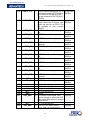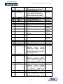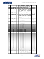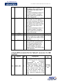
1
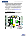
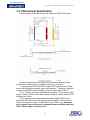
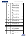
Your ePlatform Partner
User’s Manual for Advantech SOM-A2552 series module V1.00
User’s Manual
Of
Advantech RISC SOM-A2552 Series Module
System Module with Intel XScale PXA255 processor, SMI SM501
Graphic chip with Windows® CE.NET
Released Version:V1.00
Released Date: May. 19. 2004
Advantech Co., Ltd
Risc Embedded Computing Division
http://www.advantech.com/risc
Your ePlatform Partner
User’s Manual for Advantech SOM-A2552 series module V1.00
ABSTRACT
This manual describes the SOM-A2552 series module functions.
Copyright
This document is copyrighted, © 2003. All rights are reserved. The original manufacturer
reserves the right to make improvements to the products described in this document at any
time without notice.
No part of this document may be reproduced, copied, translated or transmitted in any
form or by any means without the prior written permission of the original manufacturer.
Information provided in this document is intended to be accurate and reliable. However, the
original manufacturer assumes no responsibility for its use, nor for any infringements upon the
rights of third parties that may result from such use.
Acknowledgements
IBM, PC/AT, PS/2 and VGA are trademarks of International Business Machines Corporation.
Intel® is trademark of Intel Corporation.
Microsoft® Windows® CE.NET is a registered trademark of Microsoft Corp.
All other product names or trademarks are properties of their respective owners.
For more information on this and other Advantech products please visit our
website at:
http://www.advantech.com
http://www.advantech.com/risc
For technical support and service for please visit our support website at:
http://eservice.advantech.com.tw/eservice/
Or directly mail to Advantech RISC platform application engineer:
[email protected]
Advantech RISC SOM design-in member can login-in the Advantech SOM
Design-in Zone for professional & real-time technical support & service:
http://risc-designin.advantech.com.tw
PS. The RISC design-in zone web portal is only for SOM design-in member
only.
2
Your ePlatform Partner
User’s Manual for Advantech SOM-A2552 series module V1.00
Revision History
Version
V1.00
Date
Reason
2004.05.19
1st Official released version. (For
9696255201, 9696255801, 9696255F01
& 9696255F12)
3
Your ePlatform Partner
User’s Manual for Advantech SOM-A2552 series module V1.00
Chapter 1 SOM-A2552 series Architecture
1.1 Introduction
The SOM-A2552 is WinCE ready, compact size module platform with
SBC-function-level functionality that is emphasis at high performance VGA
capability that offers Ultra low power consumption with SXGA LCD, Dual
Display, Analogy VGA in/out put, Audio Interface into a compact 68x68x6.8mm
size module.
By the integration of Intel PXA-255 32-bit SoC and SMI SM-501 VGA
controller, SOM-A2552 is perfect for Multimedia, mobility, battery powered,
great heavy display base embedded Internet appliance or so called smart
embedded devices.
SOM-A2552 series Design highlight:
- WinCE.NET-ready platform as functional system engine
- SoC Intel XScale PXA255 & Companion Graphic Chip SMI SM501provide
complete SBC functionality & high performance Graphic function in a
module
- Pre-define I/O Ready bus thru SODIMM-200 interface
- Design-in package: Reference kit with full design-in documentation
- Advantech RISC WinCE builder offers friendly application migration
interface
- Low profit 68x68mm
SOM-A200 architecture
SOM-A255x series are based on Advantech SOM-A200 architecture to
design. SOM-A200 is Advantech RISC ultra-low power series SOM
architecture. The following block diagram is the SOM-A200 architecture.
4
Your ePlatform Partner
User’s Manual for Advantech SOM-A2552 series module V1.00
Based on SOM-A200 architecture to design, SOM-A255x series have two
kinds of PCB form factors.
l SOM-A2552 & SOM-A2558 series: 68mm x 68mm x 6.8mm
l SOM-A255F series: 68mm x 102mm x 6.8mm
SOM-A2552 benefit
The SOM-A2552 series are very compact (68mm x 68mm x 6.8mm) and
highly integrated system module. SOM-A2552 series products have a
standardized form factor and standardized connectors (DDR-SODIMM
Memory Connector and two 100-pin board-to-board connectors) that carry a
specified set of signals. This standardization allows users to create
application-specified User Solution Board (CSB) which can accept a variety of
present and future SOM-A200 series modules.
SOM-A2552 series include popular & common peripheral functions such
as serial ports, USB, etc. The CSB designer can optimize exactly how each of
these functions is physically implemented. Connectors can be placed precisely
where they are needed for the application, on a baseboard designed to
optimally fit the system configuration and layout.
A CSB design may be used with a range of SOM-A2552 modules. This
flexibility can be used to differentiate products at various price/ performance
points, or to design “future proof” systems that have a built-in upgrade path.
The modularity of an SOM-A2552 solution also insures against obsolescence
as computer technology continues to evolve. A properly designed SOM-A2552
CSB can be used with several successive generations of SOM-A2552
modules. An SOM-A2552 CSB design thus has many of the advantages of a
custom computer board design, but delivers better obsolescence protection,
greatly reduced engineering effort, and faster time to market.
Based embedded platform integrates both low-level hardware and
software design and is always agreed to require heavy R&D resources, huge
development effort, risk as well as long time to market lead-time. Moreover,
the fast develop RISC SoC technology and short product life that has been
challenging System Integrators how to make a right product development
approach while foreseeing the huge advantage & benefit by adopting
RISC-base solution.
SOM-A2552 series are an innovate platform architecture of
WinCE.NET-ready complete functional system in a low profit module with
SODIMM 200-pin unified I/O ready bus interface that is designed to fit into
application-specified User Solution Board (CSB) with easy, risk-less, robust,
fast implementation approach. Dual expansion interface and Pre-select
Embedded OS also are well integrated on module. OS Board Support
Package (BSP) and advantech own-develop system utility & tools are also
supported for an easy design-in business philosophy.
SOM-A2552 series is designed for
l Wireless broadband terminals: Wireless access to video/TV/DVD/PVR,
wireless access to broadband connection, digital picture viewer, remote
access to Internet/email, remote control of AV functions
5
Your ePlatform Partner
User’s Manual for Advantech SOM-A2552 series module V1.00
l
l
l
l
l
Smart display devices: Kiosks, small DTV, thin client, high end mobile
consumer devices, videoconferencing
Mobile, battery-powered device platforms with large display demand
Vehicle computing/telemetric platforms for navigation/entertainment
demands
Multimedia terminal device platforms with large display
Security surveillance platforms with digital or analog video input/output
SOM-A2552 series design-in package
The Design-in Kit package provides developer complete reference
design-in suit for application evaluation/ development and own Customer
Solution Board (CSB) development. It contains the needed information,
documentation and tools for starting their hands-on work as the followings
items:
l Target SOM (SOM-A2552-440B0): SOM-A2552 standard version
board.
SOM-A255x series Reference Carrier Board (RCB): Sample CSB
for developer reference. The board can be used in SOM-A255x
series board. (SOM-A255x means SOM-A2552, SOM-A2558 and
SOM-A2552)
l 64MB compact flash card : the CF card is empty without any file
inside.
l SOM-A255x series support CD : includes
- sample image & boot loader
- manuals & datasheets
- SOM-A255x series CSB design guide
- S/W utility(upgrade utility, testing utility)
- SOM-A255x series WinCE 4.2 BSP & SDK
- Application note
l Testing Set:
It is designed for sample CSB or user own CSB/mass production test.
It includes:
H/W testing tools: RS232 loop-back testing tool, ADAM-4520
for RS485 testing, null MODEM cable, JTAG cable, USB
ActiveSync cable, Audio cable, RS232 cable and RS485
cable.
S/W testing Utility: Advantech-developed testing Utility. Testing
process will be implemented by S/W testing Utility and H/W
testing tools.
Document: “User's manual of SOM-A255x series testing kit”.
User can base on the documents to know how to implement
testing process.
l Software Development Tools:
Software tools is the complete package for user developed their
target image to align with their target CSB and applications
- BSP: Binary Board Support Package of target SOM Design-in Kit.
User can integrate their target WinCE platform in components &
Apps & drivers
- SDK: For user target Apps development
6
Your ePlatform Partner
User’s Manual for Advantech SOM-A2552 series module V1.00
-
Reference Image: Reference Image for the selected model of
SOM.
Bootloader: Bootloader for the SOM-A255x series board.
Upgrade Utility: User can use Upgrade utility to upgrade boot
logo, image & bootloader.
Except the Design-in package, Advantech also supply many types of LCD
kits for users to reduce their developing effort. The LCD kit include the
following items :
l LCD
l Inverter
l Cables: includes LCD signals cable, Inverter signals cable.
l Document: The LCD kit installation guide.
Advantech supply the following LCD kits for user to choose
l LCD-A057-STQ1-0 (Optional item)
5.7” STN QVGA LCD kit. The kit includes 5.7” STN QVGA LCD
(NAN-YA/ LCBFBTB61M23), 4-wires resistive T/S, inverter, cables
and installation guide. SOM-A2552 & SOM-A255F series don’t
support 320*240 STN panel in this moment, if user have this kind of
requirement, please contact with [email protected] or
advantech regional sales for further support.
l LCD-A064-TTV1-0 (Optional item)
6.4” TFT VGA LCD kit. The kit includes 6.4” TFT VGA LCD
kit(PRIMEVIEW PD064VT2), 4-wires resistive T/S, inverter, cables
and installation guide. All SOM-A255x series support this LCD kit in
reference image.
l LCD-A104-TTS1-0 (Optional item)
10.4” TFT SVGA LCD kit. The kit includes 10.4” TFT SVGA LCD
(AUO/ G104SN03v2), 4-wires resistive T/S, inverter, cables and
installation guide. Only SOM-A255F & SOM-A2552 series can
support this LCD-out mode.
l LCD-A150-TTX2-0 (Optional item)
15” TFT XGA LCD kit. The kit includes 15” TFT XGA LCD (AUO/
M150XN07), 4-wires resistive T/S, inverter, cables and installation
guide. Only SOM-A255F & SOM-A2552 series can support this
LCD-out mode.
SOM-A2552 series design-in kit(SOM-ADK2552-B00) is not included
any LCD kit. If user needs LCD kit to evaluate, please order your suitable
size LCD kit.
Risc CE-Builder
SOM-A255x series all support the Advantech optional RISC CE-Builder by
which developers can manage the BSP for their own platform development
thru a friendly users interface over the web.
RISC CE-Builder Solution is constituted by two parts: Web Image Builder
and CE-TUner.
Web Image Builder offers developers an online image building
mechanism through a friendly user interface to remotely conduct low-level
7
Your ePlatform Partner
User’s Manual for Advantech SOM-A2552 series module V1.00
software and platform customization / integration for their target application
without knowing / using Microsoft Platform Builder. The image building
machine links to Advantech’s Board Support Package (BSP) library so
developers can leverage Advantech’s low-level software solution database.
CE-TUner is a powerful value-added system utility / tool suit for
developers easily and simply develop, validate and upgrade their own SW
platform solution. CE-Tuner helps users fine-tune their target SW image for
optimized performance, verify settings, and platform tests before the
production image is certified.
RISC CE-Builder is not included in Design-in kit. If you need more
information about it, please contact with [email protected] or
advantech regional sales for further support.
1.12
SOM-A2552 Block diagram
SOM-A2552 series bases on Dual-Chips design concept, SoC Intel
XScale PXA255 & Graphic chip SMI SM501. The Block diagram is as
following:
8
Your ePlatform Partner
User’s Manual for Advantech SOM-A2552 series module V1.00
SoC Intel XScale PXA255 introduction
Intel XScale PXA255 processor is continuing the advance in handheld
multimedia functionality.
PXA255 is Low power, high performance 32-bit Intel XScale® core-based
CPU (200, 300 and 400 MHz). The SoC is ARM Architecture v.5TE compliant.
0.18µ process for high core speeds at low power.
Intel® Media Processing Technology including 40-bit accumulator and 16-bit
SIMD to enhance audio/video decode performance.
In power field, Low Power and Turbo modes enables enhanced optimal
battery life. 32 KB data and 32 KB instruction caches, 2 KB Mini data cache for
streaming data.
About PXA255 I/O expansion function, Integrated Memory and
PCMCIA/Compact Flash Controller with 100 MHz Memory Bus, 16-bit or 32-bit
ROM/Flash/SRAM (six banks), 16-bit or 32-bit SDRAM, SMROM (four banks),
as well as PCMCIA and Compact Flash for added functionality and
expandability. System Control Module includes 17 dedicated general-purpose
interruptible I/O ports, real-time clock, watchdog and interval timers, power
management controller, interrupt controller, reset controller, and two on-chip
oscillators.
Peripheral Control Module offers 16 channel configurable DMA controller,
integrated LCD controller with unique DMA for fast color screen support,
Bluetooth** I/F, serial ports including IrDA, I2C, I2S, AC97, three UARTs(1 Full
H/W flow control), SPI and enhanced SSP, USB end point interface, and
MMC/SD Card Support for expandable memory and I/O functionality.
About Intel PXA255 SoC detail information, user could visit Intel web site
for more.
Enhance Graphic Chip SMI SM501 introduction
The SM501 is a Mobile System-on-a-Chip (MSOC™ ) device. This robust device
delivers high-performance video and 2D operation, providing a solution for embedded
mADKets. The SM501 also contains a wide variety of I/Os, such as analog RGB and
digital LCD Panel interfaces, an 8-bit parallel interface, USB, UART, IrDA, Zoom
Video, AC97 or I2S, SSP, PWM, and I2C interfaces. These built-in functionalities help
to reduce overall system cost. Additional programmable GPIO bits can be used to
interface to external devices as well.
About SMI SM501 display chip detail information, user could visit SMI web
site for more.
System Memory
SOM-A2552 SDRAM can be configured as 4/8/16/32/64/128/256MB.
Users can base on their requirement to reconfigure the SDRAM size.
There are two functions Flash on SOM-A2552 series. One is Boot Flash,
the other is Storage Flash.
Boot Flash is 1MB NOR flash. In standard SOM-A2552 series product,
Advantech will pre-install the WinCE bootloader in it.
Storage Flash is used to save image & user APs. Storage Flash size is
also reconfigurable. The Storage Flash is M-system Flash. Storage Flash size
could be 0/16/32/64 MB. SOM-A2552 series have Multiple boot options
through the on-board Flash or Compact Flash Card (CFC) for easy maintain
and cost saving. If Storage Flash is 0MB that means user should put the image
in Compact Flash Card.
9
Your ePlatform Partner
User’s Manual for Advantech SOM-A2552 series module V1.00
CPLD
SOM-A2552 series have one CPLD on board. The CPLD take charges of
the following function:
l System memory assignments
l I/O control
l RTC control
Base on Advantech policy, Advantech won’t release the CPLD code to
user. In fact, when user designs their own target carrier board, they don’t need
to know the CPLD code. Advantech will release memory map of available
memory block and available GPIOs. These are fully enough to users to
develop their own carrier board.
1.2 System Specifications
The following table is SOM-A2552 series functional specifications.
SOM-A2552 standard product specification table
Model Name
Func.
CPU
Graphic Chip
System Memory(SDRAM)
Booting Flash
On-board Flash (Image &
Storage )
OS Image Storage
AMI Bus(X1 Bus)
Feature Extension
Bus(X2 Bus)
Watch Dog
RTC
System Backup battery
Serial Port
PCMCIA/Compact flash
I/F
USB Host
USB Client
SD/MMC
CRT-out
TV Interface
ZV port
LCD TTL Interface
Touch Screen Interface
SOM-A2552-440B0
Reconfiguration Option
PXA255-400MHz
SMI SM501 with 8MB embedded
SDRAM
64MB
200/300/400 MHz
SM501 with /without 8MB
embedded SDRAM
16/32/64/128 MB
1MB NOR Flash
-
0MB
0/16/32/64MB
WinCE.NET
100-pin B2B connector with driving
buffers
100-pin B2B connector (Provide ZV
& SD/MMC I/F)
PXA255 internal
Linux(By customer request)
External RTC w/backup power pin
Yes
RTC/SDRAM
-
3x Full RS-232 (TTL), 1x 2-wires
RS-232 (TTL),1x 3-wires
RS-232/RS-485
2 slots PCMCIA/CF or
1xPCMCIA, 1xCF
1x USB 1.1 Host
1x USB Client
Ix Ch(Support
Memory mode)
Up to 1280*1024
Yes
Yes
-
-
TV out
Yes
-
SM501 24 bit LCD interface,
resolution up to 1280*1024
-
4-wire resistive
Yes
10
Your ePlatform Partner
User’s Manual for Advantech SOM-A2552 series module V1.00
Audio Codec
Buzzer control
SM Bus Interface
AC’97 codec on board, support
Microphone-in, Line-in, Line-out
Speaker-out
Yes
Yes
-
Yes
-
H/W Reset, S/W Reset,
Suspend/Wake Up I/F
-
Power input
3.3V/5V
-
Operating temperature
0~60℃
System Reset
Operating humidity
Certification
Optional for -10~60℃ &
0%~90% relative humidity
-
FCC/CE
-
-20~80℃
Form factor
68mm*68mm*6.8mm
Ps.. “Reconfiguration Option” column provide users many choices. “-“means
no option. If standard product SOM-A2552-440B0’s spec. doesn’t fit user’s
requirement, user could contact with Advantech for SOM-A2552
reconfiguration.
* Advantech SOM-A255x series have wide temperature products. About detail product
information, user could visit website http://www.advantech.com.tw/epc/phoenix/ . User also
could contact with [email protected] or advantech regional sales for further
information.
SOM-A2552-440B0 is off-the-shelf standard product. Advantech welcome
SOM-A2552 re-configuration demand. Users could base on the column of
SOM-A2552 spec. to re-configurate userized SOM-A2552. “Reconfiguration
Option” column provide users many choices. “-“means no option. If standard
product SOM-A2552-440B0’s spec. doesn’t fit user’s requirement, user could
contact with Advantech for SOM-A2552 reconfiguration.
11
Your ePlatform Partner
User’s Manual for Advantech SOM-A2552 series module V1.00
1.2.1 Mechanical Specification
Following figure shows the mechanical drawing of SOM-A2552 series.
The above figure shows the SOM-A2552 mechanical drawing. Users
could follow the above figure to implement the layout procedure.
1st drawing shows the SOM-A2552 module PCB mechanical data. When
users enter the layout procedure, user could follow the 1st drawing to place the
connector. SOM-A2552 series PCB form factor is 68mm*68mm*68mm.
The 2nd drawing shows the PCB thickness limitation. The component side
height is 2.8mm, and the solder side maximum height is 3.00mm and the PCB
thickness is 1.00mm.
The 3rd drawing shows allied mechanical data of SOM-A2552 series
board and CSB. Users could see that the matting height is 3.00mm and the
solder side maximum height of SOM-A2552 is also 3.00mm. So, Advantech
don’t suggest users to place any components between SOM module and
CSB in layout stage. It could be short!
12
Your ePlatform Partner
User’s Manual for Advantech SOM-A2552 series module V1.00
Most users will question the height of SOM structure product. Does
product be too thick based on SOM structure product? User could see the
answer in the 3rd mechanical drawing. Maximum height of SOM module allied
with CSB is 5.20mm. One port USB 1.1 host connector height is 8.37mm, 1
DB-9 RS-232 connector is 12.53mm, 1 type-II CF slot is 8.72mm. So, this is
the answer! If users want to use any standard I/O connector on CSB, then
SOM structure is not the maximum height maker. The maximum highness is
decided by I/O connector, not SOM structure.
1.2.2 Power System Requirement
SOM-A2552 Operating DC value table
Symbol
Description
Min.
SYS_VCC3P SOM system DC 3.3V DC-in
3
power source
3
SOM system DC 5.0V DC-in
SYS_VCC
power source
4.5
Back-up power source for RTC &
BAT_VCC
SDRAM
Input DC Operating Conditions
Input High Voltage, all standard
VIH
input and I/O pins
0.8*VCC
Input Low Voltage, all standard
VIL
input and I/O pins
VSS
Output DC Operating Conditions
Output High Voltage, all standard
VOH
output and I/O pins
VCC-0.1
Output Low Voltage, all standard
VOL
output and I/O pins
VSS
Typ.
Max.
3.3
3.6
5.5
5.5
SYS_VC
C3P3
VCC
0.2*VCC
VCC
VSS+0.4
1.2.3 Power Consumption
In WinCE O.S. environment, SOM-A2552 series products have 3 kinds of
operating model :
l Normal mode: I/O and system all work well. All component on
SOM-A55x are powered.
l Idle mode: I/O and system all work well except backlight control
circuit. In order to do power-saving, LCD backlight control circuit
will disable the LCD backlight inverter.
l Suspend mode: all devices are no-powered except SDRAM,
RTC(real time clock) & some CPU(PXA255) power pins. In
suspend mode, SOM-A255x series are only powered by
BAT_VCC pin ( Li-ion 3.0V coin battery from CSB).If user doesn’t
design coin battery to power BAT_VCC pin, then Suspend mode
doesn’t work on SOM-A55x series products.
About detail power consumption of every SOM-A255x series, please
contact with [email protected].
13
Your ePlatform Partner
User’s Manual for Advantech SOM-A2552 series module V1.00
Chapter 2 Assignments and Descriptions
2.1 Connector Locations
Figure SOM-A2552 series component side
Figure SOM-A2552 series solder side
Connector
AMI bus (X1)
SOM Connector vendor table
vendor
Matsushita electric works,
LTD.
14
PN
AXK600335
Your ePlatform Partner
User’s Manual for Advantech SOM-A2552 series module V1.00
SOM-R200 (X2)
Standard Golden finger
200-pin
Feature extension bus
Matsushita electric works,
(X3)
LTD.
JP1
PXA255 JTAG pin header
JP2
SOM CPLD JTAG port
PS.JP1 & JP2 are 2.00 mm 6*1 pin-headers.
CSB Mating Connector table
vendor
Matsushita electric works,
LTD.
SODIMM-200 (X2)
QUASAR SYSTEM INC.
Feature extension bus
Matsushita electric works,
(X3)
LTD.
Connector
AMI bus (X1)
AXK600335
-
PN
AXK500135
CA0075-200N31
AXK500135
Advantech RISC SOM-A200 ultra low power series (SOM-A2552,
SOM-A2558 and SOM-A255F) all follow the same pin definition in X1,X2 and
X3. So, users could design their own CSB to be compatible with all advantech
RISC ultra low power series SOM easily. In this way, users’CSB will be
powerful upgrade capability & option choice.
X1: AMI bus
AMI bus connector is PXA255 ARM bus. It includes complete system
address lines, data lines, GPIOs (for interrupt source) and Chip select pins
(nCS). Users could use this bus to extend any other IC controller on CSB to
implement the function which SOM modules not provide. In order to keep the
system bus signals well, every address lines and data lines are driven by
buffers. Buffers’signals direction controls are implemented by CPLD.
X2: SODIMM-200 connector
Most I/O functions fog in X2. X2 includes PCMCIA/CF, T/S, Audio, system
reset control, SOM system power input pins, I2C, USB host, USB client,
RS-232 ports, RS-485 port, LCD out, CRT out and PS/2 ports. Every I/O
functions will be described in the following content in detail.
X3: Feature Extension connector
Advantech SOM-A series products use dual-chip or triple-chip design
concepts. The companion chip’s I/O function will come out through the X3. In
SOM-A255F series, SD/MMC & ZV (zoom video) I/F are included in X3.
ADVANTECH SOM-A200 is a powerful and helpful architecture for users
to implement a RISC system. There are three types of interfaces. One is
SO-DIMM 200 gold finger interface and two 100-pin B2B connectors.
15
Your ePlatform Partner
User’s Manual for Advantech SOM-A2552 series module V1.00
Pin Definition
¦JP1
PXA255 JTAG pin header
Pin Num.
1
2
3
4
5
6
7
Description
TCK
TDI
TDO
TMS
nJTAGTRST
GND
nRESET
Note
Pin type
P : DC power pin or system ground pin
I : digital input pin
O : digital output pin
IO : bidirectional pin
AI : analog input pin
AO : analog output pin
- : no function
¦SODIMM-200 Pin Out Table (X2)
Pin
No.
1
2
3
4
5
6
7
8
9
10
11
12
13
14
15
16
17
18
19
20
21
22
23
Signals
SA_SKT_D0
SA_SKT_D8
SA_SKT_D1
SA_SKT_D9
SA_SKT_D2
SA_SKT_D10
SA_SKT_D3
SA_SKT_D11
SA_SKT_D4
SA_SKT_D12
SA_SKT_D5
SA_SKT_D13
SA_SKT_D6
SA_SKT_D14
SA_SKT_D7
SA_SKT_D15
SA_SKT_A14
SA_SKT_A15
SA_SKT_A12
SA_SKT_A13
SA_SKT_A10
SA_SKT_A11
SA_SKT_A8
Typ
e
AIO
IO
IO
IO
IO
IO
IO
IO
IO
IO
IO
IO
IO
IO
IO
IO
IO
IO
IO
IO
IO
IO
IO
Description
PCMCIA/CF data 0
PCMCIA/CF data 8
PCMCIA/CF data 1
PCMCIA/CF data 9
PCMCIA/CF data 2
PCMCIA/CF data 10
PCMCIA/CF data 3
PCMCIA/CF data 11
PCMCIA/CF data 4
PCMCIA/CF data 12
PCMCIA/CF data 5
PCMCIA/CF data 13
PCMCIA/CF data 6
PCMCIA/CF data 14
PCMCIA/CF data 7
PCMCIA/CF data 15
PCMCIA/CF address 14
PCMCIA/CF address 15
PCMCIA/CF address 12
PCMCIA/CF address 13
PCMCIA/CF address 10
PCMCIA/CF address 11
PCMCIA/CF address 8
16
Default state
No pulling
No pulling
No pulling
No pulling
No pulling
No pulling
No pulling
No pulling
No pulling
No pulling
No pulling
No pulling
No pulling
No pulling
No pulling
No pulling
No pulling
No pulling
No pulling
No pulling
No pulling
No pulling
No pulling
Your ePlatform Partner
User’s Manual for Advantech SOM-A2552 series module V1.00
24
25
26
27
28
29
30
31
32
33
34
35
36
37
38
39
40
SA_SKT_A9
SA_SKT_A6
SA_SKT_A7
SA_SKT_A4
SA_SKT_A5
SA_SKT_A2
SA_SKT_A3
SA_SKT_A0
SA_SKT_A1
SA_SKT_A16
SA_SKT_A17
SA_SKT_A18
SA_SKT_A19
SA_SKT_A20
SA_SKT_A21
SA_SKT_A22
nSA_SKT_IOR
IO
IO
IO
IO
IO
IO
IO
IO
IO
IO
IO
IO
IO
IO
IO
IO
O
41
42
SA_SKT_A24
XP
IO
AI
43
nSA_SKT_WE
O
44
YP
AI
45
nSA_SKT_IOW O
46
XN
AI
47
nSA_SKT_RE
G
O
48
YN
AI
49
50
51
52
SA_SKT_A23
GND
SA_SKT_A25
AC97_EAPD
IO
P
IO
O
53
nSA_SKT_OE
O
PCMCIA/CF address 9
PCMCIA/CF address 6
PCMCIA/CF address 7
PCMCIA/CF address 4
PCMCIA/CF address 5
PCMCIA/CF address 2
PCMCIA/CF address 3
PCMCIA/CF address 0
PCMCIA/CF address 1
PCMCIA/CF address 16
PCMCIA/CF address 17
PCMCIA/CF address 18
PCMCIA/CF address 19
PCMCIA/CF address 20
PCMCIA/CF address 21
PCMCIA/CF address 22
PCMCIA I/O read. Performs read
transactions from PCMCIA I/O
space.
PCMCIA/CF address 24
4-wires resistive touch screen
signals: X+ Position Input.
PCMCIA write enable. (output)
Performs writes to PCMCIA
memory and to PCMCIA attribute
space. Also used as the write
enable signal for Variable Latency
I/O.
4-wires resistive touch screen
signals: Y+ Position Input.
PCMCIA I/O write signal. (output)
Performs write transactions to
PCMCIA I/O space.
4-wires resistive touch screen
signals: X– Position Input
PCMCIA Register select. (output)
Indicates that the target address
on a memory transaction is
attribute space. Has the same
timing as the address bus.
4-wires resistive touch screen
signals: Y– Position Input
PCMCIA/CF address 23
Ground
PCMCIA/CF address 25
External audio Amplifier power
down control
PCMCIA output enable. (output)
Reads from PCMCIA memory and
17
No pulling
No pulling
No pulling
No pulling
No pulling
No pulling
No pulling
No pulling
No pulling
No pulling
No pulling
No pulling
No pulling
No pulling
No pulling
No pulling
No pulling
No pulling
No pulling
No pulling
No pulling
No pulling
No pulling
No pulling
No pulling
No pulling
No pulling
No pulling
No pulling
Your ePlatform Partner
User’s Manual for Advantech SOM-A2552 series module V1.00
54
55
56
57
58
59
60
61
62
63
64
65
66
67
68
69
70
71
72
73
74
75
76
77
78
to PCMCIA attribute space.
LINEOUT_R AO Audio line-Out right channel
nSA_SKT1_CD I PCMCIA/CF slot 0 card detect pin No pulling
1
LINEOUT_L AO Audio line-Out left channel
nSA_SKT0_CD I PCMCIA/CF slot 1 card detect pin No pulling
1
1.
AC97_LINEIN_ AI Audio line input right channel.
R
nSA_SKT1_CE O PCMCIA/CF slot 0 card enable pin No pulling
1
1.
AC97_LINEIN_ AI Audio line input left channel.
L
nSA_SKT0_CE O PCMCIA/CF slot 0 card enable pin No pulling
1
1.
MIC_IN
AI First Microphone input
nSA_SKT1_CE O PCMCIA/CF slot 1 card enable pin No pulling
2
2.
GND
P Ground
SA_SKT1_VCC P PCMCIA/CF slot 1 power pin
nSA_SKT0_VS I PCMCIA/CF slot 0 voltage sense Pull high with
1
pin 1.
10Kohm
nSA_SKT1_VS I PCMCIA/CF slot 1 voltage sense Pull high with
1
pin 1.
10Kohm
nSA_SKT0_CE O PCMCIA/CF slot 0 card enable pin No pulling
2
2.
SA_SKT1_RDY I PCMCIA/CF slot 1 ready pin.
Pull high with
10Kohm
SA_SKT0_RDY I PCMCIA/CF slot 0 ready pin.
Pull high with
10Kohm
nSA_SKT0_VS I PCMCIA/CF slot 0 voltage sense Pull high with
2
pin 2.
10Kohm
nSA_SKT1_VS I PCMCIA/CF slot 1 voltage sense Pull high with
2
pin 2.
10Kohm
SA_SKT0_RST O PCMCIA/CF slot 0 reset pin.
Pull high with
10Kohm
SA_SKT1_RST O PCMCIA/CF slot 1 reset pin.
Pull high with
10Kohm
nSA_SKT0_W I PCMCIA/CF slot 0 wait signals. Pull high with
AIT
Driven low by the PCMCIA card to 10Kohm
extend the length of the transfers
to/from the PXA255 processor.
nSA_SKT1_CD I PCMCIA/CF slot 1 card detect pin No pulling
2
2.
nSA_SKT1_W I PCMCIA/CF slot 1 wait signals.
Pull high with
AIT
Driven low by the PCMCIA card to 10Kohm
extend the length of the transfers
to/from the PXA255 processor.
nSA_SKT0_CD I PCMCIA/CF slot 0 card detect pin No pulling
18
Your ePlatform Partner
User’s Manual for Advantech SOM-A2552 series module V1.00
79
2
nSA_SKT0_IOI
S16
I
80
81
SA_SKT0_VCC P
nSA_SKT1_IOI I
S16
82
nSA_PWR_ON
I
83
nBATT_FALT
I
84
nSW_RESET
I
85
nVDD_FALT
I
86
nRESET_OUT
O
87
88
GND
PWR_EN
P
O
89
BAT_VCC
P
2.
IO Select 16. (input) Acknowledge Pull high with
from the PCMCIA card that the
10Kohm
current address is a valid 16 bit
wide I/O address.
PCMCIA/CF slot 0 power pin.
Powered
PCMCIA/CF slot 0 IO Select 16.
Pull high with
10Kohm
Acknowledge from the PCMCIA
card that the current address is a
valid 16 bit wide I/O address.
System suspend/wakeup input pin. Pull high with
Falling edge triggered.
10Kohm
Main Battery Fault. Signals that
Pull high with
main battery is low or removed.
100Kohm
Assertion causes PXA255
processor to enter sleep mode or
force an Imprecise Data Exception,
which cannot be masked. PXA255
processor will not recognize a
wakeup event while this signal is
asserted. Minimum assertion time
for nBATT_FAULT is 1 ms.
System software reset input pin.
Pull high with
Falling edge triggered.
10Kohm
VDD Fault. Signals that the main Pull high with
power source is going out of
100Kohm
regulation. nVDD_FAULT causes
the PXA255 processor to enter
sleep mode or force an Imprecise
Data Exception, which cannot be
masked. nVDD_FAULT is ignored
after a wakeup event until the
power supply timer completes
(approximately 10 ms). Minimum
assertion time for nVDD_FAULT is
1 ms.
Reset Out. Asserted when
No pulling
nRESET is asserted and deasserts
after nRESET is deasserted but
before the first instruction fetch.
nRESET_OUT is also asserted for
“soft” reset events: sleep,
watchdog reset, or GPIO reset.
Ground
Power Enable for the power
Pull high with
supply. (output) When negated, it 100Kohm
signals the power supply to
remove power to the core because
the system is entering sleep mode.
3.0V li-ion coin battery positive No pulling
19
Your ePlatform Partner
User’s Manual for Advantech SOM-A2552 series module V1.00
90
nRESET
I
91
nDC_IN
I
92
SYS_VCC
P
93
SYS_VCC3P3
P
94
SYS_VCC
P
95
SYS_VCC3P3
P
96
SMBUS_CLK
IO
97
SYS_VCC3P3
P
98
SMBUS_DAT
IO
99
SYS_VCC3P3
P
pole input pin.
System hardware reset input pin. Pull high with
Falling edge triggered. Hard reset. 10Kohm
(input) Level sensitive input used
to start the processor from a known
address. Assertion causes the
current instruction to terminate
abnormally and causes a reset.
When nRESET is driven high, the
processor starts execution from
address 0. nRESET must remain
low until the power supply is stable
and the internal 3.6864 MHz
oscillator has stabilized.
System DC input indicator pin.
Pull low with
When the pin is low, it means
1Kohm
system is powered by external DC
power source. If user target device
is not power by battery, use could
use this pin as GPIO. The pin
connects to SoC PXA255 GPIO16.
SOM system DC power 5V input pin. SYS_VCC should always be
powered by DC 5V even in sleep
mode.
SOM system DC power 3.3V input pin. SYS_VCC should always be
powered by DC 3.3V even in sleep
mode.
SOM system DC power 5V input pin. SYS_VCC should always be
powered by DC 5V even in sleep
mode.
SOM system DC power 3.3V input pin. SYS_VCC should always be
powered by DC 3.3V even in sleep
mode.
System Management Bus clock Pull high with
pin. The pin is implemented by 4.7Kohm
SoC PXA255 I2C bus.
SOM system DC power 3.3V input pin. SYS_VCC should always be
powered by DC 3.3V even in sleep
mode.
System Management Bus data pin. Pull high with
The pin is implemented by SoC
4.7Kohm
PXA255 I2C bus.
SOM system DC power 3.3V input pin. SYS_VCC should always be
powered by DC 3.3V even in sleep
20
Your ePlatform Partner
User’s Manual for Advantech SOM-A2552 series module V1.00
100
101
USB_CP
SYS_VCC3P3
IO
P
102
103
USB_CN
SYS_VCC3P3
IO
P
104
BUZZER_OUT
O
105
USB_LINK_5V
I
106
UART2_RTS
O
107
108
GND
UART2_DCD
P
I
109
UART3_DCD
I
110
UART2_DSR
I
111
UART3_DSR
I
112
UART2_TXD
O
113
UART3_RXD
I
114
UART2_RXD
I
115
UART3_RTS
O
mode.
USB Client Positive pin
No pulling
SOM system DC power 3.3V input Powered
pin. SYS_VCC should always be
powered by DC 3.3V even in sleep
mode.
USB Client Negative pin.
No pulling
SOM system DC power 3.3V input pin. SYS_VCC should always be
powered by DC 3.3V even in sleep
mode.
Buzzer-out control signals. User
No pulling
can use the pin to control buzzer
power pin.
USB client link status indicator pin. Pull low with
When the pin is high, it means
100Kohm
USB client port has been
plugged-in USB device.
UART2 Request-to-Send signal
Pull high with
pin. If user doesn’t need UART2
100Kohm
function, user could use this pin as
GPIO. The pin connects to SoC
PXA255 GPIO45.
Ground
UART2 data-Carrier-Detect signal Pull high with
pin.
100Kohm
UART3 data-Carrier-Detect signal Pull high with
pin.
100Kohm
UART2 Data-Set-Ready signal pin. Pull high with
100Kohm
UART3 Data-Set-Ready signal pin. Pull high with
100Kohm
UART2 Transmit signal pin. If user Pull high with
doesn’t need UART2 function, user 100Kohm
could use this pin as GPIO. The
pin connects to SoC PXA255
GPIO43.
UART3 Receive signal pin. If user Pull high with
doesn’t need UART3 function, user 100Kohm
could use this pin as GPIO. The
pin connects to SoC PXA255
GPIO46.
UART2 Receive signal pin. If user Pull high with
doesn’t need UART2 function, user 100Kohm
could use this pin as GPIO. The
pin connects to SoC PXA255
GPIO42.
UART3 Request-to-Send signal
Pull high with
pin.
100Kohm
21
Your ePlatform Partner
User’s Manual for Advantech SOM-A2552 series module V1.00
116
UART2_CTS
I
117
UART3_TXD
O
118
UART2_DTR
O
119
UART3_CTS
I
120
UART2_RI
I
121
UART3_DTR
O
122
UART3_RI
I
123
UART1_DSR
I
124
UART1_DCD
I
125
UART1_CTS
I
126
UART1_RXD
I
127
UART1_RTS
O
128
UART1_TXD
O
129
UART1_DTR
O
130
131
GND
UART1_RI
P
I
132
133
134
135
136
137
N.C.
N.C.
N.C.
N.C.
GND
VDD_ENA
P
O
138
139
N.C.
VEE_ENA
O
UART2 Clear-to-Send signal pin. If Pull high with
user doesn’t need UART2 function, 100Kohm
user could use this pin as GPIO.
The pin connects to SoC PXA255
GPIO44.
UART3 Transmit signal pin. If user Pull high with
doesn’t need UART3 function, user 100Kohm
could use this pin as GPIO. The
pin connects to SoC PXA255
GPIO47.
UART Data-Terminal-Ready signal Pull high with
pin.
100Kohm
UART3 Clear-to-Send signal pin. Pull high with
100Kohm
UART2 Ring Indicator signal pin. Pull high with
100Kohm
UART3 Data-Terminal-Ready
Pull high with
signal pin.
100Kohm
UART3 Ring Indicator signal pin. Pull high with
100Kohm
UART1 Data-Set-Ready signal pin. Pull high with
100Kohm
UART1 Data-Carrier-Detect signal Pull high with
pin.
100Kohm
UART1 Clear-to-Send signal pin. Pull high with
100Kohm
UART1 Receive signal pin.
Pull high with
100Kohm
UART1 Request-to-Send signal
Pull high with
pin.
100Kohm
UART1 Transmit signal pin.
Pull high with
100Kohm
UART1 Data-Terminal-Ready
Pull high with
signal pin.
100Kohm
Ground
UART Ring Indicator signal pin.
Pull high with
100Kohm
N.C. just float this pin.
N.C. just float this pin.
N.C. just float this pin.
N.C. just float this pin.
Ground
LCD power control signal. User
No pulling
can use this pin to control the LCD
logic power MOS switch to achieve
power-saving.
N.C. just float this pin.
STN LCD VEE power control
No pulling
signal. User can use this pin to
22
Your ePlatform Partner
User’s Manual for Advantech SOM-A2552 series module V1.00
control STN LCD VEE power MOS
switch to achieve power-saving.
- N.C. just float this pin.
O LCD back light inverter power
control signal. User can use this
pin to control the LCD backlight
inverter to achieve power-saving.
IO USB host port1 D- data line.
- N.C. just float this pin.
IO USB host port1 D+ data line.
- N.C. just float this pin.
- N.C. just float this pin.
- N.C. just float this pin.
I UART5 Receive signal pin.
140
141
N.C.
VBK_ENA
142
143
144
145
146
147
148
USB_N1
N.C.
USB_P1
N.C.
N.C.
N.C.
UART5_RXD
149
UART4_RXD
I
150
UART5_RTS
O
151
UART4_TXD
O
152
UART5_TXD
O
153
154
155
156
157
N.C.
N.C.
N.C.
N.C.
nVBRIR_INC
O
158
159
CRT_R
AO
nVBRIR_UnD O
160
161
162
163
CRT_G
VBRIR_CS
AO
O
CRT_B
AO
nVCONR_INC O
No pulling
No pulling
No pulling
Pull high with
100Kohm
UART5 Receive signal pin.
Pull high with
100Kohm
UART5
Data-Terminal-Ready Pull high with
signal pin.
100Kohm
UART4 Transmit signal pin.
Pull high with
100Kohm
UART5 Transmit signal pin.
Pull high with
100Kohm
N.C. just float this pin.
N.C. just float this pin.
N.C. just float this pin.
N.C. just float this pin.
One of LCD inverter backlight No pulling
brightness
control
signals.
nVBRIR_INC is used to increase
or decrease Wiper Control.
Advantech suggests to connect the
pin to DS1804 1st pin.
The red CRT output.
No pulling
One of LCD inverter backlight No pulling
brightness
control
signals.
nVBRIR_UnD is used be Up/Down
Control. Advantech suggests to
connect the pin to DS1804 2nd pin.
The Green CRT output.
No pulling
One of LCD inverter backlight No pulling
brightness
control
signals.
VBRIR_CS is used be chip select
pin. Advantech suggests to
connect the pin to DS1804 7th pin.
The blue CRT output.
No pulling
One of STN LCD contrast control No pulling
signals. nVCONR_INC is used be
increase/decrease Wiper Control
23
Your ePlatform Partner
User’s Manual for Advantech SOM-A2552 series module V1.00
164
165
CRT_HSYNC
VCONR_CS
AO
O
166
167
CRT_VSYNC
VCONR_UnD
AO
O
168
CRT_SDA
-
169
CRT_CLK
-
170
171
172
173
174
175
176
177
178
179
180
181
182
183
184
185
186
187
188
189
190
191
192
193
194
195
196
B0
B1
B2
B3
B4
B5
B6
B7
G0
G1
G2
G3
G4
G5
G6
G7
R0
R1
R2
R3
R4
R5
R6
R7
N.C.
N.C.
FLM_VSYNC
O
O
O
O
O
O
O
O
O
O
O
O
O
O
O
O
O
O
O
O
O
O
O
O
O
pin. Advantech suggests to
connect the pin to DS1804 1st pin.
Horizontal sync for the CRT.
No pulling
One of STN LCD contrast control No pulling
signals. VCONR_CS is used be
chip
select
pin.
Advantech
suggests to connect the pin to
DS1804 7th pin.
Vertical sync for the CRT.
No pulling
One of STN LCD contrast control No pulling
signals. VCONR_UnD is used be
Up/Down
Control.
Advantech
suggests to connect the pin to
DS1804 2nd pin.
Reserved for future use. User can Pull high with
connect the pin to CRT I2C data 4.71Kohm
pin or just float it.
Reserved for future use. User can Pull high with
connect the pin to CRT I2C clock 4.71Kohm
pin or just float it.
B0 in 24-bit TFT mode.
No pulling
B in 24-bit TFT mode.
No pulling
B in 24-bit TFT mode.
No pulling
B in 24-bit TFT mode.
No pulling
B in 24-bit TFT mode.
No pulling
B in 24-bit TFT mode.
No pulling
B in 24-bit TFT mode.
No pulling
B in 24-bit TFT mode.
No pulling
G in 24-bit TFT mode.
No pulling
G in 24-bit TFT mode.
No pulling
G in 24-bit TFT mode.
No pulling
G in 24-bit TFT mode.
No pulling
G in 24-bit TFT mode.
No pulling
G in 24-bit TFT mode.
No pulling
G in 24-bit TFT mode.
No pulling
G in 24-bit TFT mode.
No pulling
R in 24-bit TFT mode.
No pulling
R in 24-bit TFT mode.
No pulling
R in 24-bit TFT mode.
No pulling
R in 24-bit TFT mode.
No pulling
R in 24-bit TFT mode.
No pulling
R in 24-bit TFT mode.
No pulling
R in 24-bit TFT mode.
No pulling
R in 24-bit TFT mode.
No pulling
N.C. just float this pin.
N.C. just float this pin.
Flat Panel TFT Vertical Sync/STN No pulling
Frame Pulse. For TFT displays,
this output connects to the Vertical
24
Your ePlatform Partner
User’s Manual for Advantech SOM-A2552 series module V1.00
197
LP_HSYNC
O
198
199
GND
M_DE
P
O
200
SHCLK
O
Sync input of the LCD panel. For
STN displays, this output connects
to the Frame Clock input of the
LCD panel.
This output indicates the start of a
new frame of pixels. The panel
needs to reset its line pointers to
the top of the screen.
Flat Panel TFT Vertical Sync/STN No pulling
Frame Pulse. For TFT displays,
this output connects to the Vertical
Sync input of the LCD panel. For
STN displays, this output connects
to the Frame Clock input of the
LCD panel.
This output indicates the start of a
new frame of pixels. The panel
needs to reset its line pointers to
the top of the screen.
Ground
Flat Panel Display Enable. This No pulling
signal is used as a data enable
when the pixel clock needs to latch
pixel data.
Flat Panel Pixel Clock. The active No pulling
edge of FPCLK is programmable.
The LCD panel uses this clock
when loading pixel data into its
Line Shift register. This signal
connects to the TXCLK input of the
LVDS transmitter.
¦100-pin B2B connector Pin Out Table (X1 connector, For AMI
interface)
Pin
No.
B1
Signals
nBUF_CS2
Type
O
Description
Default
state
Static chip selects. Chip selects to
static memory devices such as ROM
and
Flash.
Individually
programmable in the memory
configuration registers. This pin can
Pull-high
be used with variable latency I/O
with 100K
devices. nBUF_CS2 directly connect
ohm
to SoC PXA255 nCS2. User could
use this pin as chip select pin to
control the solution IC on carrier
board. This pin is reserved for user
to use.
25
Your ePlatform Partner
User’s Manual for Advantech SOM-A2552 series module V1.00
A1
B2
A2
B3
A3
B4
A4
B5
A5
B6
ADDR15
ADDR14
ADDR13
ADDR12
ADDR11
ADDR10
ADDR9
ADDR8
ADDR24
ADDR25
O
O
O
O
O
O
O
O
O
O
A6
nBUF_OE
O
B7
ADDR20
O
A7
nBUF_WE
O
B8
ADDR22
O
A8
BUF_RD_nW
R
O
B9
GND
P
A9
BUF_RDY
I
B10
A10
B11
A11
B12
A12
B13
A13
B14
A14
B15
A15
B16
A16
B17
A17
DATA15
DATA14
DATA13
DATA12
DATA11
DATA10
DATA9
DATA8
DATA31
DATA30
DATA29
DATA28
DATA27
DATA26
DATA25
DATA24
IO
IO
IO
IO
IO
IO
IO
IO
IO
IO
IO
IO
IO
IO
IO
IO
B18
nBUF_SDRA
S
O
A18
nBUF_SDCS
0
O
SoC PXA255 system address 15
SoC PXA255 system address 14
SoC PXA255 system address 13
SoC PXA255 system address 12
SoC PXA255 system address 11
SoC PXA255 system address 10
SoC PXA255 system address 9
SoC PXA255 system address 8
SoC PXA255 system address 24
SoC PXA255 system address 25
Memory output enable pin. Connect
to the output enables of memory
devices to control data bus drivers.
SoC PXA255 system address 20
Memory write enable. Connect to the
write
enables of memory devices.
SoC PXA255 system address 22
Read/Write for static interface.
Signals that the current transaction
is a read or write.
Ground
Variable Latency I/O Ready pin.
Notifies the memory controller when
an external bus device is ready to
transfer data.
SoC PXA255 system data 15
SoC PXA255 system data 14
SoC PXA255 system data 13
SoC PXA255 system data 12
SoC PXA255 system data 11
SoC PXA255 system data 10
SoC PXA255 system data 9
SoC PXA255 system data 8
SoC PXA255 system data 31
SoC PXA255 system data 30
SoC PXA255 system data 29
SoC PXA255 system data 28
SoC PXA255 system data 27
SoC PXA255 system data 26
SoC PXA255 system data 25
SoC PXA255 system data 24
SDRAM RAS. Connect to the row
address strobe (RAS) pins for all
banks of SDRAM.
SDRAM CS for bank 0. Connect to
the chip select (CS) pin for SDRAM.
For
the
PXA255
processor
nBUF_SDCS0 can be Hi-Z.
26
No pulling
No pulling
No pulling
No pulling
No pulling
No pulling
No pulling
No pulling
No pulling
No pulling
No pulling
No pulling
No pulling
No pulling
No pulling
Pull high
with
100Kohm
No pulling
No pulling
No pulling
No pulling
No pulling
No pulling
No pulling
No pulling
No pulling
No pulling
No pulling
No pulling
No pulling
No pulling
No pulling
No pulling
No pulling
No pulling
Your ePlatform Partner
User’s Manual for Advantech SOM-A2552 series module V1.00
B19 BUF_DQM0
O
A19 BUF_DQM2
O
B20 BUF_DQM3
O
A20 nBUF_PWAIT
I
B21
BUF_SDCLK
1
O
A21
BUF_SDCKE
1
O
B22
A22
B23
A23
B24
A24
B25
A25
B26
A26
B27
A27
GND
ADDR0
ADDR1
ADDR2
ADDR3
ADDR4
ADDR5
ADDR6
ADDR7
ADDR16
ADDR17
ADDR18
P
O
O
O
O
O
O
O
O
O
O
O
SDRAM DQM for data byte 0.
Connect to the data output mask
enables (DQM) for SDRAM.
SDRAM DQM for data byte 2.
Connect to the data output mask
enables (DQM) for SDRAM.
SDRAM DQM for data byte 3.
Connect to the data output mask
enables (DQM) for SDRAM.
PCMCIA wait. (input) Driven low by
the PCMCIA card to extend the
length of the transfers to/from the
PXA255 processor.
SDRAM Clock 1. Connect SDCLK
[1] to the clock pins of SDRAM in
bank pairs 0/1. They are driven by
either the internal memory controller
clock, or the internal memory
controller clock divided by 2. At
reset, all clock pins are free running
at the divide by 2 clock speed and
may be turned off via free running
control register bits in the memory
controller. The memory controller
also provides control register bits for
clock division and deassertion of
each SDCLK pin. SDCLK[2:1]
control register assertion bits are
always deasserted upon reset.
SDRAM and/or Synchronous Static
Memory clock enable. Connect to
the clock enable pins of SDRAM. It is
deasserted
during
sleep.
BUF_SDCKE1 is always deasserted
upon reset. The memory controller
provides control register bits for
deassertion.
Ground
SoC PXA255 system address 0
SoC PXA255 system address 1
SoC PXA255 system address 2
SoC PXA255 system address 3
SoC PXA255 system address 4
SoC PXA255 system address 5
SoC PXA255 system address 6
SoC PXA255 system address 7
SoC PXA255 system address 16
SoC PXA255 system address 17
SoC PXA255 system address 18
27
No pulling
No pulling
No pulling
Pull high
with
100Kohm
No pulling
No pulling
(For
SOM-255F
is
BUF_SDC
KE1)
No pulling
No pulling
No pulling
No pulling
No pulling
No pulling
No pulling
No pulling
No pulling
No pulling
No pulling
Your ePlatform Partner
User’s Manual for Advantech SOM-A2552 series module V1.00
B28
A28
B29
A29
B30
A30
B31
A31
B32
A32
B33
A33
B34
A34
B35
A35
B36
A36
B37
ADDR19
ADDR21
ADDR23
DATA0
DATA1
DATA2
DATA3
DATA4
DATA5
DATA6
DATA7
DATA16
DATA17
DATA18
DATA19
DATA20
DATA21
DATA22
DATA23
O
O
O
IO
IO
IO
IO
IO
IO
IO
IO
IO
IO
IO
IO
IO
IO
IO
IO
A37
nBUF_SDCA
S
O
B38
nBUF_SDCS
2
O
A38 BUF_DQM1
O
BUF_SDCLK
2
O
A39 nBUF_IOIS16
I
B39
SoC PXA255 system address 19
SoC PXA255 system address 21
SoC PXA255 system address 23
SoC PXA255 system data 0
SoC PXA255 system data 1
SoC PXA255 system data 2
SoC PXA255 system data 3
SoC PXA255 system data 4
SoC PXA255 system data 5
SoC PXA255 system data 6
SoC PXA255 system data 7
SoC PXA255 system data 16
SoC PXA255 system data 17
SoC PXA255 system data 18
SoC PXA255 system data 19
SoC PXA255 system data 20
SoC PXA255 system data 21
SoC PXA255 system data 22
SoC PXA255 system data 23
SDRAM CAS. Connect to the
column address strobe (CAS) pins
for all banks of SDRAM.
SDRAM CS for banks 2. Connect to
the chip select (CS) pins for SDRAM.
For the PXA255 processor nSDCS0
can be Hi-Z, Nsdcs1-3 cannot.
SDRAM DQM for data bytes 1.
Connect to the data output mask
enables (DQM) for SDRAM.
SDRAM
Clock
2.
Connect
BUF_SDCLK[2] to the clock pins of
SDRAM in bank pairs 2/3. They are
driven by either the internal memory
controller clock, or the internal
memory controller clock divided by
2. At reset, all clock pins are free
running at the divide by 2 clock
speed and may be turned off via free
running control register bits in the
memory controller. The memory
controller also provides control
register bits for clock division and
deassertion of each SDCLK pin.
SDCLK[2:1]
control
register
assertion bits are always deasserted
upon reset.
IO Select 16. Acknowledge from the
PCMCIA card that the current
address is a valid 16 bit wide I/O
28
No pulling
No pulling
No pulling
No pulling
No pulling
No pulling
No pulling
No pulling
No pulling
No pulling
No pulling
No pulling
No pulling
No pulling
No pulling
No pulling
No pulling
No pulling
No pulling
No pulling
No pulling
No pulling
No pulling
Pull high
with
100Kohm
Your ePlatform Partner
User’s Manual for Advantech SOM-A2552 series module V1.00
B40 nBUF_PWE
O
A40 KEYPAD_IRQ
I
B41
-
N.C.
A41 PXA_GP7
IO
B42 EVA_IRQ
-
A42
C950_485_IR
Q
I
B43 LAN1_IRQ
I
A43 USB_IRQ
I
address.
PCMCIA write enable. Performs
writes to PCMCIA memory and to
PCMCIA attribute space. Also used No pulling
as the write enable signal for
Variable Latency I/O.
GPIO pin. Advantech default
function is used as matrix Keypad
IRQ. The pin directly connects to
PXA255 GPIO2 (L13 pin). If user No pulling
doesn’t use the matrix key pad
function, use can use this pin as
GPIO pin.
N.C. just float this pin.
No pulling
(For
GPIO pin. The pin directly connects
SOM-255F
to PXA255 GPIO7 (G15 pin). This
is
GPIO pin is available for user to use.
PXA_GPIO
7)
Advantech use this pin to control
companion chip as IRQ function.
The pin is not available for CSB
design
of
SOM-A2558
&
SOM-A255F platform. SOM-A2558
& SOM-A255F user must float this
pin. This pin is directly connected to
SoC PXA255 GPIO9(F12).
Advantech default function is used
as external 16C950 solution IC IRQ.
The pin directly connects to PXA255
GPIO10 (F7 pin). If user doesn’t No pulling
design 16C950 on CSB to expand
COM function, user could use this
pin as GPIO.
Advantech default function is used
as external LAN solution IC IRQ. The
pin directly connects to PXA255
GPIO17 (D12 pin). If user doesn’t No pulling
design the other LAN chip on CSB to
expand LAN function, user could use
this pin as GPIO.
Advantech default function is used
as external USB host solution IC
IRQ. The pin directly connects to
PXA255 GPIO27 (B9 pin). If user
No pulling
doesn’t design the other USB
solution chip on CSB to expand USB
host function, user could use this pin
as GPIO.
29
Your ePlatform Partner
User’s Manual for Advantech SOM-A2552 series module V1.00
B44 C954_IRQ
I
A44 PXA_GP81
IO
B45 PXA_GP82
IO
A45 PXA_GP83
IO
B46 PXA_GP84
IO
A46 nBUF_CS1
O
B47 nBUF_CS4
O
A47 nBUF_CS3
O
Advantech default function is used
as external 16C954 solution IC IRQ.
The pin directly connects to PXA255
GPIO32 (A16 pin). If user doesn’t
design 16C950 on CSB to expand
COM function, user could use this
pin as GPIO.
GPIO pin. The pin directly connects
to PXA255 GPIO81 (F16 pin). This
GPIO pin is available for user to use.
GPIO pin. The pin directly connects
to PXA255 GPIO82 (E16 pin). This
GPIO pin is available for user to use.
GPIO pin. The pin directly connects
to PXA255 GPIO83 (E15 pin). This
GPIO pin is available for user to use.
GPIO pin. The pin directly connects
to PXA255 GPIO84 (D16 pin). This
GPIO pin is available for user to use.
Static chip selects. Chip selects to
static memory devices such as ROM
and
Flash.
Individually
programmable in the memory
configuration registers. nBUF_CS1
can be used with variable latency I/O
devices. Advantech default uses this
pin as storage flash chip select pin. If
no special application, Advantech
strongly suggest user to open this
pin in CSB.
Static chip selects. Chip selects to
static memory devices such as ROM
and Flash. Individually. nBUF_CS4
can be used with variable latency I/O
devices.
Advantech default use this pin as
companion chip chip select pin.
nBUF_CS4 pin is used for
EVA-C210 on SOM-A255F &
SOM-A2552 series. If no special
application,
Advantech
strongly
suggest user to open this pin in CSB.
Static chip selects. Chip selects to
static memory devices such as ROM
and Flash. Individually
programmable in the memory
configuration registers. nBUF_CS3
can be used with variable latency I/O
devices.
Advantech uses the pin as I/O
30
No pulling
No pulling
No pulling
No pulling
No pulling
Pull high
with
100Kohm
Pull high
with
100Kohm
Pull high
with
100Kohm
Your ePlatform Partner
User’s Manual for Advantech SOM-A2552 series module V1.00
B48 nBUF_CS5
O
A48 DMA_REQ1
I
B49 MBREQ
I
A49 DMA_ACK1
O
memory
block.
About
detail
description,
please
reference
“SOM-A255x series Memory and
Interrupt Map”.
Static chip selects. Chip selects to
static memory devices such as ROM
and
Flash.
Individually
programmable in the memory
configuration registers. nBUF_CS5
can be used with variable latency I/O
Pull high
devices.
with
Advantech default uses the pin as
100Kohm
display chip chip select pin.
nBUF_CS4 pin is used for SM501 on
SOM-A2552 & SOM-A255F series. If
no special application, Advantech
strongly suggest user to open this
pin in CSB.
Channel 1 DMA Request. Notifies
the DMA Controller that an external
device requires a DMA transaction. If
user wants to design a controller in
CSB with DMA mode, please check Pull low
with [email protected] first. with 1Kohm
If use doesn’t want to use this pin as
DMA_REQ, use could use the pin as
GPIO. The pin connects to SoC
PXA255 GPIO19.
Memory Controller alternate bus
master request. Allows an external
device to request the system bus
from the Memory Controller. If user
wants to design a controller in CSB
Pull low
with this pin function, please check
with 1Kohm
with [email protected] first.
If use doesn’t want to use this pin as
DMA_REQ, use could use the pin as
GPIO. The pin connects to SoC
PXA255 GPIO14.
Channel 1 DMA acknowledge.
Notifies an external device that it has
been acknowledged the DMA
controller. If user wants to design a
controller in CSB with DMA mode,
please
check
with No pulling
[email protected] first.
If use doesn’t want to use this pin as
DMA_ACK, use could use the pin as
GPIO. The pin connects to SoC
PXA255 GPIO22.
31
Your ePlatform Partner
User’s Manual for Advantech SOM-A2552 series module V1.00
B50 MBGNT
O
A50 3M6864
O
Memory Controller grant. Notifies an
external device that it has been
granted the system bus. If user
wants to design a controller in CSB
with this pin function, please check Pull low
with [email protected] first. with 1Kohm
If use doesn’t want to use this pin as
MBGNT, use could use the pin as
GPIO. The pin connects to SoC
PXA255 GPIO13.
3.6864 MHz clock. Output from
No pulling
3.6864 MHz oscillator.
¦ 100-pin B2B connector Pin Out Table (X3 connector for PCI, ZV port,
MMC interface and Misc. function)
Pin
No.
B1
A1
B2
A2
B3
A3
B4
A4
B5
A5
B6
A6
B7
A7
B8
A8
B9
A9
B10
A10
B11
A11
B12
A12
B13
A13
B14
A14
B15
Signals
N.C.
N.C.
N.C.
N.C.
N.C.
N.C.
N.C.
N.C.
N.C.
N.C.
N.C.
N.C.
N.C.
N.C.
N.C.
N.C.
N.C.
N.C.
GND
N.C.
N.C.
N.C.
N.C.
N.C.
N.C.
N.C.
N.C.
GND
N.C.
Typ
e
P
P
-
Model
N.C. just float this pin.
N.C. just float this pin.
N.C. just float this pin.
N.C. just float this pin.
N.C. just float this pin.
N.C. just float this pin.
N.C. just float this pin.
N.C. just float this pin.
N.C. just float this pin.
N.C. just float this pin.
N.C. just float this pin.
N.C. just float this pin.
N.C. just float this pin.
N.C. just float this pin.
N.C. just float this pin.
N.C. just float this pin.
N.C. just float this pin.
N.C. just float this pin.
Ground
N.C. just float this pin.
N.C. just float this pin.
N.C. just float this pin.
N.C. just float this pin.
N.C. just float this pin.
N.C. just float this pin.
N.C. just float this pin.
N.C. just float this pin.
Ground
N.C. just float this pin.
32
Default state
-
Your ePlatform Partner
User’s Manual for Advantech SOM-A2552 series module V1.00
A15
B16
A16
B17
A17
B18
A18
B19
A19
B20
A20
B21
A21
B22
A22
B23
A23
B24
A24
B25
A25
B26
A26
B27
A27
B28
A28
B29
A29
B30
A30
B31
A31
B32
A32
B33
A33
B34
A34
B35
N.C.
N.C.
N.C.
N.C.
N.C.
GND
N.C.
N.C.
GND
N.C.
N.C.
N.C.
N.C.
N.C.
N.C.
N.C.
N.C.
N.C.
N.C.
N.C.
N.C.
N.C.
N.C.
N.C.
N.C.
N.C.
N.C.
N.C.
N.C.
N.C.
N.C.
N.C.
N.C.
N.C.
N.C.
N.C.
N.C.
N.C.
N.C.
nMMCD
A35
MMCLK
P
P
-
N.C. just float this pin.
N.C. just float this pin.
N.C. just float this pin.
N.C. just float this pin.
N.C. just float this pin.
Ground
N.C. just float this pin.
N.C. just float this pin.
Ground
N.C. just float this pin.
N.C. just float this pin.
N.C. just float this pin.
N.C. just float this pin.
N.C. just float this pin.
N.C. just float this pin.
N.C. just float this pin.
N.C. just float this pin.
N.C. just float this pin.
N.C. just float this pin.
N.C. just float this pin.
N.C. just float this pin.
N.C. just float this pin.
N.C. just float this pin.
N.C. just float this pin.
N.C. just float this pin.
N.C. just float this pin.
N.C. just float this pin.
N.C. just float this pin.
N.C. just float this pin.
N.C. just float this pin.
N.C. just float this pin.
N.C. just float this pin.
N.C. just float this pin.
N.C. just float this pin.
N.C. just float this pin.
N.C. just float this pin.
N.C. just float this pin.
N.C. float this pin.
N.C. float this pin.
SD/MMC interface card detect pin. Pull high with
100Kohm
If user doesn’t need MMC/SD
I function, user could use this pin as
GPIO. The pin connects to SoC
PXA255 GPIO12.
MMC clock. Clock signal for the
No pulling
MMC Controller. If user doesn’t
O need MMC/SD function, user could
use this pin as GPIO. The pin
connects to SoC PXA255 GPIO6.
33
Your ePlatform Partner
User’s Manual for Advantech SOM-A2552 series module V1.00
B36
MMDAT3/
MMCCS0
A36
MMCMD
B37
MMDAT0
A37
B38
A38
B39
A39
B40
N.C.
N.C.
N.C.
N.C.
N.C.
ZV15
A40
ZV14
B41
ZV13
A41
ZV12
B42
ZV11
A42
ZV10
B43
ZV9
A43
ZV8
B44
ZV7
Chip select pin for MMC controller. No pulling (For
If user doesn’t need MMC/SD
SOM-255F is
O function, user could use this pin as MMCCS0)
GPIO. The pin connects to SoC
PXA255 GPIO8.
Multimedia Card Command.
Pull high with
IO
10Kohm
Multimedia Card Data pin.
Pull high with
10Kohm (For
IO
SOM-255F is
MMCDAT)
- N.C. float this pin.
- N.C. float this pin.
- N.C. float this pin.
- N.C. float this pin.
- N.C. float this pin.
16-bit R[4] video pixel input for
No pulling
RGB
I
5:6:5 mode or Y[7] video pixel input
for YUV 4:2:2 mode.
16-bit R[3] video pixel input for
No pulling
RGB
I
5:6:5 mode or Y[6] video pixel input
for YUV 4:2:2 mode.
16-bit R[2] video pixel input for
No pulling
RGB
I
5:6:5 mode or Y[5] video pixel input
for YUV 4:2:2 mode.
16-bit R[1] video pixel input for
No pulling
RGB
I
5:6:5 mode or Y[4] video pixel input
for YUV 4:2:2 mode.
No pulling
16-bit R[0] video pixel input for
RGB
I
5:6:5 mode or Y[3] video pixel input
for YUV 4:2:2 mode.
16-bit G[5] video pixel input for
No pulling
I RGB 5:6:5 mode or Y[2] video pixel
input for YUV 4:2:2 mode.
16-bit G[4] video pixel input for
No pulling
I RGB 5:6:5 mode or Y[1] video pixel
input for YUV 4:2:2 mode.
16-bit G[3] video pixel input for
No pulling
I RGB 5:6:5 mode or Y[0] video pixel
input for YUV 4:2:2 mode.
16-bit G[2] video pixel input for
No pulling
RGB 5:6:5 mode, U[7] video pixel
I
input for YUV 4:2:2 mode, or V[7]
video pixel input for YUV 4:2:2
34
Your ePlatform Partner
User’s Manual for Advantech SOM-A2552 series module V1.00
A44
ZV6
B45
ZV5
A45
ZV4
B46
ZV3
A46
ZV2
B47
ZV1
A47
ZV0
B48
A48
SDAZV
SCLZV
B49
VPHREF
A49
B50
GND
VPVSYNC
mode.
16-bit G[1] video pixel input for
No pulling
RGB 5:6:5 mode, U[6] video pixel
I input for YUV 4:2:2 mode, or V[6]
video pixel input for YUV 4:2:2
mode.
16-bit G[0] video pixel input for
No pulling
RGB 5:6:5 mode, U[5] video pixel
I input for YUV 4:2:2 mode, or V[5]
video pixel input for YUV 4:2:2
mode.
16-bit B[4] video pixel input for
No pulling
RGB 5:6:5 mode, U[4] video pixel
I input for YUV 4:2:2 mode, or V[4]
video pixel input for YUV 4:2:2
mode.
No pulling
16-bit B[3] video pixel input for
RGB 5:6:5 mode, U[3] video pixel
I input for YUV 4:2:2 mode, or V[3]
video pixel input for YUV 4:2:2
mode.
No pulling
16-bit B[2] video pixel input for
RGB 5:6:5 mode, U[2] video pixel
I input for YUV 4:2:2 mode, or V[2]
video pixel input for YUV 4:2:2
mode.
No pulling
16-bit B[1] video pixel input for
RGB 5:6:5 mode, U[1] video pixel
I input for YUV 4:2:2 mode, or V[1]
video pixel input for YUV 4:2:2
mode.
No pulling
16-bit B[0] video pixel input for
RGB 5:6:5 mode, U[0] video pixel
I input for YUV 4:2:2 mode, or V[0]
video pixel input for YUV 4:2:2
mode.
TV-in control serial data
Pull high with
IO
input/output (I2C-bus).
4.71Kohm
TV-in control serial clock output
Pull high with
O
(I2C-bus)
4.71Kohm
Horizontal Sync. A falling or rising
No pulling
edge on this input indicates the
I
end of the current scan line and the
beginning of the next.
P Ground
Vertical Sync. A rising or falling
No pulling
edge on
I this input indicates the end of the
current capture field and the
beginning
35
Your ePlatform Partner
User’s Manual for Advantech SOM-A2552 series module V1.00
A50
VPCLK
I
of the next one. The state of
VPHSYNC
determines whether the current
capture
field is ODD (VPHREF is High on
the
active edge of VPVSYNC) or
EVEN
(VPHREF is Low on the active
edge of
VPVSYNC).
Pixel Clock. VPCLK is the
reference clock for data on the
ZV[31:0] video pixel bus.
No pulling
2.2 function description
2.2.1 System Bus
System Bus includes PXA255 address bus, data bus, memory control
signals and GPIOs.
System Bus enters CSB by X1. In order to make sure that system bus
signals have perfect electrical waves, System Bus signals are driven by buffers
to enhance signals performance.
Data Bus
PXA255
Address Bus
Strengthed Data Bus
Buffers
Buffers
Buffers
Strengthed Address Bus
X1 conn.
Strengthed Memory Control
signals
Memory Control
signals
The buffers signals direction control is control by CPLD on SOM-A255x
module.
2.2.2 COM
SOM-A255x series (SOM-A2552, SOM-A2558, SOM-A255F) all support 5
x RS-232 ports: 3 full function (FF) RS-232 ports, 1x 2-wire (RX, TX) RS-232
and 1x 3-wire (RX, TX, RTS) RS-232 port. COM port function assignments are
as following:
Ø COM1: FF RS-232
Ø COM2: FF RS-232
Ø COM3: FF RS-232
Ø COM4: 2-wire (RX, TX) RS-232
Ø COM5: 3-wire (RX, TX, RTS) RS-232
All RS-232 ports are TTL levels.
36
Your ePlatform Partner
User’s Manual for Advantech SOM-A2552 series module V1.00
According to user target CSB demand, user could define COM5 as 3-wire
(RX, TX, RTS) RS-232 port or pass through RS-485 transceiver to act as
RS-485 function. User could references “Advantech SOM-A255x series CSB
design guide “to design the COM5.
2.2.3 USB 1.1 Host
SOM-A255F & SOM-A2558 series supports 2 USB host ports.
SOM-A2552 series supports 1 USB host port. The USB host ports on the
SOM-A255x are USB 1.1 compatible. The default Windows CE.NET and Linux
on board support USB keyboards, mice and mass storage devices. User could
check the " SOM-A255x series verified compatible peripherals list " to know the
verified compatible peripherals. If user wants to connect other devices, it may
take customization on the Windows CE.
2.2.4 USB 1.1 client
The USB client port on the SOM-A255x is USB 1.1 compatible. USB client
connector is used to communicate with master device (ex: PC) for ActiveSync.
About SOM-A255x series ActiveSync installation, please reference to
“Installation Guide-Advantech RISC platform with Microsoft ActiveSync 3.7”.
2.2.5 T/S
SOM-A255x series supports 4-wires (X+, X-, Y+, Y-) resistive T/S
interface.
2.2.6 PCMCIA/CF
All SOM-A255x series supports 2 PCMCIA interface (I/F) or 2 CF I/F or 1
PCMCIA & 1 CF I/F. User could check “ SOM-A255x Series Carrier Board
Design Guide “ to know how to design the I/F.
PCMCIA/CF I/F power control circuit is designed on SOM module, so
PCMCIA/CF I/F is hot-swappable.
Advantech strongly suggest user to design one CF or one PCMCIA
slot on user’s target carrier board, even user doesn’t need this port in
target product. Advantech platform always use CF or PCMCIA slot to be
system S/W upgrading port. If user doesn’t design 1 CF or PCMCIA slot
on carrier board, user will run into trouble when user wants to upgrade
image, boot loader & boot-logo.
2.2.7 SD/MMC
All SOM-A255x series supports 1 slot SD/MMC port. The Multi Media
Card (MMC) is a low cost data storage and communication media. The MMC
controller in the SOM-A255x is compliant with The Multi Media Card System
Specification, Version 2.1. The only exception is one and three byte data
transfers are not supported.
SD/MMC I/F in SOM-A255x only support 1-bit memory mode, not support
I/O mode.
2.2.8 Audio (AC’97 Codec on board)
All SOM-A255x uses Realtek ALC202 AC97 audio Codec on SOM
module. SOM-A255x series provides mono microphone-in, stereo line-in, and
37
Your ePlatform Partner
User’s Manual for Advantech SOM-A2552 series module V1.00
stereo line-out interface. If users want to drive speakers, users could follow the
“Advantech SOM-A255x series CSB design guide “to design the audio
amplifier on CSB.
2.2.9 CRT-out
SOM-A255F & SOM-A2552 series supplies CRT-out I/F which resolution
is up to 1024*768. CRT-out function comes from SM501. CRT-out signals are
all analog signals; user must follow the analog signals layout rules.
SOM-A2558 series doesn’t support CRT-out function, but user could
design CRT-out solution IC on CSB to add the function on SOM-A2558
platform. About detail implement way, please check “Advantech SOM-A255x
series CSB design guide “.
2.2.10 LCD TTL interface w/LCD Brightness & Contrast Control
interface
SOM-A2552 & SOM-A255F series LCD-out interface comes from SM501.
SOM-A2552 & SOM-A255F LCD-out supports 24 bit and resolution up to
1024*768. SOM-A2552 & SOM-A255F supports both active and passive LCD
displays. SOM-A2558 series LCD-out function comes from SoC PXA255.
SOM-A2558 LCD-out supports 16 bit and resolution up to 800*600.
The LCD signals are 3.3V level in X2. If users’CSB want to drive 5V level
panel, users could design buffers on CSB to translate LCD signals level. User
could refer “Advantech SOM-A255x series CSB design guide “.
Advantech design LCD brightness control circuit & LCD contrast control
circuit on SOM-A255x series modules. STN LCD panel needs contrast control
signals. In X2, LCD contrast control signals are nVCONR_INC, VCONR_CS
and VCONR_UnD. The control signals are based on DALLAS DS1804 NV
Trimmer Potentiometer to design. Users could check the “Advantech
SOM-A255x series CSB design guide “ to know how to wire. User could check
“to know how to control.
Brightness control signals are used to control the LCD backlight inverter
lamp current. In X2, LCD brightness control signals are nVBRIR_INC,
VBRIR_CS and nVBRIR_UnD. The control signals are based on DALLAS
DS1804 NV Trimmer Potentiometer to design. Users could check the
“Advantech SOM-A255x series CSB design guide “to know how to wire. User
could check appendix about SOM-A255F memory map to know how to control.
If user wants to connect CSB to LVDS type LCD, user could reference
“Advantech SOM-A255x series CSB design guide “to design LVDS
Transmitter on CSB. SOM-A255x series only support 1 channel LVDS LCD
panel.
The sample images of SOM-A2552, SOM-A255F series could support 4
kinds of display modes:
l 320x240 TFT: In SOM-A2552 & SOM-A255F module, user
CAN’T verify the performance by Advantech LCD kit
LCD-A057-STQ1-0. Because SOM-A2552 & SOM-A255F
supports 320x240 TFT mode, but LCD-A057-STQ1-0 is 320x240
STN panel.
l 640x480 TFT: user could verify the performance by Advantech
LCD kit LCD-A064-TTV1-0.
38
Your ePlatform Partner
User’s Manual for Advantech SOM-A2552 series module V1.00
l
800x600 TFT: user could verify the performance by Advantech
LCD kit LCD-A104-TTS1-0.
l 1024x768 TFT: user could verify the performance by Advantech
LCD kit LCD-A150-TTX2-0.
Except 320x240 TFT mode, user could verify the LCD-out function by
Advantech LCD kit. Advantech LCD kit LCD-A057-STQ1-0 is 320x240 STN
type LCD, not TFT type, so user couldn’t verify the 320x240 TFT function by
sample images.
The sample images of SOM-A2558 series could support 4 kinds of display
modes:
l 320x240 STN: User can use Advantech LCD kit
LCD-A057-STQ1-0 to evaluate the LCD-out performance of
SOM-A2558 platform.
l 640x480 TFT: User can use Advantech LCD kit
LCD-A064-TTV1-0 to evaluate the LCD-out performance of
SOM-A2558 platform.
2.2.11 Zoom Video (ZV) port
SOM-A255F & SOM-A2552 series ZV port comes from SM501.
SOM-A2558 series don’t support the function. ZV Port can interface with video
decoders, such as NTSC/PAL decoders, MPEG-2 decoders, and JPEG Codec.
The ZV Port supports resolutions up to 1280x1024. It directly accepts digitized
RGB or YUV signals, and does not accept analog signals.
In 16-bit mode, the ZV [15:8] signals are the most-significant eight video
pixel inputs. In 8-bit mode, these signals are not used. In 16-bit mode, the ZV
[7:0] signals are the least-significant eight video pixel inputs. In 8-bit mode,
these signals are the only eight video pixel inputs.
About how to wire the ZV port with NTSC/PAL decoders, please check
“Advantech SOM-A255x series CSB design guide “.
2.2.12 System Reset Interface
SOM-A255x series all supply 3 kinds of System reset interface as
following:
Ø nRESET : hardware reset input pin. The pin is pulled high in
SOM-A255F. The pin is triggered by signal falling edge.
Ø nSW_RESET : software rest input pin. The pin is pulled high in
SOM-A255F. The pin is triggered by signal falling edge.
Ø nSA_PWR_ON : Suspend/wake-up pin. The pin is pulled high in
SOM-A255F. The pin is triggered by signal falling edge.
2.2.13 Buzzer Control Interface
SOM-A255x series all support this function. Buzzer-out control signal is
designed to control the buzzer on/off status.
If users want to design buzzer on CSB to be reminding or alarm system,
user could reference “Advantech SOM-A255x series CSB design guide “.
If users want to control the buzzer, users can check the memory map to
do it.
39
Your ePlatform Partner
User’s Manual for Advantech SOM-A2552 series module V1.00
2.2.14 System Management Bus (SM Bus) interface
SOM-A255x series SM Bus is implemented by PXA255 I2C bus. If users’CSB is
powered by battery pack with SM bus battery gauge IC, then users could connect the
SOM-A255x SM Bus to battery pack to monitor battery status. SOM-A255x series SM
bus directly support TI BQ2040 gas gauge IC.
2.2.15 Power-input
SOM-A255x needs 3.3V & 5V DC power inputs. The power sources (3.3V,
5V) must always be supplied even in system sleep mode. SOM-A255x power
management is completely implemented on itself; users’CSB doesn’t need to
control the power supply to SOM-A255x.
2.2.16 Back-up power input
If user want to keep the real time clock(RTC) works well in power off mode,
user should connect the coin battery positive pin to BAT-VCC in X2
directly .The back-up power pin (BAT_VCC) is the only power source to supply
RTC power when SOM-A255x system power (3.3V, 5V) is off.
The coin battery must be 3.0V Li-ion coin type.
The coin battery charging circuit is designed on SOM-A255x, so user
shouldn’t and needn’t design the charging circuit on CSB.
If users don’t need RTC function in CSB, just let the BAT_VCC pin open.
2.2.17 PCI I/F (Thru X3)
SOM-A2558 & SOM-A255F could support 4 channels PCI device
controllers on CSB. The PCI clock is 33 MHz. PCI I/F comes from Advantech
EVA-C210 I/O enhancement chip. The PCI I/F feature is as followings:
-
Compatible with PCI specification version 2.2
-
32-bit data bus interface
-
Built-in PCI bus arbiter
-
Supports up to 3 individual external bus master devices
-
Support PCI Bus Controller (FPCI) to PCI slave I/O read/write,
memory read/write, configuration read/write cycle
-
PCI Bus master support all disconnect types (Master-Abort,
Target-Abort, Target-Retry, Disconnect with data, Disconnect without
data)
SOM-A2552 series don’t support PCI I/F.
40