1
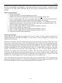
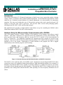
Application Note 141
Controlling a DS1804 Using an 8051Compatible Microcontroller
www.dalsemi.com
Introduction
The DS1804 Nonvolatile (NV) Trimmer Potentiometer is ideal for use in any system that requires a biasing
voltage, current, or resistance with or without manual adjustments. Its increment/decrement interface allows
either the use of minimal external hardware for manual adjustments or a microcontoller for autonomous
operation. The wiper can be adjusted to one of 100 positions, and any value can be stored in the part’s NV
register to select the wiper value at power-up. The part also offers several small packaging options,
including 8-pin DIP, SOIC, µSOP, and flip-chip packages.
This application note provides a simple hardware and software set-up for controlling the DS1804 with a
Dallas Semiconductor DS87C520 (8051) Microcontroller.
Hardware Setup for Microcontoller Communication with a DS1804
One of the primary benefits of using a DS1804 is the simplicity of the hardware and software control
interface. Only three connections are required between the potentiometer and the microcontroller: chip
select, up/down select, and increment, which are on pins P1.6, P1.5, and P1.4 of the microcontroller in
Figure 1, respectively. Two additional components for supporting the 8051 program are shown on the
schematic. The first is a DS1075 EconOscillator chip that provides a 22.22 MHz clock for the 8051; an LED
attached to P1.0 is the second. Functioning as a status indicator in the program, the LED is toggled
intermittently to show that the program is still executing.
Figure 1. Schematic Showing the DS87C520, DS1804, and DS1075 Connections
The DS1075 can be replaced with a 22.118 MHz crystal. Instructions for operating the DS87C520 with a
crystal clock source are available in Dallas Semiconductor’s High Speed Microcontroller User’s Manual. It
should be noted that the DS87C520 is capable of operating with up to a 33 MHz clock; however, the delays
used in the software depend upon the clock frequency. Operating the DS87C520 at a higher clock rate can
potentially cause timing faults with the DS1804, while operating at a lower frequency should have no ill
effects.
1 of 11
031201
AN 141
Using the CS, INC, and UD Signals to Control the DS1804
Operation of the DS1804 is simple, but a couple of nuances need to be understood for reliable operation.
First, the device powers up over the course of 50ms. Attempts to signal information to the part before that
period of time elapses will not be successful. The part also requires 500µs to adjust the value of the wiper to
the value stored in the non-volatile register during power-up.
After power-up, there are two ways to increment or decrement the part. The first method only changes the
value of the potentiometer wiper position. The second changes both the value of the wiper and writes the
current value to the non-volatile register.
Changing the wiper position without writing to the non-volatile register is accomplished by the following:
1.
2.
3.
4.
5.
6.
Adjust the up/down select input to high for increment or low for decrement.
Enable the chip by asserting the CS signal (active low).
Pulse INC low n-1 times to in/decrement the part n times.
Assert INC low again (the part in/decrements one more time on the falling edge of INC).
Disable the chip by de-asserting CS.
De-assert INC to complete the write.
To change the value of the wiper and write the final wiper position to the nonvolatile register, complete the
following sequence:
1.
2.
3.
4.
5.
Adjust the up/down select input to high for increment or low for decrement.
Enable the chip by asserting the CS signal (active low).
Pulse the increment signal low n times to in/decrement the part n positions.
Disable the chip by de-asserting CS.
Wait 10ms for present wiper position to be written to NV register.
Another simple, useful routine stores the current value of the wiper position into the NV register. Pulsing
CS low while increment remains high stores the current value of the wiper into the NV register. After CS is
de-asserted, the controller should wait for 10ms to elapse for the NV register to be written with the present
wiper position.
8051 Software for Controlling a DS1804
There are millions of different routines that could be used for adjusting the wiper position and writing to the
NV register of a DS1804; however, the easiest method requires only four routines. These routines initialize
the DS1804, increment the chip one wiper position, decrement the chip one wiper position, and write the
current wiper position to the NV register. These routines are provided in Appendix A, and are called
Init1804, Increment1804, Decrement1804, and WriteNVreg. The Increment1804 and Decrement1804
routines can be placed in a loop to in/decrement the DS1804 n times, and once the desired wiper location is
reached it can be written to the NV register by calling the WriteNVreg routine. If it is desirable to
in/decrement the DS1804 n times without writing the loop in the main program, a short routine could be
written that receives n from the stack or the accumulator and implements the loop’s function.
The downfall of using only four functions occurs when the overhead of selecting Up/Down and CS during
each adjustment slows operation down too much for the application at hand. Thus, two additional functions
are included that demonstrate in/decrementing the chip (five intervals each way) with a single selection both
the direction and chip select inputs. These routines are called Increment1804x5 and Decrement1804x5.
2 o f 11
AN 141
In addition to the routines described above, three other routines reside in the software to generate timing.
They are called wait16us, wt and wait3sec. These function provide a fixed 1.6µs delay, a variable delay that
is selected by the values stored in R5, R6, and R7, and a fixed 3-second delay that is used in the main
program.
Main Program Sequence
1. Disables all interrupts.
2. Toggles LED on P1.0 to signify beginning of execution.
3. Initializes the DS1804 by setting all three DS1804 inputs high and waiting 50ms.
4. Waits 3 seconds, toggles LED. The 3-second delay allows the power up value of the DS1804 to
be read with a multi-meter, and the LED indicates when changes are occurring.
5. Increments the DS1804 in 5 interval bursts, a total of 25 positions. A 3-second pause has been
added between each of the 5-interval bursts to allow a multi-meter to monitor the changes. The
LED will toggle as the changes to the wiper occur.
6. Waits 3 seconds, toggles the LED, and decrements the DS1804 5 intervals.
7. Writes the NV register to the current value.
8. Waits 3 seconds, toggles the LED, and increments the DS1804 1 interval.
9. Waits 3 seconds, toggles the LED, and decrements the DS1804 1 interval.
10. Completes execution with an infinite loop.
Main Program Output
Assume that you are executing the program with Vcc at 5V with a 22 MHz crystal; a multi-meter is
connected between W and Gnd; and cycling Vcc from Gnd to 5V starts the program. The output of the
DS1804 will be as follows.
When power is turned on, the part will boot up to the value last stored in the NV register. If the value of the
NV register was previously written, then it will display that value; otherwise it will display the pseudorandom value stored in the NV register by the factory before shipping. The wiper output will display the
voltage on the multi-meter that corresponds to the value stored in the NV register for 3 seconds. The output
will then incremented in 0.25V steps and hold each value for 3 seconds before moving on to then next
position. This will occur five times for a total voltage change of 1.25V. The wiper voltage will then be
lowered 0.25V, and that value will be held for 3 seconds. This value will be stored in the NV register and
will be the value that the part boots up to the next time power is cycled. Finally, the wiper voltage will be
incremented 0.05V and then decremented 0.05V, with both values being held for 3 seconds. The LED
attached to P1.0 will be toggled every 3 seconds directly before every change occurs.
In the event that the chip powers up with a wiper value equal to or greater than 3.76V, the program will
attempt to increment the chip past 5V. This does not damage the part, but the output will remain at 5V until
a decrement command is issued. Thus the end voltage in this case would be 4.75V.
3 o f 11
AN 141
Dallas Semiconductor Contact Information
Address:
4401 S. Beltwood Parkway
Dallas, TX 75244
Tel: 972-371-4448
Fax: 972-371-4799
World Wide Web Site:
www.dalsemi.com
Product Literature:
(972) 371-4448
FTP Site:
ftp://ftp.dalsemi.com
Sales and Customer Service:
(972) 371-4969
Datasheets:
www.dalsemi.com/datasheets/pdfindex.html
Ordering Information:
www.dalsemi.com/products/ordering.pdf
Package/Mechanical Drawings:
www.dalsemi.com/datasheets/mechdwg.html
4 o f 11
AN141
Appendix A – 8051 Software Used to Communicate with the DS1804
;*********************************************************************
;* DS87C520 APPS DEVELOMENT SYSTEM
*
;*
*
;* Application: Communication with a DS1804
*
;*********************************************************************
;*
*
;* Software Revision History
*
;*
*
;* 1.0 02/07/01 - First try at operating a DS1804 using the
*
;*
generic application engineering generic 8051
*
;*
boot loading board.
*
;*
*
;* Hardware Description
*
;*
*
;* P1.0 - LED
P0.0 - SN74F373N
*
;* P1.1 P0.1 "
*
;* P1.2 - RXD1 – Not used
P0.2 "
*
;* P1.3 - TXD1 – Not used
P0.3 "
*
;* P1.4 - nInc
P0.4 "
*
;* P1.5 - UnD
P0.5 "
*
;* P1.6 - nCS
P0.6 "
*
;* P1.7 P0.7 "
*
;*
*
;* P3.0 - RXD0 - Not used
P2.0 - Upper
*
;* P3.1 - TXD0 - Not used
P2.1 - Address
*
;* P3.2 P2.2 - Byte
*
;* P3.3 P2.3 - "
*
;* P3.4 P2.4 - "
*
;* P3.5 P2.5 - "
*
;* P3.6 - WR\
P2.6 - "
*
;* P3.7 - RD\
P2.7 - "
*
;*
*
;* Window 0 R0 - Used as scratch pad, destroy with caution!
*
;* Window 0 R5-R7 Used for timer/scratch pad, destroy with caution! *
;*********************************************************************
$include (c:\firmware\reg520.inc)
; SFR register defs for compiler
;************* Variable Declarations *************
;** General Variables **
stack
equ
02Fh
; bottom of stack
; stack starts at 30h
;*************
SFR Declarations
*************
;** General SFR Names **
smod_1
equ
0DFh
; buad rate doubler bit declared
5 o f 11
AN141
;** Port 1 Signal Names **
LED
equ
90h
RX1
TX1
nInc
UnD
nCS
equ
equ
equ
equ
equ
92h
93h
94h
95h
96h
;
;
;
;
;
;
;
;
P1.0
P1.1
P1.2
P1.3
P1.4
P1.5
P1.6
P1.7
is
is
is
is
is
is
is
is
LED
not used
Serial Port 1 RX
Serial Port 1 TX
not Inc, - 1804
Up not Down - 1804
not ChipSelect - 1804
not used
;*********************************************************************
;* Hardware Interrupt Vectors (Table on page 95 of DS databook)
*
;*********************************************************************
;* No Interrupts are enabled in this code. If interrupts are to be *
;*
enabled they need to have the label initialized here.
*
;*********************************************************************
org
0000h
; Power up and Reset
ljmp
start
org
0003h
; External Interrupt 0
ljmp
start
org
000Bh
; Timer 0 Interrupt
ljmp
start
org
0013h
; External Interrupt 1
ljmp
start
org
001Bh
; Timer 1 Interrupt
ljmp
start
org
0023h
; Serial Port 0 Interrupt
ljmp
start
org
002Bh
; Timer 2 Interrupt
ljmp
start
org
0033h
; PowerFail Interrupt (DS Priority 1)
ljmp
start
org
003Bh
; Serial Port 1 Interrupt (DALLAS)
ljmp
start
org
0043h
; External Interrupt 2 (DALLAS)
ljmp
start
org
004Bh
; External Interrupt 3 (DALLAS)
ljmp
start
org
0053h
; External Interrupt 4 (DALLAS)
ljmp
start
org
005Bh
; External Interrupt 5 (DALLAS)
ljmp
start
org
0063h
; Watchdog Interrupt (DALLAS)
ljmp
start
org
006Bh
; Real-Time Clock (DALLAS)
ljmp
start
6 o f 11
AN141
;*********************************************************************
;**** The Main Program demonstrates using a 8051 to communicate ****
;**** with a DS1804. The program increments and decrements the ****
;**** potentiometer without writing the NV Register, and it
****
;**** demonstrates writing to the NV Register as well.
****
;*********************************************************************
org
0080h
; location that hardware begins execution
start:
;
after a reset.
clr
EA
; Disable Interrupts
cpl
LED
; Complement LED - Identifies that the
;
program has started execution
lcall init1804
; initializes DS1804, must be done in first
;
50ms to avoid the three inputs becoming
;
active without them being in a known
;
state.
lcall wait3sec
; give time to read the last NVReg value
; on a multimeter
cpl
LED
; toggle LED
mov
R0, #5
; increment the 1804 by 5 intervals, 5 times,
loop10:
;
with 3 seconds between increments
lcall Increment1804x5 ; increment the DS1804
lcall wait3sec
; waits 3 seconds
cpl
LED
; toggle LED
djnz R0, loop10
lcall Decrement1804x5 ; decrement the 1804 5 intervals
cpl
LED
; toggle LED
lcall WriteNVreg
; write current value to NVReg. Now 20 steps
;
greater that the start of execution.
lcall wait3sec
; wait 3 seconds for multimeter use
cpl
LED
; complement LED
lcall Increment1804
; increment 1804 once, don't write NVReg
lcall wait3sec
; wait 3 seconds for multimeter use
cpl
LED
; Complement LED
lcall Decrement1804
; decrement 1804 once, don't write NVReg
lcall wait3sec
; wait 3 seconds for multimeter use
cpl
LED
; Complement LED
EndOfMain:
; wait forever
sjmp EndOfMain
7 o f 11
AN141
;*********************************************************************
;****
Increment DS1804x5 Routine
****
;****
Increments the chip 5 times without de-selecting the
****
;****
the chip between increments. This does not write to the ****
;****
nonvolatile register.
****
;*********************************************************************
;*
Uses no other routines, and destroys no registers
*
;*********************************************************************
Increment1804x5:
setb UnD
; select increment
clr
nCS
; select chip
clr
nInc
; clear inc - increase to next position
setb nInc
; set nInc back to inactive state.
clr
nInc
; clear inc - increase to next position
setb nInc
; set nInc back to inactive state.
clr
nInc
; clear inc - increase to next position
setb nInc
; set nInc back to inactive state.
clr
nInc
; clear inc - increase to next position
setb nInc
; set nInc back to inactive state.
clr
nInc
; clear inc - increase to next position
setb nCS
; set nCS before nInc to avoid writing to
;
the NV EEPROM register in the DS1804
setb nInc
; set nInc back to inactive state.
ret
;*********************************************************************
;****
Increment DS1804 Routine
****
;****
Increments the chip 1 time, and de-selects the chip
****
;****
without writing to the nonvolatile register.
****
;*********************************************************************
;*
Uses no other routines, and destroys no registers
*
;*********************************************************************
Increment1804:
setb UnD
; select increment
clr
nCS
; select chip
clr
nInc
; clear inc - increase to next position
setb nCS
; set nCS before nInc to avoid writing to
;
the NV EEPROM register in the DS1804
setb nInc
; set nInc back to inactive state.
ret
8 o f 11
AN141
;*********************************************************************
;****
Decrement DS1804x5 Routine
****
;****
Decrements the chip 5 times without de-selecting the
****
;****
the chip between decrements. This does not write to the ****
;****
nonvolatile register.
****
;*********************************************************************
;*
Uses no other routines, and destroys no registers
*
;*********************************************************************
Decrement1804x5:
clr
UnD
; select increment
clr
nCS
; select chip
clr
nInc
; clear inc - increase to next position
setb nInc
; set nInc back to inactive state.
clr
nInc
; clear inc - increase to next position
setb nInc
; set nInc back to inactive state.
clr
nInc
; clear inc - increase to next position
setb nInc
; set nInc back to inactive state.
clr
nInc
; clear inc - increase to next position
setb nInc
; set nInc back to inactive state.
clr
nInc
; clear inc - increase to next position
setb nCS
; set nCS before nInc to avoid writing to
;
the NV EEPROM register in the DS1804
setb nInc
; set nInc back to inactive state.
ret
;*********************************************************************
;****
Decrement DS1804 Routine
****
;****
Decrements the chip 1 time, and de-selects the chip
****
;****
without writing to the nonvolatile register.
****
;*********************************************************************
;*
Uses no other routines, and destroys no registers
*
;*********************************************************************
Decrement1804:
clr
UnD
; select decrement
clr
nCS
; select chip
clr
nInc
; clear inc - decrease to next position
setb nCS
; set nCS before nInc to avoid writing to
;
the NV EEPROM register in the DS1804
setb nInc
; set nInc back to inactive state.
ret
9 o f 11
AN141
;*********************************************************************
;****
DS1804 Write Nonvolatile Register Routine
****
;****
Writes the Nonvolatile Register to the current wiper
****
;****
value, and then waits 10ms for the write to occur.
****
;*********************************************************************
;*
Uses wt routine, and destroys registers R5, R6, and R7
*
;*********************************************************************
WriteNVreg:
clr
nCS
; select chip
setb nCS
; deselect chip, nInc already high so the
;
DS1804 will store to the NV Register
mov
R5, #255
; wait 10ms before continuing, the NV Reg.
mov
R6, #3
; storage time
mov
R7, #1
;
lcall wt
;
ret
;*********************************************************************
;****
Initialize DS1804 Routine
****
;****
Sets all three control signals to their inactive state, ****
;****
and waits 50ms for the inputs to become active before
****
;****
returning to the main program.
****
;*********************************************************************
;*
Uses wt routine, and destroys registers R5, R6, and R7
*
;*********************************************************************
init1804:
setb nCS
; de-select 1804
setb nInc
; de-activate Increment Signal
setb UnD
; select increment
mov
mov
mov
lcall
ret
R5, #255
R6, #15
R7, #1
wt
; wait 50ms, this is done so communication
;
will not begin before the DS1804 is ready
;
to accept input.
;
;*********************************************************************
;****
Wait 3 Seconds Function
****
;*********************************************************************
;*
requires wt routine, and destroys R5, R6 and R7
*
;*********************************************************************
wait3sec:
mov
R5, #255
; wait 3 sec., this is done so advances can
mov
R6, #147
;
be watched on a multi-meter
mov
R7, #6
;
lcall wt
;
ret
10 o f 11
AN141
;*********************************************************************
;****
General Wait Function
****
;****
Can wait anywhere between 14.42us to 221 sec.
****
;****
Waits R7 * 867.6 ms if R5 = R6 = 255
****
;****
Waits R6 * 3.4 ms
if R5 = 255 and R7 = 1
****
;****
Waits R5 * 13.34us if R6 = R7 = 1
****
;*********************************************************************
;*
requires wait16us routine
*
;*
destroys R5, R6, and R7 registers
*
;*********************************************************************
wt:
lcall wait16us
; 12.8us of waits
lcall wait16us
lcall wait16us
lcall wait16us
lcall wait16us
lcall wait16us
lcall wait16us
lcall wait16us
djnz R5, wt
;Wait = R5 * 13.34us + 1.1us if R6 = R7 = 1
djnz R6, wt
;Wait = R6 * 3.4ms
if R5 = 255, R7 = 1
djnz R7, wt
;Wait = R7 * 867.6ms
if R5 = R6 = 255
ret
;*********************************************************************
;****
Wait 1.6 us Function
****
;****
Wastes 1.6us of processor time with call, nop and return ****
;*********************************************************************
;*
Requires no other routines or registers
*
;*********************************************************************
wait16us:
nop
; 1 nops @4cc each + lcall @16cc + ret @16cc
; produces approximately 1.6us of delay with a
; 22.22MHz clock
ret
END
;End of program
11 o f 11