1
a
Silicon Anomaly List
TigerSHARC®
Embedded Processor
ADSP-TS201S
ABOUT ADSP-TS201S SILICON ANOMALIES
These anomalies represent the currently known differences between revisions of the TigerSHARC ADSP-TS201S product(s) and the
functionality specified in the ADSP-TS201S data sheet(s) and the Hardware Reference book(s).
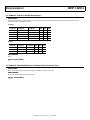
SILICON REVISIONS
A silicon revision number with the form "-x.x" is branded on all parts (see the data sheet for information on reading part branding). The
silicon revision can also be electronically read by reading the IDCODE register either via JTAG or DSP code.
The following DSP code can be used to read the register:
<UREG> = IDCODE;;
Silicon REVISION
IDCODE[31:28]
2.0
0100
1.2
0011
1.1
0010
ANOMALY LIST REVISION HISTORY
The following revision history lists the anomaly list revisions and major changes for each anomaly list revision.
Date
Anomaly List Revision
Applicable Data Sheet Revision
Additions and Changes
01/08/2008
Q
C
Added anomalies: 03000376
09/25/2007
P
C
Added anomalies: 03000375
08/08/2007
O
C
Modified anomalies: 03000373
05/23/2007
N
C
Added anomalies: 03000372, 03000373
09/22/2006
M
B
Added anomalies: 03000371
08/01/2006
L
B
Added anomalies: 03000360, 03000364, 03000367,
03000368
Modified anomalies: 03000357
01/21/2006
K
A
Added anomalies: 03000358, 03000359
10/27/2005
J
A
Added anomalies: 03000357
10/03/2005
I
A
Added anomalies: 03000348, 03000349, 03000350,
03000351, 03000352, 03000353
NR002910Q
Information furnished by Analog Devices is believed to be accurate and reliable.
However, no responsibility is assumed by Analog Devices for its use, nor for any
infringements of patents or other rights of third parties that may result from its use.
Specifications subject to change without notice. No license is granted by implication or
otherwise under any patent or patent rights of Analog Devices. Trademarks and
registered trademarks are the property of their respective owners.
One Technology Way, P.O.Box 9106, Norwood, MA 02062-9106 U.S.A.
Tel: 781.329.4700
www.analog.com
Fax: 781.461.3113
©2008 Analog Devices, Inc. All rights reserved.
ADSP-TS201S
Silicon Anomaly List
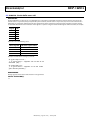
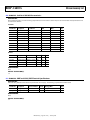
SUMMARY OF SILICON ANOMALIES
The following table provides a summary of ADSP-TS201S anomalies and the applicable silicon revision(s) for each anomaly.
No.
ID
Description
1.1
1.2
2.0
1
03000168
First instruction of an ISR has to be quad-aligned
x
x
x
2
3
03000192
Protection does not prevent writes
x
x
x
03000206
RTI or RETI instruction followed by CJMP relative
x
x
x
4
03000208
Link read status after read Rx register
x
x
x
5
03000211
BTB on jump from internal to external address
x
x
x
6
03000214
Trace buffer samples the wrong PC at WP1 exception
x
x
x
7
03000216
SQSTAT update and read
x
.
.
8
03000220
Read of link status after error in a write to a link control
x
x
x
9
03000236
External Port DMA chaining may fail when paused
x
x
x
10
03000263
FLYBY On 64 Bit Bus Supports Long Transactions Only
x
x
x
11
03000296
Predicted jump from external to internal updates the BTB
x
x
.
12
03000297
Write to SFREG in the same line with conditional jump may fail
x
.
.
13
03000298
Missed stall on ACS/MAX/TMAX after conditional ACS/MAX/TMAX
x
x
.
14
03000299
Missed stall on conditional circular buffer store
x
.
.
15
03000300
Link Transmits Port Enable Timing Restrictions
x
x
.
16
03000302
Reading from SDRAM when SDREN bit in SDRCON is clear causes deadlock
x
x
x
17
03000304
Interrupt routine for the same interrupt is serviced every time we reach idle with HW interrupt
enable bit clear
x
x
x
18
03000305
Instructions not executed correctly upon Entering emulation space
x
.
.
19
03000306
PC of interrupt during idle is corrupted due to stall
x
x
x
20
03000307
Missing stall on ISF use
x
.
.
21
03000315
Aborted conditional memory access may cause an exception
x
x
.
22
03000316
Do not use IALU or Sequencer instructions in the first quad of an ISR
x
x
x
23
03000317
Erroneous BTB update
x
.
.
24
03000319
Missing exception on illegal read from external memory to sequencer/debug registers
x
x
.
25
03000320
Circular buffer stores stall
x
.
.
26
03000321
Link Port LVDS Electrical Characteristics
x
.
.
27
03000323
Condition flag not updated after sum/abs instruction is followed by an aborted ALU instruction
x
x
.
28
03000324
Link Port LVDS AC Characteristics
x
.
.
29
03000326
External DAB Results in Erroneous Results in Certain Cases
x
x
.
30
03000327
Duty Cycle Requirement for Low Frequency SCLK
x
.
.
31
03000328
Conditional E2 instructions that are aborted still generate exceptions
x
x
.
32
03000329
Some exceptions are missed when they follow a not-acknowledged transaction
x
x
.
33
03000330
Link Port Transmit Rise / Fall Times Violate Spec
x
x
x
34
03000331
Weakest Drive Strength Setting is Not Functional
x
x
x
35
03000332
EXCAUSE is not updated when watchpoint exception occurs and emulation is enabled
x
x
.
36
03000333
Single-step software exception is not generated when return from the exception routine is a BTB
hit
x
x
x
37
03000337
Link Port LVDS internal differential resistors
x
.
.
38
03000339
Locking cache may cause memory access failures
x
x
.
39
03000341
Link Port LVDS Electrical Characteristics
.
x
.
40
03000342
Link Port LVDS AC Characteristics
.
x
.
NR002910Q | Page 2 of 29 | January 2008
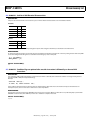
ADSP-TS201S
Silicon Anomaly List
No.
ID
Description
1.1
41
03000346
VREF and SCLK_VREF Electrical Specifications
x
.
.
42
03000347
Do not update global static flags in the same line with write SQ / BD registers
x
x
x
43
03000348
Extra writes to AutoDMA may cause cluster bus deadlock
x
x
x
44
03000349
Emulation mode allows multiple writes to SYSCON and SDRCON
x
x
x
45
03000350
FLOAT BY instruction with truncate (T) option generates wrong result
x
x
x
46
03000351
Subtract with divide by two instruction with signed round to nearest even option generates
wrong result
x
x
x
47
03000352
Link Transmits Port Enable Timing Restrictions
.
.
x
48
03000353
Conditional E2 instructions that are aborted still update EXCAUSE
.
.
x
49
03000357
Link Port LVDS Electrical Characteristics
.
.
x
50
03000358
Initial load MR register instruction can fail
.
.
x
51
03000359
Compute block source register busses can fail to initialize properly
.
.
x
52
03000360
Predicated RETIB load (store) instructions fail
x
x
x
53
03000364
AC Signal Specifications - Input Hold
x
x
.
54
03000367
Link Port Transmit 4-bit mode enable failure
.
.
x
55
03000368
Link port receive enable after disable failure
x
x
x
56
03000371
SCLK_Vref Specification
.
x
x
57
03000372
TIMER enable/disable restriction
x
x
x
58
03000373
PLL Failure to Lock at Power-Up
x
x
x
59
03000375
DMA for link port to/from external memory may be blocked
x
x
x
60
03000376
Link port receive to link port transmit DMA fails
x
x
.
Key: x = anomaly exists in revision
. = Not applicable
NR002910Q | Page 3 of 29 | January 2008
1.2
2.0
ADSP-TS201S
Silicon Anomaly List
DETAILED LIST OF SILICON ANOMALIES
The following list details all known silicon anomalies for the ADSP-TS201S including a description, workaround, and identification of
applicable silicon revisions.
1. 03000168 - First instruction of an ISR has to be quad-aligned:
DESCRIPTION:
If the first instruction of an interrupt service routine is not quad-aligned, the sequencer may fail to execute properly.
WORKAROUND:
Quad-align all ISRs with .align_code 4; directive. Note that if the ISR is in a separate module, the linker will quad-align it
automatically.
APPLIES TO REVISION(S):
1.1, 1.2, 2.0
2. 03000192 - Protection does not prevent writes:
DESCRIPTION:
When writing to the protected registers (i.e. all registers except the compute block and the IALU) in USER mode, the transaction is
executed and the data is written to the target register. The exception, if enabled, is still generated.
WORKAROUND:
None.
APPLIES TO REVISION(S):
1.1, 1.2, 2.0
3. 03000206 - RTI or RETI instruction followed by CJMP relative:
DESCRIPTION:
Relative CJMP and CJMP_CALL branch instructions can branch to an unpredictable target.
WORKAROUND:
All CJMP and CJMP_CALL branch instructions must be used with option (ABS).
APPLIES TO REVISION(S):
1.1, 1.2, 2.0
NR002910Q | Page 4 of 29 | January 2008
ADSP-TS201S
Silicon Anomaly List
4. 03000208 - Link read status after read Rx register:
DESCRIPTION:
If data is read from link receive buffer, and immediately on the next cycle the status register is read, it may still contain the old (before the
buffer read) value.
WORKAROUND:
The LRSTATx register should always be read twice sequentially as follows:
XR0 = LRSTATx;;
XR1 = LRSTATx;;
The second read will ensure the contents of the status register have been updated. If a destructive read is desired, the sequence should
be as follows:
XR0 = LRSTATx;;
XR1 = LRSTATx;;
XR2 = LRSTATCx;;
APPLIES TO REVISION(S):
1.1, 1.2, 2.0
5. 03000211 - BTB on jump from internal to external address:
DESCRIPTION:
In case of jump from internal address to external address with prediction "taken", the entry is written into the BTB, but with valid bit
cleared. This causes a useless replacement in BTB since the new entry has LRU value cleared (i.e. invalid).
WORKAROUND:
This is a minor performance issue. When it is known that branching is to external memory, use of (NP) option will prevent a useless BTB
entry.
APPLIES TO REVISION(S):
1.1, 1.2, 2.0
6. 03000214 - Trace buffer samples the wrong PC at WP1 exception:
DESCRIPTION:
In case of WP1 exception, the TRCB samples the next instruction address after the instruction that caused the exception.
Example:
The WP1 generates exception on transaction on JALU access (line 0x00080025). The TRCB will sample the next address (0x00080026).
After the exception (RTI) the TRCB will sample this address again.
TRCB0
TRCB1
TRCB2
TRCB3
0x00080026
0x00010000 - Exception routine address
0x00010010 - RTI
0x00080026
WORKAROUND:
None
APPLIES TO REVISION(S):
1.1, 1.2, 2.0
NR002910Q | Page 5 of 29 | January 2008
ADSP-TS201S
Silicon Anomaly List
7. 03000216 - SQSTAT update and read:
DESCRIPTION:
Reading the SQSTAT immediately after it is updated gives the old value.
WORKAROUND:
Read SQSTAT twice sequentially, as follows:
XR0 = SQSTAT;;
XR1 = SQSTAT;;
The second read of SQSTAT will ensure that SQSTAT has been updated. Note that bits SQSTAT[22:20], which are Global Interrupt Disable,
Exception Active and Emulation active are possibly modified by RTI, thus these bits cannot be read reliably in any interruptible code.
APPLIES TO REVISION(S):
1.1
8. 03000220 - Read of link status after error in a write to a link control:
DESCRIPTION:
If data written to one of the link control registers (LTCTL or LRCTL) causes an error condition, and on the next cycle of the SOC bus the
corresponding status register (LTSTAT or LRSTAT) is read, the read access might not show that error.
WORKAROUND:
Execute a dummy read on the SOC bus first, for example:
LTCTL = <Ureg>;;
<Ureg> = LTSTATx;;
<Ureg> = LTSTATx;;
/* this is a dummy read to be ignored */
/* this is the real read to be used */
APPLIES TO REVISION(S):
1.1, 1.2, 2.0
9. 03000236 - External Port DMA chaining may fail when paused:
DESCRIPTION:
If an external port DMA is paused during chaining when one of the two TCB's has chained while the other has not, and then TCBs are
modified, un-pausing the DMA will result in a chaining failure and the DMA channel will be stuck.
WORKAROUND:
If such a DMA process is required (as it may be in cases of chain insertions), after pausing the type field of the two DP registers must be
examined. If both are legal or both are inactive (000), continue with the modification of the TCB's as required. Otherwise (which is the case
when one has chained and the other has not), un-pause the channel, wait, pause and check again.
APPLIES TO REVISION(S):
1.1, 1.2, 2.0
NR002910Q | Page 6 of 29 | January 2008
ADSP-TS201S
Silicon Anomaly List
10. 03000263 - FLYBY On 64 Bit Bus Supports Long Transactions Only:
DESCRIPTION:
FLYBY transactions must be long transactions when in the 64 bit external bus mode.
WORKAROUND:
When the external memory is set to 64 bit bus, a FLYBY DMA TCB must be set to long word transactions.
APPLIES TO REVISION(S):
1.1, 1.2, 2.0
11. 03000296 - Predicted jump from external to internal updates the BTB:
DESCRIPTION:
Predicted branch from external memory space to internal memory space when the BTB is enabled may fail.
WORKAROUND:
All branches in code in external memory should be (NP).
APPLIES TO REVISION(S):
1.1, 1.2
12. 03000297 - Write to SFREG in the same line with conditional jump may fail:
DESCRIPTION:
In the following instruction:
if cond, jump...; sfreg = [mem]/UREG;;
SFREG register may not get the new value if the condition of the jump is any condition other than an IALU or a loop counter condition.
WORKAROUND:
Do not write to SFREG in the same instruction line that has a jump based on a condition other than an IALU or a loop counter condition.
Note that the problematic sequence includes condition TRUE, i.e. unconditional branches.
APPLIES TO REVISION(S):
1.1
NR002910Q | Page 7 of 29 | January 2008
ADSP-TS201S
Silicon Anomaly List
13. 03000298 - Missed stall on ACS/MAX/TMAX after conditional ACS/MAX/TMAX:
DESCRIPTION:
If a conditional ACS, MAX or TMAX (T/MAX) or TR load is, within the next two cycles, followed by an ACS or T/MAX instruction line, the last
instruction may give wrong results. For example,
a. (1) if <cond>; do, sTR1 = T/MAX();;
(2) inst ;;
(3) sTR2 = ACS( TR1, ...) ;;
b. (1) if <cond>; do, TR1 = T/MAX();;
(2) TR2 = ACS (TR1, ...);;
WORKAROUND:
Either of the following:
1. Use T/MAX instruction unconditionally.
2. After a conditional T/MAX instruction, add two lines of NOP;;.
APPLIES TO REVISION(S):
1.1, 1.2
14. 03000299 - Missed stall on conditional circular buffer store:
DESCRIPTION:
When a conditional (condition other than IALU or loop counter) circular-buffer store to memory which updates J/Km by post-modify is
followed by an IALU instruction with a dependency on the same J/Km, there should be a 4-cycle stall. This stall is not implemented.
For example, the following sequence
(1) if cond; do, CB [j0+=4]=xr0;;
(2) j1=j0+j2;;
can result in a wrong value used for J0 in the second instruction.
WORKAROUND:
There are two suggested workarounds, either one can be used.
(1) Avoid using circular buffer store on conditions other than IALU and loop counter.
(2) Maintain no less than four instruction lines between the problematic conditional circular buffer store and the corresponding IALU
register use, by inserting NOP;; lines if necessary.
APPLIES TO REVISION(S):
1.1
NR002910Q | Page 8 of 29 | January 2008
ADSP-TS201S
Silicon Anomaly List
15. 03000300 - Link Transmits Port Enable Timing Restrictions:
DESCRIPTION:
TVACANT of the LTSTATx register does not correctly indicate the DLL lock state. A software delay is required between enabling the link
transmit port and initializing the corresponding DMA or polling routine responsible for driving the transmit data. The minimum required
delay is (75000 x TL) where TL is the period of the corresponding LxCLKO.
Also, when disabling and reenabling a link transmit port, a delay of at least 100 ns is required after the disable and before the reenable.
WORKAROUND:
1. Implement the required delay in software, from enabling of a link transmit port to initialization of the corresponding TCB or polling
routine.
2. Implement a 100ns delay in software, from disabling of a link transmit port to reenabling of the same port.
APPLIES TO REVISION(S):
1.1, 1.2
16. 03000302 - Reading from SDRAM when SDREN bit in SDRCON is clear causes deadlock:
DESCRIPTION:
Reading SDRAM when SDREN bit in SDRCON register is clear will cause deadlock.
WORKAROUND:
Ensure that SDRAM is enabled in SDRCON before accessing it.
APPLIES TO REVISION(S):
1.1, 1.2, 2.0
17. 03000304 - Interrupt routine for the same interrupt is serviced every time we reach idle with HW
interrupt enable bit clear:
DESCRIPTION:
If the processor is at idle, global interrupts enable bit SQCTL[2] is cleared and an interrupt arrives, sequencer operation may become
unpredictable.
WORKAROUND:
Always enable global interrupts SQCTL[2] before idle - this is normal operation even without the anomaly.
APPLIES TO REVISION(S):
1.1, 1.2, 2.0
18. 03000305 - Instructions not executed correctly upon Entering emulation space:
DESCRIPTION:
If the processor is asynchronously halted (Debug -> Halt or Debug -> Multiprocessor -> Halt from the emulator software) and then started
again (for example, Debug -> Run) by the emulator, the instruction at which it was halted may get executed twice.
WORKAROUND:
Do not asynchronously halt the processor by an emulator. Halting by breakpoints, watchpoints, stepping or running to cursor causes no
problems.
APPLIES TO REVISION(S):
1.1
NR002910Q | Page 9 of 29 | January 2008
ADSP-TS201S
Silicon Anomaly List
19. 03000306 - PC of interrupt during idle is corrupted due to stall:
DESCRIPTION:
If an instruction that generates a transaction to the OFIFO occurs within 3 or less core clock cycles prior to an IDLE instruction, the code
execution following an interrupt which breaks the processor out of IDLE may become unpredictable.
WORKAROUND:
Add 3 NOP;; lines before the Idle:
nop;;
nop;;
nop;;
Idle;;
and ensure that there are no branches to these NOP;; and IDLE;; instruction lines.
Also, to take care of possible returns from interrupts, ensure that either:
1. Last 3 instruction lines of an ISR contain no OFIFO accesses (i.e. no accesses to SOC or external memory).
OR
2. All RTI and RETI instructions have option (NP). Thus, in case an interrupt occurs during these NOPs, the return from that interrupt
will have a pipeline flush that will insert the required number of STALL cycles before the IDLE.
APPLIES TO REVISION(S):
1.1, 1.2, 2.0
20. 03000307 - Missing stall on ISF use:
DESCRIPTION:
The following sequence requires a 5-cycle stall that is not automatically inserted by the processor
(1) ISF0/1 =/+= cond ;; //all conditions other than IALU and loop counter
(2) ISF0/1 =/+= ISF0/1 ;;
(provided that it is the same GSFx register in destination of line 1 and source of line 2).
WORKAROUND:
Separate the two problematic instruction lines by at least 5 instruction lines (inserting NOPs, if necessary). For cases of branches to the
instruction flow that contains ISF0/1 =/+= ISF0/1, ensure that either
1. 4 instruction lines preceding the branch do not contain instruction ISF0/1 =/+= ISF0/1.
OR
2. The branch has (NP) option, thus inserting the necessary stall cycles.
APPLIES TO REVISION(S):
1.1
NR002910Q | Page 10 of 29 | January 2008
ADSP-TS201S
Silicon Anomaly List
21. 03000315 - Aborted conditional memory access may cause an exception:
DESCRIPTION:
The following instruction
if
or
if
or
if
or
if
<cond>; do UREG = Q[J/Kx + ...];;
<cond>; do UREG = Q[J/Kx += ...];;
<cond>; do UREG = L[J/Kx + ...];;
<cond>; do UREG = L[J/Kx += ...];;
may cause a misaligned or illegal access software exception if the condition is false. The exception can happen even if this aborted access
would have been aligned if the condition passed.
WORKAROUND:
1. Disable software exceptions.
2. Recognize a misaligned access or illegal address exception in the software exception handler and exit the handler.
APPLIES TO REVISION(S):
1.1, 1.2
22. 03000316 - Do not use IALU or Sequencer instructions in the first quad of an ISR:
DESCRIPTION:
An IALU or a sequencer instruction in the first quad word of an interrupt service routine may cause unpredictable results.
WORKAROUND:
Do not use IALU or Sequencer instructions in the first quad of an ISR.
APPLIES TO REVISION(S):
1.1, 1.2, 2.0
23. 03000317 - Erroneous BTB update:
DESCRIPTION:
On rare occasions BTB can get an entry with an erroneous tag. This can cause unpredictable code execution.
WORKAROUND:
Disable the BTB.
APPLIES TO REVISION(S):
1.1
NR002910Q | Page 11 of 29 | January 2008
ADSP-TS201S
Silicon Anomaly List
24. 03000319 - Missing exception on illegal read from external memory to sequencer/debug registers:
DESCRIPTION:
A read from external memory to sequencer (CJMP, RETI, RETIB, RETS, DBGE, LC0, LC1, SQCTL) or debug (WPxCTL, WPxL, WPxH, CCNTx,
PRFM, EMUCTL, EMUDAT, EMUIR) registers is illegal and should generate an exception. No exception is generated. In case of the
sequencer register, EXCAUSE field of SQSTAT is updated with the correct value of 0x7, but in case of the debug register, there is no
indication of the illegal access at all.
WORKAROUND:
When loading sequencer or debug registers from external memory, load the external memory data into a UREG first, then move the data
from UREG to the actual destination register.
APPLIES TO REVISION(S):
1.1, 1.2
NR002910Q | Page 12 of 29 | January 2008
ADSP-TS201S
Silicon Anomaly List
25. 03000320 - Circular buffer stores stall:
DESCRIPTION:
Circular buffer write can generate a 5 cycle dependency to a subsequent circular buffer use (thus, if the write and use are back-to-back,
this will result in a 5 cycle stall, if they are separated by one instruction, this will result in a 4 cycle stall, etc.) The occurence of the stalls is
dependent on a relationship between the two least significant bits of the registers that are being written of the first instruction and the
circular buffer IALU of the second instruction. If the register is a quad or a long, the lowest number register defines these bits, for example:
Register
LSBs
xR5
01
R7:6
10
yR15:12
00
J3:2
10
R7
11
The stalls occur in the following cases:
Addressing IALU
LSBs of the register written
J0/K0
00
J1/K1
01
J2/K2
10
J3/K3
11
Examples of combinations causing 5 cycle stalls:
cb Q[J1+=J2]=r17:16;;
// 5 cycle stall - register r16 to use of J0
J3=J0+J3 (CB);;
cb L[k2+=k31]=r7;;
// 5 cycle stall - register r7 to use of K3
yr21:20=cb L[k3+=k0];;
WORKAROUND:
Change registers used to ensure that the stalls are not generated.
APPLIES TO REVISION(S):
1.1
NR002910Q | Page 13 of 29 | January 2008
ADSP-TS201S
Silicon Anomaly List
26. 03000321 - Link Port LVDS Electrical Characteristics:
DESCRIPTION:
Link ports do not meet electrical characteristics specs. Link Port Electrical Characteristics are anomalized as follows:
Transmit:
Parameter
Min
Voh
Max
1.85V
Vol
0.92V
Vod
0.25V
0.65V
Vocm
1.20V
1.50V
Parameter
Min
Max
Vid
0.24V
0.70V
Vicm
1.00V
1.57V
Receive:
The anomalized specs are achieved by setting the link port drive strength to maximum, as described in the workaround.
WORKAROUND:
To enable link port functionality, all link ports must use maximum transmit drive strength. This is done by setting the test mode strap TM2
to low and adding the following lines to code before transmitting any data on link ports:
j0 = j31+0xFF01;;
TEST_MODES = j0;;
APPLIES TO REVISION(S):
1.1
27. 03000323 - Condition flag not updated after sum/abs instruction is followed by an aborted ALU
instruction:
DESCRIPTION:
If an instruction SUM or ABS is followed by an ALU instruction which is aborted (due to the failed condition or change in flow), the first
instruction (SUM or ABS) will not update the flags.
Example:
xr26=sum Br21(U);;
if xmle; do, xFr21:20=extd
r25;;
If the condition xmle fails, the first instruction will not update the flags. Note that the second instruction may be aborted due to an
interrupt and, thus, does not have to be conditional to cause the problem.
WORKAROUND:
Separate the second instruction from SUM/ABS instruction by one instruction. Make sure that there is no predicted jump in parallel with
SUM/ABS instruction that, with a BTB hit, branches to a conditional compute instruction.
APPLIES TO REVISION(S):
1.1, 1.2
NR002910Q | Page 14 of 29 | January 2008
ADSP-TS201S
Silicon Anomaly List
28. 03000324 - Link Port LVDS AC Characteristics:
DESCRIPTION:
The maximum frequency, minimum frequency, and several timing requirements and characteristics of the link ports do not meet
specification and are restricted as follows:
Transmit:
Parameter
Description
Conditions
Min
Max
Unit
tLCLKOP
LxCLKOUT Period
tLDOS
LxDATO Setup
tLCLKOP >= 8.0ns
4.0
1.1
12.5
ns
ns
tLDOS
LxDATO Setup
tLCLKOP < 8.0ns
0.6
ns
tLDOH
LxDATO Hold
tLCLKOP >= 8.0ns
1.1
ns
tLDOH
LxDATO Hold
tLCLKOP < 8.0ns
0.6
ns
Receive:
Parameter
Description
tLCLKIP
Conditions
Min
Max
Unit
LxCLKIN Period
4.0
20.0
ns
tLDIS
LxDATI Setup
0.5
ns
tLDIH
LxDATI Hold
0.5
ns
WORKAROUND:
None
APPLIES TO REVISION(S):
1.1
29. 03000326 - External DAB Results in Erroneous Results in Certain Cases:
DESCRIPTION:
Read accesses of external memory that use DABs or SDABs may return wrong data.
WORKAROUND:
Do not use external DAB and SDAB read accesses.
APPLIES TO REVISION(S):
1.1, 1.2
NR002910Q | Page 15 of 29 | January 2008
ADSP-TS201S
Silicon Anomaly List
30. 03000327 - Duty Cycle Requirement for Low Frequency SCLK:
DESCRIPTION:
For lower frequency SCLK, a tighter duty cycle is required than specified in the data sheet. The anomalized requirement is as follows:
Parameter
Description
Condition
Min
Max
Unit
tSCLKH
System Clock Cycle High Time
tSCLK>=13.33ns
0.45*tSCLK
0.55*tSCLK
ns
tSCLKL
System Clock Cycle Low Time
tSCLK>=13.33ns
0.45*tSCLK
0.55*tSCLK
ns
Operation of the chip at SCLK frequency lower than 40 MHz is not supported.
WORKAROUND:
SCLK frequency must be 40 MHz or higher. For SCLK frequency of 40-75 MHz ensure max duty cycle of 55/45.
APPLIES TO REVISION(S):
1.1
31. 03000328 - Conditional E2 instructions that are aborted still generate exceptions:
DESCRIPTION:
Some illegal instructions that are conditional on CONDE2 (compute block condition) may generate an exception, even if the condition
was evaluated as false and the instruction was aborted.
The problem occurs for the following illegal instructions:
1. Two external loads to the same quad register in the same instruction line.
2. Misaligned access by the IALU.
3. Illegal address access by the ILAU.
WORKAROUND:
Ensure that all conditional instructions are legal, even if the condition is expected to evalute as false.
APPLIES TO REVISION(S):
1.1, 1.2
32. 03000329 - Some exceptions are missed when they follow a not-acknowledged transaction:
DESCRIPTION:
If an instruction that generates an exception follows a memory access with a not-acknowledge, the exception may be missed.
The exception types affected by this problem are:
1. Misaligned access (EXCAUSE=0100).
2. Illegal address (EXCAUSE=0111).
3. Invalid instruction line (EXCAUSE=0011).
In the 1st and 2nd cases, the EXCAUSE field in SQSTAT is updated, indicating that there should have been an exception. In the 3rd case,
EXCAUSE is not updated.
WORKAROUND:
Note that none of these exceptions should occur in normally operating systems, they are used for debug only. Exception of case #3
should not occur ever, since the assembler does not generate invalid instructions. If a system is suspected of having illegal accesses, as
defined in cases 1 and 2 and does need to be debugged for those accesses, user can setup a timer interrupt that periodically checks
EXCAUSE for values of 0100 and 0111.
APPLIES TO REVISION(S):
1.1, 1.2
NR002910Q | Page 16 of 29 | January 2008
ADSP-TS201S
Silicon Anomaly List
33. 03000330 - Link Port Transmit Rise / Fall Times Violate Spec:
DESCRIPTION:
The link port transmit rise and fall times do not meet the data sheet specification and are anomalized as follows:
Parameter
Max
tREO
350ps
tFEO
350ps
WORKAROUND:
None
APPLIES TO REVISION(S):
1.1, 1.2, 2.0
34. 03000331 - Weakest Drive Strength Setting is Not Functional:
DESCRIPTION:
The weakest drive strength (DS[2:0]=000 if CIMP[1:0]=00 and DS[2:0]=111 if CIMP[1:0]=10) is not functional. Output drivers do not meet
specified Voh and Vol levels in this mode.
WORKAROUND:
Do not use DS[2:0]=000 with CIMP[1:0]=00 and do not use DS[2:0]=111 with CIMP[1:0]=10.
APPLIES TO REVISION(S):
1.1, 1.2, 2.0
35. 03000332 - EXCAUSE is not updated when watchpoint exception occurs and emulation is enabled:
DESCRIPTION:
If there is a watchpoint exception and the emulation is enabled, EXCAUSE field in SQSTAT is not updated, although the flow does branch
to the exception vector. This does not affect watchpoints in emulation.
WORKAROUND:
Use watchpoints in software with caution. They can be used to branch execution to the exception vector, but EXCAUSE will not correctly
identify the source of the exception.
APPLIES TO REVISION(S):
1.1, 1.2
36. 03000333 - Single-step software exception is not generated when return from the exception routine is a
BTB hit:
DESCRIPTION:
If a return (RTI) from a software exception is a BTB hit, single-step software exceptions will not be generated for a few cycles following the
return.
WORKAROUND:
At the end of the exception routine use RTI (NP) instead of RTI.
APPLIES TO REVISION(S):
1.1, 1.2, 2.0
NR002910Q | Page 17 of 29 | January 2008
ADSP-TS201S
Silicon Anomaly List
37. 03000337 - Link Port LVDS internal differential resistors:
DESCRIPTION:
The Link Port LVDS internal differential resistors do not exist for the following LVDS input pin pairs:
LxCLKINP/N
LxDATI0P/N
LxDATI1P/N
LxDATI2P/N
LxDATI3P/N
WORKAROUND:
Systems that will be populated with silicon revisions affected by this anomaly must be designed to include external differential resistors
on all LVDS input pin pairs. These resistors must not be populated for revisions of silicon for which this anomaly does not apply.
APPLIES TO REVISION(S):
1.1
38. 03000339 - Locking cache may cause memory access failures:
DESCRIPTION:
Locking any part of memory cache may cause memory access failures.
WORKAROUND:
Do not lock any part of cache.
APPLIES TO REVISION(S):
1.1, 1.2
NR002910Q | Page 18 of 29 | January 2008
ADSP-TS201S
Silicon Anomaly List
39. 03000341 - Link Port LVDS Electrical Characteristics:
DESCRIPTION:
Link ports do not meet electrical characteristics specs. Link Port Electrical Characteristics are anomalized as follows:
Transmit:
Parameter
Min
Voh
Max
1.85V
Vol
0.92V
Vod
0.34V
0.65V
Vocm
1.20V
1.50V
Parameter
Min
Max
Vid
0.22V
0.85V
Vicm
0.60V
1.57V
Receive:
The anomalized specs are achieved by increasing the link port drive strength from nominal, as described in the workaround.
WORKAROUND:
To enable link port functionality, all link ports must use increased transmit drive strength. This is done by setting the test mode strap TM2
to low and adding the following lines to code before transmitting any data on link ports:
j0 = j31+0x9F01;;
TEST_MODES = j0;;
APPLIES TO REVISION(S):
1.2
NR002910Q | Page 19 of 29 | January 2008
ADSP-TS201S
Silicon Anomaly List
40. 03000342 - Link Port LVDS AC Characteristics:
DESCRIPTION:
The maximum frequency and several timing requirements and characteristics of the link ports do not meet data sheet specifications and
are restricted as follows:
Transmit:
Parameter
Description
Conditions
Min
Max
Unit
tLCLKOP
LxCLKOUT Period
tCCLK = 2.00ns
3.0
12.5
ns
tLCLKOP
LxCLKOUT Period
tCCLK = 1.67ns
2.5
12.5
ns
tLDOS
LxDATO Setup
tLCLKOP >= 8.0ns
1.05
ns
tLDOS
LxDATO Setup
8 > tLCLKOP >= 4.0ns
0.525
ns
tLDOS
LxDATO Setup
tLCLKOP < 4.0ns
0.325
ns
tLDOH
LxDATO Hold
tLCLKOP >= 8.0ns
1.05
ns
tLDOH
LxDATO Hold
8 > tLCLKOP >= 4.0ns
0.525
ns
tLDOH
LxDATO Hold
tLCLKOP < 4.0ns
0.325
tLCLKOH
LxCLKOUT High
LCR=1.5
0.25*tLCLKOP
0.70*tLCLKOP
ns
tLCLKOL
LxCLKOUT Low
LCR=1.5
0.30*tLCLKOP
0.75*tLCLKOP
ns
ns
Receive:
Parameter
Description
Conditions
Min
Max
Unit
tLCLKIP
LxCLKIN Period
tCCLK = 2.00ns
3.0
20.0
ns
tLCLKIP
LxCLKIN Period
tCCLK = 1.67ns
2.5
20.0
ns
tLDIS
LxDATI Setup
0.300
ns
tLDIH
LxDATI Hold
0.300
ns
WORKAROUND:
None
APPLIES TO REVISION(S):
1.2
41. 03000346 - VREF and SCLK_VREF Electrical Specifications:
DESCRIPTION:
VREF and SCLK_VREF data sheet electrical specifications do not apply. The following requirements should be used:
Parameter
Description
VREF
SCLK_VREF
Test Conditions
Grade
Min/Typ/Max
Unit
Voltage Reference
(all)
(Vdd_io x 0.59)+/-5%
V
Voltage Reference
(all)
(Vclock_drive x 0.59)+/-5%
V
WORKAROUND:
None
APPLIES TO REVISION(S):
1.1
NR002910Q | Page 20 of 29 | January 2008
ADSP-TS201S
Silicon Anomaly List
42. 03000347 - Do not update global static flags in the same line with write SQ / BD registers:
DESCRIPTION:
Instructions that update static flags issued in parallel with instructions that update sequencer registers or debug registers may fail to
update the static flags properly. Example:
ISF0 = LC1E; SQCTLST=0x200;;
The instructions that update static flags are of the form:
{X|Y|XY}SF1|SF0 = Compute_Cond.;
{X|Y|XY}SF1|SF0 += AND|OR|XOR Compute_Cond.;
ISF1|ISF0 = IALU_Cond.|Compute_Cond.|Seq_Cond.;
ISF1|ISF0 += AND|OR|XOR IALU_Cond.|Compute_Cond.|Seq_Cond.;
The sequencer and debug registers affected are:
SQCTL, SQCTLST, SQCTLCL, WP0CTL, WP1CTL, WP2CTL, WP0L, WP0H
WP1L, WP1H, WP2L, WP2H, PRFM, PRFCNT
WORKAROUND:
Do not issue instructions that update static flags in parallel with instructions that update sequencer or debug registers.
APPLIES TO REVISION(S):
1.1, 1.2, 2.0
43. 03000348 - Extra writes to AutoDMA may cause cluster bus deadlock:
DESCRIPTION:
A cluster bus deadlock may occur if more transactions are written to the AutoDMA channel than are configured for in the channel TCB. If
extra data is written after the channel has completed the specified number of data transfers, the deadlock may occur.
Note: This problem also applies to DMA chaining but only for the last DMA sequence in the chain.
WORKAROUND:
Do not to write more transactions to the AutoDMA channel than configured for in the TCB.
APPLIES TO REVISION(S):
1.1, 1.2, 2.0
44. 03000349 - Emulation mode allows multiple writes to SYSCON and SDRCON:
DESCRIPTION:
Writing multiple times to SYSCON and SDRCON in supervisor mode is controlled by the SYS_REG_WE strap. When this strap is set to 0,
SYSCON and SDRCON can only be written once in supervisor mode. However, emulation mode allows SYSCON and SDRCON to be
written multiple times regardless of the strap setting. SYSCON and SDRCON reside outside of the extended core in the SOC domain. If an
emulation event (halt, breakpoint, etc.) occurs after a write transaction to these registers has executed but before the transaction gets to
the destination register, the write may not be prevented.
WORKAROUND:
Do not write multiple times to SYSCON or SDRCON with the SYS_REG_WE strap set to 0.
APPLIES TO REVISION(S):
1.1, 1.2, 2.0
NR002910Q | Page 21 of 29 | January 2008
ADSP-TS201S
Silicon Anomaly List
45. 03000350 - FLOAT BY instruction with truncate (T) option generates wrong result:
DESCRIPTION:
The FLOAT BY instruction with truncation option i.e. FRs = FLOAT Rm BY Rn (T), does not produce correct results under all
conditions.
WORKAROUND:
Do not use the FLOAT BY instruction with the (T) option.
APPLIES TO REVISION(S):
1.1, 1.2, 2.0
46. 03000351 - Subtract with divide by two instruction with signed round to nearest even option generates
wrong result:
DESCRIPTION:
The subtract with divide by two instruction with signed round to nearest even option i.e. Rs = (Rm - Rn)/2 ( ), does not produce
correct results under all conditions.
WORKAROUND:
Do not use the subtract with divide by two instruction with the signed round to nearest even ( ) option.
APPLIES TO REVISION(S):
1.1, 1.2, 2.0
47. 03000352 - Link Transmits Port Enable Timing Restrictions:
DESCRIPTION:
When disabling and re-enabling a link transmit port, a delay of at least 100 ns is required after the disable and before the re-enable. Also,
after enabling the transmitter, the transmit DLL requires the following number of SOCCLK cycles to stabilize and be ready to transmit (as
indicatd by TVACANT of the LTSTATx register):
SPD
SPD
SPD
SPD
1:1
1:1.5
1:2
1:4
=
=
=
=
0x07FFF
0x0CFFF
0x11FFF
0x24FFF
SOC
SOC
SOC
SOC
cycles
cycles
cycles
cycles
This delay is automatically observed by the DMA controller for DMA driven transactions.
WORKAROUND:
Implement a 100ns delay in software, from disabling of a link transmit port to reenabling of the same port.
APPLIES TO REVISION(S):
2.0
NR002910Q | Page 22 of 29 | January 2008
ADSP-TS201S
Silicon Anomaly List
48. 03000353 - Conditional E2 instructions that are aborted still update EXCAUSE:
DESCRIPTION:
Some illegal instructions that are conditional on CONDE2 (compute block condition) may update EXCAUSE, even if the condition was
evaluated as false and the instruction was aborted.
The problem occurs for the following illegal instructions:
1. Two external loads to the same quad register in the same instruction line.
2. Misaligned access by the IALU.
3. Illegal address access by the ILAU.
WORKAROUND:
There are two options:
1. Do not rely on the EXCAUSE value unless actively servicing an actual software exception.
OR
2. Ensure that all conditional instructions are legal, even if the condition is expected to evaluate as false.
APPLIES TO REVISION(S):
2.0
49. 03000357 - Link Port LVDS Electrical Characteristics:
DESCRIPTION:
Link ports do not meet the data sheet electrical characteristics specifications. The data sheet specifications can only be achieved by
increasing the link port drive strength from nominal, as described in the workaround.
WORKAROUND:
To enable link port functionality, all link ports must use increased transmit drive strength. This is done by setting the test mode strap TM2
to low and adding the following lines to code before transmitting any data on link ports:
j0 = j31+0x9F01;;
TEST_MODES = j0;;
APPLIES TO REVISION(S):
2.0
NR002910Q | Page 23 of 29 | January 2008
ADSP-TS201S
Silicon Anomaly List
50. 03000358 - Initial load MR register instruction can fail:
DESCRIPTION:
The very first load MR register instruction can fail to load the correct value.
Affected load MR register instructions are of the form:
{X|Y|XY}{S|L} MRa = Rmd {({SE|ZE}{NF})}
{X|Y|XY} MR4 = Rm {(NF)}
where MRa is either MR1:0 or MR3:2
For example:
MR3:2 = XR5:4;
WORKAROUND:
All load MR register instructions will execute successfully if a single transfer MR register instruction precedes the very first load MR register
instruction.
Transfer MR register instructions are of the form:
{X|Y|XY}{S} Rsd = MRa {({U}{S}{NF})}
{X|Y|XY} Rsq = MR3:0 {({U}{S}{NF})}
{X|Y|XY} Rs = MR4
where MRa is either MR1:0 or MR3:2
For example:
YR7:6 = MR1:0;
This workaround need only be execute once after reset.
APPLIES TO REVISION(S):
2.0
51. 03000359 - Compute block source register busses can fail to initialize properly:
DESCRIPTION:
The compute block source register busses may not initialize properly during reset. If the busses do not initialize properly an erroneous
value can be transferred from the compute block register file to the compute units (ALU, CLU, MULTIPLIER, or SHIFTER), and subsequently
produce an erroneous result in a compute block instruction.
WORKAROUND:
The compute block source register busses can be deliberately initialized with the following code sequence:
MR1:0 += R1:0*R3:2;;
R4 = R0 + R1;
LBUFTX0 = XR3:0;;
LBUFTX0 = YR3:0;;
This code sequence should be executed prior to execution of any meaningful compute block instruction. The code sequence need only
be execute once after reset.
APPLIES TO REVISION(S):
2.0
NR002910Q | Page 24 of 29 | January 2008
ADSP-TS201S
Silicon Anomaly List
52. 03000360 - Predicated RETIB load (store) instructions fail:
DESCRIPTION:
A predicated RETIB load (store) instruction can partially execute when the predicated condition is evaluated as FALSE. A predicated RETIB
load (store) instruction is of the form:
IF <cond>; DO, <RETIB load (store)>;;
IF <cond>, JUMP|CALL|CJMP|CJMP_CALL; ELSE, <RETI load (store)>;;
WORKAROUND:
A predicated RETIB load (store) instruction can be executed with the following code sequence:
IF <cond>, JUMP _past;;
<RETIB load (store)>;;
<predicated instruction>;;
_past:
<non-predicated instruction>;;
The RETIB load (store) instruction and predicated instruction(s) will be executed if the branch condition is FALSE. If the branch condition
is TRUE, the RETIB load (store) instruction and predicated instruction(s) will be skipped. The non-predicated instruction(s) will always be
executed.
APPLIES TO REVISION(S):
1.1, 1.2, 2.0
53. 03000364 - AC Signal Specifications - Input Hold:
DESCRIPTION:
The input hold time requirement does not meet the data sheet specification for all signals. The signals affected and the associated actual
input hold time requirements are as follows:
Name
Description
Input Hold (min)
Unit
ADDR31-0
External Address Bus
0.75
ns
DATA63-0
External Data Bus
0.75
ns
ACK
Acknowledge for Data High to Low
0.75
ns
ACK
Acknowledge for Data Low to High
0.75
ns
HBR
Host Bus Request
0.75
ns
BOFF
Back Off Request
0.75
ns
BRST
Burst Pin
0.75
ns
BR7-0
Multiprocessing Bus Request Pins
0.75
ns
WORKAROUND:
None
APPLIES TO REVISION(S):
1.1, 1.2
NR002910Q | Page 25 of 29 | January 2008
ADSP-TS201S
Silicon Anomaly List
54. 03000367 - Link Port Transmit 4-bit mode enable failure:
DESCRIPTION:
The link port transmitter generates erroneous transitions on LxCLKOUT whenever the TDSIZE bit in the LTCTLx registers is transitioned
from 0 to 1. These erroneous transitions may result in communication failures between the transmitter and the receiver.
WORKAROUND:
Booting:
Link Port booting from a TS20x master must be performed in 1-bit mode only.
Options after successfully booting (by any method) include the following:
1) Use 1-bit mode always for TS20x link port transmit.
2) Disable and re-enable the receiver after the TS20x link port transmitter has been enabled in 4-bit mode and before the transmitter
transfers valid data.
For option 2, in order to ensure synchronization, the transmitter must indicate to the receiver that the transmit link port is enabled. The
receiver must then indicate to the transmitter that the receive link port has been disabled and re-enabled. This can be done through flags
or a cluster bus connection if possible.
If no additional connection exists other than a link port connection, the following sequence may be used to ensure synchronization
between transmitter and receiver:
Transmitter:
1) Send 4 QW to receiver (fills the receiver's fifo and leaves at least one QW in the transmit buffer.
2) Poll LTSTATn for "empty" status.
3) Execute delay for sufficient time to allow receiver to disable and re-enable. This step is relatively in sync with step 3 of the receiver
below.
4) Return to normal flow.
Receiver:
1) Enable core ISR for LINKn.
2) Read the 4 QW in the core ISR (using polling of LRSTATn).
3) Disable and re-enable REN bit in LRCTLn. This step is relatively in sync with step 3 of the transmitter above.
4) Disable core ISR for LINKn.
5) Return to normal flow.
APPLIES TO REVISION(S):
2.0
55. 03000368 - Link port receive enable after disable failure:
DESCRIPTION:
Enabling the link port receiver too soon after disabling it may result in the receiver's FIFO failing to be reset. This will in turn result in
subsequent data reception failures.
WORKAROUND:
Insert a dummy read from the SOC domain between the disable and re-enable of the link port receiver such as in the following:
LRCTL0 = xR0;;
xR0 = LRCTL0;;
LRCTL0 = xR1;;
// Disable LP0 RX
// Dummy SOC read transaction
// Re-enable LP0 RX
APPLIES TO REVISION(S):
1.1, 1.2, 2.0
NR002910Q | Page 26 of 29 | January 2008
ADSP-TS201S
Silicon Anomaly List
56. 03000371 - SCLK_Vref Specification:
DESCRIPTION:
The data sheet specification for SCLK_Vref does not apply to the following operating conditions:
Parameter
Description
Value
Unit
Vdd
Vdd for internal logic
<=1.10
V
Vclock_drive
Voltage range for SCLK input
>Vdd_io
V
SCLKRAT2:0
Core to System Clock Ratio
000 (4x) or 001 (5x)
-
WORKAROUND:
SCLK_Vref must be set to (Vclock_drive x 0.50)+/-5%
APPLIES TO REVISION(S):
1.2, 2.0
57. 03000372 - TIMER enable/disable restriction:
DESCRIPTION:
Disabling the timer at the exact moment that it expires can block the reload of the timer period. A subsequent re-enable will result in the
TIMER decrementing from the largest possible value (0xFFFFFFFF-FFFFFFFF).
WORKAROUND:
If disable and re-enable of the TIMER is required, the TIMER value should be manually reloaded before re-enabling. If preserving the
present count is required, the following sequence should be used:
1) Read the TIMERHx register.
2) Disable the timer.
3) Read the TIMERLx.
4) If TIMERHx=0x00000000 (from step 1) AND TIMERLx=0xFFFFFFFF (from step 3) then reload the TMRIN registers manually.
5) Re-enable the timer.
Step 1 is to ensure that the timer did not just correctly decrement from 0x00000001 00000000.
APPLIES TO REVISION(S):
1.1, 1.2, 2.0
NR002910Q | Page 27 of 29 | January 2008
ADSP-TS201S
Silicon Anomaly List
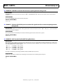
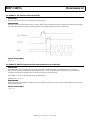
58. 03000373 - PLL Failure to Lock at Power-Up:
DESCRIPTION:
The PLL may fail to lock correctly to the SCLK input during power-up.
WORKAROUND:
Vdd/Vdd_a must be held low until after Vdd_io and SCLK_Vref are stable and within specification. Additionally, SCLK must be held high
or low until after Vdd/Vdd_a is stable and within specification. The following figure illustrates the workaround:
APPLIES TO REVISION(S):
1.1, 1.2, 2.0
59. 03000375 - DMA for link port to/from external memory may be blocked:
DESCRIPTION:
DMA between link ports and external memory may be blocked by an external port DMA. If the DMA sequences are concurrent,
transactions for the link port DMA to/from external memory may not occur at the expected rate and may even be blocked until the
completion of the external port DMA (internal to external or external to internal memory).
This problem occurs only for the following specific SCLKRAT settings:
SCLKRAT = 4, 6, 8, 10, or 12
WORKAROUND:
Divide large external port DMAs into multiple, smaller count DMAs to allow link port to/from external memory DMAs transactions to be
granted more frequently.
APPLIES TO REVISION(S):
1.1, 1.2, 2.0
NR002910Q | Page 28 of 29 | January 2008
ADSP-TS201S
Silicon Anomaly List
60. 03000376 - Link port receive to link port transmit DMA fails:
DESCRIPTION:
Link port receive to link port transmit DMA does not work properly. The counter of the link port receiver DMA channel updates
erroneously when the link transmit buffer is full.
WORKAROUND:
Do not use link port receive to link port transmit DMA. Use DMA from link port receiver to memory followed by DMA from memory to link
port transmitter to achieve the same data flow.
APPLIES TO REVISION(S):
1.1, 1.2
©2008 Analog Devices, Inc. All rights reserved. Trademarks and
registered trademarks are the property of their respective owners.
a
NR002910Q | Page 29 of 29 | January 2008
www.analog.com