1
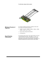
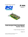
FuturePlus Systems Corporation
LOCAL BUS
Active Analysis Probe Users ManualFS2100 / FS2101
For Agilent Technologies Logic Analyzers
Revision 1.8
FuturePlus is a trademark of FuturePlus Systems Corporation
Copyright 1998 FuturePlus Systems Corporation
HOW TO REACH US
5
PRODUCT WARRANTY
6
Limitation of warranty
Exclusive Remedies
6
6
Assistance
6
INTRODUCTION
7
How to Use This Manual
7
ANALYZING THE PCI LOCAL BUS
8
Duplicating the Master Diskette
8
Accessories Supplied
8
Minimum Equipment Required
9
Signal Naming Conventions
9
Viewing the interrupts
10
Configuring the front panel switches and LEDs
10
Powering the PCI Active Analysis Probe
11
Connecting to the PCI Active Analysis Probe
Multiplexed versus Demultiplexed
32 bit PCI Demultiplexed
32 bit PCI Multiplexed
64 bit PCI Multiplexed
64 bit PCI Demultiplexed
11
12
12
12
13
13
USER PINS
14
Installing the PCI Active Analysis Probe
14
How to install a PCI add-in card into the extender card connector
15
Operation of the PCI add-in card
The Extender Card Connector
15
15
Setting up the Analyzer from the diskette
The PCI Inverse Assembler
16
17
2
The Format Menu
The STAT variable
The ADDR, ADDR_B , ADDR_C, DATA_B and DATA variables
The BUS_UT variable
The L_CMD variable
17
18
19
19
19
Theory of Operation
The Input Buffers
The Latching Buffers
The interface to the Logic Analyzer
The Clocking and Cycle bit Generation Logic
The Data Parity Checking Logic
20
20
21
21
21
22
STATE ANALYSIS
23
Installation Quick Reference
23
Using the front panel switches in state mode
23
Acquiring Data
24
The State Display
24
Error Messages
25
INVASM OPTIONS
25
Setting up the Analyzer to use the PC Mapper Inverse Assembler
25
Acquiring Data
25
The State Display with the PCI PC Mapper
26
Error Messages
27
PCI PC Mapping for memory transactions
27
Interrupt Vector Table
28
PCI PC Mapping - I/O Transactions
30
TIMING ANALYSIS
33
Installation Quick Reference
33
Timing Mode Skew
33
Using the Cycle bits and L_CMD lines
34
Demultiplexed versus Multiplexed
34
Acquiring Data
34
3
The Waveform Display
34
GENERAL INFORMATION
36
Characteristics
36
Analysis Probe Interface Compatibility
36
JTAG Boundary Scan
36
The PCI Present Pins
36
Standards Supported
36
Power Requirements
36
Logic Analyzer Required
36
Number of Probes Used
36
Minimum Clock Period (State)
37
Signal loading
37
Operations
37
Environmental Temperature
37
Altitude
37
Humidity
37
Testing and Troubleshooting
37
Servicing
37
Signal Connections
38
4
How to reach us
For Technical Support:
FuturePlus Systems Corporation
36 Olde English Road
Bedford NH 03110
TEL: 603-471-2734
FAX: 603-471-2738
On the web http://www.futureplus.com
For Sales and Marketing Support:
FuturePlus Systems Corporation
TEL: 719-278-3540
FAX: 719-278-9586
On the web http://www.futureplus.com
FuturePlus Systems has technical sales
representatives in several major countries. For an up
to date listing please see
http://www.futureplus.com/contact.html.
Agilent Technologies is also an authorized reseller of
many FuturePlus products. Contact any Agilent
Technologies sales office for details.
5
Product Warranty
This FuturePlus Systems product has a warranty against defects
in material and workmanship for a period of 1 year from the date
of shipment. During the warranty period, FuturePlus Systems
will, at its option, either replace or repair products proven to be
defective. For warranty service or repair, this product must be
returned to the factory.
For products returned to FuturePlus Systems for warranty
service, the Buyer shall prepay shipping charges to FuturePlus
Systems and FuturePlus Systems shall pay shipping charges to
return the product to the Buyer. However, the Buyer shall pay all
shipping charges, duties, and taxes for products returned to
FuturePlus Systems from another country.
FuturePlus Systems warrants that its software and hardware
designated by FuturePlus Systems for use with an instrument
will execute its programming instructions when properly installed
on that instrument. FuturePlus Systems does not warrant that
the operation of the hardware or software will be uninterrupted or
error-free.
Limitation of
warranty
The foregoing warranty shall not apply to defects resulting from
improper or inadequate maintenance by the Buyer, Buyersupplied software or interfacing, unauthorized modification or
misuse, operation outside of the environmental specifications for
the product, or improper site preparation or maintenance. NO
OTHER WARRANTY IS EXPRESSED OR IMPLIED.
FUTUREPLUS SYSTEMS SPECIFICALLY DISCLAIMS THE
IMPLIED WARRANTIES OF MERCHANTABILITY AND
FITNESS FOR A PARTICULAR PURPOSE.
Exclusive Remedies
THE REMEDIES PROVIDED HEREIN ARE BUYER’S SOLE
AND EXCLUSIVE REMEDIES. FUTUREPLUS SYSTEMS
SHALL NOT BE LIABLE FOR ANY DIRECT, INDIRECT,
SPECIAL, INCIDENTAL, OR CONSEQUENTIAL DAMAGES,
WHETHER BASED ON CONTRACT, TORT, OR ANY OTHER
LEGAL THEORY.
Assistance
Product maintenance agreements and other customer
assistance agreements are available for FuturePlus Systems
products. For assistance, contact the factory.
6
Introduction
The PCI Active Analysis Probe module provides a complete
interface between any PCI add-in slot and Agilent Logic
Analyzers. The Analysis Probe interface buffers and in state
mode latches and decodes all PCI cycle types and transactions.
The PCI Active Analysis Probe is a passive bus monitor which
does not assert any signals on the PCI bus. The PCI bus
signals are buffered and then terminated with 90k ohm/10pf
terminators so that they are impedance matched to the logic
analyzer. Since the PCI Active Analysis Probe does contains
high speed low skew buffers very little skew is introduced.
The configuration software on the diskette sets up the format
specification menu of the logic analyzer for compatibility with
your PCI bus. When the state configuration file is loaded, an
inverse assembler is also loaded which decodes PCI
transactions into easy to read mnemonics.
How to Use This
Manual
This manual is organized to help you quickly find the information
you need.
•
Analyzing the PCI Local Bus chapter introduces you to the
PCI Active Analysis Probe and lists the minimum equipment
required and accessories supplied for PCI bus analysis.
•
The State Analysis chapter explains how to configure the
PCI Active Analysis Probe to perform state analysis on your
PCI bus.
•
The Timing Analysis chapter explains how to configure the
PCI Active Analysis Probe to perform timing analysis on your
PCI bus.
•
The General Information chapter provides some general
information including the operating characteristics for the
PCI Active Analysis Probe module and the cable header
pinout.
7
Analyzing the PCI Local Bus
This chapter introduces you to the PCI Active Analysis Probe
and lists the minimum equipment required and accessories
supplied for PCI Local Bus analysis. This chapter also contains
information that is common to both state and timing analysis.
Duplicating the
Master Diskette
Before you use the PCI Analysis Probe software, make a
duplicate copy of the master diskette. Then store the master
diskette and use the back-up copy to configure your logic
analyzer. This will help prevent the possibility of losing or
destroying the original files in the event the diskette wears out, is
damaged, or a file is accidentally deleted.
To make a duplicate copy, use the Duplicate Diskette operation
in the disk menu of your logic analyzer. For more information,
refer to the reference manual for your logic analyzer.
Accessories
Supplied
The PCI Active Analysis Probe product consists of the following
accessories:
•
The Analysis Probe interface hardware, which includes the
interface circuit module.
•
one jumper which is installed on the circuit module.
•
The inverse assembly and configuration software on a 3.5
inch diskette.
•
11 cables
•
This operating manual
8
The PCI Active Analysis Probe module
Minimum Equipment
Required
Signal Naming
Conventions
The minimum equipment required for analysis of a PCI Local
Bus consists of the following equipment:
•
1660A/C, 1661A/C, 1662A/C, 16550A, 16554A, 16555A,
16556A, 1670A, 1671A, 1672A
•
The PCI Active Analysis Probe Product
•
A PCI target bus
This operating manual uses the same signal notation as the PCI
LOCAL BUS SPECIFICATION - REVISION 2.1. That is, a #
symbol at the end of a signal name indicates that the signals
active state occurs when it is at a low voltage. The absence of a
# symbol indicates that the signal is active at a high voltage.
9
Viewing the
interrupts
Pod 1 channel 0 can be configured to view any one of the four
PCI interrupts. Move the jumper so that it corresponds to the
desired interrupt and that interrupt line will be routed to POD 1
channel 0. The jumper and interrupt stake pins are clearly
labeled and are located under POD 7.
Interrupt Jumper
Pod 0 Channel 1 INT
Configuring the front
panel switches and
LEDs
I
I
I
I
N
N
N
N
T
T
T
T
A
B
C
D
Switch
Setting
LED
Parity On
Parity Checking
enabled
ON
Parity On
Parity checking
disabled
OFF
No Wait
No Wait cycles
acquired
ON
No Wait
All Wait cycles
acquired
OFF
No Idle
No Idle cycles
acquired
ON
No Idle
All Idle cycles
acquired
YES
TDO/TDI
TDO connected to
TDI
No LED, switch in
rightmost position
TDO/TDI
TDO not connected
to TDI
No LED, switch in
leftmost position
State/Timing
State
ON
State/Timing
Timing
OFF
10
Parity On
No Wait
No Idle
State
1
ON
2
Parity On
3
No Wait
4
No Idle
TD0-TD1
State
Timing
FuturePlus
Systems
PCI Active Analysis Probe front panel
Powering the PCI
Active Analysis
Probe
The active circuitry on the PCI Active Analysis Probe module
gets its power from the logic analyzer PODs. No power is taken
from the target PCI system. Please Note: If the Analysis
Probe is plugged into the PCI bus and the logic analyzer is
not connected or powered up the input buffers on the
Analysis Probe will create a low impedance path to ground
thus inhibiting the PCI local bus and any card in the
extender card connector from working.
The Logic analyzer must be connected and powered on for
the PCI Active Analysis Probe to work properly. ONLY
connect to the analysis probe headers 7-10 if you are doing
64 bit analysis. Latchup may occur on the 64 bit interface
parts if they are powered on and not on a 64 bit bus.
Connecting to the
PCI Active Analysis
Probe
The following explains how to connect the logic analyzer to the
PCI Active Analysis Probe for either state or timing analysis:
1. Remove the probe tip assemblies from the logic
analyzer cables.
2. Plug the logic analyzer cables into the PCI Active
Analysis Probe cable headers as shown in the
appropriate following tables.
11
Multiplexed versus
Demultiplexed
The PCI Local Bus specification specifies that the AD lines and
the C/BE lines carry different information at different times. This
is referred to as multiplexed. Using the extra clocking features
and additional pods of the logic analyzer the AD lines can be
demultiplexed. By using the PCI Active Analysis Probe in
demultiplexed mode the address of the transaction can be held
throughout the transaction thus making triggering and
performance analysis easier.
Please note that the C/BE lines have been demultiplexed on the
PCI Active Analysis Probe. Thus the command is held through
the transaction and no additional clocking or pods is required.
The latched command L_CMD signals are on pod 1 channels
10-7.
32 bit PCI Demultiplexed
32 bit PCI Multiplexed
Logic Analyzer
PCI Active Analysis
Probe
Master POD 1
Header 1
Comment
POD 2
Header 2
POD 3
Header 3
POD 4
Header 4
POD 5
Header 5
16554/5/6/7
expander
card POD 1
POD 6
Header 6
16554/5/6/7
expander
card POD 2
Logic Analyzer
PCI Active Analysis
Probe
Master POD 1
Header 1
POD 2
Header 2
POD 3
Header 3
POD 4
Header 4
12
Comment
64 bit PCI Multiplexed
Logic Analyzer
PCI Active Analysis
Probe
Comment
Master POD 1
Header 1
POD 2
Header 2
POD 3
Header 3
POD 4
Header 4
POD 5
Header 7
16554/5/6/7
expander
card POD 1
POD 6
Header 8
16554/5/6/7
expander
card POD 2
POD 7
Header 11
16554/5/6/7
expander
card POD 3
16550 expander
card Pod 1
64 bit PCI Demultiplexed
Logic Analyzer
PCI Active Analysis
Probe
Comment
Master POD 1
Header 1
POD 2
Header 2
POD 3
Header 3
POD 4
Header 4
POD 5
Header 5
16554/5/6/7
expander
card POD 1
POD 6
Header 6
16554/5/6/7
expander
card POD 2
POD 7
Header 7
16554/5/6/7
expander
card POD 3
16550 expander
card Pod 1
POD 8
Header 8
16554/5/6/7
expander
card POD 4
16550 expander
card Pod 2
13
POD 9
Header 9
16554/5/6/7
expander 2
card POD 1
16550 expander
card Pod 3
POD 10
Header 10
16554/5/6/7
expander
card POD 2
16550 expander
card Pod 4
POD 11
Header 11
16554/5/6/7
expander
card POD 3
16550 expander
card Pod 5
USER PINS
PCI Active Analysis Probe Header 4 contains 8 User Defined
pins. These pins are available to the user to connect whatever
additional signals the users wishes to view along with the PCI
bus. These pins are located below POD 3 on the PCI Active
Analysis Probe module and clearly marked. These user pins
are available on the logic analyzer on POD 11 channels 15 thru
8.
These pins may be used to connect the individual IDSEL signals
from other PCI slots or the bus grant signals from the PCI bus
arbitration logic.
Installing the PCI
Active Analysis
Probe
The PCI Active Analysis Probe can be installed in any slot of the
PCI Local bus. The following steps explain how to install the PCI
Active Analysis Probe into the PCI Local bus.
1. Install the logic analyzer cables as described in the
previous section.
2. Power off the PCI target. Align the PCI module with the
appropriate slot on the target system and plug the
module into the PCI connector. Power on the logic
analyzer and then power on the target.
If your PCI Local bus is 32 bits the upper portion of the edge
connector will not be inserted into any connector. This will not
affect the modules operation on a 32-bit PCI Local bus.
14
How to install a PCI
add-in card into the
extender card
connector
The card edge connector of the PCI Active Analysis Probe
module can accommodate one 32 or 64 bit 5V OR 3V PCI add in
card. The extender card connector is either a 3V or 5V
connector depending on how the board was ordered and
configured at the factory.
Simply align the module with the connector and gently push the
module in until it is seated in the connector. There is sufficient
clearance for the add-in card front plate. The PCI Active
Analysis Probe/PCI add-in card combination can then be
installed in any slot of the PCI Local bus. For mechanical
stability the PCI Active Analysis Probe front plate should be
secured to the PCI target system chassis.
When removing the PCI add-in card from the card edge extender
connector grasp the PCI Active Analysis Probe with one hand
and the PCI add-in card with the other. Gently rock the PCI addin card until it is free from the connector.
Operation of the PCI
add-in card
The nature of an extender card is that it extends the etch length
of the bus. Due to the sensitivity of most PCI designs, extending
the etch length can interfere with the PCI add-in card operation.
Operation of the PCI add-in card when installed in the card edge
extender connector is not guaranteed. Please check your
system design if you experience failures due to poor signal
fidelity.
The etch from the PCI local bus is routed directly from the PCI
local bus to the extender card connector. Although the etch is
connected to the input of the PCI Active Analysis Probe input
buffers, the extender card connector is NOT buffered from the
PCI local bus.
Please Note: If the Analysis Probe is plugged into the PCI
bus and the logic analyzer is not powered up, the input
buffers on the Analysis Probe will create a low impedance
path to ground thus inhibiting the PCI local bus and any
card in the extender card connector from working.
The Extender Card
Connector
The PCI bus is extended up from the gold fingers to the input of
the IDT162260 buffers. From the buffer input the etch goes
directly to the extender card connector. The buffer input
provides a clamping diode. The etch is extended approximately
5 inches from the gold fingers and is on the inner most layer of
the board. There are no via’s on this inner layer in order to give
this etch a direct route.
One issue that has been encountered with using the extender
card connector is that the buffers need power in order to provide
a high impedance to the signal. This means that the logic
analyzer must be attached to the Analysis Probe and powered
up. The PCI Active Analysis Probe module itself is a universal
card. It can operate in either a 5V or 3V PCI system.
15
Setting up the
Analyzer from the
diskette
The logic analyzer can be configured for PCI analysis by loading
the PCI configuration file. Loading this file will load the PCI
Local bus inverse assembler and configure your logic analyzer.
To load the configuration and inverse assembler:
1. Install the PCI Active Analysis Probe software flexible
diskette in the disk drive of the logic analyzer.
2. Configure the menu to “Load” the analyzer with the
appropriate configuration file (see table below).
3. Execute the load operation to load the file into the logic
analyzer that the PCI Active Analysis Probe module is
connected to. DO NOT SELECT ALL OR SYSTEM.
Logic Analyzer
File
Comment
nam
e for
State
Anal
ysis
166x
P32M_66
0
32 bit Multiplexed - Analysis Probe PODS 1-4
connect to Logic Analyzer PODS 1-4
166x
P32D_66
0
32 bit Demultiplexed - Analysis Probe PODS
1-6 connect to Logic Analyzer PODS 1-6
166x
P64M_66
0
64-bit Multiplexed- Analysis Probe PODS 14,7,8,11 to Logic Analyzer PODS 1-7
16550A
P32M_55
0
32 bit Multiplexed- Analysis Probe PODS 1-4
connect to Logic Analyzer PODS 1-4
16550A
P32D_55
0
32 bit Demultiplexed - Analysis Probe PODS
1-6 connect to Logic Analyzer PODS 1-6
16550A
P64AD55
0
32 bit address Demultiplexed and 64 bit data
Analysis Probe PODS 1-6,7,8 and 11
connect to Logic Analyzer PODS 1-6 on
the Master card and 1-3 on the Slave card
respectively.
16550A
P64M_55
0
64-bit Multiplexed - Analysis Probe PODS 14,7,8,11 connect to LA PODS 1-6 on the
Master card and Pod 1 on the Slave card
respectively
16550A
P64D_55
0
64 bit Demultiplexed- Analysis Probe PODS
1-11 connect to Logic Analyzer PODS 1-6
on the Master card and PODS 1-5 on the
Slave Card respectively
1655x,167x
P32M_55
5
32 bit Multiplexed - Analysis Probe PODS 1-4
connect to Logic Analyzer PODS 1-4
16
1655x,1670/71
P32D_55
5
32 bit Demultiplexed - Analysis Probe PODS
1-6 connect to PODS 1-4 on the Master
card and 1-2 on the Slave card 1-2
respectively (PODS 1-6 on the 1670/71)
1655x,1670
P64M_55
5
64-bit Multiplexed - Analysis Probe PODS 14,7,8,11 connect to Logic Analyzer PODS
1-4 on the Master card and PODS 1-3 on
the Slave Card respectively (PODS 1-7
on the \1670)
1655x
P64D_55
5
64 bit Demultiplexed - Analysis Probe PODS
1-11 connect to Logic Analyzer PODS 14 on the Master card, 1-4 on the lower
slave card (positioned below the master
card in the mainframe) and PODS 1-3 on
the slave card positioned above the
master card in the mainframe respectively
1655x
P64AD55
5
32 bit address Demultiplexed and 64 bit data
Analysis Probe PODS 1-6,7,8 and 11 to
Logic Analyzer PODS 1-4 on the Master
card, 1-4 on the lower slave card
(positioned below the master card in the
mainframe) and POD 1 on the slave card
positioned above the master card in the
mainframe respectively
The PCI Inverse
Assembler
The PCI Active Analysis Probe Inverse Assembler file IAP64E is
automatically loaded into the logic analyzer when the
configuration file is loaded. If the Inverse Assembler does not
appear on the state listing screen select the base of the label
DATA. From the menu that appears select INVASM. The
Inverse Assembler is only for use in state mode.
The Format Menu
The PCI Active Analysis Probe diskette sets up the format menu
to include all of the signals that are presented to the logic
analyzer. This format is the same for both Timing and State
Analysis. the labels STAT, DATA , DATA_B, ADDR and
ADDR_B are required in order run the Inverse Assembler. They
should not be changed or deleted.
17
The STAT variable
The STAT variable is used by the PCI inverse assembler to
decode PCI bus transactions. It should not be changed or
deleted from the format menu. The signals that make up the
STAT variable are listed in the following table. The STAT
variable can be useful to set up SYMBOLS since it contains all of
the key PCI control and status signals.
STAT Variable
PCI Bus Signal Name
Bit 29
C/BE7
Bit 28
C/BE6
Bit 27
C/BE5
Bit 26
C/BE4
Bit 25
REQ64#
Bit 24
AVALID_L
Bit 23
WNODEV_L
Bit 22
ACK64# (DATA64)
Bit 21
TABORT_L
Bit 20
DVALID_L
Bit 19
WTARGET_L
Bit 18
IWINITI_L
Bit 17
RETRY_L
Bit 16
SERR#
Bit 15
IDLE_L
Bit 14
PVALID_L
Bit 13
MABORT_L
Bit 12
CPERR_L
Bit 11
STOP#
Bit 10
DEVSEL#
Bit 9
L_CM3
Bit 8
L_CM2
Bit 7
L_CM1
Bit 6
L_CM0
Bit 5
C/BE3
Bit 4
C/BE2
Bit 3
C/BE1
Bit 2
C/BE0
Bit 1
RESET#
Bit 0
PERR#
18
The ADDR, ADDR_B ,
ADDR_C, DATA_B and
DATA variables
The BUS_UT variable
The L_CMD variable
The ADDR, ADDR_B, ADDR_C, DATA_B and DATA variables
are defined in the format menu and used to pass the AD line
information to the Inverse Assembler during state analysis. They
are mapped as shown in the below table. These variables
should not be changed or deleted from the format Menu.
Mode
ADDR
ADDR_B
ADDR_C
DATA
DATA_
B
32 BIT
MUX
LOWER
32 AD
LINES
NOT
USED
NOT USED
LOWER
32 AD
LINES
NOT
USED
32 BIT
DEMUX
LOWER
32 AD
LINES
- DATA
LOWER 32
AD ADDRESS
NOT USED
LOWER
32 AD
LINES DATA
NOT
USED
64 BIT
MUX
LOWER
32 AD
LINES
- DATA
NOT
USED
NOT USED
LOWER
32 AD
LINES DATA
UPPER
32 AD
LINES
64 BIT
DEMUX
LOWER
32 AD
LINES
- DATA
LOWER 32
AD ADDRESS
UPPER 32
AD LINES ADDRESS
LOWER
32 AD
LINES DATA
UPPER
32 AD
LINES
The Bus Utilization BUS_UT variable is made up of the following
cycle bits: WNODEV, ADVALID, TABORT, DVALID, WTARGET,
WINITI, RETRY, IDLE, MABORT. The list of symbols defined
for this variable are the signal names themselves. This is a
convenient grouping that helps make triggering and performance
analysis easier.
This variable is the C/BE[3:0] lines latched with the first rising
edge of the PCI clock with FRAME# asserted. These signals are
held until the end of the transaction. They indicated the
command that is being transmitted on the PCI Local bus. Below
is the encoding of these signals and the symbols defined for the
L_CMD variable. These encodings can also be found in the PCI
Specification.
Symbol
L_CMD encoding
INTACK
0000
SPEC_CYC
0001
I/O_RD
0010
I/O_WR
0011
19
Theory of Operation
RESRVD
0100
RESRVD
0101
MEM_RD
0110
MEM_WR
0111
RESRVD
1000
RESRVD
1001
CON_RD
1010
CON_WR
1011
MEMRDM
1100
DAC_CY
1101
MEMRDL
1110
MEMWRI
1111
I/O_XACTIONS
001X
MEM_XACTIONS
011X
CONFIG_XACTIONS
101X
The PCI Active Analysis Probe is a universal PCI short card that
attaches to Agilent logic analyzers. The Analysis Probe has five
major parts:
1. The input buffers
2. The latching buffers
3. The interface to the logic analyzer
4. The clocking and cycle bit generation logic
5. The extender card connector
The Input Buffers
The input buffers present a single electrical load on the PCI bus
and are made up of IDT162260 tri-port buffers. The PCI clock is
buffered by a Motorola 807 high speed clock buffer.
When the Analysis Probe is in Timing mode output Port 2 of the
tri-port buffers goes directly to the logic analyzer input
terminators. When in State mode output Port 2 is tri-stated.
Output port 1 is always enabled and goes to the latching buffers.
20
The Latching Buffers
The latching buffers are used only for state mode. The entire
PCI bus (except the clock) is latched in these buffers on the
rising edge of the PCI clock. The input to the latching buffers is
output port 1 from the input buffers. The latching buffers are IDT
162511 latching buffers with party generation. These buffers are
tri-stated in timing mode. In state mode their outputs go directly
to the logic analyzer input terminators.
The User pin signals are not latched.
The interface to the
Logic Analyzer
The input to the logic analyzer consists of 3 parts.
1. The RC terminators (90 ohm/10pf)
2. The 40 pin headers
3. The 40 pin cables
The user is instructed to remove the probe tip assemblies from
the logic analyzer headers. The 40 pin logic analyzer headers
then go directly the 40 pin headers of the Analysis Probe
provided cables. Any unused cables can be removed from the
Analysis Probe.
The logic analyzer provides the power to the onboard logic. No
power is obtained from the target.
The Clocking and Cycle
bit Generation Logic
The master clock is controlled by the front panel switches and is
generated by the on-board CPLD devices. When the user has
loaded the DEMULTIPLEXED configuration file an additional
Slave clock is added. This Slave clock is the falling edge of the
Analysis Probe generated AVALID signal. This signal asserts
with the first assertion of FRAME# and the rising edge of the PCI
clock. All of the PCI cycle bits are generated based on the
latched version of the PCI control signals. Their meaning is
listed in the following table.
Cycle bit name
Function
EOFT_L - End of Transaction
True for one clock cycle and indicates
the last cycle of a transaction
CPERR_L - Calculated Parity
Error
True for one clock cycle and indicates
that the on board parity logic has
detected a parity that is different than
the parity transmitted on the bus.
Please note that the Parity Checking
switch must be in the ON position.
MABORT_L - Master Abort
True when a Master Abort condition has
been detected. Five clock cycles on a
single data transfer with no DEVSEL
assertion and six clock cycles on a
multi-beat transfer with no DEVSEL
asserted. Remains true for one clock
cycle.
21
PVALID_L - Parity Valid
True for the cycles in which parity is
being transmitted on the PCI bus.
IDLE_L - Idle cycle
True when the bus is IDLE. False when
the bus is busy.
DVALID_L - Data Valid
True when data is being transferred on
the PCI bus.
WINITI_L - Master Initiated
Wait State
True when a wait state is being initiated
by the master
WTARGET_L - Target
Initiated Wait State
True when a wait state is being initiated
by the target
RETRY_L - Retry
True when a retry condition has been
detected on the PCI bus
TABORT_L - Target Abort
True when a Target Abort condition has
been detected on the PCI bus. This
signal is true for one clock bit.
WNODEV_L - Wait state
caused by no assertion of
DEVSEL#
True when a wait state has been
caused by no assertion of DEVSEL#.
GNT_L - The Grant signal for
that slot
In State Mode this signal is latched and
held until end of transaction. Useful as
a store qualifier.
In timing mode the GNT# from the PCI
bus is passed through to the logic
analyzer.
The Data Parity
Checking Logic
L_CMD - The latched
command lines
The C/BE signals latched during the
command /address phase and held until
end of transaction.
AVALID_L - Address Valid
True on the first assertion of FRAME#
and the rising edge of the PCI clock.
True for one cycle except on Dual
Address cycles when it is true for two
cycles.
Parity checking is only available in STATE Mode and is
controlled by the PARITY ON switch on the front panel. The
parity generation is done by the IDT 162511 latching buffers.
Only data parity is generated and then checked against the data
parity that is transferred on the bus. If they are not the same
then the signal CPERR_L will be asserted on the cycle that the
parity is valid. This signal will remain valid for one clock tic.
22
State Analysis
This chapter explains how to configure the PCI Active Analysis
Probe to perform state analysis on the PCI Local Bus. The
configuration software on the flexible diskette sets up the format
specification menu of the logic analyzer for compatibility with the
PCI Local Bus. The next chapter explains how to configure the
PCI Active Analysis Probe to perform timing analysis.
Installation Quick
Reference
The following procedure describes the major steps required to
perform measurements with the PCI Active Analysis Probe
module.
1. After removing the probe tip assemblies, plug the logic
analyzer cables into the Analysis Probe cable headers.
See page 11 of this manual for details.
2. Set the STATE/TIMING switch to STATE. The State
LED will be lit.
3. Power off the target. Install the PCI Active Analysis
Probe module into a slot in the target PCI Local bus.
Then power on the target.
Load the logic analyzer configuration file by loading the
appropriate file from the Analysis Probe interface diskette. See
page 16 of this manual for details.
Using the front panel
switches in state
mode
The front panel switches are only useful in STATE MODE. They
are clearly marked on the front panel.
•
The Parity On switch controls parity checking. If the Parity
On LED is lit then parity checking will be done.
•
The No Wait switch controls the acquisition of WAIT cycles.
If the No Wait LED is lit then no wait cycles will be acquired.
•
The No Idle switch controls the acquisition of IDLE cycles. If
the No Idle LED is lit then NO IDLE cycles will be acquired.
•
The TDO-TDI switch from the top connects TDO to TDI. If
the switch is to the rightmost position TDO is connected to
TDI.
•
The State/Timing switch controls the on board latches.
When the State LED is lit then the PCI Active Analysis Probe
is in State mode.
Refer to page 10 for more details on the LEDs and switches.
23
Acquiring Data
Touch RUN and, as soon as there is activity on the bus, the logic
analyzer will begin to acquire data. The analyzer will continue to
acquire data and will display the data when the analyzer memory
is full, the trigger specification is TRUE or when you touch
STOP.
The logic analyzer will flash “Slow or Missing Clock” when the
data is not being transmitted across the bus.
The State Display
Captured data is as shown in the following figure. The below
figure displays the state listing after disassembly. The inverse
assembler is constructed so the mnemonic output closely
resembles the actual commands, status conditions, messages
and phases specified in the PCI Local Bus specification.
Symbols have also been defined to help aid in analysis. The
non-disassembled state listing displays PCI bus mnemonics in
addition to data. All data is displayed in hex. One exception is
the decode of the address for a CONFIGURATION READ or a
CONFIGURATION WRITE transaction. The Function (FUNC=)
and Bus (BUS=) data is displayed in decimal.
24
Error Messages
The following error messages are reported by the PCI
inverse assembler.
ERROR-NO DEVICE SELECTED
This error is displayed during a non special cycle data phase
when IRDY and TRDY are asserted and DEVSEL is not
asserted.
ERROR DEVSEL ASSERTED
This error is displayed during a special cycle data phase if
DEVSEL is asserted.
SYSTEM ERROR
This error is displayed anytime SERR# is asserted.
INVASM OPTIONS
The INVASM OPTIONS feature is not included with the PCI
Active Analysis Probe software. The same or better capability
for post processing acquired data can be achieved using the
16505A Pattern Filters.
Setting up the
Analyzer to use the
PC Mapper Inverse
Assembler
After the configuration file is loaded the PCI PC Mapper software
can be loaded:
1. Install the PCI Analysis Probe software flexible diskette
in the disk drive of the logic analyzer.
2. Configure the menu to “Load” the analyzer that is
connected to the PCI Active Analysis Probe with the file
names IAP64EXM.
3. Execute the load operation to load the file into the logic
analyzer.
Acquiring Data
Data can be acquired by touching the RUN button. As soon as
there is activity on the bus, the logic analyzer will begin to
acquire data. The analyzer will continue to acquire data and will
display the data when the analyzer memory is full, the trigger
specification is TRUE or when you touch STOP.
The logic analyzer will flash “Slow or Missing Clock” if the PCI
Clock signal is not being detected by the logic analyzer. In this
case, check the logic analyzer to PCI Active Analysis Probe
connection (refer to your User’s Manual).
25
The State Display
with the PCI PC
Mapper
Captured data is as shown in the following figure. The first figure
displays the state listing after disassembly. The PCI PC Mapper
is constructed so the mnemonic output closely resembles the
actual commands, status conditions, messages and phases
specified in the PCI Local Bus specification. Symbols have also
been defined to help aid in analysis. The non-disassembled
state listing displays PCI bus mnemonics in addition to data. All
data is displayed in hex. One exception is the decode of the
address for a CONFIGURATION READ or a CONFIGURATION
WRITE transaction. The Function (FUNC=) and Bus (BUS=)
data is displayed in decimal.
The above display data using the PCI Inverse Assembly
software without the PCI PC Mapper functionality is shown as
follows.
26
Error Messages
PCI PC Mapping for
memory transactions
The error messages reported by the PCI PC Mapper are the
same as those reported with the standard non mapper version of
the PCI Inverse Assembler.
This section lists the addresses, the commands and the
corresponding mapping done by the PCI PC Mapper software.
For information on the standard PCI configuration register
mapping please refer to the PCI Local Bus Specification Rev 2.0.
Address bits 23-0
greater than 0FFFFFH
0FFFFF-0E0000H
0DFFFF-0C0000H
0BFFFF-0A0000H
09FFFF-000400H
0003FF-000000H
27
PC Mapper output
System Memory
System BIOS
ROM Scan
Video Memory
System Memory
See Interrupt Vector Table
Interrupt Vector
Table
Address bits
23-0
0003C4H
000200H
0001E0H
0001DCH
0001D8H
0001D4H
0001D0H
0001CCH
0001C8H
0001C4H
0001C0H
0001A0H
00019CH
000180H
00012CH
000128H
00011CH
000118H
000110H
00010CH
000108H
000104H
000100H
000080H
00007CH
000078H
000074H
000070H
00006CH
000068H
000064H
000060H
00005CH
000058H
000054H
000050H
00004CH
000048H
000044H
000040H
00003CH
000038H
000034H
000030H
00002CH
000028H
000024H
000020H
00001CH
000018H
000014H
000010H
00000CH
28
PC Mapper output
INT #F1-FF USER PROGRAMS
INT #80-F0 BASIC
INT #78-7F USER PROGRAMS
INT #77 IRQ15
INT #76 IRQ14
INT #75 IRQ13
INT #74 IRQ12
INT #73 IRQ11
INT #72 IRQ10
INT #71 IRQ9
INT #70 IRQ8
INT #68-6F RESERVED
INT #67 EXP MEM MANG
INT #60-66 USER PROGRAMS
INT #4B-5F RESERVED
INT #4A USER RTC ALARM
INT #47-49 RESERVED
INT #46 HD DISK #1 PARAM
INT #44-45 RESERVED
INT #43 VIDEO CHAR TABLE
INT #42 EGA BIOS
INT #41 HD DISK #0 PARAM
INT #40 FLOPPY DISK ISR
INT #20-3F RESERVED DOS
INT #1F VIDEO CHAR TABLE
INT #1E FLOPPY PARAMS
INT #1D AVAILABLE
INT #1C AVAILABLE
INT #1B KEYBOARD BREAK
INT #1A RTC ISR
INT #19 BOOSTRAP LOADER
INT #18 ROM BASIC
INT #17 LPT PRINTER BIOS
INT #16 KEYBOARD BIOS
INT #15 SYS SERVICE BIOS
INT #14 SERIAL PORT BIOS
INT #13 FLOPPY DISK BIOS
INT #12 MEM SIZE INT
INT #11 EQUIP LIST
INT #10 VIDEO BIOS
INT #0F IRQ7 LPT1
INT #0E IRQ6 FLOPPY DISK
INT #0D IRQ5 LPT2
INT #0C IRQ4 SERIAL #1
INT #0B IRQ3 SERIAL #2
INT #0A IRQ2 SLAVE INT
INT #09 KEYBOARD
INT #08 IRQ0 SYS TIMER
INT #07 NUM COPROCESSOR
INT #06 INVALID OPCODE
INT #05 PRINT SCREEN
INT #04 OVERFLOW DETECT
INT #03 BREAKPOINT TRACE
000008H
000004H
000000H
29
INT #02 NMI
INT #01 SINGLE STEP
INT #00 DIVIDE BY ZERO
PCI PC Mapping - I/O
Transactions
Address bits
23-0
0000H
0001H
0002H
0003H
0004H
0005H
0006H
0007H
0008H
0009H
000AH
000BH
000CH
000DH
000EH
000FH
0018H
001AH
0020H
0021H
0040H
0042H
0043H
0044H
0047H
0060H
0061H
0064H
0070H
0071H
0074H
0075H
0076H
0081H
0082H
0083H
0087H
0089H
008AH
008BH
008FH
0090H
0091H
0092H
0094H
0096H
00A0H
00A1H
00C0H
00C2H
00C4H
00C6H
00C8H
30
PC Mapper output
MSTR DMA CH 0
MSTR DMA CH 0
MSTR DMA CH 1
MSTR DMA CH 1
MSTR DMA CH 2
MSTR DMA CH 2
MSTR DMA CH 3
MSTR DMA CH 3
MSTR DMA STAT REG
UNKNOWN IO DEVICE
MSTR DMA MASK REG
MSTR DMA MODE REG
MSTR DMA CLR BYTE PTR
MSTR DMA MSTR CLEAR
MSTR DMA CLEAR MASK
MSTR DMA WRT MASK
MSTR DMA CH EXT FUNCT REG
MSTR DMA EXT FUNCT
MSTR INT REQ REG
MSTR INT REQ REG2
INTERVAL TIMER TIMER 0
INTERVAL TIMER SPKR TIMER
INTRVAL TIMER #1 CNTRL
INTERVL TIMER #2 WATCHDOG
INTERVAL TIMER #2 CNTRL
KEYBOARD/MOUSE DATA PORT
SYSTEM CONTOL PORT B
KEYBOARD/MOUSE CMD PORT
RTC/CMOS RAM ADDR PORT
RTC/CMOS RAM DATA PORT
EXT CMOS RAM ADDR PORT
EXT CMOS RAM ADDR PORT
EXT CMOS RAM DATA PORT
CH 2 DMA PAGE REGISTER
CH 3 DMA PAGE REGISTER
CH 1 DMA PAGE REGISTER
CH 0 DMA PAGE REGISTER
CH 6 DMA PAGE REGISTER
CH 7 DMA PAGE REGISTER
CH 5 DMA PAGE REGISTER
CH 4 DMA PAGE REGISTER
ARB CNTRL POINT REG
FEEDBACK REG
SYSTEM CONTROL PORT A
SYS SETUP/CARD ENABLE REG
ADAPTOR SETUP/ENABLE REG
SLAVE INTERRUPT CNTRLR
SLAVE INTERRUPT CNTRLR
SLAVE DMA CH4 MEM ADDR
SLAVE DMA CH4 TRANS COUNT
SLAVE DMA CH5 MEM ADDR
SLAVE DMA CH5 TRANS COUNT
SLAVE DMA CH6 MEM ADDR
00CAH
00CCH
00CEH
00D0H
00D4H
00D6H
00D8H
00DAH
00DCH
00DEH
00E0H
00E1H
00F1H
00F8H
00F9H
00FAH
00FBH
00FCH
0100H
0101H
0102H
0103H
0104H
0105H
0106H
0107H
0278H
0279H
027AH
02F8H
02F9H
02FAH
02FBH
02FDH
02FEH
02FFH
0378H
0379H
037AH
03B4H
03B5H
03BAH
03BCH
03BDH
03BEH
03C0H
03C1H
03C2H
03C3H
03C4H
03C5H
03C6H
03C7H
03C8H
03C9H
SLV DMA CH6 TRANS COUNT
SLAVE DMA CH7 MEM ADDR
SLAVE DMA CH7 TRANS COUNT
SLV DMA STATUS REG CH 4-7
SLV DMA MASK REG CH 4-7
SLAVE DMA MODE REG CH 4-7
SLAVE DMA CLEAR BYTE PNTR
SLAVE DMA MASTER CLEAR
SLV DMA CLR MASK CH 4-7
SLAVE DMA WRITE MASK REG
IBM MODELS - ENCODE REG
IBM MODELS - ENCODE REG
NUMERIC COPROCESSOR RESET
NUMERIC COPROCESSOR PORT
NUMERIC COPROCESSOR PORT
NUMERIC COPROCESSOR PORT
NUMERIC COPROCESSOR PORT
NUMERIC COPROCESSOR PORT
ADAPTER CARD POS REG 0
ADAPTER CARD POS REG 1
SYS BD/ADP CD POS REG 2
SYS BD/ADP CD POS REG 3
ADAPTER CARD POS REG 4
ADAPTER CARD POS REG 5
ADAPTER CARD POS REG 6
ADAPTER CARD POS REG 6
PARALLEL PORT 3 DATA PORT
PARALLEL PORT 3 STAT PORT
PARALLEL PORT 3 CMD PORT
SERIAL PORT 2 XMIT/REC
SER PORT 2 DIV LATCH/INT
SERIAL PORT 2 INT ID REG
SERIAL PORT 2 CNTRL REG
SERIAL PORT 2 MODEM CNTRL
SERIAL PORT 2 MODEM STAT
SERIAL PORT 2 SCRTCH REG
PARALLEL PORT 2 DATA PORT
PARALLEL PORT 2 STAT PORT
PARALLEL PORT 2 CMD PORT
VGA CRT CNTRLR ADDR REG
VGA CRT CNTRLR DATA REG
VGA STAT 1/FEATURE CNTRL
PARALLEL PORT 1 DATA PORT
PARALLEL PORT 1 STAT PORT
PARALLEL PORT 1 CMD PORT
VGA ATTRIBUTE CNTRLR ADDR
VGA ATTRIBUTE CNTRLR DATA
VGA OUTPUT/STAT REG
VGA VIDEO SUBSYSTM ENABLE
VGA SEQUENCER ADDR REG
VGA SEQUENCER DATA REG
VIDEO DAC PEL MASK
VIDEO DAC PAL ADDR/STAT
VIDEO DAC PAL ADDR/WRITE
VIDEO DAC PALETTE DATA
31
03CAH
03CCH
03CEH
03CFH
03D4H
03D5H
03DAH
03F0H
03F1H
03F2H
03F4H
03F5H
03F7H
03F8H
03F9H
03FAH
03FBH
03FCH
03FDH
03FEH
03FFH
0680H
VGA FEATURE CONTOL REG
VGA MISC OUTPUT REG
VGA GRAPHICS CNTRLR ADDR
VGA GRAPHICS CNTRLR ADDR
VGA CRT CNTRLR ADDR REG
VGA GRAPHICS CNTRLR DATA
VGA COLOR STAT 1/FEATURE
FLOPPY STATUS REG A
FLOPPY STATUS REG B
FLOPPY DIGITAL OUTPUT REG
FLOPPY DISK CNTRLR STAT
FLOPPY DISK CNTRLR DATA
FLOPPY CONFIG CONTROL REG
SERIAL PORT 1 XMIT/RCV BUF
SER PORT 1 DIV LATCH/INT
SERIAL PORT 1 INT ID/FIFO
SERIAL PORT 1 LINE CNTRL
SERIAL PORT 1 MODEM CNTRL
SERIAL PORT 1 STAT REG
SERIAL PORT 1 MODEM STAT
SERIAL PORT 1 SCRATCH REG
MANUFCTURNG CHCKPNT PORT
32
Timing Analysis
Installation Quick
Reference
The following procedure describes the major steps required to
perform timing analysis measurements with the PCI Active
Analysis Probe module.
1. Set the State/Timing switch to TIMING. The State LED
will be doused. See page 10 of this manual for details
on the front panel switches.
2. After removing the probe tip assemblies, plug the logic
analyzer cables into the Analysis Probe cable headers.
See pages 12 and 13 of this manual for details.
3. Power down the PCI target. Install the PCI Active
Analysis Probe module into a slot in the non-powered
target PCI Local bus. Then power up the target.
4. Load the logic analyzer configuration file by loading the
appropriate file from the Analysis Probe interface
diskette. See pages 16 and 17 of this manual for
details.
Timing Mode Skew
Since the PCI Active Analysis Probe contains active input
buffers it introduces skew to the PCI Local Bus signals. The
skew is as follows:
•
Any PCI bus signal to the PCI clock -1.0 to +2.3ns
maximum
•
Any PCI bus signal to any other PCI bus signal 2.1ns
maximum
33
Using the Cycle bits
and L_CMD lines
Although the Cycle bit and the L_CMD lines were designed for
state analysis they can prove to be very useful in Timing
analysis. These bits can be effectively used to trigger the timing
analyzer. Note that the cycle bits and L_CMD lines pass through
more active logic than the PCI signals directly from the bus. For
this reason they may not line up exactly with the ADDR lines and
should not be used for precise timing measurements.
Demultiplexed
versus Multiplexed
The demultiplexed feature of the PCI Active Analysis Probe is
not applicable to timing mode. Therefore for 32 bit timing mode
analysis does not require PODS 5 and 6 and 64 bit timing mode
analysis does not require PODS 9 and 10.
If switching between demultiplexed state and timing mode those
PODS can be ignored when in timing mode. If doing only timing
mode the multiplexed files should be used.
Acquiring Data
Touch RUN and the logic analyzer will begin to acquire data.
The analyzer will continue to acquire data and will display the
data when the analyzer memory is full, the trigger specification is
TRUE or when you touch STOP.
The logic analyzer will flash “Waiting for Trigger” while the trigger
specification is NOT TRUE.
The Waveform
Display
Captured data is displayed as shown in the following figure.
34
35
General Information
This chapter provides additional reference information including
the characteristics and signal connections for the PCI Active
Analysis Probe module.
Characteristics
The following operating characteristics are not specifications, but
are typical operating characteristics for the PCI Active Analysis
Probe module.
Analysis Probe Interface
Compatibility
32/64 bit PCI Local bus accepting the short card length and
universal connector pinout. All PCI local bus ground pins of the
universal board pinout are connected to the ground plane of the
PCI Active Analysis Probe module.
JTAG Boundary Scan
The PCI Active Analysis Probe does not implement JTAG
Boundary SCAN. Pins TDI and TBO (pins 4a and 4b) are
connected together so the scan chain is not broken.
The PCI Present Pins
The PCI signals PRSNT1# and PRSNT2# are routed to the PCI
Active Analysis Probe extender card connector.
Standards Supported
The PCI Local Bus Specification Revision 2.1.
Power Requirements
The PCI Active Analysis Probe contains several active
components that buffer the PCI signals before they are acquired
by the logic analyzer. The Analysis Probe takes no power from
the PCI bus but is powered by the logic analyzer.
Logic Analyzer Required
1660A/C, 1661A/C, 1662A/C, 16550A, 16554A, 16555A,
16556A, 1670A, 1671A, 1672A
Number of Probes Used
32 bit PCI multiplexed - 4 cable headers
32 bit PCI demultiplexed - 6 cable headers
32 bit address demultiplexed, 64 bit data - 9 headers
64 bit PCI multiplexed - 7 cable headers
64 bit PCI demultiplexed - 11 cable headers
36
Minimum Clock Period
(State)
Signal loading
0 to 33Mhz PCI clock for State mode and 0-100Mhz for Timing
Mode.
Operations
All PCI Local Bus operations supported.
Environmental
Temperature
Operating:0 to 55 degrees C (+32 to +131 degrees F)
Altitude
The PCI Active Analysis Probe logic analyzer interface presents
only one electrical load on each PCI bus signal. However, the
extender card connector is an additional 4 inches beyond the
maximum allowed stub length.
Non operating:-40 to +75 degrees C (-40 to +167 degrees F)
Operating: 4,6000m (15,000 ft)
Non operating: 15,3000m (50,000 ft)
Humidity
Testing and
Troubleshooting
Servicing
Up to 90% non condensing. Avoid sudden, extreme temperature
changes which would cause condensation on the Analysis Probe
module.
There are no automatic performance tests or adjustments for the
PCI Active Analysis Probe module. If a failure is suspected in
the PCI Active Analysis Probe module contact the factory or your
FuturePlus Systems authorized distributor.
The repair strategy for the PCI Active Analysis Probe is module
replacement. However, if parts of the PCI Active Analysis Probe
module are damaged or lost contact the factory for a list of
replacement parts.
37
Signal Connections
The PCI Active Analysis Probe module monitors signals for both
state and timing analysis. The below figure displays how the
cable headers are numbered.
39 37 35 33 31 29 27 25 23 21 19 17 15 13 11 9 7 5 3 1
40 38 36 34 32 30 28 26 24 22 20 18 16 14 12 10 8 6 4 2
The following tables list the PCI Active Analysis Probe cable
headers and the corresponding PCI Local Bus signals after
these signals have been terminated by the 90K ohm/10pf
terminators.
Analysis
Probe
Cable Header and
Pin number
Logic
Analyzer
channel number
PCI Signal name
Header 1 pin 3
CLK/16
PCI Clock
38
5
no connect
7
15
FRAME#
9
14
IRDY#
11
13
TRDY#
13
12
STOP#
15
11
DEVSEL#
17
10
L_CMD3
19
9
L_CMD2
21
8
L_CMD1
23
7
L_CMD0
25
6
C/BE3#
27
5
C/BE2#
29
4
C/BE1#
31
3
C/BE0#
33
2
RST#
35
1
PERR#
37
0
INTx#
Analysis
Probe
Cable Header and
Pin number
Logic
Analyzer
channel number
Signal name
Header 2 pin 3
CLK/16
GNT_L
39
5
no connect
7
15
REQ#
9
14
IDSEL#
11
13
WNODEV_L
13
12
ACK64# (DATA64)
15
11
TABORT_L
17
10
RETRY_L
19
9
WTARGET_L
21
8
WINITI_L
23
7
DVALID_L
25
6
SERR#
27
5
IDLE_L
29
4
PVALID_L
31
3
MABORT_L
33
2
CPERR_L
35
1
EOFT_L
37
0
PAR
Analysis
Probe
Cable Header and
Pin number
Logic
Analyzer
channel number
PCI Signal name
Header 3 pin 3
CLK/16
M_CLK_H
40
5
no connect
7
15
AD15
9
14
AD14
11
13
AD13
13
12
AD12
15
11
AD11
17
10
AD10
19
9
AD09
21
8
AD08
23
7
AD07
25
6
AD06
27
5
AD05
29
4
AD04
31
3
AD03
33
2
AD02
35
1
AD01
37
0
AD00
Analysis
Probe
Cable Header and
Pin number
Logic
Analyzer
channel number
PCI Signal name
Header 4 pin 3
CLK/16
AVALID_L
41
5
no connect
7
15
AD31
9
14
AD30
11
13
AD29
13
12
AD28
15
11
AD27
17
10
AD26
19
9
AD25
21
8
AD24
23
7
AD23
25
6
AD22
27
5
AD21
29
4
AD20
31
3
AD19
33
2
AD18
35
1
AD17
37
0
AD16
Analysis
Probe
Cable Header and
Pin number
Logic
Analyzer
channel number
Header 5 pin 3
CLK/16
42
PCI Signal name
5
no connect
7
15
AD15
9
14
AD14
11
13
AD13
13
12
AD12
15
11
AD11
17
10
AD10
19
9
AD09
21
8
AD08
23
7
AD07
25
6
AD06
27
5
AD05
29
4
AD04
31
3
AD03
33
2
AD02
35
1
AD01
37
0
AD00
Analysis
Probe
Cable Header and
Pin number
Logic
Analyzer
channel number
Header 6 pin 3
CLK/16
43
PCI Signal name
5
no connect
7
15
AD31
9
14
AD30
11
13
AD29
13
12
AD28
15
11
AD27
17
10
AD26
19
9
AD25
21
8
AD24
23
7
AD23
25
6
AD22
27
5
AD21
29
4
AD20
31
3
AD19
33
2
AD18
35
1
AD17
37
0
AD16
Analysis Probe
Cable Header and
Logic
Analyzer
channel number
PCI Signal name
CLK/16
REQ64#
Pin number
Header 7 pin 3
44
5
no connect
7
15
AD47
9
14
AD46
11
13
AD45
13
12
AD44
15
11
AD43
17
10
AD42
19
9
AD41
21
8
AD40
23
7
AD39
25
6
AD38
27
5
AD37
29
4
AD36
31
3
AD35
33
2
AD34
35
1
AD33
37
0
AD32
Analysis
Probe
Cable Header and
Pin number
Logic
Analyzer
channel number
Header 8 pin 3
CLK/16
45
PCI Signal name
5
no connect
7
15
AD63
9
14
AD62
11
13
AD61
13
12
AD60
15
11
AD59
17
10
AD58
19
9
AD57
21
8
AD56
23
7
AD55
25
6
AD54
27
5
AD53
29
4
AD52
31
3
AD51
33
2
AD50
35
1
AD49
37
0
AD48
Analysis Probe
Cable Header and
Logic
Analyzer
channel number
PCI Signal name
Pin number
Header 9 pin 3
46
CLK/16
5
no connect
7
15
AD47
9
14
AD46
11
13
AD45
13
12
AD44
15
11
AD43
17
10
AD42
19
9
AD41
21
8
AD40
23
7
AD39
25
6
AD38
27
5
AD37
29
4
AD36
31
3
AD35
33
2
AD34
35
1
AD33
37
0
AD32
Analysis
Probe
Cable Header and
Pin number
Logic
Analyzer
channel number
Header 10 pin 3
CLK/16
47
PCI Signal name
5
no connect
7
15
AD63
9
14
AD62
11
13
AD61
13
12
AD60
15
11
AD59
17
10
AD58
19
9
AD57
21
8
AD56
23
7
AD55
25
6
AD54
27
5
AD53
29
4
AD52
31
3
AD51
33
2
AD50
35
1
AD49
37
0
AD48
Analysis
Probe
Cable Header and
Pin number
Logic
Analyzer
channel number
Header 11 pin 3
CLK/16
48
Signal name
5
no connect
7
15
USER PIN 8
9
14
USER PIN 7
11
13
USER PIN 6
13
12
USER PIN 5
15
11
USER PIN 4
17
10
USER PIN 3
19
9
USER PIN 2
21
8
USER PIN 1
23
7
LOCK#
25
6
PAR64
27
5
SONE
29
4
SBO
31
3
CBE7
33
2
CBE6
35
1
CBE5
37
0
CBE4