1
www.ti.com
SLWS142J − JANUARY 2003 − REVISED AUGUST 2007
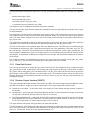
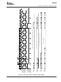
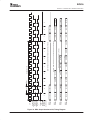
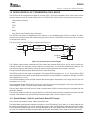
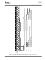
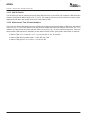
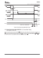
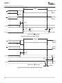
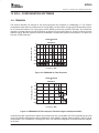
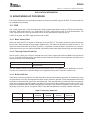
16.2 Dual Strobe, Edge Mode(WRMODE = 0), Control Bus Timing
(See Figures 27 and 28)
In this mode, an external processor (a microprocessor, computer, or DSP chip) can write into a register by setting
A[4..0] to the desired register address, setting RD high, selecting the chip by setting CE low, then strobing WR low.
The write cycle is active while both CE and WR are low. Data on the C[15..0] is registered into the chip on the rising
edge of WR. (see Figure 28)
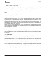
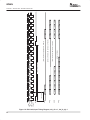
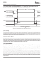
The external processor reads from a control register by setting A[0:4] to the desired address, select the chip with
the CE pin, and then set RD low. The chip then drives C[0:15] with the contents of the selected register. After the
processor has read the value from C[0:15] it should set RD and CE high (see Figure 27).
The C[0:15] pins are turned off (high impedance) whenever CE or RD are high or when WR is low.
CE
tREC
WR
tCSPW
RD
tsu(C)
A [4:0]
td(C)
t(CZ)
C [15:0]
READ CYCLE − NORMAL MODE
Figure 27. Dual Strobe Read Timing
54