1
www.ti.com
SLWS142J − JANUARY 2003 − REVISED AUGUST 2007
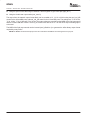
These devices have limited built-in ESD protection. The leads should be shorted together or the device placed in conductive foam during
storage or handling to prevent electrostatic damage to the MOS gates.
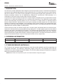
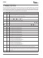
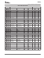
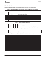
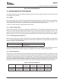
4 ABSOLUTE MAXIMUM RATINGS
over operating free-air temperature range unless otherwise noted(1)
GC5016
Pad ring supply voltage, VPAD
−0.3 V to 4 V
Core supply voltage, VCORE
−0.3 V to 2.3 V
Input voltage (undershoot and overshoot), VIN
−0.5 V to VPAD+0.5 V
Storage temperature, Tstg
−65°C to 150°C
Junction temperature, TJ
105°C
Lead soldering temperature (10 seconds)
300°C
ESD classification
Human body model
2 kV
Machine body model
200 V
Charged device model
500 V
Moisture sensitivity
Level 3
(1) Stresses beyond those listed under “absolute maximum ratings” may cause permanent damage to the device. These are stress ratings only, and
functional operation of the device at these or any other conditions beyond those indicated under “recommended operating conditions” is not
implied. Exposure to absolute-maximum-rated conditions for extended periods may affect device reliability.
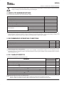
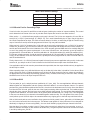
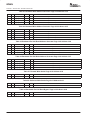
5 RECOMMENDED OPERATING CONDITIONS
Pad ring supply voltage, VPAD
MIN
MAX
3
3.6
UNITS
V
Core supply voltage, VCORE
1.6
2
V
Temperature ambient, no air flow, TA(1)
Junction temperature, TJ(2)
−40
85
_C
105
_C
(1) Chips specifications in the AC CHARACTERISTICS and DC CHARACTERISTICS tables are production tested at 100_C case temperature. QA
tests are performed at 85°C case temperature.
(2) Thermal management may be required for full rate operation (see the THERMAL CHARACTERISTICS table). The circuit is designed for junction
temperatures up to 125°C. Sustained operation at elevated temperatures reduces long-term reliability. Lifetime calculations based on maximum
junction temperature of 105°C.
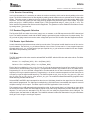
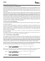
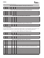
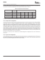
6 DC CHARACTERISTICS
−40°C to 85°C case temperature unless otherwise noted
PARAMETER
VIL
VIH
Voltage input low (1)
Voltage input high (1)
VOL
VOH
Voltage output low (IOL = 2 mA) (1)
Voltage output high (IOH = −2 mA) (1)
| IIN |
| IPU |
Leakage current (VIN = 0 V or VPAD), inputs or outputs in high-impedance state condition (1)
Pullup current (VIN = 0 V) ( TDI, TMS, TCK) (1)
ICCQ
CIN
Quiescent supply current, ICORE or IPAD(VIN=0 or VPAD, RST = TRST = 0) (1)
Data input capacitance (all inputs except CK) (2)
VPAD = 3 V to 3.6 V
MIN
TYP
MAX
0.8
2
UNIT
V
V
0.5
2.4
V
V
5
1
µA
35
µA
4
mA
4
pF
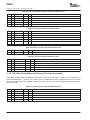
CCK
13
(1) Each part is tested with a 100°C case temperature for the given specification.
(2) Controlled by design and process and not directly tested.
NOTE: General: Voltages are measured at low speed. Output voltages are measured with the indicated current load.
General: Currents are measured at nominal voltages, high temperature (100_C for production test, 85_C for QA).
pF
Clock input capacitance (CK input) (2)
3