1
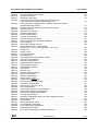
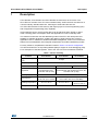
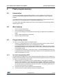
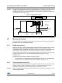
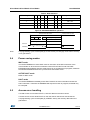
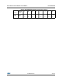
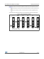
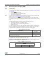
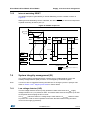
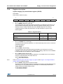
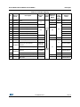
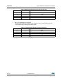
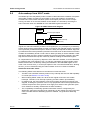
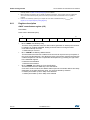
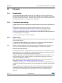
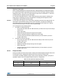
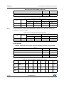
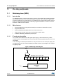
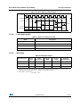
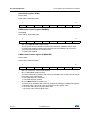
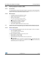
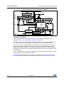
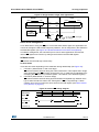
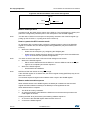
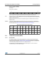
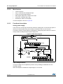
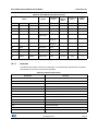
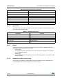
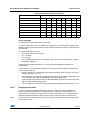
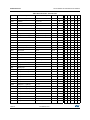
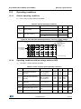
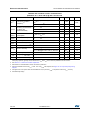
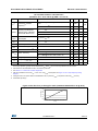
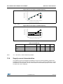
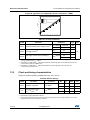
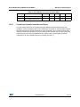
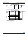
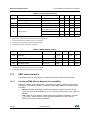
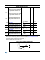
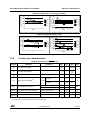
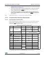
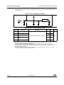
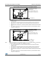
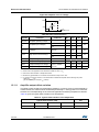
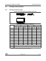
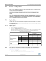
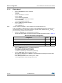
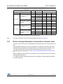
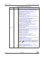
ST7LITE20F2 ST7LITE25F2 ST7LITE29F2
Electrical characteristics
Figure 82. Typical VOL vs. VDD (high-sink I/Os)
1.00
VOL vs VDD (HS) at lio=20mA
VOL vs VDD (HS) at lio=8mA
0.70
0.60
0.50
-45
0.40
0°C
25°C
0.30
90°C
130°C
0.20
0.10
0.00
2.4
3
0.90
0.80
0.70
-45
0.60
0°C
0.50
25°C
0.40
90°C
0.30
0.20
130°C
0.10
0.00
2.4
5
3
5
VDD (V)
VDD (V)
Figure 83. Typical VDD-VOH vs. VDD
1.80
1.10
VDD-VOH (V) at lio=-2mA
1.70
VDD-VOH at lio=-5mA
1.60
1.50
-45°C
0°C
25°C
90°C
130°C
1.40
1.30
1.20
1.10
1.00
1.00
0.90
-45°C
0.80
0°C
25°C
0.70
90°C
130°C
0.60
0.50
0.90
0.40
0.80
4
2.4
5
2.7
3
13.9
4
5
VDD (V)
VDD
Control pin characteristics
Table 82. Asynchronous RESET Pin(1)
Symbol
VIL
Parameter
Conditions
Min
Typ
Max
−
VSS 0.3
−
0.3xVDD
−
VDD +
0.3
−
2
−
IIO=+5mATA≤85°C
TA≥85°C
−
0.5
1.0
1.2
IIO=+2mATA≤85°C
TA≥85°C
−
0.2
0.4
0.5
VDD=5V
20
40
80
VDD=3V
40
70
120
−
30
−
μs
Input low level voltage
VIH
Input high level voltage
−
Vhys
Schmitt trigger voltage hysteresis(2)
−
VOL
RON
Output low level voltage(3)
Pull-up equivalent resistor(2)(4)
tw(RSTL)out Generated reset pulse duration
VDD=5V
Internal reset sources
0.7xVD
D
Unit
V
V
V
kΩ
th(RSTL)in
External reset pulse hold time(5)
−
20
−
−
μs
tg(RSTL)in
Filtered glitch duration
−
−
200
−
ns
1. TA = -40°C to 85°C, unless otherwise specified.
2. Data based on characterization results, not tested in production.
DocID8349 Rev 7
143/170
169