1
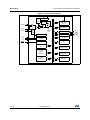
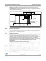
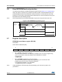
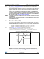
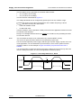
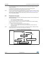
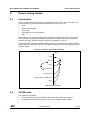
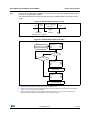
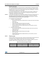
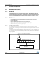
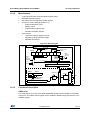
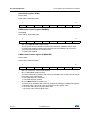
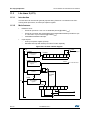
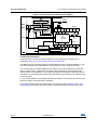
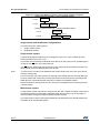
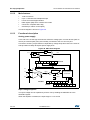
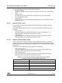
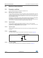
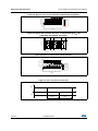
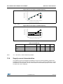
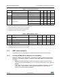
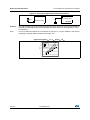
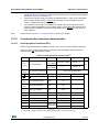
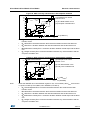
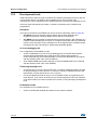
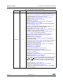
On-chip peripherals
ST7LITE20F2 ST7LITE25F2 ST7LITE29F2
PWM frequency and duty cycle
The four PWM signals have the same frequency (fPWM) which is controlled by the counter
period and the ATR register value.
fPWM = fCOUNTER / (4096 - ATR)
Following the above formula,
Note:
–
If fCOUNTER is 32 MHz, the maximum value of fPWM is 8 MHz (ATR register value =
4092), the minimum value is 8 KHz (ATR register value = 0)
–
If fCOUNTER is 4 Mhz, the maximum value of fPWM is 2 MHz (ATR register value =
4094),the minimum value is 1 KHz (ATR register value = 0).
The maximum value of ATR is 4094 because it must be lower than the DCR value which
must be 4095 in this case.
At reset, the counter starts counting from 0.
When a upcounter overflow occurs (OVF event), the preloaded Duty cycle values are
transferred to the Duty Cycle registers and the PWMx signals are set to a high level. When
the upcounter matches the DCRx value the PWMx signals are set to a low level. To obtain a
signal on a PWMx pin, the contents of the corresponding DCRx register must be greater
than the contents of the ATR register.
The polarity bits can be used to invert any of the four output signals. The inversion is
synchronized with the counter overflow if the TRAN bit in the TRANCR register is set (reset
value). See Figure 35.
Figure 35. PWM inversion diagram
inverter
PWMx
PWMx
pin
PWMxCSR register
OPx
DFF
TRAN
TRANCR register
counter
overflow
The maximum available resolution for the PWMx duty cycle is:
Resolution = 1 / (4096 – ATR)
Note:
76/170
To get the maximum resolution (1/4096), the ATR register must be 0. With this maximum
resolution, 0% and 100% can be obtained by changing the polarity.
DocID8349 Rev 7