1
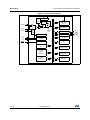
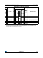
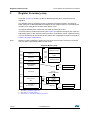
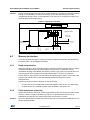
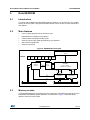
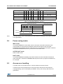
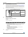
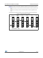
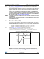
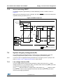
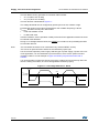
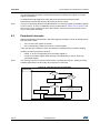
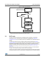
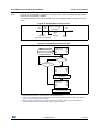
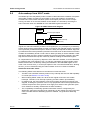
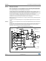
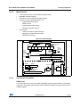
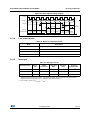
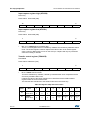
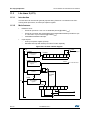
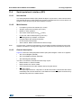
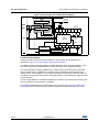
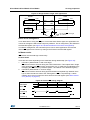
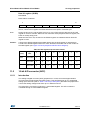
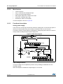
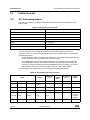
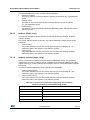
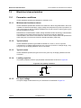
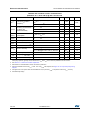
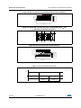
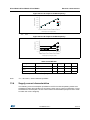
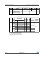
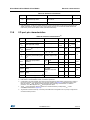
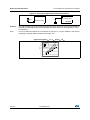
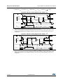
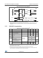
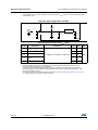
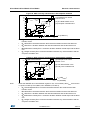
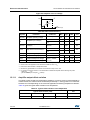
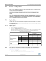
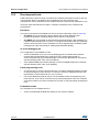
ST7LITE20F2 ST7LITE25F2 ST7LITE29F2
Supply, reset and clock management
7.5
Reset sequence manager (RSM)
7.5.1
Introduction
The reset sequence manager includes three RESET sources as shown in Figure 15: Reset
block diagram:
Note:
•
External RESET source pulse
•
Internal LVD RESET (low voltage detection)
•
Internal WATCHDOG RESET
A reset can also be triggered following the detection of an illegal opcode or prebyte code.
Refer to Section 12.2.1: Illegal opcode reset for further details.
These sources act on the RESET pin and it is always kept low during the delay phase.
The RESET service routine vector is fixed at addresses FFFEh-FFFFh in the ST7 memory
map.
The basic RESET sequence consists of 3 phases as shown in Figure 14:
•
Active Phase depending on the RESET source
•
256 or 4096 CPU clock cycle delay (see table below)
•
RESET vector fetch.
The 256 or 4096 CPU clock cycle delay allows the oscillator to stabilise and ensures that
recovery has taken place from the Reset state. The shorter or longer clock cycle delay is
automatically selected depending on the clock source chosen by option byte:
Table 8. CPU clock cycle delay
CPU clock
cycle delay
Clock source
Internal RC oscillator
256
External clock (connected to CLKIN pin)
256
External crystal/ceramic oscillator
(connected to OSC1/OSC2 pins)
4096
The RESET vector fetch phase duration is 2 clock cycles.
If the PLL is enabled by option byte, it outputs the clock after an additional delay of tSTARTUP
(see Figure 12: PLL output frequency timing diagram).
Figure 14. RESET sequence phases
RESET
Active phase
Internal reset
256 or 4096 clock cycles
DocID8349 Rev 7
Fetch
vector
39/170
169