1
On-chip peripherals
11.5.2
ST7LITE20F2 ST7LITE25F2 ST7LITE29F2
Main features
•
10-bit conversion
•
Up to 7 channels with multiplexed input
•
Linear successive approximation
•
Data register (DR) which contains the results
•
Conversion complete status flag
•
On/off bit (to reduce consumption)
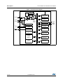
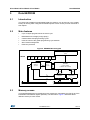
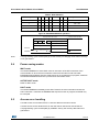
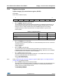
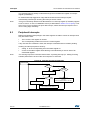
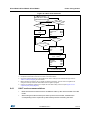
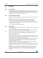
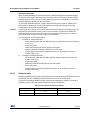
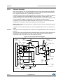
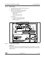
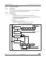
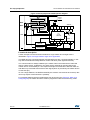
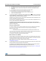
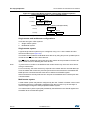
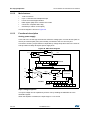
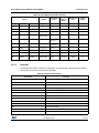
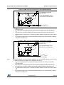
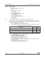
The block diagram is shown in Figure 49.
11.5.3
Functional description
Analog power supply
VDDA and VSSA are the high and low level reference voltage pins. In some devices (refer to
device pin out description) they are internally connected to the VDD and VSS pins.
Conversion accuracy may therefore be impacted by voltage drops and noise in the event of
heavily loaded or badly decoupled power supply lines.
Figure 49. ADC block diagram
fCPU
DIV 4
DIV 2
1
fADC
0
0
1
SLOW
bit
EOC SPEED ADON
0
0
CH2
CH1
ADCCSR
CH0
3
AIN0
HOLD CONTROL
AIN1
ANALOG
MUX
x 1 or
x8
RADC
ANALOG TO DIGITAL
CONVERTER
CADC
AINx
AMPSEL
bit
ADCDRH
D9
D8
ADCDRL
D7
D6
0
D5
0
D4
0
D3
D2
AMP
AMP
SLOW
CAL
SEL
D1
D0
Input voltage amplifier
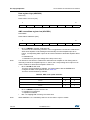
The input voltage can be amplified by a factor of 8 by enabling the AMPSEL bit in the
ADCDRL register.
When the amplifier is enabled, the input range is 0 V to VDD/8.
104/170
DocID8349 Rev 7