1
LMH6522
www.ti.com
SNOSB53D – JULY 2011 – REVISED MARCH 2013
LMH6522 High Performance Quad DVGA
Check for Samples: LMH6522
•
OIP3: 49dBm @ 200MHz
Noise Figure: 8.5dB
Voltage Gain: 26dB
1dB Gain Steps
−3dB Bandwidth of 1400 MHz
Gain Step Accuracy: 0.2 dB
Disable Function for Each Channel
Parallel and Serial Gain Control
Low Power Mode for Power Management
Flexibility
Small Footprint WQFN Package
APPLICATIONS
•
•
•
•
Cellular Base Stations
Wideband and Narrowband IF Sampling
Receivers
Wideband Direct Conversion
ADC Driver
DESCRIPTION
The LMH6522 contains four, high performance,
digitally controlled variable gain amplifiers (DVGA). It
has been designed for use in narrowband and
broadband IF sampling applications. Typically, the
LMH6522 drives a high performance ADC in a broad
range of mixed signal and digital communication
applications such as mobile radio and cellular base
stations where automatic gain control (AGC) is
required to increase system dynamic range.
The LMH6522 digitally controlled attenuator provides
precise 1dB gain steps over a 31dB range. The digital
attenuator can be controlled by either a SPI™ Serial
bus or a high speed parallel bus.
The output amplifier has a differential output, allowing
large signal swings on a single 5V supply. The low
impedance output provides maximum flexibility when
driving a wide range filter designs or analog to digital
converters. For applications which have very large
changes in signal level LMH6522 can support up to
62dB of gain range by cascading channels.
The LMH6522 operates over the industrial
temperature range of −40°C to +85°C. The LMH6522
is available in a 54-Pin, thermally enhanced, WQFN
package.
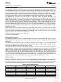
Performance Curve
60
35
50
30
40
25
30
20
20
f = 200 MHz
15
10
VOUT= 2VPPD
@ filter input
10
0
POWER GAIN (dB)
•
•
•
•
•
•
•
•
•
23
Each channel of LMH6522 has an independent,
digitally controlled attenuator and a high linearity,
differential output, amplifier. All circuitry has been
optimized for low distortion and maximum system
design flexibility. Power consumption is managed by
a three-state enable pin. Individual channels can be
disabled or placed into a Low Power Mode or a
higher performance, High Power Mode.
OIP3 (dBm)
FEATURES
1
5
50
100
150
200
250
300
FILTER INPUT RESISTANCE ( )
Figure 1. OIP3 vs Filter Input Resistance
1
2
3
Please be aware that an important notice concerning availability, standard warranty, and use in critical applications of
Texas Instruments semiconductor products and disclaimers thereto appears at the end of this data sheet.
SPI is a trademark of Motorola, Inc..
All other trademarks are the property of their respective owners.
PRODUCTION DATA information is current as of publication date.
Products conform to specifications per the terms of the Texas
Instruments standard warranty. Production processing does not
necessarily include testing of all parameters.
Copyright © 2011–2013, Texas Instruments Incorporated
LMH6522
SNOSB53D – JULY 2011 – REVISED MARCH 2013
www.ti.com
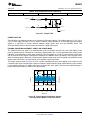
Block Diagram
+5V
Attenuator
INA+
OUTA+
26 dB
INA-
OUTA-
0 dB to 31 dB
Attenuator
INB+
OUTB+
26 dB
INB-
ATTEN_A
5
5
EN_A
4
SPI
ATTEN_D
OUTB-
0 dB to 31 dB
5
Digital
Control,
(Serial
or
Parallel)
EN_B
MODE
5
EN_D
INC+
ATTEN_B
ATTEN_C
EN_C
Attenuator
OUTC+
26 dB
INC-
IND+
OUTC-
0 dB to 31 dB
Attenuator
OUTD+
26 dB
IND-
0 dB to 31 dB
OUTD-
GND
These devices have limited built-in ESD protection. The leads should be shorted together or the device placed in conductive foam
during storage or handling to prevent electrostatic damage to the MOS gates.
2
Submit Documentation Feedback
Copyright © 2011–2013, Texas Instruments Incorporated
Product Folder Links: LMH6522
LMH6522
www.ti.com
SNOSB53D – JULY 2011 – REVISED MARCH 2013
Absolute Maximum Ratings (1) (2)
ESD Tolerance
(3)
Human Body Model
2 kV
Machine Model
200V
Charged Device Model
750V
−0.6V to 5.5V
Positive Supply Voltage (Pin 3)
Differential Voltage between Any Two Grounds
<200 mV
Analog Input Voltage Range
−0.6V to 5.5V
Digital Input Voltage Range
−0.6V to 5.5V
Output Short Circuit Duration
(one pin to ground)
Infinite
Junction Temperature
+150°C
−65°C to +150°C
Storage Temperature Range
Soldering Information
Infrared or Convection (30 sec)
(1)
(2)
(3)
260°C
Absolute Maximum Ratings indicate limits beyond which damage to the device may occur. Operating Ratings indicate conditions for
which the device is intended to be functional, but specific performance is not ensured. For ensured specifications, see the Electrical
Characteristics tables.
If Military/Aerospace specified devices are required, please contact the TI Sales Office/Distributors for availability and specifications.
Human Body Model, applicable std. MIL-STD-883, Method 3015.7. Machine Model, applicable std. JESD22-A115-A (ESD MM std. of
JEDEC)Field-Induced Charge-Device Model, applicable std. JESD22-C101-C (ESD FICDM std. of JEDEC).
Operating Ratings (1)
Supply Voltage (Pin 3)
4.75V to 5.25V
Differential Voltage Between Any Two Grounds
<10 mV
Analog Input Voltage Range,
AC Coupled
Temperature Range
(1)
(2)
0V to V+
(2)
−40°C to +85°C
Absolute Maximum Ratings indicate limits beyond which damage to the device may occur. Operating Ratings indicate conditions for
which the device is intended to be functional, but specific performance is not ensured. For ensured specifications, see the Electrical
Characteristics tables.
The maximum power dissipation is a function of TJ(MAX), θJA. The maximum allowable power dissipation at any ambient temperature is
PD = (TJ(MAX) – TA)/ θJA. All numbers apply for packages soldered directly onto a PC Board.
Package Thermal Resistance
(1)
54pin WQFN
(1)
(θJA)
(θJC)
23°C/W
4.7°C/W
Junction to ambient (θJA) thermal resistance measured on JEDEC 4 layer board. Junction to case (θJC) thermal resistance measured at
exposed thermal pad; package is not mounted to any PCB.
Submit Documentation Feedback
Copyright © 2011–2013, Texas Instruments Incorporated
Product Folder Links: LMH6522
3
LMH6522
SNOSB53D – JULY 2011 – REVISED MARCH 2013
www.ti.com
5V Electrical Characteristics (1) (2) (3)
The following specifications apply for single supply with V+ = 5V, Maximum Gain (0 Attenuation), RL = 200Ω, VOUT = 4VPPD,
fin = 200 MHz, High Power Mode, Boldface limits apply at temperature extremes.
Symbol
Parameter
Min
Conditions
(4)
Typ
(5)
Max
(4)
Units
Dynamic Performance
−3dB Bandwidth
VOUT= 2 VPPD
1.4
GHz
Output Noise Voltage
Source = 100Ω
30
nV/√Hz
NF
Noise Figure
Source = 100Ω
8.5
dB
OIP3
Output Third Order Intercept Point
f = 100 MHz, VOUT = 4 dBm per tone
53
dBm
Output Third Order Intercept Point
f = 200 MHz, VOUT = 4 dBm per tone
49
3dBBW
OIP2
Output Second Order Intercept Point POUT= 4 dBm per Tone, f1 =101 MHz,
f2=203 MHz
78
dBm
IMD3
Third Order Intermodulation
Products
f = 100 MHz, VOUT = 4 dBm per tone
−98
dBc
Third Order Intermodulation
Products
f = 200 MHz, VOUT = 4 dBm per tone
−90
P1dB
1dB Compression Point
17
dBm
HD2
Second Order Harmonic Distortion
f = 100 MHz, VOUT =2 VPPD
−88
dBc
HD2
Second Order Harmonic Distortion
f = 200 MHz, VOUT =2 VPPD
−78
dBc
HD3
Third Order Harmonic Distortion
f = 100 MHz, VOUT =2 VPPD
−99
dBc
HD3
Third Order Harmonic Distortion
f = 200 MHz, VOUT =2 VPPD
−75
dBc
CMRR
Common Mode Rejection
Pin = −15 dBm
−35
dBc
RIN
Input Resistance
Differential, Measured at DC
97
Ω
VICM
Input Common Mode Voltage
Self Biased
2.5
V
Maximum Input Voltage Swing
Volts peak to peak, differential
5.5
VPPD
Maximum DIfferential Output
Voltage Swing
Differential, f < 10MHz
10
VPPD
ROUT
Output Resistance
Differential, Measured at DC
20
Ω
XTLK
Channel to Channel Crosstalk
Maximum Gain, f=200MHz
−65
dBc
Analog I/O
Gain Parameters
Maximum Voltage Gain
Attenuation code 00000
25.74
dB
Minimum Gain
Attenuation code 11111
−4.3
dB
Gain Steps
32
Gain Step Size
1.0
dB
Channel Matching
Gain error between channels
±0.15
dB
Gain Step Error
Any two adjacent steps over entire range
±0.5
dB
Gain Step Error
Any two adjacent steps, 0 dB attenuation
to 23 dB attenuation
±0.1
dB
Gain Step Phase Shift
Any two adjacent steps over entire range
±3
Degrees
Gain Step Phase Shift
Any two adjacent steps, 0dB attenuation
to 23 dB attenuation
±2
20
ns
Settled to 90% level
200
ns
Gain Step Switching Time
Enable/ Disable Time
(1)
(2)
(3)
(4)
(5)
4
Degrees
Electrical Table values apply only for factory testing conditions at the temperature indicated. No specification of parametric performance
is indicated in the electrical tables under conditions different than those tested
Negative input current implies current flowing out of the device.
Drift determined by dividing the change in parameter at temperature extremes by the total temperature change.
Limits are 100% production tested at 25°C. Limits over the operating temperature range are specified through correlation using
Statistical Quality Control (SQC) methods.
Typical values represent the most likely parametric norm as determined at the time of characterization. Actual typical values may vary
over time and will also depend on the application and configuration. The typical values are not tested and are not ensured on shipped
production material.
Submit Documentation Feedback
Copyright © 2011–2013, Texas Instruments Incorporated
Product Folder Links: LMH6522
LMH6522
www.ti.com
SNOSB53D – JULY 2011 – REVISED MARCH 2013
5V Electrical Characteristics(1)(2)(3) (continued)
The following specifications apply for single supply with V+ = 5V, Maximum Gain (0 Attenuation), RL = 200Ω, VOUT = 4VPPD,
fin = 200 MHz, High Power Mode, Boldface limits apply at temperature extremes.
Symbol
Parameter
Conditions
Min
(4)
Typ
(5)
Max
(4)
Units
mA
Power Requirements
ICC
Supply Current
465
485
P
Power
2.3
2.43
IBIAS
Output Pin Bias Current
ICC
Disabled Supply Current
External inductor, no load, VOUT< 200 mV
W
36
mA
74
mA
All Digital Inputs Except Enables
Logic Compatibility
TTL, 2.5V CMOS, 3.3V CMOS, 5V CMOS
VIL
Logic Input Low Voltage
0
0.4
VIH
Logic Input High Voltage
2.0
5.0
V
IIH
Logic Input High Input Current
Digital Input Voltage = 2.0V
−9
μA
IIL
Logic Input Low Input Current
Digital Input Voltage = 0.4V
−47
μA
VIL
Logic Input Low Voltage
Amplifier disabled
0
0.4
V
VIM
Logic Input Mid Level
Amplifier Low Power Mode
0.6
1.9
V
VIH
Logic Input High Level
Amplifier High Power Mode
2.2
5
V
VSB
Enable Pin Self Bias Voltage
No external load
1.37
V
IIL
Input Bias Current, Logic Low
Digital input voltage = 0.2V
−200
µA
IIM
Input Bias Current, Logic Mid
Digital input voltage = 1.5V
28
µA
IIH
Input Bias Current, Logic High
Digital input voltage = 3.0V
500
µA
V
Enable Pins
Parallel Mode Timing
tGS
Setup Time
3
ns
tGH
Hold Time
3
ns
Serial Mode
fCLK
SPI Clock Frequency
50% duty cycle, ATE tested @ 20MHz
20
50
MHz
Low Power Mode
(Enable pins are self biased)
ICC
Total Supply Current
all four channels in low power mode
370
398
IBIAS
Output Pin Bias Current
External Inductor, No Load, VOUT< 200mV
26
ICC
Disabled Supply Current
Enable Pin < 0.4V
74
mA
OIP3
Output Intermodulation Intercept
Point
f = 200 MHz, V OUT = 4 dBm per tone
44
dBm
P1dB
1dB Compression Point
16
dBm
HD2
Second Order Harmonic Distortion
f = 100 MHz, VOUT =2 VPPD
−90
dBc
HD2
Second Order Harmonic Distortion
f = 200 MHz,VOUT = 2 VPPD
−79
dBc
HD3
Third Order Harmonic Distortion
f = 100 MHz, VOUT = 2 VPPD
−91
dBc
HD3
Third Order Harmonic Distortion
f = 200 MHz, VOUT = 2 VPPD
−79
dBc
Submit Documentation Feedback
Copyright © 2011–2013, Texas Instruments Incorporated
Product Folder Links: LMH6522
mA
mA
5
LMH6522
SNOSB53D – JULY 2011 – REVISED MARCH 2013
www.ti.com
B0
B1
B2
B3
B4
A0
A1/CLK
A2/CSb
A3/SDI
54
53
52
51
50
49
48
47
46
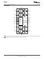
CONNECTION DIAGRAM
GND
1
45
A4/SDO
INA+
2
44
OUTA+
INA-
3
43
OUTA-
GND
4
42
+5VA
MODE
5
41
ENBA
GND
6
40
+5VB
INB+
7
39
OUTB+
INB-
8
38
OUTB-
GND
9
37
ENBB
GND
10
36
ENBC
INC+
11
35
OUTC+
INC-
12
34
OUTC-
GND
13
33
+5VC
GND
14
32
ENBD
GND
15
31
+5VD
IND+
16
30
OUTD+
IND-
17
29
OUTD-
GND
18
28
D4
Top View
10 mm x 5.5 mm x 0.8 mm
0.5 mm pitch
20
21
22
23
24
25
26
27
C2
C3
C4
D0
D1
D2
D3
19
C0
C1
GND
Figure 2. 54-Pin WQFN
Top View
PIN DESCRIPTIONS
Pin Number
Symbol
Pin Category
Description
2, 3
INA+, INA -
Analog Input
Differential inputs channel A
44, 43
OUTA+, OUTA-
Analog Output
Differential outputs Channel A
7, 8
INB+, INB -
Analog Input
Differential inputs channel B
39, 38
OUTB+, OUTB-
Analog Output
Differential outputs Channel B
11, 12
INC+, INC -
Analog Input
Differential inputs channel C
35, 34
OUTC+, OUTC-
Analog Output
Differential outputs Channel C
16, 17
IND+, IND -
Analog Input
Differential inputs channel D
30, 29
OUTD+, OUTD-
Analog Output
Differential outputs Channel D
1, 4, 6, 9, 10, 13, 14,
15, 18
GND
Ground
Ground pins. Connect to low impedance ground
plane. All pin voltages are specified with respect to
the voltage on these pins. The exposed thermal pad
is internally bonded to the ground pins.
31, 33, 40, 42
+5VD, +5VC, +5VB,
+5VA
Power
Power supply pins. Valid power supply range is
4.75V to 5.25V.
Thermal/ Ground
Thermal management/ Ground
Digital Input
0= Parallel Mode, 1 = Serial Mode
Analog I/O
Power
Exposed Center Pad
Digital Inputs
5
MODE
Parallel Mode Digital Pins, MODE = Logic Low
49, 48, 47, 46, 45
A0, A1, A2, A3, A4
Digital Input
Channel A attenuator control
41
ENBA
Digital Input
Channel A enable pin
54, 53, 52, 51, 50
B0, B1, B2, B3, B4
Digital Input
Channel B attenuator control
6
Submit Documentation Feedback
Copyright © 2011–2013, Texas Instruments Incorporated
Product Folder Links: LMH6522
LMH6522
www.ti.com
SNOSB53D – JULY 2011 – REVISED MARCH 2013
PIN DESCRIPTIONS (continued)
Pin Number
Symbol
Pin Category
Description
37
ENBB
Digital Input
Channel B enable pin: pin has three states: Low,
Mid, High
19, 20, 21, 22, 23
C0, C1, C2, C3, C4
Digital Input
Channel C attenuator control
36
ENBC
Digital Input
Channel C enable pin
24, 25, 26, 27, 28
D0, D1, D2, D3, D4
Digital Input
Channel D attenuator control
32
ENBD
Digital Input
Channel D enable pin
Serial Mode Digital Pins, MODE = Logic High
SPI™ Compatible
45
SDO
Digital Output- Open Collector
Serial Data Output (Requires external bias.)
46
SDI
Digital Input
Serial Data In
47
CSb
Digital Input
Chip Select
48
CLK
Digital Input
Clock
PIN LIST
Pin
Description
Pin
Description
1
GND
28
D4
2
INA+
29
OUTD−
3
INA−
30
OUTD+
4
GND
31
+5VD
5
MODE
32
ENBD
6
GND
33
+5VC
7
INB+
34
OUTC−
8
INB−
35
OUTC+
9
GND
36
ENBC
10
GND
37
ENBB
11
INC+
38
OUTB−
12
INC−
39
OUTB+
13
GND
40
+5VB
14
GND
41
ENBA
15
GND
42
+5VA
16
IND+
43
OUTA−
17
IND−
44
OUTA+
18
GND
45
A4 / SDO
19
C0
46
A3 / SDI
20
C1
47
A2 / CSb
21
C2
48
A1 / CLK
22
C3
49
A0
23
C4
50
B4
24
D0
51
B3
25
D1
52
B2
26
D2
53
B1
27
D3
54
BO
Submit Documentation Feedback
Copyright © 2011–2013, Texas Instruments Incorporated
Product Folder Links: LMH6522
7
LMH6522
SNOSB53D – JULY 2011 – REVISED MARCH 2013
www.ti.com
Typical Performance Characteristics
(TA = 25°C, V+ = 5V, RL = 200Ω, Maximum Gain, High Power, f= 200MHz; LMH6522 soldered onto LMH6522EVAL
evaluation board, Unless Specified).
Frequency Response, 2dB Steps
OIP3 vs Attenuation
52
30
POUT= 4dBm / Tone
25
48
OIP3 (dBm)
20
GAIN (dB)
15
10
5
0
44
High Power Mode
Low Power Mode
40
36
-5
32
-10
1
10
100
1000
0
10000
4
8 12 16 20 24
ATTENUATION (dB)
28
32
FREQUENCY (MHz)
Figure 3.
Figure 4.
OIP3 vs Output Power
OIP3 vs Load Resistance
52
55
50
44
OIP3 (dBm)
OIP3 (dBm)
48
High Power Mode
Low Power Mode
40
45
40
36
35
32
VOUT= 4VPPD
28
30
0
2
4
6
8
10
12
OUTPUT POWER, EACH TONE (dBm)
Figure 5.
0
100 200 300 400 500
LOAD RESISTANCE ( )
Figure 6.
OIP3 vs Frequency
OIP3 vs Supply Voltage
56
52
600
52
POUT=4dBm / Tone
OIP3 (dBm)
OIP3 (dBm)
48
48
44
44
40
40
36
32
100
8
High Power Mode
Low Power Mode
200
300
400
FREQUENCY (MHz)
Figure 7.
High Power Mode
Low Power Mode
36
500
Submit Documentation Feedback
4.50
4.75
5.00
5.25
SUPPLY VOLTAGE (V)
Figure 8.
5.50
Copyright © 2011–2013, Texas Instruments Incorporated
Product Folder Links: LMH6522
LMH6522
www.ti.com
SNOSB53D – JULY 2011 – REVISED MARCH 2013
Typical Performance Characteristics (continued)
(TA = 25°C, V+ = 5V, RL = 200Ω, Maximum Gain, High Power, f= 200MHz; LMH6522 soldered onto LMH6522EVAL
evaluation board, Unless Specified).
OIP3 vs Temperature
Supply Current vs Supply Voltage
56
SUPPLY CURRENT (mA)
550
OIP3 (dBm)
52
48
44
High Power Mode
Low Power Mode
40
High Power Mode
Low Power Mode
500
450
400
350
300
-45 -30 -15 0 15 30 45 60 75 90
TEMPERATURE (Degrees C)
Figure 9.
4.50
Supply Current vs Temperature
450
425
400
375
27.0
26.5
26.0
25.5
25.0
24.5
350
24.0
-45 -30 -15 0 15 30 45 60 75 90
TEMPERATURE (Degrees C)
Figure 11.
-45 -30 -15 0 15 30 45 60 75 90
TEMPERATURE (Degrees C)
Figure 12.
HD2 vs Frequency, High Power Mode
Ch A
Ch B
Ch C
Ch D
-30
HD3 vs Frequency, High Power Mode
-20
Ch A
Ch B
POUT=10dBm
-30
Ch C
Ch D
-40
POUT=10dBm
HD3 (dBc)
-40
HD2 (dB)
High Power Mode
Low Power Mode
27.5
475
-20
5.50
Maximum Gain vs Temperature
28.0
High Power Mode
Low Power Mode
MAXIMUM GAIN (dB)
SUPPLY CURRENT (mA)
500
4.75
5.00
5.25
SUPPLY VOLTAGE (V)
Figure 10.
-50
-60
-70
-50
-60
-70
-80
-80
-90
-90
-100
0
100
200
300
400
FREQUENCY (MHz)
Figure 13.
500
0
100
200
300
400
FREQUENCY (MHz)
Figure 14.
500
Submit Documentation Feedback
Copyright © 2011–2013, Texas Instruments Incorporated
Product Folder Links: LMH6522
9
LMH6522
SNOSB53D – JULY 2011 – REVISED MARCH 2013
www.ti.com
Typical Performance Characteristics (continued)
(TA = 25°C, V+ = 5V, RL = 200Ω, Maximum Gain, High Power, f= 200MHz; LMH6522 soldered onto LMH6522EVAL
evaluation board, Unless Specified).
HD2 vs Frequency, Low Power Mode
-30
Ch A
Ch B
POUT= 10dBm
Ch C
-40
Ch D
HD3 vs Frequency, Low Power Mode
-20
-30
-60
-70
-50
-60
-80
-70
-90
-80
-100
-90
0
100
200
300
400
FREQUENCY (MHz)
Figure 15.
500
0
100
200
300
400
FREQUENCY (MHz)
Figure 16.
HD2 vs Attenuation
-40
HD3 (dBc)
HD2 (dBc)
High Power Mode
Low Power Mode
-50
-60
POUT= 4dBm
-70
-60
-80
-90
-90
4
8 12 16 20 24
ATTENUATION (dB)
Figure 17.
28
POUT= 4dBm
-70
-80
0
32
0
4
HD2 vs Output Power
-20
8 12 16 20 24
ATTENUATION (dB)
Figure 18.
28
32
HD3 vs Output Power
-20
High Power Mode
Low Power Mode
-30
High Power Mode
Low Power Mode
-30
-40
HD3 (dBc)
-40
HD2 (dBc)
500
HD3 vs Attenuation
-40
High Power Mode
Low Power Mode
-50
-50
-60
-70
-50
-60
-70
-80
-80
-90
-90
-100
-100
-4
10
POUT=10dBm
-40
HD3 (dBc)
-50
HD2 (dBc)
Ch A
Ch B
Ch C
Ch D
0
4
8
12
16
OUTPUT POWER (dBm)
Figure 19.
20
Submit Documentation Feedback
-4
0
4
8
12
16
OUTPUT POWER (dBm)
Figure 20.
20
Copyright © 2011–2013, Texas Instruments Incorporated
Product Folder Links: LMH6522
LMH6522
www.ti.com
SNOSB53D – JULY 2011 – REVISED MARCH 2013
Typical Performance Characteristics (continued)
(TA = 25°C, V+ = 5V, RL = 200Ω, Maximum Gain, High Power, f= 200MHz; LMH6522 soldered onto LMH6522EVAL
evaluation board, Unless Specified).
Isolation, Adjacent Channels
-20
-40
IN A OUT C
IN A OUT D
IN B OUT D
IN C OUT A
IN D OUT A
IN D OUT B
-50
ISOLATION (dBc)
-30
ISOLATION (dBc)
Isolation, Non-Adjacent Channels
-40
IN A OUT B
IN B OUT A
IN B OUT C
IN C OUT B
IN C OUT D
IN D OUT C
-50
-60
-70
-80
-60
-70
-80
-90
-100
-90
-110
10
100
FREQUENCY (MHz)
Figure 21.
1000
10
2
1
0
2
1
0
-1
-1
-2
-2
10
A to B
A to C
A to D
3
GAIN MATCHING (dB)
GAIN MATCHING (dB)
4
A to B
A to C
A to D
3
100
FREQUENCY (MHz)
Figure 23.
10
1000
Gain Step Amplitude Error
1.0
PHASE ERROR (Degrees)
AMPLITUDE ERROR (dB)
0.4
0.2
0.0
-0.2
-0.4
2
0
-2
-4
-6
50 MHz
200 MHz
300 MHz
-8
-0.6
6
11
16
21
ATTENUATION (dB)
Figure 25.
1000
Gain Step Phase Error
0.6
1
100
FREQUENCY (MHz)
Figure 24.
4
50 MHz
200 MHz
300 MHz
0.8
1000
Channel Matching
Attenuation Code 10000
Channel Matching, Maximum Gain
4
100
FREQUENCY (MHz)
Figure 22.
26
31
1
6
11
16
21
ATTENUATION (dB)
Figure 26.
26
31
Submit Documentation Feedback
Copyright © 2011–2013, Texas Instruments Incorporated
Product Folder Links: LMH6522
11
LMH6522
SNOSB53D – JULY 2011 – REVISED MARCH 2013
www.ti.com
Typical Performance Characteristics (continued)
(TA = 25°C, V+ = 5V, RL = 200Ω, Maximum Gain, High Power, f= 200MHz; LMH6522 soldered onto LMH6522EVAL
evaluation board, Unless Specified).
Cumulative Amplitude Error
2.0
2
PHASE ERROR (Degrees)
1.5
AMPLITUDE ERROR (dB)
Cumulative Phase Error
4
50 MHz
200 MHz
300 MHz
1.0
0.5
0.0
-0.5
0
-2
-4
50 MHz
200 MHz
300 MHz
-6
-8
-10
-12
-14
-16
-1.0
6
11
16
21
ATTENUATION (dB)
Figure 27.
26
1
31
14
36
13
32
28
24
20
16
10
9
8
7
8 12 16 20 24
ATTENUATION (dB)
Figure 29.
28
32
0
Enable Timing, High Power
400
Enable Timing, Low Power
2
4
2
2
1
3
1
1
0
2
0
0
-1
1
-1
-1
0
-2
-2
0
100 200 300 400 500 600 700 800
TIME (ns)
Figure 31.
VOUT(V)
3
Output
Enable Pin
ENA PIN (V)
VOUT(V)
100
200
300
FREQUENCY (MHz)
Figure 30.
5
3
12
31
11
8
4
26
12
12
0
11
16
21
ATTENUATION (dB)
Figure 28.
Noise Figure vs Frequency
40
NOISE FIGURE (dB)
NOISE FIGURE (dB)
Noise Figure vs Attenuation
6
Output
Enable Pin
3
ENA PIN (V)
1
-2
0
Submit Documentation Feedback
100 200 300 400 500 600 700 800
TIME (ns)
Figure 32.
Copyright © 2011–2013, Texas Instruments Incorporated
Product Folder Links: LMH6522
LMH6522
www.ti.com
SNOSB53D – JULY 2011 – REVISED MARCH 2013
Typical Performance Characteristics (continued)
(TA = 25°C, V+ = 5V, RL = 200Ω, Maximum Gain, High Power, f= 200MHz; LMH6522 soldered onto LMH6522EVAL
evaluation board, Unless Specified).
Gain Step Timing, 8dB Step
5
3
2
4
2
4
1
3
1
3
0
2
0
2
-1
1
-1
1
0
-2
10
20
30 40 50 60
TIME (ns)
Figure 33.
70
VOUT(V)
80
0
0
10
Gain Step Timing, 4dB Step
30 40 50 60
TIME (ns)
Figure 34.
70
80
Gain Step Timing, 2dB Step
3
5
3
2
4
2
4
1
3
1
3
0
2
0
2
-1
1
-1
1
-2
0
-2
0
0
10
20
30 40 50 60
TIME (ns)
Figure 35.
70
VOUT(V)
A2 PIN (V)
80
0
10
Gain Step Timing, 1dB Step
3
5
Output
A1 Pin
Output
A2 Pin
VOUT(V)
20
20
30 40 50 60
TIME (ns)
Figure 36.
70
A1 PIN (V)
0
A4 PIN (V)
VOUT(V)
-2
5
Output
A3 Pin
Output
A4 Pin
A3 PIN (V)
Gain Step Timing, 16dB Step
3
80
CMRR vs Frequency
-10
5
Output
A0 Pin
Maximum Gain
16dB Attenuation
-20
2
4
3
0
2
-1
1
CMRR (dBc)
1
A0 PIN (V)
VOUT(V)
-30
-40
-50
-60
-70
-2
0
0
10
20
30 40 50 60
TIME (ns)
Figure 37.
70
-80
80
1
10
100
FREQUENCY (MHz)
Figure 38.
1000
Submit Documentation Feedback
Copyright © 2011–2013, Texas Instruments Incorporated
Product Folder Links: LMH6522
13
LMH6522
SNOSB53D – JULY 2011 – REVISED MARCH 2013
www.ti.com
Typical Performance Characteristics (continued)
(TA = 25°C, V+ = 5V, RL = 200Ω, Maximum Gain, High Power, f= 200MHz; LMH6522 soldered onto LMH6522EVAL
evaluation board, Unless Specified).
Input Impedance
R
jX
|Z|
INPUT IMPEDANCE ( )
250
Output Impedance
150
Z = R + jX
R
jX
|Z|
125
OUTPUT IMPEDANCE ( )
300
200
150
100
50
0
-50
100
75
50
25
0
-25
-100
-50
0
100
200
300
400
FREQUENCY (MHz)
Figure 39.
500
0
Power Sweep, High Power Mode
16
100
200
300
400
FREQUENCY (MHz)
Figure 40.
500
Power Sweep, Low Power Mode
20
100 MHz
200 MHz
300 MHz
OUTPUT POWER (dBm)
OUTPUT POWER (dBm)
20
12
8
4
0
100 MHz
200 MHz
300 MHz
16
12
8
4
0
-4
-4
-30
-25 -20 -15 -10
-5
INPUT POWER (dBm)
0
Figure 41.
14
Z = R +jX
-30
-25 -20 -15 -10
-5
INPUT POWER (dBm)
0
Figure 42.
Submit Documentation Feedback
Copyright © 2011–2013, Texas Instruments Incorporated
Product Folder Links: LMH6522
LMH6522
www.ti.com
SNOSB53D – JULY 2011 – REVISED MARCH 2013
APPLICATION INFORMATION
100:
FILTER
VCC
1 PH
0.01 PF
RF
40.2:
100:
0.01 PF
100:
FILTER
¼ LMH6522
ADC
40.2:
0.01 PF
0.01 PF
100:
1 PH
LO
5
GAIN 0-4
ENABLE
Figure 43. LMH6522 Typical Application
INTRODUCTION
The LMH6522 is a fully differential amplifier optimized for signal path applications up to 400 MHz. The LMH6522
has a 100Ω input and a low impedance output. The gain is digitally controlled over a 31 dB range from +26dB to
−5dB. The LMH6522 is optimized for accurate gain steps and minimal phase shift combined with low distortion
products. This makes the LMH6522 ideal for voltage amplification and an ideal analog to digital converter (ADC)
driver where high linearity is necessary.
+5V
Attenuator
INA+
OUTA+
26 dB
INA-
OUTA-
0 dB to 31 dB
Attenuator
INB+
OUTB+
26 dB
INB-
ATTEN_A
5
EN_A
4
SPI
ATTEN_D
OUTB-
0 dB to 31 dB
5
5
Digital
Control,
(Serial
or
Parallel)
EN_B
MODE
5
EN_D
INC+
ATTEN_B
ATTEN_C
EN_C
Attenuator
OUTC+
26 dB
INC-
IND+
OUTC-
0 dB to 31 dB
Attenuator
OUTD+
26 dB
IND-
0 dB to 31 dB
OUTD-
GND
Figure 44. LMH6522 Block Diagram
Submit Documentation Feedback
Copyright © 2011–2013, Texas Instruments Incorporated
Product Folder Links: LMH6522
15
LMH6522
SNOSB53D – JULY 2011 – REVISED MARCH 2013
www.ti.com
BASIC CONNECTIONS
A voltage between 4.75 V and 5.25 V should be applied to the supply pin labeled +5V. Each supply pin should
be decoupled with a low inductance, surface-mount ceramic capacitor of 0.01uF as close to the device as
possible. Additional bypass capacitors of 0.1uF and 1nF are optional, but would provide bypassing over a wider
frequency range.
The outputs of the LMH6522 need to be biased to ground using inductors and output coupling capacitors of
0.01uF are recommended. The input pins are self biased to 2.5V and should be ac-coupled with 0.01uF
capacitors as well. The output bias inductors and ac-coupling capacitors are the main limitations for operating at
low frequencies. Larger values of inductance on the bias inductors and larger values of capacitance on the
coupling capacitors will give more low frequency range. Using bias inductors over 1 uH, however, may
compromise high frequency response due to unwanted parasitic loading on the amplifier output pins.
Each channel of the LMH6522 consists of a digital step attenuator followed by a low distortion 26 dB fixed gain
amplifier and a low impedance output stage. The attenuation is digitally controlled over a 31 dB range from 0dB
to 31dB. The LMH6522 has a 100Ω differential input impedance and a low, 20Ω, output impedance.
Each channel of the LMH6522 has an enable pin. Grounding the enable pin will put the channel in a power
saving shutdown mode. Additionally, there are two “on” states which gives the option of two power modes. High
Power Mode is selected by biasing the enable pins at 2.0 V or higher. The LMH6522 enable pins will self bias to
the Low Power State, alternatively supplying a voltage between 0.6V and 1.8V will place the channel in Low
Power Mode. If connected to a TRI-STATE buffer the LMH6522 enable pins will be in shutdown for a logic 0
output, in High Power Mode for a logic 1 state and they will self bias to Low Power Mode for the high impedance
state.
+5V
0.01 PF
+
SOURCE
50:
LOAD
0.01 PF
OUT+
IN+
0.01 PF
40.2:
¼
LMH6522
AC
100:
OUT-
50:
0.01 PF
IN 40.2:
5
1 PH
0.01 PF
1 PH
A0 ± A4
Figure 45. LMH6522 Basic Connections Schematic
INPUT CHARACTERISTICS
The LMH6522 input impedance is set by internal resistors to a nominal 100Ω. Process variations will result in a
range of values. At higher frequencies parasitic reactances will start to impact the impedance. This characteristic
will also depend on board layout and should be verified on the customer’s system board.
At maximum gain the digital attenuator is set to 0 dB and the input signal will be much smaller than the output. At
minimum gain the output is 5 dB or more smaller than the input. In this configuration the input signal will begin to
clip against the ESD protection diodes before the output reaches maximum swing limits. The input signal cannot
swing more than 0.5V below the negative supply voltage (normally 0V) nor should it exceed the positive supply
voltage. The input signal will clip and cause severe distortion if it is too large. Because the input stage self biases
to approximately mid rail the supply voltage will impose the limit for input voltage swing.
At higher frequencies the LMH6522 input impedance is not purely resistive. In Figure 46 a circuit is shown that
matches the amplifier input impedance with a source that is 100Ω. This would be the case when connecting the
LMH6522 directly to a mixer. For an easy way to calculate the L and C circuit values there are several options for
online tools or down-loadable programs. The following tool might be helpful.
16
Submit Documentation Feedback
Copyright © 2011–2013, Texas Instruments Incorporated
Product Folder Links: LMH6522
LMH6522
www.ti.com
SNOSB53D – JULY 2011 – REVISED MARCH 2013
Excel can also be used for simple circuits; however, the “Analysis ToolPak” add-in must be installed to calculate
complex numbers.
http://www.circuitsage.com/matching/matcher2.html
SOURCE IMPEDANCE = 100:
f = 200 MHz
ZAMP = (130 + j10):
ZIN = (97.8-j1.5):
5V
L1
LMH6522
ZAMP
ZIN
C1
L2
L1, L2 = 22 nH
C1 = 4 pF
5
GAIN 0-4
Figure 46. Differential LC Conversion Circuit
OUTPUT CHARACTERISTICS
The LMH6522 has a low impedance output very similar to a traditional Op-amp output. This means that a wide
range of loads can be driven with good performance. Matching load impedance for proper termination of filters is
as easy as inserting the proper value of resistor between the filter and the amplifier. This flexibility makes system
design and gain calculations very easy.
By using a differential output stage the LMH6522 can achieve very large voltage swings on a single 5V supply.
This is illustrated in Figure 47. This figure shows how a voltage swing of 5VPPD is realized while only swinging 2.5
VPP on each output. The LMH6522 can swing up to 10 VPPD which is sufficient to drive most ADCs to full scale
while using a matched impedance anti alias filter between the amplifier and the ADC. The LMH6522 has been
designed for AC coupled applications and has been optimized for operation above 5 MHz.
2.5
(OUT+) - (OUT-)
2.0
1.5
VOUT (V)
1.0
OUT+
0.5
1.25 VP
0.0
-0.5
OUT-
-1.0
2.5 VPP
-1.5
-2.0
-2.5
0
5 VPPD (DIFFERENTIAL)
45
90
135 180 225 270 315 360
PHASE (Degrees)
Figure 47. Differential Output Voltage
Like most closed loop amplifiers the LMH6522 output stage can be sensitive to capacitive loading. To help with
board layout and to help minimize sensitivity to bias inductor capacitance the LMH5522 output lines have internal
10Ω resistors. These resistors should be taken into account when choosing matching resistor values. This is
shown in Figure 45 as using 40.2 Ω resistors instead of 50 Ω resistors to match the 100 Ω differential load. Best
practise is to place the external termination resistors as close to the DVGA output pins as possible. Due to
reactive components between the DVGA output and the filter input it may be desirable to use even smaller value
resistors than a simple calculation would indicate. For instance, at 200 MHz resistors of 30 Ohms provide slightly
better OIP3 performance on the LMH6522EVAL evaluation board and may also provide a better match to the
filter input.
Submit Documentation Feedback
Copyright © 2011–2013, Texas Instruments Incorporated
Product Folder Links: LMH6522
17
LMH6522
SNOSB53D – JULY 2011 – REVISED MARCH 2013
www.ti.com
The LMH6522 output pins require a DC path to ground. On the evaluation board, inductors are installed to
provide proper output biasing. The bias current is approximately 36mA per output pin. The resistance of the
output bias inductors will raise the output common mode slightly. An inductor with low resistance will keep the
output bias voltage close to zero, so the DC resistance of the inductor chosen will be important. It is also
important to make sure that the inductor can handle the 36mA of bias current.
In addition to the DC current in the inductor there will be some AC current as well. With large inductors and high
operating frequencies the inductor will present a very high impedance and will have minimal AC current. If the
inductor is chosen to have a smaller value, or if the operating frequency is very low there could be enough AC
current flowing in the inductor to become significant. The total current should not exceed the inductor current
rating.
Another reason to choose low resistance bias inductors is that due to the nature of the LMH6522 output stage,
the output offset voltage is determined by the output bias components. The output stage has an offset current
that is typically 3mA and this offset current, multiplied by the resistance of the output bias inductors will
determine the output offset voltage.
The ability of the LMH6522 to drive low impedance loads while maintaining excellent OIP3 performance creates
an opportunity to greatly increase power gain and drive low impedance filters. Figure 48 shows the OIP3
performance of the LMH6522 over a range of filter impedances. Also on the same graph is the power gain
realized by changing load impedance. The power gain reflects the 6dB of loss caused by the termination
resistors necessary to match the amplifier output impedance to the filter characteristic impedance. The graphs
shows the ability of the LMH6522 to drive a constant voltage to an ADC input through various filter impedances
with very little change in OIP3 performance. This gives the system designer much needed flexibility in filter
design.
55
40
OIP3 High Power Mode
35
OIP3 Low Power Mode
OIP3 (dBm)
45
30
40
25
Power Gain @ Load
35
30
20
POWER GAIN (dB)
50
15
VOUT= 4VPPD
f = 200 MHz
25
10
50
100
150
200
250
300
FILTER INPUT RESISTANCE ( )
Figure 48. OIP3 and Power Gain vs Filter Impedance
OIP3 and Gain Measured at Amplifier Output, Filter Back Terminated
Printed circuit board (PCB) design is critical to high frequency performance. In order to ensure output stability the
load matching resistors should be placed as close to the amplifier output pins as possible. This allows the
matching resistors to mask the board parasitics from the amplifier output circuit. An example of this is shown in
Figure 49. If the FIilter is a bandpass filter with no DC path the 0.01µF coupling capacitors can be eliminated.
The LMH6522EVAL evaluation board is available to serve a guide for system board layout.
1P
RT
+
0.01P
FILTER
+IN
RT
¼ LMH6522
RT
.
1P
RT
VRM ADC16DV160
-IN
0.01P
Figure 49. Output Configuration
18
Submit Documentation Feedback
Copyright © 2011–2013, Texas Instruments Incorporated
Product Folder Links: LMH6522
LMH6522
www.ti.com
SNOSB53D – JULY 2011 – REVISED MARCH 2013
CASCADE OPERATION
VCC
VCC
1 PH
1 PH
0.01 PF
0.01 PF
100:
VIN
¼ LMH6522
40.2:
100:
0.01 PF
0.01 PF
¼ LMH6522
VOUT
40.2:
0.01 PF
0.01 PF
1 PH
1 PH
Figure 50. Schematic for Cascaded Amplifiers
With four amplifiers in one package the LMH6522 is ideally configured for cascaded operation. By using two
amplifiers in series additional gain range can be achieved. The schematic in Figure 50 shows one way to
connect two stages of the LMH6522. The resultant frequency response is shown below in Figure 51. When using
the LMH6522 amplifiers in a cascade configuration it is important to keep the signal level within reasonable limits
at all nodes of the signal path. With over 40dB of total gain it is possible to amplify signals to clipping levels if the
gain is not set correctly.
50
GAIN @ LOAD (dB)
40
30
20
10
0
-10
-20
1
10
100
FREQUENCY (MHz)
1000
Figure 51. Frequency Response of Cascaded Amplifiers
DIGITAL CONTROL
The LMH6522 will support two modes of control, parallel mode and serial mode (SPI compatible). Parallel mode
is fastest and requires the most board space for logic line routing. Serial mode is compatible with existing SPI
compatible systems.
The LMH6522 has gain settings covering a range of 31 dB. To avoid undesirable signal transients the LMH6522
should not be powered on with large inputs signals present. Careful planning of system power on sequencing is
especially important to avoid damage to ADC inputs.
The LMH6522 was designed to interface with 2.5V to 5V CMOS logic circuits. If operation with 5V logic is
required care should be taken to avoid signal transients exceeding the DVGA supply voltage. Long, unterminated
digital signal traces are particularly susceptible to these transients. Signal voltages on the logic pins that exceed
the device power supply voltage may trigger ESD protection circuits and cause unreliable operation.
Some pins on the LMH6522 have different functions depending on the digital control mode. These functions will
be described in the sections to follow.
Submit Documentation Feedback
Copyright © 2011–2013, Texas Instruments Incorporated
Product Folder Links: LMH6522
19
LMH6522
SNOSB53D – JULY 2011 – REVISED MARCH 2013
www.ti.com
Table 1. Pins with Dual Functions (1)
Pin
MODE = 0
MODE = 1
45
A4
SDO*
46
A3
SDI
47
A2
CSb
48
A1
CLK
(1)
Pin 45 requires external bias. See Serial Mode Section for Details.
PARALLEL INTERFACE
Parallel mode offers the fastest gain update capability with the drawback of requiring the most board space
dedicated to control lines. When designing a system that requires very fast gain changes parallel mode is the
best selection. To place the LMH6522 into parallel mode the MODE pin (pin 5) is set to the logical zero state.
Alternately the MODE pin can be connected directly to ground.
The attenuator control pins are internally biased to logic high state with weak pull up resistors. The MODE pin
has a weak internal resistor to ground. The enable pins bias to a mid logic state which is the Low Power Mode.
The LMH6522 has a 5-bit gain control bus. Data from the gain control pins is immediately sent to the gain circuit
(i.e. gain is changed immediately). To minimize gain change glitches all gain pins should change at the same
time. In order to achieve the very fast gain step switching time the internal gain change circuit is very fast. Gain
glitches could result from timing skew between the gain set bits. This is especially the case when a small gain
change requires a change in state of three or more gain control pins. If necessary the DVGA could be put into a
disabled state while the gain pins are reconfigured and then brought active when they have settled.
ENA , ENB, ENC and END pins are provided to reduce power consumption by disabling the highest power
portions of the LMH6522. The gain register will preserve the last active gain setting during the disabled state.
These pins have three logic states and will float to the middle or low power, enabled state if left floating. When
grounded the EN pins will disable the associated channel and when biased to the highest logic level the
associated channel will be in the high power, enabled state. See the Typical Performance Characteristics section
for disable and enable timing information.
LMH6522
CONTROL LOGIC
4
pd
ga[4:0]
gb[4:0]
en[a:d]*
5
5
ga[4:0]
gb[4:0]
5
gc[4:0]
gd[4:0]
gc[4:0]
5
gd[4:0]
*Enable pins are tri state buffer compatible.
Figure 52. Parallel Mode Connection
SPI™ COMPATIBLE SERIAL INTERFACE
Serial interface allows a great deal of flexibility in gain programming and reduced board complexity. Using only 4
wires for both channels allows for significant board space savings. The trade off for this reduced board
complexity is slower response time in gain state changes. For systems where gain is changed only infrequently
or where only slow gain changes are required serial mode is the best choice. To place the LMH6522 into serial
mode the MODE pin (Pin 5) should be put into the logic high state. Alternatively the MODE pin an be connected
directly to the 5V supply bus.
The LMH6522 serial interface is a generic 4-wire synchronous interface that is compatible with SPI type
interfaces that are used on many microcontrollers and DSP controllers. In this configuration the pins function as
shown in the pin description table. The SPI interface uses the following signals: clock input (CLK), serial data in
(SDI), serial data out (SDO), and serial chip select (CSb). The chip select pin is active low.
The enable pins are inactive in the serial mode. These pins can be left disconnected for serial mode.
20
Submit Documentation Feedback
Copyright © 2011–2013, Texas Instruments Incorporated
Product Folder Links: LMH6522
LMH6522
www.ti.com
SNOSB53D – JULY 2011 – REVISED MARCH 2013
The CLK pin is the serial clock pin. It is used to register the input data that is presented on the SDI pin on the
rising edge; and to source the output data on the SDO pin on the falling edge. User may disable clock and hold it
in the low state, as long as the clock pulse-width minimum specification is not violated when the clock is enabled
or disabled.
The CSb pin is the chip select pin. The b indicates that this pin is actually a “NOT chip select” since the chip is
selected in the logic low state. Each assertion starts a new register access - i.e., the SDATA field protocol is
required. The user is required to deassert this signal after the 16th clock. If the CSb pin is deasserted before the
16th clock, no address or data write will occur. The rising edge captures the address just shifted-in and, in the
case of a write operation, writes the addressed register. There is a minimum pulse-width requirement for the
deasserted pulse - which is specified in the Electrical Specifications section.
The SDI pin is the input pin for the serial data. It must observe setup / hold requirements with respect to the
SCLK. Each cycle is 16-bits long
The SDO pin is the data output pin. This output is normally at a high impedance state, and is driven only when
CSb is asserted. Upon CSb assertion, contents of the register addressed during the first byte are shifted out with
the second 8 SCLK falling edges. Upon power-up, the default register address is 00h. The SDO pin requires
external bias for clock speeds over 1MHz. See Figure 54 for details on sizing the external bias resistor. Because
the SDO pin is a high impedance pin, the board capacitance present at the pin will restrict data out speed that
can be achieved. For a RC limited circuit the frequency is ~ 1/ (2*Pi*RC). As shown in the figure resistor values
of 300 to 2000 Ohms are recommended.
Each serial interface access cycle is exactly 16 bits long as shown in Figure 53. Each signal's function is
described below. the read timing is shown in Figure 55, while the write timing is shown in Figure 56.
1
2
3
4
5
6
7
8
9
10
11
12
13
14
15
16
D2
D1
D0
(LSB)
D2
D1
17
SCLK
CSb
COMMAND FIELD
SDI
C7
C6
C5
C4
R/Wb
0
0
0
Reserved (3-bits)
DATA FIELD
C3
C2
C1
C0
A3
A2
A1
A0
D7
D6
(MSB)
D5
D4
D3
Write DATA
Address (4-bits)
D7
D6
(MSB)
D5
D4
D3
D0
(LSB)
Hi-Z
Read DATA
SDO
Data (8-bits)
Single Access Cycle
Figure 53. Serial Interface Protocol (SPI compatible)
Submit Documentation Feedback
Copyright © 2011–2013, Texas Instruments Incorporated
Product Folder Links: LMH6522
21
LMH6522
SNOSB53D – JULY 2011 – REVISED MARCH 2013
www.ti.com
Control Logic
LMH6522
CLK
CSb
SDI
Clock out
Chip Select out
Data Out
Data In
SDO
R
20:
V+ (Logic High)
For SDO (MISO) pin only:
12 mA
Max
VOH = V+,
VOL = (V+) - {0.012 * (R+20) + Vcesat}
Vcesat ~= 0.2V
Recommended:
R = 300 Ohms to 2000 Ohms
V+ (Logic) = 2.5V to 5V
Figure 54. Internal Operation of the SDO pin
R/Wb
Read / Write bit. A value of 1 indicates a read operation, while a
value of 0 indicates a write operation.
Reserved
Not used. Must be set to 0.
ADDR:
Address of register to be read or written.
DATA
In a write operation the value of this field will be written to the
addressed register when the chip select pin is deasserted. In a read
operation this field is ignored.
st
1 clock
th
th
8 clock
16
clock
SCLK
tCSH
tCSS
tCSH
tCSS
CSb
tOZD
SDO
tODZ
tOD
D7
D1
D0
Figure 55. Read Timing
Table 2. Read Timing
Data Output on SDO Pin
Parameter
Description
tCSH
Chip select hold time
tCSS
Chip select setup time
tOZD
Initial output data delay
tODZ
High impedance delay
tOD
Output data delay
22
Submit Documentation Feedback
Copyright © 2011–2013, Texas Instruments Incorporated
Product Folder Links: LMH6522
LMH6522
www.ti.com
SNOSB53D – JULY 2011 – REVISED MARCH 2013
tPL
tPH
16th clock
SCLK
tSU
SDI
tH
Valid Data
Valid Data
Figure 56. Write Timing
Data Written to SDI Pin
Table 3. Write Timing
Data Input on SDI Pin
Parameter
Description
tPL
Minimum clock low time (clock duty dycle)
tPH
Minimum clock high time (clock duty cycle)
tSU
Input data setup time
tH
Input data hold time
Table 4. Serial Word Format for LMH6522
C7
C6
C5
C4
C3
C2
1= read
0=write
0
0
0
0
000= CHA
001=CHB
010=CHC
011=CHD
100=Fast Adjust
C1
C0
1
0
1
0
Table 5. CH A through D Register Definition
7
6
5
4
3
2
Reserved, =0
Power Level:
0= Low
1=High
Enable: 0 =
OFF
1= ON
Attenuation Setting: 00000 = Maximum Gain
11111 = Minimum Gain
7
6
5
Table 6. Fast Adjust Register Definition
CH D
CH C
4
3
2
CH B
CH A
Table 7. Fast Adjust Codes
Code
Action
00
No Change
01
Decrease Attenuation by 1 Step (1dB)
10
Increase Attenuation by 1 Step (1dB)
11
Reserved, action undefined
SPISU2 SPI CONTROL BOARD AND TINYI2CSPI SOFTWARE
Also available separately from the LMH6522EVAL evaluation board is a USB to SPI control board and supporting
software. The SPISU2 board will connect directly to the LMH6522 evaluation board and provides a simple way to
test and evaluate the SPI interface. For more details refer to the LMH6522EVAL user's guide. The evaluation
board user's guide provides instructions on connecting the SPISU2 board and for configuring the TinyI2CSPI
software.
Submit Documentation Feedback
Copyright © 2011–2013, Texas Instruments Incorporated
Product Folder Links: LMH6522
23
LMH6522
SNOSB53D – JULY 2011 – REVISED MARCH 2013
www.ti.com
THERMAL MANAGEMENT
The LMH6522 is packaged in a thermally enhanced package. The exposed pad is connected to the GND pins. It
is recommended, but not necessary, that the exposed pad be connected to the supply ground plane. In any
case, the thermal dissipation of the device is largely dependent on the attachment of this pad to the system
printed circuit board (PCB). The exposed pad should be attached to as much copper on the PCB as possible,
preferably external copper. However, it is also very important to maintain good high speed layout practices when
designing a system board. Please refer to the LMH6522 evaluation board for suggested layout techniques.
The LMH6522EVAL evaluation board was designed for both signal integrity and thermal dissipation. The
LMH6522EVAL has eight layers of copper. The inner copper layers are two ounce copper and are as solid as
design constraints allow. The exterior copper layers are one ounce copper in order to allow fine geometry
etching. The benefit of this board design is significant. The JEDEC standard 4 layer test board gives a θJA of
23°C/W. The LMH6522EVAL eight layer board gives a measured θJA of 15°C/W (ambient temperature 25°C, no
forced air). With the typical power dissipation of 2.3W this is a temperature difference of 18 degrees in junction
temperature between the standard 4 layer board and the enhanced 8 layer evaluation board. In a system design
the location and power dissipation of other heat sources may change the results observed compared with the
LMH6522EVAL board.
Applying a heat sink to the package will also help to remove heat from the device. The ATS-54150K-C2–R0 heat
sink, manufactured by Advanced Thermal Solutions, provided good results in lab testing. Using both a heat sink
and a good board thermal design will provide the best cooling results. If a heat sink will not fit in the system
design, the external case can be used as a heat sink.
Package information is available on the TI web site.
http://www.ti.com/packaging
INTERFACING TO AN ADC
The LMH6522 was designed to be used with high speed ADCs such as the ADC16DV160. As shown in the
Typical Application on page 1, AC coupling provides the best flexibility especially for IF sub-sampling
applications.
The inputs of the LMH6522 will self bias to the optimum voltage for normal operation. The internal bias voltage
for the inputs is approximately mid rail which is 2.5V with the typical 5V power supply condition. In most
applications the LMH6522 input will need to be AC coupled.
The output pins require a DC path to ground that will carry the ~36 mA of bias current required to power the
output transistors. The output common mode voltage should be established very near to ground. This means that
using RF chokes or RF inductors is the easiest way to bias the LMH6522 output pins. Inductor values of 1μH to
400nH are recommended. High Q inductors will provide the best performance. If low frequency operation is
desired, particular care must be given to the inductor selection because inductors that offer good performance at
very low frequencies often have very low self resonant frequencies. If very broadband operation is desired the
use of conical inductors such as the BCL–802JL from Coilcraft may be considered. These inductors offer very
broadband response, at the expense of large physical size and a high DC resistance of 3.4 Ohms.
ADC Noise Filter
Below are schematics and a table of values for second order Butterworth response filters for some common IF
frequencies. These filters, shown in Figure 57, offer a good compromise between bandwidth, noise rejection and
cost. This filter topology is the same as is used on the ADC14V155KDRB High IF Receiver reference design
board. This filter topology works best with the 12, 14 and 16 bit analog to digital converters shown in Table 8.
Table 8. Filter Component Values
Center Frequency
75 MHz
150 MHz
180 MHz
250 MHz
Bandwidth
40 MHz
60 MHz
75 MHz
100 MHz
R1, R2
90Ω
90Ω
90Ω
90Ω
L1, L2
390 nH
370 nH
300 nH
225 nH
C1, C2
10 pF
3 pF
2.7 pF
1.9 pF
C3
22 pF
19 pF
15 pF
11 pF
L5
220 nH
62 nH
54 nH
36 nH
24
Submit Documentation Feedback
Copyright © 2011–2013, Texas Instruments Incorporated
Product Folder Links: LMH6522
LMH6522
www.ti.com
SNOSB53D – JULY 2011 – REVISED MARCH 2013
Table 8. Filter Component Values (continued)
R3, R4
100Ω
100Ω
R1
100Ω
C1
L1
AMP VOUT -
100Ω
L5
C3
ADC ZIN
R3
ADC VIN +
R4
C2
L2
AMP VOUT +
ADC VIN -
R2
ADC VCM
Figure 57. Sample Filter
POWER SUPPLIES
The LMH6522 was designed primarily to be operated on 5V power supplies. The voltage range for V+ is 4.75V to
5.25V. Power supply accuracy of 2.5% or better is advised. When operated on a board with high speed digital
signals it is important to provide isolation between digital signal noise and the LMH6522 inputs. The
SP16160CH1RB reference board provides an example of good board layout.
DYNAMIC POWER MANAGEMENT, USING LOW POWER MODE
The LMH6522 offers the option of a reduced power mode of operation referred to as Low Power Mode. In this
mode of operation power consumption is reduced by approximately 20%. In many applications the linearity of the
LMH6522 is fully adequate for most signal conditions. This would apply for a radio in a noise limited environment
with no close-in blocker signals. During these conditions the LMH6522 can be operated in the low power mode.
When a blocking signal is detected, or when system dynamic range needs to be increased, the LMH6522 can be
rapidly switched from the Low Power Mode to the standard, High Power Mode.
The output response shown in Figure 58 is for a 2 MHz switching frequency pulse applied to the enable pin with
a 50 MHz input signal. Analysis with a spectrum analyzer showed that the power mode switching spurs created
by the switching signal were −80dBc with respect to the 50 MHz tone signal. This shows that rapid switching of
power modes has virtually no impact on the signal quality.
2
5
Enable
VOUT
4
0
3
-1
2
High Power Mode
-2
Low Power Mode
-3
ENABLE (V)
VOUT(V)
1
1
0
0.0
0.1
0.2
0.3
TIME ( S)
0.4
0.5
Figure 58. Signal Output During Mode Change
from High Power Mode to Low Power Mode
Submit Documentation Feedback
Copyright © 2011–2013, Texas Instruments Incorporated
Product Folder Links: LMH6522
25
LMH6522
SNOSB53D – JULY 2011 – REVISED MARCH 2013
www.ti.com
COMPATIBLE HIGH SPEED ANALOG TO DIGITAL CONVERTERS
Product Number
Max Sampling Rate (MSPS)
Resolution
Channels
ADC12L063
62
12
SINGLE
ADC12DL065
65
12
DUAL
ADC12L066
66
12
SINGLE
ADC12DL066
66
12
DUAL
CLC5957
70
12
SINGLE
ADC12L080
80
12
SINGLE
ADC12DL080
80
12
DUAL
ADC12C080
80
12
SINGLE
ADC12C105
105
12
SINGLE
ADC12C170
170
12
SINGLE
ADC12V170
170
12
SINGLE
ADC14C080
80
14
SINGLE
ADC14C105
105
14
SINGLE
ADC14DS105
105
14
DUAL
ADC14155
155
14
SINGLE
ADC14V155
155
14
SINGLE
ADC16V130
130
16
SINGLE
ADC16DV160
160
16
DUAL
ADC08D500
500
8
DUAL
ADC08500
500
8
SINGLE
ADC08D1000
1000
8
DUAL
ADC081000
1000
8
SINGLE
ADC08D1500
1500
8
DUAL
ADC081500
1500
8
SINGLE
ADC08(B)3000
3000
8
SINGLE
ADC08L060
60
8
SINGLE
ADC08060
60
8
SINGLE
ADC10DL065
65
10
DUAL
ADC10065
65
10
SINGLE
ADC10080
80
10
SINGLE
ADC08100
100
8
SINGLE
ADCS9888
170
8
SINGLE
ADC08(B)200
200
8
SINGLE
ADC11C125
125
11
SINGLE
ADC11C170
170
11
SINGLE
26
Submit Documentation Feedback
Copyright © 2011–2013, Texas Instruments Incorporated
Product Folder Links: LMH6522
LMH6522
www.ti.com
SNOSB53D – JULY 2011 – REVISED MARCH 2013
REVISION HISTORY
Changes from Revision C (March 2013) to Revision D
•
Page
Changed layout of National Data Sheet to TI format .......................................................................................................... 25
Submit Documentation Feedback
Copyright © 2011–2013, Texas Instruments Incorporated
Product Folder Links: LMH6522
27
PACKAGE OPTION ADDENDUM
www.ti.com
11-Apr-2013
PACKAGING INFORMATION
Orderable Device
Status
(1)
Package Type Package Pins Package
Drawing
Qty
Eco Plan
Lead/Ball Finish
(2)
MSL Peak Temp
Op Temp (°C)
Top-Side Markings
(3)
(4)
LMH6522SQ/NOPB
ACTIVE
WQFN
NJY
54
2000
Green (RoHS
& no Sb/Br)
CU SN
Level-2-260C-1 YEAR
-40 to 85
L6522
LMH6522SQE/NOPB
ACTIVE
WQFN
NJY
54
250
Green (RoHS
& no Sb/Br)
CU SN
Level-2-260C-1 YEAR
-40 to 85
L6522
(1)
The marketing status values are defined as follows:
ACTIVE: Product device recommended for new designs.
LIFEBUY: TI has announced that the device will be discontinued, and a lifetime-buy period is in effect.
NRND: Not recommended for new designs. Device is in production to support existing customers, but TI does not recommend using this part in a new design.
PREVIEW: Device has been announced but is not in production. Samples may or may not be available.
OBSOLETE: TI has discontinued the production of the device.
(2)
Eco Plan - The planned eco-friendly classification: Pb-Free (RoHS), Pb-Free (RoHS Exempt), or Green (RoHS & no Sb/Br) - please check http://www.ti.com/productcontent for the latest availability
information and additional product content details.
TBD: The Pb-Free/Green conversion plan has not been defined.
Pb-Free (RoHS): TI's terms "Lead-Free" or "Pb-Free" mean semiconductor products that are compatible with the current RoHS requirements for all 6 substances, including the requirement that
lead not exceed 0.1% by weight in homogeneous materials. Where designed to be soldered at high temperatures, TI Pb-Free products are suitable for use in specified lead-free processes.
Pb-Free (RoHS Exempt): This component has a RoHS exemption for either 1) lead-based flip-chip solder bumps used between the die and package, or 2) lead-based die adhesive used between
the die and leadframe. The component is otherwise considered Pb-Free (RoHS compatible) as defined above.
Green (RoHS & no Sb/Br): TI defines "Green" to mean Pb-Free (RoHS compatible), and free of Bromine (Br) and Antimony (Sb) based flame retardants (Br or Sb do not exceed 0.1% by weight
in homogeneous material)
(3)
MSL, Peak Temp. -- The Moisture Sensitivity Level rating according to the JEDEC industry standard classifications, and peak solder temperature.
(4)
Multiple Top-Side Markings will be inside parentheses. Only one Top-Side Marking contained in parentheses and separated by a "~" will appear on a device. If a line is indented then it is a
continuation of the previous line and the two combined represent the entire Top-Side Marking for that device.
Important Information and Disclaimer:The information provided on this page represents TI's knowledge and belief as of the date that it is provided. TI bases its knowledge and belief on information
provided by third parties, and makes no representation or warranty as to the accuracy of such information. Efforts are underway to better integrate information from third parties. TI has taken and
continues to take reasonable steps to provide representative and accurate information but may not have conducted destructive testing or chemical analysis on incoming materials and chemicals.
TI and TI suppliers consider certain information to be proprietary, and thus CAS numbers and other limited information may not be available for release.
In no event shall TI's liability arising out of such information exceed the total purchase price of the TI part(s) at issue in this document sold by TI to Customer on an annual basis.
Addendum-Page 1
Samples
PACKAGE MATERIALS INFORMATION
www.ti.com
26-Mar-2013
TAPE AND REEL INFORMATION
*All dimensions are nominal
Device
Package Package Pins
Type Drawing
SPQ
Reel
Reel
A0
Diameter Width (mm)
(mm) W1 (mm)
B0
(mm)
K0
(mm)
P1
(mm)
W
Pin1
(mm) Quadrant
LMH6522SQ/NOPB
WQFN
NJY
54
2000
330.0
16.4
5.8
10.3
1.0
12.0
16.0
Q1
LMH6522SQE/NOPB
WQFN
NJY
54
250
178.0
16.4
5.8
10.3
1.0
12.0
16.0
Q1
Pack Materials-Page 1
PACKAGE MATERIALS INFORMATION
www.ti.com
26-Mar-2013
*All dimensions are nominal
Device
Package Type
Package Drawing
Pins
SPQ
Length (mm)
Width (mm)
Height (mm)
LMH6522SQ/NOPB
WQFN
NJY
54
2000
367.0
367.0
38.0
LMH6522SQE/NOPB
WQFN
NJY
54
250
213.0
191.0
55.0
Pack Materials-Page 2
PACKAGE OUTLINE
NJY0054A
WQFN
SCALE 2.000
WQFN
5.6
5.4
B
A
PIN 1 INDEX AREA
0.5
0.3
0.3
0.2
10.1
9.9
DETAIL
OPTIONAL TERMINAL
TYPICAL
0.8 MAX
C
SEATING PLANE
2X 4
SEE TERMINAL
DETAIL
3.51±0.1
19
(0.1)
27
28
18
50X 0.5
7.5±0.1
2X
8.5
1
45
54
PIN 1 ID
(OPTIONAL)
46
54X
54X
0.5
0.3
0.3
0.2
0.1
0.05
C A
C
B
4214993/A 07/2013
NOTES:
1. All linear dimensions are in millimeters. Dimensions in parenthesis are for reference only. Dimensioning and tolerancing per ASME Y14.5M.
2. This drawing is subject to change without notice.
3. The package thermal pad must be soldered to the printed circuit board for thermal and mechanical performance.
www.ti.com
EXAMPLE BOARD LAYOUT
NJY0054A
WQFN
WQFN
(3.51)
SYMM
54X (0.6)
54
54X (0.25)
SEE DETAILS
46
1
45
50X (0.5)
(7.5)
SYMM
(9.8)
(1.17)
TYP
2X
(1.16)
28
18
( 0.2) TYP
VIA
19
27
(1) TYP
(5.3)
LAND PATTERN EXAMPLE
SCALE:8X
0.07 MIN
ALL AROUND
0.07 MAX
ALL AROUND
METAL
SOLDER MASK
OPENING
SOLDER MASK
OPENING
NON SOLDER MASK
DEFINED
(PREFERRED)
METAL
SOLDER MASK
DEFINED
SOLDER MASK DETAILS
4214993/A 07/2013
NOTES: (continued)
4. This package is designed to be soldered to a thermal pad on the board. For more information, refer to QFN/SON PCB application note
in literature No. SLUA271 (www.ti.com/lit/slua271).
www.ti.com
EXAMPLE STENCIL DESIGN
NJY0054A
WQFN
WQFN
SYMM
METAL
TYP
(0.855) TYP
46
54
54X (0.6)
54X (0.25)
1
45
50X (0.5)
(1.17)
TYP
SYMM
(9.8)
12X (0.97)
18
28
19
27
12X (1.51)
(5.3)
SOLDERPASTE EXAMPLE
BASED ON 0.125mm THICK STENCIL
EXPOSED PAD
67% PRINTED SOLDER COVERAGE BY AREA
SCALE:10X
4214993/A 07/2013
NOTES: (continued)
5. Laser cutting apertures with trapezoidal walls and rounded corners may offer better paste release. IPC-7525 may have alternate
design recommendations.
www.ti.com
IMPORTANT NOTICE
Texas Instruments Incorporated and its subsidiaries (TI) reserve the right to make corrections, enhancements, improvements and other
changes to its semiconductor products and services per JESD46, latest issue, and to discontinue any product or service per JESD48, latest
issue. Buyers should obtain the latest relevant information before placing orders and should verify that such information is current and
complete. All semiconductor products (also referred to herein as “components”) are sold subject to TI’s terms and conditions of sale
supplied at the time of order acknowledgment.
TI warrants performance of its components to the specifications applicable at the time of sale, in accordance with the warranty in TI’s terms
and conditions of sale of semiconductor products. Testing and other quality control techniques are used to the extent TI deems necessary
to support this warranty. Except where mandated by applicable law, testing of all parameters of each component is not necessarily
performed.
TI assumes no liability for applications assistance or the design of Buyers’ products. Buyers are responsible for their products and
applications using TI components. To minimize the risks associated with Buyers’ products and applications, Buyers should provide
adequate design and operating safeguards.
TI does not warrant or represent that any license, either express or implied, is granted under any patent right, copyright, mask work right, or
other intellectual property right relating to any combination, machine, or process in which TI components or services are used. Information
published by TI regarding third-party products or services does not constitute a license to use such products or services or a warranty or
endorsement thereof. Use of such information may require a license from a third party under the patents or other intellectual property of the
third party, or a license from TI under the patents or other intellectual property of TI.
Reproduction of significant portions of TI information in TI data books or data sheets is permissible only if reproduction is without alteration
and is accompanied by all associated warranties, conditions, limitations, and notices. TI is not responsible or liable for such altered
documentation. Information of third parties may be subject to additional restrictions.
Resale of TI components or services with statements different from or beyond the parameters stated by TI for that component or service
voids all express and any implied warranties for the associated TI component or service and is an unfair and deceptive business practice.
TI is not responsible or liable for any such statements.
Buyer acknowledges and agrees that it is solely responsible for compliance with all legal, regulatory and safety-related requirements
concerning its products, and any use of TI components in its applications, notwithstanding any applications-related information or support
that may be provided by TI. Buyer represents and agrees that it has all the necessary expertise to create and implement safeguards which
anticipate dangerous consequences of failures, monitor failures and their consequences, lessen the likelihood of failures that might cause
harm and take appropriate remedial actions. Buyer will fully indemnify TI and its representatives against any damages arising out of the use
of any TI components in safety-critical applications.
In some cases, TI components may be promoted specifically to facilitate safety-related applications. With such components, TI’s goal is to
help enable customers to design and create their own end-product solutions that meet applicable functional safety standards and
requirements. Nonetheless, such components are subject to these terms.
No TI components are authorized for use in FDA Class III (or similar life-critical medical equipment) unless authorized officers of the parties
have executed a special agreement specifically governing such use.
Only those TI components which TI has specifically designated as military grade or “enhanced plastic” are designed and intended for use in
military/aerospace applications or environments. Buyer acknowledges and agrees that any military or aerospace use of TI components
which have not been so designated is solely at the Buyer's risk, and that Buyer is solely responsible for compliance with all legal and
regulatory requirements in connection with such use.
TI has specifically designated certain components as meeting ISO/TS16949 requirements, mainly for automotive use. In any case of use of
non-designated products, TI will not be responsible for any failure to meet ISO/TS16949.
Products
Applications
Audio
www.ti.com/audio
Automotive and Transportation
www.ti.com/automotive
Amplifiers
amplifier.ti.com
Communications and Telecom
www.ti.com/communications
Data Converters
dataconverter.ti.com
Computers and Peripherals
www.ti.com/computers
DLP® Products
www.dlp.com
Consumer Electronics
www.ti.com/consumer-apps
DSP
dsp.ti.com
Energy and Lighting
www.ti.com/energy
Clocks and Timers
www.ti.com/clocks
Industrial
www.ti.com/industrial
Interface
interface.ti.com
Medical
www.ti.com/medical
Logic
logic.ti.com
Security
www.ti.com/security
Power Mgmt
power.ti.com
Space, Avionics and Defense
www.ti.com/space-avionics-defense
Microcontrollers
microcontroller.ti.com
Video and Imaging
www.ti.com/video
RFID
www.ti-rfid.com
OMAP Applications Processors
www.ti.com/omap
TI E2E Community
e2e.ti.com
Wireless Connectivity
www.ti.com/wirelessconnectivity
Mailing Address: Texas Instruments, Post Office Box 655303, Dallas, Texas 75265
Copyright © 2013, Texas Instruments Incorporated