1
Power Management
2 power reduction modes are implemented in the AT8xC51SND1C: the Idle mode and
the Power-down mode. These modes are detailed in the following sections. In addition
to these power reduction modes, the clocks of the core and peripherals can be dynamically divided by 2 using the X2 mode detailed in section “X2 Feature”, page 12.
Reset
In order to start-up (cold reset) or to restart (warm reset) properly the microcontroller, an
high level has to be applied on the RST pin. A bad level leads to a wrong initialization of
the internal registers like SFRs, Program Counter… and to unpredictable behavior of
the microcontroller. A proper device reset initializes the AT8xC51SND1C and vectors
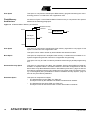
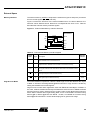
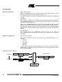
the CPU to address 0000h. RST input has a pull-down resistor allowing power-on reset
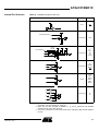
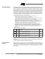
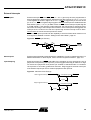
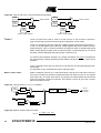
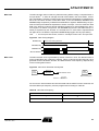
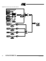
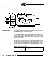
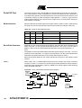
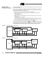
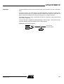
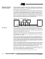
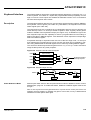
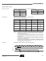
by simply connecting an external capacitor to VDD as shown in Figure 24. A warm reset
can be applied either directly on the RST pin or indirectly by an internal reset source
such as the watchdog timer. Resistor value and input characteristics are discussed in
the Section “DC Characteristics” of the AT8xC51SND1C datasheet. The status of the
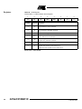
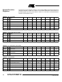
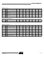
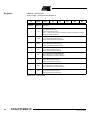
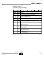
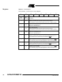
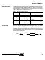
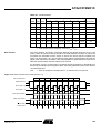
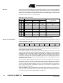
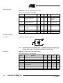
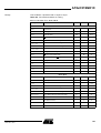
Port pins during reset is detailed in Table 57.
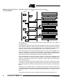
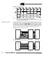
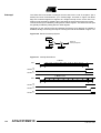
Figure 24. Reset Circuitry and Power-On Reset
From Internal
Reset Source
VDD
P
VDD
To CPU Core
and Peripherals
+
RRST
RST
RST
VSS
RST input circuitry
Power-on Reset
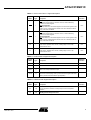
Table 57. Pin Conditions in Special Operating Modes
Mode
Port 0
Port 1
Port 2
Port 3
Port 4
Port 5
MMC
Audio
Floating
High
High
High
High
High
Floating
1
Idle
Data
Data
Data
Data
Data
Data
Data
Data
Power-down
Data
Data
Data
Data
Data
Data
Data
Data
Reset
Note:
Cold Reset
1. Refer to section “Audio Output Interface”, page 73.
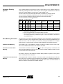
2 conditions are required before enabling a CPU start-up:
•
VDD must reach the specified VDD range
•
The level on X1 input pin must be outside the specification (VIH, VIL)
If one of these 2 conditions are not met, the microcontroller does not start correctly and
can execute an instruction fetch from anywhere in the program space. An active level
applied on the RST pin must be maintained till both of the above conditions are met. A
reset is active when the level V IH1 is reached and when the pulse width covers the
period of time where VDD and the oscillator are not stabilized. 2 parameters have to be
taken into account to determine the reset pulse width:
•
VDD rise time,
•
Oscillator startup time.
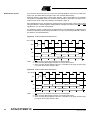
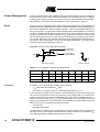
To determine the capacitor value to implement, the highest value of these 2 parameters
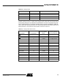
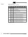
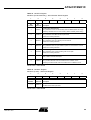
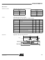
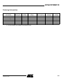
has to be chosen. Table 58 gives some capacitor values examples for a minimum RRST
of 50 KΩ and different oscillator startup and VDD rise times.
46
AT8xC51SND1C
4109E–8051–06/03