1
11.7 EZ-USB FX2 Register Interface
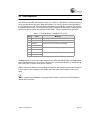
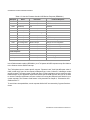
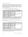
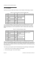
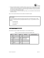
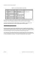
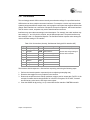
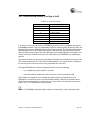
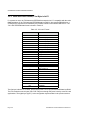
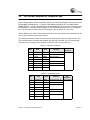
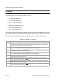
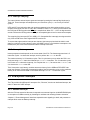
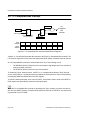
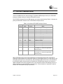
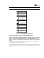
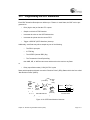
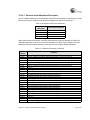
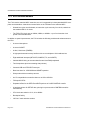
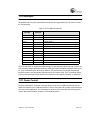
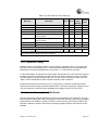
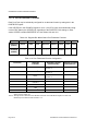
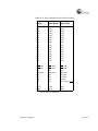
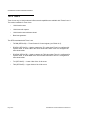
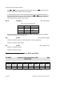
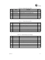
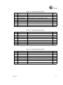
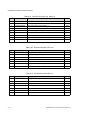
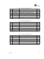
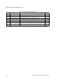
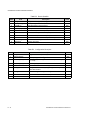
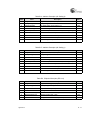
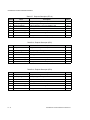
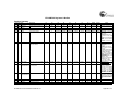
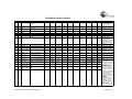
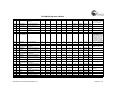
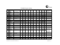
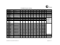
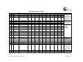
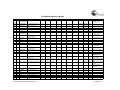
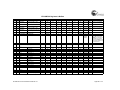
The FX2 peripheral logic (USB, GPIF, FIFOs, etc.) is controlled via a set of memory mapped registers and buffers at addresses 0xE400 through 0xFFFF. These registers and buffers are grouped as
follows:
•
GPIF Waveform Descriptor Tables
•
General configuration
•
Endpoint configuration
•
Interrupts
•
Input/Output
•
USB Control
•
Endpoint operation
•
GPIF/FIFOs
•
Endpoint buffers
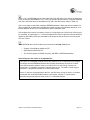
These registers and their functions are described throughout this manual. A full description of
every FX2 register appears in Chapter 15, "Registers"
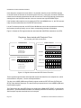
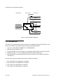
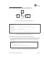
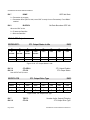
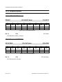
11.8 EZ-USB FX2 Internal RAM
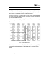
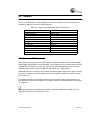
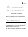
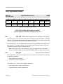
0xFF
Upper 128
SFR Space
0x80
0x7F
Indirect Addr
Direct Addr
0x00
Direct Addr
Lower 128
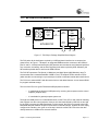
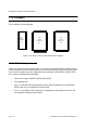
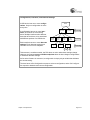
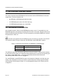
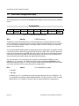
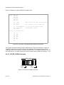
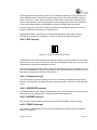
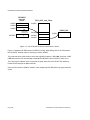
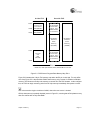
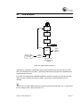
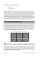
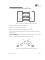
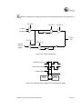
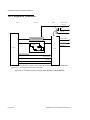
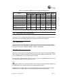
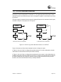
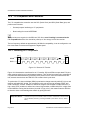
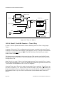
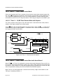
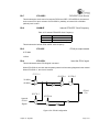
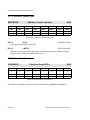
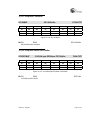
Figure 11-1. FX2 Internal Data RAM
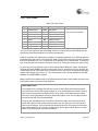
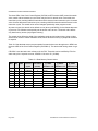
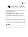
Like the standard 8051, the FX2 contains 128 bytes of Internal Data RAM at addresses 0x00-0x7F
and a partially populated SFR space at addresses 0x80-0xFF. An additional 128 indirectlyaddressed bytes of Internal Data RAM (sometimes called “IDATA”) are also available at addresses
0x80-0xFF.
Chapter 11. CPU Introduction
Page 11-7