1
P UBLIC D OCUMENT
VS1005 A PP N OTE : D EV B OARD P ERFORMANCE
VS1005
All information in this document is provided as-is without warranty. Features are
subject to change without notice.
Revision History
Rev.
1.20
1.12
1.11
1.10
1.02
1.01
1.00
Rev. 1.20
Date
2014-02-24
2013-07-19
2013-02-21
2013-02-19
2013-02-15
2013-02-13
2013-02-12
Author
HH
HH
HH
HH
HH
HH
HH
Description
Added VSOS3 / 0.306 binary.
Modified for better rendering under VSOS 0.24.
Analyzer now includes optional A-weighting filter.
Frequency response measurements redone.
Further minor typo corrections.
Terminology and typo corrections.
Initial version.
2014-02-24
Page 1(32)
VS1005 A PP N OTE : D EV B OARD P ERFORMANCE
HH
Contents
VS1005 AppNote: DevBoard Performance Front Page
1
Table of Contents
2
1 Introduction
5
2 Definitions
5
3 Prerequirements
3.1 Hardware . . . . . . . . . . . . . . . .
3.2 Software . . . . . . . . . . . . . . . . .
3.3 Low-Noise Power Source . . . . . . .
3.4 Audio Signal Generator and Analyzer
.
.
.
.
.
.
.
.
.
.
.
.
.
.
.
.
.
.
.
.
.
.
.
.
.
.
.
.
4 Loopback Test Program
4.1 Test Program Signal Paths . . . . . . . . . . . . .
4.2 Analog Gain Control . . . . . . . . . . . . . . . . .
4.3 Master Volume Control . . . . . . . . . . . . . . . .
4.4 Operation Mode Controls . . . . . . . . . . . . . .
4.4.1 Loopback Mode . . . . . . . . . . . . . . .
4.4.2 Show Unweighted Input Level Mode . . . .
4.4.3 Show A-weighted Input Level Mode . . . .
4.4.4 1000.139 Hz Sine Generator @ 0 dB Mode
4.4.5 1 kHz Sine Generator @ 0 dB Mode . . . .
4.4.6 Sweep Generator @ -1 dB Mode . . . . . .
4.5 Left/Right Out Controls . . . . . . . . . . . . . . . .
Rev. 1.20
.
.
.
.
.
.
.
.
.
.
.
.
.
.
.
.
.
.
.
.
.
.
.
.
.
.
.
.
.
.
.
.
.
.
.
.
.
.
.
.
.
.
.
.
.
.
.
.
.
.
.
.
6
6
6
7
8
.
.
.
.
.
.
.
.
.
.
.
.
.
.
.
.
.
.
.
.
.
.
.
.
.
.
.
.
.
.
.
.
.
.
.
.
.
.
.
.
.
.
.
.
9
10
12
12
13
13
13
14
14
15
15
16
5 Measuring DevBoard Performance
5.1 Measuring Analog Output . . . . . . . . . . . . . . . . . . . . . . . .
5.1.1 Baseline Line Output Measurements . . . . . . . . . . . . . .
5.1.2 Measuring Line Output Dynamic Range . . . . . . . . . . . .
5.1.3 Measuring Line Output Channel Gain Mismatch . . . . . . .
5.1.4 Measuring Line Output Analog Gain Accuracy . . . . . . . .
5.1.5 Measuring Line Output Channel Separation . . . . . . . . . .
5.1.6 Measuring Line Output Signal to Noise and THD+N Ratios .
5.1.7 Measuring Output Frequency Response . . . . . . . . . . . .
5.2 Measuring Analog Input . . . . . . . . . . . . . . . . . . . . . . . . .
5.2.1 Measuring Line Input Background Noise and Dynamic Range
5.2.2 Measuring Maximum Line Input Level . . . . . . . . . . . . .
5.2.3 Measuring Line Input Channel Gain Mismatch . . . . . . . .
5.2.4 Measuring Line Input Channel Separation . . . . . . . . . . .
5.2.5 Measuring Line Input Signal to Noise and THD+N Ratios . .
5.2.6 Measuring Line Input Frequency Response . . . . . . . . . .
.
.
.
.
.
.
.
.
.
.
.
.
.
.
.
.
.
.
.
.
.
.
.
.
.
.
.
.
.
.
.
.
.
.
.
.
.
.
.
.
.
.
.
.
.
17
17
17
18
18
19
19
20
23
25
25
25
26
26
26
27
.
.
.
.
.
.
.
.
.
.
.
.
.
.
.
.
.
.
.
.
.
.
.
.
.
.
.
.
.
.
.
.
.
.
.
.
.
.
.
.
.
.
.
.
.
.
.
.
.
.
.
.
.
.
.
.
.
.
.
.
.
.
.
.
.
.
.
.
.
.
.
.
.
.
.
.
.
.
.
.
.
.
.
.
.
.
.
.
.
.
.
.
.
.
.
.
.
.
.
6 VS1005 Developer Board Performance Summary
29
7 Latest Version Changes
30
2014-02-24
Page 2(32)
VS1005 A PP N OTE : D EV B OARD P ERFORMANCE
HH
8 Contact Information
Rev. 1.20
32
2014-02-24
Page 3(32)
VS1005 A PP N OTE : D EV B OARD P ERFORMANCE
HH
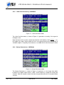
List of Figures
1
2
3
4
5
6
7
8
9
10
11
12
13
14
15
16
17
Rev. 1.20
VS1005 Developer Board. . . . . . . . . . . . . . . . . . . . . . . . . . . .
VS1005 Developer Board with lab power. . . . . . . . . . . . . . . . . . .
VS1005 Developer Board with Li-Ion or LiPo battery. . . . . . . . . . . . .
For proper measurement results, do not power the VS1005 Developer
Board from a PC computer port. Use a stabilized laboratory power or a
battery as shown in Figures 2 and 3. . . . . . . . . . . . . . . . . . . . . .
Loopback mode. . . . . . . . . . . . . . . . . . . . . . . . . . . . . . . . .
Loopback Program 24-bit signal paths. . . . . . . . . . . . . . . . . . . . .
Loopback Test Program A-weighting filter frequency response. . . . . . .
Show Unweighted Input Level mode. . . . . . . . . . . . . . . . . . . . . .
Show Unweighted Input Level mode. . . . . . . . . . . . . . . . . . . . . .
1000.139 Hz Generator mode. . . . . . . . . . . . . . . . . . . . . . . . .
1 kHz Generator mode. . . . . . . . . . . . . . . . . . . . . . . . . . . . .
Sweep Generator mode. . . . . . . . . . . . . . . . . . . . . . . . . . . . .
VS1005 DevBoard output signal to noise and THD+N ratios at different
Analog Gain and Master Volume settings. . . . . . . . . . . . . . . . . . .
VS1005 DevBoard output signal to noise and THD+N ratios at different
output signal levels. . . . . . . . . . . . . . . . . . . . . . . . . . . . . . .
VS1005 DevBoard output frequency response, 20 to 20000 Hz, Line Out.
VS1005 DevBoard output frequency response, 20 to 20000 Hz, Earphone.
DevBoard Input Frequency Response, 20 to 20000 Hz. . . . . . . . . . . .
2014-02-24
6
7
7
8
9
10
11
13
14
14
15
15
21
22
23
24
28
Page 4(32)
VS1005 A PP N OTE : D EV B OARD P ERFORMANCE
HH
1
Introduction
VS1005 is a system DSP processor with integrated high-quality 24-bit audio Analog-toDigital Converters (ADCs) and Digital-to-Analog Converters (DACs).
This document presents the VS1005 Loopback Test Program, and tells how to use it to
measure the performance of the VS1005 Developer Board, or a compatible board. It
also presents example reference values from a randomly selected VS1005 Developer
Board.
2
Definitions
ADC Analog to digital converter.
DAC Digital to analog converter.
dB Decibel, a logarithmic unit that indicates the ratio of two powers. 1 bel, which equals
10 decibels, is a power ratio of 10. With additional qualifiers (like dBfs, or dbV), it
can also be used to quantify absolute signal levels.
dB(A) Decibel, but with the signals run through A Weighting curve before calculation.
A Weighting usually gives results more relevant to how humans hear differences
than measurements done without a weighting curve.
dBfs Decibel full scale. Decibel scale where zero point is bound to a digital full scale
sine wave.
dBV Decibel volt. Decibel scale where zero point is bound to 0 dBV = 1 Vrms.
% Per cent. Sometimes used to present THD instead of the dB scale. To convert from
dB scale to per cent scale, use the following formula: pc = 100 × 10−T HD/20 .
THD Total Harmonic Distortion.
THD+N Total Harmonic Distortion plus Noise.
Vpp Volts, peak-to-peak. A sine signal of 1 Vpp =
1√
2× 2
Vrms.
Vrms Volts, root mean square. A sine
√ signal of 1 Vrms has an amplitude of
its peak-to-peak voltage is 2 × 2 Vpp.
Rev. 1.20
2014-02-24
√
2 V, and
Page 5(32)
VS1005 A PP N OTE : D EV B OARD P ERFORMANCE
HH
3
Prerequirements
The following prerequirements need to be met so as to be able to get relieable results.
USB−A
Line In
BT
Line Out
−
+
Headphones
Hardware
USB−AB
3.1
JP5
JP6
GND
TX
RX
3V3
5V
CN9
Figure 1: VS1005 Developer Board.
The VS1005 Developer Board v1.4 or newer, as shown in Figure 1, or a compatible
board, is required.
Set the Line In jumper JP5 as shown in the figure.
3.2
Software
The Loopback Test Program can be downloaded from
http://www.vlsi.fi/en/support/software/vs1005applications.html .
Unzip the package.
If using VSOS3 series 0.306 or newer, copy AudioLoopback.ap3 to the SD card main
folder. To work, the program requires that the 2-way audio driver AUDIO.DL3 (available
as a template in VSIDE) has been installed to the SYS/ folder.
If using VSOS 2 series 0.23 or newer, copy AudioLoopback.app to the SD card main
folder.
Boot VSOS and start the program.
Rev. 1.20
2014-02-24
Page 6(32)
VS1005 A PP N OTE : D EV B OARD P ERFORMANCE
HH
3.3
Low-Noise Power Source
Line In
USB−A
Line Out
Lab power
5V
Headphones
−
+
BT
USB−AB
For best results, a good quality power source with low noise on the audio band is required.
JP5
JP6
GND
TX
RX
3V3
5V
CN9
Figure 2: VS1005 Developer Board with lab power.
Li−Ion
or
LiPo
3.7 V
Line In
Line Out
USB−A
Headphones
−
+
BT
USB−AB
Recommended power sources are either a 5 V lab power, connected to CN9 pins GND
and 5 V, as shown in Figure 2. The lab power may also be connected to the 5 V pin of
either the USB-AB or USB-A connector on the VS1005 Developer Board.
JP5
JP6
GND
TX
RX
3V3
5V
CN9
Figure 3: VS1005 Developer Board with Li-Ion or LiPo battery.
Another recommended way of powering the VS1005 Developer Board is to connect a
3.7 V Li-Ion or LiPo battery to the BT connector, as shown in Figure 3.
Note that the VS1005 Developer Board is equipped with charging logic for the battery.
So when you connect the battary and any 5 V power source to the developer board, the
battery will automatically charge. As long as the batter is charging, a CHARGE LED
close to the BT connector will be lit.
Rev. 1.20
2014-02-24
Page 7(32)
VS1005 A PP N OTE : D EV B OARD P ERFORMANCE
Line In
Line Out
USB−A
Headphones
−
+
BT
USB−AB
HH
JP5
JP6
GND
TX
RX
3V3
5V
CN9
Line In
Line Out
USB−A
Headphones
−
+
BT
USB−AB
USB
JP5
JP6
GND
TX
RX
3V3
5V
CN9
Line In
Line Out
USB−A
Headphones
−
+
BT
USB−AB
USB
JP5
JP6
GND
TX
RX
3V3
5V
CN9
USB
Figure 4: For proper measurement results, do not power the VS1005 Developer Board
from a PC computer port. Use a stabilized laboratory power or a battery as shown in
Figures 2 and 3.
As shown in Figure 4, do not power the VS1005 Developer Board directly from computer
USB using the USB-AB or USB-A connectors, or with a USB-to-RS232 cable using the
RS232 connector. PC powers are notoriously noisy and will cause unnecessary noise
in both the inputs and outputs. For the same reason, do not use cheap AC-to-USB
adapters.
Note also that even if you power the VS1005 Developer Board from a good power
source, an electrical connection to a PC can still degrade performance. So, before
doing any measurement, disconnect any cables between the DevBoard and the PC that
you don’t need for the specific measurement, particularly the RS232 cable.
3.4
Audio Signal Generator and Analyzer
A high-quality audio signal generator and analyzer, like the Rohde & Schwarz UPV
Audio Analyzer / Signal Generator, is required. PC sound cards are in general not
nearly of sufficient quality to be able to show the dynamic range potential of the VS1005
Developer Board.
Note: A volt meter in AC mode is not sufficient to measure the power of output signals.
Because of the sigma-delta digital-to-analog converters of the VS1005, the outputs contain out-of-hearing-band white noise that cannot be heard, but which a volt meter will
see.
Rev. 1.20
2014-02-24
Page 8(32)
VS1005 A PP N OTE : D EV B OARD P ERFORMANCE
HH
4
Loopback Test Program
Figure 5: Loopback mode.
The Loopback Test Program looks as shown in Figure 5.
The top of the display shows the result of the RMS & Peak analyzer if Show Unweighted
Input Level mode (Chapter 4.4.2) or Show A-weighted Input Level mode (Chapter 4.4.3)
is selected. Otherwise they will show zeros.
Next is the Analog Gain control (Chapter 4.2).
Followed by that is the Master Volume adjustment control (Chapter 4.3).
Finally are the Operation Mode controls (Chapter 4.4) and Left/Right Output selection
controls (Chapter 4.5).
Rev. 1.20
2014-02-24
Page 9(32)
VS1005 A PP N OTE : D EV B OARD P ERFORMANCE
HH
4.1
Test Program Signal Paths
VS1005
Loopback program
Analog Output Gain
Master Volume
Left Out
Right Out
Signal
Generator
LEFT IN
RIGHT IN
ADC
DAC
Ring
buffer
ADC
DAC
LEFT OUIT
RIGHT OUT
A
RMS & Peak
Analyzer
A
Figure 6: Loopback Program 24-bit signal paths.
The Test Program signal paths are shown in Figure 6.
Data is read at 48 kHz from the left and right ADCs that are connected to analog line
inputs Left In and Right In. This signal is divided into two paths: it is forwarded to the
RMS and Peak Analyzer either directly or through an A-weighting filter. The signal is
also forwarded without filtering to the ring buffer input selection multiplexer.
Figure 7 shows the frequency response of the A-weighting filter.
The ring buffer input selection multiplexer selects between the Left and Right inputs and
the Signal Generator, and writes the resulting data to the Ring Buffer.
The Ring Buffer delay is approximately 0.17 ms. (Note: the hardware in the ADC and
DAC cause their own delays which are significantly larger.)
The left and right outputs of the Ring Buffer is, depending on Left Out and Right Out
controls, multiplied by either 0 or 1, and sent at 48 kHz through the VS1005 hardware
volume control, DAC, and Analog Output Gain, to the analog outputs Left Out and Right
Out.
Rev. 1.20
2014-02-24
Page 10(32)
VS1005 A PP N OTE : D EV B OARD P ERFORMANCE
HH
A−weighting curve, 20−20000 Hz
0
amp/dB
−10
−20
−30
−40
−50
10^{2}
10^{3}
f/Hz
10^{4}
Figure 7: Loopback Test Program A-weighting filter frequency response.
Rev. 1.20
2014-02-24
Page 11(32)
VS1005 A PP N OTE : D EV B OARD P ERFORMANCE
HH
4.2
Analog Gain Control
Analog Gain control lets the user to set one of VS1005’s analog gain controls: -12 dB,
-6 dB, or 0 dB. At lower settings background white noise is significantly lower, but harmonic distortion may be slightly higher with full-scale signals, and if Master Volume
(Chapter 4.3) is set close to maximum.
Generally speaking best audio can be obtained when Analog Gain is at its lowest setting
that offers enough sound pressure.
Note: Analog Gain controls are not exact. They are measured in Chapter 5.1.4.
4.3
Master Volume Control
The digital Master Volume control lets the user set a digital volume control. This digital
volume control operates in the 24-bit digital domain, which makes its quality very high.
The user can adjust master volume in 1 dB and 6 dB steps.
Rev. 1.20
2014-02-24
Page 12(32)
VS1005 A PP N OTE : D EV B OARD P ERFORMANCE
HH
4.4
4.4.1
Operation Mode Controls
Loopback Mode
The basic mode in the Loopback test program is the Loopback mode, shown in Figure 5
on Page 9. This mode is intended for measuring the performance of the board using an
audio analyzer.
In this mode, the analog inputs are read and copied through the ring buffer directly the
the analog output. Otherwise the program does as little as possible as as not to cause
any extra EMC emissions that would interfere with best performance.
4.4.2
Show Unweighted Input Level Mode
Figure 8: Show Unweighted Input Level mode.
The Show Unweighted Input Level mode, as shown in Figure 8, shows the current left
and right line input peak and RMS levels on the LCD screen.
The peak level is a 24-bit hexadecimal number with 0x800000 (displayed as 800000) as
the maximum value.
The RMS level is on the decibel scale in relation to a full-scale sine input wave.
In this mode the digital input signal is run through a DC offset removal filter. Otherwise
is not filtered.
This mode is best suited for input frequency response measurements.
Rev. 1.20
2014-02-24
Page 13(32)
VS1005 A PP N OTE : D EV B OARD P ERFORMANCE
HH
4.4.3
Show A-weighted Input Level Mode
Figure 9: Show Unweighted Input Level mode.
The Show A-weighted Input Level mode, as shown in Figure 9, works just like Show
Unweighted Input Level mode as shown in Chapter 4.4.2, except that the input signal is
run through an A-weighting filter before analysis.
The frequency response of the A-weighting filter is prestented in Figure 7 on Page 11.
This mode is best suited for e.g. dynamic range and channel separation measurements.
4.4.4
1000.139 Hz Sine Generator @ 0 dB Mode
Figure 10: 1000.139 Hz Generator mode.
The 1000.139 Hz Sine Generator, as shown in Figure 10, offers a high-quality sine signal
output at full digital range. It is recommended for audio quality measurements.
Rev. 1.20
2014-02-24
Page 14(32)
VS1005 A PP N OTE : D EV B OARD P ERFORMANCE
HH
4.4.5
1 kHz Sine Generator @ 0 dB Mode
Figure 11: 1 kHz Generator mode.
The 1 kHz Sine Generator, as shown in Figure 11, generates an exactly 1 kHz signal at
full digital scale.
Note that because the system sample rate of 48 kHz is divisable by 1 kHz ( 48000Hz
1000Hz = 48),
this mode may show a signal spectrum that is not representative of the true quality of
VS1005’s outputs. For quality measurements, use 1000.139 Hz Sine Generator instead.
4.4.6
Sweep Generator @ -1 dB Mode
Figure 12: Sweep Generator mode.
The Sweep Generator, as shown in Figure 12, generates a sine sweep from 20 Hz
to 20 kHz at a digital signal level of -1 dBfs. Each frequency is output for exactly two
seconds. After the sweep has been finished, the generator waits for 10 seconds before
a restart.
Rev. 1.20
2014-02-24
Page 15(32)
VS1005 A PP N OTE : D EV B OARD P ERFORMANCE
HH
4.5
Left/Right Out Controls
The Left Out and Right Out controls can be used to individually turn the left and right
outputs on and off.
Rev. 1.20
2014-02-24
Page 16(32)
VS1005 A PP N OTE : D EV B OARD P ERFORMANCE
HH
5
Measuring DevBoard Performance
This Chapter will show how to measure the VS1005 Developer Board performance, and
gives examples of a randomly chosed DevBoard for each case.
5.1
Measuring Analog Output
Set up your audio analyzer so that it analyses only the audio range 20 Hz to 20 kHz, and
that it used A-weighting.
5.1.1
Baseline Line Output Measurements
Start by measuring the following values which will be needed later. Set the measuring
program as follows:
1. Analog Gain as stated in the table below, Master Volume 0 dB, 1000.139 Hz Generator, Left Out On except where noted, Right Out On except where noted, analyzer
input impedance high.
Boxes that are marked N/A are not needed. The data for the example card is presented
below.
Output levels at different Analog Gain Settings, Volume 0 dB
Symbol
Analog
Output level
Gain/
Left/
Right/
Mean/
dB mVrms mVrms mVrms
Full swing output OUT0_L/R/M
0
931
939
935
Output at -6 dB
OUT6_L/R/M
-6
476
479
478
Output at -12 dB OUT12_L/R/M
-12
242
243
243
Left muted
OUT0MUTEL_L
0
0.032
N/A
N/A
Right muted
OUT0MUTER_R
0
N/A
0.042
N/A
Muted at 0 dB
OUT0MUTE_L/R/M
0 0.0128 0.0118 0.0123
Muted at -6 dB
OUT6MUTE_L/R/M
-6 0.0078 0.0072 0.0075
Muted at -12 dB
OUT12MUTE_L/R/M
-12 0.0055 0.0055 0.0055
Name
Results for the left and right channel should always be similar and symmetrical. If they
are far from each other, there is a problem with the measurement setup, cables, PCB,
or IC.
Rev. 1.20
2014-02-24
Page 17(32)
VS1005 A PP N OTE : D EV B OARD P ERFORMANCE
HH
5.1.2
Measuring Line Output Dynamic Range
Dynamic range is the ratio of the energy of the strongest signal that can be output to the
background noise on an empty channel.
To calculate the dynamic range over the full analog gain range, and using the values
from the baseline measurements as explained in Chapter 5.1.1, the dynamic range is
calculated as follows:
T 0_ M
log OU TOU
12M U T E _M
dr = 20 ×
dB(A).
log 10
Example:
dr = 20 ×
935
log 0.0055
log 10
= 104.6 dB(A).
Switching Analog Gain causes a slight glitch in sound. So in an application where the
user doesn’t change the volume level, it should be used with caution. For an application
that uses Analog Gain, we can calculate the dynamic range as follows:
drg0 = 20 ×
log
_
OU T 0 M
OU T 0M U T E M
_
log 10
dB(A).
Example:
drg0 = 20 ×
5.1.3
935
log 0.0123
log 10
= 97.6 dB(A).
Measuring Line Output Channel Gain Mismatch
Left/Right channel mismatch tells the mismatch between the left and right analog outputs. This mismatch depends on the setting of the Analog Gain, but not the digital
Master Volume. So it needs to be calculated for different Analog Gain settings.
Using the values from the baseline measurements as explained in Chapter 5.1.1, the
line output L-R channel gain mismatches are calculated as follows:
_
_ dB.
log 10
OU T 6_L
log OU
T 6_ R
ec−6 = 20 ×
dB.
log 10
OU T 12_L
log OU T 12_R
ec−12 = 20 ×
dB.
log 10
ec0 = 20 ×
log
OU T 0 L
OU T 0 R
Example:
931
log 937
log 10 = −0.07 dB.
log 476
-6 dB channel mismatch is ec−6 = 20 × log479
10 = −0.05 dB.
log 242
-12 dB channel mismatch is ec−12 = 20 × log243
10 = −0.04 dB.
0 dB channel mismatch is ec0 = 20 ×
Rev. 1.20
2014-02-24
Page 18(32)
VS1005 A PP N OTE : D EV B OARD P ERFORMANCE
HH
5.1.4
Measuring Line Output Analog Gain Accuracy
Using the values from the baseline measurements as explained in Chapter 5.1.1, the
analog gain is calculated as follows:
egx = 20 ×
log
_
_
OU T x M
OU T 0 M
log 10
dB.
Example:
Actual analog gain for the -6 dB setting is eg−6 = 20 ×
Actual analog gain for the -12 dB setting is eg−12 = 20
5.1.5
478
log 935
log 10 = −5.83 dB.
log 243
× log935
10 = −11.70 dB.
Measuring Line Output Channel Separation
Output channel separation tells how much the left audio channel bleeds to the right, and
vice versa.
Using the values from the baseline measurements as explained in Chapter 5.1.1, the
left/right channel separation is calculated as follows:
sl = 20 ×
log
_
OU T 0 R
OU T 0M U T EL
log 10
_L dB(A).
T 0_L
log OU TOU
0M U T EL_R
sr = 20 ×
dB(A).
log 10
Choose the lower value as your channel separation.
Example:
939
log 0.032
log 10
log 931
× log0.042
10
sl = 20 ×
= 89.4 dB(A).
sr = 20
s = 86.9 dB(A)
= 86.9 dB(A).
If you want to test the earphone output under maximum load, you may connect both the
left and right earphone channel to CBUF with two 30 Ω resistors, then measure again.
Note that output channel separation is always a combination of the performance of the
PCB and the IC. If there are vias on the PCB with even a 0.1 Ω resistance, it will severely
affect output channel separation if a low-impedance load is connected to the device.
Rev. 1.20
2014-02-24
Page 19(32)
VS1005 A PP N OTE : D EV B OARD P ERFORMANCE
HH
5.1.6
Measuring Line Output Signal to Noise and THD+N Ratios
Measure the A-weighted noise and THD+N voltages for each channel with these parameters:
1. Analog Gain as needed, Master Volume as needed, 1000.139 Hz Generator, Left
Out On, Right Out On, analyzer input impedance high.
Depending on your requirements, repeat with different Master Volume, Gain Settings,
and analyzer impedance settings. Plot as needed.
Example for left channel on DevBoard:
Output noise and THD+N ratios
Analog Gain 0 dB Analog Gain -6 dB Analog Gain -12 dB
Volume
S/N
THD+N
S/N
THD+N
S/N
THD+N
/dB / dB(A)
/ dB(A) / dB(A)
/ dB(A) / dB(A)
/ dB(A)
0
92.5
65.8
92.3
69.9
90.8
74.6
-1
92.7
67.1
92.0
71.1
90.7
76.0
-2
92.5
69.0
91.6
72.1
90.1
77.1
-3
92.0
70.4
91.3
73.2
89.4
78.1
-4
91.5
71.3
90.8
74.2
88.7
79.1
-5
91.3
71.2
90.1
75.2
88.0
79.9
-6
90.6
72.2
89.5
76.1
87.0
80.6
-9
88.4
75.6
87.1
78.9
84.4
81.8
-12
85.9
77.5
84.6
80.6
81.6
80.8
-18
80.2
79.0
78.7
78.2
75.7
75.5
-24
73.5
73.5
72.2
72.0
69.5
69.4
-36
61.5
61.5
60.2
60.1
57.5
57.4
-48
49.1
49.1
47.9
47.6
45.2
45.3
-60
37.1
38.0
35.8
36.8
33.1
33.0
-72
25.0
25.0
23.9
23.6
21.2
21.2
-78
19.0
19.0
18.0
17.7
15.4
15.3
-84
13.2
13.4
12.1
11.9
9.61
9.61
-90
7.81
8.01
6.41
6.71
5.11
5.11
1
Rev. 1.20
Numbers below 10 dB(A) are unreliable with the analyzer used for this example.
2014-02-24
Page 20(32)
VS1005 A PP N OTE : D EV B OARD P ERFORMANCE
HH
Signal−to−noise or Signal−to−THD+N ratio / dB(A)
VS1005 DevBoard output Noise and THD+N ratios at different settings
90
80
70
60
50
40
30
20
10
−90
−80
−70
Analog Gain 0 dB, S/N
Analog Gain 0 dB, THD+N
Analog Gain −6 dB, S/N
Analog Gain −6 dB, THD+N
Analog Gain −12 dB, S/N
Analog Gain −12 dB, THD+N
−60
−50
−40
−30
−20
−10
Master Volume / dB
0
Figure 13: VS1005 DevBoard output signal to noise and THD+N ratios at different Analog Gain and Master Volume settings.
Figure 13 presents graphically the DevBoard noise and THD+N ratios for different volume settings at different analog gain settings.
Rev. 1.20
2014-02-24
Page 21(32)
VS1005 A PP N OTE : D EV B OARD P ERFORMANCE
HH
Signal−to−noise or Signal−to−THD+N ratio / dB(A)
VS1005 DevBoard output Noise and THD+N ratios at different settings
90
80
70
60
50
40
30
20
10
10^{−2}
10^{−1}
Analog Gain 0 dB, S/N
Analog Gain 0 dB, THD+N
Analog Gain −6 dB, S/N
Analog Gain −6 dB, THD+N
Analog Gain −12 dB, S/N
Analog Gain −12 dB, THD+N
10^{0}
10^{1}
10^{2}
Output signal level / mVrms
10^{3}
Figure 14: VS1005 DevBoard output signal to noise and THD+N ratios at different output
signal levels.
Figure 14 presents graphically the DevBoard noise and THD+N ratios in relation to the
output signal level.
The maximum signal level for Master Volume = 0 dB is 935 Vrms, 478 Vrms, and 243 mVrms
for Analog Gains -0 dB, -6 dB, and -12 dB, respectively, as calculated in Chapter 5.1.1.
As can be seen from the Figure, in general the best performance at a given output level
can be obtained by using the lowest possible Analog Gain.
Example: For an output of 10 mVrms, Analog Gain -12 dB gives a THD+N ratio of approximately 66 dB(A), while Analog Gain -6 dB and 0 dB give THD+N ratios of 62 dB(A)
and 58 dB(A), respectively.
Rev. 1.20
2014-02-24
Page 22(32)
VS1005 A PP N OTE : D EV B OARD P ERFORMANCE
HH
5.1.7
Measuring Output Frequency Response
Set your signal analyzer to sine sweep analyzer mode. Set the DevBoard as follows:
1. Analog Gain 0 dB, Master Volume 0 dB, Sweep Generator, Left Out On, Right Out
On, analyzer input impedance high.
The two outputs, Line Out and Earphone, are connected differently on the DevBoard:
the Line Out has an analog low-pass filter. Because of this, the frequency responses
are slightly different.
Figure 15: VS1005 DevBoard output frequency response, 20 to 20000 Hz, Line Out.
Example DevBoard Line Out frequency response is shown in Figure 15. The frequency
response is ±0.15 dB between 20 and 20000 Hz.
Rev. 1.20
2014-02-24
Page 23(32)
VS1005 A PP N OTE : D EV B OARD P ERFORMANCE
HH
Figure 16: VS1005 DevBoard output frequency response, 20 to 20000 Hz, Earphone.
Example DevBoard Earphone frequency response is shown in Figure 16. The frequency
response is ±0.03 dB between 20 and 20000 Hz.
Rev. 1.20
2014-02-24
Page 24(32)
VS1005 A PP N OTE : D EV B OARD P ERFORMANCE
HH
5.2
Measuring Analog Input
To measure the analog input, you need a high-quality audio signal generator. Connect
the generator to the left and right line input of the DevBoard.
5.2.1
Measuring Line Input Background Noise and Dynamic Range
First measure the input background noise without any other connectors to the board
than the power connector from either the external high-quality lab power or the Li-Ion /
LiPo battery. Then set the following parameters:
1. Analog Gain -12 dB, Master Volume 0 dB, Show A-Weighted Input Level, Left Out
On, Right Out On.
You should now see a very low RMS number on the display. It should be -95 dB(A) or
better. An example if this display is shown in Figure 9 on Page 14. This background
noise level is also the dynamic range of the system.
Example: The example DevBoard’s background noise level is -99 dB(A) for the left channel and -98 dB(A) for the right channel. The dynamic range is thus 98 dB(A).
Note that there is some board-to-board variation, so even if the numbers are in the
95 dB(A) range, it doesn’t necessarily mean that there are any specific problems with
the board.
Now connect the line input to the signal generator. If there is a change in the RMS value
then either your cable or your signal generator is not of sufficient quality to measure the
DevBoard, or there is a ground loop that is affecting your measurements.
5.2.2
Measuring Maximum Line Input Level
Set you signal generator to generate a low voltage, e.g. 100 mVrms, sine signal. Then
set the DevBoard to:
1. Analog Gain -12 dB, Master Volume 0 dB, Show Unweighted Input Level, Left Out
On, Right Out On.
You should now see RMS values of approximately -21.3 dB, like on the Example DevBoard.
Slowly increase the voltage until the Peak detectors just cannot reach their maximum
value 0x800000. This should happen at approximately 1.16 Vrms, like on the Example
DevBoard.
Rev. 1.20
2014-02-24
Page 25(32)
VS1005 A PP N OTE : D EV B OARD P ERFORMANCE
HH
5.2.3
Measuring Line Input Channel Gain Mismatch
Set you signal generator to generate a low voltage, e.g. 100 mVrms, sine signal. Then
set the DevBoard to:
1. Analog Gain -12 dB, Master Volume 0 dB, Show Unweighted Input Level, Left Out
On, Right Out On.
The difference between the left and right channel level is the input channel gain mismatch.
Example: Devboard shows left RMS at -21.55 dB and right RMS at -21.53 dB, so the
mismatch is −21.55 − −21.53 = −0.02 dB.
5.2.4
Measuring Line Input Channel Separation
Set the DevBoard to:
1. Analog Gain -12 dB, Master Volume 0 dB, Show A-weighted Input Level, Left Out
On, Right Out On.
Set your signal generator to generate a 1 V signal to the left channel and no signal to the
right channel. Take the difference between the right and left RMS outputs on the LCD.
Repeat with channels switched. The results should be almost identical. Use the value
that’s worse.
Example: Left channel at -1.50 dB(A) and right channel at -92.01 dB(A), so channel
separation is −1.50 − −92.01 = 90.51 dB(A). When reversed right level is is -93.70 dB(A)
and left is -1.48 dB(A), so separation is −1.48−−93.70 = 92.22 dB(A). The worse number
is 90.5 dB(A), which is the channel separation.
5.2.5
Measuring Line Input Signal to Noise and THD+N Ratios
The VS1005 Developer Board and its current software doesn’t offer any easy way to
determine input Noise and THD+N figures, although in the future an updated version
may be released which outputs the analog input signal digitally.
However, a loopback test gives the lowest possible performance values as follows. Set
DevBoard to:
1. Analog Gain -12 dB, Master Volume 0 dB, Loopback, Left Out On, Right Out On,
analyzer input impedance high.
Generate different amplitude signals, upto 1.1 Vrms, to the DevBoard, and use your
audio analyzer to analyze the results. For signals lower than 100 mVrms, set Analog
Gain to 0 dB.
Rev. 1.20
2014-02-24
Page 26(32)
VS1005 A PP N OTE : D EV B OARD P ERFORMANCE
HH
5.2.6
Measuring Line Input Frequency Response
Set the DevBoard to:
1. Analog Gain -12 dB, Master Volume 0 dB, Show Unweighted Input Level, Left Out
On, Right Out On
Use an e.g. 1 Vrms signal on your signal generator at different frequencies. Record the
RMS value for each frequency.
Then, normalize the result around 0 dB by subtracting the mean passband value from
all the results.
The following table presents the frequency response for the left channel. The right
channel was identical within ±0.02 dB, so it is not presented here.
Freq / Hz
20
30
40
50
100
200
500
1000
2000
5000
10000
12000
14000
16000
17000
18000
18500
19000
19500
20000
1
Input frequency response, left channel
Meas Level / dB Offset1 / dB Corrected / dB
-1.49
1.50
+0.01
-1.46
1.50
+0.04
-1.45
1.50
+0.05
-1.45
1.50
+0.05
-1.44
1.50
+0.06
-1.44
1.50
+0.06
-1.44
1.50
+0.06
-1.45
1.50
+0.05
-1.47
1.50
+0.03
-1.46
1.50
+0.04
-1.49
1.50
+0.01
-1.48
1.50
+0.02
-1.50
1.50
0.00
-1.53
1.50
-0.03
-1.53
1.50
-0.03
-1.52
1.50
-0.02
-1.52
1.50
-0.02
-1.54
1.50
-0.04
-1.55
1.50
-0.06
-1.57
1.50
-0.07
Offset has been selected in such a way that the results are normalized around 0 dB.
The input frequency response as shown in the table above and Figure 17 shows a
frequency response of ±0.07 dB at 20 to 20000 Hz.
Rev. 1.20
2014-02-24
Page 27(32)
VS1005 A PP N OTE : D EV B OARD P ERFORMANCE
HH
VS1005 DevBoard input frequency response
1
level/dB
0.5
0
−0.5
−1
10^{2}
10^{3}
f/Hz
10^{4}
Figure 17: DevBoard Input Frequency Response, 20 to 20000 Hz.
Rev. 1.20
2014-02-24
Page 28(32)
VS1005 A PP N OTE : D EV B OARD P ERFORMANCE
HH
6
VS1005 Developer Board Performance Summary
Below are tables that show a summary of the measurements results to a random VS1005
Development Board. When you design your own board, please verify that the results you
get are consistent with the ones presented here.
VS1005 DevBoard Line/Earphone Output Performance
Parameters
Result Unit
Presented in
Line out maximum signal level
935 mVrms Chapter 5.1.1
Line out dynamic range
104.6 dB(A) Chapter 5.1.2
Line out dynamic range, Analog Gain 0 dB
97.6 dB(A) Chapter 5.1.2
Line out channel gain mismatch, A.Gain 0 dB
-0.07 dB
Chapter 5.1.3
Line out channel gain mismatch, A.Gain -6 dB
-0.05 dB
Chapter 5.1.3
Line out channel gain mismatch, A.Gain -12 dB
-0.04 dB
Chapter 5.1.3
Line out real analog gain, Analog Gain -6 dB
-5.83 dB
Chapter 5.1.4
Line out real analog gain, Analog Gain -12 dB
-11.70 dB
Chapter 5.1.4
Line out channel separation
86.9 dB(A) Chapter 5.1.5
Line out signal to noise, A.Gain 0 dB, Volume 0 dB
92.5 dB(A) Chapter 5.1.6
Line out signal to noise, A.Gain 0 dB, Volume -18 dB
80.2 dB(A) Chapter 5.1.6
Line out THD+N, A.Gain 0 dB, Volume 0 dB
65.8 dB(A) Chapter 5.1.6
Line out THD+N, A.Gain 0 dB, Volume -18 dB
79.0 dB(A) Chapter 5.1.6
Line out frequency response, 20-20000 Hz
±0.15 dB
Chapter 5.1.7
Earphone frequency response, 20-20000 Hz
±0.03 dB
Chapter 5.1.7
VS1005 DevBoard Line Input Performance
Parameters
Result Unit
Line in dynamic range
98
dB(A)
Line in maximum signal level
1.16
Vrms
Line in channel gain mismatch
-0.02 dB
Line in channel separation
90
dB(A)
Line in frequency response, 20-20000 Hz
±0.07 dB
Rev. 1.20
2014-02-24
Presented in
Chapter 5.2.1
Chapter 5.2.2
Chapter 5.2.3
Chapter 5.2.4
Chapter 5.2.6
Page 29(32)
VS1005 A PP N OTE : D EV B OARD P ERFORMANCE
HH
7
Latest Version Changes
Version 1.20, 2014-02-24
Added executable file for VSOS3 / 0.306. See Chapter 3.2, Software, for details.
Functionality is unchanged.
Version 1.12, 2013-07-19
The display has been slightly changed to better render under VSOS 0.24. Figure 5,
Loopback mode, has been replaced with one with the VSOS 0.24 look.
Functionality is unchanged.
Version 1.11, 2013-02-21
For this release the pre-filter was replaced with two alternative signal analyzer paths:
unweighted and A-weighted. As a consequence, the following changes took place:
• Changed Figure 6, Loopback Program 24-bit signal paths.
• Replaced two pre-filter frequency response curves with Figure 7, Loopback Test
Program A-weighting filter frequency response.
• Replaced Chapter Show Input Level Mode with Chapters 4.4.2, Show Unweighted
Input Level Mode, and 4.4.3, Show A-weighted Input Level Mode.
• Rewrote significant portions of Chapter 5.2, Measuring Analog Input, to include
measurements done with the new unweighted and A-weighted filters.
Version 1.10, 2013-02-19
For this release the frequency response measurements were redone. Now they are
done better, and the results are much more representetive of VS1005’s capabilities.
• Added Chapter 2, Definitions.
• Modified Loopback Test Program’s Sweep Generator output. With the new output,
redid the line output frequency response and added earphone frequency response
to Chapter 5.1.7.
• Corrected typos and slightly changed wordings in several Chapters.
• Corrected Prefilter frequency response curves in Figures (removed in v1.11) and
(removed in v1.11). The corrected curves were then applied to the correction table
in Chapter 5.2.6, and also the frequency response curve in Figure 17.
Rev. 1.20
2014-02-24
Page 30(32)
VS1005 A PP N OTE : D EV B OARD P ERFORMANCE
HH
Version 1.02, 2013-02-15
• Further typo corrections.
• Software version number changed to 1.02, no other changes to software.
Version 1.01, 2013-02-13
Terminology and typo corrections, particularly to table in Chapter 6, DevBoard Performance Summary.
Version 1.00, 2013-02-12
Initial version.
Rev. 1.20
2014-02-24
Page 31(32)
VS1005 A PP N OTE : D EV B OARD P ERFORMANCE
HH
8
Contact Information
VLSI Solution Oy
Entrance G, 2nd floor
Hermiankatu 8
FI-33720 Tampere
FINLAND
Fax: +358-3-3140-8288
Phone: +358-3-3140-8200
Commercial e-mail: [email protected]
URL: http://www.vlsi.fi/
For technical support or suggestions regarding this document, please participate at
http://www.vsdsp-forum.com/
For confidential technical discussions, contact
[email protected]
Rev. 1.20
2014-02-24
Page 32(32)