1
E
PENTIUM® PRO PROCESSOR AT 150, 166, 180, and 200 MHz
3.14.
GTL+ Bus Specifications
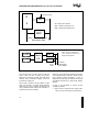
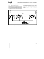
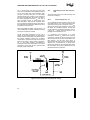
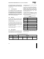
The GTL+ bus must be routed in a daisy-chain
fashion with termination resistors at each end of
every signal trace. These termination resistors are
placed between the ends of the signal trace and the
VTT voltage supply and generally are chosen to
approximate the board impedance. The valid high
and low levels are determined by the input buffers
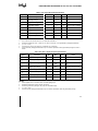
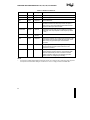
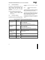
using a reference voltage called VREF. Table 8 lists
the nominal specifications for the GTL+ termination
voltage (VTT) and the GTL+ reference voltage (VREF).
It is important that the printed circuit board
impedance be specified and held to a ±20%
tolerance, and that the intrinsic trace capacitance for
the GTL+ signal group traces is known. For more
details on GTL+, see Section 4.
Table 8. GTL+ Bus Voltage Specifications
Symbol
Parameter
Min
Typical
Max
Units
Notes
VTT
Bus Termination
Voltage
1.35
1.5
1.65
V
±10%
VREF
Input Reference
Voltage
2/3 VTT-2%
2/3 VTT
2/3 VTT +2%
V
±2%, 1
NOTES:
•
VREF should be created from VTT by a voltage divider of 1% resistors.
3.15.
AC Specifications
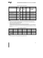
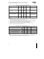
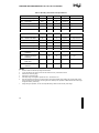
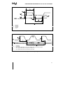
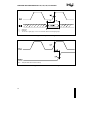
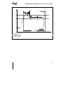
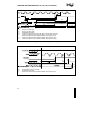
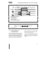
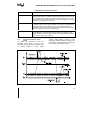
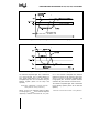
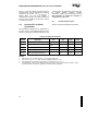
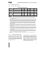
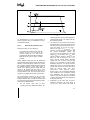
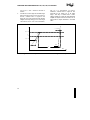
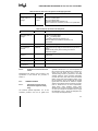
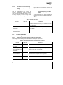
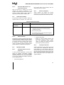
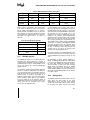
Table 9 through Table 16 list the AC specifications
associated with the Pentium Pro processor. Timing
Diagrams begin with Figure 13. The
AC
specifications are broken into categories. Table 9
contains the clock specifications, Table 11 and
Table 12 contain the GTL+ specifications, Table 13 is
the 3.3 V tolerant Signal group specifications,
Table 14 contains timings for the reset conditions,
24
Table 15 covers APIC bus timing, and Table 16
covers Boundary Scan timing.
All AC specifications for the GTL+ signal group are
relative to the rising edge of the BCLK input. All
GTL+ timings are referenced to VREF for both ‘0’ and
‘1’ logic levels unless otherwise specified.
Care should be taken to read all notes associated
with a particular timing parameter.