1
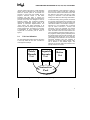
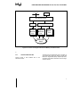
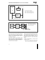
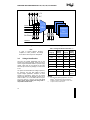
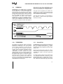
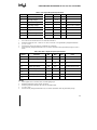
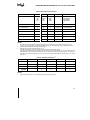
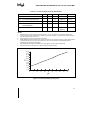
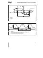
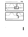
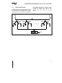
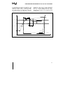
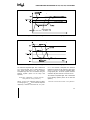
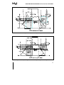
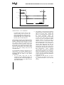
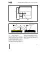
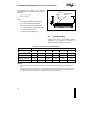
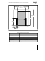
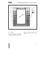
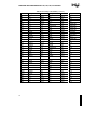
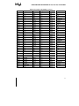
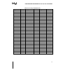
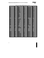
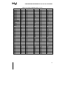
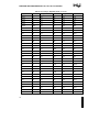
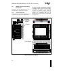
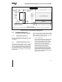
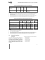
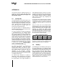
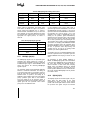
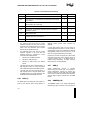
PENTIUM® PRO PROCESSOR AT 150, 166, 180, and 200 MHz
THD’ is the receiver’s hold time plus board clock
driver and clock distribution skew minus the driver’s
on-chip clock phase shift, clock distribution skew,
and jitter, plus other data latch or JTAG delays
(assuming these driver numbers are not included in
the driver circuit simulation, as was done for setup in
the above paragraph). Note that THD’ may end up
being a negative number, i.e. ahead of the clock,
rather than after it. That would be acceptable, since
that is equivalent to shifting the driver output later in
time had these extra delays been added to the driver
as opposed to setup and hold.
4.2.3.
E
Determining Clock-To-Out, Setup and
Hold
This section describes how to determine setup, hold
and clock to out timings.
4.2.3.1.
Clock-to-Output Time, TCO
When using Ref8N to validate a driver design, it is
recommended that all relevant combinations of driver
and receiver locations be checked.
TCO is measured using the test load in Figure 32, and
is the delay from the 1.5 V crossing point of the clock
signal at the clock input pin of the device, to the VREF
crossing point of the output signal at the output pin of
the device. For simulation purposes, the test load
can be replaced by its electrical equivalent, which is
a single 25 Ω resistor connected directly to the
package pin and terminated to 1.5 V.
As with other buffer technologies, such as TTL or
CMOS, any given buffer design is not guaranteed to
always meet the requirements of all possible system
and network topologies. Meeting the acceptance
criteria listed in this document helps ensure the I/O
buffer can be used in a variety of GTL+ applications,
but it is the system designer’s responsibility to
examine the performance of the buffer in the specific
application to ensure that all GTL+ networks meet
the signal quality requirements.
In a production test environment, it is nearly
impossible to measure TCO directly at the output pin
of the device, instead, the test is performed a finite
distance away from the pin and compensated for the
finite distance. The test load circuit shown in
Figure 32 takes this into account by making this finite
distance a 50-Ω transmission line. To get the exact
timings at the output pin, the propagation delay along
the transmission line must be subtracted from the
measured value at the probe point.
Figure 32. Test Load for Measuring Output AC Timings
50