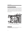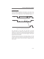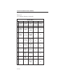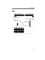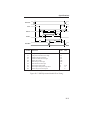
1
ZT 8832 I/O Control Processor OPERATING MANUAL For ZT 8832 Revision 0.5 and ZT 88CT32 Revision 0.4 Reorder Part Number ZT M8832 May 10, 1994 1050 Southwood Drive San Luis Obispo, CA 93401 USA FAX (805) 541-5088 Telephone (805) 541-0488 ZIATECH 5+5 WARRANTY For Ziatech Board- and System-Level Computer Products FIVE-YEAR LIMITED WARRANTY Products manufactured by Ziatech Corporation are covered from the date of purchase by a five-year warranty against defects in materials, workmanship, and published specifications applicable to the date of manufacture. During the warranty period, Ziatech will repair or replace, solely at its option, defective units provided they are returned at customer expense to an authorized Ziatech repair facility. Products which have been subjected to misuse, abuse, neglect, alteration, or unauthorized repair, determined at the sole discretion of Ziatech, whether by accident or otherwise, are excluded from warranty. The warranty on fans and disk drives is limited to two years and the warranty on flat panel displays is limited to nine months from date of purchase. Other products and accessories not manufactured by Ziatech are limited to the warranty provided by the original manufacturer. Consumable items (fuses, batteries, etc.) and software are not covered by this warranty. Within 90 days of shipping date, Ziatech will replace software disk media should it prove defective. Ziatech may offer, where applicable and available, replacement products; otherwise, repairs requiring components, assemblies, and other purchased materials may be limited by market availability. Ziatech assumes no liability resulting from changes to government regulations affecting use of materials, equipment, safety, and methods of repair. Ziatech may, at its discretion, offer replacement products. THE ABOVE WARRANTY IS IN LIEU OF ANY OTHER WARRANTY, WHETHER EXPRESSED, IMPLIED, OR STATUTORY, INCLUDING, BUT NOT LIMITED TO, ANY WARRANTY FOR FITNESS OF PURPOSE, MERCHANTABILITY, OR FREEDOM FROM INFRINGEMENT OR THE LIKE, AND ANY WARRANTY OTHERWISE ARISING OUT OF ANY PROPOSAL, SPECIFICATIONS, OR SAMPLE. Ziatech neither assumes nor authorizes any person to assume for it any other liability. The liability of Ziatech under this warranty agreement is limited to a refund of the purchase price. In no event shall Ziatech be liable for loss of profits, use, incidental, consequential, or other damage, under this agreement. SPECIAL EXTENDED WARRANTY OPTION In addition to the standard five-year warranty, Ziatech offers, for a nominal fee, an extended period of warranty up to five extra years. This extended warranty period provides similar coverage and conditions as stated above in the five-year limited warranty agreement. LIFE SUPPORT POLICY Ziatech products are not authorized for use as critical components in life support devices or systems without the express written approval of the president of Ziatech Corporation. As used herein: 1. Life support devices or systems are devices or systems which support or sustain life, and whose failure to perform, when properly used in accordance with instructions for use provided in the labeling, can be reasonably expected to result in a significant injury to the user. 2. A critical component is any component of a life support device or system whose failure to perform can be expected to cause the failure of the life support device or system, affect its safety, or limit its effectiveness. 1998 Ziatech Corporation Turbo Debugger is a registered trademark of Borland International, Inc. IBM PC/XT/AT and PC DOS are registered trademarks of International Business Machines, Inc. MULTIMODULE is a trademark of Intel Corporation. DEBUG/RT is a trademark of Paradigm Systems. CUSTOMER SUPPORT If you have a technical question, please call Ziatech’s Customer Support Service at the following number: Corporate Headquarters: (805) 541-0488 (805) 541-5088 (FAX) You can also use a modem to leave a message on the 24-hour Ziatech Bulletin Board Service (BBS) by calling (805) 541-8218. The BBS will also provide you with current Ziatech product revision and upgrade information. If you have a sales question, please contact your local Ziatech Sales Representative. PREFACE This manual describes the operation and use of the ZT 8832 and the ZT 88CT32. The boards are functionally identical. However, the ZT 88CT32 consumes less power and operates over a wider temperature range. Refer to Appendix B for actual specifications. The term ZT 8832 is used throughout the manual to reference both products, except where otherwise noted. The following organizational outline describes the focus of each chapter in this manual. Section headings enclosed in boxes indicate the locations of labeled tabs for quick access to the appropriate information. I. INTRODUCTION Chapter 1, "Introduction," offers an overview of the ZT 8832. It includes a product definition, a list of product features, a functional block diagram, and a brief description of each block. This chapter is most useful to those comparing the features of the ZT 8832 against the needs of a specific application. II. GETTING STARTED Chapter 2, "Getting Started," summarizes the information essential to getting your ZT 8832 operational. This includes system requirements, memory and I/O mapping, and a brief description of the jumper options. In many cases this information is all that is needed to begin using the ZT 8832. The section entitled "USER’S REFERENCE" includes more detailed discussions of the topics presented in this chapter. Preface III. USER’S REFERENCE Chapter 3, "Theory Of Operation," presents a detailed description of ZT 8832 system level operation. Topics discussed include commonly asked questions, memory and I/O organization, and interrupt structure. Chapter 4, "Application Examples," gives specific examples of the ZT 8832 in operation, including code to implement these applications. Chapter 5, "Processor Description (V40)," divides the V40 into functional blocks and presents a theory of operation for each. This chapter is most useful to those not familiar with the architecture of the V40/8088 series microprocessor. Chapter 6, "Processor Configuration (V40)," describes the architecture of a V40 software programmable register set used to configure peripherals resident on the V40 for specific applications. These peripherals are described in detail in the following chapters. Chapter 7, "Counter/Timers (V40)," describes the function, configuration, and operation of the V40 Counter/Timer Control Unit, which includes three 16-bit counter/timers and is functionally equivalent to the 8254 Programmable Interval Timer. The chapter also includes register descriptions. Chapter 8, "Interrupt Controller (V40)," describes the function, configuration, and operation of the V40 Interrupt Control Unit, a programmable interface between interrupt-generating peripherals and the CPU. The chapter also includes register descriptions. Preface Chapter 9, "DMA Controller (V40)," describes the function, configuration, and operation of the V40 Direct Memory Access Control Unit, a programmable peripheral device used to direct high speed data transfers between the ZT 8832 and SBX expansion module I/O. The chapter also includes register descriptions. Chapter 10, "Serial Communications (V40)," describes the function, configuration, and operation of the V40 Serial Control Unit, a single serial channel that performs asynchronous serial communication between the V40 and a serial device external to the ZT 8832. The chapter also includes register descriptions. Chapter 11, "Serial Communications (82050)," describes the function, configuration, and operation of the serial controller external to the V40. This is the Intel 82050 Asynchronous Communications Controller, or equivalent. The chapter also includes register descriptions. Chapter 12, "Parallel I/O," describes the function, configuration, and operation of the ZT 8832 parallel I/O. Parallel I/O is used to control industry standard I/O modules, such as those manufactured by Opto 22, Gordos, Crydom, and Adtek. The on-board programmable LEDs are also controlled through parallel I/O. Chapter 13, "Watchdog Timer," describes the function, configuration, and operation of the ZT 8832 two-stage watchdog timer, which is used to monitor ZT 8832 operation and take corrective action if the ZT 8832 fails to function as programmed. Chapter 14, "SBX Expansion Module," contains a description and installation information for the optional SBX expansion module, which can be used to expand the I/O capabilities of the ZT 8832. Preface Chapter 15, "Numeric Data Processor (8087)," explains installation and operation of the optional 8087 Numeric Data Processor, used to enhance the math capabilities of the ZT 8832 for numerically intensive applications. IV. APPENDICES Appendix A, "Jumper Selections," provides a detailed explanation of the ZT 8832 options that are selectable through jumper configuration or the use of cuttable traces. Appendix B, "Specifications," contains the electrical, environmental, and mechanical specifications for the ZT 8832. Frontplane connector pinouts, cable drawings, and timing diagrams are also included. Appendix C, "Customer Support," offers a product revision history, technical support information, and instructions for returning the ZT 8832 for service. Appendix D, "Glossary," defines important terms and acronyms used throughout the manual. CONTENTS I. INTRODUCTION Chapter 1. INTRODUCTION 1-1 OVERVIEW . . . . . . . . . . . . . . . . . . . . . . . . . . . . . . . . . . . . . . . . . . . . . . . . . . . . . 1-2 Product Definition . . . . . . . . . . . . . . . . . . . . . . . . . . . . . . . . . . . . . . . . . . . . 1-2 Features of the ZT 8832 . . . . . . . . . . . . . . . . . . . . . . . . . . . . . . . . . . . . . . . 1-3 Development Considerations . . . . . . . . . . . . . . . . . . . . . . . . . . . . . . . . . . . 1-4 FUNCTIONAL BLOCKS . . . . . . . . . . . . . . . . . . . . . . . . . . . . . . . . . . . . . . . . . 1-6 V40 (µPD70208) Processor . . . . . . . . . . . . . . . . . . . . . . . . . . . . . . . . . . . . 1-6 Local Memory . . . . . . . . . . . . . . . . . . . . . . . . . . . . . . . . . . . . . . . . . . . . . . . 1-6 Dual Port Memory . . . . . . . . . . . . . . . . . . . . . . . . . . . . . . . . . . . . . . . . . . . . 1-7 Board Select Option . . . . . . . . . . . . . . . . . . . . . . . . . . . . . . . . . . . . . . . . . . 1-7 Serial Communications . . . . . . . . . . . . . . . . . . . . . . . . . . . . . . . . . . . . . . . 1-8 Parallel Input/Output . . . . . . . . . . . . . . . . . . . . . . . . . . . . . . . . . . . . . . . . . . 1-8 Interrupt Controller . . . . . . . . . . . . . . . . . . . . . . . . . . . . . . . . . . . . . . . . . . . 1-9 Counter/Timers . . . . . . . . . . . . . . . . . . . . . . . . . . . . . . . . . . . . . . . . . . . . . . 1-9 Watchdog Timer . . . . . . . . . . . . . . . . . . . . . . . . . . . . . . . . . . . . . . . . . . . . . . 1-9 zSBX Expansion Module Socket . . . . . . . . . . . . . . . . . . . . . . . . . . . . . . 1-10 Numeric Data Processor Socket . . . . . . . . . . . . . . . . . . . . . . . . . . . . . . . 1-10 II. GETTING STARTED Chapter 2. GETTING STARTED OVERVIEW . . . . . . . . . . . . . . . . . . . . . . . . . . . . . . . . . . . . . . . . . . . . . . . . . . . . . UNPACKING . . . . . . . . . . . . . . . . . . . . . . . . . . . . . . . . . . . . . . . . . . . . . . . . . . . . WHAT’S IN THE BOX? . . . . . . . . . . . . . . . . . . . . . . . . . . . . . . . . . . . . . . . . . . SYSTEM REQUIREMENTS . . . . . . . . . . . . . . . . . . . . . . . . . . . . . . . . . . . . . . ZT 8832 Requirements . . . . . . . . . . . . . . . . . . . . . . . . . . . . . . . . . . . . . . . . 2-1 2-1 2-2 2-2 2-3 2-3 Contents ZT 88CT32 Requirements . . . . . . . . . . . . . . . . . . . . . . . . . . . . . . . . . . . . . 2-3 INSTALLING THE ZT 8832 WITH STD ROM . . . . . . . . . . . . . . . . . . . . . 2-5 Memory Requirements . . . . . . . . . . . . . . . . . . . . . . . . . . . . . . . . . . . . . . . . 2-5 Cable Requirements . . . . . . . . . . . . . . . . . . . . . . . . . . . . . . . . . . . . . . . . . . 2-5 Jumper Requirements . . . . . . . . . . . . . . . . . . . . . . . . . . . . . . . . . . . . . . . . . 2-6 Operation . . . . . . . . . . . . . . . . . . . . . . . . . . . . . . . . . . . . . . . . . . . . . . . . . . . . 2-6 INSTALLING THE ZT 8832 WITH DOS MPX . . . . . . . . . . . . . . . . . . . . . 2-7 Memory Requirements . . . . . . . . . . . . . . . . . . . . . . . . . . . . . . . . . . . . . . . . 2-7 Cable Requirements . . . . . . . . . . . . . . . . . . . . . . . . . . . . . . . . . . . . . . . . . . 2-7 Jumper Requirements . . . . . . . . . . . . . . . . . . . . . . . . . . . . . . . . . . . . . . . . . 2-8 Operation . . . . . . . . . . . . . . . . . . . . . . . . . . . . . . . . . . . . . . . . . . . . . . . . . . . . 2-8 MEMORY . . . . . . . . . . . . . . . . . . . . . . . . . . . . . . . . . . . . . . . . . . . . . . . . . . . . . 2-10 I/O . . . . . . . . . . . . . . . . . . . . . . . . . . . . . . . . . . . . . . . . . . . . . . . . . . . . . . . . . . . . 2-12 JUMPER OPTIONS . . . . . . . . . . . . . . . . . . . . . . . . . . . . . . . . . . . . . . . . . . . . . 2-14 III. USER’S REFERENCE Chapter 3. THEORY OF OPERATION 3-1 OVERVIEW . . . . . . . . . . . . . . . . . . . . . . . . . . . . . . . . . . . . . . . . . . . . . . . . . . . . . 3-2 COMMONLY ASKED QUESTIONS . . . . . . . . . . . . . . . . . . . . . . . . . . . . . . 3-3 DUAL PORT MEMORY . . . . . . . . . . . . . . . . . . . . . . . . . . . . . . . . . . . . . . . . . . 3-8 STD BUS AND LOCAL CONTROL PORTS . . . . . . . . . . . . . . . . . . . . . . . 3-9 STD Bus Control Port Overview . . . . . . . . . . . . . . . . . . . . . . . . . . . . . . . 3-9 STD Bus Control Port Architecture . . . . . . . . . . . . . . . . . . . . . . . . . . . . 3-10 Local Control Port Overview . . . . . . . . . . . . . . . . . . . . . . . . . . . . . . . . . 3-12 Local Control Port Architecture . . . . . . . . . . . . . . . . . . . . . . . . . . . . . . . 3-13 BOARD SELECT OPTION . . . . . . . . . . . . . . . . . . . . . . . . . . . . . . . . . . . . . . 3-15 STD BUS INTERRUPTS . . . . . . . . . . . . . . . . . . . . . . . . . . . . . . . . . . . . . . . . 3-17 RESET . . . . . . . . . . . . . . . . . . . . . . . . . . . . . . . . . . . . . . . . . . . . . . . . . . . . . . . . . 3-21 Chapter 4. APPLICATION EXAMPLES 4-1 OVERVIEW . . . . . . . . . . . . . . . . . . . . . . . . . . . . . . . . . . . . . . . . . . . . . . . . . . . . . 4-1 EXAMPLE 1: V40 INITIALIZATION . . . . . . . . . . . . . . . . . . . . . . . . . . . . . . 4-2 Objectives . . . . . . . . . . . . . . . . . . . . . . . . . . . . . . . . . . . . . . . . . . . . . . . . . . . 4-2 Program Code . . . . . . . . . . . . . . . . . . . . . . . . . . . . . . . . . . . . . . . . . . . . . . . . 4-3 EXAMPLE 2: PERIPHERAL INITIALIZATION . . . . . . . . . . . . . . . . . . . . 4-6 Objectives . . . . . . . . . . . . . . . . . . . . . . . . . . . . . . . . . . . . . . . . . . . . . . . . . . . 4-6 Program Code . . . . . . . . . . . . . . . . . . . . . . . . . . . . . . . . . . . . . . . . . . . . . . . . 4-6 EXAMPLE 3: WATCHDOG TIMER . . . . . . . . . . . . . . . . . . . . . . . . . . . . . . 4-18 Contents Objectives . . . . . . . . . . . . . . . . . . . . . . . . . . . . . . . . . . . . . . . . . . . . . . . . . . 4-18 Program Code . . . . . . . . . . . . . . . . . . . . . . . . . . . . . . . . . . . . . . . . . . . . . . 4-19 Chapter 5. PROCESSOR DESCRIPTION (V40) 5-1 OVERVIEW . . . . . . . . . . . . . . . . . . . . . . . . . . . . . . . . . . . . . . . . . . . . . . . . . . . . . 5-2 ZT 8832 SPECIFICS . . . . . . . . . . . . . . . . . . . . . . . . . . . . . . . . . . . . . . . . . . . . . 5-2 COMMONLY ASKED QUESTIONS . . . . . . . . . . . . . . . . . . . . . . . . . . . . . . 5-3 FUNCTIONAL BLOCKS . . . . . . . . . . . . . . . . . . . . . . . . . . . . . . . . . . . . . . . . . 5-5 CPU - Central Processing Unit . . . . . . . . . . . . . . . . . . . . . . . . . . . . . . . . . 5-6 BIU - Bus Interface Unit . . . . . . . . . . . . . . . . . . . . . . . . . . . . . . . . . . . . . 5-19 BAU - Bus Arbitration Unit . . . . . . . . . . . . . . . . . . . . . . . . . . . . . . . . . . 5-19 CGU - Clock Generator Unit . . . . . . . . . . . . . . . . . . . . . . . . . . . . . . . . . 5-20 VCR - V40 Configuration Registers . . . . . . . . . . . . . . . . . . . . . . . . . . . 5-20 WCU - Wait Control Unit . . . . . . . . . . . . . . . . . . . . . . . . . . . . . . . . . . . . 5-21 SCU - Serial Control Unit . . . . . . . . . . . . . . . . . . . . . . . . . . . . . . . . . . . . 5-21 TCU - Counter/Timer Control Unit . . . . . . . . . . . . . . . . . . . . . . . . . . . . 5-21 ICU - Interrupt Control Unit . . . . . . . . . . . . . . . . . . . . . . . . . . . . . . . . . . 5-22 DCU - DMA Control Unit . . . . . . . . . . . . . . . . . . . . . . . . . . . . . . . . . . . . 5-22 RESET . . . . . . . . . . . . . . . . . . . . . . . . . . . . . . . . . . . . . . . . . . . . . . . . . . . . . . . . . 5-23 MEMORY AND I/O ADDRESSING . . . . . . . . . . . . . . . . . . . . . . . . . . . . . . 5-24 INTERRUPTS . . . . . . . . . . . . . . . . . . . . . . . . . . . . . . . . . . . . . . . . . . . . . . . . . . 5-27 Divide Error . . . . . . . . . . . . . . . . . . . . . . . . . . . . . . . . . . . . . . . . . . . . . . . . 5-31 Single-Step . . . . . . . . . . . . . . . . . . . . . . . . . . . . . . . . . . . . . . . . . . . . . . . . . 5-31 Non-Maskable . . . . . . . . . . . . . . . . . . . . . . . . . . . . . . . . . . . . . . . . . . . . . . 5-32 Fixed Vector Instruction . . . . . . . . . . . . . . . . . . . . . . . . . . . . . . . . . . . . . . 5-32 Overflow . . . . . . . . . . . . . . . . . . . . . . . . . . . . . . . . . . . . . . . . . . . . . . . . . . . 5-32 Check Index . . . . . . . . . . . . . . . . . . . . . . . . . . . . . . . . . . . . . . . . . . . . . . . . 5-33 Variable Vector Instruction . . . . . . . . . . . . . . . . . . . . . . . . . . . . . . . . . . . 5-33 Emulation Mode . . . . . . . . . . . . . . . . . . . . . . . . . . . . . . . . . . . . . . . . . . . . 5-33 8080 EMULATION . . . . . . . . . . . . . . . . . . . . . . . . . . . . . . . . . . . . . . . . . . . . . 5-34 Chapter 6. PROCESSOR CONFIGURATION (V40) 6-1 OVERVIEW . . . . . . . . . . . . . . . . . . . . . . . . . . . . . . . . . . . . . . . . . . . . . . . . . . . . . 6-1 VCR - V40 CONFIGURATION REGISTERS . . . . . . . . . . . . . . . . . . . . . . . 6-2 OPCN - On Chip Peripheral Connection Register . . . . . . . . . . . . . . . . 6-3 OPSEL - On Chip Peripheral Selection Register . . . . . . . . . . . . . . . . . 6-4 OPHA, DULA, IULA, TULA, and SULA . . . . . . . . . . . . . . . . . . . . . . . 6-5 WCY2 - Wait Cycle 2 Register . . . . . . . . . . . . . . . . . . . . . . . . . . . . . . . . . 6-7 WCY1 - Wait Cycle 1 Register . . . . . . . . . . . . . . . . . . . . . . . . . . . . . . . . . 6-7 WMB - Wait Memory Boundary Register . . . . . . . . . . . . . . . . . . . . . . . 6-9 RFC - Refresh Control Register . . . . . . . . . . . . . . . . . . . . . . . . . . . . . . . 6-10 Contents TCKS - Counter/Timer Clock Selection Register . . . . . . . . . . . . . . . . 6-10 RESET . . . . . . . . . . . . . . . . . . . . . . . . . . . . . . . . . . . . . . . . . . . . . . . . . . . . . . . . . 6-12 Chapter 7. COUNTER/TIMERS (V40) 7-1 OVERVIEW . . . . . . . . . . . . . . . . . . . . . . . . . . . . . . . . . . . . . . . . . . . . . . . . . . . . . 7-2 ZT 8832 SPECIFICS . . . . . . . . . . . . . . . . . . . . . . . . . . . . . . . . . . . . . . . . . . . . . 7-3 FUNCTIONAL DESCRIPTION . . . . . . . . . . . . . . . . . . . . . . . . . . . . . . . . . . . 7-4 Read/Write Control . . . . . . . . . . . . . . . . . . . . . . . . . . . . . . . . . . . . . . . . . . . 7-4 Mode Register . . . . . . . . . . . . . . . . . . . . . . . . . . . . . . . . . . . . . . . . . . . . . . . 7-5 Clock Select and Divisor . . . . . . . . . . . . . . . . . . . . . . . . . . . . . . . . . . . . . . 7-5 Counter/Timers 0, 1, and 2 . . . . . . . . . . . . . . . . . . . . . . . . . . . . . . . . . . . . 7-5 PROGRAMMABLE REGISTERS . . . . . . . . . . . . . . . . . . . . . . . . . . . . . . . . . 7-7 Timer Mode Register (TMD) . . . . . . . . . . . . . . . . . . . . . . . . . . . . . . . . . . 7-8 Count Registers . . . . . . . . . . . . . . . . . . . . . . . . . . . . . . . . . . . . . . . . . . . . . 7-12 Status Registers . . . . . . . . . . . . . . . . . . . . . . . . . . . . . . . . . . . . . . . . . . . . . 7-12 OPERATION . . . . . . . . . . . . . . . . . . . . . . . . . . . . . . . . . . . . . . . . . . . . . . . . . . . 7-14 Reset . . . . . . . . . . . . . . . . . . . . . . . . . . . . . . . . . . . . . . . . . . . . . . . . . . . . . . 7-14 Count Latch Command . . . . . . . . . . . . . . . . . . . . . . . . . . . . . . . . . . . . . . 7-14 Multiple Latch Command . . . . . . . . . . . . . . . . . . . . . . . . . . . . . . . . . . . . 7-15 Modes of Operation . . . . . . . . . . . . . . . . . . . . . . . . . . . . . . . . . . . . . . . . . 7-16 Programming . . . . . . . . . . . . . . . . . . . . . . . . . . . . . . . . . . . . . . . . . . . . . . . 7-28 Chapter 8. INTERRUPT CONTROLLER (V40) 8-1 OVERVIEW . . . . . . . . . . . . . . . . . . . . . . . . . . . . . . . . . . . . . . . . . . . . . . . . . . . . . 8-2 ZT 8832 SPECIFICS . . . . . . . . . . . . . . . . . . . . . . . . . . . . . . . . . . . . . . . . . . . . . 8-3 FUNCTIONAL DESCRIPTION . . . . . . . . . . . . . . . . . . . . . . . . . . . . . . . . . . . 8-4 Interrupt Request Register . . . . . . . . . . . . . . . . . . . . . . . . . . . . . . . . . . . . . 8-4 Interrupt Mask Register . . . . . . . . . . . . . . . . . . . . . . . . . . . . . . . . . . . . . . . 8-5 Priority Resolver . . . . . . . . . . . . . . . . . . . . . . . . . . . . . . . . . . . . . . . . . . . . . 8-5 Interrupt In-Service Register . . . . . . . . . . . . . . . . . . . . . . . . . . . . . . . . . . . 8-5 Control Logic . . . . . . . . . . . . . . . . . . . . . . . . . . . . . . . . . . . . . . . . . . . . . . . . 8-6 Read/Write Control Logic . . . . . . . . . . . . . . . . . . . . . . . . . . . . . . . . . . . . . 8-6 Initialization and Operation Registers . . . . . . . . . . . . . . . . . . . . . . . . . . . 8-6 PROGRAMMABLE REGISTERS . . . . . . . . . . . . . . . . . . . . . . . . . . . . . . . . . 8-7 Initialization Words (IIW1, IIW2, IIW3, and IIW4) . . . . . . . . . . . . . . . 8-8 Operation Words (IMKW, IPFW, and IMDW) . . . . . . . . . . . . . . . . . . 8-12 Status Words (IRQ, IIS, and IPOL) . . . . . . . . . . . . . . . . . . . . . . . . . . . . 8-16 OPERATION . . . . . . . . . . . . . . . . . . . . . . . . . . . . . . . . . . . . . . . . . . . . . . . . . . . 8-19 Reset . . . . . . . . . . . . . . . . . . . . . . . . . . . . . . . . . . . . . . . . . . . . . . . . . . . . . . 8-19 Interrupts . . . . . . . . . . . . . . . . . . . . . . . . . . . . . . . . . . . . . . . . . . . . . . . . . . . 8-19 Interrupt Vectors . . . . . . . . . . . . . . . . . . . . . . . . . . . . . . . . . . . . . . . . . . . . 8-21 Contents Interrupt Nesting . . . . . . . . . . . . . . . . . . . . . . . . . . . . . . . . . . . . . . . . . . . . Level- or Edge-Triggered . . . . . . . . . . . . . . . . . . . . . . . . . . . . . . . . . . . . Finish Interrupts . . . . . . . . . . . . . . . . . . . . . . . . . . . . . . . . . . . . . . . . . . . . . Automatic Priority Rotation . . . . . . . . . . . . . . . . . . . . . . . . . . . . . . . . . . Specific Priority Rotation . . . . . . . . . . . . . . . . . . . . . . . . . . . . . . . . . . . . Interrupt Masking . . . . . . . . . . . . . . . . . . . . . . . . . . . . . . . . . . . . . . . . . . . Interrupt Status . . . . . . . . . . . . . . . . . . . . . . . . . . . . . . . . . . . . . . . . . . . . . . Programming . . . . . . . . . . . . . . . . . . . . . . . . . . . . . . . . . . . . . . . . . . . . . . . 8-22 8-25 8-26 8-28 8-29 8-30 8-31 8-31 Chapter 9. DMA CONTROLLER (V40) 9-1 OVERVIEW . . . . . . . . . . . . . . . . . . . . . . . . . . . . . . . . . . . . . . . . . . . . . . . . . . . . . 9-2 ZT 8832 SPECIFICS . . . . . . . . . . . . . . . . . . . . . . . . . . . . . . . . . . . . . . . . . . . . . 9-3 FUNCTIONAL DESCRIPTION . . . . . . . . . . . . . . . . . . . . . . . . . . . . . . . . . . . 9-4 Internal Bus Interface . . . . . . . . . . . . . . . . . . . . . . . . . . . . . . . . . . . . . . . . . 9-5 Address Register . . . . . . . . . . . . . . . . . . . . . . . . . . . . . . . . . . . . . . . . . . . . . 9-5 Address Adjuster . . . . . . . . . . . . . . . . . . . . . . . . . . . . . . . . . . . . . . . . . . . . . 9-5 Count Register . . . . . . . . . . . . . . . . . . . . . . . . . . . . . . . . . . . . . . . . . . . . . . . 9-6 Count Adjuster . . . . . . . . . . . . . . . . . . . . . . . . . . . . . . . . . . . . . . . . . . . . . . . 9-6 Control Registers . . . . . . . . . . . . . . . . . . . . . . . . . . . . . . . . . . . . . . . . . . . . . 9-6 PROGRAMMABLE REGISTERS . . . . . . . . . . . . . . . . . . . . . . . . . . . . . . . . . 9-7 DMA Initialize Command (DICM) . . . . . . . . . . . . . . . . . . . . . . . . . . . . . 9-8 DMA Channel (DCH) . . . . . . . . . . . . . . . . . . . . . . . . . . . . . . . . . . . . . . . . 9-8 DMA Base Count/Current Count (DBC/DCC) . . . . . . . . . . . . . . . . . . 9-10 DMA Base Address/Current Address (DBA/DCA) . . . . . . . . . . . . . . 9-11 DMA Device Control (DDC) . . . . . . . . . . . . . . . . . . . . . . . . . . . . . . . . . 9-12 DMA Mode (DMD) . . . . . . . . . . . . . . . . . . . . . . . . . . . . . . . . . . . . . . . . . 9-13 DMA Status (DST) . . . . . . . . . . . . . . . . . . . . . . . . . . . . . . . . . . . . . . . . . . 9-15 DMA Mask (DMK) . . . . . . . . . . . . . . . . . . . . . . . . . . . . . . . . . . . . . . . . . 9-16 OPERATION . . . . . . . . . . . . . . . . . . . . . . . . . . . . . . . . . . . . . . . . . . . . . . . . . . . 9-17 Reset . . . . . . . . . . . . . . . . . . . . . . . . . . . . . . . . . . . . . . . . . . . . . . . . . . . . . . 9-17 Autoinitialization . . . . . . . . . . . . . . . . . . . . . . . . . . . . . . . . . . . . . . . . . . . . 9-18 Programming . . . . . . . . . . . . . . . . . . . . . . . . . . . . . . . . . . . . . . . . . . . . . . . 9-18 Chapter 10. SERIAL COMMUNICATIONS (V40) OVERVIEW . . . . . . . . . . . . . . . . . . . . . . . . . . . . . . . . . . . . . . . . . . . . . . . . . . . . ZT 8832 SPECIFICS . . . . . . . . . . . . . . . . . . . . . . . . . . . . . . . . . . . . . . . . . . . . FUNCTIONAL DESCRIPTION . . . . . . . . . . . . . . . . . . . . . . . . . . . . . . . . . . Read/Write Control . . . . . . . . . . . . . . . . . . . . . . . . . . . . . . . . . . . . . . . . . . Receiver . . . . . . . . . . . . . . . . . . . . . . . . . . . . . . . . . . . . . . . . . . . . . . . . . . . Transmitter . . . . . . . . . . . . . . . . . . . . . . . . . . . . . . . . . . . . . . . . . . . . . . . . . Interrupt Generation Logic . . . . . . . . . . . . . . . . . . . . . . . . . . . . . . . . . . . 10-1 10-2 10-2 10-3 10-4 10-4 10-4 10-4 Contents PROGRAMMABLE REGISTERS . . . . . . . . . . . . . . . . . . . . . . . . . . . . . . . . 10-5 Serial Status Register (SST) . . . . . . . . . . . . . . . . . . . . . . . . . . . . . . . . . . 10-6 Serial Command Register (SCM) . . . . . . . . . . . . . . . . . . . . . . . . . . . . . 10-8 Serial Mode Register (SMD) . . . . . . . . . . . . . . . . . . . . . . . . . . . . . . . . . 10-9 Serial Interrupt Mask Register (SIMK) . . . . . . . . . . . . . . . . . . . . . . . 10-10 OPERATION . . . . . . . . . . . . . . . . . . . . . . . . . . . . . . . . . . . . . . . . . . . . . . . . . . 10-11 Reset . . . . . . . . . . . . . . . . . . . . . . . . . . . . . . . . . . . . . . . . . . . . . . . . . . . . . 10-11 Serial Data Format . . . . . . . . . . . . . . . . . . . . . . . . . . . . . . . . . . . . . . . . . 10-12 Baud Rate . . . . . . . . . . . . . . . . . . . . . . . . . . . . . . . . . . . . . . . . . . . . . . . . . 10-13 Interrupt and Polled Communication . . . . . . . . . . . . . . . . . . . . . . . . . 10-15 Programming . . . . . . . . . . . . . . . . . . . . . . . . . . . . . . . . . . . . . . . . . . . . . . 10-16 Chapter 11. SERIAL COMMUNICATIONS (82050) 11-1 OVERVIEW . . . . . . . . . . . . . . . . . . . . . . . . . . . . . . . . . . . . . . . . . . . . . . . . . . . . 11-2 ZT 8832 SPECIFICS . . . . . . . . . . . . . . . . . . . . . . . . . . . . . . . . . . . . . . . . . . . . 11-3 FUNCTIONAL DESCRIPTION . . . . . . . . . . . . . . . . . . . . . . . . . . . . . . . . . . 11-4 Read/Write Control . . . . . . . . . . . . . . . . . . . . . . . . . . . . . . . . . . . . . . . . . . 11-5 Receiver . . . . . . . . . . . . . . . . . . . . . . . . . . . . . . . . . . . . . . . . . . . . . . . . . . . . 11-5 Transmitter . . . . . . . . . . . . . . . . . . . . . . . . . . . . . . . . . . . . . . . . . . . . . . . . . 11-5 Modem Control . . . . . . . . . . . . . . . . . . . . . . . . . . . . . . . . . . . . . . . . . . . . . 11-6 Interrupt Control . . . . . . . . . . . . . . . . . . . . . . . . . . . . . . . . . . . . . . . . . . . . 11-6 PROGRAMMABLE REGISTERS . . . . . . . . . . . . . . . . . . . . . . . . . . . . . . . . 11-7 Transmit and Receive Buffer . . . . . . . . . . . . . . . . . . . . . . . . . . . . . . . . . 11-8 Line Control . . . . . . . . . . . . . . . . . . . . . . . . . . . . . . . . . . . . . . . . . . . . . . . . 11-8 Line Status . . . . . . . . . . . . . . . . . . . . . . . . . . . . . . . . . . . . . . . . . . . . . . . . 11-11 Modem Control . . . . . . . . . . . . . . . . . . . . . . . . . . . . . . . . . . . . . . . . . . . . 11-13 Modem Status . . . . . . . . . . . . . . . . . . . . . . . . . . . . . . . . . . . . . . . . . . . . . 11-15 Divisor Latch . . . . . . . . . . . . . . . . . . . . . . . . . . . . . . . . . . . . . . . . . . . . . . 11-17 Interrupt Identify . . . . . . . . . . . . . . . . . . . . . . . . . . . . . . . . . . . . . . . . . . . 11-18 Interrupt Enable . . . . . . . . . . . . . . . . . . . . . . . . . . . . . . . . . . . . . . . . . . . . 11-19 OPERATION . . . . . . . . . . . . . . . . . . . . . . . . . . . . . . . . . . . . . . . . . . . . . . . . . . 11-20 Reset . . . . . . . . . . . . . . . . . . . . . . . . . . . . . . . . . . . . . . . . . . . . . . . . . . . . . 11-20 Serial Data Format . . . . . . . . . . . . . . . . . . . . . . . . . . . . . . . . . . . . . . . . . 11-21 Baud Rate . . . . . . . . . . . . . . . . . . . . . . . . . . . . . . . . . . . . . . . . . . . . . . . . . 11-22 Interrupt and Polled Communication . . . . . . . . . . . . . . . . . . . . . . . . . . 11-23 RS-485 Serial Communications . . . . . . . . . . . . . . . . . . . . . . . . . . . . . . 11-23 Programming . . . . . . . . . . . . . . . . . . . . . . . . . . . . . . . . . . . . . . . . . . . . . . 11-24 Contents Chapter 12. PARALLEL I/O OVERVIEW . . . . . . . . . . . . . . . . . . . . . . . . . . . . . . . . . . . . . . . . . . . . . . . . . . . . ZT 8832 SPECIFICS . . . . . . . . . . . . . . . . . . . . . . . . . . . . . . . . . . . . . . . . . . . . FUNCTIONAL DESCRIPTION . . . . . . . . . . . . . . . . . . . . . . . . . . . . . . . . . . Output Latch . . . . . . . . . . . . . . . . . . . . . . . . . . . . . . . . . . . . . . . . . . . . . . . . Output Buffer . . . . . . . . . . . . . . . . . . . . . . . . . . . . . . . . . . . . . . . . . . . . . . . Input Buffer . . . . . . . . . . . . . . . . . . . . . . . . . . . . . . . . . . . . . . . . . . . . . . . . PROGRAMMABLE REGISTERS . . . . . . . . . . . . . . . . . . . . . . . . . . . . . . . . OPERATION . . . . . . . . . . . . . . . . . . . . . . . . . . . . . . . . . . . . . . . . . . . . . . . . . . . Reset . . . . . . . . . . . . . . . . . . . . . . . . . . . . . . . . . . . . . . . . . . . . . . . . . . . . . . Programming the Parallel Ports . . . . . . . . . . . . . . . . . . . . . . . . . . . . . . . Programming the Light Emitting Diode . . . . . . . . . . . . . . . . . . . . . . . . Mixing I/O in a Single Port . . . . . . . . . . . . . . . . . . . . . . . . . . . . . . . . . . . 12-1 12-1 12-2 12-3 12-3 12-4 12-4 12-5 12-6 12-6 12-6 12-7 12-7 Chapter 13. WATCHDOG TIMER OVERVIEW . . . . . . . . . . . . . . . . . . . . . . . . . . . . . . . . . . . . . . . . . . . . . . . . . . . . ZT 8832 SPECIFICS . . . . . . . . . . . . . . . . . . . . . . . . . . . . . . . . . . . . . . . . . . . . FUNCTIONAL DESCRIPTION . . . . . . . . . . . . . . . . . . . . . . . . . . . . . . . . . . Stage 1 Timer . . . . . . . . . . . . . . . . . . . . . . . . . . . . . . . . . . . . . . . . . . . . . . . Stage 1 Delay . . . . . . . . . . . . . . . . . . . . . . . . . . . . . . . . . . . . . . . . . . . . . . . Stage 2 Timer . . . . . . . . . . . . . . . . . . . . . . . . . . . . . . . . . . . . . . . . . . . . . . . Stage 2 Delay . . . . . . . . . . . . . . . . . . . . . . . . . . . . . . . . . . . . . . . . . . . . . . . OPERATION . . . . . . . . . . . . . . . . . . . . . . . . . . . . . . . . . . . . . . . . . . . . . . . . . . . Reset . . . . . . . . . . . . . . . . . . . . . . . . . . . . . . . . . . . . . . . . . . . . . . . . . . . . . . Multiple Stages . . . . . . . . . . . . . . . . . . . . . . . . . . . . . . . . . . . . . . . . . . . . . Changing Time Delays . . . . . . . . . . . . . . . . . . . . . . . . . . . . . . . . . . . . . . . Programming . . . . . . . . . . . . . . . . . . . . . . . . . . . . . . . . . . . . . . . . . . . . . . . 13-1 13-2 13-2 13-3 13-3 13-4 13-4 13-4 13-5 13-5 13-6 13-7 13-8 Chapter 14. SBX EXPANSION MODULE OVERVIEW . . . . . . . . . . . . . . . . . . . . . . . . . . . . . . . . . . . . . . . . . . . . . . . . . . . . Features . . . . . . . . . . . . . . . . . . . . . . . . . . . . . . . . . . . . . . . . . . . . . . . . . . . . ZT 8832 SPECIFICS . . . . . . . . . . . . . . . . . . . . . . . . . . . . . . . . . . . . . . . . . . . . INSTALLATION . . . . . . . . . . . . . . . . . . . . . . . . . . . . . . . . . . . . . . . . . . . . . . . 14-1 14-2 14-3 14-4 14-5 Chapter 15. NUMERIC DATA PROCESSOR (8087) OVERVIEW . . . . . . . . . . . . . . . . . . . . . . . . . . . . . . . . . . . . . . . . . . . . . . . . . . . . ZT 8832 SPECIFICS . . . . . . . . . . . . . . . . . . . . . . . . . . . . . . . . . . . . . . . . . . . . INSTALLATION . . . . . . . . . . . . . . . . . . . . . . . . . . . . . . . . . . . . . . . . . . . . . . . OPERATION . . . . . . . . . . . . . . . . . . . . . . . . . . . . . . . . . . . . . . . . . . . . . . . . . . . Coprocessor Interface . . . . . . . . . . . . . . . . . . . . . . . . . . . . . . . . . . . . . . . . Error Handling and Interrupts . . . . . . . . . . . . . . . . . . . . . . . . . . . . . . . . . 15-1 15-2 15-2 15-3 15-4 15-4 15-6 Contents Further Reference . . . . . . . . . . . . . . . . . . . . . . . . . . . . . . . . . . . . . . . . . . . 15-7 IV. APPENDICES Appendix A. JUMPER CONFIGURATIONS A-1 OVERVIEW . . . . . . . . . . . . . . . . . . . . . . . . . . . . . . . . . . . . . . . . . . . . . . . . . . . . A-1 JUMPER OPTIONS . . . . . . . . . . . . . . . . . . . . . . . . . . . . . . . . . . . . . . . . . . . . . A-2 CUTTABLE TRACES . . . . . . . . . . . . . . . . . . . . . . . . . . . . . . . . . . . . . . . . . . A-16 Appendix B. SPECIFICATIONS B-1 ELECTRICAL AND ENVIRONMENTAL . . . . . . . . . . . . . . . . . . . . . . . . . B-2 Absolute Maximum Ratings . . . . . . . . . . . . . . . . . . . . . . . . . . . . . . . . . . . B-2 DC Operating Characteristics . . . . . . . . . . . . . . . . . . . . . . . . . . . . . . . . . . B-2 Battery Backup Characteristics . . . . . . . . . . . . . . . . . . . . . . . . . . . . . . . . B-2 STD Bus Loading Characteristics . . . . . . . . . . . . . . . . . . . . . . . . . . . . . . B-3 MECHANICAL . . . . . . . . . . . . . . . . . . . . . . . . . . . . . . . . . . . . . . . . . . . . . . . . . B-6 Card Dimensions & Weight . . . . . . . . . . . . . . . . . . . . . . . . . . . . . . . . . . . B-6 Connectors . . . . . . . . . . . . . . . . . . . . . . . . . . . . . . . . . . . . . . . . . . . . . . . . . . B-7 Cables . . . . . . . . . . . . . . . . . . . . . . . . . . . . . . . . . . . . . . . . . . . . . . . . . . . . . B-17 TIMING . . . . . . . . . . . . . . . . . . . . . . . . . . . . . . . . . . . . . . . . . . . . . . . . . . . . . . . B-22 Appendix C. CUSTOMER SUPPORT C-1 OVERVIEW . . . . . . . . . . . . . . . . . . . . . . . . . . . . . . . . . . . . . . . . . . . . . . . . . . . . REVISION HISTORY . . . . . . . . . . . . . . . . . . . . . . . . . . . . . . . . . . . . . . . . . . . . ZT 8832 . . . . . . . . . . . . . . . . . . . . . . . . . . . . . . . . . . . . . . . . . . . . . . . . . . . . ZT 88CT32 . . . . . . . . . . . . . . . . . . . . . . . . . . . . . . . . . . . . . . . . . . . . . . . . . . TECHNICAL ASSISTANCE . . . . . . . . . . . . . . . . . . . . . . . . . . . . . . . . . . . . . RELIABILITY . . . . . . . . . . . . . . . . . . . . . . . . . . . . . . . . . . . . . . . . . . . . . . . . . . RETURNING FOR SERVICE . . . . . . . . . . . . . . . . . . . . . . . . . . . . . . . . . . . . . ZIATECH 5+5 WARRANTY . . . . . . . . . . . . . . . . . . . . . . . . . . . . . . . . . . . . . C-1 C-2 C-2 C-3 C-4 C-5 C-6 C-7 Appendix D. GLOSSARY D-1 Contents V. INDEX Index . . . . . . . . . . . . . . . . . . . . . . . . . . . . . . . . . . . . . . . . . . . . . . . . . . . . . . . . . . . . . . i TABLES Table 2–1 Table 2–2 Table 3–1 Table 5–1 Table 5–2 Table 5–3 Table 5–4 Table 5–5 Table 5–6 Table 6–1 Table 6–2 Table 6–3 Table 7–1 Table 8–1 Table 8–2 Table 9–1 Table 9–2 Table 10–1 Table 10–2 Table 10–3 Table 11–1 Table 11–2 Table 11–3 Table 11–4 Table 11–5 Table 12–1 Table 13–1 Table A–1 Table A–2 Table A–3 Table A–4 Table B–1 Table B–2 STD ROM Jumper Configuration. . . . . . . . . . . . . . . . . . . . . . 2-6 DOS MPX Jumper Configuration. . . . . . . . . . . . . . . . . . . . . . 2-8 Devices Affected by Reset. . . . . . . . . . . . . . . . . . . . . . . . . . . 3-23 Segment Registers. . . . . . . . . . . . . . . . . . . . . . . . . . . . . . . . . . . 5-9 Implied Use of General Registers. . . . . . . . . . . . . . . . . . . . . 5-11 CPU Reset State. . . . . . . . . . . . . . . . . . . . . . . . . . . . . . . . . . . . 5-23 Interrupt Sources. . . . . . . . . . . . . . . . . . . . . . . . . . . . . . . . . . . 5-28 Interrupt Vector Table. . . . . . . . . . . . . . . . . . . . . . . . . . . . . . . 5-30 Emulation Mode Registers and Flags. . . . . . . . . . . . . . . . . 5-36 V40 Configuration Registers. . . . . . . . . . . . . . . . . . . . . . . . . . 6-2 STD ROM Programmable Address Selection. . . . . . . . . . . 6-6 V40 Configuration Register Defaults. . . . . . . . . . . . . . . . . . 6-12 TCU Register Addressing. . . . . . . . . . . . . . . . . . . . . . . . . . . . . 7-7 Interrupt Controller Inputs. . . . . . . . . . . . . . . . . . . . . . . . . . . . 8-3 ICU Register Addressing. . . . . . . . . . . . . . . . . . . . . . . . . . . . . 8-7 DCU Register Addressing. . . . . . . . . . . . . . . . . . . . . . . . . . . . 9-7 DCU Register Default State. . . . . . . . . . . . . . . . . . . . . . . . . . 9-17 SCU Register Addressing. . . . . . . . . . . . . . . . . . . . . . . . . . . . 10-5 SCU Register Defaults. . . . . . . . . . . . . . . . . . . . . . . . . . . . . 10-11 ZT 8832 Baud Rate Counts. . . . . . . . . . . . . . . . . . . . . . . . . 10-14 ACC Register Addressing. . . . . . . . . . . . . . . . . . . . . . . . . . . 11-7 Serial Character Length. . . . . . . . . . . . . . . . . . . . . . . . . . . . . 11-8 ACC Register Defaults. . . . . . . . . . . . . . . . . . . . . . . . . . . . . 11-20 ACC Baud Rate Divisors. . . . . . . . . . . . . . . . . . . . . . . . . . . 11-22 ACC Register Summary. . . . . . . . . . . . . . . . . . . . . . . . . . . . 11-25 Parallel I/O Register Addressing. . . . . . . . . . . . . . . . . . . . . 12-5 Watchdog Timer Stage Delays. . . . . . . . . . . . . . . . . . . . . . . 13-7 Jumper Cross Reference. . . . . . . . . . . . . . . . . . . . . . . . . . . . . A-2 ZT 8832 Jumper Descriptions. . . . . . . . . . . . . . . . . . . . . . . . A-3 Cuttable Trace Cross Reference. . . . . . . . . . . . . . . . . . . . . . A-16 ZT 8832 Cuttable Traces. . . . . . . . . . . . . . . . . . . . . . . . . . . . A-17 ZT 8832 STD Bus Loading, P Connector. . . . . . . . . . . . . . . B-4 ZT 8832 STD Bus Loading, E Connector. . . . . . . . . . . . . . . B-5 Tables Table B–3 Table B–4 Table B–5 Table B–6 Table B–7 Table B–8 J1 Parallel Port Pinout. . . . . . . . . . . . . . . . . . . . . . . . . . . . . . J2 Serial Port (RS-232-C) Pinout. . . . . . . . . . . . . . . . . . . . . J2 Serial Port (RS-422/485) Pinout. . . . . . . . . . . . . . . . . . . J3 Counter/Timer and Interrupt Pinout. . . . . . . . . . . . . . . . J4 SBX Expansion Module Pinout. . . . . . . . . . . . . . . . . . . . J5 Serial Port Pinout. . . . . . . . . . . . . . . . . . . . . . . . . . . . . . . . B-11 B-12 B-13 B-14 B-15 B-16 ILLUSTRATIONS Figure 1–1 Figure 2–1 Figure 2–2 Figure 2–3 Figure 2–4 Figure 2–5 Figure 2–6 Figure 3–1 Figure 3–2 Figure 3–3 Figure 3–4 Figure 5–1 Figure 5–2 Figure 5–3 Figure 5–4 Figure 5–5 Figure 5–6 Figure 5–7 Figure 5–8 Figure 6–1 Figure 6–2 Figure 6–3 Figure 6–4 Figure 6–5 Figure 6–6 Figure 6–7 Figure 7–1 Figure 7–2 Figure 7–3 Figure 7–4 Figure 7–5 Figure 7–6 Figure 7–7 Functional Block Diagram. . . . . . . . . . . . . . . . . . . . . . . . . . . . 1-5 STD ROM Jumper Configuration. . . . . . . . . . . . . . . . . . . . . . 2-4 DOS MPX Jumper Configuration. . . . . . . . . . . . . . . . . . . . . . 2-9 Local CPU Memory. . . . . . . . . . . . . . . . . . . . . . . . . . . . . . . . 2-10 STD Bus CPU Memory. . . . . . . . . . . . . . . . . . . . . . . . . . . . . 2-11 STD Bus CPU I/O. . . . . . . . . . . . . . . . . . . . . . . . . . . . . . . . . . 2-12 Local CPU I/O. . . . . . . . . . . . . . . . . . . . . . . . . . . . . . . . . . . . . 2-13 STD Bus Control Port Architecture. . . . . . . . . . . . . . . . . . . 3-10 Local Control Port Architecture. . . . . . . . . . . . . . . . . . . . . . 3-13 Board Select Port Architecture. . . . . . . . . . . . . . . . . . . . . . . 3-16 Interrupt Status Port Architecture. . . . . . . . . . . . . . . . . . . . . 3-18 V40 Block Diagram. . . . . . . . . . . . . . . . . . . . . . . . . . . . . . . . . . 5-6 CPU Block Diagram. . . . . . . . . . . . . . . . . . . . . . . . . . . . . . . . . 5-7 Processor Status Word. . . . . . . . . . . . . . . . . . . . . . . . . . . . . . 5-14 RESET and READY Synchronization. . . . . . . . . . . . . . . . . 5-19 Memory Map. . . . . . . . . . . . . . . . . . . . . . . . . . . . . . . . . . . . . . 5-24 Data Formats. . . . . . . . . . . . . . . . . . . . . . . . . . . . . . . . . . . . . . . 5-25 I/O Map. . . . . . . . . . . . . . . . . . . . . . . . . . . . . . . . . . . . . . . . . . . 5-26 Interrupt Processing. . . . . . . . . . . . . . . . . . . . . . . . . . . . . . . . . 5-29 On Chip Peripheral Connection Register. . . . . . . . . . . . . . . . 6-3 On Chip Peripheral Selection Register. . . . . . . . . . . . . . . . . . 6-4 Wait-Cycle 2 Register. . . . . . . . . . . . . . . . . . . . . . . . . . . . . . . . 6-7 Wait-Cycle 1 Register. . . . . . . . . . . . . . . . . . . . . . . . . . . . . . . . 6-8 Wait-Cycle Memory Boundary Register. . . . . . . . . . . . . . . . 6-9 Refresh Control Register. . . . . . . . . . . . . . . . . . . . . . . . . . . . 6-10 Timer/Counter Clock Selection Register. . . . . . . . . . . . . . . 6-11 Counter/Timer Block Diagram. . . . . . . . . . . . . . . . . . . . . . . . 7-4 Counter/Timer General Mode Register. . . . . . . . . . . . . . . . . 7-9 Counter/Timer Count Mode Register. . . . . . . . . . . . . . . . . . 7-10 Counter/Timer Multiple Mode Register. . . . . . . . . . . . . . . 7-11 Counter/Timer Count Register. . . . . . . . . . . . . . . . . . . . . . . 7-12 Counter/Timer Status Register. . . . . . . . . . . . . . . . . . . . . . . 7-13 Mode 0 Operation. . . . . . . . . . . . . . . . . . . . . . . . . . . . . . . . . . 7-16 Illustrations Figure 7–8 Figure 7–9 Figure 7–10 Figure 7–11 Figure 7–12 Figure 8–1 Figure 8–2 Figure 8–3 Figure 8–4 Figure 8–5 Figure 8–6 Figure 8–7 Figure 8–8 Figure 8–9 Figure 8–10 Figure 8–11 Figure 8–12 Figure 8–13 Figure 9–1 Figure 9–2 Figure 9–3 Figure 9–4 Figure 9–5 Figure 9–6 Figure 9–7 Figure 9–8 Figure 9–9 Figure 10–1 Figure 10–2 Figure 10–3 Figure 10–4 Figure 10–5 Figure 10–6 Figure 11–1 Figure 11–2 Figure 11–3 Figure 11–4 Figure 11–5 Figure 11–6 Figure 11–7 Figure 11–8 Mode 1 Operation. . . . . . . . . . . . . . . . . . . . . . . . . . . . . . . . . . 7-19 Mode 2 Operation. . . . . . . . . . . . . . . . . . . . . . . . . . . . . . . . . . 7-21 Mode 3 Operation. . . . . . . . . . . . . . . . . . . . . . . . . . . . . . . . . . 7-23 Mode 4 Operation. . . . . . . . . . . . . . . . . . . . . . . . . . . . . . . . . . 7-25 Mode 5 Operation. . . . . . . . . . . . . . . . . . . . . . . . . . . . . . . . . . 7-27 ICU Block Diagram. . . . . . . . . . . . . . . . . . . . . . . . . . . . . . . . . . 8-4 Interrupt Initialization Programming. . . . . . . . . . . . . . . . . . . 8-8 Interrupt Initialization Word 1. . . . . . . . . . . . . . . . . . . . . . . . . 8-9 Interrupt Initialization Word 2. . . . . . . . . . . . . . . . . . . . . . . . 8-10 Interrupt Initialization Word 3. . . . . . . . . . . . . . . . . . . . . . . . 8-10 Interrupt Initialization Word 4. . . . . . . . . . . . . . . . . . . . . . . . 8-11 Interrupt Mask Word. . . . . . . . . . . . . . . . . . . . . . . . . . . . . . . . 8-12 Interrupt Priority and Finish Word. . . . . . . . . . . . . . . . . . . . 8-13 Interrupt Mode Word. . . . . . . . . . . . . . . . . . . . . . . . . . . . . . . . 8-15 Interrupt Status Registers IRQ and IIS. . . . . . . . . . . . . . . . 8-17 Interrupt Status Register IPOL. . . . . . . . . . . . . . . . . . . . . . . 8-18 CPU Interrupt Vector Processing. . . . . . . . . . . . . . . . . . . . . 8-21 Nested Interrupt Structure. . . . . . . . . . . . . . . . . . . . . . . . . . . 8-23 DCU Block Diagram. . . . . . . . . . . . . . . . . . . . . . . . . . . . . . . . . 9-4 DMA Initialization Command Register. . . . . . . . . . . . . . . . . 9-8 DMA Channel Register. . . . . . . . . . . . . . . . . . . . . . . . . . . . . . . 9-9 DMA Base and Current Count Registers. . . . . . . . . . . . . . 9-10 DMA Base and Current Address Registers. . . . . . . . . . . . . 9-11 DMA Device Control Registers. . . . . . . . . . . . . . . . . . . . . . 9-12 DMA Mode Register. . . . . . . . . . . . . . . . . . . . . . . . . . . . . . . . 9-13 DMA Status Register. . . . . . . . . . . . . . . . . . . . . . . . . . . . . . . 9-15 DMA Mask Register. . . . . . . . . . . . . . . . . . . . . . . . . . . . . . . . 9-16 SCU Block Diagram. . . . . . . . . . . . . . . . . . . . . . . . . . . . . . . . 10-3 Serial Status Register. . . . . . . . . . . . . . . . . . . . . . . . . . . . . . . 10-6 Serial Command Register. . . . . . . . . . . . . . . . . . . . . . . . . . . . 10-8 Serial Mode Register. . . . . . . . . . . . . . . . . . . . . . . . . . . . . . . . 10-9 Serial Interrupt Mask Register. . . . . . . . . . . . . . . . . . . . . . 10-10 SCU Serial Data Format. . . . . . . . . . . . . . . . . . . . . . . . . . . . 10-12 ACC Block Diagram. . . . . . . . . . . . . . . . . . . . . . . . . . . . . . . . 11-4 Line Control Register. . . . . . . . . . . . . . . . . . . . . . . . . . . . . . . 11-9 Line Status Register. . . . . . . . . . . . . . . . . . . . . . . . . . . . . . . . 11-11 Modem Control Register. . . . . . . . . . . . . . . . . . . . . . . . . . . 11-13 Modem Status Register. . . . . . . . . . . . . . . . . . . . . . . . . . . . . 11-15 Divisor Latch. . . . . . . . . . . . . . . . . . . . . . . . . . . . . . . . . . . . . 11-17 Interrupt Identify Register. . . . . . . . . . . . . . . . . . . . . . . . . . 11-18 Interrupt Enable Register. . . . . . . . . . . . . . . . . . . . . . . . . . . 11-19 Illustrations Figure 11–9 Figure 12–1 Figure 13–1 Figure 14–1 Figure 15–1 Figure A–1 Figure A–2 Figure A–3 Figure A–4 Figure B–1 Figure B–2 Figure B–3 Figure B–4 Figure B–5 Figure B–6 Figure B–7 Figure B–8 Figure B–9 Figure B–10 Figure B–11 Figure B–12 Figure B–13 Figure B–14 Figure B–15 ACC Serial Data Format. . . . . . . . . . . . . . . . . . . . . . . . . . . 11-21 Parallel Port Functional Diagram. . . . . . . . . . . . . . . . . . . . . 12-3 Watchdog Timer Functional Diagram. . . . . . . . . . . . . . . . . 13-3 SBX Expansion Module Installation. . . . . . . . . . . . . . . . . . 14-5 8087 Numeric Data Processor Installation. . . . . . . . . . . . . 15-3 ZT 8832 Factory Default Configuration. . . . . . . . . . . . . . . A-14 Jumper Locations. . . . . . . . . . . . . . . . . . . . . . . . . . . . . . . . . . A-15 Cuttable Trace Locations, Component Side. . . . . . . . . . . A-21 Cuttable Trace Locations, Solder Side. . . . . . . . . . . . . . . . A-22 Board Dimensions. . . . . . . . . . . . . . . . . . . . . . . . . . . . . . . . . . . B-7 STD 32 P/E Connector Pinout. . . . . . . . . . . . . . . . . . . . . . . . B-8 Connector Locations. . . . . . . . . . . . . . . . . . . . . . . . . . . . . . . . . B-9 ZT 90014 Rev _ Serial I/O Cable. . . . . . . . . . . . . . . . . . . . B-17 ZT 90021 Rev _ Parallel I/O Cable. . . . . . . . . . . . . . . . . . . B-18 ZT 90090 Rev _ Parallel I/O Cable. . . . . . . . . . . . . . . . . . . B-18 ZT 90027 Rev _ Serial I/O Cable. . . . . . . . . . . . . . . . . . . . B-19 ZT 90068 Rev _ Parallel I/O Cable. . . . . . . . . . . . . . . . . . . B-20 ZT 90069 Rev _ Serial I/O Cable. . . . . . . . . . . . . . . . . . . . B-20 Standard Assembly Diagram. . . . . . . . . . . . . . . . . . . . . . . . B-21 SBX Expansion Module Read Timing. . . . . . . . . . . . . . . . B-22 SBX Expansion Module Write Timing. . . . . . . . . . . . . . . . B-23 SBX Expansion Module DMA Timing. . . . . . . . . . . . . . . . B-24 SBX Expansion Module Clock Timing. . . . . . . . . . . . . . . B-24 SBX Expansion Module Reset Timing. . . . . . . . . . . . . . . . B-25 Chapter 1 INTRODUCTION Contents Page OVERVIEW . . . . . . . . . . . . . . . . . . . . . . . . . . . . . . . . . . . . . . . . . . . . . . . . . . . . . 1-2 Product Definition . . . . . . . . . . . . . . . . . . . . . . . . . . . . . . . . . . . . . . . . . . . . 1-2 Features of the ZT 8832 . . . . . . . . . . . . . . . . . . . . . . . . . . . . . . . . . . . . . . . 1-3 Development Considerations . . . . . . . . . . . . . . . . . . . . . . . . . . . . . . . . . . . 1-4 FUNCTIONAL BLOCKS . . . . . . . . . . . . . . . . . . . . . . . . . . . . . . . . . . . . . . . . . 1-6 V40 (µPD70208) Processor . . . . . . . . . . . . . . . . . . . . . . . . . . . . . . . . . . . . 1-6 Local Memory . . . . . . . . . . . . . . . . . . . . . . . . . . . . . . . . . . . . . . . . . . . . . . . 1-6 Dual Port Memory . . . . . . . . . . . . . . . . . . . . . . . . . . . . . . . . . . . . . . . . . . . . 1-7 Board Select Option . . . . . . . . . . . . . . . . . . . . . . . . . . . . . . . . . . . . . . . . . . 1-7 Serial Communications . . . . . . . . . . . . . . . . . . . . . . . . . . . . . . . . . . . . . . . 1-8 Parallel Input/Output . . . . . . . . . . . . . . . . . . . . . . . . . . . . . . . . . . . . . . . . . . 1-8 Interrupt Controller . . . . . . . . . . . . . . . . . . . . . . . . . . . . . . . . . . . . . . . . . . . 1-9 Counter/Timers . . . . . . . . . . . . . . . . . . . . . . . . . . . . . . . . . . . . . . . . . . . . . . 1-9 Watchdog Timer . . . . . . . . . . . . . . . . . . . . . . . . . . . . . . . . . . . . . . . . . . . . . . 1-9 zSBX Expansion Module Socket . . . . . . . . . . . . . . . . . . . . . . . . . . . . . . 1-10 Numeric Data Processor Socket . . . . . . . . . . . . . . . . . . . . . . . . . . . . . . . 1-10 1-1 Introduction OVERVIEW This chapter provides a brief introduction to the ZT 8832. It includes a product definition, a list of product features, a functional block diagram, and a description of each block. Unpacking information and installation instructions can be found in Chapter 2, "Getting Started." Product Definition The ZT 8832 is an 8MHz V40-based single board computer designed to operate by itself or as an I/O control processor in an STD bus system. The ZT 8832 increases system throughput by managing timecritical operations normally assigned to the STD bus master processor. These operations include numerical computation, serial communication, and digital I/O using resources local to the ZT 8832, as well as a large selection of digital and analog I/O via the SBX expansion module. Complex systems are simplified by partitioning the design into smaller tasks and assigning these tasks to one or more ZT 8832s. The ZT 8832 and the STD bus master processor communicate through 32 Kbytes of shared (dual port) RAM, and I/O mapped control and status registers, located on the ZT 8832. These registers include features such as maskable and non-maskable interrupt generation between the ZT 8832 and the master processor. Arbitration for the 32 Kbytes of dual ported RAM is implemented entirely in hardware. The ZT 8832 also supports a board select option that reduces the amount of STD bus addressing space needed in a multiple ZT 8832 configuration. With board select, up to seven ZT 8832s can be mapped into a single 32 Kbyte range. 1-2 Introduction Features of the ZT 8832 • STD 32 bus compatible • 8088/8086 code compatible • One 32-pin EPROM socket (480 Kbyte capacity) • Two 32-pin RAM sockets (512 Kbyte capacity) • 32 Kbyte dual port RAM (populated) • Optional battery backup on all RAM • Interrupt controller (V40) • Three 16-bit counter/timers (V40) • Three 8-bit parallel ports, Opto 22 compatible • Two serial ports (V40, 82050), RS-232/422/485 • Two-stage watchdog timer • zSBX expansion module with DMA support • 8087 Numeric Data Processor socket • 20- or 24-bit STD bus memory address decoding • 16-bit STD bus I/O address decoding • Programmable board select for multiple ZT 8832s • Software programmable LED • Pushbutton reset • Optional cables for parallel and serial interface • Optional STD ROM development/debug monitor • Optional DOS Multiprocessor Extension (DOS MPX) device drivers • Five-year warranty 1-3 Introduction Development Considerations Ziatech offers two software development systems for ZT 8832 applications: STD ROM and DOS MPX. STD ROM (Borland’s Turbo Debugger environment using Paradigm Systems’ DEBUG/RT) connects the ZT 8832 to an IBMcompatible personal computer through a high speed serial link. The computer is used as a development station to create, download, and debug applications written in assembly, C, and other high level languages. Paradigm’s DEBUG/RT used during the debug phase is similar to Microsoft Codeview. It includes features such as source level debugging, single stepping, breakpoints, watchpoints, and pull down menus. The DOS MPX package includes a boot ROM for the ZT 8832, an installable device driver for the STD bus CPU, and a utility for downloading programs to the ZT 8832. Also included is a utility to permit several 8832s to share the same console as the STD bus CPU. 1-4 Introduction Serial RS-232 (3-Wire) Counter/ Timer and Interrupts Serial RS-232 RS-485 Parallel I/O ZT 8832 NEC V40 Serial Port RS-232 only Serial Port RS-232/ RS-485 Parallel I/O 24-bits Local EPROM 1 Socket Local RAM 2 Sockets Watchdog Timer Lithium Battery DMA Controller Interrupt Controller Counter/ Timers Numeric Data Processor Socket SBX Expansion Module I/O Expansion Socket Dual Port RAM Figure 1–1. Functional Block Diagram. 1-5 Introduction FUNCTIONAL BLOCKS Figure 1-1 illustrates the functional blocks of the ZT 8832. A description of each block follows. V40 (µPD70208) Processor The NEC V40 is a highly integrated microprocessor that includes an 8088 compatible CPU and many standard I/O devices. The 8088 compatible CPU executes all code written for the 8088/8086 family of microprocessors. In addition, the V40 instruction set includes expanded rotate and shift, bit and nibble manipulation, and string I/O. The standard I/O devices found in the V40 include an interrupt controller (8259 architecture), counter/timers (8284 architecture), a serial controller (8251 architecture), and a DMA controller. The V40 is fabricated with CMOS technology to provide an increase in both temperature range and noise immunity with a reduction in power consumption. Local Memory The ZT 8832 is populated with three 32-pin memory sockets dedicated for use by the V40 microprocessor. One socket supports 8K, 16K, 32K, 64K, 128K, and 512 Kbyte EPROMs. The remaining two sockets each support 32 Kbyte and 128 Kbyte RAMs, with optional battery backup. Additionally, one of the RAM sockets can be configured to support a 512 Kbyte RAM. This memory is not accessible by the STD bus CPU. 1-6 Introduction Dual Port Memory The ZT 8832 is populated with 32 Kbytes of RAM that is accessible from both the local CPU and the STD bus CPU. Arbitration for simultaneous access is done entirely in hardware. To increase system performance, the dual port memory is physically separated from the local memory. This permits the local CPU to continue executing local operations while the STD bus CPU is accessing the dual port memory. The STD bus CPU can also continue operations while the local CPU accesses dual port memory. Only when both CPUs attempt a dual port memory access is the operation of one suspended until the other is completed. Repetitive access from both processors is interleaved on a machine cycle basis. The dual port memory also supports software programmable interrupts, a locking mechanism, and optional battery backup. The locking mechanism allows either the STD bus CPU or the local CPU to keep the other from accessing the dual port memory until the lock is removed. Board Select Option One ZT 8832 occupies 32 Kbytes of STD memory addressing space. For applications using multiple ZT 8832s, each can be mapped into a unique 32 Kbyte space, or up to seven can be mapped into a common 32 Kbyte space by using the board select option. This option is enabled by mapping each ZT 8832 to the same address range and a unique board select address. In operation, all commonly mapped ZT 8832s monitor the same I/O port for a board select address. To communicate with a ZT 8832, the STD bus CPU writes the appropriate board select address to the common I/O port. The STD bus CPU is then free to communicate with the selected ZT 8832. It is important to note that all functions local to the ZT 8832 continue to operate when it is not selected by the STD bus CPU. 1-7 Introduction Serial Communications The ZT 8832 includes two asynchronous serial communication channels, each with a programmable baud rate generator. The V40 provides one serial channel with an architecture similar to the asynchronous portion of the 8251. Configured as RS-232 DTE, this serial channel supports transmit data (TxD), receive data (RxD), and ground. These signals are available through a 3-pin frontplane connector. The optional 1 meter ZT 90069 cable is available to connect the 3-pin connector to a male 25-pin D type connector. The second serial channel (Intel 82050, or equivalent) is functionally equivalent to the serial controller used in the IBM line of personal computers. This channel supports all handshaking and modem control signals and can be jumper programmed for RS-232 or RS-422/485. Other features include loopback diagnostics, maskable interrupt generation, and jumper selectable DCE or DTE configuration. The 82050 serial channel is accessed through a 14-pin frontplane connector. The optional 1 meter ZT 90014 and ZT 90027 cables connect the 14-pin connector to a male or female 25-pin D type connector, respectively. Parallel Input/Output There are three 8-bit parallel ports on the ZT 8832, for a total of 24 I/O lines. Each I/O line can be programmed as input or as output with readback. The I/O signals, fused power, and ground are accessible through a 26-pin frontplane connector. The optional 1 meter ZT 90068 cable is available to connect the 26-pin connector directly to an 8-, 16-, or 24-position I/O module mounting rack, such as Ziatech’s ZT 2226 or the rack offered by Opto 22. 1-8 Introduction Interrupt Controller The ZT 8832 includes an eight-input programmable interrupt controller with an 8259 architecture. Features of the interrupt controller include level- and edge-triggered sensing, fixed and rotating priorities, and the ability to mask individual inputs. Two of the interrupt request inputs are available through a frontplane connector, to be used as needed by the application. The remaining inputs are dedicated to interrupt sources such as counter/timers for timed or periodic interrupt generation, serial controllers for interrupt driven data transfers, zSBX expansion module for interrupt driven I/O, and the STD bus to support interrupt-driven data transfers from the STD bus CPU through dual port memory. Counter/Timers The ZT 8832 has three independent 16-bit counter/timers with an 8254 architecture that can be used as timers or as event counters. There are six programmable counter/timer modes: interrupt on end of count, frequency divider, square wave generator, software-triggered, hardware-triggered, and retriggerable one-shot. One of the counter/timers is available through a frontplane connector, to be used as required by the application. The other two counter/timers are dedicated to uses such as baud rate generation for the V40 serial channel and interrupt generation for timed and periodic interrupts. Watchdog Timer The ZT 8832 includes a two-stage watchdog timer. The main function of a watchdog timer is to monitor system operation and take corrective action if the system fails to operate as designed. While in operation, the watchdog timer must be strobed at a predetermined rate by toggling a parallel port bit. Failure to strobe the watchdog results in a non-maskable interrupt to the V40. The ZT 8832 is reset unless the non-maskable interrupt service routine takes corrective action that includes strobing the watchdog timer within a certain time period. The watchdog timer is enabled through jumper selection. 1-9 Introduction zSBX Expansion Module Socket The zSBX expansion module socket is provided to customize the I/O capabilities of the ZT 8832 to the needs of the application. The expansion module interface is electrically, mechanically, and functionally equivalent to the Intel iSBX MULTIMODULE standard, including DMA support for high speed transfers to ZT 8832 memory. This makes hundreds of off-the-shelf modules available to the STD bus designer. Functions available include servo and step motor control, analog-to-digital and digital-to-analog conversion, serial and parallel I/O, graphics, and modem control. There are also prototyping boards for those who need to design custom I/O. Numeric Data Processor Socket The math capabilities of the V40 include addition, subtraction, multiplication, and division of 8-bit and 16-bit numbers. The STD bus is often used in numerically intensive applications needing more powerful arithmetic operations than those provided by the V40. These requirements are realized with the addition of an 8087 Numeric Data Processor (NDP) to the ZT 8832. Simply plugging the NDP into the empty socket on the ZT 8832 provides 68 added instructions for extended arithmetic, trigonometric, exponential, and logarithmic functions. These added instructions are supported by seven additional data types including integers (16-, 32-, and 64-bit), floating point (32-, 64-, and 80-bit), and BCD (18-digit). Using the NDP increases performance up to 100 times that of equivalent routines implemented in software. 1-10 Chapter 2 GETTING STARTED Contents Page OVERVIEW . . . . . . . . . . . . . . . . . . . . . . . . . . . . . . . . . . . . . . . . . . . . . . . . . . . . . 2-1 UNPACKING . . . . . . . . . . . . . . . . . . . . . . . . . . . . . . . . . . . . . . . . . . . . . . . . . . . . 2-2 WHAT’S IN THE BOX? . . . . . . . . . . . . . . . . . . . . . . . . . . . . . . . . . . . . . . . . . . 2-2 SYSTEM REQUIREMENTS . . . . . . . . . . . . . . . . . . . . . . . . . . . . . . . . . . . . . . 2-3 ZT 8832 Requirements . . . . . . . . . . . . . . . . . . . . . . . . . . . . . . . . . . . . . . . . 2-3 ZT 88CT32 Requirements . . . . . . . . . . . . . . . . . . . . . . . . . . . . . . . . . . . . . 2-3 INSTALLING THE ZT 8832 WITH STD ROM . . . . . . . . . . . . . . . . . . . . . 2-5 Memory Requirements . . . . . . . . . . . . . . . . . . . . . . . . . . . . . . . . . . . . . . . . 2-5 Cable Requirements . . . . . . . . . . . . . . . . . . . . . . . . . . . . . . . . . . . . . . . . . . 2-5 Jumper Requirements . . . . . . . . . . . . . . . . . . . . . . . . . . . . . . . . . . . . . . . . . 2-6 Operation . . . . . . . . . . . . . . . . . . . . . . . . . . . . . . . . . . . . . . . . . . . . . . . . . . . . 2-6 INSTALLING THE ZT 8832 WITH DOS MPX . . . . . . . . . . . . . . . . . . . . . 2-7 Memory Requirements . . . . . . . . . . . . . . . . . . . . . . . . . . . . . . . . . . . . . . . . 2-7 Cable Requirements . . . . . . . . . . . . . . . . . . . . . . . . . . . . . . . . . . . . . . . . . . 2-7 Jumper Requirements . . . . . . . . . . . . . . . . . . . . . . . . . . . . . . . . . . . . . . . . . 2-8 Operation . . . . . . . . . . . . . . . . . . . . . . . . . . . . . . . . . . . . . . . . . . . . . . . . . . . . 2-8 MEMORY . . . . . . . . . . . . . . . . . . . . . . . . . . . . . . . . . . . . . . . . . . . . . . . . . . . . . 2-10 I/O . . . . . . . . . . . . . . . . . . . . . . . . . . . . . . . . . . . . . . . . . . . . . . . . . . . . . . . . . . . . 2-12 JUMPER OPTIONS . . . . . . . . . . . . . . . . . . . . . . . . . . . . . . . . . . . . . . . . . . . . . 2-14 OVERVIEW This chapter provides a summary of the information essential to getting the ZT 8832 operational. Read this chapter before attempting to use the board. 2-1 Getting Started UNPACKING Please check the shipping carton for damage. If the shipping carton and contents are damaged, notify the carrier and Ziatech for an insurance settlement. Retain the shipping carton and packing material for inspection by the carrier. Do not return any product to Ziatech without a Return Material Authorization (RMA) number. Appendix C explains the procedure for obtaining an RMA number from Ziatech. WHAT’S IN THE BOX? The items listed below are included in a standard ZT 8832 order. System level products, such as the STD ROM and DOS MPX, include additional items not shown. If you have ordered a system level product, refer to the system manual for the packing list. • ZT 8832 I/O Control Processor in anti-static bag • Optional ZT 8832 Operating Manual in binder • Anti-static packing material Attach the sticker packaged with the manual to the spine of the binder for easy identification. Save the anti-static packing material for storing or returning the ZT 8832. WARNING! Like all equipment utilizing MOS devices, the ZT 8832 must be protected from static discharge. Never remove or install any of the socketed parts except at a static-free work station. 2-2 Getting Started SYSTEM REQUIREMENTS The ZT 8832 is designed for use with or without an STD bus backplane. For STD bus applications, the ZT 8832 is mechanically and electrically compatible with Version 1.1 of the STD 32 Bus Specification and Designer’s Guide. Vertical mounting is recommended in applications not using a fan. Horizontal mounting requires a minimum air flow of 30 cubic feet/min. passing over the surface of the board. Refer to Appendix B for additional specifications. ZT 8832 Requirements The ZT 8832 requires +5 VDC ±5% at 1.5 A maximum, +12 VDC ±10% at 0.10 A maximum, and -12 VDC ±10% at 0.10 A maximum. The ambient temperature range must be maintained between 0 and +65˚ Celsius to guarantee proper operation and to avoid damage. Relative humidity must be less than 95% at 40˚ Celsius, noncondensing. ZT 88CT32 Requirements The ZT 88CT32 requires +5 VDC ±5% at 0.5 A maximum, +12 VDC ±10% at 0.10 A maximum, and -12 VDC ±10% at 0.10 A maximum. The ambient temperature range must be maintained between -40˚ and +85˚ Celsius to guarantee proper operation and to avoid damage. Relative humidity must be less than 95% at 40˚ Celsius, noncondensing. 2-3 P1 2-4 W28 W29 W30 W31 W32 W33 W34 W35 W36 W37 W38 W39 W40 W41 W42 W43 W44 W45 W46 ZT 8832 ICP J4 32 KBYTE SRAM STD ROM EPROM W20 W21 W22 W16, W17 W23 W24, W25 W26, W27 W15 W9 W10 W11 W12 W13 W14 W7 W1 W2 W3 W4 W5 W6 W8 J5 J1 J2 J3 Getting Started Figure 2–1. STD ROM Jumper Configuration. Getting Started INSTALLING THE ZT 8832 WITH STD ROM The fastest way to begin using the ZT 8832 is with the addition of development software from Ziatech. The STD ROM development system connects the ZT 8832 to an IBM-compatible personal computer through a serial link. The personal computer is used as a development station to create, download, and debug applications written in assembly, C, and other high level languages. If the ZT 8832 and STD ROM are ordered together, Ziatech configures the ZT 8832 and tests the system level operation. If the ZT 8832 and STD ROM are ordered separately, or the system has been altered and no longer functions properly, refer to Figure 2-1 and check the following configuration requirements. Memory Requirements The STD ROM firmware is shipped in a 64 Kbyte EPROM. Install the EPROM into the ZT 8832 socket labeled ROM. The 28-pin device must be right-justified in the 32-pin socket, as shown in Figure 2-1. STD ROM requires 2 Kbytes of RAM memory, from address 0 through 7FFh. Installing a 32 Kbyte RAM in the socket labeled RAM LOW meets this requirement. The 28-pin device must be rightjustified in the 32-pin socket, as shown in Figure 2-1. If more than 32 Kbytes is needed, a second 32 Kbyte device can be added to the RAM HIGH socket, or larger RAM devices can be used. Cable Requirements STD ROM requires a serial link between the ZT 8832 and the terminal or PC. The ZT 90069 cable shipped with the STD ROM system is used for this purpose. Plug the cable into the J5 connector of the ZT 8832 as shown in Figure 2-1. 2-5 Getting Started Jumper Requirements Table 2-1 and Figure 2-1 show the correct jumper positioning for the ZT 8832 configured to support STD ROM. Table 2-1 STD ROM Jumper Configuration. Installed W1-6, 8, 11, 12, 14-16, 21-23, 25, 27, 29, 30, 37, 39, 41-43, 46 Removed W7, 9, 10, 13, 17-20, 24, 26, 28, 31-36, 38, 40, 44, 45 Operation Refer to the STD ROM documentation for software installation and operation procedures. 2-6 Getting Started INSTALLING THE ZT 8832 WITH DOS MPX The DOS Multiprocessing Extension (MPX) software provides a development and operating environment for one or more ZT 8832s in a DOS application. DOS MPX allows programmers to develop applications using a high-level language such as C without the problems associated with placing the program in ROM. DOS MPX includes a boot EPROM for the ZT 8832, an installable device driver for the system master processor, and a utility for downloading programs from the master processor to the ZT 8832. Memory Requirements The DOS MPX firmware is shipped in a 64 Kbyte EPROM. Install the EPROM into the ZT 8832 socket labeled ROM. The 28-pin device must be right justified in the 32-pin socket, as shown in Figure 2-2. DOS MPX requires at least 32 Kbytes of local RAM. Installing a 32 Kbyte RAM in the socket labeled RAM LOW meets this requirement. The 28-pin device must be right-justified in the 32-pin socket, as shown in Figure 2-2. If more than 32 Kbytes is needed, a second 32 Kbyte device can be added to the RAM HIGH socket, or larger RAM devices can be used. Cable Requirements DOS MPX shares video and keyboard with the system master processor. The only cabling required is that dictated by the application requirements. 2-7 Getting Started Jumper Requirements Table 2-2 and Figure 2-2 show the correct jumper positioning for the ZT 8832 configured to support DOS MPX. This is the same jumper configuration required for STD ROM. Table 2-2 DOS MPX Jumper Configuration. Installed W1-6, 8, 11, 12, 14-16, 21-23, 25, 27, 29, 30, 37, 39, 41-43, 46 Removed W7, 9, 10, 13, 17-20, 24, 26, 28, 31-36, 38, 40, 44, 45 Operation Refer to the DOS MPX documentation for software installation and operation procedures. 2-8 P1 W28 W29 W30 W31 W32 W33 W34 W35 W36 W37 W38 W39 W40 W41 W42 W43 W44 W45 W46 ZT 8832 ICP J4 32 KBYTE SRAM DOS MPX EPROM W20 W21 W22 W16, W17 W23 W24, W25 W26, W27 W15 W9 W10 W11 W12 W13 W14 W7 W1 W2 W3 W4 W5 W6 W8 J5 J1 J2 J3 Getting Started Figure 2–2. DOS MPX Jumper Configuration. 2-9 Getting Started MEMORY The ZT 8832 includes memory that is addressable by the local CPU and memory that is dual ported between the local and STD bus CPU. This is shown in two memory maps: Figure 2-3 illustrates the address ranges of the memory devices available to the local CPU, and Figure 2-4 illustrates the address ranges of the memory devices available to the STD bus CPU. The local ROM is a single memory device located in a 32-pin JEDEC socket. While this socket is jumper configurable to support 8K, 16K, 32K, 64K, 128K, 256K, and 512 Kbyte devices, the ROM address range is always 88000h through FFFFFh. This means that 8K, 16K, 32K, 64K, 128K, and 256 Kbyte devices are redundantly mapped, and only 480 Kbytes of the 512 Kbyte device is used. Please note that while the 256K and 512 Kbyte devices are supported, they may not be currently available. The access time of the local ROM device must not be greater than 250 ns. This ROM is not addressable by the STD bus CPU. FFFFFh Local ROM 88000h 87FFFh Dual Port RAM 80000h 7FFFFh Local RAM 00000h Figure 2–3. Local CPU Memory. 2-10 Getting Started The dual port RAM is a 32 Kbyte RAM populated on the ZT 8832. It is shown on both local and STD bus memory maps because, even through it is the same physical memory, it is accessible from both the local CPU and the STD CPU. The address range of the dual port RAM as seen by the local CPU is fixed from 80000 through 87FFFh. The address range of the dual port RAM as seen by the STD bus CPU is jumper selectable to any 32 Kbyte memory block within a 1 Mbyte address range of an STD bus CPU. Some STD bus microprocessors support a 16 Mbyte address range by generating a 24-bit memory address. The ZT 8832 can be configured to jumper select the dual port RAM into any 32 Kbyte memory block within this 16 Mbyte address range. As shipped, the address range is XC8000 through XCFFFFh. The local RAM consists of two contiguously mapped 32-pin JEDEC sockets. The sockets are shipped to support 32 Kbyte RAM devices. Jumper options also permit both sockets to support 128 Kbyte devices, and one of the sockets to support a 512 Kbyte device. Please note that while the 512 Kbyte RAM is supported by the ZT 8832, it may not be currently available. The access time of the local RAM devices must not be greater than 250 ns. This RAM is not addressable by the STD bus CPU. XFFFFFh Not Used XD0000h XCFFFFh Dual Port RAM XC8000h XC7FFFh Not Used X00000h Figure 2–4. STD Bus CPU Memory. 2-11 Getting Started I/O The ZT 8832 includes some I/O devices addressable by the local CPU and other I/O devices addressable by the STD bus CPU. This is shown in two I/O maps. Figure 2-6 illustrates the devices accessible by the local CPU. Figure 2-5 illustrates the devices available to the STD bus CPU. Note that none of the I/O devices are accessible from both the local CPU and the STD bus CPU. FFFFh 8000h 7FFFh 7FF8h 7FF7h 7FF0h 7FEFh 0000h Not Used Board Select (Write) Interrupt Status (Read) STD Bus Control Port Not Used Figure 2–5. STD Bus CPU I/O. Several I/O devices available to the local CPU must be enabled and mapped by programming the V40 configuration registers. These devices are the interrupt controller, counter/timers, DMA controller, and V40 serial controller. The address mapping of all other local I/O devices is fixed to the locations shown in Figure 2-6. Note that these I/O devices are not accessible by the STD bus CPU. The ZT 8832 requires 16 consecutive STD bus I/O port addresses. The STD bus control port is a single byte value redundantly mapped over the lower eight addresses. The STD bus control port can only be written; no readback is available. The upper eight addresses are shared between the Board Select and Interrupt Status Port. Both the Board Select and Interrupt Status Ports are redundantly mapped single byte values. The Board Select Port can only be written; no readback is available. The Interrupt Status Port can only be read. 2-12 Getting Started FFF0-FFFFh V40 Configuration 0400-FFEFh Not Used 03F0-03FFh 82050 Serial Port 0380-03EFh Not Used 0300-037Fh SBX Module - Select 1 0280-02FFh SBX Module - Select 0 0240-027Fh Not Used 0230-023Fh Local Control Port 0220-022Fh Parallel Port 2 0210-021Fh Parallel Port 1 0200-020Fh Parallel Port 0 00E0-01FFh Not Used 00D0-00DFh DMA Controller [1] 00B8-00CFh Not Used 00B0-00B7h V40 Serial Port [1] 0048-00AFh Not Used 0040-0047h Counter/Timers [1] 0028-003Fh Not Used 0020-0027h Interrupt Controller [1] 0000-0001Fh Not Used [1] These devices are internal to the V40 and must be enabled and mapped through software configuration. Figure 2–6. Local CPU I/O. 2-13 Getting Started JUMPER OPTIONS The ZT 8832 includes several jumper options that tailor the operation of the board to the requirements of specific applications. Refer to Appendix A for a description of configurable jumpers. 2-14 III. USER’S REFERENCE THEORY OF OPERATION . . . . . . . . . . . . . . . . . . . . . . . . . . . . . . . . . . . . . . . 3-1 APPLICATION EXAMPLES . . . . . . . . . . . . . . . . . . . . . . . . . . . . . . . . . . . . . . 4-1 PROCESSOR DESCRIPTION (V40) . . . . . . . . . . . . . . . . . . . . . . . . . . . . . . . 5-1 PROCESSOR CONFIGURATION (V40) . . . . . . . . . . . . . . . . . . . . . . . . . . . 6-1 COUNTER/TIMERS (V40) . . . . . . . . . . . . . . . . . . . . . . . . . . . . . . . . . . . . . . . 7-1 INTERRUPT CONTROLLER (V40) . . . . . . . . . . . . . . . . . . . . . . . . . . . . . . . 8-1 DMA CONTROLLER (V40) . . . . . . . . . . . . . . . . . . . . . . . . . . . . . . . . . . . . . . 9-1 SERIAL COMMUNICATIONS (V40) . . . . . . . . . . . . . . . . . . . . . . . . . . . . . 10-1 SERIAL COMMUNICATIONS (82050) . . . . . . . . . . . . . . . . . . . . . . . . . . . 11-1 PARALLEL I/O . . . . . . . . . . . . . . . . . . . . . . . . . . . . . . . . . . . . . . . . . . . . . . . . . 12-1 WATCHDOG TIMER . . . . . . . . . . . . . . . . . . . . . . . . . . . . . . . . . . . . . . . . . . . 13-1 SBX EXPANSION MODULE . . . . . . . . . . . . . . . . . . . . . . . . . . . . . . . . . . . . 14-1 NUMERIC DATA PROCESSOR (8087) . . . . . . . . . . . . . . . . . . . . . . . . . . . 15-1 Chapter 3 THEORY OF OPERATION Contents Page OVERVIEW . . . . . . . . . . . . . . . . . . . . . . . . . . . . . . . . . . . . . . . . . . . . . . . . . . . . . 3-2 COMMONLY ASKED QUESTIONS . . . . . . . . . . . . . . . . . . . . . . . . . . . . . . 3-3 DUAL PORT MEMORY . . . . . . . . . . . . . . . . . . . . . . . . . . . . . . . . . . . . . . . . . . 3-8 STD BUS AND LOCAL CONTROL PORTS . . . . . . . . . . . . . . . . . . . . . . . 3-9 STD Bus Control Port Overview . . . . . . . . . . . . . . . . . . . . . . . . . . . . . . . 3-9 STD Bus Control Port Architecture . . . . . . . . . . . . . . . . . . . . . . . . . . . . 3-10 STD Bus Control Port Programmable Reset . . . . . . . . . . . . . . . . 3-12 Local Control Port Overview . . . . . . . . . . . . . . . . . . . . . . . . . . . . . . . . . 3-12 Local Control Port Architecture . . . . . . . . . . . . . . . . . . . . . . . . . . . . . . . 3-13 BOARD SELECT OPTION . . . . . . . . . . . . . . . . . . . . . . . . . . . . . . . . . . . . . . 3-15 STD BUS INTERRUPTS . . . . . . . . . . . . . . . . . . . . . . . . . . . . . . . . . . . . . . . . 3-17 RESET . . . . . . . . . . . . . . . . . . . . . . . . . . . . . . . . . . . . . . . . . . . . . . . . . . . . . . . . . 3-21 3-1 Theory of Operation OVERVIEW This chapter presents a detailed description of ZT 8832 system level operation. Topics discussed include: • Commonly asked questions regarding the ZT 8832 • Issues surrounding STD bus compatibility • Operation of dual port memory and control port I/O used to interface the ZT 8832 to the STD bus • Using the board select option to reduce STD bus memory and I/O requirements in a system with more than one ZT 8832 • Using STD bus interrupts • The reset state of the ZT 8832 and the relationship between reset on the ZT 8832 and reset on the STD bus 3-2 Theory of Operation COMMONLY ASKED QUESTIONS 1. What software development tools are available? Ziatech supports two software development tools for the ZT 8832: STD ROM and DOS Multiprocessing Extension (DOS MPX). The STD ROM software includes a PROM based debugger and a PC based floppy disk. The ZT 8832 is connected to a PC through a serial link. Programs are developed on the PC and transferred across the serial link to the ZT 8832 for debugging. DOS MPX provides software support for one or more ZT 8832s in an STD bus application running under Ziatech DOS. The DOS MPX package includes a boot ROM for the ZT 8832, an installable device driver for the STD bus CPU, and a utility for downloading programs to the ZT 8832. Also included is a Virtual Processor Console (VPC) utility to multiplex several ZT 8832s and the STD bus CPU on a single console. 3-3 Theory of Operation 2. Are emulators available for the NEC V40? Yes. Several manufacturers of V40 emulators are listed below. 3-4 Tektronix, Inc. P.O. Box 4828 Portland, OR 97208 (818) 999-1711 Sophia Computer Systems 3337 Kifer Road Santa Clara, CA 95051 (408) 733-1571 Zax Corporation 2572 White Road Irvine, CA 92714 (714) 474-1170 American Automation 14731 Franklin Avenue Tustin, CA 92680 (714) 731-1661 Hewlett-Packard 1501 Page Mill Road Palo Alto, CA 94304 Eastern (301) 258-2000 Midwestern (312) 255-9800 Southern (404) 955-1550 Western (818) 508-2319 Theory of Operation 3. Can the ZT 8832 access STD bus memory and I/O? The ZT 8832 includes 32 Kbytes of dual port RAM mapped into the STD bus memory addressing space. This is the only STD bus memory accessible by the local CPU. The local CPU does not have access to any STD bus I/O. 4. Can the STD bus CPU access memory and I/O local to the ZT 8832? The STD bus CPU has access to 32 Kbytes of dual port RAM local to the ZT 8832. The three 32-pin JEDEC sockets are not available to the STD bus CPU. The ZT 8832 includes 16 I/O ports that are accessible by the STD bus CPU. This I/O is divided into the STD bus control port, board select port, and interrupt status port. This is the only I/O on the ZT 8832 available to the STD bus CPU. 5. How does the ZT 8832 compare with Ziatech’s earlier I/O control processor, the ZT 8830? The ZT 8832 and ZT 8830 are both designed to increase the modularity and performance of STD bus applications through parallel processing. Both boards include 32 Kbytes of dual port RAM accessible by both the STD bus CPU and the CPU local to the board. Both boards also include an SBX expansion module for I/O expansion with off-the-shelf or custom I/O. It should be noted that the SBX expansion module connector is in the same place on both boards; this permits custom SBX designs for the ZT 8830 to be used on the ZT 8832. 3-5 Theory of Operation The ZT 8832 is a newer generation board that removes many of the restrictions found on the ZT 8830. The major differences are outlined below. 3-6 • Increased performance. Both the ZT 8830 and ZT 8832 are based on an 8 MHz microprocessor with an 8088 architecture. The major performance increase of the ZT 8832 is realized in the dual port memory design. On the ZT 8830, all local memory is dual ported. This means that the local CPU is suspended any time the STD bus CPU accesses the ZT 8830. The ZT 8832 separates the dual port memory from local memory so the local CPU continues to operate while the STD bus CPU accesses the dual port memory. It is not until both CPUs attempt a dual port access that one is suspended until the other has completed its dual port access. The ZT 8832 also supports DMA on the SBX expansion module for high speed I/O transfers and an 8087 Numeric Data Processor for math operations up to 100 times faster than possible with a ZT 8830. • Reduced STD bus memory requirements. The ZT 8830 supports 32 Kbytes of EPROM and 32 Kbytes of RAM, all of which are dual ported. This means that each ZT 8830 requires 64 Kbytes of STD bus memory. This requirement is compounded when multiple ZT 8830s are used in a single system. The ZT 8832 requires only 32 Kbytes of STD bus memory for the dual port RAM. The ZT 8832 also supports a board select option that permits up to seven ZT 8832s to be mapped into a single 32 Kbyte STD bus address range. Theory of Operation • 6. More local memory. The ZT 8830 supports a maximum of 32 Kbytes of RAM and 32 Kbytes of EPROM. With memory devices currently available on the market, the ZT 8832 supports 256 Kbytes of RAM and 128 Kbytes of EPROM. When larger devices become available, the ZT 8832 can be expanded to 512 Kbytes of RAM and 480 Kbytes of EPROM. How many ZT 8832s can be used in a system? The number of ZT 8832s is limited by the number of slots in the STD bus card cage and power supply capabilities. 7. Can the ZT 8832 operate without an STD bus backplane? The ZT 8832 is designed to operate with or without an STD bus backplane. It can be useful to operate small dedicated control applications without a backplane when the ZT 8832 contains all of the I/O needed. 3-7 Theory of Operation DUAL PORT MEMORY The ZT 8832 is shipped with 32 Kbytes of dual port RAM. Dual port means that is it accessible by both the ZT 8832 CPU and the STD bus CPU. The dual port memory is physically separate from the ZT 8832 local memory to permit the local CPU to continue operating even during a dual port access by the STD bus CPU. It is not until both CPUs attempt a simultaneous dual port access that arbitration logic suspends the operation of one CPU until the other is completed. For continuous accesses by both CPUs, the arbitration logic alternates the access grant on a machine cycle boundary to ensure both processors equal time. The arbitration is done entirely in hardware. While using the dual port is as simple as writing to a standard memory device, it may be beneficial to implement interrupt driven or locked transfers. These are supported through the STD bus control port and the local control port discussed on the following pages. Note that the dual port RAM is battery backed if the optional battery is installed. 3-8 Theory of Operation STD BUS AND LOCAL CONTROL PORTS The STD bus and local control ports increase the control and flexibility of the communication link between the STD bus and the ZT 8832. STD Bus Control Port Overview The STD bus control port is an I/O mapped device programmed by the STD bus CPU to perform the following operations. • Generate maskable and non-maskable interrupts • Lock dual port access • Reset the maskable interrupt generated by the local CPU • Reset the ZT 8832 The STD bus CPU control port does not have readback capabilities and is not accessible by the local CPU. 3-9 Theory of Operation STD Bus Control Port Architecture Figure 3-1 shows the architecture of the STD bus control port. Bit definitions are given on the following pages. Note: Writing a 0Fh followed by a logical 0 to the STD bus control port resets the ZT 8832. 7 6 5 4 3 2 1 0 — — — — SMR SLK SNI SMI Register:STD Bus Control Port Address:30h Access:Write Maskable Interrupt to Local CPU 0 No interrupt 1 Interrupt Non-Maskable Interrupt to Local CPU 0 No interrupt 1 Interrupt Lock Out Local CPU Dual Port Access 0 No lock 1 Lock Reset STD Bus Maskable Interrupt Request 0 No reset 1 Reset Figure 3–1. STD Bus Control Port Architecture. The STD Bus Control Port Maskable Interrupt (SMI) bit (bit 0) is programmed by the STD bus CPU to generate a maskable interrupt to the local CPU. The SMI bit is connected to interrupt request 5 (IR5) of the interrupt controller. The local CPU must complete the following operations before the SMI bit is active: • 3-10 Enable the interrupt controller with the OPCN V40 configuration register, as discussed in Chapter 6; Theory of Operation • Program the interrupt controller to enable IR5, as discussed in Chapter 8; • Remove the hardware mask by programming the LMR bit of the local control port with a logical 0. After the local CPU has performed these operations, the STD bus CPU generates a maskable interrupt to the local CPU by writing a logical 1 to the SMI bit of the STD bus control port. After a logical 1 is written by the STD bus CPU, all other writes to the SMI bit are ignored until the interrupt request is cleared by the local CPU writing a logical 1 followed by a logical 0 to the LMR bit of the local control port. The STD Bus Control Port Non-maskable Interrupt (SNI) bit (bit 1) is programmed by the STD bus CPU to generate a non-maskable interrupt to the local CPU. The STD bus CPU generates a nonmaskable interrupt to the local CPU by writing a logical 1 followed by a logical 0 to the SNI bit. The SNI bit shares the non-maskable interrupt with the jumper selectable watchdog timer and the optional numeric data processor. While there is no status available to the local CPU that indicates SNI is active, there is status for both the watchdog timer and the numeric data processor. This means that if more than one of the non-maskable interrupt sources is used, the local CPU can determine that the SNI bit generated a request by eliminating the other possible sources through polling. The STD Bus Control Port Lock Dual Port Access (SLK) bit (bit 2) is programmed by the STD bus CPU to prevent the local CPU from accessing the dual port RAM. The STD bus CPU arms Lock by programming the SLK bit with a logical 1. At this point, the local CPU can still access the dual port RAM. It is not until the STD bus CPU performs the first read, or a write of the dual port RAM, that the local CPU is no longer granted access. Any attempt by the local CPU to access dual port RAM is denied, suspending local CPU operation until the STD bus CPU programs SLK with a logical 0. 3-11 Theory of Operation The STD Bus Control Port Maskable Interrupt Reset (SMR) bit (bit 3) is programmed by the STD bus CPU to reset an active STD bus maskable interrupt request generated by the local CPU through the LMI bit of the local control port. The Interrupt Status Port (ISP) is available to the STD bus CPU to determine if the local control port LMI bit is active. The STD bus CPU must first program the SMR bit with a logical 0 to enable the local CPU to generate a maskable interrupt. To reset an active maskable interrupt, the STD bus CPU must program the SMR bit with a logical 1 followed by a logical 0. STD Bus Control Port Programmable Reset The STD bus CPU resets the local CPU by writing a 0Fh to the STD bus control port followed by a logical 0. This software programmable reset does not affect the STD bus. The ZT 8832 enters reset a maximum of 250 ms after the 0Fh is written and remains reset until the logical 0 is written. The STD bus CPU should not access the ZT 8832 before the logical 0 is written. Local Control Port Overview The local control port is an I/O mapped device programmed by the local CPU to perform the following operations. • Generate maskable and non-maskable interrupts • Lock dual port access • Reset the maskable interrupt generated by the STD bus CPU The local control port does not have readback and is not accessible by the STD bus CPU. 3-12 Theory of Operation Local Control Port Architecture Figure 3-2 shows the architecture of the local control port. Bit definitions are given on the following pages. Note: The STD bus cannot be reset through the local control port. All other functions are symmetrical between the STD bus control port and the local control port. 7 6 5 4 3 2 1 0 — — — — LMR LLK LNI LMI Register:Local Control Port Address:230h Access:Write Maskable Interrupt to STD Bus CPU 0 No interrupt 1 Interrupt Non-Maskable Interrupt to STD Bus CPU 0 No interrupt 1 Interrupt Lock Out STD Bus CPU Dual Port Access 0 No lock 1 Lock Reset Local CPU Maskable Interrupt Request 0 No reset 1 Reset Figure 3–2. Local Control Port Architecture. The Local Control Port Maskable Interrupt (LMI) bit (bit 0) is programmed by the local CPU to generate a maskable interrupt to the STD bus CPU. The LMI bit is connected to the STD bus INTRQ* (pin 44), INTRQ1* (pin 37), or INTRQ2* (pin 50) through jumper selection. Before the LMI bit is programmed, the STD bus CPU must program the SMR bit of the STD bus control port with a logical 0. Once this is done, the local CPU generates a maskable interrupt to the STD bus CPU by writing a logical 1 to the LMI bit of the local control port. After a logical 1 is written by the local CPU, all other 3-13 Theory of Operation writes to the LMI bit are ignored until the interrupt request is cleared by the STD bus CPU writing a logical 1 followed by a logical 0 to the SMR bit of the STD bus control port. The Local Bus Control Port Non-Maskable Interrupt (LNI) bit (bit 1) is programmed by the local CPU to generate a non-maskable interrupt to the STD bus CPU. The local CPU generates a non-maskable interrupt to the STD bus CPU by writing a logical 1 followed by a logical 0 to the LNI bit. The ZT 8832 does not provide any status to the STD bus CPU that flags an active non-maskable interrupt request. If this is necessary for the application, a status word can be implemented in the dual port RAM. The Local Control Port Lock (LLK) bit (bit 2) is programmed by the local CPU to prevent the STD bus CPU from accessing the dual port RAM. The local CPU arms Lock by programming the LLK bit with a logical 1. At this point, the STD bus CPU can still access the dual port RAM. It is not until the local CPU performs the first read, or a write of the dual port RAM, that the STD bus CPU is no longer granted access. Any attempt by the STD bus CPU to access dual port RAM is denied, suspending STD bus CPU operation until the local CPU programs LLK with a logical 0. The Local Control Port Maskable Interrupt Reset (LMR) bit (bit 3) is programmed by the local CPU to reset an active maskable interrupt request generated by the STD bus CPU through the SMI bit of the STD bus control port. The local CPU must first program the LMR bit with a logical 0 to enable the STD bus CPU to generate a maskable interrupt. To reset an active maskable interrupt, the local CPU must program the LMR bit with a logical 1 followed by a logical 0. 3-14 Theory of Operation BOARD SELECT OPTION A ZT 8832 occupies 32 Kbytes of STD bus memory address space and 16 bytes of STD bus I/O address space. The memory is jumper selectable to any 32 Kbyte block and the I/O is jumper selectable to any of 16 possible locations. Systems using multiple ZT 8832s can map each one to a unique memory and I/O address range. However, in some systems this may not be possible because of limited STD bus resources. The board select option solves this problem by reducing the memory and I/O requirements of up to seven ZT 8832s to those of a single ZT 8832; up to 14 ZT 8832s to those of two ZT 8832s; and so on. Follow the steps listed below to begin using the board select option. The mapping options discussed below are found in the jumper table beginning on page A-2. 1. Map the dual port RAM of each ZT 8832 to the same STD bus memory addressing range. 2. Map the STD bus control port, board select port, and interrupt status port of each ZT 8832 to the same STD bus I/O address range. 3. Jumper program a unique board select address for each ZT 8832. Please note that with three jumpers there are eight combinations. One combination is used to disable the board select feature, leaving seven unique combinations for up to seven boards. 3-15 Theory of Operation After the above steps are completed, install the ZT 8832s into the STD bus card cage. The ZT 8832s power up not selected. This means that the dual port RAM, STD bus control port, and interrupt status port are not accessible by the STD bus CPU. The Board Select Port is the only port accessible. To begin communicating with a ZT 8832, the STD bus CPU must write the board select address of that ZT 8832 to the Board Select Port (see Figure 3-3). After the board select address is written, the STD bus CPU is free to communicate with the ZT 8832 as though there were no bank selection. To begin communicating with a different ZT 8832, the STD bus CPU simply writes the new board select address. This automatically switches out the currently enabled ZT 8832 and switches in the new one. 7 6 5 4 3 2 1 0 — — — — — S2 S1 S0 Register:Board Select Address:38h Access:Write Board Select Address 1 000 All selected 001 1 010 2 011 3 100 4 101 5 110 6 111 7 1Programming the All Selected address selects the ZT 8832 regardless of the jumper programmed board select address. This operation is useful for writing the same data to the dual port RAM or control port of all ZT 8832s at the same time. Warning: Do not perform an STD bus read from the ZT 8832 dual port RAM or I/O if the All Selected option is programmed; this may damage the STD bus system. Figure 3–3. Board Select Port Architecture. 3-16 Theory of Operation STD BUS INTERRUPTS The ZT 8832 is capable of generating maskable and non-maskable interrupts to the STD bus CPU. The maskable interrupt is jumper selectable to the STD bus INTRQ* (pin 44), INTR1* (pin 37), or INTRQ2* (pin 50). The non-maskable interrupt is dedicated to the STD bus NMIRQ* (pin 46). This section discusses the issues surrounding the use of the ZT 8832 and STD bus interrupts. The local CPU generates a non-maskable interrupt to the STD bus CPU by writing to the local control port. The ZT 8832 does not provide any status to the STD bus master to indicate that it generated the non-maskable interrupt. If it is necessary to distinguish between multiple sources of non-maskable interrupt, the application software can implement a status byte in the dual port RAM. In general, nonmaskable interrupts are reserved for orderly shutdown of a system in response to a catastrophic event. There are several issues surrounding the use of maskable interrupts. The first thing to determine is which STD bus interrupts are supported by the STD bus CPU. Most STD bus CPU boards support INTRQ*; many of the newer models also support INTRQ1* and INTRQ2*. For example, the ZT 8806/8807 supports INTRQ*, while the ZT 8808/8809 and ZT 8816/8817 (revision B and later) support INTRQ*, INTRQ1*, and INTRQ2*. If the STD bus CPU supports more than one interrupt request, the next thing to determine is which to use. The best choice is to use an interrupt request that is not shared with other STD bus boards. This greatly simplifies the application software. Once the STD bus interrupt request is selected, the ZT 8832 must be jumper configured to support it. 3-17 Theory of Operation The simplest interrupt architecture is one in which the ZT 8832 does not share the interrupt with any other STD bus boards, including other ZT 8832s. For this architecture, an interrupt cycle is outlined below. • The local CPU activates the STD bus interrupt request by writing to the local control port. Please note that the STD bus CPU must first remove the interrupt mask by writing to the STD bus control port. • The STD bus CPU responds to the interrupt request by vectoring to the dedicated interrupt service routine. • The interrupt service routine resets the interrupt request by writing to the STD bus control port. To prevent missing a subsequent interrupt, it is best to reset the request as early as possible. The ZT 8832 provides an Interrupt Status Port if it is necessary to share the ZT 8832 interrupt with other STD bus boards, including other ZT 8832s. The Interrupt Status Port, shown in Figure 3-4, provides a means by which the STD bus CPU can determine, in general, if any of the shared resources generated an interrupt request, and specifically, if the ZT 8832 generated an interrupt request. 7 6 5 4 3 2 1 0 — — — — — — SS LS Register:Interrupt Status Port (ISP) Address:38h Access:Read Local Interrupt Status 0 No interrupt 1 Interrupt STD Bus Interrupt Status 0 No interrupt 1 Interrupt Figure 3–4. Interrupt Status Port Architecture. 3-18 Theory of Operation The local interrupt status bit (bit 0) indicates the status of the ZT 8832 interrupt request to the STD bus CPU. The STD bus interrupt status bit (bit 1) indicates whether any of the interrupt sources sharing the STD bus interrupt request with the ZT 8832 has an interrupt pending, including the ZT 8832. The following steps outline an interrupt cycle for a shared STD bus interrupt configuration: 1. The local CPU activates the interrupt request by writing to the local control port. Note that the STD bus CPU must first remove the interrupt mask by writing to the STD bus control port. 2. The STD bus CPU responds to the interrupt request by vectoring to the interrupt service routine for the shared resources. 3. The interrupt service routine reads the Interrupt Status Port to determine if the ZT 8832 generated the request. 4. If the local status bit of the Interrupt Status Port is active, then the ZT 8832 has a request pending. 5. If the local status bit is not active and the STD bus status bit is active, then one of the other shared resources has an interrupt pending. If other ZT 8832s share the interrupt, the Interrupt Status Port of each one can be read to determine if a request is pending. If the board select option is in use, each ZT 8832 must be selected by writing the appropriate board address to the Board Select Port before the Interrupt Status Port becomes accessible. 6. The interrupt service routine resets a ZT 8832 request by writing to the STD bus control port. To prevent missing a subsequent interrupt, it is best to reset the request as early as possible. If the board select option is in use, the ZT 8832 must be selected before the STD bus control port is accessible. 3-19 Theory of Operation 7. 3-20 This step applies only to systems with the STD bus CPU configured for edge triggered as opposed to level triggered interrupts. To avoid missing an interrupt request, the interrupt service routine must continue servicing the shared interrupt sources until the STD bus status bit of the ZT 8832 Interrupt Status Port is inactive. This prevents the possibility of missing a request because the edge occurred while servicing another request. If there is more than one ZT 8832 sharing an interrupt request, the STD bus status bit is redundant. Theory of Operation RESET The ZT 8832 is reset by any of the following events: • Programming the STD bus control port with a 0Fh, followed by a logical 0, from the STD bus CPU. This resets the ZT 8832 only. The STD bus is not affected. • Activating the pushbutton switch located on the ZT 8832. This resets the ZT 8832 only. The STD bus is not affected. • Dropping Vcc applied to the ZT 8832 through pins 3 and 4 of the STD bus connector to below a typical value of 4.37 V (worst case specifications are 4.49 V maximum and 4.25 V minimum). This resets the ZT 8832 only. The STD bus is not affected. • Failure to strobe the watchdog timer during stage 2 time delay. This is an optional source of reset. If the two-stage watchdog timer is enabled, it generates a non-maskable interrupt if it is not strobed within the first-stage time out period. If the nonmaskable interrupt service routine does not strobe the watchdog timer within the second-stage time out period, a local reset is generated. This resets the ZT 8832 only. The STD bus is not affected. • An active low on pin 47 (SYSRESET*) of the STD bus. The STD bus CPU typically drives SYSRESET* to a logical 0 when it is being reset. In response to a SYSRESET*, the ZT 8832 drives STD bus pin 48 (PBRESET*) to a logical 0 to prevent the STD bus CPU from coming out of reset and attempting an access to a ZT 8832 still in reset. An STD bus CPU is typically held in reset by an active PBRESET*. In a system with multiple ZT 8832s, PBRESET* is held active until the last ZT 8832 is out of reset and operational. In response to the STD bus control port reset, the ZT 8832 enters a reset state for a variable time period. The ZT 8832 enters reset a maximum of 250 ns after a 0Fh is written to the control port and remains reset until a logical 0 is written to the control port. While it is 3-21 Theory of Operation possible for the STD bus CPU to perform these writes as two sequential operations, the SBX expansion module interface requires a 15 µs reset pulse width. In response to all other reset sources, the ZT 8832 enters a reset state that typically lasts 600 ms (worst-case specifications are 250 ms minimum and 1000 ms maximum). The following events occur during the reset period: • The STD bus control port and local control port are reset to a logical 0 during power up, STD bus SYSRESET*, local pushbutton reset, and watchdog timer stage 2 timeout. • If the Board Select Port is jumper enabled, the board is deselected during power-up. The Board Select Port is unaffected by any other source of reset. • The dual port RAM controller is reset by all of the above sources of reset. Data being transferred to or from the dual port RAM at the time of reset will be corrupted. If the STD bus CPU attempts a dual port RAM access while the controller is in reset, it is held off until the reset period is complete. This will cause problems in systems that have critical interrupt latencies, DMA latencies, asynchronous data transfers, or dynamic RAM that must be refreshed by the STD bus CPU. 3-22 Theory of Operation Table 3-1 includes a list of devices affected by all sources of reset and a page number for a detailed discussion on the reset state of each. Table 3-1 Devices Affected by Reset. Device Page # V40 CPU V40 Configuration Registers Counter/Timers Interrupt Controller DMA Controller V40 Serial Port 82050 Serial Port Parallel I/O Watchdog Timer 5-23 6-12 7-14 8-19 9-17 10-11 11-20 12-6 13-5 3-23 Chapter 4 APPLICATION EXAMPLES Contents Page OVERVIEW . . . . . . . . . . . . . . . . . . . . . . . . . . . . . . . . . . . . . . . . . . . . . . . . . . . . . 4-1 EXAMPLE 1: V40 INITIALIZATION . . . . . . . . . . . . . . . . . . . . . . . . . . . . . . 4-2 Objectives . . . . . . . . . . . . . . . . . . . . . . . . . . . . . . . . . . . . . . . . . . . . . . . . . . . 4-2 Program Code . . . . . . . . . . . . . . . . . . . . . . . . . . . . . . . . . . . . . . . . . . . . . . . . 4-3 EXAMPLE 2: PERIPHERAL INITIALIZATION . . . . . . . . . . . . . . . . . . . . 4-6 Objectives . . . . . . . . . . . . . . . . . . . . . . . . . . . . . . . . . . . . . . . . . . . . . . . . . . . 4-6 Program Code . . . . . . . . . . . . . . . . . . . . . . . . . . . . . . . . . . . . . . . . . . . . . . . . 4-6 EXAMPLE 3: WATCHDOG TIMER . . . . . . . . . . . . . . . . . . . . . . . . . . . . . . 4-18 Objectives . . . . . . . . . . . . . . . . . . . . . . . . . . . . . . . . . . . . . . . . . . . . . . . . . . 4-18 Program Code . . . . . . . . . . . . . . . . . . . . . . . . . . . . . . . . . . . . . . . . . . . . . . 4-19 OVERVIEW This chapter includes programming examples for initializing and managing several devices found on the ZT 8832. In most cases, the procedures will require some modification to meet the needs of specific applications. Each example includes a discussion of program objectives followed by an assembly language listing. 4-1 Application Examples EXAMPLE 1: V40 INITIALIZATION Objectives The ZT 8832 is designed around the NEC 70208 (V40) microprocessor. This high integration microprocessor includes counter/timers, interrupt controller, DMA controller, serial controller, and wait state generator, in addition to a CPU with an 8088 architecture. The V40 also includes programmable configuration registers to provide flexibility when using these devices. Chapter 5 discusses the V40 configuration registers and the restrictions placed on these registers by the ZT 8832. The following program code, taken from the STD ROM software, initializes the V40 configuration registers. 4-2 Application Examples Program Code ; EXAMPLE #1 PROGRAMMING ABSTRACT ; ; ; ; Ziatech Corporation San Luis Obispo, CA 06/01/89 ; THIS PROGRAMMING EXAMPLE ILLUSTRATES THE CODE USED BY ; STD ROM TO INITIALIZE THE ; V40 CONFIGURATION REGISTERS. ; SYSTEM EQUATES RESV1 EQU 0FFFFH ; NEC RESERVED ; ON-CHIP PERIPHERAL CONNECTION REGISTER (OPCN) OPCN EQU 0FFFEH ; OPCN I/O ADDRESS OPCN_INIT EQU 00000110B ; SERIAL, IRQ2 ; ON-CHIP PERIPHERAL SELECTION REGISTER (OPSEL) OPSEL EQU 0FFFDH ; OPSEL I/O ADDRESS OPSEL_INIT EQU 00001110B ; ENABLE SCU AND TCU ; ON-CHIP PERIPHERAL HIGH ORDER ADDRESS (OPHA) OPHA EQU 0FFFCH ; OPHA I/O ADDRESS OPHA_INIT EQU 0 ; BOTTOM 256 BYTES ; DMA CONTROL UNIT DULA EQU DULA_INIT EQU DCU EQU 0FFFBH ; DULA I/O ADDRESS 0D0H ; DCU OFFSET ADDRESS 256*OPHA_INIT+DULA_INIT; DCU I/O ADDRESS ; INTERRUPT CONTROL UNIT IULA EQU 0FFFAH ; IULA I/O ADDRESS IULA_INIT EQU 20H ; ICU OFFSET ADDRESS ICU EQU 256*OPHA_INIT+IULA_INIT ; ICU I/O ADDRESS ; TIMER CONTROL UNIT 4-3 Application Examples TULA TULA_INIT TCU EQU EQU EQU 0FFF9H ; TULA I/O ADDRESS 40H ; TCU OFFSET ADDRESS 256*OPHA_INIT+TULA_INIT; TCU I/O ADDRESS ; SERIAL CONTROL UNIT SULA EQU SULA_INIT EQU SCU EQU 0FFF8H ; SULA I/O ADDRESS 0B0H ; SCU OFFSET ADDRESS 256*OPHA_INIT+SULA_INIT; SCU I/O ADDRESS RESV2 0FFF7H EQU ; NEC RESERVED ; WAIT REQUEST CONTROL UNIT WCY2 EQU 0FFF6H WCY2_INIT EQU 00001000B WCY1 EQU 0FFF5H WCY1_INIT EQU 10000000B WMB EQU 0FFF4H WMB_INIT EQU 0 ; ; ; ; ; ; RESV3 0FFF3H ; NEC RESERVED ; REFRESH CONTROL UNIT RFC EQU RFC_INIT EQU 0FFF2H 0 ; RFC I/O ADDRESS ; DISABLE REFRESH RESV4 0FFF1H ; NEC RESERVED EQU EQU ; TIMER AND CLOCK SELECTION TCKS EQU 0FFF0H TCKS_INIT EQU 0 WCY2 I/O ADDRESS 2 DMA WAIT STATES WCY1 I/O ADDRESS 2 I/O WAIT STATES WMB I/O ADDRESS 0 MEMORY WAIT STATES ; TCKS I/O ADDRESS ; INT CLOCK, DIV BY 2 ; MACRO DEFINITIONS PUT ; 4-4 MACRO MOV MOV OUT ENDM SRCE,DATA DX,SRCE AL,DATA DX,AL ; I/O WRITE MACRO Application Examples STACK SEGMENT STACK STACK_TOP STACK DW LABEL SEGMENT 20 DUP (?) WORD ENDS STACK ; UNINITIALIZED STACK ; TOP OF STACK ; PROCEDURE CODE ASSUME SEGMENT PARA CS:CODE, SS:STACK, DS:NOTHING, ES:NOTHING MAIN: MOV MOV MOV CODE PUT PUT PUT PUT PUT PUT PUT PUT PUT PUT PUT PUT ENDS END BX,SEG STACK SS,BX SP,OFFSET STACK_TOP ; INITIALIZE CONFIG REGS OPCN,OPCN_INIT OPSEL,OPSEL_INIT OPHA,OPHA_INIT DULA,DULA_INIT IULA,IULA_INIT TULA,TULA_INIT SULA,SULA_INIT WCY2,WCY2_INIT WCY1,WCY1_INIT WMB,WMB_INIT RFC,RFC_INIT TCKS,TCKS_INIT MAIN 4-5 Application Examples EXAMPLE 2: PERIPHERAL INITIALIZATION Objectives The ZT 8832 contains many of the most commonly used peripherals found in STD bus applications. The following procedures show example initialization sequences for the devices listed below. While these procedures are general purpose in nature, they can be used as a starting point for most application software. • Parallel Ports • Light Emitting Diode (LED) • 82050 Serial Controller • V40 Serial Controller • V40 Interrupt Controller • V40 DMA Controller Program Code ; EXAMPLE #2 PROGRAMMING ABSTRACT ; ; ; Ziatech Corporation San Luis Obispo, CA 06/01/89 ; THE FOLLOWING ARE EXAMPLE INITIALIZATION AND CONTROL PROCEDURES ; FOR SEVERAL OF THE PERIPHERAL DEVICES FOUND ON THE ZT 8832. ; WHILE THESE PROCEDURES ARE GENERAL PURPOSE IN NATURE, THEY CAN ; BE USED AS A STARTING POINT FOR APPLICATION SOFTWARE. ; PROCEDURES ARE INCLUDED FOR THE FOLLOWING DEVICES: ; ; PARALLEL PORTS ; LIGHT EMITTING DIODE (LED) 4-6 Application Examples ; ; ; ; 82050 SERIAL CONTROLLER V40 SERIAL CONTROLLER AND BAUD RATE TIMER V40 INTERRUPT CONTROLLER V40 DMA CONTROLLER ; SYSTEM EQUATES ; V40 CONFIGURATION REGISTERS OPCN EQU 0FFFEH OPCN_INIT EQU 00000010B OPSEL EQU 0FFFDH OPSEL_INIT_S EQU 00001000B OPSEL_INIT_T EQU 00000100B OPSEL_INIT_I EQU 00000010B OPSEL_INIT_D EQU 00000001B OPHA EQU 0FFFCH OPHA_INIT EQU 0 DULA EQU 0FFFBH DULA_INIT EQU 0D0H IULA EQU 0FFFAH IULA_INIT EQU 20H TULA EQU 0FFF9H TULA_INIT EQU 40H SULA EQU 0FFF8H SULA_INIT EQU 0B0H TCKS EQU 0FFF0H TCKS_INIT EQU 0 ; ; ; ; ; ; ; ; ; ; ; ; ; ; ; ; ; ; ; OPCN I/O ADDRESS EXTRN IRQS OPSEL I/O ADDRESS ENABLE SCU ENABLE TCU ENABLE ICU ENABLE DCU OPHA I/O ADDRESS BOTTOM 256 BYTES DULA I/O ADDRESS DCU OFFSET ADDRESS IULA I/O ADDRESS ICU OFFSET ADDRESS TULA I/O ADDRESS TCU OFFSET ADDRESS SULA I/O ADDRESS SCU OFFSET ADDRESS TCKS I/O ADDRESS INT CLOCK, DIV BY 2 ; PARALLEL PORT PAR_PORT_0 PAR_PORT_1 PAR_PORT_2 PAR_PORT_INIT EQU EQU EQU EQU 200H 210H 220H 0 ; ; ; ; PARALLEL PORT 0 ADDRESS PARALLEL PORT 1 ADDRESS PARALLEL PORT 2 ADDRESS INITIALIZE VALUE ; LED PAR_PORT_LED EQU 01000000B ; PARALLEL PORT LED CTRL ; 82050 ACC SERIAL CONTROLLER ACC_PORT EQU 03F8H ACC_DIV1 EQU ACC_PORT ACC_DIV2 EQU ACC_PORT+1 ACC_INTC EQU ACC_PORT+1 ACC_LINC EQU ACC_PORT+3 ACC_MODC EQU ACC_PORT+4 ACC_OUT2 EQU 00001000B ACC_DLAB EQU 10000000B ACC_BAUD_LO EQU 0CH ACC_BAUD_HI EQU 0 ACC_INTC_INIT EQU 0 ACC_LINC_INIT EQU 00000011B ACC_MODC_INIT EQU 00000011B ; ; ; ; ; ; ; ; ; ; ; ; ; 82050 ACC PORT ADDRESS DIVISOR LSB DIVISOR MSB INTERRUPT CONTROL LINE CONTROL MODEM CONTROL OUT2 BIT DIVISOR LATCH SELECT 9600 BAUD MASK INTERRUPTS 8 DATA, 0 PARITY, 1 STOP ENABLE RTS AND DTR 4-7 Application Examples ; V40 SCU SERIAL CONTROLLER AND BAUD RATE TIMER TCU_PORT EQU 256*OPHA_INIT+TULA_INIT ; TCU I/O ADDRESS TCU_TMR1 EQU TCU_PORT+1 ; TIMER 1 CONTROL TCU_TMR1_BD1 EQU 26 ; SCU BAUD OF 9600 TCU_TMR1_BD2 EQU 0 ; TCU_MODE EQU TCU_PORT+3 ; TCU MODE ADDRESS TCU_MODE_INIT EQU 01110110B ; BIN, SQ, 2 BYTE, T1 SCU_PORT EQU 256*OPHA_INIT+SULA_INIT ; SCU I/O ADDRESS SCU_CMND EQU SCU_PORT+1 ; COMMAND ADDRESS SCU_CMND_INIT EQU 00000101B ; ENABLE TXD AND RXD SCU_MODE EQU SCU_PORT+2 ; MODE ADDRESS SCU_MODE_INIT EQU 01001110B ; DIV BY 16, 8 BT, 0 PY, 1 SP SCU_MASK EQU SCU_PORT+3 ; MASK ADDRESS SCU_MASK_INIT EQU 00000011B ; MASK INTERRUPTS ; V40 INTERRUPT ICU_PORT ICU_IIW1 ICU_IIW1_INIT ICU_IIW2 ICU_IIW2_INIT ICU_IIW4 ICU_IIW4_INIT ICU_MASK ICU_MASK_INIT CONTROLLER EQU 256*OPHA_INIT+IULA_INIT ; ICU I/O ADDRESS EQU ICU_PORT+0 ; INIT WORD 1 ADDRESS EQU 00010011B ; EDGE TRIG, IIW4 ENABLE EQU ICU_PORT+1 ; INIT WORD 2 ADDRESS EQU 00001000B ; BASE VECTOR TYPE OF 8 EQU ICU_PORT+1 ; INIT WORD 4 ADDRESS EQU 00000001B ; NORMAL NEST, FI COMMAND EQU ICU_PORT+1 ; MASK ADDRESS EQU 11111111B ; MASK COUNTER/TIMER 0 ; MASK V40 SERIAL PORT ; MASK WATCHDOG TIMER ; MASK COUNTER/TIMER 1 ; MASK SBX REQUEST 0 ; MASK SBX REQUEST 1 ; MASK 82050 SERIAL PORT ; MASK STD BUS CTRL PORT ; MASK FRONTPLANE J3-8 ; MASK FRONTPLANE J3-10 ; V40 DMA CONTROLLER DCU_PORT EQU DCU_DICM EQU DCU_DICM_INIT EQU DCU_DCH EQU DCU_DCH_INIT EQU DCU_DBC EQU DCU_DBA_OFF EQU DCU_DBA_SEG EQU DCU_DDC EQU DCU_DDC_INIT EQU DCU_DMD EQU DCU_DMD_WRTE EQU DCU_DMD_READ EQU DCU_DMK EQU DCU_DMK_INIT EQU ; 4-8 256*OPHA_INIT+DULA_INIT ; DCU I/O ADDRESS DCU_PORT+0 ; DICM ADDRESS 00000001B ; RESET DCU DCU_PORT+1 ; DCH ADDRESS 0 ; CHANNEL 0 DCU_PORT+2 ; DCU BASE COUNT DCU_PORT+4 ; DCU BASE ADDRESS DCU_PORT+6 ; OFFSET AND SEGMENT DCU_PORT+8 ; DCU DEVICE CONTROL 0 ; ENABLE DMA DCU_PORT+0AH ; DCU MODE 01000100B ; SNGL, INC, WRITE 01001000B ; SNGL, INC, READ DCU_PORT+0FH ; DCU MASK 0EH ; NOT MASKED Application Examples MACRO DEFINITIONS PUT MACRO MOV MOV OUT ENDM SRCE,DATA DX,SRCE AL,DATA DX,AL ; I/O WRITE MACRO ; STACK SEGMENT STACK STACK_TOP STACK DW LABEL SEGMENT 20 DUP (?) WORD ENDS STACK ; UNINITIALIZED STACK ; TOP OF STACK ; DATA SEGMENT ; THIS DATA SEGMENT PROVIDES A DATA BUFFER FOR DMA OPERATIONS ; BETWEEN THE SBX EXPANSION MODULE I/O AND LOCAL RAM. DATA DMA_BUF DATA CODE ASSUME DB SEGMENT 256 DUP (?) ENDS ; DMA DATA BUFFER SEGMENT PARA CS:CODE, SS:STACK, DS:DATA, ES:NOTHING MAIN: MOV MOV MOV MOV MOV BX,SEG STACK SS,BX SP,OFFSET STACK_TOP BX,SEG DATA DS,BX ; 4-9 Application Examples PARALLEL PORT PROCEDURE ; ; THE ZT 8832 INCLUDES THREE PARALLEL PORTS. THE PARALLEL PORT ; OUTPUTS ARE ENABLED AND DISABLED WITH THE OUT2 BIT OF THE ; 82050 SERIAL PORT TO PREVENT GLITCHES DURING POWER-UP. THE ; POWER-UP STATE OF OUT2 IS A LOGICAL 0 THAT DISABLES THE ; PARALLEL PORT OUTPUTS. PASSIVE TERMINATION MAINTAINS A TTL ; HIGH ON THE PARALLEL I/O SIGNALS AT CONNECTOR J1 WHEN THE ; PARALLEL PORTS ARE DISABLED. BEFORE THE PARALLEL PORTS CAN ; BE USED, THE OUT2 BIT MUST BE PROGRAMMED. SINCE THE PARALLEL ; PORT BITS DO NOT POWER UP INITIALIZED, IT IS RECOMMENDED THAT ; THEY BE PROGRAMMED WITH A LOGICAL 0 BEFORE BEING ENABLED. ; THE PARALLEL PORTS ARE INVERTING, SO PROGRAMMING THEM WITH ; A LOGICAL 0 MAINTAINS THE TTL HIGH ON THE I/O SIGNALS AT ; CONNECTOR J1. THIS INITIALIZATION ALSO ENSURES THAT THERE ; IS NO CONTENTION BETWEEN THE PARALLEL PORT I/O SIGNALS THAT ; ARE DRIVEN AS INPUTS FROM EXTERNAL DEVICES. AFTER THIS ; INITIALIZATION SEQUENCE, THE APPLICATION SOFTWARE IS FREE TO ; COMMUNICATE WITH THE PARALLEL PORTS USING STANDARD INPUT ; AND OUTPUT INSTRUCTIONS, INCLUDING STRING INPUT AND OUTPUT. ; ; INPUTS: NONE ; OUTPUTS: PARALLEL PORTS ARE INITIALIZED AND ENABLED ; CALLS: NONE ; DESTROYS: FLAGS PAR_INIT PROC ; PRESERVE REGISTER STATUS PUSH AX PUSH DX ; INITIALIZE PARALLEL PORTS PUT PAR_PORT_0,PAR_PORT_INIT PUT PAR_PORT_1,PAR_PORT_INIT PUT PAR_PORT_2,PAR_PORT_INIT ; ENABLE PARALLEL PORTS MOV DX,ACC_MODC IN AL,DX OR AL,ACC_OUT2 OUT DX,AL ; RESTORE REGISTER STATUS POP AX POP DX PAR_INIT ENDP ; 4-10 Application Examples LED PROCEDURE ; ; ; ; ; ; ; ; ; THE LED CAN BE TURNED ON AND OFF UNDER SOFTWARE CONTROL. THIS IS A VALUABLE STATUS INDICATOR, ESPECIALLY DURING THE DEBUG PHASE OF APPLICATION DEVELOPMENT. THE FOLLOWING CODE SHOWS THE PROCEDURE FOR ARMING THE LED AND TURNING IT ON AND OFF. INPUTS: OUTPUTS: CALLS: DESTROYS: LED_INIT NONE LED IS ARMED NONE FLAGS PROC ; PRESERVE REGISTER STATUS PUSH PUSH PUT PUT PUT MOV IN OR OUT AX DX ; ARM THE LED PAR_PORT_0,PAR_PORT_INIT PAR_PORT_1,PAR_PORT_INIT PAR_PORT_2,PAR_PORT_INIT DX,ACC_MODC AL,DX AL,ACC_OUT2 DX,AL ; RESTORE REGISTER STATUS DX AX LED_INIT POP POP ENDP ; ; ; ; ; ; ; NONE LED IS TURNED ON NONE FLAGS ONCE THE LED IS ARMED, IT IS TURNED ON WITH THE FOLLOWING PROCEDURE. INPUTS: OUTPUTS: CALLS: DESTROYS: LED_ON PROC ; PRESERVE REGISTER STATUS PUSH PUSH MOV IN OR OUT LED_ON POP POP ENDP AX DX ; TURN ON THE LED DX,PAR_PORT_2 AL,DX AL,PAR_PORT_LED DX,AL ; RESTORE REGISTER STATUS DX AX ; ONCE THE LED IS ARMED AND TURNED ON, IT IS TURNED OFF WITH THE ; FOLLOWING PROCEDURE. 4-11 Application Examples ; ; ; ; ; INPUTS: OUTPUTS: CALLS: DESTROYS: LED_OFF NONE LED IS TURNED OFF NONE FLAGS PROC ; PRESERVE REGISTER STATUS PUSH PUSH MOV IN AND OUT POP POP ENDP LED_OFF AX DX ; TURN OFF THE LED DX,PAR_PORT_2 AL,DX AL,NOT PAR_PORT_LED DX,AL ; RESTORE THE REGISTER STATUS DX AX ; 82050 SERIAL CONTROLLER PROCEDURE ; ; ; ; ; ; ; ; ; ; ; ; ; ; ; ; ; ; THE 82050 SERIAL CONTROLLER IS A PC COMPATIBLE ASYNCHRONOUS COMMUNICATION CHANNEL SUPPORTING JUMPER SELECTABLE DCE/DTE AND RS-232/RS-485 CONFIGURATION. THIS PROCEDURE INITIALIZES THE 82050 WITH THE FOLLOWING PARAMETERS: BAUD RATE DATA BITS STOP BITS PARITY INTERRUPTS 9600 8 1 NONE DISABLED ONCE THE SERIAL PORT IS INITIALIZED AS SHOWN BELOW, IT IS READY TO TRANSMIT AND RECEIVE CHARACTERS. INPUTS: OUTPUTS: CALLS: DESTROYS: ACC_INIT NONE SERIAL PORT INITIALIZED NONE FLAGS PROC ; PRESERVE REGISTER STATUS PUSH PUSH PUT PUT PUT PUT 4-12 AX DX ; SET BAUD RATE ACC_LINC,ACC_DLAB ACC_DIV1,ACC_BAUD_LO ACC_DIV2,ACC_BAUD_HI ; SET SERIAL CHARACTER ATTRIBUTES ACC_LINC,ACC_LINC_INIT ; SET MODEM HANDSHAKE Application Examples PUT PUT ACC_INIT POP POP ENDP ACC_MODC,ACC_MODC_INIT ; MASK INTERRUPTS ACC_INTC,ACC_INTC_INIT ; RESTORE REGISTER CONTENTS DX AX ; V40 SERIAL CONTROLLER PROCEDURE ; ; ; ; ; ; ; ; ; ; ; ; ; ; ; ; ; ; ; ; ; ; THE V40 SERIAL CONTROLLER IS AN 8251 COMPATIBLE ASYNCHRONOUS COMMUNICATION CHANNEL CONFIGURED AS THREE-WIRE (TRANSMIT DATA, RECEIVE DATA, AND GROUND) RS-232 DTE. THE PROCEDURE SHOWN BELOW INITIALIZES THE V40 SCU WITH THE FOLLOWING PARAMETERS: SCU AND TCU ENABLED SCU BASE ADDRESS OF 00B0H TCU BASE ADDRESS OF 0040H BAUD RATE 9600 DATA BITS 8 STOP BITS 1 PARITY NONE INTERRUPTS DISABLED ONCE THE SERIAL PORT IS INITIALIZED AS SHOWN BELOW, IT IS READY TO TRANSMIT AND RECEIVE CHARACTERS. INPUTS: OUTPUTS: CALLS: DESTROYS: SCU_INIT NONE SERIAL PORT INITIALIZED NONE FLAGS PROC ; PRESERVE REGISTER STATUS PUSH PUSH PUT PUT PUT PUT PUT PUT PUT PUT PUT PUT AX DX ; INITIALIZE V40 CONFIG REGS OPCN,OPCN_INIT OPSEL,OPSEL_INIT_S+OPSEL_INIT_T OPHA,OPHA_INIT TULA,TULA_INIT SULA,SULA_INIT TCKS,TCKS_INIT ; SET BAUD RATE TCU_MODE,TCU_MODE_INIT TCU_TMR1,TCU_TMR1_BD1 TCU_TMR1,TCU_TMR1_BD2 ; SET SERIAL CHARACTER ATTRIBUTES SCU_MODE,SCU_MODE_INIT ; ENABLE TXD AND RXD 4-13 Application Examples PUT PUT SCU_INIT POP POP ENDP SCU_CMND,SCU_CMND_INIT ; MASK INTERRUPTS SCU_MASK,SCU_MASK_INIT ; RESTORE REGISTER STATUS DX AX ; V40 INTERRUPT CONTROLLER PROCEDURE ; ; ; ; ; ; ; ; ; ; ; ; ; ; ; ; ; ; ; ; ; ; ; ; ; ; ; THE V40 INTERRUPT CONTROLLER IS USED TO SERVICE ASYNCHRONOUS EVENTS SUCH AS A COUNTER/TIMER TIMEOUT, DATA TRANSFERS THROUGH A SERIAL LINK, AND DATA TRANSFERS THROUGH DUAL PORT RAM. THE EXAMPLE CODE IS A GENERAL PURPOSE INITIALIZATION PROCEDURE THAT PROGRAMS THE FOLLOWING: ICU ENABLED BASE ADDRESS OF 0020H EDGE TRIGGERED BASE VECTOR OF TYPE 8 NORMAL NESTING FI COMMAND MASK ALL INPUTS IN ADDITION TO THE INITIALIZATION PROCEDURE PROVIDED BELOW, THE APPLICATION SOFTWARE MUST DEVELOP THE NECESSARY INTERRUPT SERVICE ROUTINES, STORE THE ADDRESS OF THE INTERRUPT SERVICE ROUTINES AT THE APPROPRIATE TYPE ADDRESS, UNMASK THE SUPPORTED REQUESTS THROUGH THE ICU MASK REGISTER, AND ENABLE V40 INTERRUPTS WITH THE ENABLE INTERRUPT INSTRUCTION. AFTER THESE STEPS ARE COMPLETE, THE INTERRUPTING PERIPHERALS WILL BE SERVICED ON DEMAND. INPUTS: OUTPUTS: CALLS: DESTROYS: ICU_INIT NONE INTERRUPT CONTROLLER INITIALIZED NONE FLAGS PROC ; PRESERVE REGISTER CONTENTS PUSH PUSH PUT PUT PUT PUT PUT PUT PUT 4-14 AX DX ; INITIALIZE V40 CONFIG REGS OPCN,OPCN_INIT OPSEL,OPSEL_INIT_I OPHA,OPHA_INIT IULA,IULA_INIT ; INITIALIZE PIC ICU_IIW1,ICU_IIW1_INIT ICU_IIW2,ICU_IIW2_INIT ICU_IIW4,ICU_IIW4_INIT Application Examples PUT ICU_INIT POP POP ENDP ICU_MASK,ICU_MASK_INIT ; RESTORE THE REGISTER STATUS DX AX ; V40 DMA CONTROLLER PROCEDURE ; ; ; ; ; ; ; ; ; ; ; ; ; ; ; ; ; ; THE V40 DMA CONTROLLER IS USED FOR HIGH SPEED DATA TRANSFERS BETWEEN AN SBX EXPANSION MODULE THAT SUPPORTS DMA AND EITHER DUAL PORT OR LOCAL RAM. THE APPROXIMATE DATA RATE FOR TRANSFERS BETWEEN THE EXPANSION MODULE AND RAM USING STANDARD INPUT AND OUTPUT INSTRUCTIONS IS 235 KBYTES PER SECOND. USING DMA, THE TRANSFER RATE IS INCREASED TO APPROXIMATELY 1.3 MBYTES PER SECOND, FOR A PERFORMANCE INCREASE OF OVER 80 PERCENT. THE FIRST PROCEDURE IS A GENERAL PURPOSE INITIALIZATION ROUTINE THAT PROGRAMS THE FOLLOWING: DCU ENABLED BASE ADDRESS OF 00D0H DMA ENABLED INPUTS: OUTPUTS: CALLS: DESTROYS: DCU_INIT NONE DMA CONTROLLER INITIALIZED NONE FLAGS PROC ; PRESERVE REGISTER CONTENTS PUSH PUSH PUT PUT PUT PUT PUT PUT AX DX ; INITIALIZE V40 CONFIG REGS OPSEL,OPSEL_INIT_D OPHA,OPHA_INIT DULA,DULA_INIT ; INITIALIZE DMA CONTROLLER DCU_DICM,DCU_DICM_INIT DCU_DCH,DCU_DCH_INIT DCU_DDC,DCU_DDC_INIT ; RESTORE THE REGISTER STATUS DCU_INIT POP POP ENDP DX AX ; ONCE THE DMA CONTROLLER IS INITIALIZED, IT IS PROGRAMMED FOR ; DMA WRITE TRANSFERS WITH THE FOLLOWING PROCEDURE. A DMA ; WRITE DEFINES THE SBX I/O AS THE DATA SOURCE AND THE RAM ; MEMORY AS THE DESTINATION. NOTE THAT EITHER DUAL PORT OR ; LOCAL RAM MAY BE USED AS RAM MEMORY. THE FOLLOWING ; PARAMETERS ARE SELECTED: 4-15 Application Examples ; ; ; ; ; ; ; ; ; SINGLE BYTE TRANSFERS INCREMENT MEMORY ADDRESS SBX I/O TO RAM OPERATION INPUTS: OUTPUTS: CALLS: DESTROYS: DCU_WRITE NONE SBX I/O TO RAM MEMORY TRANSFERS ARMED NONE FLAGS PROC ; PRESERVE REGISTER STATUS PUSH PUSH PUSH PUSH MOV MOV MOV MOV SHL SHR ADD ADC MOV MOV OUT MOV MOV OUT MOV MOV OUT PUT PUT DCU_WRITE POP POP POP POP ENDP AX BX CX DX ; SET UP ADDRESS REGISTERS AX,SEG DATA DX,OFFSET DMA_BUF BL,AH CL,4 AX,CL BL,CL DX,AX BL,0 AX,DX DX,DCU_DBA_OFF DX,AX AX,BX DX,DCU_DBA_SEG DX,AL ; SET UP COUNT REGISTERS AX,SIZE DMA_BUF-1 DX,DCU_DBC DX,AX ; SET UP MODE AND ENABLE DCU_DMD,DCU_DMD_WRTE DCU_DMK,DCU_DMK_INIT ; RESTORE REGISTER STATUS DX CX BX AX ; ONCE THE DMA CONTROLLER IS INITIALIZED, IT IS PROGRAMMED FOR ; DMA READ TRANSFERS WITH THE FOLLOWING PROCEDURE. A DMA ; READ DEFINES THE RAM MEMORY AS THE DATA SOURCE AND THE SBX ; I/O AS THE DESTINATION. NOTE THAT EITHER DUAL PORT OR LOCAL ; RAM MAY BE USED AS RAM MEMORY. THE FOLLOWING PARAMETERS ARE ; SELECTED: ; ; SINGLE BYTE TRANSFERS ; INCREMENT MEMORY ADDRESS ; RAM TO SBX I/O OPERATION ; ; INPUTS: NONE ; OUTPUTS: RAM MEMORY TO SBX I/O TRANSFERS ARMED 4-16 Application Examples ; CALLS: ; DESTROYS: NONE FLAGS DCU_READ PROC ; PRESERVE REGISTER STATUS PUSH PUSH PUSH PUSH MOV MOV MOV MOV SHL SHR ADD ADC MOV MOV OUT MOV MOV OUT MOV MOV OUT PUT PUT POP POP POP POP DCU_READ CODE POP POP POP ENDP ENDS END AX BX CX DX ; SET UP ADDRESS REGISTERS AX,SEG DATA DX,OFFSET DMA_BUF BL,AH CL,4 AX,CL BL,CL DX,AX BL,0 DX,DCU_DBA_OFF AX,DX DX,AX DX,DCU_DBA_SEG AX,BX DX,AL ; SET UP COUNT REGISTERS AX,SIZE DMA_BUF DX,DCU_DBC DX,AX ; SET UP MODE AND ENABLE DCU_DMD,DCU_DMD_READ DCU_DMK,DCU_DMK_INIT ; RESTORE REGISTER STATUS DX CX BX AX ; RESTORE REGISTER STATUS DX CX AX MAIN 4-17 Application Examples EXAMPLE 3: WATCHDOG TIMER Objectives A watchdog timer is useful in applications in which a microprocessor controls a physical process that may be damaged if the microprocessor fails to function as programmed. The ZT 8832 includes a jumper selectable watchdog timer which monitors operation of the V40 and initiates corrective action if necessary. As discussed in Chapter 13, the watchdog timer has two stages. In normal operation, the application software strobes the watchdog timer at a periodic rate less than the stage 1 timeout. If this strobe does not take place, it is because the V40 is not operating as programmed. If this happens, stage 1 times out and generates a non-maskable interrupt. The service routine designed to handle the non-maskable interrupt is application specific. This example simply sets a flag in battery-backed RAM to indicate the system failure, and loops until the stage 2 timeout resets the ZT 8832. While not implemented in this example, the reset can be prevented by the non-maskable interrupt service routine strobing the watchdog timer before the stage 2 timeout. 4-18 Application Examples Program Code ; EXAMPLE #3 PROGRAMMING ABSTRACT ; ; ; Ziatech Corporation San Luis Obispo, CA 06/01/89 ; THIS PROGRAMMING EXAMPLE ILLUSTRATES THE CODE USED TO ARM AND ; STROBE THE WATCHDOG TIMER. ALSO INCLUDED IS A NON-MASKABLE ; INTERRUPT SERVICE ROUTINE THAT FLAGS A WATCHDOG TIMEOUT IN ; DUAL PORT RAM. NOT SHOWN IS THE ZT 8832 STARTUP CODE THAT ; TESTS THE FLAG LOCATION TO SEE WHETHER THE RESET WAS CAUSED ; BY A WATCHDOG TIMEOUT OR BY ANOTHER SOURCE OF RESET. ; SYSTEM EQUATES ; 82050 SERIAL PORT SER_PORT EQU SER_PORT_CTRL EQU SER_PORT_OUT2 EQU 03F8H SER_PORT+4 00001000B ; 82050 BASE PORT ; MODEM CONTROL PORT ; OUT2 BIT USED FOR ; PARALLEL PORT OUTPUT ; ENABLE 200H 210H 220H 0 10000000B ; ; ; ; ; ; PARALLEL PORT PAR_PORT_0 PAR_PORT_1 PAR_PORT_2 PAR_PORT_INIT PAR_PORT_WD EQU EQU EQU EQU EQU PARALLEL PORT 0 ADDRESS PARALLEL PORT 1 ADDRESS PARALLEL PORT 2 ADDRESS INITIALIZE VALUE WATCHDOG STROBE BIT ; 4-19 Application Examples STACK SEGMENT STACK STACK_TOP STACK DW LABEL SEGMENT 20 DUP (?) WORD ENDS STACK ; UNINITIALIZED STACK ; TOP OF STACK ; DATA SEGMENT ; A MULTIPLE CHARACTER FLAG IS USED TO REDUCE THE CHANCE THAT ; THE ZT 8832 STARTUP CODE (NOT SHOWN HERE) WILL FALSELY DETECT ; A WATCHDOG TIMER RESET AFTER A POWER CYCLE. DATA WATCHDOG_FLAG DATA DB SEGMENT ’WATCHDOG TIMEOUT’ ; WATCHDOG FLAG MESSAGE ENDS ; DUALPORT SEGMENT ; THE DUAL PORT RAM IS MAPPED AT 8000H IN THE LOCAL CPU MEMORY ; ADDRESS SPACE. DUALPORT WATCHDOG_STAT DUALPORT DB SEGMENT AT 8000H 16 DUP (?) ; DUAL PORT WATCHDOG FLAG ENDS ; INTERRUPT POINTERS SEGMENT INT_POINT TYPE_0 4-20 ORG DD SEGMENT AT 0 0 ? ; DIV BY ZERO (NOT USED) Application Examples TYPE_1 TYPE_2 INT_POINT DD DD ENDS ? ? ; SINGLE STEP (NOT USED) ; NON-MASKABLE INTERRUPT PROCEDURES CODE ASSUME ; ; ; ; ; ; ; ; ; ; ; ; ; ; SEGMENT PARA CS:CODE, SS:STACK, DS:DATA, ES:DUALPORT THE WATCHDOG TIMER GENERATES A NON-MASKABLE INTERRUPT IF ARMED AND ALLOWED TO TIME OUT. THE TASKS PERFORMED BY THE SERVICE ROUTINE ARE VERY APPLICATION SPECIFIC. THIS EXAMPLE SIMPLY SETS A FLAG IN DUAL PORT RAM AND LOOPS UNTIL RESET. SINCE THE SERVICE ROUTINE DOES NOT STROBE THE WATCHDOG TIMER, THE SECOND STAGE WILL TIME OUT AND GENERATE A LOCAL RESET. THE ZT 8832 STARTUP CODE (NOT SHOWN HERE) CAN TEST THE WATCHDOG FLAG TO DETERMINE WHETHER OR NOT A WATCHDOG TIMEOUT HAS OCCURED, AND CAN THEN TAKE THE NECESSARY ACTION. INPUTS: OUTPUTS: CALLS: DESTROYS: NON-MASKABLE INTERRUPT REQUEST WATCHDOG_FLAG SET NONE ALL WATCHDOG_NMI ;LP1: MOV MOV MOV MOV MOV MOV CLD MOV REP MOVSB JMP PROC AX,SEG DATA DS,AX SI,OFFSET WATCHDOG_FLAG AX,SEG DUALPORT ES,AX DI,OFFSET WATCHDOG_STAT CX,16 LP1 WATCHDOG_NMI ENDP ; ; ; ; ; ; ; ; ; ASSUMES THE PARALLEL PORTS ARE ENABLED STROBES THE WATCHDOG TIMER NONE FLAGS THE FOLLOWING PROCEDURE STROBES THE WATCHDOG TIMER. THIS PROCEDURE MUST BE CALLED BY THE MAIN PROCEDURE AT A PERIODIC RATE LESS THAN THE STAGE 1 DELAY OF THE WATCHDOG TIMER. THE DEFAULT STAGE 1 DELAY IS 60 MILLISECONDS MINIMUM. INPUTS: OUTPUTS: CALLS: DESTROYS: WATCHDOG_STB PROC PUSH PUSH MOV IN AX DX DX,PAR_PORT_2 AL,DX ; PRESERVE REGISTER STATUS ; WRITE WATCHDOG BIT LOW 4-21 Application Examples WATCHDOG_STB AND OUT OR OUT POP POP RET ENDP AL, NOT PAR_PORT_WD DX,AL AL,PAR_PORT_WD ; WRITE WATCHDOG BIT HIGH DX,AL DX ; RESTORE REGISTER STATUS AX ; EXIT ; ; ; ; ; ; ; ; ; ; ; ; ; ; NONE NONE WATCHDOG_STB ALL THE MAIN PROCEDURE INCLUDES A LOOP AND A CALL TO THE WATCHDOG STROBE PROCEDURE. THE LOOP REPRESENTS THE APPLICATION SOFTWARE. IN NORMAL OPERATION, THE WATCHDOG STROBE PROCEDURE IS CALLED AT A PERIODIC RATE LESS THAN THE WATCHDOG TIMER STAGE 1 DELAY OF 60 MILLISECONDS. A LOOP COUNT OF 6000H IS SHORT ENOUGH TO PREVENT THE TIMEOUT. IF ANYTHING PREVENTS THE APPLICATION SOFTWARE FROM CALLING THE WATCHDOG STROBE PROCEDURE IN TIME, STAGE 1 TIMES OUT AND THE NMI SERVICE ROUTINE IS INVOKED. THIS CAN BE SEEN BY CHANGING THE LOOP COUNT TO 8000H. INPUTS: OUTPUTS: CALLS: DESTROYS: MAIN: MOV MOV MOV MOV MOV ASSUME CS:CODE, SS:STACK, DS:INT_POINT, ES:DUALPORT PUSH MOV MOV MOV MOV POP ASSUME LP2: 4-22 BX, SEG DATA ; INITIALIZE SEGMENTATION DX,BX BX, SEG STACK SS,BX SP,OFFSET STACK_TOP DS ; INITIALIZE INT VECTOR BX, SEG INT_POINT DS,BX WORD PTR TYPE_2,OFFSET WATCHDOG_NMI WORD PTR TYPE_2+2,SEG CODE DS CS:CODE, SS:STACK, DS:DATA, ES:DUALPORT MOV MOV OUT MOV OUT MOV OUT MOV IN OR OUT MOV IN OR OUT MOV AL,PAR_PORT_INIT; DX,PAR_PORT_0 ; DX,AL ; DX,PAR_PORT_1 ; DX,AL ; DX,PAR_PORT_2 DX,AL DX,SER_PORT_CTRL; AL,DX AL,SER_PORT_OUT2 DX,AL DX,PAR_PORT_2 ; AL,DX AL,PAR_PORT_WD DX,AL CX,6000H ; INITIALIZE PARALLEL I/O SO THE J1 CONNECTOR OUTPUTS DO NOT CHANGE WHEN PARALLEL PORTS ARE ENABLED ENABLE PARALLEL I/O ARM WATCHDOG TIMER SIMULATED PROGRAM LOOP Application Examples LP3: CODE LOOP CALL JMP ENDS END LP3 WATCHDOG_STB LP2 ; STROBE WATCHDOG TIMER ; REPEAT MAIN 4-23 Chapter 5 PROCESSOR DESCRIPTION (V40) Contents Page OVERVIEW . . . . . . . . . . . . . . . . . . . . . . . . . . . . . . . . . . . . . . . . . . . . . . . . . . . . . 5-2 ZT 8832 SPECIFICS . . . . . . . . . . . . . . . . . . . . . . . . . . . . . . . . . . . . . . . . . . . . . 5-2 COMMONLY ASKED QUESTIONS . . . . . . . . . . . . . . . . . . . . . . . . . . . . . . 5-3 FUNCTIONAL BLOCKS . . . . . . . . . . . . . . . . . . . . . . . . . . . . . . . . . . . . . . . . . 5-5 CPU - Central Processing Unit . . . . . . . . . . . . . . . . . . . . . . . . . . . . . . . . . 5-6 BIU - Bus Interface Unit . . . . . . . . . . . . . . . . . . . . . . . . . . . . . . . . . . . . . 5-19 BAU - Bus Arbitration Unit . . . . . . . . . . . . . . . . . . . . . . . . . . . . . . . . . . 5-19 CGU - Clock Generator Unit . . . . . . . . . . . . . . . . . . . . . . . . . . . . . . . . . 5-20 VCR - V40 Configuration Registers . . . . . . . . . . . . . . . . . . . . . . . . . . . 5-20 WCU - Wait Control Unit . . . . . . . . . . . . . . . . . . . . . . . . . . . . . . . . . . . . 5-21 SCU - Serial Control Unit . . . . . . . . . . . . . . . . . . . . . . . . . . . . . . . . . . . . 5-21 TCU - Counter/Timer Control Unit . . . . . . . . . . . . . . . . . . . . . . . . . . . . 5-21 ICU - Interrupt Control Unit . . . . . . . . . . . . . . . . . . . . . . . . . . . . . . . . . . 5-22 DCU - DMA Control Unit . . . . . . . . . . . . . . . . . . . . . . . . . . . . . . . . . . . . 5-22 RESET . . . . . . . . . . . . . . . . . . . . . . . . . . . . . . . . . . . . . . . . . . . . . . . . . . . . . . . . . 5-23 MEMORY AND I/O ADDRESSING . . . . . . . . . . . . . . . . . . . . . . . . . . . . . . 5-24 INTERRUPTS . . . . . . . . . . . . . . . . . . . . . . . . . . . . . . . . . . . . . . . . . . . . . . . . . . 5-27 Divide Error . . . . . . . . . . . . . . . . . . . . . . . . . . . . . . . . . . . . . . . . . . . . . . . . 5-31 Single-Step . . . . . . . . . . . . . . . . . . . . . . . . . . . . . . . . . . . . . . . . . . . . . . . . . 5-31 Non-Maskable . . . . . . . . . . . . . . . . . . . . . . . . . . . . . . . . . . . . . . . . . . . . . . 5-32 Fixed Vector Instruction . . . . . . . . . . . . . . . . . . . . . . . . . . . . . . . . . . . . . . 5-32 Overflow . . . . . . . . . . . . . . . . . . . . . . . . . . . . . . . . . . . . . . . . . . . . . . . . . . . 5-32 Check Index . . . . . . . . . . . . . . . . . . . . . . . . . . . . . . . . . . . . . . . . . . . . . . . . 5-33 Variable Vector Instruction . . . . . . . . . . . . . . . . . . . . . . . . . . . . . . . . . . . 5-33 Emulation Mode . . . . . . . . . . . . . . . . . . . . . . . . . . . . . . . . . . . . . . . . . . . . 5-33 8080 EMULATION . . . . . . . . . . . . . . . . . . . . . . . . . . . . . . . . . . . . . . . . . . . . . 5-34 5-1 Processor Description (V40) OVERVIEW The NEC 70208, commonly known as the V40, is a CMOS microprocessor with a 16-bit internal and 8-bit external data bus structure. The V40 instruction set includes all of the instructions of the 8088 and 80188 microprocessors, plus a few more. The added instructions include string I/O, expanded rotate and shift, bit and nibble manipulation, BCD arithmetic, and 8080 emulation mode. The V40 contains several peripherals frequently used in STD bus applications. These peripherals include a serial controller, interrupt controller, direct memory access (DMA) controller, counter/timers, and a programmable wait-state generator. This chapter divides the V40 microprocessor into functional blocks and presents an overview of each. More detailed descriptions of the programmable functional blocks are found in subsequent chapters. ZT 8832 SPECIFICS The V40 includes a dynamic RAM (DRAM) refresh controller for applications supporting DRAM devices. Since the ZT 8832 contains only static RAM, the refresh controller is not needed. The V40 includes four DMA channels. The ZT 8832 makes use of one of these channels to provide high speed data transfers between I/O on the SBX expansion module and dual port or local RAM. The remaining three channels are not supported by the ZT 8832. 5-2 Processor Description (V40) COMMONLY ASKED QUESTIONS 1. Is the V40 pin-compatible with the 80188? The V40 and 80188 are not pin-compatible. This means an 80188 cannot be plugged into the V40 socket. This is unlike the V20 and V30, which are interchangeable with the 8088 and 8086, respectively. 2. What are the hardware differences between the V40 and the 80188? One of the most notable differences is that the V40 is fabricated with a CMOS process. CMOS technology provides an increase in both temperature range and noise immunity, with a reduction in power consumption. The CMOS V40 has a maximum power dissipation of less than 1/2 W and a standby dissipation of less than 1/10 W. The 80188 has a maximum power dissipation of 3 W; that is, too hot to touch. Other differences are as follows: the V40 includes an asynchronous serial port; the V40 interrupt controller and counter/timers have the same architecture as the interrupt controller and counter/timers used in the Personal Computer; and the data transfer rate for the V40 DMA controller is twice as fast. 3. Is the V40 software compatible with the 8088 and 80188 microprocessors? Yes. The V40 instruction set is 100% object code compatible with the 80188 instruction set. This means that a program written for the 8088 or 80188 will execute on the V40. Application software using the peripherals internal to the 80188 requires some modification. 4. What are the V40 instructions not in the 8088 or 80188 and how are they used? The V40 instruction set is a superset of the 8088 and 80188. This means the V40 includes all of the instructions found in 5-3 Processor Description (V40) these microprocessors, plus a few more. The added instructions are outlined below. The following instructions are useful in testing and setting status bits for I/O operations and in bit manipulation for graphics applications. INS EXT TEST1 SET1 CLR1 NOT1 Insert bit field Extract bit field Test bit Set bit Clear bit Complement bit The instructions shown below are useful for manipulating binary numbers in a decimal format. ADD4S SUB4S CMP4S ROL4 ROR4 BCD string addition BCD string subtraction BCD string comparison Rotate BCD digit left Rotate BCD digit right The string I/O instructions shown below can be combined with the repeat prefixes for high speed data transfers between I/O and memory. INM OUTM String input String output Other instructions not found in the 80188 instruction set are listed below. REPC REPNC FPO2 BRKEM RETEM 5-4 Repeat while carry set Repeat while carry cleared Floating point operation 2 Break for emulation mode Return from emulation mode Processor Description (V40) FUNCTIONAL BLOCKS The V40 can be divided into the major functional blocks listed below and shown in Figure 5-1 on page 5-6. CPU Central Processing Unit BIU Bus Interface Unit BAU Bus Arbitration Unit CGU Clock Generator Unit VCR V40 Configuration Registers WCU Wait Control Unit SCU Serial Control Unit TCU Counter/Timer Control Unit ICU Interrupt Control Unit DCU DMA Control Unit 5-5 Processor Description (V40) CPU - Central Processing Unit The architecture of the CPU functional block is compatible with the 8088. The CPU recognizes all of the instructions found in the 8088 and 80188 microprocessors. Figure 5-2 shows a block diagram of the CPU divided into two elements: the Bus Control Unit (BCU) and the Execution Unit (EXU). The BCU prefetches instructions and data into a 4-byte instruction queue. The EXU executes the instructions. This pipelined architecture increases the throughput over the typical microprocessor that must wait for an instruction or operand to be fetched before operation is continued. TOUT2 TCTL2 TCLK TCU A16/PS0A19/PS3 WCU A8-15 AD0-7 IRQ1-7 ICU VCR BIU TxD RxD SCU BS0-2 QS0-1 ASTB READY RESOUT BUFR/W POLL MWR MRD IOWR IORD BUFEN RESET CPU DMARQ DMAACK DCU BAU HLDAK HLDRQ NMI INTAK X1 X2 CLKOUT CGU Figure 5–1. V40 Block Diagram. 5-6 Processor Description (V40) Internal address/data bus (20) TO BIU ADM BCU PS [CS] SS [SS] DS0 [DS] DS1 [ES] PFP [IP] DP Q0-Q3 AW [AX] BW[BX] CW [CX] DW [DX] SP [SP] BP [BP] IX [SI] IY [DI] PC LC EXU TA, TB, AND TC ALU PSW [FL] Effective Address Generator Subdata bus (16) Main data bus (16) Figure 5–2. CPU Block Diagram. 5-7 Processor Description (V40) CPU Functional Blocks The functional blocks in Figure 5-2 are described below. The NEC mnemonic is shown for each block, followed by the Intel mnemonic in brackets. For example, the CPU flag register is represented by PSW [FL] because NEC labels it Processor Status Word and Intel labels it Flags. Segment Registers PS [CS], SS [SS], DS0 [DS], and DS1 [ES] The CPU can address up to 1 Mbyte of memory in segments of 64 Kbytes or less. The starting address of a segment is specified in a segment register. The four segment registers are as follows: PS [CS] SS [SS] DS0 [DS] DS1 [ES] - Program Segment register Stack Segment register Data Segment register 0 Data Segment register 1 All memory addresses are specified with a segment and offset as shown in Table 5-1. The segment and offset used depend on the type of instruction being executed. The program always resides in a program segment pointed to by the PS [CS] register. The PFP [IP] always contains the offset within the program segment. The program stack always resides in the stack segment pointed to by the SS [SS] register. The SP [SP] contains the offset of the top of the stack. Stack variables can be addressed using the BP [BP] register because the default segment register is SS [SS]. Program variables generally reside in the data segment with the segment address in the DS0 [DS] register. The offset of the variable within DS0 [DS] is called the effective address. The EXU calculates the effective address by summing any combination of displacement, base register, and index register. The possible combinations of offset, base, and index provide the programmer with a large variety of addressing modes. 5-8 Processor Description (V40) Strings are addressed differently from other variables. The segment register used to point to the source string is DS0 [DS], unless an override is used. The offset for the string source is the IX [SI] register. The segment register for the string destination is always DS1 [ES] and the offset is specified in IY [DI]. Table 5-1 Segment Registers. Memory Reference Default Segment Alternate Segment Instruction Fetch PS[CS] NONE PFP[IP] Stack Operation SS[SS] NONE SP[SP] Variable (except following) DS0[DS] PS[CS], DS1[ES], SS[SS] Effective Address String Source DS0[DS] PS[CS], DS1[ES], SS[SS] IX[SI] String Destination DS1[ES] NONE IY[DI] BP[BP] Used As Base Register SS[SS] PS[CS], DS0[DS], DS1[ES] Effective Address BW[BX] Used As Base Register DS0[DS] PS[CS], DS1[ES], SS[SS] Effective Address Offset Prefetch Pointer PFP [IP] The prefetch pointer PFP [IP] is a 16-bit binary counter that maintains the offset of the next instruction to be fetched into the instruction queue. The BCU fetches a program instruction based on the segment value in the PS [CS] register and the offset in the PFP [IP]. 5-9 Processor Description (V40) For sequentially addressed instructions, the PFP [IP] is incremented by the number of bytes of the current instruction to point to the next. For program branching, such as intrasegment and intersegment jumps, the PFP [IP] is programmed with a value contained within the jump instruction. The PFP [IP] is not accessible to the programmer. Data Pointer DP This 16-bit register is the destination for the offset address calculated by the effective address generator. The offset address calculation is done by hardware instead of the traditional microcode, saving three to ten clock cycles for every calculation. The DP register is not accessible to the programmer. Instruction Queue Q0 - Q3 The instruction queue is a temporary storage location for program instructions and variables that have been fetched by the BCU to be executed by the EXU. The instruction queue consists of four 8-bit registers, Q0 through Q3. These registers allow instruction fetching by the BCU and instruction execution by the EXU to be independent operations. This overlap essentially eliminates the time required to fetch program instructions and data. Q0 through Q3 are not accessible to the programmer. Address Modifier ADM The V40 uses a 20-bit memory address to access any location in the 1 Mbyte addressing range. The 20-bit memory address is the sum of a segment (shifted left four bits) and an offset. The offset is taken from the PFP [IP] if a program instruction is being addressed or from the DP for all other data. The ADM does this addition. If the PFP [IP] was used, the ADM increments it for the next instruction. The ADM is not accessible to the programmer. 5-10 Processor Description (V40) General Purpose Registers AW [AX], BW [BX], CW [CX], and DW [DX] The CPU has four 16-bit general purpose registers. Each of these registers can be addressed as one 16-bit register or two 8-bit registers. The 16-bit registers are referred to as AW [AX], BW [BX], CW [CX], and DW [DX]. The high order bytes of the 16bit registers are AH, BH, CH, and DH, while the low order bytes are AL, BL, CL, and DL. The most common use of these registers is to provide a temporary storage location for data. Some instructions do assign specific meanings to the general purpose registers, as shown in Table 5-2. Table 5-2 Implied Use of General Registers. Register Implied Use Register Implied Use AW [AX]: Word Multiplication/ Division Word Input/Output BW [BX]: Translation CW [CX]: String Operations Byte Multiplication/ Division Byte Input/Output Translation BCD and Decimal Arithmetic CL: Variable Shift and Rotate DW [DX]: Word Multiplication/ Division Indirect Input/Output AL: AH: Byte Multiplication/ Division 5-11 Processor Description (V40) Pointers and Index Registers SP [SP], BP [BP], and IX [SI], IY [DI] The two 16-bit pointer registers are used primarily for stack operations. The Stack Pointer (SP [SP]) is the offset to the top of the stack within the stack segment. This pointer is adjusted automatically each time a stack operation is performed. The Base Pointer (BP [BP]) is an offset to any location within the stack segment. The BP [BP] is useful as a pointer to variables being passed on the stack. Both pointer registers are accessible to the programmer. The 16-bit index registers are used primarily for string operations. Strings are linear arrays of data that can be organized as words, bytes, nibbles, or even as bit values. The index registers specify the offset of the string source (IX [SI]) and destination (IY [DI]) within Data Segment 0 (DS0 [DS]) and Data Segment 1 (DS1 [ES]), respectively. The index registers are adjusted automatically during string transfers. Both IX [SI] and IY [DI] are accessible to the programmer. Program Counter PC The program counter is a 16-bit binary counter that contains the offset address of the next instruction to be executed by the EXU. The PC is automatically incremented each time the EXU reads an instruction from the queue. If the instruction causes a branch in program execution, the PC is programmed with the branch address. At this point the contents of the PC are the same as the PFP [IP]. The difference between the PFP [IP] and the PC is that the PFP [IP] contains the offset of the next instruction to be fetched by the BCU and the PC contains the address of the next instruction to be executed by the EXU. The PC is not accessible to the programmer. 5-12 Processor Description (V40) Loop Counter LC LC is a binary counter used to regulate iterative operations such as string transfers controlled by the repeat prefix and multiple-bit shifts and rotations. The CPU uses hardware for a loop counter, as opposed to microcode used by the traditional microprocessor. Temporary Registers A, B, and C TA, TB, and TC These 16-bit registers are used by the ALU during arithmetic and logical instructions such as multiplication, division, and shift and rotate. TA and TB combine for 32-bit temporary storage during multiplication and division. Access to the temporary registers is not available to the programmer. Arithmetic and Logic Unit ALU The ALU performs arithmetic and logic operations as well as bit manipulation. Arithmetic and logic operations include add, subtract, multiply, divide, increment, decrement, compare, complement, AND, OR, and exclusive OR. Bit manipulation includes shifting, rotating, comparing, setting, clearing, and inverting of individual bits. Effective Address Generator EAG The 16-bit offset address calculated by the EXU for memory operations is called the effective address. The effective address can include a displacement, base, index, or combination of the three, depending on the addressing mode specified in the instruction being executed. Traditional microprocessors calculate this effective address using microcode. The EAG does this calculation in hardware. As an example, the 8088 requires up to 5-13 Processor Description (V40) 12 clocks to calculate the effective address using microcode. However, the V40 does all effective address calculations in two clocks with the hardware EAG. The effective address, once calculated by the EAG, is transferred to the DP register, where it can be used by the BCU to transfer data between the CPU and memory. Program Status Word PSW [FL] There are six status flags and four control flags in the 16-bit PSW [FL], as seen in Figure 5-3. Notice that not all 16 bits are defined. Those not defined are reserved; that is, they may be used in later versions of the processor. Because of this, a program should never rely on a value in any of these reserved bits. STATUS FLAGS: Carry Parity Auxiliary Carry Zero Sign Overflow 15 STATUS MD WORD: 14 13 12 11 10 9 8 7 6 V DIR IE BRK S Z [OF] [DF] [IF] [TF] [SF] [ZF] 5 4 AC [AF] 3 2 P [PF] 1 0 CY [CF] CONTROL FLAGS: Break Interrupt Enable Direction Mode Figure 5–3. Processor Status Word. The status flags provide information about the result of arithmetic and logic operations. The status flags are set (logical 1) and reset (logical 0) by the EXU based on the result of an arithmetic or logic operation. These flags can be tested by conditional jump instructions to change the order of program execution. 5-14 Processor Description (V40) The control flags are used by the programmer to direct CPU operation. The control flags are set (logical 1) and reset (logical 0) with dedicated instructions. The IE [IF] and BRK [TF] flags are automatically reset when the program enters an interrupt service routine. The PSW [FL] is automatically preserved on the stack at the start of an interrupt service routine for both hardware and software initiated interrupts, and at the start of a procedure initiated with the CALL instruction. A return from interrupt instruction, a return from procedure instruction, or a return from emulation instruction will restore the contents of the PSW [FL] from the stack. Different instructions affect the status flags differently. A detailed description of each status flag is given on the following pages. Reference to bit position is based on the least significant bit being bit 0. The state of a flag is referred to as set when a a logical 1 is present, and as reset when a logical 0 is present. Status Flags CY [CF] (Carry Flag) - The carry flag is set if an addition results in a carry out of bit 7 for byte operations or bit 15 for word operations. The CY [CF] flag is also set if a subtraction results in a borrow into bit 7 for byte operations or bit 15 for word operations. For unsigned byte multiplication, CY [CF] is reset if the most significant byte of the result (register AH) is 0. The same is true of the most significant word (register DW [DX]) for unsigned word multiplication. For signed multiplication, CY [CF] is reset if the sign bit of the least significant byte (register AL) is extended to the most significant byte (register AH). The same is true for signed word multiplication with the least significant word in register AX and the most significant in register DX. P [PF] (Parity Flag) - The P [PF] flag is set if the least significant byte of an arithmetic or logical result has an even 5-15 Processor Description (V40) number of bits set. This flag is useful for checking the parity of ASCII characters. AC [AF] (Auxiliary Flag) - AC [AF] is set if an addition results in a carry from the four least significant bits of the result. This is true for both byte and word addition. This flag is used by the CPU for BCD arithmetic operations. Z [ZF] (Zero Flag) - Z [ZF] is set if the result of an arithmetic or logical operation is zero. A common use of this flag is to determine if two numbers are equal. The program subtracts the two values and if Z [ZF] is set, the values are equal. S [SF] (Sign Flag) - Arithmetic and logic operations set S [SF] equal to the high order bit of the result. This is bit 7 for byte operations and bit 15 for word operations. For signed binary operations, S [SF] is reset for positive results and set for negative results. Programs using unsigned operations usually ignore S [SF] because the high order bit does not reflect the sign of the result. V [OF] (Overflow Flag) - The V [OF] flag is set if the result of an operation is too large a positive number or too small a negative number to fit into the destination. The application program can use the overflow flag to determine if the result of two’s complement arithmetic operation is out of range. Control Flags MD (Mode Flag) - The CPU operates in either native or emulation mode. In native mode, the CPU executes the standard 8086/186 instructions in addition to instructions unique to the V40. In emulation mode, the CPU executes an 8080 based instruction set. The MD flag is used to distinguish between the two modes. MD is programmed using specific instructions to put the CPU in the native mode (MD is set) or emulation mode (MD is reset). Refer to page 5-33 for more information. DIR [DF] (Direction Flag) - The CPU supports string operations to manipulate linear arrays of data organized as words, bytes, nibbles, or bits. Index registers are used to point to elements of 5-16 Processor Description (V40) the array during a string operation. After a string operation is completed, the index registers are incremented or decremented, depending on the state of the DIR [DF] flag. If the DIR [DF] flag is set, the index is incremented to point to the next array element. If the DIR [DF] flag is reset, the index is decremented. IE [IF] (Interrupt Enable Flag) - The IE [IF] flag determines how the CPU responds to maskable external interrupts. If IE [IF] is set, the CPU recognizes maskable external interrupts. The CPU ignores all maskable external interrupts if IE is reset. IE [IF] has no effect on external non-maskable interrupts or on internally generated interrupts. IE [IF] is set or reset with dedicated instructions, but will also be reset automatically with a return from interrupt instruction. BRK [TF] (Break Flag) - Setting the break (or trap) flag puts the CPU into a single-step operation useful for testing program execution. With BRK [TF] set, the CPU automatically generates an internal interrupt after each instruction. The programmer need only develop an interrupt service routine to examine contents of registers, dump memory, or do whatever is necessary for testing. The BRK [TF] flag is set or reset by transferring the PSW [FL] to the program stack and using memory manipulation instructions to modify it. Once BRK [TF] is modified, it must be transferred back to the PSW [FL] to generate a type 1 interrupt after the execution of each instruction. As part of the interrupt acknowledge, the PSW [FL] is saved on the stack and the BRK [TF] flag is reset. This is done so that the processor will not single-step through the interrupt service routine. Once the service routine is completed, the PSW [FL] is restored from the stack automatically, setting the BRK [TF] flag to trap the next instruction. 5-17 Processor Description (V40) Enhanced Architecture The V40 CPU includes several enhancements that provide an increase in performance over the 8088 microprocessor found on many STD bus designs. The most noticeable performance improvements come from additional hardware for the Effective Address Generator, Loop Counters and Shifters, and the use of dual internal data buses. Using a hardware-effective address generator rather than microcode reduces the time needed to fetch memory operands by as much as 10 clocks per fetch. Using hardware counters and shifters instead of the conventional microcode increases the speed of multiply and divide instructions by as much as four times. Dual internal data buses reduce traffic for instructions with two operands for effective address calculation. These enhancements add up to a speed increase of as much as 30 percent over that of the 8088 microprocessor. Standby Mode The CPU’s standby mode reduces power consumption by more than one tenth during idle periods. Standby mode is automatically entered when the HALT instruction is executed from the native or 8080 emulation mode. This does not affect any of the internal peripherals, such as the counter/timers, interrupt controller, refresh controller, or DMA controller. The CPU automatically exits the standby mode after a reset or an interrupt. 5-18 Processor Description (V40) BIU - Bus Interface Unit The BIU controls the external address, data, and control buses. The BIU also synchronizes the RESET and READY inputs with the clock, as shown in Figure 5-4. The synchronized RESET signal is used internally. It is provided externally as a signal called RESOUT. The synchronized READY signal is combined with the output of the Wait Control Unit to control the number of wait states inserted during bus operations. CLOCK CK D RESET RESOUT Q To Internal Circuit CK CK READY D Q D Q To Internal Circuit Figure 5–4. RESET and READY Synchronization. BAU - Bus Arbitration Unit The V40 includes two internal bus masters and two signals supporting one external bus master. The two internal bus masters are the Central Processing Unit and DMA Control Unit. An external master, such as the 8087 numeric data processor, is supported with the HLDRQ and HLDAK signals. Each of the three bus masters mentioned above needs access to the address, data, and control buses to perform its function. The BAU controls which of these bus masters has access to 5-19 Processor Description (V40) the buses at any given time. The bus masters are prioritized in the following order: (1st) DCU - DMA Control Unit (2nd) HLDRQ - External Bus Master (3rd) CPU - Central Processing Unit If the bus is being used by one bus master and another with higher priority makes a request, the BAU inactivates the current bus master’s acknowledge. The BAU grants access to the higher priority bus master after the current bus master removes the request. The BUSLOCK prefix prevents all bus masters, other than the CPU, from gaining access to the bus. Care must be taken to prevent loss of data in dynamic RAM when using the BUSLOCK prefix with instructions that have a long execution time. CGU - Clock Generator Unit The CGU halves the frequency of the external oscillator to provide a clock reference with a 50% duty cycle to the CPU. This same signal is available on an external pin called CLKOUT to which all of the V40 timing parameters are referenced. VCR - V40 Configuration Registers Twelve programmable registers are used to configure the V40 to meet the needs of varying applications. The V40 configuration registers are located in the top 16 bytes of the 64 Kbytes of I/O address space. The configuration registers define the functions of the programmable pins; the enabling and disabling of the SCU, TCU, ICU, and DCU; the location of the SCU, TCU, ICU, and DCU programmable registers in I/O address space; the wait-state configuration; DRAM refresh; and the counter/timer clock source. 5-20 Processor Description (V40) WCU - Wait Control Unit The WCU provides added flexibility for interfacing to memory and I/O that have varying speed requirements. The V40 includes three internal bus masters that access memory and I/O devices. The number of wait states inserted can be programmed separately for the CPU, RCU, and DCU. The memory space can be divided into three separate areas and the number of wait states defined differently for each. The wait states are programmed through the WCY2, WCY1, and WMB V40 configuration registers. SCU - Serial Control Unit The serial control unit is a single asynchronous serial channel used for serial communication between the V40 and a serial device external to the V40. Programming the SCU is similar to programming the 8251A Serial Control Unit for asynchronous modes of operation. TCU - Counter/Timer Control Unit The Counter/Timer Control Unit includes three 16-bit programmable counter/timers. These counter/timers can be used for SCU baud rate generation, timing loops, timed and periodic interrupts, and external asynchronous event counters. Programming the TCU is similar to programming the 8254 Programmable Interval Timer, with a few restrictions placed on operating modes because of the way the TCU is connected internally to the V40. 5-21 Processor Description (V40) ICU - Interrupt Control Unit Interrupts provide an efficient interface between the V40 CPU and supporting peripheral devices. The ICU supports eight interrupts directly and can be cascaded with other interrupt controllers, such as the 8259A Programmable Interrupt Controller, to support additional interrupting sources. Programming the ICU is similar to programming the 8259A. DCU - DMA Control Unit The DCU controls high speed data transfer between I/O and memory devices. The DCU is similar to the 8257 Programmable DMA Controller except that the DCU supports the full 1 Mbyte of V40 addressing space. 5-22 Processor Description (V40) RESET Resetting the V40 initializes registers internal to the CPU, VCR, SCU, TCU, ICU, and DCU. The reset states for the CPU registers are given in Table 5-3. Reset states for registers internal to the VCR, TCU, ICU, DCU, and SCU are given in their respective chapters. The reset states of the program segment and instruction pointer combine to produce a physical address of FFFF0h. This is the address from which the V40 fetches the first instruction after reset. Table 5-3 CPU Reset State. Register PFP [IP] PC PS [CS] SS [SS] DS0 [DS] DS1 [ES] PSW [FL] AW [AX], BW [BX] CW [CX], DW [DX] IX [SI], IY [DI] BP [BP], SP [SP] Instruction Queue Reset Value 0000h 0000h FFFFh 0000h 0000h 0000h F002h Undefined Undefined Undefined Undefined Cleared 5-23 Processor Description (V40) MEMORY AND I/O ADDRESSING This section discusses how the V40 communicates with memory and I/O devices. The V40 has a 20-bit address bus and an 8-bit data bus. With 20 bits of address, the V40 can directly access up to 1 Mbyte of memory. The address range is from 0 to FFFFFh, as shown in Figure 5-5. Address locations 0 to 7Fh are reserved for dedicated interrupts and future enhancements. The address range from 80 to 3FFh completes the interrupt vector table and may be used as needed by the application. The 12 bytes (six words) from FFFF0 to FFFFBh are the area vectored to by the V40 after a reset. The most common practice is to program this area with an intersegment jump to the start of the application program. The upper four bytes are reserved and must not be programmed. FFFFFh RESERVED RESET VECTOR FFFFCh FFFFBh FFFF0h FFFEFh GENERAL PURPOSE INTERRUPTS 00400h 003FFh 00000h Figure 5–5. Memory Map. 5-24 Processor Description (V40) To the programmer, the V40 address space is organized as a contiguous sequence of up to 1 Mbyte. Data can be addressed in units of bytes, words, and double words. Word and double word values are stored in memory with the most significant byte at the higher address and the least significant at the lower. Figure 5-6 illustrates these data formats. N 7 0 Byte Data N+1 N 15 8 7 0 Word Data N+3 31 24 N+2 23 16 N+1 15 8 7 0 N Double Word Data Figure 5–6. Data Formats. 5-25 Processor Description (V40) The lower 16 of the 20 address lines are also used to address I/O devices. With 16 bits of address, the V40 can directly access up to 64 Kbytes of I/O. The address range is from 0 to FFFFh, as shown in Figure 5-7. Address locations FF00 through FFEFh are reserved for future use. The address range from FFF0 through FFFFh is currently used for the V40 configuration registers. These registers define programmable options in the V40, such as wait-state insertion, location of internal peripheral device registers, enabling DRAM refresh, and selecting the period of refresh. FFFFh DEDICATED FFF0h FFEFh RESERVED FF00h FEFFh GENERAL PURPOSE 0000h Figure 5–7. I/O Map. 5-26 Processor Description (V40) INTERRUPTS The V40 includes a versatile interrupt structure that supports both hardware and software initiated interrupts. Hardware interrupts are external inputs to the V40 and can be classified as maskable or nonmaskable. Maskable interrupts are routed to the CPU through the ICU. The ICU provides the maskable interrupt inputs with the ability to be level- or edge-triggered, have fixed or rotating priorities, and be individually masked. Non-maskable interrupts are routed directly to the CPU and are not maskable through programming. Software interrupts are internally generated during program execution. They include instructions that can be executed to generate interrupts, and error handling instructions for such things as a divide overflow. Table 5-4 on page 5-28 lists the sources of hardware and software interrupts. The remainder of this section explains these interrupts and how the V40 handles them. 5-27 Processor Description (V40) Table 5-4 Interrupt Sources. Software Interrupt Source Clocks Priority DIVU divide error 45 1 DIV divide error 45-55 1 CHKIND breakout error 53-56 1 BRKV 40 1 BRK3 38 1 BRK imm8 38 1 BRKEM imm8 38 1 CALLN imm8 38 1 BRK single step 38 4 38 2 49 3 Hardware NMI ICU inputs 5-28 Processor Description (V40) The purpose of an interrupt is to redirect the CPU from its current activity to an interrupt service routine designed to handle the needs of the interrupting source. Every interrupting source is associated with a number that points the CPU to a location in memory that contains the address of the interrupt service routine. This number is called an interrupt vector. The area in memory where the addresses of the interrupt service routines are stored is called the interrupt vector table. During an interrupt cycle, the CPU multiplies the vector by four to obtain the location of the service routine address in the vector table. The CPU then transfers control to the service routine at the address read from the vector table. (See Figure 5-8.) It is the programmer’s responsibility to load the address of the service routine into the vector table. The address includes a segment and offset value in the format shown. 0 7 • • • NMI (N=2) ICU CPU Programmed To Provide Unique Vector (N) For Each Input Multiplies Vector (N) By Four N x4 4N MEMORY 4N 4N+1 Offset PFP (IP) 4N+2 4N+3 Segment PS (CS) Interrupt Service Routine Figure 5–8. Interrupt Processing. 5-29 Processor Description (V40) The vector of an interrupt source must be known before the location of the service routine address can be determined. The interrupt vector table, shown in Table 5-5, lists the vectors for the sources of interrupts. As an example, assume you need to write a service routine to handle a non-maskable interrupt (NMI) request. The vector for NMI is two, as seen in the Table 5-5. The address of the NMI service routine is determined by the application, but that address must be programmed in the vector table at 8h. Table 5-5 Interrupt Vector Table. Software Interrupt Source Vector Number DIVU divide error 0 DIV divide error 0 CHKIND breakout error 5 BRKV 4 BRK3 3 BRK imm8 32-255 BRKEM imm8 32-255 CALLN imm8 32-255 BRK single step Hardware NMI ICU inputs 5-30 1 2 32-255 Processor Description (V40) Before describing each source of interrupt shown in the vector table, it is useful to summarize the operation of the CPU in response to an interrupt. Interrupts come to the CPU from three sources: the NMI signal external to the V40, the output of the ICU, and from inside to the CPU itself. A vector is supplied in all cases to distinguish between the interrupting sources. The CPU determines the address of the service routine by multiplying the vector times four. Before transferring execution to the service routine, the CPU saves the machine status by pushing the current contents of the PSW [FL] and the return address onto the stack. The CPU then clears the BRK [TF] and IE [IF] flags to prevent subsequent single-step and maskable interrupts, and transfers program execution to the service routine. The service routine is terminated with a "return from interrupt" instruction. This instruction causes the CPU to restore the PSW [FL] from the stack and return execution to the interrupted program. Restoring the PSW [FL] automatically enables single-step and maskable interrupts. Divide Error The divide error interrupt is generated by the CPU following execution of a DIV [DIV] or DIVU [IDIV] instruction if the calculated quotient is larger than the specified destination. The interrupt is not maskable and the vector is fixed at zero. Single-Step The single-step interrupt is a powerful software debugging tool. The purpose of the single-step interrupt is for software single stepping through a sequence of code. This interrupt is controlled by the BRK [TF] flag in the PSW [FL]. There is no instruction to set the BRK [TF] flag. To set the BRK [TF] flag, the PSW [FL] register must be pushed on the stack, the flag set, and the PSW [FL] popped back off the stack. With the BRK [TF] flag set, a single-step interrupt is generated after each instruction. The CPU responds to the interrupt by pushing the PSW [FL], PS [CS], and PFP [IP] on the stack. The BRK [TF] and IE [IF] are reset to a logical 0 to prevent another single-step or maskable interrupt. Upon completion of the single-step routine, the 5-31 Processor Description (V40) CPU restores the PSW [FL], PS [CS], and PSP [IP]. The single-step interrupt is not masked by the IE [IF] bit in the PSW [FL]. Non-Maskable The V40 has a non-maskable interrupt input called NMI. NMI is rising edge triggered but must remain active for two CPU clocks to guarantee recognition. This interrupt is not maskable and the vector is fixed at 2. Fixed Vector Instruction The fixed vector instruction (BRK3 [INT3]) is a special form of the more general variable vector instruction. The difference is that the fixed vector is a single byte while the variable vector requires 2 bytes. The primary use of this instruction is for breakpoint execution during program development. Because it is a single byte, the instruction can be mapped over the smallest possible instruction. This interrupt is not maskable and has a fixed vector of 3. Overflow The overflow interrupt is generated if the V [OF] flag is set to a logical 1 and the BRKV [INTO] instruction is executed. This interrupt is useful for trapping overflow errors for mathematical operations. The overflow interrupt is not maskable and the vector is fixed at 4. 5-32 Processor Description (V40) Check Index The purpose of the check index instruction is to test the index of an array against an upper and lower limit. The CHKIND [BOUND] instruction generates a check index interrupt if the index value is less than the lower limit or greater than the upper limit. The vector for the check index instruction is fixed at 5 and is not maskable. Variable Vector Instruction Interrupts can be generated using a variable vector interrupt instruction with the format BRK [INT] xx, where xx is the vector number. Accessing subroutines in this manner means only the subroutine vector is fixed. The location and length of the subroutine can vary without affecting the main program. These interrupts cannot be masked. Emulation Mode Two interrupt instructions deal with 8080 emulation mode. The BRKEM instruction is used to transfer V40 operating modes from native to emulation for execution of 8080 based programs. The CALLN instruction is used in emulation mode to call an 8088 procedure. Both instructions have the format and operation of the variable vector instruction. The following pages discuss 8080 emulation in detail. 5-33 Processor Description (V40) 8080 EMULATION Designs based on 8080 and 8085 microprocessors have two major limitations: inadequate performance and lack of development tools. Upgrading an 8-bit design to a higher performance microprocessor requires time to convert the software. The V40 solves these problems by supporting two modes of operation: emulation mode and native mode. When the CPU is in emulation mode, it executes the 8080 instruction set. Emulation mode is used for the existing software base. In native mode, the CPU executes the 8088 instruction set. All future software development is done in native mode to take advantage of the 8088 instruction set and the large number of development tools designed around it. The CPU powers up in native mode, the normal mode of operation. Two instructions are provided to switch the CPU from native mode to emulation mode and back. Break for Emulation (BRKEM) is the instruction used to switch from native to emulation mode; Return from Emulation (RETEM) is used to switch back. The effect of these instructions and emulation mode operation is discussed below. The BRKEM instruction is similar to the BRK [INT] software interrupt. BRKEM includes an 8-bit vector that, when multiplied by four, points to the location in the interrupt vector table that contains the address of the 8080-based routine. During execution of this instruction, the CPU saves the machine status by pushing the current contents of the PSW [FL] and the return address onto the stack. The CPU then clears the mode (MD) flag to a logical 0 and loads the address of the emulation mode routine into the PS [CS] and PFP [IP]. The RETEM instruction is one of the four methods of terminating emulation mode. The execution of RETEM is identical in operation to the RETI [IRET] instruction. Upon executing this instruction, the CPU restores the contents of the PSW [FL], PS [CS], and PFP [IP] from the stack, returning program execution to the instruction following BRKEM. The other three methods of exiting emulation mode are a system reset, a hardware interrupt, or the CALLN instruction. 5-34 Processor Description (V40) A hardware interrupt suspends the 8080 emulation mode. The CPU pushes the PSW [FL] and return address onto the native mode stack, sets the MD flag to a logical 1, and transfers program execution to the native mode interrupt service routine. When the CPU executes the RETI [IRET] instruction, the PSW [FL] is restored with the MD flag set to a logical 0, and program execution continues in the emulation mode. The CALLN instruction permits the execution of native mode subroutines from emulation mode. The CPU responds to CALLN in the same manner as a hardware interrupt. The emulation mode cannot be nested. For example, assume that the CPU is operating in native mode and executes the BRKEM instruction. The CPU switches to native mode and begins executing emulation code. Next, assume that a hardware interrupt (such as the 16450 serial controller) suspends emulation mode and the CPU begins executing the interrupt service routine in native mode. That interrupt service routine cannot include a BRKEM instruction. Table 5-6 on page 5-36 shows the relationship between the native and emulation mode registers and flags. The native mode registers not shown are inaccessible to 8080 programs; they are AH [AH], PS [CS], SS [SS], DS0 [DS], DS1 [ES], IX [SI], IY [DS], and the upper eight bits of the PSW [FL]. Memory addressing and stack referencing must also be considered. The 8080 addresses a maximum of 64 Kbytes. This block of memory can be located anywhere in the 1 Mbyte address space by programming the PS [CS] word in the interrupt vector table before the BRKEM instruction is executed. All data and stack operations are referenced from the DS0 [DS] register. This register must be initialized before the BRKEM instruction is executed. The values in the PS [CS] and DS0 [DS] registers must be equal for complete compatibility with the 8080 structure. 5-35 Processor Description (V40) Emulation mode uses the BP [BP] register for the stack pointer, rather than the native mode SP [SP] register, to reduce the possibility of programming errors in one mode corrupting the stack of the other. This feature is helpful during program development. Table 5-6 Emulation Mode Registers and Flags. Registers Flags 5-36 8080 8088 A B C D E H L SP PC AL CH CL DH DL BH BL BP PC C Z S P AC CY Z S P AC Chapter 6 PROCESSOR CONFIGURATION (V40) Contents Page OVERVIEW . . . . . . . . . . . . . . . . . . . . . . . . . . . . . . . . . . . . . . . . . . . . . . . . . . . . . 6-1 VCR - V40 CONFIGURATION REGISTERS . . . . . . . . . . . . . . . . . . . . . . . 6-2 OPCN - On Chip Peripheral Connection Register . . . . . . . . . . . . . . . . 6-3 OPSEL - On Chip Peripheral Selection Register . . . . . . . . . . . . . . . . . 6-4 OPHA, DULA, IULA, TULA, and SULA . . . . . . . . . . . . . . . . . . . . . . . 6-5 WCY2 - Wait Cycle 2 Register . . . . . . . . . . . . . . . . . . . . . . . . . . . . . . . . . 6-7 WCY1 - Wait Cycle 1 Register . . . . . . . . . . . . . . . . . . . . . . . . . . . . . . . . . 6-7 WMB - Wait Memory Boundary Register . . . . . . . . . . . . . . . . . . . . . . . 6-9 RFC - Refresh Control Register . . . . . . . . . . . . . . . . . . . . . . . . . . . . . . . 6-10 TCKS - Counter/Timer Clock Selection Register . . . . . . . . . . . . . . . . 6-10 RESET . . . . . . . . . . . . . . . . . . . . . . . . . . . . . . . . . . . . . . . . . . . . . . . . . . . . . . . . . 6-12 OVERVIEW The V40 is a high integration microprocessor containing a CPU and several peripherals most commonly found in STD bus systems. The V40 also includes a software-programmable register set that configures these peripherals to specific applications. This chapter explains the architecture and use of these configuration registers. 6-1 Processor Configuration (V40) VCR - V40 CONFIGURATION REGISTERS The 12 V40 configuration registers are mapped from I/O address FFF0h through FFFFh. The registers are listed in Table 6-1 and are discussed in detail on the following pages. All of the registers can be written to with the output instruction and read from with the input instruction. The value input may be different from the value output, but only in the bits not defined. Table 6-1 V40 Configuration Registers. I/O Address Register Function FFFFh FFFEh FFFDh FFFCh FFFBh FFFAh FFF9h FFF8h FFF7h FFF6h FFF5h FFF4h FFF3h FFF2h FFF1h FFF0h Reserved OPCN OPSEL OPHA DULA IULA TULA SULA Reserved WCY2 WCY1 WMB Reserved RFC Reserved TCKS -V40 multiplexed pin assignment V40 peripheral enable V40 peripheral I/O address (MSB) DCU I/O address (LSB) ICU I/O address (LSB) TCU I/O address (LSB) SCU I/O address (LSB) -DCU wait states CPU memory and I/O wait states Memory wait state boundaries -Refresh enable, frequency select -Timer/counter clock selection 6-2 Processor Configuration (V40) OPCN - On Chip Peripheral Connection Register Figure 6-1 shows the OPCN register. Bit 0 must be programmed with a logical 0 and bit 1 must be programmed with a logical 1. The two bits of the IRSW field select the interrupt source to be assigned to IRQ1 and IRQ2 of the interrupt controller. The values programmed into bits 2 and 3 depend on the use of the interrupt controller in the application. The pins external to the V40 used for IRQ1 and IRQ2 are connected to Stage 1 of the watchdog timer and Interrupt 0 of the SBX expansion module, respectively. The STD ROM software initializes OPCN to a 06h to use the V40 serial port. 7 6 5 4 3 2 1 0 — — — — IRSW 1 0 Register: OPCN Address: FFFEh Interrupt Request Switch INT1 INT2 00 IRQ1 pin IRQ2 pin 01 SCU IRQ2 pin 10 IRQ1 pin TOUT1 11 SCU TOUT1 Figure 6–1. On Chip Peripheral Connection Register. 6-3 Processor Configuration (V40) OPSEL - On Chip Peripheral Selection Register The V40 integrates several of the most common peripheral devices with a CPU in one package. The peripheral devices include a serial port, an interrupt controller, a DMA controller, and three counter/timers. The OPSEL register enables or disables these peripheral devices. The format of the OPSEL register is shown in Figure 6-2. No restrictions are placed on the use of the OPSEL register. The STD ROM software initializes OPSEL to a 0Eh to enable the V40 serial port and the counter/timers for baud rate generation. 7 6 5 4 3 2 1 0 — — — — SS TS IS DS Register: OPSEL Address: FFFDh DMAU Select 0 Disabled 1 Enabled ICU Select 0 Disabled 1 Enabled TCU Select 0 Disabled 1 Enabled SCU Select 0 Disabled 1 Enabled Figure 6–2. On Chip Peripheral Selection Register. 6-4 Processor Configuration (V40) OPHA, DULA, IULA, TULA, and SULA Five registers determine the I/O base address of the programmable registers used to communicate with the DMA controller, interrupt controller, timer/counters, and serial controller. OPHA DULA IULA TULA SULA - On Chip Peripheral High Address register (FFFCh) DMA Unit Low Address register (FFFBh) Interrupt Unit Low Address register (FFFAh) Counter/timer Unit Low Address register (FFF9h) Serial Unit Low Address register (FFF8h) The I/O base address is a 16-bit value made up of two 8-bit values. The upper 8 bits of the address for the DMA controller, interrupt controller, counter/timers, and serial controller are defined by the OPHA register. The lower 8 bits for the DMA channel are programmed in the DULA register. The same holds true for the interrupt controller and IULA register, for the counter/timers and TULA register, and for the serial controller and SULA register. In operation, OPHA permits the four internal peripheral devices to be mapped to any 256 byte block in the 64K I/O address space. The individual registers DULA, IULA, TULA, and SULA are programmed to define the base address of each of these devices anywhere within this block. For example, if the interrupt controller is to be mapped starting at I/O address FF20h, OPHA must be programmed with a FFh and IULA with a 20h. 6-5 Processor Configuration (V40) The only restriction placed on programming these registers is to be sure the peripherals internal to the V40 are not mapped in the same address range as other I/O devices local to the ZT 8832. The STD ROM software programs these registers with the values shown in Table 6-2. Table 6-2 STD ROM Programmable Address Selection. 6-6 Register Value OPHA DULA IULA TULA SULA 00 D0 20 40 B0 I/O Port Address ---00D0h 0020h 0040h 00B0h Processor Configuration (V40) WCY2 - Wait Cycle 2 Register The V40 includes a programmable wait-state generator that interfaces to memory and I/O devices that are not fast enough to operate without wait states. The wait-state generator is programmed through the WCY2, WCY1, and WMB configuration registers. The format of the WCY2 register is shown in Figure 6-3. Bit 2 must be programmed with a logical 0 and bit 3 must be programmed with a logical 1 to select two wait states into DMA cycles. Two wait states are required to meet the SBX expansion module timing requirements. The STD ROM software initializes the WCY2 register with a 08h. 7 6 5 4 3 2 1 0 — — — — 1 0 — — Register:WCY2 Address:FFF6h Figure 6–3. Wait-Cycle 2 Register. WCY1 - Wait Cycle 1 Register The WCY1 register is divided into four fields as shown in Figure 6-4 on page 6-8. The first three fields define the number of wait states inserted into three different regions of memory defined by the WMB register. The Lower Memory Wait (LMW) field defines the number of wait states inserted for memory accesses into the low memory region. The Middle Memory Wait (MMW) field defines the number of wait states inserted for memory accesses into the middle memory region. The Upper Memory Wait (UMW) field defines the number of wait states inserted for memory accesses into the upper memory region. 6-7 Processor Configuration (V40) The ZT 8832 does not require any memory wait states if memory devices with access times less than 250 ns are used. To select zero memory wait states, program bits 0 through 5 with logical 0s. Programming bit 6 with a logical 0 and bit 7 with a logical 1 selects the two I/O wait states required by peripherals on the ZT 8832. The STD ROM software programs the WCY1 register with an 80h. 7 6 5 4 1 0 UMW 3 2 MMW 1 0 LMW Register:WCY1 Address:FFF5h Lower Memory Region 00 0 wait states 01 1 wait state 10 2 wait states 11 3 wait states Middle Memory Region (STD Bus) 00 0 wait states 01 1 wait state 10 2 wait states 11 3 wait states Upper Memory Region 00 0 wait states 01 1 wait state 10 2 wait states 11 3 wait states Figure 6–4. Wait-Cycle 1 Register. 6-8 Processor Configuration (V40) WMB - Wait Memory Boundary Register The ZT 8832 does not require any wait memory wait states if memory devices with access times less than 250 ns are used. If slower memory devices are used, the WMB register divides the ZT 8832 memory into three regions and the WCY1 register defines the number of wait states inserted into each. As shown in Figure 6-5, the WMB register is divided into Upper Memory Boundary (UMB) and Lower Memory Boundary (LMB) fields. 7 — 6 5 LMB 4 3 — 2 1 UMB 0 Register:WMB Address:FFF4h Upper Memory Block Size 000 32 Kbytes 001 64 Kbytes 010 96 Kbytes 011 128 Kbytes 100 192 Kbytes 101 256 Kbytes 110 384 Kbytes 111 512 Kbytes Lower Memory Block Size 000 32 Kbytes 001 64 Kbytes 010 96 Kbytes 011 128 Kbytes 100 192 Kbytes 101 256 Kbytes 110 384 Kbytes 111 512 Kbytes FFFFFh 00000h Higher Memory Block (UMB) Middle Memory Block (MMB)† Lower Memory Block (LMB) † MMB is defined as the address range between LMB and UMB. Figure 6–5. Wait-Cycle Memory Boundary Register. 6-9 Processor Configuration (V40) The Middle Memory Block is defined between the top of the LMB and the bottom of the UMB. Offboard memory (STD bus) requires one wait state in all cases and is defined by the MMB. The LMB field defines the lower memory address range starting from zero. This field can be programmed to include the memory devices inserted into the RAM LOW and RAM HIGH sockets. The UMB field defines the upper memory address range ending at FFFFFh. This field can be programmed to include the memory device inserted into the ROM socket. The STD ROM software initializes all bits of the WMB register to logical 0s. RFC - Refresh Control Register The refresh controller is not used by the ZT 8832. To prevent the refresh controller from affecting system performance, program bit 7 with a logical 0 (see Figure 6-6). 7 6 5 4 3 2 1 0 0 — — — — — — — Register:RFC Address:FFF2h Figure 6–6. Refresh Control Register. TCKS - Counter/Timer Clock Selection Register The V40 includes three programmable counter/timers. The TCKS register, shown in Figure 6-7, selects the clock source for each counter/timer, and also selects a frequency divisor that is used by all three counter/timers. 6-10 Processor Configuration (V40) The CS0, CS1, and CS2 (Clock Select 0, 1, and 2) bits select the counter/timer clock source to be either the reference clock internal to the V40 or the TCLK pin available on an external V40 pin. The V40 clock operates at 8 MHz with a 50% duty cycle. The TCLK signal is available through connector J3. The Prescale (PS) field selects a prescale value that divides the clock frequency of all counter/timers using the V40 internal clock, then applies that value to the counter/timers. The STD ROM software programs all bits of TCKS with logical 0s to configure counter/timer 1 for baud rate generation. 7 6 5 — — — 4 3 2 CS2 CS1 CS0 1 0 PS Register:TCKS Address:FFF0h Prescale Select for Internal Clock 00 Clock prescaled by 2 01 Clock prescaled by 4 10 Clock prescaled by 8 11 Clock prescaled by 16 Counter/Timer 0 Clock Source 0 Internal clock 1 TCLK pin Counter/Timer 1 Clock Source 0 Internal clock 1 TCLK pin Counter/Timer 2 Clock Source 0 Internal clock 1 TCLK pin Figure 6–7. Timer/Counter Clock Selection Register. 6-11 Processor Configuration (V40) RESET The V40 configuration registers are automatically initialized to a default state when power is applied to the V40 and also during reset from an external source. Table 6-3 shows the default state of the configuration registers. Table 6-3 V40 Configuration Register Defaults. Registers 7 Default Bit Values[1] 6 5 4 3 2 OPCN OPSEL OPHA DULA IULA TULA SULA WCY2 WCY1 WMB RFC [2] TCKS 1 - 1 - 1 - 1 0 0 0 0 1 1 1 0 0 0 1 1 0 0 1 0 0 0 1 1 0 0 0 0 1 1 0 0 [1] Bit Positions marked with a dash (-) can default to 1 or 0. [2] The refresh enable bit of the RFC register is not affected by resets other than power on. 6-12 Chapter 7 COUNTER/TIMERS (V40) Contents Page OVERVIEW . . . . . . . . . . . . . . . . . . . . . . . . . . . . . . . . . . . . . . . . . . . . . . . . . . . . . 7-2 ZT 8832 SPECIFICS . . . . . . . . . . . . . . . . . . . . . . . . . . . . . . . . . . . . . . . . . . . . . 7-3 FUNCTIONAL DESCRIPTION . . . . . . . . . . . . . . . . . . . . . . . . . . . . . . . . . . . 7-4 Read/Write Control . . . . . . . . . . . . . . . . . . . . . . . . . . . . . . . . . . . . . . . . . . . 7-4 Mode Register . . . . . . . . . . . . . . . . . . . . . . . . . . . . . . . . . . . . . . . . . . . . . . . 7-5 Clock Select and Divisor . . . . . . . . . . . . . . . . . . . . . . . . . . . . . . . . . . . . . . 7-5 Counter/Timers 0, 1, and 2 . . . . . . . . . . . . . . . . . . . . . . . . . . . . . . . . . . . . 7-5 PROGRAMMABLE REGISTERS . . . . . . . . . . . . . . . . . . . . . . . . . . . . . . . . . 7-7 Timer Mode Register (TMD) . . . . . . . . . . . . . . . . . . . . . . . . . . . . . . . . . . 7-8 Count Registers . . . . . . . . . . . . . . . . . . . . . . . . . . . . . . . . . . . . . . . . . . . . . 7-12 Status Registers . . . . . . . . . . . . . . . . . . . . . . . . . . . . . . . . . . . . . . . . . . . . . 7-12 OPERATION . . . . . . . . . . . . . . . . . . . . . . . . . . . . . . . . . . . . . . . . . . . . . . . . . . . 7-14 Reset . . . . . . . . . . . . . . . . . . . . . . . . . . . . . . . . . . . . . . . . . . . . . . . . . . . . . . 7-14 Count Latch Command . . . . . . . . . . . . . . . . . . . . . . . . . . . . . . . . . . . . . . 7-14 Multiple Latch Command . . . . . . . . . . . . . . . . . . . . . . . . . . . . . . . . . . . . 7-15 Modes of Operation . . . . . . . . . . . . . . . . . . . . . . . . . . . . . . . . . . . . . . . . . 7-16 Programming . . . . . . . . . . . . . . . . . . . . . . . . . . . . . . . . . . . . . . . . . . . . . . . 7-28 7-1 Counter/Timers OVERVIEW This chapter describes the Counter/Timer Control Unit (TCU) and provides register descriptions. The TCU includes three 16-bit programmable counter/timers. Applications for the counter/timers include baud rate generation for the serial controller, timing loops, timed and periodic interrupts, and asynchronous event counters. The main features of the TCU are: • Three 16-bit counter/timers • Six programmable operating modes • Binary and BCD counting • Interrupt and polled operation • Functionally equivalent to 8254 7-2 Counter/Timers ZT 8832 SPECIFICS The clock source for each counter/timer is defined in the TCKS V40 configuration register. Choices for the clock source are either the V40 internal clock or the TCLK signal. The clock internal to the V40 has a frequency of 8 MHz and a duty cycle of 50%. The TCLK signal is available through connector J3. The TCLK signal must meet the following requirements: • Operating frequency between DC and 8 MHz • Rise and fall times less than 25 ns • Clock low and clock high times greater than 50 ns Counter/timers 0 and 1 have implied uses because of their dedicated output connections to other devices internal to the V40. The output of counter/timer 0 is connected to IRQ0 of the interrupt controller. This dedicates counter/timer 0 to generating timed or periodic interrupts. The output of counter/timer 1 is connected to the V40 serial port for baud rate generation. The output of counter/timer 1 can also be connected to IRQ2 of the interrupt controller if the V40 serial port is not needed. This connection is made with the OPCN V40 configuration register. Counter/timer 2 does not have an implied use. The output (TOUT2) and control (TCTL2) signals for counter/timer 2 are available through connector J3, to be used as required by the application. 7-3 Counter/Timers FUNCTIONAL DESCRIPTION The TCU is similar to the 8254 Programmable Interval Timer in that the programmable registers are the same. Some restrictions apply to the operating modes of individual counter/timers because they are connected to the V40 internally and external control inputs are not available. These restrictions are discussed below in an explanation of individual operating modes. Figure 7-1 illustrates the major functional blocks of the TCU. These functional blocks are discussed in the following paragraphs. TCLK (Connector J3) TCTL2 (Connector J3) V40 CLOCK (Internal) Clock Select and Divisor IORD IOWR A1 A2 EN CLK CLK CLK Counter/ Timer 2 Control Logic ReadWrite Control Status Register Status Latch Mode Register Counter/ Timer 1 16-Bit Down Counter High Byte Low Byte Count Register High Byte Counter/ Timer 0 Low Byte Count Latch TOUT2 (Connector J3) TOUT1 (ICU, SCU ) TOUT0 (ICU) Internal Data Bus Figure 7–1. Counter/Timer Block Diagram. Read/Write Control This functional block monitors I/O control and address signals to select programmable registers and control data flow. 7-4 Counter/Timers Mode Register The 8-bit Mode register is programmed to control the operation of the counter/timers. Clock Select and Divisor The difference between a timer and a counter is the clock source. The clock source for a timer is periodic, while the clock source for a counter is usually not periodic. A timer is used to reduce the frequency of a periodic signal; a counter is used to monitor the occurrence of asynchronous events. The Clock Select module defines the clock source for each counter/timer based on the value programmed into the TCKS V40 configuration register. Clock source choices are either the V40 internal clock or the TCLK signal available on an external V40 pin. The internal clock is useful for counter/timers used in applications needing baud rate generation for the V40 serial port, accurate timing loops, timed interrupts, or periodic interrupts. The TCLK selection is useful for applications needing to count external events. The Divisor, which operates on the counter/timers using the V40 internal clock as the clock source, is programmed through the TCKS V40 configuration register to divide the V40 clock by two, four, eight, or 16 before input to the counter/timer occurs. Counter/Timers 0, 1, and 2 The functional block diagram shown in Figure 7-1 illustrates the internal blocks of counter/timer 2. These internal blocks are the same as for counter/timer 0 and counter/timer 1. Each counter/timer is based on a 16-bit synchronous Down Counter, which can be preset to an initial number of counts and programmed for either binary or BCD (Binary-Coded-Decimal) operation. 7-5 Counter/Timers The Count register and Count Latch are the interface through which the count data is transferred between the TCU and the CPU. The Count register receives the count value programmed to the TCU. The count value can be either 8 bits or 16 bits. Eight-bit values can be specified as either upper or lower bytes. A useful feature of counter/timers is that they can be read at any time. It may be necessary to read a counter while an application is operating to determine how much time remains in a timing loop, or how many external events have occurred. The contents of the Down Counter, however, can change during the read operation, producing undefined results. While one solution is to stop the Down Counter, this causes inaccuracies in the overall timing loop, or may cause an external event to be missed. The TCU solves this problem with the Count Latch and with commands that freeze the contents of the Count Latch without affecting the Down Counter. The Count Latch normally holds the current value of the Down Counter. When the TCU receives a count latch command, the Count Latch stops changing long enough for the read operation to occur, then returns to tracking the contents of the Down Counter. The Status register contains information about the counter/timer’s operation, such as the programmed operating mode. This eliminates the need for application software to store this information. The Status Latch allows the status to be read during times when status bits may be changing. The Control Logic manipulates other functional blocks of the counter/timer, depending on which of the six programmable operating modes is selected, the state of the clock (TCLK), and, for counter/timer 2 only, the control input (TCTL2). 7-6 Counter/Timers PROGRAMMABLE REGISTERS Four separately addressable registers are used for communication with the TCU. The TMD (Timer Mode) register specifies the operation of the three counter/timers. The TMD is a write-only register. The other three bidirectional registers, called the Count and Status registers, are used to write the count to the counter/timers and read the count and status back. The base I/O address of the TCU registers is defined by the OPHA and TULA registers. OPHA is programmed with the high byte and TULA with the low byte of the 16-bit address. Refer to Chapter 6 for a complete discussion on the V40 configuration registers, including OPHA and TULA. The address of the TCU registers, relative to the base address, is shown in Table 7-1. Table 7-1 TCU Register Addressing. Address Register Operation Page Number Base + 0 Base + 0 Base + 1 Base + 1 Base + 2 Base + 2 Base + 3 TCT0 Count TCT0 Status TCT1 Count TCT1 Status TCT2 Count TCT2 Status TMD Read/Write Read Read/Write Read Read/Write Read Write 7-12 7-12 7-12 7-12 7-12 7-12 7-8 7-7 Counter/Timers Timer Mode Register (TMD) The counter/timers must be initialized with the 8-bit TMD register. The three formats for the TMD register are shown in Figures 7-2, 7-3, and 7-4 (pages 7-9 to 7-11). The General Mode format is programmed initially to define the operation of the counter/timers. The Count Latch Mode and Multiple Latch Mode are programmed at any time to read the count and status data while the counter/timers are operating. General Mode The General Mode format, shown in Figure 7-2, specifies the operating mode of the individual counter/timers. The Select Counter bits specify the Multiple Latch command, or which counter/timer will receive the mode. Selecting the Multiple Latch command changes the definition of the TMD register bits to that of the Multiple Latch Mode format. The following bit definitions apply only if the Multiple Latch and Count Latch options are not programmed. The Read/Write Mode bits specify the Count Latch command, or the format of the count transferred between the CPU and the TCU. Selecting the Count Latch command redefines the bits of the TMD register to that of the Count Latch Mode format. The count transferred to or from the 16-bit counter/timers is one or two 8-bit values, depending on the Read/Write Mode bits. If the low byte option is chosen, the 8-bit count transferred to the counter/timer is placed into the low byte of the Down Counter and the high byte is automatically set to zero. The high byte option means that the 8-bit count is transferred to the upper byte of the Down Counter with the low byte set to zero. Selecting the two-byte option prepares the counter/timer to receive two bytes, placing the first into the lower byte of the Down Counter and the second into the upper. 7-8 Counter/Timers A new count can be written into the counter/timers at any time without reprogramming the TMD register. Care must be taken to be consistent with the Read/Write Mode each time the new count is programmed. As an example, assume that counter/timer 0 is programmed with a Read/Write Mode of two bytes. Two bytes must be written to counter/timer 0 each time a new count is specified. The same applies for reading counter/timer 0; that is, two count bytes must be read at a time. 7 6 SC 5 4 RWM 3 2 CMODE 1 0 BD Register: Timer Mode (TMD) Address: Base + 3 Binary or BCD 0 Binary 1 BCD Count Mode 000 Mode 0 001 Mode 1 x10 Mode 2 x11 Mode 3 100 Mode 4 101 Mode 5 Read/Write Mode 00 Count Latch command 01 Lower byte only 10 Higher byte only 11 Lower byte followed by higher byte Select Counter 00 TCT0 01 TCT1 10 TCT2 11 Multiple Latch command Note: x = Don’t Care Figure 7–2. Counter/Timer General Mode Register. 7-9 Counter/Timers Each counter/timer must be programmed to operate in one of six possible count modes. Selection of the count mode is based on the needs of the application. The counting operation of each counter/timer is programmed as either binary or Binary-CodedDecimal (BCD). The range of a counter/timer programmed for binary operation is 0 to FFFFh, while the BCD operation range is 0 to decimal 9999. Count Latch Mode The Count Latch Mode, shown in Figure 7-3, requires that the first six bits be set to a logical 0. The Select Counter bits specify which counter/timer’s data is to be latched. 7 6 SC 5 4 3 2 1 0 0 0 0 0 0 0 Register: Timer Mode (TMD) Address:Base + 3 Select Counter 00 Latch CNT0 01 Latch CNT1 10 Latch CNT2 11 Multiple Latch Figure 7–3. Counter/Timer Count Mode Register. 7-10 Counter/Timers Multiple Latch Mode Programming the Select Counter bits of the TMD to logical 1s defines the Multiple Latch command (see Figure 7-4). The CNT0, CNT1, and CNT2 bits select which of the counter/timers will be latched. The Status Latch and Count Latch bits determine whether the status, the count, or both are to be latched. The status must be latched to be read. The count can be read without being latched, but will be invalid if it is changing at the time of the read. 7 6 5 1 1 CL 4 3 2 1 SL CNT2 CNT1 CNT0 0 0 Register: Timer Mode (TMD) Address:Base + 3 Counter/Timer 0 Select 0 CNT0 not selected 1 CNT0 selected Counter/Timer 1 Select 0 CNT1 not selected 1 CNT1 selected Counter/Timer 2 Select 0 CNT2 not selected 1 CNT2 selected Status Latch 0 Latched 1 Not latched Count Latch 0 Latched 1 Not latched Figure 7–4. Counter/Timer Multiple Mode Register. 7-11 Counter/Timers Count Registers The Count register is illustrated in Figure 7-5. Unlike the Mode register, there is one Count register for each of the three counter/timers. The Count register transfers count values to and from the Down Counter. The 16-bit register is programmed with a high byte, low byte, or both high and low byte, as specified with the Read/Write Mode bits in the Mode register. If the high byte or low byte mode is selected, only one read or write operation is needed for data transfers. Two read or write operations are required for the twobyte mode, with the low byte transferred first, followed by the high byte. 15 14 13 12 11 10 9 8 7 6 5 4 3 2 1 0 D15 D14 D13 D12 D11 D10 D9 D8 D7 D6 D5 D4 D3 D2 D1 D0 Count Base + Channel Number Figure 7–5. Counter/Timer Count Register. Status Registers Each counter/timer includes a Status register. The status can be read from the Status register at any time. The format for the status is shown in Figure 7-6. The first six bits of the Status register provide information about the programmed state of the selected counter/timer. This information is in the Status register to prevent the application software from having to save it. The Null Count bit flags when the last count written to the Count register is transferred to the Down Counter. This is designed to prevent the application software from reading the Down Counter before it is updated to the last count written. The Output Level bit contains the current state of the counter/timer output (TOUT). 7-12 Counter/Timers The Multiple Latch command must be used to read the status. The number of required read operations depends on the Read/Write Mode and the Multiple Latch command. If the Read/Write Mode is high byte or low byte and only the status is latched with the Multiple Latch command, one read operation is all that is needed. Two reads are required if both the status and the count are latched by the Multiple Latch command. The first read is for the status and the second is for the data. If the Read/Write Mode is programmed for two-byte transfers and the Multiple Latch command is programmed to latch only the status, one read is all that is required. If both the status and data are latched, three reads are required. The first read is for the status, and the next two are for the low byte and high byte of the count, respectively. 7 6 OL NC 5 4 RWM 3 2 CMODE 1 0 BD Register: Status Address:Base + Channel No. See TMD Register See TMD Register See TMD Register Null Count 0 Count data valid 1 Count data invalid Output Level 0 Output level low 1 Output level high Figure 7–6. Counter/Timer Status Register. 7-13 Counter/Timers OPERATION Reset The TCU registers are not initialized to a default state after power on or reset. Count Latch Command The count of any counter/timer can be read at any time. The Count Latch command must be used to guarantee accurate results. Without the Count Latch command, the count may change during the read operation and the data will be undefined. After the latch command is specified in the Mode register, the present value of the Down Counter is latched into the Count Latch. This value remains in the latch until it is read by the CPU or the counter/timer is reinitialized. More than one latch command can be used to latch more than one counter/timer at a time. The count latched at the time of a latch command will not be changed if a second latch command is specified for the same counter/timer before the count is read by the CPU. The count must be read according to the programmed Read/Write Mode. If the Read/Write Mode specifies two-byte operation, two read operations from the Count register are required, the first for the low byte and the second for the high byte. If the Read/Write Mode is not programmed for two-byte operation, only one read operation is needed. 7-14 Counter/Timers Multiple Latch Command The Multiple Latch command extends the capabilities of the Count Latch command. The Multiple Latch command is used to selectively latch the count and status of any or all counter/timers simultaneously. This command is the only method of reading the status of a counter/timer. Once the status or count is latched with this command, it is unaffected by further latch commands. The latched data must be read or the counter/timer reinitialized before the Count Latch and Status Latch will resume tracking the operation of the Down Counter. The count and status must be read according to the Read/Write Mode programmed for the selected counter/timer. Two read operations are required if the Read/Write Mode specifies two-byte operation and the status is not latched. The first read is for the low byte of the count and the second for the high byte. If the status is latched, three read operations are required with the status being the first byte read, followed by the low and then the high bytes of the count. One read operation is all that is needed for single-byte mode, if the status is not latched. For single-byte operations with latched status, two read operations are needed, the first for the status and the second for the data. 7-15 Counter/Timers Modes of Operation There are six possible count modes for the counter/timers. There are restrictions for counter/timers 0 and 1 because the control inputs are not available externally. Mode 0 - Interrupt on Count Termination In Mode 0 operation, the counter/timers count down the programmed number of counts and transition the output signal. This mode is commonly used to count external events. Counter/timer 2 fully supports this mode with the TCTL input available through connector J3 of the ZT 8832. Timer/counters 0 and 1 support Mode 0 with the exception of the TCTL input signal. Examples of Mode 0 operation are shown in Figure 7-7. TOUT remains low until the Down Counter reaches zero, at which point TOUT returns high. TOUT stays high until the Count or Mode registers are reprogrammed. CLK COUNT = 0003H IOWR (Internal) TOUT2 Count value IOWR ? ? 0003H COUNT = 0003H 0002H 0001H 0000H FFFFH FFFEH FFFDH FFFCH FFFBH COUNT = 0004H (Internal) TOUT2 Count value ? ? 0003H 0002H 0004H 0003H 0002H 0001H 0000H FFFFH FFFEH 0003H 0002H 0002H 0001H 0000H FFFFH FFFEH FFFDH FFFCH COUNT = 0003H IOWR (Internal) TCTL2 TOUT2 Count value ? ? Figure 7–7. Mode 0 Operation. 7-16 Counter/Timers The TCTL signal is used to enable and disable the counting operation. The counting operation is enabled if TCTL is high and disabled if TCTL is low. TCTL has no effect on the TOUT signal. The Down Counter does not begin decrementing until the clock pulse after the count is programmed. This is because it takes one clock pulse to transfer the count from the Count register to the Down Counter. This means that for an initial count of N, TOUT does not transition high until N + 1 clock pulses later. If a new count is written to the counter/timer before the previous count is decremented to zero, the Down Counter begins counting from the new count after the next clock pulse. If the count is two bytes long, the first byte disables counting and lowers TOUT. Not until one clock pulse after the second byte is programmed will the entire count be transferred to the Down Counter. It is possible to start the Down Counter with the TCTL signal by programming the initial count with TCTL low. The programmed count will be transferred to from the Count register to the Down Counter on the next clock pulse. TOUT will not go low until N clock pulses after TCTL goes high. 7-17 Counter/Timers Mode 1 - Retriggerable One-Shot In Mode 1, counter/timer 2 is triggered to generate a pulse of programmed length. Applications can use this mode to signal the occurrence of a single external event without having to monitor for a change in count. This mode is supported only by counter/timer 2. Examples of Mode 1 operation are shown in Figure 7-8. TOUT is high until one clock pulse after TCTL triggers the count operation to start. This is the start of the one-shot pulse. The pulse terminates by lowering TOUT after the count reaches zero. TOUT remains low until one clock pulse following the next TCTL trigger. The Down Counter is armed after the Mode and Count are programmed. A TCTL trigger transfers the count from the Count register to the Down Counter and lowers TOUT on the next clock pulse. This means an initial count of N results in a low level pulse duration of N clock pulses. Since the one-shot is retriggerable, TOUT remains low for N clock pulses after any trigger. Programming the counter/timer with a new count does not affect the current pulse width unless a TCTL trigger occurs. If this happens, the new count is transferred to the Down Counter and the TOUT signal remains low for the new number of programmed clock pulses. 7-18 Counter/Timers CLK COUNT = 0002H IOWR (Internal) TCTL2 TOUT2 Count value ? ? ? IOWR COUNT = 0005H 0002H 0001H 0000H FFFFH 0002H 0001H 0002H 0003H 0002H 0000H FFFFH COUNT = 0003H (Internal) TCTL2 TOUT2 Count value ? ? ? 0005H 0004H 0003H 0001H 0000H Figure 7–8. Mode 1 Operation. 7-19 Counter/Timers Mode 2 - Rate Generator The output of a counter/timer in Mode 2 is high until the programmed count reaches one, then pulses low for a single count before returning to a high value and repeating the operation. Counter/timer 2 fully supports Mode 2 operation with TCTL available through connector J3 of the ZT 8832. Counter/timers 0 and 1 support Mode 2 with the exception of the TCTL input. The output of counter/timer 0 is connected to INT1 of the interrupt controller, which makes it the first choice for generating periodic interrupts. The output of counter/timer 1 can be connected to INT2 of the interrupt controller by programming the OPCN V40 configuration register. Counter/timer 1 should be used to generate periodic interrupts only when the V40 serial controller is not needed. Figure 7-9 includes examples of Mode 2 operation. TOUT remains high until the programmed number of counts is decremented to one. At this point, TOUT transitions low for only one clock pulse. As TOUT becomes high, the Down Counter is reloaded automatically and the process is repeated. The entire cycle is periodic, with a period of N clock cycles, for an initial count of N. The TCTL signal provides a means of stopping the Down Counter for counter/timer 2 only. If TCTL is high, the operation continues as defined above. If TCTL is lowered during the count operation, the Down Counter stops and the TOUT signal is immediately set high. A TCTL trigger causes the count to be transferred from the Count Latch to the Down Counter, and operation to be resumed. Programming the Count register with a new count while the Down Counter is counting does not affect the current counting sequence. The new count will be loaded automatically after the current cycle is completed, or on the occurrence of a TCTL trigger. 7-20 Counter/Timers CLK COUNT = 0003H IOWR (Internal) TCTL2 TOUT2 Count value ? ? 0003H 0002H IOWR COUNT = 0006H 0001H 0003H 0002H 0002H 0003H 0002H 0001H 0004H 0001H COUNT = 0004H (Internal) TOUT2 Count value ? ? 0006H 0005H 0004H 0003H 0002H 0003H 0002H Figure 7–9. Mode 2 Operation. 7-21 Counter/Timers Mode 3 - Square Wave Generator The most common use for Mode 3 is baud rate generation. The V40 Serial Control Unit requires that counter/timer 1 be configured in Mode 3 to provide the serial transmit and receive clock. The only difference between Mode 2 and Mode 3 is the duty cycle of the counter/timer output. In Mode 2, the output pulses low for the last count, while in Mode 3 the output is low for half of the programmed count. All counter/timers support Mode 3 with the exception that counter/timers 0 and 1 do not have a TCTL input. The TCTL input for counter/timer 2 is available through connector J3 of the ZT 8832. Refer to Figure 7-10 for examples of Mode 3 operation. The TOUT signal remains high until the programmed number of counts is decremented by half. TOUT then goes low for the remainder of the count. The entire operation is periodic because it repeats automatically. An initial count of N produces a square wave with a period of N clock cycles. The TCTL signal provides a means of suspending the Down Counter for counter/timer 2 only. If TCTL is high, the operation continues as defined above. If TCTL is lowered during the count operation, the Down Counter stops and the TOUT signal is immediately set high. A TCTL trigger causes the count to be transferred from the Count Latch to the Down Counter, and counting to resume. The operation of the Down Counter is not affected if a new count is written while it is counting. The new count will be loaded into the Down Counter at the end of the current half-cycle or after a TCTL trigger. 7-22 Counter/Timers Actual counter operation is different for even and odd counts. For even counts, the initial count is loaded in one clock pulse and decremented by two on succeeding clock pulses. TOUT changes state when the count expires and the operation is repeated. For odd counts, the initial count minus one is loaded in one clock pulse and decremented by two on succeeding clock pulses. TOUT goes low one clock pulse after the count expires and the operation is repeated. For an odd count of N, TOUT is high for (N + 1)/2 and low for (N -1)/2. CLK COUNT = 0004H IOWR (Internal) TCTL2 TOUT2 Count value ? ? 0004H 0002H 0004H 0002H 0004H 0002H 0004H 0004H 0004H 0002H 0000H 0004H 0002H 0004H 0002H 0004H IOWR COUNT = 0005H (Internal) TOUT2 Count value ? ? 0000H 0004H Figure 7–10. Mode 3 Operation. 7-23 Counter/Timers Mode 4 - Software Triggered Strobe Mode 4 operation provides a means of generating a hardware delay triggered by software. Counter/timer 2 fully supports Mode 4 operation with the TCTL input available through connector J3 of the ZT 8832. Counter/timers 0 and 1 support Mode 4 with the exception of the TCTL input signal. Examples of Mode 4 operation are included in Figure 7-11. Counting begins automatically one clock pulse after the count is programmed. TOUT remains high until the count reaches zero. At a count of zero, TOUT goes low for one clock pulse and returns high. The count is not decremented until after it is transferred to the Down Counter by the first clock pulse. This means TOUT does not go low until N + 1 clock pulses later, for an initial count of N. The TCTL signal can be used to stop the Down Counter for counter/timer 2. A high TCTL signal enables counting and a low on TCTL stops it. TOUT is not affected by TCTL. A new count can be written to the counter/timer while it is counting. The new count will be transferred to the Down Counter on the next clock pulse and counting will continue from the new value. A twobyte count will not be transferred to the Down Counter until the second byte is written. 7-24 Counter/Timers CLK COUNT = 4 IOWR (Internal) TOUT2 Count value ? ? 0004H 0003H 0002H 0001H 0000H FFFFH FFFEH FFFDH FFFCH ? ? 0004H 0004H 0004H 0003H 0002H 0001H 0000H FFFFH FFFEH 0003H 0002H 0001H 0000H FFFFH IOWR (Internal) TCTL2 TOUT2 Count value IOWR COUNT = 5 COUNT = 3 (Internal) TOUT2 Count value ? ? 0005H 0004H 0003H 0002H Figure 7–11. Mode 4 Operation. 7-25 Counter/Timers Mode 5 - Hardware Triggered Strobe Mode 5 operation provides a means of generating a hardware delay triggered by a hardware signal. This mode is similar to Mode 4 except for the counting process, which is started by a signal external to the ZT 8832. Counter/timer 2 is the only one that supports Mode 5. Examples of Mode 5 operation are illustrated in Figure 7-12. A TCTL trigger transfers the programmed count from the Count Latch to the Down Counter and starts the counting process. The TOUT signal remains until the count reaches zero. At a count of zero, TOUT goes low for one clock pulse before returning high. It takes one clock pulse to transfer the initial count from the Count Latch to the Down Counter. This means for an initial count of N, TOUT will not go low until N + 1 clock pulses after the TCTL trigger. The counting sequence can be retriggered at any time with TCTL. If a TCTL trigger occurs while the Down Counter is operating, the programmed count is transferred to the Down Counter on the next clock pulse and counting starts over. Writing a new count will not affect counter/timer operation. If a TCTL trigger occurs after a new count is programmed but before the current count expires, the new count will be loaded and counting will begin at this new value. 7-26 Counter/Timers CLK COUNT = 0002h IOWR (Internal) TCTL2 TOUT2 Count value IOWR ? ? ? COUNT = 0004h 0002h 0001h 0000h FFFFh 0002h 0001h 0002h FFFFh FFFEh 0001h COUNT = 0003h (Internal) TCTL2 TOUT2 Count value ? ? ? 0004h 0003h 0002h 0001h 0000h 0003h Figure 7–12. Mode 5 Operation. 7-27 Counter/Timers Programming The TCU is enabled and mapped into an I/O address range using the V40 configuration register. The TCU includes three counter/timers and four programmable registers. The first register to be programmed is the Mode register. This register selects one of the three counter/timers and information needed for initialization. The next register to be programmed is the Count register for the counter/timer being used. When programming the Count register, it is important to always write the number of bytes specified in the Read/Write Mode bits of the Mode register. The Count Latch and Multiple Count Latch commands are recommended for reading count data from the Status register. When reading the count, the number of bytes read must be consistent with the Read/Write Mode bits programmed to the counter/timer. The low byte is transferred on the first read operation of a two-byte read. The Multiple Latch command must be used to read the status. If the count and status are latched with the Multiple Latch command, add one to the number of reads defined by the Read/Write Mode for the status. As an example, if the Read/Write Mode specifies two bytes, three read operations are required: one for the status, one for the low byte of the count, and one for the high byte of the count, respectively. 7-28 Chapter 8 INTERRUPT CONTROLLER (V40) Contents Page OVERVIEW . . . . . . . . . . . . . . . . . . . . . . . . . . . . . . . . . . . . . . . . . . . . . . . . . . . . . 8-2 ZT 8832 SPECIFICS . . . . . . . . . . . . . . . . . . . . . . . . . . . . . . . . . . . . . . . . . . . . . 8-3 FUNCTIONAL DESCRIPTION . . . . . . . . . . . . . . . . . . . . . . . . . . . . . . . . . . . 8-4 Interrupt Request Register . . . . . . . . . . . . . . . . . . . . . . . . . . . . . . . . . . . . . 8-4 Interrupt Mask Register . . . . . . . . . . . . . . . . . . . . . . . . . . . . . . . . . . . . . . . 8-5 Priority Resolver . . . . . . . . . . . . . . . . . . . . . . . . . . . . . . . . . . . . . . . . . . . . . 8-5 Interrupt In-Service Register . . . . . . . . . . . . . . . . . . . . . . . . . . . . . . . . . . . 8-5 Control Logic . . . . . . . . . . . . . . . . . . . . . . . . . . . . . . . . . . . . . . . . . . . . . . . . 8-6 Read/Write Control Logic . . . . . . . . . . . . . . . . . . . . . . . . . . . . . . . . . . . . . 8-6 Initialization and Operation Registers . . . . . . . . . . . . . . . . . . . . . . . . . . . 8-6 PROGRAMMABLE REGISTERS . . . . . . . . . . . . . . . . . . . . . . . . . . . . . . . . . 8-7 Initialization Words (IIW1, IIW2, IIW3, and IIW4) . . . . . . . . . . . . . . . 8-8 Operation Words (IMKW, IPFW, and IMDW) . . . . . . . . . . . . . . . . . . 8-12 Status Words (IRQ, IIS, and IPOL) . . . . . . . . . . . . . . . . . . . . . . . . . . . . 8-16 OPERATION . . . . . . . . . . . . . . . . . . . . . . . . . . . . . . . . . . . . . . . . . . . . . . . . . . . 8-19 Reset . . . . . . . . . . . . . . . . . . . . . . . . . . . . . . . . . . . . . . . . . . . . . . . . . . . . . . 8-19 Interrupts . . . . . . . . . . . . . . . . . . . . . . . . . . . . . . . . . . . . . . . . . . . . . . . . . . . 8-19 Interrupt Vectors . . . . . . . . . . . . . . . . . . . . . . . . . . . . . . . . . . . . . . . . . . . . 8-21 Interrupt Nesting . . . . . . . . . . . . . . . . . . . . . . . . . . . . . . . . . . . . . . . . . . . . 8-22 Level- or Edge-Triggered . . . . . . . . . . . . . . . . . . . . . . . . . . . . . . . . . . . . 8-25 Finish Interrupts . . . . . . . . . . . . . . . . . . . . . . . . . . . . . . . . . . . . . . . . . . . . . 8-26 Automatic Priority Rotation . . . . . . . . . . . . . . . . . . . . . . . . . . . . . . . . . . 8-28 Specific Priority Rotation . . . . . . . . . . . . . . . . . . . . . . . . . . . . . . . . . . . . 8-29 Interrupt Masking . . . . . . . . . . . . . . . . . . . . . . . . . . . . . . . . . . . . . . . . . . . 8-30 Interrupt Status . . . . . . . . . . . . . . . . . . . . . . . . . . . . . . . . . . . . . . . . . . . . . . 8-31 Programming . . . . . . . . . . . . . . . . . . . . . . . . . . . . . . . . . . . . . . . . . . . . . . . 8-31 8-1 Interrupt Controller (V40) OVERVIEW This chapter describes the Interrupt Control Unit (ICU) and provides register descriptions. The ICU is a programmable interface between interrupt-generating peripherals and the CPU. The ICU monitors eight interrupt inputs with programmable priority. When peripherals request service, the ICU interrupts the CPU with a pointer to a service routine for the highest priority device. This type of interrupt management is needed for an efficient interface between the CPU and supporting peripheral devices, such as serial controllers and counter/timers. The major features of the ICU are as follows: • Eight individually maskable interrupts • Level- or edge-triggered interrupts • Fixed and rotating prioritization • Status available for polled operation • Functionally equivalent to the 8259 8-2 Interrupt Controller (V40) ZT 8832 SPECIFICS The inputs to the interrupt controller are connected as shown in Table 8-1. Table 8-1 Interrupt Controller Inputs. Input Connection IRQ0 IRQ1 IRQ2 Counter/timer 0 output V40 serial port or watchdog timer stage 1 Counter/timer 1 output or SBX expansion module interrupt 0 SBX expansion module interrupt 1 82050 serial port STD bus control port Connector J3 pin 8 Connector J3 pin 10 IRQ3 IRQ4 IRQ5 IRQ6 IRQ7 The interrupt controller includes a cascade mode not supported by the ZT 8832. Cascade mode is a scheme to expand the number of interrupt request inputs by connecting seven slave interrupt controllers to the inputs of a master interrupt controller. In this scheme, the master interrupt controller must provide a cascade address to the slave controllers during interrupt acknowledge. The cascade address is not provided by the ZT 8832. 8-3 Interrupt Controller (V40) FUNCTIONAL DESCRIPTION The format of the ICU programmable registers is the same as the industry standard 8259 Programmable Interrupt Controller, with one exception: 8085 operation is not supported. The ICU can be divided into seven functional blocks as shown in Figure 8-1. IORD IOWR A2 A1 EN Read/ Write Control Initialization and Operation Registers INTAK INTRQ Control Logic Priority Determination Logic Interrupt Request Register (IRQ) Interrupt In-Service Register (IIS) Interrupt Mask Register (IMK) 0 IRQ0 1 IRQ1 2 IRQ2 3 IRQ3 4 IRQ4 5 IRQ5 6 IRQ6 7 IRQ7 Internal Data Bus Lower 8 Bits [1] See Jumper Configuration tables for signal selection information. Figure 8–1. ICU Block Diagram. Interrupt Request Register The eight interrupt requests, IRQ0 through IRQ7, are input to the Interrupt Request register. The 8-bit IRQ register maintains a bit position for each interrupt input. A requesting interrupt sets the bit position to a logical 1. The bit is automatically reset during the interrupt acknowledge cycle. The IRQ register can be read by the application program to determine the status of the requesting interrupts. 8-4 Interrupt Controller (V40) Interrupt Mask Register All interrupt requests are latched by the Interrupt Request register. The Interrupt Mask register acts as a programmable filter to selectively disable requesting interrupts from being serviced. The IMK is an 8-bit register with one bit position for each interrupt input. Setting a bit to a logical 1 prevents the respective interrupt request from being transferred from the Interrupt Request register to the Interrupt In-Service register. Priority Resolver All interrupt requests are latched into the Interrupt Request register. Those not masked by the Interrupt Mask register are input to the Priority Resolver to determine which is to be serviced. The interrupt request with the highest priority is transferred from the Interrupt Request register to the Interrupt In-Service register during the interrupt acknowledge cycle. The ICU includes several programmable operating modes that define the rules by which the Priority Resolver determines the highest priority interrupt request. These modes range from all inputs having equal priority to rotating the priorities each time an interrupt is serviced. Interrupt In-Service Register The 8-bit Interrupt In-Service register maintains a bit position for each interrupt request that is currently being serviced. More than one bit can be set if an interrupt is currently under service and a second interrupt request is acknowledged. The IIS register is read to determine the status of the interrupts currently being serviced. A logical 1 in a bit position means that the interrupt is currently being serviced. 8-5 Interrupt Controller (V40) Control Logic This functional block directs the operation of the other ICU blocks based on the programmed mode of operation. The Control Logic also interfaces to the CPU for interrupt request and acknowledge signals. An interrupt request is generated to the CPU if an ICU input has the correct priority and is not masked. If the CPU interrupts have been enabled with the "set interrupt" command, it will respond with an interrupt acknowledge. Read/Write Control Logic The Read/Write Control Logic controls command and data transfer between the ICU and the CPU. This functional block selects an ICU register and determines the direction of data travel based on the address and I/O control inputs. Initialization and Operation Registers The ICU is programmable to provide flexibility in the way interrupts are handled. The ICU is initialized by writing up to four 8-bit values called Interrupt Initialization Word 1 through Interrupt Initialization Word 4. Once initialized, the operation of the ICU is controlled with three 8-bit values called Interrupt Mask Word, Interrupt Priority and Finish Word, and Interrupt Mode Word. 8-6 Interrupt Controller (V40) PROGRAMMABLE REGISTERS The ICU is initialized with Interrupt Initialization Word 1 (IIW1) through Interrupt Initialization Word 4 (IIW4). Once initialized, the operation of the ICU is controlled with the Interrupt Mask Word (IMKW), Interrupt Priority and Finish Word (IPFW), and Interrupt Mode Word (IMDW). Three status words can also be read to interrogate the operation of the ICU: the Interrupt Request (IRQ), Interrupt In-Service (IISI), and Interrupt Poll (IPOL). Note that the "word" reference does not mean the values are 16 bits; all communication to the ICU is done through 8-bit data. All initialization, operation, and status words are accessed through two I/O addresses, as shown in Table 8-2. As might be expected, a specific sequence of read and write operations is needed to pass multiple bytes through a single I/O address. A complete description of all the programmable words and how they are accessed is given on the following pages. Table 8-2 ICU Register Addressing. Address Value Operation Page Number Base + 0 Base + 0 Base + 0 Base + 1 Base + 1 IRQ, IIS, IPOL IIW1 IMDW, IPFW IMKW IIW2, IIW3, IIW4 Read Write Write Read/Write Write 8-16 8-8 8-13,8-15 8-12 8-8 8-7 Interrupt Controller (V40) Initialization Words (IIW1, IIW2, IIW3, and IIW4) The ICU must be initialized before it can be used. Initialization consists of writing from two to four bytes called interrupt initialization words. The sequence in which these words are programmed is outlined in the flow chart shown in Figure 8-2. IIW1 and IIW2 must be programmed during any initialization sequence. IIW3 is not supported by the ZT 8832 and should be initialized to zero. IIW4 may or may not be programmed as required by the application. The ICU decodes the first two bits of IIW1 to know whether or not to expect IIW4 and IIW3, respectively. IIW1 Base Address +0 IIW2 Base Address +1 IIW1 Bit0=1 IIW1 Bit1=0 IIW1 Bit0=0 IIW1 Bit1=0 IIW1 Bit0=1 IIW1 Bit1=1 IIW3 Base Address +1 IIW3=0 IIW4 Base Address +1 Base Address +1 IIW4 Base Address +1 Initialization Complete Figure 8–2. Interrupt Initialization Programming. 8-8 IIW1 Bit0=0 IIW1 Bit1=1 Interrupt Controller (V40) IIW1 and IIW2 Interrupt Initialization Words 1 (IIW1) and 2 (IIW2) are required for ICU initialization. The IIW1 register, shown in Figure 8-3, is divided into two fields labeled II4 (Interrupt Initialization 4) and LEV (Level). The II4 bit selects whether or not the IIW4 register is to be programmed. If II4 is set to a logical 1, the ICU expects IIW4 to be written as part of the initialization. The LEV bit of IIW1 selects between level- or edge-triggered interrupt request inputs. Setting LEV to a logical 1 selects level-triggered inputs, while a logical 0 selects edge-triggered. 7 6 5 4 3 2 1 0 — — — 1 LEV — 1 II4 IIW1 Address: Base + 0 Access: Write Writes IIW4 0 IIW4 not required 1 IIW4 required Level-Triggered Mode 0 Edge-triggered 1 Level-triggered Figure 8–3. Interrupt Initialization Word 1. 8-9 Interrupt Controller (V40) The ICU responds to an interrupt acknowledge by supplying the CPU with an interrupt vector based on which interrupt generated the request and the value programmed into IIW2. The format for IIW2 is shown in Figure 8-4. Bits V3 through V7 define the upper 5 bits of the vector address. 7 6 5 4 3 2 1 0 V7 V6 V5 V4 V3 — — — IIW2 Address: Base + 1 Access: Write Higher 5 bits of interrupt vector number Figure 8–4. Interrupt Initialization Word 2. IIW3 The ZT 8832 does not support cascading the interrupt controller inputs to other interrupt controllers. Bits 0 through 7 must be programmed with logical 0s, as shown in Figure 8-5. 7 6 5 4 3 2 1 0 0 0 0 0 0 0 0 0 IIW3 Address: Base + 1 Access: Write Figure 8–5. Interrupt Initialization Word 3. 8-10 Interrupt Controller (V40) IIW4 Figure 8-6 shows the architecture for IIW4. IIW1 must be programmed with a logical 1 in the II4 bit if IIW4 is used. A logical 1 in the SFI bit enables the Self Finish Interrupt and a logical 0 disables it. The interrupt service routine must include an EOI command when the Self Finish Interrupt is disabled. 7 6 5 4 3 2 1 0 0 0 0 0 — — SFI 1 IIW4 Address: Base + 1 Access: Write Self Finish Interrupt 0 Finish interrupt 1 Self finish interrupt Figure 8–6. Interrupt Initialization Word 4. 8-11 Interrupt Controller (V40) Operation Words (IMKW, IPFW, and IMDW) Once initialized, the operation of the ICU is controlled with three 8-bit values called the Interrupt Mask Word (IMKW), Interrupt Priority and Finish Word (IPFW), and the Interrupt Mode Word (IMDW). The Operation Words can be transferred in any sequence to perform such functions as enabling and disabling individual interrupt requests and changing interrupt priorities. IMKW The IMKW masks interrupt request inputs. Interrupts are masked by writing IMKW to the IMK register. IMKW can be read directly from the IMK register to determine the current status of the mask. This eliminates the need for application software to maintain a copy of the mask in program memory. As shown in Figure 8-7, each of the eight bits in IMKW represents an interrupt input. Bit M0 is used to mask IRQ0, M1 is used to mask IRQ1, and so on. Setting a bit in IMKW to a logical 1 prevents the interrupt request for the respective input from being acknowledged by the ICU. The interrupt request is latched in the IRQ register but it never reaches the IIS register. 7 6 5 4 3 2 1 M7 M6 M5 M4 M3 M2 M1 0 IMKW Address: Base + 1 M0 Access: Read/Write Interrupt Request Mask Each bit: 0 IRQn not masked 1 IRQn masked Figure 8–7. Interrupt Mask Word. 8-12 Interrupt Controller (V40) IPFW IPFW selects fixed or rotating priorities and the method of informing the ICU that an interrupt has been serviced. Operation of the ICU can be changed at any time by writing a new IPFW. Refer to Figure 8-8 when programming the IPFW. 7 6 5 4 3 2 1 0 RP SIL FI 0 0 IL2 IL1 IL0 IPFW Address: Base + 0 Access: Write Requesting Input 000 INT0 001 INT1 010 INT2 011 INT3 100 INT4 101 INT5 110 INT6 111 INT7 End of Interrupt 001 Non-specific FI 011 Specific FI Automatic Rotation 101 Rotate on non-specific FI 100 Rotate in auto FI (SET) 000 Rotate in auto FI (CLR) Specific Rotation 111 Rotate on specific FI 110 Set priority command 010 No operation (do not use) Figure 8–8. Interrupt Priority and Finish Word. 8-13 Interrupt Controller (V40) The IL0 through IL2 bits designate an interrupt level. This level is used by certain combinations of the FI, SIL, and RP bits either to reset an interrupt request that has been recognized or to set a specific priority. The ICU uses the IIS register to keep track of which interrupts are being serviced and their relative priorities. The ICU updates the IIS register based on a Finish Interrupt command. There are three methods of generating the finish interrupt command: specific FI, nonspecific FI, and automatic FI. The automatic FI is programmed with IIW4. The specific and nonspecific FI are selected with the FI bit. A logical 1 in FI enables the specific or nonspecific FI, based on the SIL and RP bits. The SIL bit enables bits IL0 through IL2 for selected operations. IL0 through IL2 indicate an interrupt level to be reset during the finish interrupt commands or a new priority for priority rotation commands. The ICU provides several methods of establishing priorities for the interrupt request inputs. The RP bit selects the priority rotation options. A logical 1 in the RP bit indicates that rotation in priorities is to take place based on the values of the FI and SIL bits. A logical 0 in the RP bit means that no priority rotation will take place. 8-14 Interrupt Controller (V40) IMDW IMDW controls the method of reading status from the ICU and enables a special type of interrupt masking. The format of the IMDW is shown in Figure 8-9. The first two bits are used to select the IRQ and IIS registers so they can be read by the application software. A logical 1 in bit 0 selects the IIS register and a logical 0 selects the IRQ register. A logical 1 in the SR bit (bit 1) enables the reading of the IRQ and IIS registers. 7 6 5 — SNM EXCN 4 3 0 1 2 1 0 POL SR IS/SR IMDW Address: Base + 0 Access: Write Register Select 00 No operation 01 No operation 10 Int. Request (IRQ) selected 11 Int. In Service (IIS) selected Polled Status 0 No operation 1 Polling command Nesting Mode 2 01 No operation 10 Exceptional nesting mode release 11 Exceptional nesting mode set Figure 8–9. Interrupt Mode Word. 8-15 Interrupt Controller (V40) The POL bit selects the poll command. The two most commonly used methods of servicing peripherals in a microprocessor system are polling and interrupts. Although interrupts are the fastest method of servicing peripherals, using the ICU in a polled operation is still faster than polling each peripheral one at a time. Setting the POL bit to a logical 1 enables the reading of the poll status. The POL bit overrides the SR bit if both are set. The EXCN and SNM bits can be programmed to enable or disable the exceptional nesting mode of operation. The exceptional nesting mode is armed by setting SNM (bit 6) to a logical 1. The EXCN bit (bit 5) can then be used to set or release the exceptional nesting mode. This operating mode is used to permit interrupts of lower priority than the one currently under service to be recognized. Status Words (IRQ, IIS, and IPOL) Three 8-bit status words can be read from the ICU. These are the Interrupt Request (IRQ), Interrupt In-Service (IIS), and Interrupt Poll (IPOL). These words can be read at any time by programming the first three bits of the IMDW. Once the IMDW is programmed to select one of the status words, that word can be read as many times as needed. The IMDW must be programmed with a new value to read another of the status words. The formats of the IRQ, IIS, and IPOL are illustrated on the following pages. 8-16 Interrupt Controller (V40) IRQ and IIS The IRQ and IIS status words, shown in Figure 8-10 below, are taken directly from the Interrupt Request register and Interrupt InService register, respectively. The IRQ status word contains all the interrupt levels requesting service. The IIS status word contains all the interrupt levels currently being serviced. Bit 0 of both status words corresponds to IRQ0, bit 1 corresponds to IRQ1, and so on. 7 6 5 4 3 2 IR7 IR6 IR5 IR4 IR3 IR2 1 0 IR1 IR0 Register:IRQ Address:Base + 0 Access:Read Request Level/Status 0 No request 1 Request 7 6 5 4 3 2 IR7 IR6 IR5 IR4 IR3 IR2 1 0 IR1 IR0 Register:IIS Address:Base + 0 Access:Read In-Service Level/Status 0 Not in service 1 In service Figure 8–10. Interrupt Status Registers IRQ and IIS. IPOL The two most common methods of servicing peripherals in most applications are polling and interrupts. Although the ICU is designed primarily for interrupt control, it can be used in a polled system to increase the efficiency of servicing peripherals. The efficiency is increased because the CPU can poll the ICU to determine the status of several peripheral devices at one time. 8-17 Interrupt Controller (V40) Figure 8-11 shows the IPOL status word. Bits PL0 through PL2 define the highest priority interrupt input requesting service. For example, if all three bits are set to a logical 1, then IRQ7 is the highest priority request. The INT bit (bit 7) indicates whether there are any interrupt requests. A logical 1 signals an interrupt request and a logical 0 signals no interrupt request. If INT is a logical 0, PL0 through PL2 are all set to a logical 1. The typical polling sequence is to set the POL bit in IMDW, read the IPOL register, and test the INT bit. If INT is a logical 1, decode PL0 through PL2 to determine which peripheral to service. 7 6 5 4 3 INT 0 0 0 0 2 1 0 PL2 PL1 PL0 Register:IPOL Address:Base + 0 Access:Read Highest Active Request 000 IRQ0 001 IRQ1 010 IRQ2 011 IRQ3 100 IRQ4 101 IRQ5 110 IRQ6 111 IRQ7 Interrupt 0 No interrupt present 1 Interrupt present Figure 8–11. Interrupt Status Register IPOL. 8-18 Interrupt Controller (V40) OPERATION Reset The ICU registers are not initialized to a default state when power is applied to the ZT 8832 or after a reset. The OPCN V40 configuration register is initialized to disable the ICU, which disables interrupts. Interrupts Most microprocessor systems include peripheral devices designed to perform specific tasks. Examples include counter/timers, serial controllers, and real-time clocks. The CPU has the job of managing the peripherals to meet the needs of specific applications. One method of peripheral management is for the CPU to start them on a job and periodically poll for completion. The problem with this method is that the overhead associated with polling reduces system throughput. As the number of peripheral devices increases, so does the amount of time spent polling. Interrupts provide the peripheral device with a method of informing the CPU when it is ready to be serviced. The following discussion explains how interrupting peripherals are serviced in a V40-based system. A peripheral device needing service generates an interrupt request on one of the inputs to the ICU. The ICU responds by interrupting the CPU if the incoming interrupt is not masked and has the highest priority. Interrupt masking and priorities are explained later in this section. Interrupts must be enabled in the CPU before the CPU can recognize the interrupt request from the ICU. The CPU interrupts are disabled after reset and must be enabled using the "set interrupt" instruction. The CPU recognizes interrupts by storing the current program location (Instruction Pointer and Program Segment) and status (Processor Status Word) on the stack and entering an interrupt acknowledge cycle. The current program location and status are preserved on the stack as a return pointer that allows program execution to continue after the interrupt is serviced. 8-19 Interrupt Controller (V40) The V40 interrupt acknowledge cycle is two machine cycles long and looks much the same as two I/O read cycles. The difference is that the CPU interrupt acknowledge signal is pulsed low for two clock periods each machine cycle instead of the read signal. The first interrupt acknowledge pulse prepares the ICU to provide an interrupt vector on the second. Preparation includes freezing the state of the interrupts internal to the ICU so the highest priority request can be determined. The ICU supplies an interrupt vector onto the CPU data bus in response to the second interrupt acknowledge pulse. The interrupt vector is an 8-bit value used to point the CPU to an interrupt service routine for the peripheral device being acknowledged. A unique vector is generated by the ICU for each interrupt request input. The CPU reads the vector from the data bus and multiplies it by four to point to the address of the service routine. The CPU then begins executing the interrupt service routine at this address. See the following section, entitled "Interrupt Vectors," for more information on the interrupt vector and how it relates to the address of the service routine. The CPU automatically disables interrupts at the start of the interrupt service routine and does not enable them again until the interrupt service routine is completed. This means the CPU will not acknowledge interrupt requests of a higher priority from the ICU until it is finished servicing the current request. The "clear interrupt" instruction can be used to enable interrupts before completion of the current service routine. The "return from interrupt" is the last instruction of the interrupt service routine. This instruction enables interrupts and transfers program execution back to the interrupted program by restoring the Instruction Pointer, Program Segment, and Processor Status Word from the stack. 8-20 Interrupt Controller (V40) Interrupt Vectors The CPU responds to all external interrupt requests by reading an 8-bit value from the interrupt device that indirectly points to the subroutine used to service the device. The 8-bit value is called the interrupt vector and the subroutine used to service the device is the interrupt service routine. The relationship between the interrupt vector provided by the ICU and the address of the interrupt service routine is illustrated in Figure 8-12. The ICU provides a unique 8-bit vector for each interrupt input, based on the IMKW value programmed. The CPU multiplies the vector by four to point to the memory location that contains the address of the service routine. The address of the interrupt service routine includes the Instruction Pointer and Program Segment. The application software must program the Instruction Pointer and Program Segment into the appropriate memory locations before the interrupt request is generated. 0 7 ICU CPU Programmed To Provide Unique Vector (N) For Each Input Multiplies Vector (N) By Four N x4 4N MEMORY 4N 4N+1 4N+2 4N+3 Offset PFP (IP) Segment PS (CS) Interrupt Service Routine NMI (N=2) Figure 8–12. CPU Interrupt Vector Processing. 8-21 Interrupt Controller (V40) Interrupt Nesting Interrupt nesting is a powerful structure that allows an interrupt currently under service to be suspended while a second interrupt is serviced. The ICU supports nested interrupts. In most cases, the second interrupt must be a higher priority than the one currently being serviced. The exceptions to the rule are listed below. • Any ICU using the Self Finish mode • Any ICU using the Exceptional Nesting mode The best way to understand nested interrupts is to examine the operation of the Interrupt Request (IRQ) and Interrupt In-Service (IIS) registers when multiple interrupt requests are generated. A bit in the IRQ register is set when an interrupt request is generated. More than one bit of the IRQ register will be set if more than one request occurs between interrupt acknowledge cycles. During the interrupt acknowledge cycle, the highest priority request is selected from the IRQ register and the vector for that request sent to the CPU. The corresponding bit of the IIS register is also set to flag that the request is currently being serviced. This bit remains set until a finish interrupt command is sent to the ICU. In nested operation, further requests of the same or lower priority are inhibited while the IIS bit is set. A higher priority request can still interrupt the CPU and vector program operation to its own service routine if the "set interrupt" command is executed in the service routine of the device currently being serviced. An example of nested interrupt execution is illustrated in Figure 8-13. This example assumes that the interrupt request inputs are prioritized with IRQ0 having the highest priority and IRQ7 having the lowest. The example begins in the main program. The "set interrupt" command must be executed before an interrupt is recognized after power on or reset. The CPU vectors program execution to the IRQ3 service routine in response to the IRQ3 request. 8-22 Interrupt Controller (V40) Main Program SI IRQ3 Interrupt ... IRQ3 Service Routine IRQ1 Interrupt SI IRQ1 Service Routine ... FI FI RET RET Figure 8–13. Nested Interrupt Structure. 8-23 Interrupt Controller (V40) Next, an IRQ1 request occurs. Since interrupts are automatically disabled upon entering a service routine, the IRQ1 request is not acknowledged until the "set interrupt" command is executed. Note that if a lower priority input such as IRQ4 generates a request, it will not be serviced until all higher priority requests are serviced. The CPU vectors program execution to the IRQ1 service routine. At this point in the sequence, the IIS register has bits IRQ3 and IRQ1 set. This means that IRQ0 is the only input with a high enough priority to generate a request to the CPU. The IRQ1 service routine is terminated with the "finish interrupt" command. This command clears the IRQ1 bit in the IIS register. The "interrupt return" instruction vectors program execution back to the IRQ3 service routine. At this point IRQ0 through IRQ2 have high enough priority to generate an interrupt to the CPU. This routine is again completed with a "finish interrupt" command and "interrupt return" instruction. 8-24 Interrupt Controller (V40) Level- or Edge-Triggered The two primary methods of sensing interrupt requests are to sense the logical state (level) or the transition between logical states (edge) of the interrupt request inputs. The ICU is programmed for level- or edge-triggered interrupt sensing with the IIW1 register. Level-Triggered Sensing If programmed for level-triggered mode, the ICU recognizes a logical 1 as an interrupt request. There is a level of inversion between the ICU and the interrupt request block. This means that all STD bus and frontplane (J3) interrupt requests are active low. There is a minimum and maximum pulse width for the interrupt request input to guarantee proper operation. The minimum pulse width requirement states that the request must remain active until the falling edge of the second interrupt acknowledge pulse. The maximum amount of time the request remains active is determined by when the "finish interrupt" command is written. If the request remains active after the "finish interrupt" command is issued, a second interrupt is generated on the same request. Edge-Triggered Sensing Edge-triggering is the second mode of interrupt sensing. The ICU recognizes a transition from a logical 0 to a logical 1 as an interrupt request. There is a minimum pulse width for the interrupt request input to guarantee proper operation. As in the level-triggered mode, the request must remain active until the falling edge of the second interrupt acknowledge pulse. Unlike the level-triggered mode, there is no maximum pulse width. This means that once the request transitions to the active state and is serviced, there are no further interrupts generated until the request returns inactive and then transitions back into the active state. 8-25 Interrupt Controller (V40) Finish Interrupts The ICU must be told when a service routine is completed so that the in-service bit of the IIS register can be cleared. The three finish interrupt formats that the ICU recognizes are the nonspecific finish interrupt, specific finish interrupt, and automatic finish interrupt. Nonspecific FI The ICU accepts a nonspecific FI as an indication of interrupt service completion of the highest priority request. The advantage of the finish interrupt format is that you need not specify the level to be cleared. The catch is that the nonspecific FI command must be used only in operating modes in which the service routine of the highest priority request is the first one completed. Two instances in which the nonspecific FI command should not be used are if priorities are changed during an interrupt service routine and if the exceptional nesting mode is used. Specific FI The second finish interrupt format is the specific FI command. This command includes the level of the request to be cleared. The specific FI command must be used if the highest priority interrupt is not always the first one completely serviced. Such is the case if the interrupt priorities are changed during a service routine (called specific rotation). If the nonspecific FI were used in this case, it is possible that the wrong in-service bit might be reset by the ICU. The specific FI can be used in all modes of ICU operation. 8-26 Interrupt Controller (V40) Automatic Finish Interrupt When programmed for automatic FI, the ICU automatically executes a nonspecific FI during the interrupt acknowledge cycle. The advantage of the finish interrupt format is that you need no longer issue a command to the ICU that a service routine is completed. Like the nonspecific FI, the automatic FI must be used only in operating modes in which the service routine of the highest priority request is the first one completed. Two instances in which the automatic FI command should not be used are if priorities are changed during an interrupt service routine and if the exceptional nesting mode is used. When using the automatic FI format, you must disable interrupt requests during the execution of an interrupt service routine. This is because the IIS bit is cleared immediately after the interrupt acknowledge cycle or, in other words, before the service routine is started. If interrupts are enabled during the service routine, there is no indication that an interrupt is currently being serviced, and a second request can be generated by the same interrupt if level-triggered interrupts are used. This can continue until the level is removed, resulting in an undefined operation. 8-27 Interrupt Controller (V40) Automatic Priority Rotation Automatic priority rotation is used in applications with interrupt devices that are of equal priority. In this mode of operation, after an interrupt request is serviced the ICU rotates it into the lowest priority slot. This guarantees that all interrupt requests will be serviced. The nonspecific FI or specific FI commands can be used for automatic priority rotation. Rotate on Nonspecific FI The ICU response to a rotate on nonspecific FI is the same as previously discussed, except that the interrupt request is rotated into the lowest priority position after the IIS bit of the Interrupt In-Service is cleared. The other ICU inputs are also rotated into the next higher priority position. Rotate on Self Finish FI The ICU handles a rotate on self finish FI in much the same manner as the self finish FI previously discussed. The difference is that priority rotation is done automatically after the IIS bit is reset. The same precautions discussed under the self finish FI explanation still apply. 8-28 Interrupt Controller (V40) Specific Priority Rotation Specific rotation, like automatic rotation, can be used to change the priorities of the ICU inputs. With automatic rotation, the last request serviced is rotated into the lowest priority, and other ICU inputs are rotated up one level. With specific rotation, you specify which interrupt receives the lowest or highest priority. Either the set priority command or the rotate on specific FI command can be used to select this operating mode. Set Priority The set priority command is used to define the priority of the ICU inputs. You specify the lowest priority interrupt as part of the command. If, for example, you define IRQ4 as part of the set priority command, then IRQ3 is automatically the second lowest, IRQ2 the third lowest, and so on up to IRQ5, which is the highest. The nonspecific FI command must not be used with the set priority command. This is because the nonspecific FI clears the highest priority IIS bit, which is not the one most recently serviced if the set priority command changed priorities. The self finish FI can be used because it clears the IIS bit during the interrupt acknowledge cycle or, in other words, before the set priority command can change the priorities. The specific FI command is the simplest to use because the level is not selected by the ICU, but specified by you. Rotate on Specific FI The rotate on specific FI command is a combination of the set priority and the specific FI command. The command clears the ISR bit and changes the priority of interrupt inputs, based on the specified level. The primary advantage of this command is that it performs the functions of two commands in one operation. 8-29 Interrupt Controller (V40) Interrupt Masking The ICU inputs are all maskable. The "clear interrupt" instruction can be executed to disable all ICU inputs from generating interrupts. In certain applications it may be necessary to disable, or mask, selected ICU inputs. The ICU Interrupt Mask register (IMKW) includes one bit for each ICU input to permit selective masking. An interrupt, masked or not, flags a request by setting a bit in the IRQ register. If the request is masked it is not passed to the IIS register until the mask bit is cleared. If the interrupt input to the ICU is removed before the mask bit is cleared, the IRQ bit is reset and the request is missed. In certain instances it may be necessary to enable interrupts of a lower priority than the one currently being serviced. The special mask mode can be used to enable all levels of interrupts except the one being serviced. The special mask mode is set and cleared using the IMDW register. A non-specific FI must not be used if the ICU is programmed for the special mask mode. This is because the nonspecific FI will not clear an IIS bit if it is masked. It is best to use the specific FI command when operating in the special mask mode. 8-30 Interrupt Controller (V40) Interrupt Status The Interrupt Request (IRQ), Interrupt In-Service (IIS), and Interrupt Mask (IMKW) registers are available to the programmer. The IRQ and IIS registers are read by first writing the appropriate read register command to the ICU IMDW register. After the read register command is written, the selected register can be read any number of times. It is possible for an interrupt to occur after the read register command is written to the IMDW register and before the selected register is read. The interrupt service routine could alter the IMDW register, causing the wrong register to be read. This is prevented by disabling interrupts with the "disable interrupt" instruction before programming the IMDW register, and not enabling them until after reading the register. The IMKW register can be read directly from the ICU without first writing to the IMDW register. The ICU supports a polled operation for systems not wishing to use interrupts. Although not as efficient as an interrupt-driven system, it is more efficient than having to poll eight different I/O ports to see if a peripheral is in need of servicing. To use the ICU in a polled mode, the application program must not enable CPU interrupts. The ICU is polled by first writing the poll command and then reading the IPOL register. Programming The ICU is enabled and mapped into an I/O address range using the V40 configuration registers. The ICU must be initialized with 2, 3, or 4 initialization control words before operation can begin. Once the initialization control words have been programmed, ICU operation is controlled by command words. The command words define the operating mode and can be programmed at any time after initialization. 8-31 Chapter 9 DMA CONTROLLER (V40) Contents Page OVERVIEW . . . . . . . . . . . . . . . . . . . . . . . . . . . . . . . . . . . . . . . . . . . . . . . . . . . . . 9-2 ZT 8832 SPECIFICS . . . . . . . . . . . . . . . . . . . . . . . . . . . . . . . . . . . . . . . . . . . . . 9-3 FUNCTIONAL DESCRIPTION . . . . . . . . . . . . . . . . . . . . . . . . . . . . . . . . . . . 9-4 Internal Bus Interface . . . . . . . . . . . . . . . . . . . . . . . . . . . . . . . . . . . . . . . . . 9-5 Address Register . . . . . . . . . . . . . . . . . . . . . . . . . . . . . . . . . . . . . . . . . . . . . 9-5 Address Adjuster . . . . . . . . . . . . . . . . . . . . . . . . . . . . . . . . . . . . . . . . . . . . . 9-5 Count Register . . . . . . . . . . . . . . . . . . . . . . . . . . . . . . . . . . . . . . . . . . . . . . . 9-6 Count Adjuster . . . . . . . . . . . . . . . . . . . . . . . . . . . . . . . . . . . . . . . . . . . . . . . 9-6 Control Registers . . . . . . . . . . . . . . . . . . . . . . . . . . . . . . . . . . . . . . . . . . . . . 9-6 PROGRAMMABLE REGISTERS . . . . . . . . . . . . . . . . . . . . . . . . . . . . . . . . . 9-7 DMA Initialize Command (DICM) . . . . . . . . . . . . . . . . . . . . . . . . . . . . . 9-8 DMA Channel (DCH) . . . . . . . . . . . . . . . . . . . . . . . . . . . . . . . . . . . . . . . . 9-8 DMA Base Count/Current Count (DBC/DCC) . . . . . . . . . . . . . . . . . . 9-10 DMA Base Address/Current Address (DBA/DCA) . . . . . . . . . . . . . . 9-11 DMA Device Control (DDC) . . . . . . . . . . . . . . . . . . . . . . . . . . . . . . . . . 9-12 DMA Mode (DMD) . . . . . . . . . . . . . . . . . . . . . . . . . . . . . . . . . . . . . . . . . 9-13 DMA Status (DST) . . . . . . . . . . . . . . . . . . . . . . . . . . . . . . . . . . . . . . . . . . 9-15 DMA Mask (DMK) . . . . . . . . . . . . . . . . . . . . . . . . . . . . . . . . . . . . . . . . . 9-16 OPERATION . . . . . . . . . . . . . . . . . . . . . . . . . . . . . . . . . . . . . . . . . . . . . . . . . . . 9-17 Reset . . . . . . . . . . . . . . . . . . . . . . . . . . . . . . . . . . . . . . . . . . . . . . . . . . . . . . 9-17 Autoinitialization . . . . . . . . . . . . . . . . . . . . . . . . . . . . . . . . . . . . . . . . . . . . 9-18 Programming . . . . . . . . . . . . . . . . . . . . . . . . . . . . . . . . . . . . . . . . . . . . . . . 9-18 9-1 DMA Controller (V40) OVERVIEW This chapter describes the Direct Memory Access Control Unit (DCU) and provides register descriptions. The DCU is a programmable peripheral device used to direct high speed data transfers between the ZT 8832 and SBX expansion module I/O. The approximate data rate between the expansion module and local RAM using standard input and output instructions is 235 Kbytes per second. Using DMA, the data transfer rate is increased to approximately 1.3 Mbytes per second, for a performance increase of over 80 percent. DMA transfers to dual port RAM are slightly slower because of arbitration time. If no dual port RAM accesses are made by the STD bus CPU during the DMA operation, the data transfer rate is approximately 1.1 Kbytes per second. There are two primary reasons for this performance increase. The first is that the DCU requires no instruction fetches to perform the data transfer. All address manipulations are done with hardware internal to the DCU, as opposed to the CPU having to fetch and execute the address adjustment instructions. The second reason is that the DCU transfers the data in one CPU machine cycle, rather than two. The DCU allows data to travel from the source device through to the destination device without temporarily storing it in a register, as is done with the CPU. The DCU has the following features: • 1 Mbyte of direct memory addressability • Single, demand, and block data transfers • Autoinitialization 9-2 DMA Controller (V40) ZT 8832 SPECIFICS The ZT 8832 uses one of the four DMA controllers contained in the V40. DMA channel 0 is used to coordinate high speed data transfers between the SBX expansion module I/O and local or dual port memory. The SBX expansion module must support DMA by driving Expansion Module DMA Request (MDRQT) on J4 pin 34 and receiving Expansion Module DMA Acknowledge (MDAK) on J4 pin 32. The DMA interface does not support Terminate DMA (TDMA) on J4 pin 26. To meet SBX expansion module timings, the WCY2 V40 configuration register must be must be programmed to insert two wait states into DMA cycles. See page 6-7 for details. 9-3 DMA Controller (V40) FUNCTIONAL DESCRIPTION Figure 9-1 illustrates a block diagram of the DCU. The DCU is divided into six major blocks for explanation purposes. Each of these functional blocks is discussed below. Address Adjuster A0-A19 D0-D15 CONTROL Internal Bus Interface Current Address Control Registers Base Address Initialization Address Register BRQ BAK DRQ DAK Channel Status Mask Device Control Mode Control Count Register Current Count Base Count Count Adjuster Figure 9–1. DCU Block Diagram. 9-4 DMA Controller (V40) Internal Bus Interface The Internal Bus Interface monitors address and data buses for programming information. The Internal Bus Interface also generates Bus Request (BRQ) to request access to the address, data, and control buses in response to a DMA Request (DRQ) from the SBX expansion module. The CPU acknowledges BRQ with Bus Acknowledge (BAK), signaling the Internal Bus Interface to generate DMA Acknowledge (DAK) to the SBX expansion module and perform the data transfer. Address Register The Address register consists of a 20-bit base address and a 20-bit current address. The base and current addresses are programmed with the starting address of the memory block to be used in the transfer. The memory is considered the source if the transfer is from ZT 8832 memory to the SBX expansion module. The memory is considered the destination if the transfer is from the SBX expansion module to the ZT 8832 memory. The current address is automatically adjusted with hardware internal to the DCU as the transfers are made. Address Adjuster The Address Adjuster automatically updates the current address register each time a data transfer is completed. The address register is incremented or decremented by one for each byte transfer. 9-5 DMA Controller (V40) Count Register The Count register includes a 16-bit base count and a 16-bit current count. The base count and current count are programmed with the number of bytes to be transferred by the DMA operation. The base count remains the same until a new count is specified. If the autoinitialize feature is used, the base count is transferred to the current count when the count register is decremented to zero and the last DMA operation is complete. The current count register is decremented by one after each transfer to indicate the number of bytes not yet transferred. Count Adjuster The Count Adjuster automatically updates the current count register each time a data transfer is completed. The Count register is incremented or decremented by one for each byte transfer. Control Registers The Control register functional block consists of six registers that are used to control the DCU operation and provide DCU status. The registers are explained in the following section. 9-6 DMA Controller (V40) PROGRAMMABLE REGISTERS The DCU occupies 16 consecutive I/O port addresses. Of those 16 addresses, 12 are used by the programmer to access DCU functions and 4 are reserved. Table 9-1 lists the address of each of the registers relative to a programmable base address. The base address is selected with the OPHA and DULA V40 configuration registers; see page 6-5 for details. Table 9-1 DCU Register Addressing. Address Register Operation Page Number Base + 0 Base + 1 Base + 2 Base + 3 Base + 4 Base + 5 Base + 6 Base + 7 Base + 8 Base + 9 Base + A Base + B Base + C Base + D Base + E Base + F DICM DCH DBC/DCC-low DBC/DCC-high DBA/DCA-low DBA/DCA-middle DBA/DCA-high Reserved DDC-low DDC-high DMD DST Reserved Reserved Reserved DMK Write Read/Write Read/Write Read/Write Read/Write Read/Write Read/Write -Read/Write Read/Write Read/Write Read ---Read/Write 9-8 9-8 9-10 9-10 9-11 9-11 9-11 -9-12 9-12 9-13 9-15 ---9-16 9-7 DMA Controller (V40) DMA Initialize Command (DICM) The initialization command, shown in Figure 9-2, includes one bit that can be set to a logical 1 to reset the DCU. This register must be written to with the byte output instruction. 7 6 5 4 3 2 1 0 — — — — — — 0 RES Register:DICM Address:Base + 0 Access:Write Only Reset 0 No reset 1 Reset Figure 9–2. DMA Initialization Command Register. DMA Channel (DCH) The DMA Channel register, shown in Figure 9-3, must be accessed with byte output and input instructions. The DCH register has a different format for read and write operations. For the write operation, the BASE bit is used to select between the base and current register groups for both the address and count. Both base and current registers are written or only the current register is read if BASE is first programmed with a logical 0. Programming BASE with a logical 1 selects the base to be read or written to. 9-8 DMA Controller (V40) For read operations, the BASE bit set to a logical 0 defines whether the current register is made available for a read operation or whether the base and current registers are written to during a write operation. A logical 1 in the BASE bit means the base register is selected. 7 6 5 4 3 2 1 0 — — — — — BASE 0 0 Register:DCH Address:Base + 1 Access:Write Only Base Only 0 Select current (read), select both base and current (write) 1 Select base (read/write) 7 6 5 4 — — — BASE 3 2 1 0 0 0 0 1 Register:DCH Address:Base + 1 Access:Read Only Base Only 0 Current (read), base and current (write) 1 Base (read/write) Figure 9–3. DMA Channel Register. 9-9 DMA Controller (V40) DMA Base Count/Current Count (DBC/DCC) Two DBC/DCC registers make up the 16-bit DMA count, as shown in Figure 9-4. The two DBC/DCC registers can be accessed with byte or word instructions. The function of these registers depends on the BASE bit of the DCH register. If the BASE bit is set to a logical 0, the values written to the Count registers are programmed into both base and current count values. The current count is read from the Count registers if the BASE bit is set to a logical 0. If the BASE bit is set to a logical 1, the values written to the Count registers are programmed into the base value only. The base value is read from the Count registers if the BASE bit is set to a logical 1. 7 6 5 4 3 2 1 0 C7 C6 C5 C4 C3 C2 C1 C0 7 6 5 4 3 2 1 0 C9 C8 C15 C14 C13 C12 C11 C10 Register:DBC/DCC - Low Address:Base + 2 Access:Read or Write Register:DBC/DCC - High Address:Base + 3 Access:Read or Write Figure 9–4. DMA Base and Current Count Registers. 9-10 DMA Controller (V40) DMA Base Address/Current Address (DBA/DCA) Three DBA/DCA registers specify the 20-bit address. The format of these registers is shown in Figure 9-5. The lower 16 bits of the address can be accessed with byte or word instructions. The upper four bits must be accessed with byte instructions. As is the case with the DBC/DCC registers, the BASE bit of the DCH register defines the operation of the DBA/DCA registers. A logical 0 in the BASE bit specifies that values written to the Address registers are programmed to both base and current values and data read will be current values. If the BASE bit is a logical 1, the values written to the Address registers are programmed into the base value only. The base value is read from the Count registers if the BASE bit is set to a logical 1. 7 6 5 4 3 2 1 0 A7 A6 A5 A4 A3 A2 A1 A0 7 6 5 4 3 2 1 0 A9 A8 1 0 A15 A14 A13 A12 A11 A10 7 6 5 4 — — — — 3 2 A19 A18 A17 A16 Register:DBA/DCA - Low Address:Base + 4 Access:Read or Write Register:DBA/DCA - Middle Address:Base + 5 Access:Read or Write Register:DBA/DCA - High Address:Base + 6 Access:Read or Write Figure 9–5. DMA Base and Current Address Registers. 9-11 DMA Controller (V40) DMA Device Control (DDC) Two DDC registers select various DCU operating modes. The format for these registers is shown in Figure 9-6. These registers can be accessed with byte or word operations. The DDMA bit can be set to a logical 1 to prevent the DCU from requesting bus access. This should be done when programming any of the DCU registers to prevent incorrect DMA operation, The WEV bit enables or disables wait states to be inserted by the V40 WCU during the verify operation. Programming WEV with a logical 0 disables wait state insertion and programming a logical 1 enables it. 7 6 5 4 3 2 1 0 — — 0 — — DDMA — — Register:DDC Low Address:Base + 8 Access:Read or Write Disable DMA Operation 0 Enable 1 Disable 7 6 5 4 3 2 1 0 — — — — — — WEV — Register:DDC High Address:Base + 9 Access:Read or Write Wait Enable During Verify 0 Disable 1 Enable Figure 9–6. DMA Device Control Registers. 9-12 DMA Controller (V40) DMA Mode (DMD) Figure 9-7 shows the format of the DMD register. The DMD register can be accessed with byte or word instructions. The TDIR field defines the mode of data transfer. A logical 0 in both bits selects the verify operation. A logical 1 in bit 2 and a logical 0 in bit 3 selects I/O-to-memory transfers. For memory-to-I/O transfers, bit 2 must be programmed with a logical 0 and bit 3 with a logical 1. 7 6 TMODE 5 4 ADIR AUTI 3 2 TDIR 1 0 — — Register:DMD Address:Base + A Access:Read or Write Transfer Direction 00 Verify 01 I/O-to-memory 10 Memory-to-I/O 11 Not allowed Autoinitialize 0 Disable 1 Enable Address Direction 0 Increment 1 Decrement Transfer Mode 00 Demand 01 Single 10 Block 11 Not allowed Figure 9–7. DMA Mode Register. 9-13 DMA Controller (V40) Autoinitialize is a feature that automatically reloads the DCU Current Address and Current Count registers from the Base Address and Base Count registers, respectively. The reload is done when the Count register reaches zero. The autoinitialize feature is disabled by programming AUTI with a logical 0 and enabled with a logical 1. The ADIR bit defines the operation of the DCU address adjuster. If ADIR is programmed with a logical 0, the address adjuster increments the memory address after each data transfer. If ADIR is programmed with a logical 1, the address is decremented. TMODE defines the transfer mode to be demand, single, or block. These operating modes are explained later in this chapter. 9-14 DMA Controller (V40) DMA Status (DST) The Status register includes information about the currently programmed state of the DMA channel. The format for DST is shown in Figure 9-8. DST is accessed with the byte read instruction. The TC0 bit indicates when the count register has reached zero and the DMA transfer is completed. A logical 0 in TC0 means that the operation has not been terminated and a logical 1 means that it has. The RQ0 bit defines the state of the DMA request input. A logical 0 indicates no request active and a logical 1 indicates a request is pending. 7 6 5 4 3 2 1 0 — — — RQ0 — — — TC0 Register:DST Address:Base +B Access:Read Only Terminal Count 0 Not ended (for each read) 1 END or terminal count DMA Request 0 No DMA request active 1 DMA request active Figure 9–8. DMA Status Register. 9-15 DMA Controller (V40) DMA Mask (DMK) The DMK register, shown in Figure 9-9, is used to mask DMA requests made by the DMA channel. The register is accessed with either byte write or read instructions. To mask a DMA channel, the respective bit must be programmed with a logical 1. A logical 0 enables the DMA channel to make requests. 7 6 5 4 3 2 1 0 — — — — 1 1 1 M0 Register:DMK Address:Base + F Access:Read or Write DMARQ Mask 0 Not masked 1 Masked Figure 9–9. DMA Mask Register. 9-16 DMA Controller (V40) OPERATION Reset The DCU registers are initialized after power-on or after a pushbutton reset. Table 9-2 shows the initialized state. Table 9-2 DCU Register Default State. Default Bit Value [1] Register 7 6 5 4 3 2 1 0 DCH DMD DDC (low) DDC (high) DST DMK 0 - 0 - 0 0 - 0 0 0 - 0 0 0 1 0 0 0 0 1 0 0 0 1 1 0 0 0 1 [1]Bit positions marked with a dash (-) can default to 1 or 0. Single Mode Transfers In single mode transfers, the DCU releases control of the bus after each data transfer. The DCU then enters a slave mode, permitting lower priority bus masters to gain access to the bus resources. Demand Mode Transfers With the DCU programmed for demand mode, the DMA channel is serviced until the DMA request for that channel is removed. The DCU then releases control of the bus and enters a slave mode, permitting lower priority bus masters to gain access to the bus resources. 9-17 DMA Controller (V40) Block Mode Transfers In block transfer mode, the DCU continues servicing the DMA channel until the count register is decremented to zero. At this time the DCU releases control of the buses and enters a slave mode of operation, permitting lower priority bus masters to gain access to the bus resources. Autoinitialization Autoinitialization is useful when doing repetitive DMA transfers using the same amount of data and the same memory locations. The DMA channel can be programmed for autoinitialization with the DMD register. If autoinitialize is selected, the DCU automatically transfers the previously programmed base address and base count to the current address and current count, respectively. Programming The DCU is enabled and mapped into an I/O address range using the V40 configuration register. DMA operation must be disabled with the DDMA bit of the DDC register during DCU programming. Erroneous operation may otherwise result. For example, if the two-byte address register is being programmed by the CPU and a DMA request occurs, it is possible that only one of the bytes may be updated before the DMA channeled is serviced. The address would then be incorrect, and the DMA operation invalid. 9-18 Chapter 10 SERIAL COMMUNICATIONS (V40) Contents Page OVERVIEW . . . . . . . . . . . . . . . . . . . . . . . . . . . . . . . . . . . . . . . . . . . . . . . . . . . . 10-2 ZT 8832 SPECIFICS . . . . . . . . . . . . . . . . . . . . . . . . . . . . . . . . . . . . . . . . . . . . 10-2 FUNCTIONAL DESCRIPTION . . . . . . . . . . . . . . . . . . . . . . . . . . . . . . . . . . 10-3 Read/Write Control . . . . . . . . . . . . . . . . . . . . . . . . . . . . . . . . . . . . . . . . . . 10-4 Receiver . . . . . . . . . . . . . . . . . . . . . . . . . . . . . . . . . . . . . . . . . . . . . . . . . . . 10-4 Transmitter . . . . . . . . . . . . . . . . . . . . . . . . . . . . . . . . . . . . . . . . . . . . . . . . . 10-4 Interrupt Generation Logic . . . . . . . . . . . . . . . . . . . . . . . . . . . . . . . . . . . 10-4 PROGRAMMABLE REGISTERS . . . . . . . . . . . . . . . . . . . . . . . . . . . . . . . . 10-5 Serial Status Register (SST) . . . . . . . . . . . . . . . . . . . . . . . . . . . . . . . . . . 10-6 Serial Command Register (SCM) . . . . . . . . . . . . . . . . . . . . . . . . . . . . . 10-8 Serial Mode Register (SMD) . . . . . . . . . . . . . . . . . . . . . . . . . . . . . . . . . 10-9 Serial Interrupt Mask Register (SIMK) . . . . . . . . . . . . . . . . . . . . . . . 10-10 OPERATION . . . . . . . . . . . . . . . . . . . . . . . . . . . . . . . . . . . . . . . . . . . . . . . . . . 10-11 Reset . . . . . . . . . . . . . . . . . . . . . . . . . . . . . . . . . . . . . . . . . . . . . . . . . . . . . 10-11 Serial Data Format . . . . . . . . . . . . . . . . . . . . . . . . . . . . . . . . . . . . . . . . . 10-12 Baud Rate . . . . . . . . . . . . . . . . . . . . . . . . . . . . . . . . . . . . . . . . . . . . . . . . . 10-13 Interrupt and Polled Communication . . . . . . . . . . . . . . . . . . . . . . . . . 10-15 Programming . . . . . . . . . . . . . . . . . . . . . . . . . . . . . . . . . . . . . . . . . . . . . . 10-16 10-1 Serial Communications (V40) OVERVIEW This chapter describes the Serial Control Unit (SCU) and provides register descriptions and baud rate information. The SCU is a single serial channel that performs asynchronous serial communication between the V40 and a serial device external to the ZT 8832. The major features of the SCU are listed below. • Full-duplex asynchronous operation • Clock divisor of 16 or 64 • Baud rates to 38.4 Kbaud • Programmable character format • Automatic break detect and handling • Parity, overrun, and framing detection • Interrupt and polled operation ZT 8832 SPECIFICS The SCU is implemented as a 3-wire RS-232-C serial port, including Transmit Data (TxD), Receive Data (RxD), and Ground (GND). These signals are available at connector J5; pin assignments are shown on page B-16. 10-2 Serial Communications (V40) FUNCTIONAL DESCRIPTION The SCU is similar to the 8251 Serial Control Unit for asynchronous operation. The SCU does not support synchronous communication protocols. Figure 10-1 shows a functional block diagram of the SCU. A description of each functional block follows. RESET CLOCK IORD SST (Status Register) IOWR EN RTCLK SRB (Receive Data Buffer) (8) STB (Transmit Data Buffer) (8) SMD (Mode Register) SIMK (Interrupt Mask Register) A2 A1 SCM (Command Register) Receiver RxD TxD SCU Status and Control Bus Internal Data Bus (Higher or Lower 8 Bits) Read/Write Control Transmitter Interrupt Generation Logic SINT (to ICU) Figure 10–1. SCU Block Diagram. 10-3 Serial Communications (V40) Read/Write Control The Read/Write Control block acts as an interface between the internal registers of the SCU and the CPU. The control signals input to the Read/Write Control logic, select internal registers, and control the transfer of information between the CPU and the SCU. Receiver The Receiver block converts serial data input on the RxD signal to a parallel format with the start, stop, and parity bits removed. The parallel data is placed in the Serial Receive Buffer, and the Receive Buffer Ready bit in the Serial Status register is set to a logical 1. Activating the Receive Buffer Ready bit generates an interrupt if the interrupts are not masked. The Receiver is also responsible for testing data parity and monitoring for a Receive Break. Transmitter The Transmitter block converts the contents of the Serial Transmit Buffer from a parallel format into a serial string. Start, stop, and parity bits are added, as specified by the programmer in the Serial Mode register. Next, the modified serial string is transmitted out of the TxD signal at a rate equal to 1/16 or 1/64 that of the Receiver/Transmitter Clock, also defined in the Serial Mode register. The Transmit Buffer Ready bit in the Serial Status register is set to alert the application program that it is clear to send the next character. Activating the Transmit Buffer Ready bit generates an interrupt if the interrupts are not masked by the Serial Interrupt Mask register. Interrupt Generation Logic The Interrupt Generation Logic block can interrupt the CPU when data is received into the Serial Receive Buffer or transmitted from the Serial Transmit Buffer. These interrupts are used to vector the application program to service routines that read a character from the Serial Receive Buffer and write a character to the Serial Transmit Buffer, respectively. 10-4 Serial Communications (V40) PROGRAMMABLE REGISTERS Six registers are used for communication with the SCU. The Serial Transmit Buffer (STB) and Serial Receive Buffer (SRB) store data to be transferred to the serial link and from the serial link, respectively. The Serial Command (SCM) and Serial Mode (SMD) registers define the operating mode. The Serial Interrupt Mask (SIMK) register controls the receive and transmit interrupts. The Serial Status (SST) register provides information on the current state of the transmitter and receiver. The base I/O address of the SCU registers is defined by the OPHA and SULA registers. OPHA is programmed with the high byte and SULA with the low byte of the 16-bit address; see page 6-5 for details. The address of each register, relative to the base address, is shown in Table 10-1. Table 10-1 SCU Register Addressing. Address Register Operation Page Number Base + 0 Base + 0 Base + 1 Base + 1 Base + 2 Base + 3 Receive Buffer Transmit Buffer Status Register Command Register Mode Register Interrupt Mask Register Read Write Read Write Write Read/Write 10-5 10-5 10-6 10-8 10-9 10-10 10-5 Serial Communications (V40) Serial Status Register (SST) Figure 10-2 shows the architecture of the SST register, which can be read at any time. 7 1 6 5 4 3 BKD FE OVE PE 2 1 1 0 RBR TBR Register:Serial Status (SST) Address:Base + 1 Access:Read Transmit Buffer Ready 0 STB full 1 STB empty Receive Buffer Ready 0 SRB empty 1 SRB full Parity Error 0 No error 1 Error occurred Overrun Error 0 No error 1 Error occurred Framing Error 0 No error 1 Error occurred Break 0 Normal reception 1 Break detected Figure 10–2. Serial Status Register. The first two bits define the state of the STB (Serial Transmit Buffer) and SRB (Serial Receive Buffer). TBRDY (Transmit Buffer Ready) is set to a logical 1 when a character is transferred out of the STB. Application software uses TBRDY to determine when it is clear to send a new character to the STB. TBRDY is automatically reset when a new character is transferred into the STB. The RBRDY (Receive 10-6 Serial Communications (V40) Buffer Ready) bit is set to a logical 1 when a character is transferred into the SRB. Application software uses RBRDY to determine if a character is available. RBRDY is automatically reset when the character is read from the SRB. The PE (Parity Error), OVE (Overrun Error) and FE (Framing Error) bits flag data communication errors. The PE bit is set to a logical 1 if a character is received into the SRB with a mismatch between the parity bit and the character itself. The test for parity can be enabled and disabled using the Serial Mode register. An overrun error occurs when a character is written to the STB before the character currently in the buffer is transmitted. The overrun error is flagged with a logical 1 in the OVE bit. Avoid overrun errors by having the application software test the TBRDY bit before writing the character. A second type of overrun occurs if a character is received into the SRB before the character currently in the buffer is read by the application program. This type of overrun is avoided if the application software reads the character before another is received. This can be done on a polled basis by testing the RBRDY flag at a frequency greater than the rate in which the characters are transferred or by using the SCU interrupt capabilities to signal the presence of a character to be read. The FE bit is set to a logical 1 to flag a third type of error called a framing error. A framing error signals a missing stop bit. This happens when a break sequence is detected or when the programmed baud rate is not the same as device on the other end of the serial link. Once set to flag an error, the PE, OVE and FE bits remain set until a logical 1 is written to the Error Clear bit of the Serial Command register. The BKD bit is set to a logical 1 when a break sequence is detected. A break sequence is detected when a complete character, from the start bit through the stop bit, is received with RxD in a low state. The BRK bit is reset when RxD returns to a high state or the SCU is reset. 10-7 Serial Communications (V40) Serial Command Register (SCM) Figure 10-3 illustrates the SCM register bit map. The SCU is configured with the SCM and the SMD registers. The SCM register includes the functions that are most likely to be modified during operation. The SMD register will more than likely be programmed just once for initialization. 7 6 5 — — — 4 3 2 ECL SBRK RE 1 0 — TE Register:Serial Command (SCM) Address:Base + 1 Access:Write Transmitter Enabled 0 Transmitter disabled 1 Transmitter enabled Receiver Enabled 0 Receiver disabled 1 Receiver enabled Send Break 0 Normal operation 1 TxD = 0 (break) Error Clear 0 No operation 1 Error flag clear Figure 10–3. Serial Command Register. Bits 0 and 2 are the Transmitter and Receiver control bits. Setting TE to a logical 1 enables the transmitter and a logical 0 disables it. If TE is reset during transmission, the data in the Serial Transmit Buffer will be sent before transmission stops and TxD goes to a high level. Setting the RE bit to a logical 1 enables the receiver and resetting the RE bit disables it. A break sequence is transmitted if the SBRK bit is set to a logical 1. This mode of operation is independent of the Receiver Enable bit. The break sequence is transmitted until SBRK is reset. The ECL bit is used to reset the parity, overflow, and framing error bits of the Serial Status register. These bits are set to a logical 1 if 10-8 Serial Communications (V40) error conditions occur and remain set until a logical 1 is written to the ECL bit. Serial Mode Register (SMD) Figure 10-4 shows the format for the SMD register. This register includes all the functions that are not likely to change after they have been initialized. Bits 1 and 2 combine to define the clock divisor for the baud rate. Programming the baud rate is defined in more detail on page 10-13. The character length is programmed with the CL field. If a character length of seven is selected, the SCU transmits the lower seven bits of the 8-bit character written by the CPU. Characters read by the CPU will have a logical 0 in the most significant bit position. 7 6 STL 5 4 PS 3 2 CL 1 0 BF Register:Serial Mode (SMD) Address:Base + 2 Access:Write Baud Rate Factor 00,01 Illegal 10 RTCLK frequency ÷ 16 11 RTCLK frequency ÷ 64 Character Length 00,01 Illegal 10 7-bit characters 11 8-bit characters Parity Select 00,10 No Parity 01 Odd parity 11 Even parity Stop Bit Length 00,10 Illegal 01 1 stop bit 11 2 stop bits Figure 10–4. Serial Mode Register. 10-9 Serial Communications (V40) Enabling even or odd parity is the function of the PS field. Parity is disabled if a logical 0 is written to bit 4. If parity is disabled, the parity bit will not be appended to the characters transmitted and the characters received will not be tested. If bit 4 is a logical 1, parity is enabled. Bit 5 selects between even or odd format. A character has even parity if it includes an even number of bits set to a logical 1. A character has odd parity if it includes an odd number of bits set to a logical 1. The number of stop bits appended to the character during transmission or stripped off during reception is defined by the STL bit field. The choice is between one or two stop bits. Serial Interrupt Mask Register (SIMK) The SCU is capable of interrupting the CPU when a character is received into the Serial Receive Buffer or transmitted out of the Serial Transmit Buffer. The SIMK register includes two programmable bits, as illustrated in Figure 10-5, to enable the interrupts. Setting the RM bit to a logical 1 prevents the SCU from generating an interrupt when a character is received. A logical 0 in the RM bit enables the interrupt. The TM bit provides the same control for transmitted characters. 7 6 5 4 3 2 — — — — — — 1 0 TM RM Register:Serial Interrupt Mask (SIMK) Address:Base + 3 Access:Read/Write Receiver Mask 0 Unmask 1 Mask Transmitter Mask 0 Unmask 1 Mask Figure 10–5. Serial Interrupt Mask Register. 10-10 Serial Communications (V40) OPERATION Reset The SCU registers are automatically initialized to a default state when power is applied to the ZT 8832, or during a reset. Table 10-2 shows the default state for these registers. Table 10-2 SCU Register Defaults. Register 7 Default Bit Value [1] 6 5 4 3 2 SST SCM SMD SIMK 1 0 - 0 1 - 0 0 0 - 0 0 0 - 0 0 1 - 1 0 0 - 1 0 0 1 1 0 0 1 1 [1] Bit positions marked with a dash (-) can default to 1 or 0. 10-11 Serial Communications (V40) Serial Data Format The SCU supports asynchronous communication. The asynchronous data format is shown in Figure 10-6 to include start, stop, and optional parity bits, as well as seven or eight data bits. The state of the TxD line, when data is not being transmitted, is the "mark" state. The start bit indicates the beginning of the serial data or character bits. The parity bit is inserted for transmission and tested for reception if parity is enabled in the SMD register. The stop bit flags the end of the serial data. The number of stop bits is programmed into the SMD register. Also shown in Figure 10-6 is the format for a break sequence. The detection of a break sequence is flagged in the Serial Status register. The Serial Command register can be programmed to transmit the break sequence. Marking Start Bit 7or 8 Data Bits Optional Parity Bit Asynchronous Data Format Marking Start Bit 7 or 8 Data Bits Optional 1 or 2 Stop Parity Bits Bit Break Sequence Format Figure 10–6. SCU Serial Data Format. 10-12 1 or 2 Stop Bits Serial Communications (V40) Baud Rate The SCU baud rate is determined by the output of counter/timer 1. Counter/timer 1 must be initialized for a specific mode of operation and programmed with a count that defines the required baud rate. The discussion below explains initialization and how to calculate the count. To use counter/timer 1 as a baud rate generator, the TCKS register ust specify that counter/timer 1 has an internal clock with a divisor determined by the formula shown below. The TCU Counter/Timer Mode register must also be programmed to configure counter/timer 1 for binary operation as a square wave generator (Mode 3). Different baud rates are obtained by programming counter/timer 1 with different counts. The relationship between the baud rate and the count is given below: Count = V40 Clock / (Prescale x Baud Rate x Baud Factor) This formula includes all the factors that determine the baud rate as a function of the V40 clock. The best way to understand the formula is to trace the clock signal from the V40 clock to the SCU. The V40 clock starts with a value of 8.0 x 10⁶ Hz. This frequency is Prescaled as defined by the PS bits in the TCKS V40 configuration register. At this point the clock is input to the counter/timers. Counter/timer 1 further divides the signal by the programmed count before it is input to the SCU. The last division is done internal to the SCU by the baud factor programmed in the BF bits of the Serial Mode register. As an example, assume the following parameters are specified: V40 Clock = 8.0 x 10⁶ Hz Prescale = divide by two (TCKS PS bits = 00) Baud Rate = 9600 Baud Factor = divide by 16 (SMD BF bits = 10) 10-13 Serial Communications (V40) The calculation to determine the count value to be programmed into counter/timer 1 is shown below to be 26. Note that the calculated count and the programmed count differ by 0.16 percent. To guarantee proper operation, the percent difference must never be greater than four. Table 10-3 lists the count values to be programmed into counter/timer 1 to generate the more common baud rates. Count = 8 x 10⁶ / (2 x 9600 x 16) = 26.04 Table 10-3 ZT 8832 Baud Rate Counts. Count Dec/Hex [1] Baud Rate Baud Factor Divided By: 16 110 150 300 600 1200 2400 4800 9600 19200 38400 2273/08E1 1667/0683 833/0341 417/01A1 208/00D0 104/0068 52/0034 26/001A 13/000D [2] 64 568/0238 417/01A1 208/00D0 104/0068 52/0034 26/001A 13/000D [2] [2] [2] [1] The count values listed assume the PS bits of the TCKS V40 configuration register are programmed with logical 0s. [2] This combination exceeds the recommended 4% error allowance. 10-14 Serial Communications (V40) If the counter/timers are driven with the external TCLK pin through connector J3, instead of with the V40 clock, use the formula below for calculating the value to be loaded into counter/timer 1. Note that the frequency of the external clock signal is not dependent on the PS bit of the TCKS register. Count = External Clock / (Baud Rate x Baud Factor) Interrupt and Polled Communication Serial data can be transferred and received either by polling status bits or with interrupts. In a polled mode, the application program monitors the SST register Transmit Buffer Ready and Receive Buffer Ready signals to determine when to transfer a character to the SCU or when a character is available. The SCU is capable of generating interrupts for applications that cannot afford time spent polling for status. A transmit interrupt is generated when the transmitter is enabled, the transmit interrupt is not masked, and the Serial Transmit Buffer is empty. A receive interrupt occurs when the receiver is enabled, the receive interrupt is not masked, and a character is received by the Serial Receive Buffer. 10-15 Serial Communications (V40) Programming The SCU is enabled and mapped into an I/O address range using the V40 Configuration register. The SCU includes four programmable registers. The steps listed below outline the procedure for programming the SCU for serial operation. The steps include initializing counter/timer 1 to generate the baud rate. 1. Program the TCKS V40 configuration register for counter/timer 1 to use the internal clock divided by two. Note that an external clock or another divisor can be used, but the baud rate counts shown in Table 10-3 must be adjusted. 2. Program the TMD register of the TCU for binary count, square wave generation (mode 3), low byte followed by high byte, and selection of TCT1. 3. Program the TCT1 Count register of the TCU with the selected baud rate. Use a two-byte output operation — low byte followed by high byte. 4. Program the SMD register of the SCU with the selected baud factor, character and stop bit length, and parity selection. 5. Program the SCM and SIMK registers for the desired operation. 10-16 Chapter 11 SERIAL COMMUNICATIONS (82050) Contents Page OVERVIEW . . . . . . . . . . . . . . . . . . . . . . . . . . . . . . . . . . . . . . . . . . . . . . . . . . . . 11-2 ZT 8832 SPECIFICS . . . . . . . . . . . . . . . . . . . . . . . . . . . . . . . . . . . . . . . . . . . . 11-3 FUNCTIONAL DESCRIPTION . . . . . . . . . . . . . . . . . . . . . . . . . . . . . . . . . . 11-4 Read/Write Control . . . . . . . . . . . . . . . . . . . . . . . . . . . . . . . . . . . . . . . . . . 11-5 Receiver . . . . . . . . . . . . . . . . . . . . . . . . . . . . . . . . . . . . . . . . . . . . . . . . . . . . 11-5 Transmitter . . . . . . . . . . . . . . . . . . . . . . . . . . . . . . . . . . . . . . . . . . . . . . . . . 11-5 Modem Control . . . . . . . . . . . . . . . . . . . . . . . . . . . . . . . . . . . . . . . . . . . . . 11-6 Interrupt Control . . . . . . . . . . . . . . . . . . . . . . . . . . . . . . . . . . . . . . . . . . . . 11-6 PROGRAMMABLE REGISTERS . . . . . . . . . . . . . . . . . . . . . . . . . . . . . . . . 11-7 Transmit and Receive Buffer . . . . . . . . . . . . . . . . . . . . . . . . . . . . . . . . . 11-8 Line Control . . . . . . . . . . . . . . . . . . . . . . . . . . . . . . . . . . . . . . . . . . . . . . . . 11-8 Line Status . . . . . . . . . . . . . . . . . . . . . . . . . . . . . . . . . . . . . . . . . . . . . . . . 11-11 Modem Control . . . . . . . . . . . . . . . . . . . . . . . . . . . . . . . . . . . . . . . . . . . . 11-13 Modem Status . . . . . . . . . . . . . . . . . . . . . . . . . . . . . . . . . . . . . . . . . . . . . 11-15 Divisor Latch . . . . . . . . . . . . . . . . . . . . . . . . . . . . . . . . . . . . . . . . . . . . . . 11-17 Interrupt Identify . . . . . . . . . . . . . . . . . . . . . . . . . . . . . . . . . . . . . . . . . . . 11-18 Interrupt Enable . . . . . . . . . . . . . . . . . . . . . . . . . . . . . . . . . . . . . . . . . . . . 11-19 OPERATION . . . . . . . . . . . . . . . . . . . . . . . . . . . . . . . . . . . . . . . . . . . . . . . . . . 11-20 Reset . . . . . . . . . . . . . . . . . . . . . . . . . . . . . . . . . . . . . . . . . . . . . . . . . . . . . 11-20 Serial Data Format . . . . . . . . . . . . . . . . . . . . . . . . . . . . . . . . . . . . . . . . . 11-21 Baud Rate . . . . . . . . . . . . . . . . . . . . . . . . . . . . . . . . . . . . . . . . . . . . . . . . . 11-22 Interrupt and Polled Communication . . . . . . . . . . . . . . . . . . . . . . . . . . 11-23 RS-485 Serial Communications . . . . . . . . . . . . . . . . . . . . . . . . . . . . . . 11-23 Programming . . . . . . . . . . . . . . . . . . . . . . . . . . . . . . . . . . . . . . . . . . . . . . 11-24 11-1 Serial Communications (82050) OVERVIEW This chapter describes the Asynchronous Communication Controller (ACC) and provides register descriptions and baud rate information. The ACC is the Intel 82050 or equivalent. It is a single asynchronous serial channel that performs serial communication between the ZT 8832 and an external serial device. The major features of the ACC are listed below. • Full-duplex asynchronous operation • Programmable baud rates up to 56 Kbaud • Programmable character format • Automatic break detect and handling • Parity, overrun, and framing detection • Interrupt and polled operation • Loopback diagnostics • Double buffering 11-2 Serial Communications (82050) ZT 8832 SPECIFICS The ACC serial port, available at connector J2, includes Transmit Data (TxD), Receive Data (RxD), and support for a complete selection of the following modem control functions: • Clear To Send (CTS) • Request To Send (RTS) • Data Terminal Ready (DTR) • Data Set Ready (DSR) • Ring Indicator (RI) • Data Carrier Detect (DCD) The serial port is jumper configured to operate as either Data Communication Equipment (DCE) or Data Terminal Equipment (DTE) with either RS-232 or RS-485 protocols. Pin assignments for connector J2 are shown in Appendix B for both RS-232 and RS-485 operation. The ACC supports interrupt driven communications. The interrupt output of the ACC is connected to the IR4 interrupt input of the V40 interrupt controller. When the ACC serial port is jumper configured to operate in RS-485 mode, the DTR bit of the ACC Modem Control register enables and disables the transmit and request to send buffers. (See page 11-13.) Regardless of whether the ACC is configured to operate in RS-232 or RS-485 mode, the OUT2 bit of the Modem Control register enables and disables the 24 bits of parallel I/O local to the ZT 8832. 11-3 Serial Communications (82050) FUNCTIONAL DESCRIPTION The ACC is functionally compatible with the industry standard 16450/8250A found in most Personal Computers. Figure 11-1 illustrates the major functional blocks of the ACC. A description of each functional block follows. Internal Data Bus D-D0 Data Bus Buffer Receive Buffer Register Receiver RxD Line Control Register A0 A1 A2 EN IORD IOWR RESET Divisor Latch (LSB) Read/ Write Control Baud Generator Divisor Latch (MSB) Line Status Register Transmitter TxD Transmit Buffer Register Modem Control Register Modem Control Modem Status Register Interrupt Enable Register OUT2/Parallel Port Enable Interrupt Control Interrupt Identify Register Figure 11–1. ACC Block Diagram. 11-4 RTS CTS DTR /RS-485 CTRL DSR DCD RI IRQ Serial Communications (82050) Read/Write Control The main function of the Read/Write Control block is to supervise the interface between the ACC internal registers and the CPU. This includes enabling one of the ACC programmable registers onto the system data bus based on control signal inputs. Receiver The Receiver block converts serial data input on the RxD signal to a parallel format with the start, stop, and parity bits removed. The parallel data is placed in the Receive Buffer and the receiver Data Ready bit in the Line Status register is set to a logical 1. Activating the Data Ready bit generates an interrupt if the receive data interrupt is not masked by the Interrupt Enable register. The Receiver also monitors the incoming data for parity, overrun, and framing errors, and reports any such errors to the Line Status register. Transmitter The Transmitter block converts the contents of the Transmit Buffer from a parallel format into a serial string. Start, stop, and parity bits are added, as specified by the programmer in the Line Control register. The serial string is then transmitted out of the TxD signal and the Transmitter Holding Register Empty bit is set to indicate that the ACC is ready to accept a new character for transmission. Activating the Transmitter Holding Register Empty bit will also generate an interrupt if the transmit data interrupt is not masked by the Interrupt Enable register. 11-5 Serial Communications (82050) Modem Control The Modem Control block includes the serial communication handshake, RS-485 buffer control, and parallel port enable signals. The serial handshake signals output by this control block are Request to Send (RTS) and Data Terminal Ready (DTR). The DTR signal also serves as an enable for the Transmit Data and Request To Send drivers when the ACC is configured for RS-485 operation. Both the RTS and DTR signals are programmable through the Modem Control register. The serial handshake signals monitored by this control block are Clear to Send (CTS), Data Set Ready (DSR), Data Carrier Detect (DCD), and Ring Indicator (RI). These signals are monitored through the Modem Status register. The remaining OUT2 signal is programmable through the Modem Control register to enable and disable the 24 bits of parallel I/O on the ZT 8832. Interrupt Control The ACC includes a fully prioritized interrupt system to monitor and report operating conditions such as receiver data available and transmitter empty, and error conditions such as overrun, parity, framing, and break. The Interrupt Control block monitors the interrupt sources defined by the Interrupt Enable register and reports any active interrupts through the Interrupt Identify register. 11-6 Serial Communications (82050) PROGRAMMABLE REGISTERS The remainder of the functional blocks illustrated in Figure 11-1 are programmable registers. Table 11-1 shows the address of each of the registers. Table 11-5 on pages 11-25 and 11-26 summarizes the ACC register set for programming reference. Table 11-1 ACC Register Addressing. Address Register Operation Page # 03F8h (DL = 0) Receive Buffer Transmit Buffer Divisor Latch LSB Interrupt Enable Divisor Latch MSB Interrupt Identify Line Control Modem Control Line Status Modem Status Reserved Read Write Read/Write Read/Write Read/Write Read Read/Write Read/Write Read Read/Write -- 11-8 11-8 11-17 11-19 11-17 11-18 11-8 11-13 11-11 11-15 -- (DL = 1) 03F9h (DL = 0) (DL = 1) 03FAh (DL = X) 03FBh (DL = X) 03FCh (DL = X) 03FDh (DL = X) 03FEh (DL = X) 03FFh (DL = X) 11-7 Serial Communications (82050) Transmit and Receive Buffer The Transmit Buffer, Receive Buffer, and Interrupt Enable registers share the same addresses as the Divisor Latch. Since the Divisor Latch is programmed only once during system initialization, this should cause no problems. During system initialization, the Divisor Latch is selected by programming the Divisor Latch Access Bit of the Line Control register. The Divisor Latch is then initialized to select the appropriate baud rate, and the Divisor Latch Access Bit is reprogrammed to enable the Transmit Buffer, Receive Buffer, and Interrupt Enable register for serial communications. Line Control The main function of the Line Control register, shown in Figure 11-2, is to define the format of the serial data. The Word Length Select (WLS) field defines the character length, as shown in Table 11-2. Table 11-2 Serial Character Length. 11-8 Bit 1 Bit 0 Character Length 0 0 1 1 0 1 0 1 5 bits 6 bits 7 bits 8 bits Serial Communications (82050) 7 6 DLAB SB 5 SP 4 3 2 EPS PEN STB 1 0 WLS Register:Line Control Address:03FBh Access:Read/Write Word Length Select 00 5 bits 01 6 bits 10 7 bits 11 8 bits Stop Bits 0 1 stop bit 1 2 stop bits (1-1/2 if WLS = 00) Parity Enable 0 No parity 1 Parity Even Parity Select 0 Odd Parity 1 Even Parity Stick Parity 0 Disabled 1 Enabled Set Break 0 Disabled 1 Enabled Divisor Latch Access 0 Disabled 1 Enabled Figure 11–2. Line Control Register. 11-9 Serial Communications (82050) The STB bit selects the number of stop bits added to each character transmitted and removed from each character received. Programming STB with a logical 0 selects one stop bit; a logical 1 selects two stop bits. The exception to this is when the character length is defined as five. In this case, a logical 1 selects one and a half stop bits. The parity options are programmed through the PEN, EPS, and SP bits. PEN (bit 3) enables and disables parity. A logical 0 in PEN disables parity and a logical 1 enables parity. With parity enabled, the ACC adjusts the parity bit of transmitted data to produce an even or an odd number of 1s when added to the character bits. With parity enabled, the ACC also tests the parity of the received data. The EPS bit selects even or odd parity. Even parity means that there is an even number of 1s in the character data, including the parity bit. Odd parity means that there is an odd number of 1s in the character data, including the parity bit. Odd parity is selected by programming bit 4 with a logical 0, and even parity is selected by programming bit 4 with a logical 1. Bit 5 (SP) is the stick parity bit. With bits 3 and 5 a logical 1, the parity bit is transmitted and received in the state opposite that of bit 4. The SB bit position enables and disables break control. A logical 0 disables break and a logical 1 enables it. Enabling break forces the TxD output to the marking (negative) state. The DLAB bit controls access to the ACC divisor latch. Programming bit 7 with a logical 1 selects the Divisor Latch; a logical 0 selects the Transmit Buffer, Receive Buffer, and Interrupt Enable register. 11-10 Serial Communications (82050) Line Status The Line Status register, shown in Figure 11-3, provides information to the CPU concerning the data transfer. Reading the Line Status register clears bits 1 through 4 (OE, PE, FE, and BI). 7 0 6 5 4 TEMT THRE BI 3 2 1 0 FE PE OE DR Register:Line Status Address:03FDh Access:Read Data Ready 0 No character available 1 Character available Overrun Error 0 No error 1 Error Parity Error 0 No error 1 Error Framing Error 0 No error 1 Error Break Interrupt 0 No break 1 Break Transmitter Holding Register 0 Full 1 Empty Transmitter Empty 0 Full 1 Empty Figure 11–3. Line Status Register. 11-11 Serial Communications (82050) The DR bit indicates the state of the ACC Receive Buffer. A logical 1 in the DR bit signals the availability of a character in the Receive Buffer. The DR bit is automatically reset to a logical 0 when the Receive Buffer is read. The OE, PE, and FE bits are transmission error indicators. An overrun error is indicated by a logical 1 in the OE bit, a parity error is indicated by a logical 1 in the PE bit, and a framing error is indicated by a logical 1 in the FE bit. In all cases, the error indicator is reset when the Line Status register is read. An overrun error is generated when a character is written into the Receive Buffer before the previous character is read by the CPU. A parity error is generated when the received character does not have the correct even or odd parity. A framing error indicates that the received character does not have a valid stop bit. Any of these error bits are capable of generating an interrupt if enabled through the Interrupt Enable register. The BI bit is set to a logical 1 when the RxD signal is held in the marking (negative) state for longer than a single character transmission (including start, data, parity, and stop bits). Bit four is reset to a logical 0 when the Line Status register is read. This bit is capable of generating an interrupt if enabled through the Interrupt Enable register. The THRE and TEMT bits provide Transmitter status. A logical 1 in the THRE bit signals that the Transmit Buffer is empty and ready to receive a new character for transmission. This bit is capable of generating an interrupt if enabled through the Interrupt Enable register. TEMT is similar to bit 5 except that bit 6 is not set to a logical 1 until both the Transmit Buffer and Transmit Shift register are empty. Both THRE and TEMT bits are automatically reset to a logical 0 with the loading of the next character to be transmitted. Bit 7 is permanently set to logical 0. 11-12 Serial Communications (82050) Modem Control The Modem Control register, shown in Figure 11-4, includes the serial handshake, RS-485 driver enable, and parallel port enable signals. 7 6 5 0 0 0 4 3 LOOP OUT2 2 0 1 0 RTS DTR Register:Modem Control Address:03FCh Access:Read/Write Data Terminal Ready 0 DTR = mark 1 DTR = space Request To Send 0 RTS = space 1 RTS = mark Output 2 0 Parallel ports disabled 1 Parallel ports enabled Loopback Diagnostics 0 Disabled 1 Enabled Figure 11–4. Modem Control Register. The DTR bit (bit 0) defines the state of the Data Terminal Ready (DTR) signal. Programming the DTR bit with a logical 0 forces DTR to a marking (negative) state, and programming the DTR bit with a logical 1 forces DTR to a spacing (positive) state. The DTR signal can be jumpered to enable and disable the RS-485 transmit data and request to send drivers if the ACC serial port is configured for RS-485 operation. In this configuration, programming the DTR bit with a logical 0 disables the drivers, and programming the DTR bit with a logical 1 enables the drivers. The power-on state of DTR disables the drivers. 11-13 Serial Communications (82050) The RTS bit (bit 1) defines the state of the Request To Send (RTS) signal. Programming the RTS bit with a logical 0 forces RTS to a marking (negative) state, and programming the RTS bit with a logical 1 forces RTS to a spacing (positive) state. Bit 2 is permanently set to logical 0. The OUT2 bit (bit 3) defines the state of the Output 2 (OUT2) signal. The OUT2 signal is connected to the output control of the three parallel ports available at connector J1. Programming OUT2 with a logical 0 disables the parallel ports, and programming OUT2 with a logical 1 enables the parallel ports. The power-on state of OUT2 disables the parallel ports. The LOOP bit (bit 4) selects the internal loopback operation of the ACC. Programming LOOP with a logical 0 disables loopback, and programming LOOP with a logical 1 enables loopback. With loopback enabled, the following takes place: – The RxD input is ignored. – The TxD output is externally set to the marking (logical 1) state and internally connected to RxD. – The modem control inputs (CTS, DSR, DCD, and RI) are ignored. – The modem control outputs (DTR, RTS, and OUT2) are externally forced to a logical 1 and internally connected to the modem control inputs. – The receiver and transmitter interrupts are fully functional. During loopback, the data transmitted is immediately received. Bits 5-7 are permanently set to logical 0. 11-14 Serial Communications (82050) Modem Status Figure 11-5 shows the format of the Modem Status register. All eight bits of this register are used to indicate the status of the serial data transfer. 7 6 DCD RI 5 4 3 2 1 0 DSR CTS DDCD TERI DDSR DCTS Register:ModemStatus Address:03FEh Access:Read/Write Delta Clear To Send 0 CTS has not changed 1 CTS has changed Delta Data Set Ready 0 DSR has not changed 1 DSR has changed Trailing Edge Ring Indicator 0 No trailing edge received 1 Trailing edge received Delta Data Carrier Detect 0 DCD has not changed 1 DCD has changed Clear To Send 0 Space 1 Mark Data Set Ready 0 Space 1 Mark Ring Indicator 0 Space 1 Mark Data Carriage Detect 0 Space 1 Mark Figure 11–5. Modem Status Register. 11-15 Serial Communications (82050) The DCTS, DDSR, and DDCD bits (bits 0, 1, and 3) are set to a logical 1 to indicate that the CTS, DSR, and DCD bits have changed state since the last time the Modem Status register was read. The TERI bit (bit 2) signals the trailing edge detection of the Ring Indicator (RI). The TERI bit is a logical 1 if the RI input changed from a spacing (positive) state to a marking (negative) state since the last time the Modem Status register was read. The CTS bit (bit 4) reflects the state of the Clear To Send (CTS) signal. If CTS is in the marking state, the CTS bit is a logical 0. If CTS is in the spacing state, the CTS bit is a logical 1. During loopback mode, the CTS bit is internally connected to RTS. The DSR bit (bit 5) reflects the state of the Data Set Ready (DSR) signal. If DSR is in the marking state, the DSR bit is a logical 0. If DSR is in the spacing state, the DSR bit is a logical 1. During loopback mode, the DSR bit is internally connected to DTR. The RI bit (bit 6) reflects the state of the Ring Indicator (RI) signal. If RI is in the marking state, the RI bit is a logical 0. If RI is in the spacing state, the RI bit is a logical 1. The DCD bit (bit 7) reflects the state of the Data Carrier Detect (DCD) signal. If DCD is in the marking state, the DCD bit is a logical 0. If DCD is in the spacing state, the DCD bit is a logical 1. 11-16 Serial Communications (82050) Divisor Latch The ACC baud rate is selected by programming the least significant byte (LSB) and most significant byte (MSB) of the Divisor Latch shown in Figure 11-6. The Divisor Latch is programmed with an integer value that divides the ACC oscillator reference frequency of 18.432 MHz into a value of 16 times the baud rate for both transmission and reception of serial data. The most common baud rate divisors are shown in Table 11-4 on page 11-22. 15 14 13 12 11 10 D15 D14 D13 D12 D11 D10 MSB 9 8 7 6 5 4 3 2 1 0 D9 D8 D7 D6 D5 D4 D3 D2 D1 D0 Divisor Latch (03F8/F9h,DL=1) LSB Figure 11–6. Divisor Latch. 11-17 Serial Communications (82050) Interrupt Identify The ACC includes 10 sources of interrupts prioritized into four categories. The Interrupt Identify register flags whether or not the ACC has an interrupt pending and, if so, from which of the four categories it originated. Figure 11-7 below shows the format for the Interrupt Identify register. The IP bit indicates whether an interrupt is pending. A logical 0 in IP signals an active interrupt, and a logical 1 in IP signals no active interrupt. The interrupt sources are prioritized into the following four categories: receiver status, receiver data, transmitter data, and modem status, in that order. The interrupt ID field, bits 1 and 2, identifies the interrupt category if there is an active interrupt. 7 6 5 4 3 RSV RSV RSV RSV RSV 2 1 IID 0 IPN Register:Interrupt Identify Address:03FAh Access:Read Interrupt Pending 0 Active interrupt 1 No active interrupt Interrupt ID 00 ? 01 ? 10 ? 11 ? Reserved Reserved Reserved Reserved Reserved Figure 11–7. Interrupt Identify Register. 11-18 Serial Communications (82050) Interrupt Enable The Interrupt Enable register, shown in Figure 11-8, defines which of the four categories of interrupts are enabled and which are not. The Interrupt Enable register includes one bit for each of the four categories of interrupts. Setting bits 0 through 3 all to a logical 0 prevents the ACC from generating an interrupt of any kind and inhibits the Interrupt Identify register. 7 6 5 4 0 0 0 0 3 2 1 0 MSI RSI TBI RBI Register:Interrupt Enable Address:03F9h, DL=0 Access:Read/Write Receive Buffer Interrupt 0 Disable 1 Enable Transmit Buffer Interrupt 0 Disable 1 Enable Receive Status Interrupt 0 Disable 1 Enable Modem Status Interrupt 0 Disable 1 Enable Figure 11–8. Interrupt Enable Register. 11-19 Serial Communications (82050) OPERATION Reset The ACC registers are automatically initialized to a default state after reset. Table 11-3 shows the default state for these registers. Table 11-3 ACC Register Defaults. Default Bit Value [1] Register 7 6 5 4 3 2 1 0 Transmit Buffer Receive Buffer Line Control Line Status Modem Control Modem Status Divisor Latch (LSB) Divisor Latch (MSB) Interrupt Identify Interrupt Enable 0 0 0 0 0 0 1 0 0 0 0 1 0 0 0 0 0 0 0 0 0 0 0 0 0 0 0 0 0 0 0 0 0 0 0 0 0 0 0 0 0 0 1 0 [1] Bit positions marked with a dash (-) can default to 1 or 0. 11-20 Serial Communications (82050) Serial Data Format The ACC supports asynchronous data transfers. The format for the asynchronous data includes start, stop, and optional parity bits as well as five, six, seven, or eight data bits. This is illustrated in Figure 11-9. Marking Start Bit 7 or 8 Data Bits Optional Parity Bit Asynchronous Data Format Marking Start Bit 7 or 8 Data Bits 1 or 2 Stop Bits Optional 1 or 2 Stop Parity Bits Bit Break Sequence Format Figure 11–9. ACC Serial Data Format. The TxD signal is in the "mark" state when data is not being transmitted. The start bit indicates the beginning of the serial data or character bits. The parity bit is optionally inserted during transmission and monitored during reception to test data integrity. The stop bit flags the end of the serial data. The format for the break sequence is also shown in Figure 11-9. The transmission of the break sequence is programmed in the Line Control register, and the reception of the break sequence is flagged in the Line Status register. 11-21 Serial Communications (82050) Baud Rate The ACC includes an internal baud rate generator to divide the 18.432 MHz reference frequency down to a value equal to 16 times the baud rate. The divisor for the reference frequency is a 16-bit integer programmed into the LSB and MSB of the Divisor Latch. The relationship between the baud rate and the count is as follows: 6 Divisor = 18.432 x 10 /(160 x Baud Rate) Table 11-4 lists the divisor to be used for the more popular baud rates. It also shows the percent error, which is based on the difference between the exact divisor for a specified baud rate and the divisor obtainable with a 16-bit integer format. To guarantee proper operation, the percent error should never be greater than four. Table 11-4 ACC Baud Rate Divisors. 11-22 Baud Rate Divisor (dec/hex) Percent Error 50 75 150 300 600 1200 1800 2000 2400 3600 4800 7200 9600 19200 38400 56000 2304/1440 1536/0960 768/0480 384/0240 192/0120 96/0060 64/0040 58/003A 48/0030 32/0020 24/0018 16/0010 12/000C 6/0006 3/0003 2/0002 0 0 0 0 0 0 0 0.69 0 0 0 0 0 0 0 2.86 Serial Communications (82050) Interrupt and Polled Communication Serial data can be transferred and received either by polling status bits or with interrupts. In a polled mode, the application program monitors the Line Status register Data Ready and Transmitter Holding Register Empty bits to determine when to transfer a character to the ACC or when a character is available. The ACC is capable of generating interrupts for applications that cannot afford time wasted in polling for a status change. If enabled in the Interrupt Enable register, a Transmitter Holding Register Empty interrupt is generated when the transmitter is free to receive a character. Also, if enabled in the Interrupt Enable register, a Received Data Available interrupt is generated when a character is received by the ACC. RS-485 Serial Communications The ZT 8832 includes jumper selectable drivers and receivers for both RS-232-C and RS-485 serial communication protocols. The two main advantages of RS-485 over RS-232-C are an increased number of drivers and receivers (32 of each, versus one of each for RS-232-C) and increased transmission distance (4000 feet, as compared to 50 feet for RS-232-C). A terminated twisted pair should be used to protect the integrity of the RS-485 signals. A typical twisted pair has a characteristic impedance in the range of 100 to 130 Ω, adequate for data transfer rates up to 10 MHz. The RS-485 balanced inputs can be terminated by installing resistors at locations R13 and R14. The surface mount resistors must have a 1206 case size, a power rating of at least 0.125 W, and a resistance value equal to the characteristic impedance of the twisted pair. 11-23 Serial Communications (82050) Appendix B includes the pin numbers and signal descriptions of the RS-232-C and RS-485 signals available through connector J2. (See page B-13.) When configured for RS-485, Data Terminal Equipment (DTE) is selected by plugging in the serial cable with pin 1 of the cable lined up with pin 1 of the connector. To select Data Communication Equipment (DCE), the serial cable should be plugged in with pin 1 of the cable lined up with pin 14 of the connector. Programming Table 11-5 on the following pages summarizes the ACC register set for programming reference. 11-24 Serial Communications (82050) Table 11-5 ACC Register Summary. Register Address 0 DLAB = 0 0 DLAB = 0 1 DLAB = 0 2 3 Bit Interrupt IdenNo. Receive Buffer Transmit Buffer Interrupt Enable tify Register Line Control Register (Read Only) (Write Only) Register (Read Only) RBR THR IER IIR LCR 0 Data Bit 0* Data Bit 0 Enable Receive Buffer Full Interrupt (MSI) "0" if Interrupt Pending Word Length Select Bit 0 (WLS0) 1 Data Bit 1 Data Bit 1 Enable Transmit Buffer Empty Interrupt (RSI) Interupt ID Bit (0) Word Length Select Bit 1 (WLS1) 2 Data Bit 2 Data Bit 2 Enable Receive Status Interrupt (TBI) Interrupt ID Number of Stop Bit (1) Bits (STB) 3 Data Bit 3 Data Bit 3 Enable Modem Status Interrupt (RBI) 0 Parity Enable (PEN) 4 Data Bit 4 Data Bit 4 0 0 Even Parity Select (EPS) 5 Data Bit 5 Data Bit 5 0 0 Stick Parity 6 Data Bit 6 Data Bit 6 0 0 Set Break 7 Data Bit 7 Data Bit 7 0 0 Divisor Latch Access Bit (DLAB) *Bit 0 is the least significant bit. It is the first bit serially transmitted or received. 11-25 Serial Communications (82050) Table 11-5 ACC Register Summary (continued). Register Address 4 5 6 0 DLAB = 1 1 DLAB = 1 Modem Control Register Line Status Register Modem Status Register Divisor Divisor Latch (LSB) Latch (MSB) MCR LSR MSR DLL DLM 0 Data Terminal Ready (DTR) Data Ready (DR) Delta Clear to Send (DCTS) D0 D8 1 Request to Send (RTS) Overrun Error (OE) Delta Data Set Ready (DDSR) D1 D9 2 0 Parity Error (PE) Trailing Edge Ring Indicator (TERI) D2 D10 3 Out 2 Framing Error (FE) Delta Data Carrier Detect (DDCD) D3 D11 4 Loop Break Interrupt (BI) Clear to Send (CTS) D4 D12 5 0 Transmit Holding Register (THRE) Data Set Ready (DSR) D5 D13 6 0 Transmit Empty (TEMT) Ring Indicator (RI) D6 D14 7 0 0 Data Carrier Detect (DCD) D7 D15 Bit No. 11-26 Chapter 12 PARALLEL I/O Contents OVERVIEW . . . . . . . . . . . . . . . . . . . . . . . . . . . . . . . . . . . . . . . . . . . . . . . . . . . . ZT 8832 SPECIFICS . . . . . . . . . . . . . . . . . . . . . . . . . . . . . . . . . . . . . . . . . . . . FUNCTIONAL DESCRIPTION . . . . . . . . . . . . . . . . . . . . . . . . . . . . . . . . . . Output Latch . . . . . . . . . . . . . . . . . . . . . . . . . . . . . . . . . . . . . . . . . . . . . . . . Output Buffer . . . . . . . . . . . . . . . . . . . . . . . . . . . . . . . . . . . . . . . . . . . . . . . Input Buffer . . . . . . . . . . . . . . . . . . . . . . . . . . . . . . . . . . . . . . . . . . . . . . . . PROGRAMMABLE REGISTERS . . . . . . . . . . . . . . . . . . . . . . . . . . . . . . . . OPERATION . . . . . . . . . . . . . . . . . . . . . . . . . . . . . . . . . . . . . . . . . . . . . . . . . . . Reset . . . . . . . . . . . . . . . . . . . . . . . . . . . . . . . . . . . . . . . . . . . . . . . . . . . . . . Programming the Parallel Ports . . . . . . . . . . . . . . . . . . . . . . . . . . . . . . . Programming the Light Emitting Diode . . . . . . . . . . . . . . . . . . . . . . . . Mixing I/O in a Single Port . . . . . . . . . . . . . . . . . . . . . . . . . . . . . . . . . . . Page 12-1 12-2 12-3 12-3 12-4 12-4 12-5 12-6 12-6 12-6 12-7 12-7 OVERVIEW The three 8-bit parallel ports provide a total of 24 I/O signals. Each I/O signal can be configured either as an input or as an output with readback. The major features of the parallel I/O are listed below. • Stable outputs during power-up and reset • Data transfer rates up to 1 Mbyte/second • Each I/O signal programmable for input or output with readback • Direct connection to industry standard I/O module mounting racks 12-1 Parallel I/O ZT 8832 SPECIFICS The three parallel ports are available at connector J1; see page B-11 for pin assignments. In addition to the 24 I/O signals, connector J1 also supports ground and fused +5 V for direct interface to industry standard I/O module mounting racks, such as Ziatech’s ZT 2226 or those manufactured by Opto 22. The 1 A fuse is available from Littelfuse (part number 275-001). The two most significant parallel port signals are connected to other devices in addition to the J1 connector. The most significant parallel port signal (I/O address 220h, bit 7) is connected to J1 and the watchdog timer. It functions as a strobe signal used to prevent the watchdog timer from timing out. This connection is jumper selectable. The second most significant parallel port bit (I/O address 220h, bit 6) is connected to J1 and the Light Emitting Diode (LED) located next to connector J3. The use of the parallel port with the watchdog timer is discussed in Chapter 13. The use of the parallel port to control the LED is discussed at the end of this chapter. 12-2 Parallel I/O FUNCTIONAL DESCRIPTION A functional diagram of each of the 24 I/O signals is illustrated in Figure 12-1. The diagram includes an Output Latch, an Output Buffer, and an Input Buffer. These functional blocks are described below. Output Latch The Output Latch stores the data present on the internal data bus during a write operation to the parallel port. The data is latched until altered by another parallel port write or until power is turned off. While the Output Latch is not initialized after power-up, the state of the parallel I/O signal at connector J1 is a TTL high because the Output Buffer is disabled and the passive termination is in effect. 82050 Serial Port OUT2 Bit Passive Termination Internal Data Bus Output Data Latch Connector J1 Output Buffer Input Buffer Figure 12–1. Parallel Port Functional Diagram. 12-3 Parallel I/O Output Buffer The Output Buffer isolates the Output Latch from connector J1. The Output Buffer is disabled and enabled with the 82050 Serial Port OUT2 bit. The OUT2 connection ensures that the Output Buffer is disabled during and after power-up to prevent the I/O signals at connector J1 from glitching. The OUT2 signal also disables the Output Buffer during and after a reset. The Output Buffer is an inverting open collector device. The inversion means that a logical 0 written to the parallel port appears as a TTL high at the J1 connector and a logical 1 written to the parallel port appears as a TTL low at the J1 connector. It is the open collector feature that permits each parallel I/O signal to be configured as an input. To use the parallel I/O signal as input, a logical 0 must first be written to the Output Latch to open collect the Output Buffer and prevent contention with the input signal. Input Buffer The Input Buffer is enabled during read operations to transfer the data from connector J1 to the internal data bus. If the parallel port bit is configured as output, the data read is the last data written to the parallel port bit. If the parallel port is configured as input, the data read is the data driven by an external device. The Input Buffer is an inverting device. This means that data read from the parallel port as a logical 0 is actually a TTL high at connector J1, and data read from the parallel port as a logical 1 is a TTL low at connector J1. 12-4 Parallel I/O PROGRAMMABLE REGISTERS The 24 parallel I/O signals are accessible through three programmable registers. The address of each of the registers is shown in Table 12-1. Table 12-1 Parallel I/O Register Addressing. Address (hex) Register Operation 0200h 0210h 0220h Parallel Port 0 Parallel Port 1 Parallel Port 2 Read/Write Read/Write Read/Write 12-5 Parallel I/O OPERATION Reset The parallel port outputs are disabled and passively pulled to a TTL high after power up or reset. Programming the Parallel Ports The parallel ports are enabled by writing a logical 1 to the 82050 serial port OUT2 bit (I/O port address 3FCh, bit 3). This operation immediately transfers the contents of the parallel ports to the J1 connector. The contents of the parallel ports are not defined after power-up. Therefore, it is recommended that all 24 bits be initialized with logical 0s before the parallel port outputs are enabled. This initialization does the following: • Maintains the power-up and reset state of a TTL high at connector J1. • Prevents contention with external devices driving the parallel I/O signals. • Ensures that a jumper selected watchdog timer is not armed. Once enabled, the parallel port bits are programmed with standard input and output instructions. The parallel ports are inverting so that data written to the parallel port appears in the opposite state at connector J1 and data read from the parallel port reflects the inverted state of the data at connector J1. The V40 supports string I/O instructions for transferring data between the parallel I/O and memory at rates of up to 1 Mbyte/second. The high throughput of these instructions occurs because the memory address is automatically incremented or decremented after each transfer. 12-6 Parallel I/O Programming the Light Emitting Diode • To control the LED, first enable the parallel port by programming the OUT2 bit of the 82050 serial port (I/O port address 3FCh, bit 3) with a logical 1. • To turn on the LED, write a logical 1 to the second most significant parallel I/O bit (I/O port address 220h, bit 6). • To turn off the LED, write a logical 0 to the second most significant parallel I/O bit (I/O port address 220h, bit 6). Mixing I/O in a Single Port Each I/O signal is programmable for input or output operation. If inputs and outputs are mixed in a single port, you must take special care to always write logical 0s to the bit locations configured as outputs. For example, assume that the lower four bits of a port are inputs and the upper four bits of the same port are outputs. For a read-modifywrite cycle, you must read the port, modify the output bits as necessary, set the lower four bits to 0, and write the port. 12-7 Chapter 13 WATCHDOG TIMER Contents OVERVIEW . . . . . . . . . . . . . . . . . . . . . . . . . . . . . . . . . . . . . . . . . . . . . . . . . . . . ZT 8832 SPECIFICS . . . . . . . . . . . . . . . . . . . . . . . . . . . . . . . . . . . . . . . . . . . . FUNCTIONAL DESCRIPTION . . . . . . . . . . . . . . . . . . . . . . . . . . . . . . . . . . Stage 1 Timer . . . . . . . . . . . . . . . . . . . . . . . . . . . . . . . . . . . . . . . . . . . . . . . Stage 1 Delay . . . . . . . . . . . . . . . . . . . . . . . . . . . . . . . . . . . . . . . . . . . . . . . Stage 2 Timer . . . . . . . . . . . . . . . . . . . . . . . . . . . . . . . . . . . . . . . . . . . . . . . Stage 2 Delay . . . . . . . . . . . . . . . . . . . . . . . . . . . . . . . . . . . . . . . . . . . . . . . OPERATION . . . . . . . . . . . . . . . . . . . . . . . . . . . . . . . . . . . . . . . . . . . . . . . . . . . Reset . . . . . . . . . . . . . . . . . . . . . . . . . . . . . . . . . . . . . . . . . . . . . . . . . . . . . . Multiple Stages . . . . . . . . . . . . . . . . . . . . . . . . . . . . . . . . . . . . . . . . . . . . . Changing Time Delays . . . . . . . . . . . . . . . . . . . . . . . . . . . . . . . . . . . . . . . Programming . . . . . . . . . . . . . . . . . . . . . . . . . . . . . . . . . . . . . . . . . . . . . . . Page 13-2 13-2 13-3 13-3 13-4 13-4 13-4 13-5 13-5 13-6 13-7 13-8 13-1 Watchdog Timer OVERVIEW The primary function of the watchdog timer is to monitor ZT 8832 operation and to take corrective action if the ZT 8832 fails to function as programmed. The watchdog timer includes two stages. The firststage timeout generates a non-maskable interrupt. The second-stage timeout generates a local reset. The major features of the watchdog timer are listed below. • Enabled and disabled through jumper selection • Armed and strobed through software control • Increased programming flexibility with two stages ZT 8832 SPECIFICS The watchdog timer must be jumper selected before it is operational. If the watchdog timer is selected, the most significant bit of the parallel ports becomes dedicated to the watchdog timer and cannot be used for general purpose I/O. 13-2 Watchdog Timer FUNCTIONAL DESCRIPTION Figure 13-1 illustrates a functional diagram of the watchdog timer. The diagram includes a timer and a delay for each stage. The functional blocks are described below. Stage 1 Timer The first stage of the watchdog timer generates a non-maskable interrupt to the local CPU if the watchdog timer is jumper selected and armed and a strobe does not occur within the time period defined by the Stage 1 Delay functional block. Non-maskable Interrupt Stage 1 Delay Stage 2 Delay Stage 1 Timer Stage 2 Timer Local Reset Arm/Strobe Figure 13–1. Watchdog Timer Functional Diagram. 13-3 Watchdog Timer Stage 1 Delay The stage 1 delay has a default range of 60 ms minimum and 100 ms maximum. The minimum delay time means that the watchdog timer must be strobed with a period of less than 60 ms to prevent stage 1 from generating a non-maskable interrupt. The maximum delay time means that it could take up to 100 ms after the watchdog timer is strobed before the non-maskable interrupt occurs. Stage 2 Timer The second stage of the watchdog timer generates a reset to the local CPU if the watchdog timer is jumper selected and armed and a strobe does not occur within the time period defined by the Stage 2 Delay functional block. Stage 2 Delay The stage 2 delay has a default range of 250 ms minimum and 1000 ms maximum. The stage 1 delay time must be subtracted from the stage 2 delay time to determine how long the non-maskable interrupt service routine must strobe the stage 2 timer to prevent a local reset. For the default configuration, this time is 150 (250 - 100) ms minimum and 940 (1000 - 60) ms maximum. The minimum delay time means that the watchdog timer must be strobed sooner than 150 ms after the stage 1 timeout to prevent a local reset. The maximum delay time means that it could take up to 940 ms after the nonmaskable interrupt before the local reset occurs if the watchdog is not strobed. 13-4 Watchdog Timer OPERATION In operation, the local CPU is programmed to strobe the watchdog timer at a periodic rate less than the stage 1 time delay. If the local CPU fails to operate as programmed, stage 1 of the watchdog timer generates a non-maskable interrupt. The non-maskable interrupt service routine takes the necessary corrective action that includes strobing the watchdog timer before the stage 2 time delay to prevent a local reset. If the local reset is desired, the non-maskable interrupt service routine simply does not strobe the watchdog timer. Reset The watchdog timer is disarmed during and after both a power-up and reset condition. Stage 2 of the watchdog timer generates a local reset if allowed to time out. This reset period lasts for up to 1 second. Since the STD bus CPU is unaffected by this reset, it might attempt an I/O or dual port access to the ZT 8832. If this occurs, the operation of the STD bus CPU is suspended until the reset period is over. This suspension will cause problems in a system having critical interrupt latencies, DMA latencies, asynchronous data transfers, or dynamic RAM that must be refreshed by the STD bus CPU. 13-5 Watchdog Timer Multiple Stages Many watchdog timers are implemented with a single stage that generates a reset if allowed to time out. The problem with this implementation is that the CPU does not have advance warning of the reset. Without advance warning, the CPU cannot take corrective action that includes, as a minimum, setting a flag indicating that a system failure has occurred. Other watchdog timers are implemented with a single stage that generates a non-maskable interrupt if allowed to time out. The problem with this implementation is that the pointer to the nonmaskable interrupt service routine is generally stored in RAM that can be overwritten by a CPU not operating as programmed. The solution to these problems is to implement a two-stage watchdog timer such as the one found on the ZT 8832. If the first stage times out, a non-maskable interrupt is generated to invoke a service routine that takes the necessary corrective action. If the second stage times out, a local reset is generated to put the ZT 8832 in a known operating state. 13-6 Watchdog Timer Changing Time Delays Table 13-1 shows the two possibilities for the stage delays. The stage 1 delay is measured from the watchdog strobe to the nonmaskable interrupt. The stage 2 delay is measured from the watchdog strobe to the local reset. The stage 2 - stage 1 delay is calculated as the non-maskable interrupt to local reset delay. The first entry in Table 13-1 shows the default stage delays. The second entry shows an option. The stage 1 delay is implemented with a discrete surface mount resistor and capacitor. This delay cannot be changed. The stage 2 delay can be changed by using cuttable traces, as described on page A-18. Table 13-1 Watchdog Timer Stage Delays. Stage 1 (ms) Stage 2 (ms) Stage 2-Stage 1 (ms) Default 60 min 100 max 250 min 1000 max 150 min 940 max Optional 60 min 100 max 500 min 2000 max 400 min 1940 max 13-7 Watchdog Timer Programming The watchdog timer is armed and strobed with the most significant parallel I/O signal. The watchdog timer is armed with the following programming sequence. 1. Initialize the most significant bit of the parallel ports (I/O port address 220h, bit 7) with a logical 0. 2. Enable the parallel ports by writing a logical 1 to the 82050 OUT2 bit (I/O port address 3FCh, bit 3). 3. Arm the watchdog timer by programming the most significant bit of the parallel ports with a logical 1. The watchdog timer is strobed with the following programming sequence. 1. Disarm the watchdog timer by writing a logical 0 to the most significant bit of the parallel ports. 2. Rearm the watchdog timer by writing a logical 1 to the most significant bit of the parallel ports. In addition to the watchdog timer non-maskable interrupt, the ZT 8832 also supports 8087 Numeric Data Processor and STD bus control port non-maskable interrupts. If more than one source of nonmaskable interrupt is used in an application, the non-maskable interrupt service routine must be able to identify the source of the interrupt. The watchdog timer non-maskable interrupt request is also routed into IRQ1 of the interrupt controller. This enables the non-maskable interrupt service routine to read the interrupt controller to determine if the watchdog timer has generated a non-maskable interrupt request. 13-8 Chapter 14 SBX EXPANSION MODULE Contents OVERVIEW . . . . . . . . . . . . . . . . . . . . . . . . . . . . . . . . . . . . . . . . . . . . . . . . . . . . Features . . . . . . . . . . . . . . . . . . . . . . . . . . . . . . . . . . . . . . . . . . . . . . . . . . . . ZT 8832 SPECIFICS . . . . . . . . . . . . . . . . . . . . . . . . . . . . . . . . . . . . . . . . . . . . INSTALLATION . . . . . . . . . . . . . . . . . . . . . . . . . . . . . . . . . . . . . . . . . . . . . . . Page 14-2 14-3 14-4 14-5 14-1 SBX Expansion Module OVERVIEW The SBX expansion module provides a method for expanding the I/O capabilities of the ZT 8832. The expansion module interface is electrically, mechanically, and functionally compatible with the Intel iSBX MULTIMODULE standard. This level of compatibility ensures that expansion modules produced by other manufacturers will operate with the ZT 8832. Some of the functions available on expansion modules are: • Serial and parallel I/O • Stepper and servo motor controllers • Analog-to-digital and digital-to-analog converters • Disk and SCSI controllers • Modems • Video controllers • IEEE 488 controllers • Bar code readers • Prototyping boards for customized I/O designs 14-2 SBX Expansion Module Features The major features of the expansion module interface are listed below. • Standard interface for expanding I/O capabilities • Compatible to Intel iSBX MULTIMODULE specification • DMA support for high speed data transfers • Added address lines for custom designs • Optional V40 CPU clock for custom synchronous designs • Supports both single-wide and double-wide expansion modules 14-3 SBX Expansion Module ZT 8832 SPECIFICS The expansion module interface is supported through connector J4; the pin assignments given on page B-15. The expansion module supports Direct Memory Access (DMA) using the DMA controller discussed in Chapter 9. The DMA controller transfers data between the expansion module and either local or dual port RAM at rates of up to 1 1/3 Mbytes per second. The DMA signals supported are DMA Request (MDRQT) and DMA Acknowledge (MDACK*). The Terminate DMA (TDMA) signal is not supported. The expansion module standard defines three address lines and two chip selects. This provides a total of 16 I/O port addresses. To overcome this limitation, the ZT 8832 expansion module adds four address lines. These address lines are connected in the default configuration and can be removed using cuttable traces (see page A-19 for details). Without these address lines, the chip select 0 signal (MCS0*) is valid over the I/O address range 2F8 through 2FFh, and the chip select 1 signal (MCS1*) is valid over the I/O address range 300 through 307h. As the added address lines are used, the chip select 0 signal grows downward in I/O address space and the chip select 1 signal grows upward. For example, if all seven address lines are used, chip select 0 is mapped to I/O address 280 through 2FFh and chip select 1 is mapped from I/O address 300 through 37Fh. The expansion module supports two interrupt request signals for interrupt driven communications. Interrupt Request 0 (MINTR0*) is connected to IRQ2 of the interrupt controller, and Interrupt Request 1 (MINTR1*) is connected to IRQ3 of the interrupt controller. The interrupt controller is explained in detail in Chapter 8. The expansion Module Present (MPST*) signal is not supported. 14-4 SBX Expansion Module INSTALLATION The SBX expansion module is installed on the ZT 8832 as shown in Figure 14-1. The module is mechanically secured to the ZT 8832 at the J4 connector and with the threaded spacer shipped with the expansion module. Figure 14–1. SBX Expansion Module Installation. 14-5 Chapter 15 NUMERIC DATA PROCESSOR (8087) Contents OVERVIEW . . . . . . . . . . . . . . . . . . . . . . . . . . . . . . . . . . . . . . . . . . . . . . . . . . . . ZT 8832 SPECIFICS . . . . . . . . . . . . . . . . . . . . . . . . . . . . . . . . . . . . . . . . . . . . INSTALLATION . . . . . . . . . . . . . . . . . . . . . . . . . . . . . . . . . . . . . . . . . . . . . . . OPERATION . . . . . . . . . . . . . . . . . . . . . . . . . . . . . . . . . . . . . . . . . . . . . . . . . . . Coprocessor Interface . . . . . . . . . . . . . . . . . . . . . . . . . . . . . . . . . . . . . . . . Error Handling and Interrupts . . . . . . . . . . . . . . . . . . . . . . . . . . . . . . . . . Further Reference . . . . . . . . . . . . . . . . . . . . . . . . . . . . . . . . . . . . . . . . . . . Page 15-2 15-2 15-3 15-4 15-4 15-6 15-7 15-1 Numeric Data Processor (8087) OVERVIEW The V40 is a high performance microprocessor designed for a wide variety of applications. The math capabilities of the V40 include addition, subtraction, multiplication, and division of 8-bit and 16-bit numbers. However, the STD bus is often used in numerically intensive applications needing more powerful arithmetic operations and data types than those provided by the V40. The addition of the 8087 Numeric Data Processor (NDP) will provide the following benefits. • 68 additional instructions for extended arithmetic, trigonometric, exponential, and logarithmic functions • Seven added data types, including integers (16-, 32-, and 64-bit), floating point (32-, 64-, and 80-bit), and BCD (18-digit) • A typical performance increase of 100 times over software math routines • Compatibility with the IEEE 754 Floating Point standard • Optional automatic error handling ZT 8832 SPECIFICS The NDP provides an interrupt to signal exception errors. This interrupt is optionally connected to a non-maskable interrupt request through jumper selection. The numeric data processor includes a status word that indicates whether or not an interrupt request is active. 15-2 Numeric Data Processor (8087) INSTALLATION INSTALL 8087 HERE ZT 8832 ICP The NDP is installed in an empty socket on the ZT 8832 as shown in Figure 15-1. The 8087-1 (10 MHz) is required for proper operation. Be sure power is not applied to the ZT 8832 during installation. Figure 15–1. 8087 Numeric Data Processor Installation. 15-3 Numeric Data Processor (8087) OPERATION The following description is an overview of NDP operation. See the reference section at the end of this chapter for sources with more detailed explanations. Coprocessor Interface Instruction Level Support The purpose of the NDP is to extend the math capabilities of the V40. This includes instruction level support for high-precision integer and floating point data types with operations such as add, subtract, multiply, divide, square root, exponent, logarithmic, and trigonometric. For the programmer, the NDP adds 68 numerical instructions and seven data types to the V40 instruction set. The instructions are referred to as ESCAPE instructions because they include an ESCAPE prefix. The ESCAPE prefix signals the V40 and the NDP that a numeric instruction is to be executed. The NDP maintains a copy of the V40 instruction queue. Instructions fetched by the V40 are also monitored by the NDP. The NDP checks the first byte of each instruction looking for an ESCAPE prefix. If the first byte is not an ESCAPE prefix, the NDP ignores the instruction. If the first byte of an instruction is an ESCAPE prefix, the NDP decodes the numeric instruction in parallel with the V40. An NDP numerical instruction has one of three options: 1. No reference to memory 2. Read operand from memory 3. Write operand to memory If no reference to memory is needed, the NDP executes the instruction. If the instruction includes a reference to memory, the V40 executes a "dummy read" cycle, so called because the V40 ignores the data read. Because the NDP does not include an address generator, it must depend on the V40 to generate the operand starting address. 15-4 Numeric Data Processor (8087) Read and Write Operations If a read operation is required, the NDP latches the address and operand as it appears. If the operand is more than one word long, the NDP is granted access to the address, data, and control buses for subsequent read operations. This means that although the NDP does not have the capability of determining the operand starting address, it can latch the starting address and increment it for subsequent operations. If the instruction includes a write to memory operation, the NDP latches the address and, like the V40, ignores the data during the dummy read. The NDP is then granted control of the buses to complete the write operation. The NDP must get control of the V40 address, data, and control buses to write numerical operands to memory or to read numerical operands longer than one word from memory. A request/grant/release protocol is then used between the V40 and the NDP to carry out this transfer of control: 1. The NDP generates a request to the V40 to gain control of the bus resources. 2. The V40 responds by releasing the bus and granting control to the NDP. 3. The NDP completes the memory operation and releases control back to the V40. This entire operation is transparent to the programmer since it is done with hardware. The V40 can continue to fetch and execute instructions while the NDP is performing numerical computations. The V40 WAIT instruction can be used to suspend V40 operation until the NDP has completed the numerical computation. 15-5 Numeric Data Processor (8087) Error Handling and Interrupts A numeric error occurs if an operation is attempted with invalid operands or if the result of a computation cannot be accurately represented. Six defined error conditions can occur during the execution of a numeric instruction: • Invalid operation • Overflow • Zero divisor • Underflow • Denormalized operand • Inexact result The NDP can be programmed to interrupt the V40 during any or all of these errors. For an interrupt to be recognized, the NDP must be programmed to enable interrupts and remove the mask of the selected error condition. If the NDP interrupts are disabled when an error occurs, the V40 is not interrupted and NDP operation continues. If the NDP interrupts are enabled and an error occurs that is masked, the NDP will flag the error in a status register and automatically execute a default handling procedure. If the NDP interrupts are enabled and an error occurs that is not masked, an interrupt will be generated to the V40. This interrupt must be supported with an interrupt service routine in the application program. 15-6 Numeric Data Processor (8087) Further Reference – Cooner, Jerome, "An Implementation Guide to a Proposed Standard for Floating Point," Computer, Institute of Electrical and Electronic Engineers, Jan. 1980. – Palmer, John, & Wymore, Charles, "Making Mainframe Mathematics Accessible to MicroComputers," Electronics, 8 May 1982. (or AR-135 from Intel Corporation) – Rash, Bill, "Getting Started with the Numeric Data Processor," Intel Corporation. – "The NDP User’s Manual Numerics Supplement," Intel Corporation. – "Microsystem Components Handbook," Volume I, Corporation. Intel 15-7 IV. APPENDICES JUMPER CONFIGURATIONS . . . . . . . . . . . . . . . . . . . . . . . . . . . . . . . . . . . A-1 SPECIFICATIONS . . . . . . . . . . . . . . . . . . . . . . . . . . . . . . . . . . . . . . . . . . . . . . B-1 CUSTOMER SUPPORT . . . . . . . . . . . . . . . . . . . . . . . . . . . . . . . . . . . . . . . . . C-1 GLOSSARY . . . . . . . . . . . . . . . . . . . . . . . . . . . . . . . . . . . . . . . . . . . . . . . . . . . . D-1 Appendix A JUMPER CONFIGURATIONS Contents Page OVERVIEW . . . . . . . . . . . . . . . . . . . . . . . . . . . . . . . . . . . . . . . . . . . . . . . . . . . . A-1 JUMPER OPTIONS . . . . . . . . . . . . . . . . . . . . . . . . . . . . . . . . . . . . . . . . . . . . . A-2 CUTTABLE TRACES . . . . . . . . . . . . . . . . . . . . . . . . . . . . . . . . . . . . . . . . . . A-16 OVERVIEW The ZT 8832 includes several jumper options that tailor the operation of the board to meet specific application requirements. Options are selected by installing and removing shorting receptacles (jumpers). Several less popular options can also be selected by installing or removing cuttable traces. This appendix provides detailed descriptions of all jumper and cuttable trace options, as well as an illustration of the board showing the locations of all jumpers and cuttable traces. A-1 Jumper Configurations JUMPER OPTIONS Table A-1 below lists the jumpers associated with each option. It also indicates the pages on which descriptions of these jumpers can be found. Table A-2 beginning on page A-3 describes each jumper option in detail. A dagger (†) in Table A-2 indicates a standard default jumper configuration. Figure A-1 on page A-14 shows the factory default jumper configuration. Figure A-2 on page A-15 provides a blank layout to document your custom jumper configuration. Cuttable trace descriptions begin on page A-16. Table A-1 Jumper Cross Reference. Function Jumper(s) Page(s) Battery Backup Board Select Dual Port RAM Local RAM Local ROM Numeric Data Processor 82050 Serial Port STD Bus Interrupts STD Bus I/O Watchdog Timer W7,8 W41-43 W28-36 W21,22,26,27 W23-25 W20 W1-6, W9-18 W44-46 W37-40 W19 A-4 A-12 A-8 - A-10 A-6, A-7 A-7 A-6 A-3, A-4 A-13 A-11 A-5 A-2 Jumper Configurations Table A-2 ZT 8832 Jumper Descriptions. JUMPER # DESCRIPTION W1-W6 J2 DCE/DTE Selection - configures the 82050 serial port for RS-232 Data Terminal Equipment (DTE) or Data Communication Equipment (DCE). See also W9-W18 (page A-4). Remove W1-W6 for RS-485 operation. † DTE W1 DCE W1 W2 W2 W3 W3 W4 W4 W5 W5 W6 W6 †Factory default jumper configuration. A-3 Jumper Configurations Table A-2 ZT 8832 Jumper Descriptions (continued). JUMPER # DESCRIPTION W7, W8 Battery Backup Device Selection - determines whether the local RAM devices, RAM LOW and RAM HIGH, are powered by the battery when the system power is turned off. Note that this operation is valid only if the optional battery is present. The RAM devices must be designed for low power operation (less than 15 µA data retention current). Note that the dual port RAM is always battery-backed if the battery is installed. W7 W8 Battery-backed Devices In † Out Out In Dual port, RAM LOW, and RAM HIGH Dual port W9-15, W18 J2 RS-232/485 Selection - configures the 82050 serial port for RS-232 or RS-485 operation. See also W1-W6 (page A-3) and W16 and W17 (page A-5). W9, W10, W13, W18 In † Out †Factory default jumper configuration. A-4 W11, W12, W14, W15 Operation Out In Selects RS-485 Selects RS-232 Jumper Configurations Table A-2 ZT 8832 Jumper Descriptions (continued). JUMPER # DESCRIPTION W16, W17 J2 RS-485 Output Enable - selects the method of enabling the RS-485 Transmit Data and Request-To-Send drivers. With W16 installed, the drivers are disabled. With both W16 and W17 removed, the drivers are always enabled. With W17 installed, the drivers are enabled with the DTR bit of the serial port (I/O port address 3FCh, bit 0). Writing a logical 1 to DTR enables the drivers and writing a logical 0 disables them. The power-on state of DTR is a logical 0. See also W1-W6 (page A-3) and W9-15 and W18 (page A-4). W16 † In Out Out W19 W17 Operation Out In Out Always disabled DTR control Always enabled Watchdog Timer. W19 In † Out Operation Enables watchdog timer Disables watchdog timer †Factory default jumper configuration. A-5 Jumper Configurations Table A-2 ZT 8832 Jumper Descriptions (continued). JUMPER # DESCRIPTION W20 Numeric Data Processor Interrupt - enables the Numeric Data Processor (NDP) to generate a non-maskable interrupt in response to an exception error. This jumper must not be installed if the optional NDP is unplugged. W20 Operation In † Out W21, W22 W22 † In In Out Out Enables non-maskable interrupt Disables non-maskable interrupt RAM Device Size - selects the address range of the RAM devices to be plugged into the RAM LOW and RAM HIGH sockets. Address ranges are given in hexadecimal format. See also W7 and W8 (page A-4) and W26 and W27 (page A-7). W21 Device RAM LOW RAM HIGH In Out In Out 32K x 8 128K x 8 512K x 8 Not used 0-07FFFh 0-1FFFFh 0-7FFFFh --------- †Factory default jumper configuration. A-6 08000-0FFFFh 20000-3FFFFh ----------------- Jumper Configurations Table A-2 ZT 8832 Jumper Descriptions (continued). JUMPER # DESCRIPTION W23-W25 ROM Device Type - configures the ROM socket for a selected device type. The ROM address range is fixed from 88000h through FFFFFh (480 Kbytes). The 8K, 16K, 32K, 64K, 128K, and 256K devices are redundantly mapped into this address range, and only 480K of the 512K device is used. W23 Out Out Out † In In In In W26, W27 W24 W25 Device Out Out Out Out Out In In In In In In In Out Out 8K x 8 16K x 8 32K x 8 64K x 8 128K x 8 256K x 8 512K x 8 RAM Device Type - configures the RAM LOW and RAM HIGH sockets for the selected device type. The address range is defined by W21 and W22 (page A-6). W26 † Out Out In W27 Device In In Out 32K x 8 128K x 8 512K x 8 (RAM LOW only) †Factory default jumper configuration. A-7 Jumper Configurations Table A-2 ZT 8832 Jumper Descriptions (continued). JUMPER # DESCRIPTION W28-W32 STD Bus Dual Port RAM Addressing (20-bit) - defines the address range of the dual port memory as seen by the STD bus CPU. These jumpers map the ZT 8832 dual port RAM into any contiguous 32 Kbyte block within the 1 Mbyte address range for an STD bus supporting 20 address lines. The table on page A-9 shows the address range of the dual port memory for each jumper combination. Note that the dual port memory, as seen by the local CPU, is mapped at address 80000h through 87FFFh. See jumpers W33-W36 (page A-10) for mapping the ZT 8832 into the 16 Mbyte address space for STD bus CPUs that support 24 address lines. A-8 Jumper Configurations Table A-2 ZT 8832 Jumper Descriptions (continued). W32 In In In In In In In In In In In In In In In In Out Out Out Out Out Out Out Out Out †Out Out Out Out Out Out Out W31 W30 W29 W28 Address Range In In In In In In In In Out Out Out Out Out Out Out Out In In In In In In In In Out Out Out Out Out Out Out Out In In In In Out Out Out Out In In In In Out Out Out Out In In In In Out Out Out Out In In In In Out Out Out Out In In Out Out In In Out Out In In Out Out In In Out Out In In Out Out In In Out Out In In Out Out In In Out Out In Out In Out In Out In Out In Out In Out In Out In Out In Out In Out In Out In Out In Out In Out In Out In Out 00000-07FFFh 08000-0FFFFh 10000-17FFFh 18000-1FFFFh 20000-27FFFh 28000-2FFFFh 30000-37FFFh 38000-3FFFFh 40000-47FFFh 48000-4FFFFh 50000-57FFFh 58000-5FFFFh 60000-67FFFh 68000-6FFFFh 70000-77FFFh 78000-7FFFFh 80000-87FFFh 88000-8FFFFh 90000-97FFFh 98000-9FFFFh A0000-A7FFFh A8000-AFFFFh B0000-B7FFFh B8000-BFFFFh C0000-C7FFFh C8000-CFFFFh D0000-D7FFFh D8000-DFFFFh E0000-E7FFFh E8000-EFFFFh F0000-F7FFFh F8000-FFFFFh †Factory default jumper configuration. A-9 Jumper Configurations Table A-2 ZT 8832 Jumper Descriptions (continued). JUMPER # DESCRIPTION W33-W36 STD Bus Dual Port RAM Addressing (24-bit) - defines the address range of the dual port memory as seen by the STD bus CPU. These jumpers, along with W28-W32, map the ZT 8832 dual port RAM into any contiguous 32 Kbyte block in the 16 Mbyte address range for an STD bus supporting 24 address lines. Install cuttable trace CT14 (see page A-20) to select addressing in the upper 8 Mbytes. Cut CT14 to select the lower 8 Mbytes. CT1 through CT4 must be cut (see page A-17) before W33-W36 can be used. CT14 Out Out Out Out Out Out Out Out In In In In In In In † In W36 W35 W34 W33 Address Range Out Out Out Out Out Out Out Out In In In In In In In In In In In In Out Out Out Out In In In In Out Out Out Out In In Out Out In In Out Out In In Out Out In In Out Out In Out In Out In Out In Out In Out In Out In Out In Out 0XXXXXh 1XXXXXh 2XXXXXh 3XXXXXh 4XXXXXh 5XXXXXh 6XXXXXh 7XXXXXh 8XXXXXh 9XXXXXh AXXXXXh BXXXXXh CXXXXXh DXXXXXh EXXXXXh FXXXXXh †Factory default jumper configuration. A-10 Jumper Configurations Table A-2 ZT 8832 Jumper Descriptions (continued). JUMPER # DESCRIPTION W37-W40 STD Bus I/O Port Addressing - defines the address range of the 16 contiguous I/O ports as seen by the STD bus CPU. W40 In † In In In In In In In Out Out Out Out Out Out Out Out W39 W38 W37 Address Range In In In In Out Out Out Out In In In In Out Out Out Out In In Out Out In In Out Out In In Out Out In In Out Out In Out In Out In Out In Out In Out In Out In Out In Out FFF0-FFFFh 7FF0-7FFFh 3FF0-3FFFh 1FF0-1FFFh 0FF0-0FFFh 07F0-07FFh 03F0-03FFh 01F0-01FFh 00F0-00FFh 0070-007Fh 0030-003Fh 0010-001Fh 00E0-00EFh 0060-006Fh 0020-002Fh 0000-000Fh †Factory default jumper configuration. A-11 Jumper Configurations Table A-2 ZT 8832 Jumper Descriptions (continued). JUMPER # DESCRIPTION W41-W43 Board Select Addressing - defines the board address in a board selection scheme that allows up to seven ZT 8832s to be mapped into the same STD bus memory and I/O address space. W43 † In In In In Out Out Out Out W42 W41 Board Address (hex) In In Out Out In In Out Out In Out In Out In Out In Out Board select disabled 1 2 3 4 5 6 7 †Factory default jumper configuration. A-12 Jumper Configurations Table A-2 ZT 8832 Jumper Descriptions (continued). JUMPER # DESCRIPTION W44-W46 STD Bus Interrupt Selection - defines which STD bus interrupt request signal is driven by the ZT 8832. W44 In Out † Out W45 W46 Interrupt Signal Out In Out Out Out In INTRQ2* (STD bus pin 50) INTRQ1* (STD bus pin 37) INTRQ* (STD bus pin 44) †Factory default jumper configuration. A-13 P1 A-14 W28 W29 W30 W31 W32 W33 W34 W35 W36 W37 W38 W39 W40 W41 W42 W43 W44 W45 W46 Figure A–1. ZT 8832 Factory Default Configuration. ZT 8832 ICP J4 W23 W24, W25 W26 W27 W20 W21 W22 W16, W17 W15 W9 W10 W11 W12 W13 W14 W7 W1 W2 W3 W4 W5 W6 W8 1 2 J5 3 J1 J2 J3 Jumper Configurations P1 W28 W29 W30 W31 W32 W33 W34 W35 W36 W37 W38 W39 W40 W41 W42 W43 W44 W45 W46 ZT 8832 ICP J4 W23 W24, W25 W26 W27 W20 W21 W22 W16, W17 W15 W9 W10 W11 W12 W13 W14 W7 W1 W2 W3 W4 W5 W6 W8 1 2 J5 3 J1 J2 J3 Jumper Configurations Figure A–2. Jumper Locations. A-15 Jumper Configurations CUTTABLE TRACES The ZT 8832 supports several less popular options with cuttable traces. Cuttable traces are similar in function to jumper selections. The difference is that an option change made with a cuttable trace may require a trace cut and/or a short wire to be soldered between two pads. Cuttable traces are labeled CTx on the board, where x defines the cuttable trace number. Figures A-3 and A-4 on pages A-21 and A-22 illustrate cuttable trace locations. You may wish to document your custom configuration using these figures. Table A-3 below lists the cuttable traces associated with each option. It also indicates the pages on which descriptions of these cuttable traces can be found. Cuttable trace options are summarized in Table A-4 on the following pages. "In" next to an entry means the cuttable trace pads are connected. "Out" means the cuttable trace pads are not connected. A dagger (†) indicates a standard default configuration. Table A-3 Cuttable Trace Cross Reference. Function Dual Port RAM: 24-Bit Option Upper or Lower 8 Mbytes Ground Return SBX Expansion Module: Clock Source Address Expansion Watchdog Timer A-16 Trace(s) Page(s) CT3-5 CT14 CT10 A-17 A-20 A-20 CT1,2 CT9,11-13 CT7,8 A-17 A-19 A-18 Jumper Configurations Table A-4 ZT 8832 Cuttable Traces. TRACE # DESCRIPTION CT1, CT2 SBX Expansion Module Clock - selects the clock for the SBX expansion module. The default is a 10 MHz 50% duty cycle signal defined by the Intel SBX expansion module standard. The optional V40 clock is useful for custom SBX expansion module designs that must be synchronized to the local CPU. CT1 † In Out CT3-CT5 CT3 † In Out CT2 Clock Out In 10 MHz V40 CPU STD Bus Dual Port Memory Addressing (24-bit) - selects the 24-bit addressing option for STD bus CPUs that have a 16 Mbyte addressing range. Once CT3CT5 are cut, W33 through W36 become functional for selecting the appropriate address range. CT4 CT5 Operation In Out In Out 20-bit dual port RAM addressing 24-bit dual port RAM addressing †Factory default configuration. A-17 Jumper Configurations Table A-4 ZT 8832 Cuttable Traces (continued). TRACE # DESCRIPTION CT6 Reserved for Ziatech use. CT7, CT8 Watchdog Timer Time Out - selects the delay from the watchdog timer strobe to the local reset. The watchdog timer includes two stages. The Stage 1 delay is measured from the watchdog strobe to the nonmaskable interrupt. The Stage 2 delay is measured from the watchdog strobe to the local CPU reset. The time from the nonmaskable interrupt to the local reset is calculated by subtracting the Stage 1 delay from the Stage 2 delay. CT7 CT8 Stage 1 Time (ms) Stage 2 Time (ms) Stage 2 - Stage 1 Time (ms) † Out Out 60 min, 100 max 250 min, 1000 max 150 min, 940 max In Out 60 min, 100 max 500 min, 2000 max 400 min, 1940 max †Factory default configuration. A-18 Jumper Configurations Table A-4 ZT 8832 Cuttable Traces (continued). TRACE # DESCRIPTION CT9, SBX Expansion Module Address Expansion - increases the number of I/O port addresses available to the SBX expansion module by increasing the number of address lines connected to the expansion module socket. The default connects address lines A0 through A6, providing 128 I/O port addresses for each of the two expansion module chip selects. The Intel SBX MULTIMODULE standard defines only three address lines, A0, A1, A2. The remaining address lines are connected as shown below. CT11-CT13 CT13 Out Out Out Out † In CT12 CT11 CT9 Operation Out Out Out In In Out Out In In In Out In In In In A0-A2 only A0-A2 and A3 (J4 pin 30) A0-A3 and A4 (J4 pin 28) A0-A4 and A5 (J4 pin 10) A0-A5 and A6 (J4 pin 24) †Factory default configuration. A-19 Jumper Configurations Table A-4 ZT 8832 Cuttable Traces (continued). TRACE # DESCRIPTION CT10 STD Bus AUX Ground - connects the STD bus AUX GND signal (P1 pins 53 and 54) to the STD bus logic GND signal (P1 pins 3 and 4). CT10 † In Out CT14 AUX GND connected to logic ground AUX GND not connected to logic ground STD Bus Dual Port RAM Addressing selects between the upper or lower 8 Mbytes for CPUs that have a 16 Mbyte addressing range. See page A-10. CT14 † In Out †Factory default configuration. A-20 Operation Address Range Upper 8 Mbytes Lower 8 Mbytes CT2 CT1 CT5 CT3 ZT 8832 ICP Jumper Configurations CT4 Figure A–3. Cuttable Trace Locations, Component Side. A-21 Jumper Configurations CT6 CT8 CT7 CT9 CT11 CT12 CT13 CT14 CT10 Figure A–4. Cuttable Trace Locations, Solder Side. A-22 Appendix B SPECIFICATIONS Contents Page ELECTRICAL AND ENVIRONMENTAL . . . . . . . . . . . . . . . . . . . . . . . . . B-2 Absolute Maximum Ratings . . . . . . . . . . . . . . . . . . . . . . . . . . . . . . . . . . . B-2 DC Operating Characteristics . . . . . . . . . . . . . . . . . . . . . . . . . . . . . . . . . . B-2 Battery Backup Characteristics . . . . . . . . . . . . . . . . . . . . . . . . . . . . . . . . B-2 STD Bus Loading Characteristics . . . . . . . . . . . . . . . . . . . . . . . . . . . . . . B-3 MECHANICAL . . . . . . . . . . . . . . . . . . . . . . . . . . . . . . . . . . . . . . . . . . . . . . . . . B-6 Card Dimensions & Weight . . . . . . . . . . . . . . . . . . . . . . . . . . . . . . . . . . . B-6 Connectors . . . . . . . . . . . . . . . . . . . . . . . . . . . . . . . . . . . . . . . . . . . . . . . . . . B-7 Cables . . . . . . . . . . . . . . . . . . . . . . . . . . . . . . . . . . . . . . . . . . . . . . . . . . . . . B-17 TIMING . . . . . . . . . . . . . . . . . . . . . . . . . . . . . . . . . . . . . . . . . . . . . . . . . . . . . . . B-22 B-1 Specifications ELECTRICAL AND ENVIRONMENTAL Absolute Maximum Ratings Supply Voltage, Vcc . . . . . . . . . . . . . . . . . . . . . . . . . . . . . . . . . . . . . . . 0 to 7 V Supply Voltage, AUX +V . . . . . . . . . . . . . . . . . . . . . . . . . . . . . . . . 0 to 13 V Supply Voltage, AUX -V . . . . . . . . . . . . . . . . . . . . . . . . . . . . . . . . 0 to -13 V Storage Temperature ZT 8832 . . . . . . . . . . . . . . . . . . . . . . . . . . . . . . . . . . . . -40˚ to +85˚ C ZT 88CT32 . . . . . . . . . . . . . . . . . . . . . . . . . . . . . . . . -50˚ to +125˚ C Operating Temperature ZT 8832 . . . . . . . . . . . . . . . . . . . . . . . . . . . . . . . . . . . . . . 0˚ to +65˚ C ZT 88CT32 . . . . . . . . . . . . . . . . . . . . . . . . . . . . . . . . . -40˚ to +85˚ C DC Operating Characteristics Supply Voltage, Vcc . . . . . . . . . . . . . . . . . . . . . . . . . . . . . . . . . 4.75 to 5.25 V Supply Voltage, AUX +V . . . . . . . . . . . . . . . . . . . . . . . . . . . 11.4 to 12.6 V Supply Voltage, AUX -V . . . . . . . . . . . . . . . . . . . . . . . . . . -11.4 to -12.6 V Supply Current, Vcc (without 8087 numeric data processor) ZT 8832 . . . . . . . . . . . . . . . . . . . . . . . . . . . . . 0.9 A typ, 1.5 A max ZT 88CT32 . . . . . . . . . . . . . . . . . . . . . . . . . . 0.3 A typ, 0.5 A max Supply Current, AUX +V . . . . . . . . . . . . . . . . . . 0.05 A typ, 0.10 A max Supply Current, AUX -V . . . . . . . . . . . . . . . . . . . 0.05 A typ, 0.10 A max Non-condensing relative humidity . . . . . . . . . . . . . . . . . . . <95% at 40˚ C Battery Backup Characteristics Supply Voltage, Vcc . . . . . . . . . . . . . . . . . . . . . . . . . . . . . . . . . . . 4.49 V max Retention Time Dual Port RAM only . . . . . . . . . . . . . 6 years min, 10 years typ Dual Port and Local RAM . . . . . . . . . 2 years min, 5 years typ (Assuming Local RAMs each have 15 µA max retention current) B-2 Specifications STD Bus Loading Characteristics The unit load is a convenient method for specifying the input and output drive capability of STD bus cards. In the STD bus systems, one unit load is equal to one LSTTL load as follows: • Maximum high level input current: 20 µA • Maximum low level input current: -400 µA The STD bus unit load reflects input current requirements at worst case conditions over the recommended supply voltage and ambient temperature ranges. An output rate at 60 unit loads can drive 60 STD bus cards having input rated at one unit load. Table B-1, "ZT 8832 STD Bus Loading, P Connector," includes load values for STD 32 P pins. Table B-2, "ZT 8832 STD Bus Loading, E Connector," includes load values for STD 32 E pins. Notes for Table B-1: REQ indicates required connection [1] High order address bits multiplexed over databus [2] PCI connected to PCO Notes for Table B-2: REQ indicates required connection B-3 Specifications Table B-1 ZT 8832 STD Bus Loading, P Connector. PIN (CIRCUIT SIDE) OUTPUT DRIVE INPUT LOAD MNEMONIC +5 VDC GND DCPDN* D7/A13 D6/A22 D5/A21 D4/A20 2 4 6 REQ REQ [1] [1] [1] [1] 4 4 4 4 55 55 55 55 1 3 5 8 7 10 9 12 11 14 13 55 55 55 55 REQ REQ +5 VDC GND VBAT 4 4 4 4 D3/A19 D2/A18 D1/A17 D0/A16 [1] [1] [1] [1] A15 A14 A13 A12 2 2 2 2 16 18 20 22 15 17 19 21 2 2 2 2 A7 A6 A5 A4 A11 A10 A9 A8 2 2 2 2 24 26 28 30 23 25 27 29 2 2 2 2 A3 A2 A1 A0 RD* MEMRQ* BHE ALE* 2 2 32 34 36 38 31 33 35 37 2 2 WR* IORQ* IOEXP INTRQ1* STATUS 0* BUSRQ* INTRQ* NMIRQ* 2 40 42 44 46 39 41 43 45 2 STATUS 1* BUSAK* [2] INTAK* WAITRQ* 47 49 51 2 [2] 48 50 52 SYSRESET* [3] CLOCK* [3] PCO [4] REQ REQ 54 56 53 55 PBRESET* INTRQ2* (CNTRL*) PCI [4] AUX GND AUX-V B-4 PIN (COMPONENT SIDE) OUTPUT DRIVE INPUT LOAD MNEMONIC 2 15 15 55 15 15 35 [2] REQ REQ AUX GND AUX+V Specifications Table B-2 ZT 8832 STD Bus Loading, E Connector. PIN (COMPONENT SIDE) OUTPUT DRIVE INPUT LOAD MNEMONIC PIN (CIRCUIT SIDE) OUTPUT DRIVE INPUT LOAD MNEMONIC RSVD XA23 XA22 XA21 E2 E4 E6 E8 E1 E3 E5 E7 E10 E12 E14 E16 E9 E11 E13 E15 E18 E20 E22 E24 E17 E19 E21 E23 E26 E28 E30 E32 E25 E27 E29 E31 D13 D12 D11 D10 E34 E36 E38 E40 E33 E35 E37 E39 D9 D8 MASTER16* AENx* E42 E44 E46 E48 E41 E43 E45 E47 BE3* BE2* GND W-R E50 E52 E54 E56 E49 E51 E53 E55 BE1* BE0* MEM16* M-IO E58 E60 E62 E64 E57 E59 E61 E63 DMAIOW* IO16* CMD* EX16* E66 E68 E70 E72 E65 E67 E69 E71 EXRDY LOCK* MAKx* SLBURST* E74 E76 E78 E80 E73 E75 E77 E79 XA27* XA26* XA25* XA24* XA20 RSVD +5 VDC DREQx* GND D31 D30 D29 D28 GND D15 D14 REQ REQ REQ REQ DMAIOR* EX8* START* EX32* T-C +5 VDC MREQx* MSBURST* XA31* XA30* XA29* XA28* REQ GND XA19 XA18 XA17 REQ REQ XA16 NOWS* +5 VDC DAKx* GND D27 D26 D25 D24 D23 D22 D21 REQ REQ D20 GND D19 D18 D17 D16 GND IRQx B-5 Specifications MECHANICAL Card Dimensions & Weight The ZT 8832 meets the STD 32 bus specification for all mechanical parameters except for the component lead length protruding from the back of the board. The specification requires a maximum lead length of 0.093 inches, but the battery socket pins extend a maximum of 0.150 inches. Be sure the battery socket pins do not touch the adjacent board when installing the ZT 8832 into the STD bus card cage. In a card cage with 0.625 inch spacing, the ZT 8832 requires one card slot without an SBX expansion module installed and two card slots with an SBX expansion module installed. Board Length . . . . . . . . . . . . . . . . . . . . . . . . . . . . . . . . . 16.51 cm ±0.063 cm (6.500 in ±0.025 in) Board Width . . . . . . . . . . . . . . . . . . . . . . . . . . . . . . . . . . 11.43 cm ±0.038 cm (4.500 in ±0.015 in) Board Thickness . . . . . . . . . . . . . . . . . . . . . . . . . . . . . . 0.158 cm ±0.013 cm (0.062 in ±0.005 in) Board Weight . . . . . . . . . . . . . . . . . . . . . . . . . . . . . . . . . . . . . . 155.9 g (5.5 oz) Board Height From Top Surface Without following items . . . . . . . . . . 9.652 mm (0.380 in) max Including Battery . . . . . . . . . . . . . . . 10.922 mm (0.430 in) max Including SBX Expansion Module 29.21 mm (1.150 in) max Board Height From Bottom Surface . . . . . . . . 3.81 mm (0.150 in) max B-6 Specifications 6.500 + - 0.025 o 0.015 X 45 CHAMFER 2 PL 0.100 FROM EDGE, NO COMPONENT PLACEMENT 2 PL 0.400 0.250 0.250 COMPONENT SIDE 3.610 4.500 0.015 X 45 o BEVEL BOTH EDGES +0.005 -0.015 0.06 RADIUS MAX 2 PL 0.15 X 45 o CHAM 3 PL 0.445 0.062 TOLERANCES 0.XXX = Connectors +-0.005 INCHES +-0.007 Figure B–1. Board Dimensions. The ZT 8832 has two card-edge connectors (P and E) and five headers to interface to the STD bus and application-specific devices (see Figure B-3). The following pages provide connector descriptions and pin assignments. P: The P connector is the interface between the ZT 8832 and the STD-80 bus. This connector is a 56-pin (dual 28-pin) cardedge connector with fingers on 0.125 inch centers. The mating connector is a Viking 3VH28/1CND5 or equivalent for a three-level wire wrap, or a Viking 3VH28/1CNK5 or equivalent for the solder tail. Pin assignments are shown on page B-4. E: The E connector extends the P connector to interface the ZT 8832 to the STD 32 bus. This connector combines with the P connector to make a 114-pin (dual 57-pin) card-edge connector with fingers on 0.062 inch centers. The mating connector is a Viking S3VT68/5DE12 or equivalent for the card extender, or a Viking S3VT68/5DP12 or equivalent for the solder tail. Pin assignments are shown on page B-5. B-7 Specifications STD 32 STD 32 E13 E14 E15 E16 E17 E18 E19 E20 E21 E22 E23 E24 E25 E26 E27 E28 E29 E30 E31 E32 E33 E34 E35 E36 E37 E38 E39 E40 E41 E42 E43 E44 E45 E46 E47 E48 E49 E50 E51 E52 E53 E54 E55 E56 E57 E58 E59 E60 E61 E62 E63 E64 E65 E66 E67 E68 P01 P02 P03 P04 P05 P07 P06 P08 P09 P10 P11 P12 P13 P14 P15 P16 P17 P18 P19 P20 P21 P22 P23 P24 P25 P26 P27 P28 P29 P30 P31 P32 P33 P34 P35 P36 P37 P38 P39 P40 P41 P42 P43 P44 P45 P46 P47 P48 P49 P50 P51 P52 P53 P54 P55 P56 E69 (Component Side) E70 (Solder Side) Figure B–2. STD 32 P/E Connector Pinout. B-8 J1 J2 2 ZT 8832 ICP P1 J4 1 J5 3 J3 Specifications Figure B–3. Connector Locations. B-9 Specifications J1: J1 is a nonlatching 26-pin (dual 13-pin) male transition connector with 0.1 inch lead spacing. J1 provides 24 digital I/O lines, fused +5 V ±10%, and ground. Table B-3 on page B-11 lists the pin assignments. These pin assignments enable the ZT 90068 cable to connect J1 directly to an I/O module mounting rack with 8, 16, or 24 positions. For applications not using this cable, the mating connector is a T&B Ansley #622-2630 or equivalent. J2: J2 is a latching 14-pin (dual 7-pin) male transition connector with 0.1 inch lead spacing. The 82050 serial port is available as RS-232-C or RS-422/485 through connector J2. The pin assignments for RS-232-C are given in Table B-4 on page B-12, and the pin assignments for RS-422/485 are given in Table B-5 on page B-13. The mating connector is a T&B Ansley #622-1430 or equivalent. J3: J3 is a latching 10-pin (dual 5-pin) male transition connector with 0.1 inch lead spacing. The V40 counter/timer and interrupt inputs are available through connector J3. Table B-6 on page B-14 lists the pin assignments. The mating connector is a T&B Ansley #622-1030 or equivalent. J4: J4 is a 36-pin (dual 18-pin) female SBX connector with 0.1 inch lead spacing. This connector includes the power, address, data, and control signals needed to add custom I/O to the ZT 8832. Table B-7 on page B-15 lists the pin assignments. The mating connector is a Viking 000292-00003 or equivalent. J5: J5 is a 3-pin male low profile header with 0.1 inch lead spacing. The V40 serial port is available through this connector. Table B-8 on page B-16 lists the pin assignments. The mating connector is a Molex 39-01-0033 or equivalent. The mating connector also requires three Molex 39-00-0031 terminals or equivalent. B-10 Specifications Table B-3 J1 Parallel Port Pinout. Pin Signal 1 2 3 4 5 6 7 8 9 10 11 12 13 14 15 16 17 18 19 20 21 22 23 24 25 26 MOD24 MOD11 MOD23 MOD10 MOD22 MOD09 MOD21 MOD08 MOD20 MOD07 MOD19 MOD06 MOD18 MOD05 MOD17 MOD04 MOD16 MOD03 MOD15 MOD02 MOD14 MOD01 MOD13 Fused +5 V MOD12 Ground Port Address [hex] 220h bit 7 210h bit 2 220h bit 6 210h bit 1 220h bit 5 210h bit 0 220h bit 4 200h bit 7 220h bit 3 200h bit 6 220h bit 2 200h bit 5 220h bit 1 200h bit 4 220h bit 0 200h bit 3 210h bit 7 200h bit 2 210h bit 6 200h bit 1 210h bit 5 200h bit 0 210h bit 4 —— 210h bit 3 —— Note: The pin assignments enable the ZT 90068 cable to connect J1 directly to the 50-pin connector of an I/O module mounting rack. B-11 Specifications Table B-4 J2 Serial Port (RS-232-C) Pinout. DTE Pin DCE 3 5 7 9 10 11 12 13 14 1,2,4 6,8 5 3 9 7 10 14 12 13 11 1,2,4 6,8 Signal Description TxD RxD RTS CTS DCD DSR RI GND DTR ----- Transmit Data Receive Data Request To Send Clear To Send Data Carrier Detect Data Set Ready Ring Indicator Ground Data Terminal Ready High Impedance No Connection Note: The Data Communication Equipment (DCE) and Data Terminal Equipment (DTE) options are jumper selectable for RS-232-C. The pin assignments enable the ZT 90014 and ZT 90027 cables to connect J2 directly to a standard 25-pin D shell connector. B-12 Specifications Table B-5 J2 Serial Port (RS-422/485) Pinout. Pin Signal Description 1 2 3 4 11 12 13 14 7,8 5,6,9,10 SDA SDB RSA RSB CSB CSA RDB RDA GND --- Send Data (negative) Send Data (positive) Request To Send (negative) Request To Send (positive) Clear To Send (positive) Clear To Send (negative) Receive Data (positive) Receive Data (negative) Ground No Connection Note: The J2 pin assignments permit ZT 8832s to be connected together using a straight cable and rotating one of the connectors 180˚. This same pin assignment is used on all Ziatech products that support RS-422/485. B-13 Specifications Table B-6 J3 Counter/Timer and Interrupt Pinout. Pin Signal Description 2 4 6 8 10 1,3,5,7,9 TCLK TCTL TOUT IRQ6 IRQ7 GND V40 Counter/Timer Clock Input V40 Counter/Timer 2 Control Input V40 Counter/Timer 2 Output V40 Interrupt Controller Input 6 V40 Interrupt Controller Input 7 Ground B-14 Specifications Table B-7 J4 SBX Expansion Module Pinout. Pin Signal[1] Description 1 2 3 4 5 6 7 8 9 10 11 12 13 14 15 16 17 18 19 20 21 22 23 24 25 26 27 28 29 30 31 32 33 34 35 36 +12V -12V GND +5V RESET MCLK MA2 MPST* MA1 RSVD MA0 MINTR1 IOWRT* MINTR0 IORD* MWAIT* GND +5 V MD7 MCS1* MD6 MCS0* MD5 RSVD MD4 TDMA MD3 OPT1 MD2 OPT0 MD1 MDACK* MD0 MDRQT GND +5V +12 Volts -12 Volts Signal Ground +5 Volts Reset 10 MHz Clock[2] Address 2 Module present[3] Address 1 Reserved - Address 5[4] Address 0 Interrupt 1[5] I/O Write Interrupt 0[5] I/O Read Wait Request Ground +5 Volts Data Bit 7 Chip Select 1[6] Data Bit 6 Chip Select 0[6] Data Bit 5 Reserved - Address 6[4] Data Bit 4 Terminate DMA[3] Data Bit 3 Option 1 - Address 4[4] Data Bit 2 Option 0- Address 3[4] Data Bit 1 DMA Acknowledge[7] Data Bit 0 DMA Request[7] Ground +5 Volts B-15 Specifications Notes: [1] Signals ending with an asterisk are active low and signals without an asterisk are active high. [2] The V40 clock is optionally connected to MCLK with CT1 and CT2 (refer to the cuttable trace description on page A-17). This option is useful for designing SBX expansion modules synchronous to the ZT 8832 CPU. [3] These signals are not supported. The MPST* is a no-connect and TDMA is grounded. [4] These signals provide additional address lines to the three supported in the expansion module specification. This feature is supported with CT5 through CT8 as defined in the cuttable trace table starting on page A-16. [5] Interrupt 1 is routed to IRQ3 of the V40 interrupt controller and Interrupt 0 is routed to IRQ2 of the V40 interrupt controller. [6] The I/O address range for Chip Select 0 is 2F8h through 2FFh and the I/O address range for Chip Select 1 is 300h through 307h. If more than the three standard I/O address lines are used, Chip Select 0 grows downward and Chip Select 1 grows upward. [7] DMA is supported through channel 0 of the V40 DMA controller. Table B-8 J5 Serial Port Pinout. Pin Signal Description 1 2 3 RxD TxD GND Receive Data Transmit Data Ground Note: The pin assignments enable the ZT 90069 cable to connect J5 directly to a male 25-pin D shell connector. B-16 Specifications Cables 40"+1" TB ANSLEY 622-1430 FEMALE .025" SQ. 14 PIN CONNECTOR POLARIZED TB ANSLEY 622-25S FEMALE 25 PIN "D" CONNECTOR TB ANSLEY 171-25 25 CONDUCTOR 28 GA. STRANDED FLAT CABLE TRIM 15-25 AT CONNECTOR BLUE WIRE PIN 1 PIN 1 P1 J1 P1 J1 17 5 18 6 19 7 20 1 1 8 2 3 4 5 6 7 14 2 15 3 16 4 9 10 11 12 13 14 Figure B–4. ZT 90014 Rev _ Serial I/O Cable. B-17 Specifications 305 + 2cm (10' + 0.75") TB ANSLEY 622-5015 CARD EDGE CONNECTOR PIN 1 PIN 1 BLUE WIRE TB ANSLEY 622-0005 POLARIZING KEY SEE TABLE FOR PLACEMENT TB ANSLEY 622-5030 50 PIN FEMALE SOCKET TRANSITION CONNECTOR WITH POLARIZATION TAB. TB ANSLEY 171-50 50 CONDUCTOR 28 GA. STRANDED FLAT CABLE NO. OF MODULES 8 16 24 KEY LOCATION, BETWEEN PINS 29 AND 31 OR 17 AND 19 11 AND 13 23 AND 25 Figure B–5. ZT 90021 Rev _ Parallel I/O Cable. 100 + 2 cm PIN 26 PIN 25 PIN 25 TB ANSLEY 622-2630 26-PIN FEMALE SOCKET TRANSITION CONNECTOR WITH POLARIZATION TAB. TB ANSLEY 622-2630 26-PIN FEMALE SOCKET TRANSITION CONNECTOR WITH POLARIZATION TAB BLUE WIRE PIN 1 PIN 2 PIN 1 TB ANSLEY 171-26 26 CONDUCTOR 28 GA. STRANDED FLAT CABLE Figure B–6. ZT 90090 Rev _ Parallel I/O Cable. B-18 PIN 26 PIN 2 Specifications 40"+1" TB ANSLEY 622-1430 FEMALE .025" SQ. 14 PIN CONNECTOR POLARIZED TB ANSLEY 622-25P MALE 25 PIN "D" CONNECTOR TB ANSLEY 171-25 25 CONDUCTOR 28 GA. STRANDED FLAT CABLE TRIM 15-25 AT CONNECTOR P1 J1 PIN 1 BLUE WIRE PIN 1 P1 J1 P1 J1 17 5 18 6 19 7 20 1 1 8 2 3 4 5 6 7 14 2 15 3 16 4 9 10 11 12 13 14 Figure B–7. ZT 90027 Rev _ Serial I/O Cable. B-19 Specifications 7" Ref. 32"+ 1.0" 39"+ 1.0" 36"+ 1.0" AUGAT SIG CONNECTOR (NOTE 2) INSULATOR: SG113-3G2 DIVIDER: SG20-5P1 RETAINING CLIP: SG70-1P2 NOTE 1 T&B ANSLEY CONNECTOR: 622-5006E RETAINING CLIP: 622-0006 622-5030 PIN 50 PIN 50 PIN 49 AUGAT SG20-104P1 (3M 3415-0001) PIN 49 PIN 49 PIN 50 GROUND CONNECTION PIN 26 25 2 1 KEY (BOTTOM) AUGAT CABLE KEEPER SG71-2P1 AUGAT 28 GA. RIBBON CABLE FH1A-0011-026 PIN 1 P1 PIN 2 PIN 1 PIN 1 PIN 2 J2 J1 PIN 2 J3 NOTE 1: OUTSIDE WIRES REMOVED AT THIS POINT NOTE 2: CONNECT THE GROUND BUS BARS TOGETHER NOTE 3: FIRST ARTICLE REQUIRED FOR NEW VENDOR QUALIFICATION OR PART SUBSTITUTION Figure B–8. ZT 90068 Rev _ Parallel I/O Cable. AMP 1 PC. 748051-1 (RECEPTACLE KIT) 1 PC. 747579-8 (FERRULE) MOLEX HEATSHRINK TUBING 1 PC. 39-01-0033 (HOUSING) 3 PCS. 39-00-0031 (TERMINALS) CABLE, 3-WIRE FOIL SHIELD 1.25" REF 2.25" REF 39"+ 1.0" - PIN 1 WHITE RED BLACK CONNECTIONS PIN 1 25-POSITION PIN 2 TO 3-POSITION PIN 1 25-POSITION PIN 3 TO 3-POSITION PIN 2 25-POSITION PIN 7 TO 3-POSITION PIN 3 25-POSITION PIN 4 TO 25-POSITION PIN 5 25-POSITION PIN 6 TO 25-POSITION PIN 20 (REAR VIEW) Figure B–9. ZT 90069 Rev _ Serial I/O Cable. B-20 Specifications Figure B–10. Standard Assembly Diagram. B-21 Specifications TIMING The ZT 8832 meets the timing requirements outlined in the STD 32 bus specification. The SBX expansion module timings are given on the following pages. These pages assume the WCY1 and WCY2 V40 configuration registers are programmed to insert two wait states for all I/O and DMA transfers. VALID MA0-MA2 t2 MCS* t19 t17 t8 MWAIT* t3 IORD* t7 t1 t5 t4 VALID MD0-MDF t24 Symbol t1 t2 t3 t4 t5 t7 t8 t17 t19 t24 Parameter Min Address setup to read low Address hold from read high Read pulse width Data delay from read low Data float after read high Chip select setup to read low Chip select hold from read high Wait request pulse width Wait request delay from chip select Data hold from wait request 50 30 300 0 0 25 30 0 0 All times given in nanoseconds except where otherwise indicated Figure B–11. SBX Expansion Module Read Timing. B-22 Max 250 80 4 ms 75 0 Specifications MA0-MA2 t11 MCS* t19 t17 t8 MWAIT* t25 t7 IOWRT* t10 t12 t13 t14 MD0-MDF Symbol t7 t8 t10 t11 t12 t13 t14 t17 t19 t25 Parameter Min Chip select setup to write low Chip select hold from write high Address setup to write low Address hold from write high Write pulse width Data setup to write high Data hold from write high Wait request pulse width Wait request delay from chip select Write delay from wait request 25 30 50 30 300 250 30 0 0 Max 4 ms 75 0 All times given in nanoseconds except where otherwise indicated Figure B–12. SBX Expansion Module Write Timing. B-23 Specifications MDRQT t22 MDACK* t20 t21 IORD* OR IOWRT* Symbol t20 t21 t22 Parameter Min DMA acknowledge setup to read or write low DMA acknowledge hold from read or write high DMA request hold from read or write low 25 30 Max 150 All times given in nanoseconds Figure B–13. SBX Expansion Module DMA Timing. t15 t16 MCLK Symbol t15 t16 Parameter Min Max Standard clock period V40 synchronous clock period Standard clock period high width V40 synchronous clock high width 100 125 35 55 110 All times given in nanoseconds Figure B–14. SBX Expansion Module Clock Timing. B-24 75 Specifications 4.75V +5 VOLTS t9 or t18 RESET Symbol t9 t18 Parameter Min Power up reset pulse width Reset pulse width 50 50 µs Max All times given in nanoseconds except where otherwise indicated Figure B–15. SBX Expansion Module Reset Timing. B-25 Appendix C CUSTOMER SUPPORT Contents Page OVERVIEW . . . . . . . . . . . . . . . . . . . . . . . . . . . . . . . . . . . . . . . . . . . . . . . . . . . . REVISION HISTORY . . . . . . . . . . . . . . . . . . . . . . . . . . . . . . . . . . . . . . . . . . . . ZT 8832 . . . . . . . . . . . . . . . . . . . . . . . . . . . . . . . . . . . . . . . . . . . . . . . . . . . . Revision 0 . . . . . . . . . . . . . . . . . . . . . . . . . . . . . . . . . . . . . . . . . . . . . . . Revision 0.1 . . . . . . . . . . . . . . . . . . . . . . . . . . . . . . . . . . . . . . . . . . . . . Revision 0.2 . . . . . . . . . . . . . . . . . . . . . . . . . . . . . . . . . . . . . . . . . . . . . Revision 0.3 . . . . . . . . . . . . . . . . . . . . . . . . . . . . . . . . . . . . . . . . . . . . . Revision 0.4 . . . . . . . . . . . . . . . . . . . . . . . . . . . . . . . . . . . . . . . . . . . . . Revision 0.5 . . . . . . . . . . . . . . . . . . . . . . . . . . . . . . . . . . . . . . . . . . . . . ZT 88CT32 . . . . . . . . . . . . . . . . . . . . . . . . . . . . . . . . . . . . . . . . . . . . . . . . . . Revision 0 . . . . . . . . . . . . . . . . . . . . . . . . . . . . . . . . . . . . . . . . . . . . . . . Revision 0.1 . . . . . . . . . . . . . . . . . . . . . . . . . . . . . . . . . . . . . . . . . . . . . Revision 0.2 . . . . . . . . . . . . . . . . . . . . . . . . . . . . . . . . . . . . . . . . . . . . . Revision 0.3 . . . . . . . . . . . . . . . . . . . . . . . . . . . . . . . . . . . . . . . . . . . . . Revision 0.4 . . . . . . . . . . . . . . . . . . . . . . . . . . . . . . . . . . . . . . . . . . . . . TECHNICAL ASSISTANCE . . . . . . . . . . . . . . . . . . . . . . . . . . . . . . . . . . . . . RELIABILITY . . . . . . . . . . . . . . . . . . . . . . . . . . . . . . . . . . . . . . . . . . . . . . . . . . RETURNING FOR SERVICE . . . . . . . . . . . . . . . . . . . . . . . . . . . . . . . . . . . . . ZIATECH 5+5 WARRANTY . . . . . . . . . . . . . . . . . . . . . . . . . . . . . . . . . . . . . C-1 C-2 C-2 C-2 C-2 C-2 C-2 C-2 C-3 C-3 C-3 C-3 C-3 C-3 C-3 C-4 C-5 C-6 C-7 OVERVIEW This appendix offers a product revision history, technical assistance for the ZT 8832, and the necessary information should you need to return your ZT 8832 for repair. C-1 Customer Support REVISION HISTORY ZT 8832 Revision 0 The ZT 8832 was originally released on 7/3/89 as Revision 0. Revision 0.1 There were no functional changes at this revision. Revision 0.2 A change was made to the ZT 8832 for Revision 0.2 that affects when the STD bus control port and local control port are reset. The Revision 0.1 board reset these control ports in response to an STD bus SYSRESET* only. This implementation caused problems when the ZT 8832 was used by itself because SYSRESET* was not driven. The solution implemented in Revision 0.2 was to expand the control port reset to include the ZT 8832 power monitor, pushbutton, and Stage 2 watchdog timeout. Revision 0.3 No functional changes. Revision 0.4 The STD-80 fingers were replaced with STD 32 fingers. A 10 kΩ pulldown resistor, R19, was added to the POLL* input on the V40 processor. The POLL* input is now active low with the 8087 removed instead of floating. C-2 Customer Support Support was added for 24-bit addressing in either the upper or the lower 8 Mbyte region. See page A-10 for more information. Revision 0.5 No functional changes. ZT 88CT32 Revision 0 The ZT 88CT32 was originally released as Revision 0. Revision 0.1 Pullup resistor packs RP7 and RP8 were changed from 100 kΩ to 10 kΩ. This eliminates problems experienced with SBX expansion modules that drive signals such as wait request with an undetermined open collector device. Revision 0.2 No functional changes. Revision 0.3 See the description of changes for the ZT 8832 Revision 0.4. Revision 0.4 No functional changes. C-3 Customer Support TECHNICAL ASSISTANCE You can reach Ziatech’s Customer Support Service at the following number: Corporate Headquarters: (805) 541-0488 (805) 541-5088 (FAX) You can also use your modem to leave a message on the 24-hour Ziatech Bulletin Board Service (BBS) by calling (805) 541-8218. The BBS will also provide you with current Ziatech product revision and upgrade information. C-4 Customer Support RELIABILITY Ziatech has taken extra care in the design of the ZT 8832 to ensure reliability. The four major ways in which reliability is achieved are: 1. The product was designed in top-down fashion, using the latest in hardware and software design techniques, so that unwanted side effects and unclean interactions between parts of the system are eliminated. 2. The advanced low-power Schottky TTL devices and the high speed CMOS TTL devices used in the ZT 8832 are highreliability parts available from several manufacturers. 3. Ziatech tests each board under power to ensure that the infant mortality phase is passed before the product is shipped. 4. Each ZT 8832 has an identification number. Ziatech maintains a lifetime data base on each board and on the parts used. Any negative trends in reliability are spotted and Ziatech’s suppliers are informed and/or changed. C-5 Customer Support RETURNING FOR SERVICE Before returning any of Ziatech’s products, you must obtain a Returned Material Authorization (RMA) number by calling (805) 541-0488. We will need the following information to expedite the shipment of a replacement to you: 1. Your company name and address for invoice 2. Shipping address and phone number 3. Product ID number 4. If possible, the name of a technically qualified individual at your company familiar with the mode of failure on the board If the unit is out of warranty, service is available at a predesignated service charge. Contact Ziatech for pricing and please supply a purchase order number for invoicing the repair. Pack the ZT 8832 in anti-static material and ship in a sturdy cardboard box with enough packing material to adequately cushion the board. Any product returned to Ziatech improperly packed will immediately void the warranty for that particular product! Mark the RMA number clearly on the outside of the box before returning. C-6 Customer Support ZIATECH 5+5 WARRANTY FIVE-YEAR LIMITED WARRANTY Products manufactured by Ziatech Corporation are covered from the date of purchase by a five-year warranty against defects in materials, workmanship, and published specifications applicable to the date of manufacture. During the warranty period, Ziatech will repair or replace, solely at its option, defective units provided they are returned at customer expense to an authorized Ziatech repair facility. Products which have been subjected to misuse, abuse, neglect, alteration, or unauthorized repair, determined at the sole discretion of Ziatech, whether by accident or otherwise, are excluded from warranty. The warranty on fans and disk drives is limited to two years and the warranty on flat panel displays is limited to nine months from date of purchase. Other products and accessories not manufactured by Ziatech are limited to the warranty provided by the original manufacturer. Consumable items (fuses, batteries, etc.) and software are not covered by this warranty. Within 90 days of shipping date, Ziatech will replace software disk media should it prove defective. Ziatech may offer, where applicable and available, replacement products; otherwise, repairs requiring components, assemblies, and other purchased materials may be limited by market availability. Ziatech assumes no liability resulting from changes to government regulations affecting use of materials, equipment, safety, and methods of repair. Ziatech may, at its discretion, offer replacement products. THE ABOVE WARRANTY IS IN LIEU OF ANY OTHER WARRANTY, WHETHER EXPRESSED, IMPLIED, OR STATUTORY, INCLUDING, BUT NOT LIMITED TO, ANY WARRANTY FOR FITNESS OF PURPOSE, MERCHANTABILITY, OR FREEDOM FROM INFRINGEMENT OR THE LIKE, AND ANY WARRANTY OTHERWISE ARISING OUT OF ANY PROPOSAL, SPECIFICATIONS, OR SAMPLE. Ziatech neither assumes nor authorizes any person to assume for it any other liability. The liability of Ziatech under this warranty agreement is limited to a refund of the purchase price. In no event shall Ziatech be liable for loss of profits, use, incidental, consequential, or other damage, under this agreement. C-7 Customer Support SPECIAL EXTENDED WARRANTY OPTION In addition to the standard five-year warranty, Ziatech offers, for a nominal fee, an extended period of warranty up to five extra years. This extended warranty period provides similar coverage and conditions as stated above in the five-year limited warranty agreement. LIFE SUPPORT POLICY Ziatech products are not authorized for use as critical components in life support devices or systems without the express written approval of the president of Ziatech Corporation. As used herein: 1. Life support devices or systems are devices or systems which support or sustain life, and whose failure to perform, when properly used in accordance with instructions for use provided in the labeling, can be reasonably expected to result in a significant injury to the user. 2. A critical component is any component of a life support device or system whose failure to perform can be expected to cause the failure of the life support device or system, affect its safety, or limit its effectiveness. C-8 Appendix D GLOSSARY backplane The edge of the board that inserts into the STD bus connector. This term is generally used to define the location of signals that are routed across the STD bus. BAU Bus Arbitration Unit. Section of the CPU that controls which internal or external bus master has access to the buses at any given time. BCD Binary Coded Decimal. Representation of the cardinal numbers 0 through 9 by ten binary codes. Each binary code is 4 binary digits long. BIU Bus Interface Unit. Section of the CPU that controls the external address, data, and control buses. CGU Clock Generator Unit. Section of the CPU that provides a clock reference with a 50% duty cycle to the CPU. CMOS Complementary Metal Oxide Semiconductor. Provides low power density and high noise immunity. D-1 Glossary CNTRL* Control. This STD bus signal (pin 50) was used in previous designs for special clock timing on peripheral boards. It may also be used as an interrupt request, INTRQ2*, on the backplane. DCE Data Communication Equipment. One of two possible orientations (DCE or DTE) for drivers and receivers in the RS-232-C serial communications protocol. DCU DMA Control Unit. Section of the CPU that controls high speed data transfer between I/O and memory devices. DMA Direct Memory Access. Used for faster data transfer rate when processing of I/O data on a byte-by-byte basis is not required. DTE Data Terminal Equipment. One of two possible orientations (DCE or DTE) for drivers and receivers in the RS-232-C serial communications protocol. EOI End Of Interrupt. A byte sent to the interrupt controller that signifies the interrupt level has been serviced. EPROM Erasable Programmable Read-Only Memory. Memory is programmed and erased with ultraviolet light. D-2 Glossary frontplane The edge of the board on which the extractor is located, opposite to the backplane. This term is generally used to define the location of user interface signals. ICU Interrupt Control Unit, on the V40 CPU. INTRQ* INTRQ1* INTRQ2* Interrupt Requests. These STD-80 signals are processor card input signals that conditionally interrupt the program when enabled by a specific program instruction. INTRQ2* was formerly called CNTRL*; see CNTRL*. LSTTL Low Power Schottky Transistor Transistor Logic. See Schottky TTL. mark A negative voltage on a serial link. NMI Non-Maskable Interrupt. Interrupt request input that cannot be disabled through software control. Generally used to signal events such as power failure and parity error. NMIRQ* Non-Maskable Interrupt Request. STD bus signal (pin 46) that generates an NMI. See NMI. PIC Programmable Interrupt Controller (on the ZT 8802, equivalent to the Intel 8259A). This device prioritizes and handles interrupt requests from the STD bus. pop A stack operation that retrieves one byte from the top of the processor stack. D-3 Glossary prefetch Instructions are fetched and stored into a queue on the microprocessor prior to execution in order to optimize performance. push A stack operation that stores one byte onto the top of the processor stack. RS-232-C An acronym for Required Standard 232 of the Electronics Industry Association. Interface standard between Data Terminal Equipment and Data Communication Equipment, employing serial binary data exchange. RS-485 Standard for electrical characteristics of hardware drivers and receivers for use in balanced multipoint systems. Schottky TTL Provides high speed, low noise, and compatibility with standard TTL. See TTL. SCU Serial Control Unit. Single asynchronous serial channel used for serial communication between the CPU and a serial device external to the CPU. space A positive voltage on a serial link. TCU Timer/Counter Control Unit on the V40 CPU. TTL Transistor-Transistor Logic. VCR V40 Configuration Registers. Twelve programmable registers used to configure the CPU to meet the needs of varying applications. D-4 Glossary WCU Wait Control Unit. Section of the CPU that can define a different number of wait states for each of the three areas of the memory space. D-5 INDEX -AACC - Asynchronous Communication Controller . . . . . . . . . . . 1-8, 11-1 asynchronous data format . . . . . . . . . . . . . . . . . . . . . . . . . . . . . . . . . . 11-21 baud rate . . . . . . . . . . . . . . . . . . . . . . . . . . . . . . . . . . . . . . . . . . . . . . . . . . . 11-22 block diagram . . . . . . . . . . . . . . . . . . . . . . . . . . . . . . . . . . . . . . . . . . . . . . . 11-4 DCE/DTE jumper configuration . . . . . . . . . . . . . . . . . . . . . . . . . . . . . . A-3 frontplane connector J2 . . . . . . . . . . . . . . . . . . . . . . . . . . . . . . . . 11-3, B-10 functional description . . . . . . . . . . . . . . . . . . . . . . . . . . . . . . . . . . . . . . . . 11-4 interrupt and polled communication . . . . . . . . . . . . . . . . . . . . . . . . . 11-23 operation . . . . . . . . . . . . . . . . . . . . . . . . . . . . . . . . . . . . . . . . . . . . . . . . . . 11-20 programmable registers . . . . . . . . . . . . . . . . . . . . . . . . . . . . . . . . . . . . . . 11-7 programming . . . . . . . . . . . . . . . . . . . . . . . . . . . . . . . . . . . . . . . . . . . . . . 11-24 register summary . . . . . . . . . . . . . . . . . . . . . . . . . . . . . . . . . . . . . . . . . . . 11-25 reset . . . . . . . . . . . . . . . . . . . . . . . . . . . . . . . . . . . . . . . . . . . . . . . . . . . . . . . 11-20 RS-485 operation . . . . . . . . . . . . . . . . . . . . . . . . . . . . . . . . . . . . . . . . . . 11-23 access time local RAM . . . . . . . . . . . . . . . . . . . . . . . . . . . . . . . . . . . . . . . . . . . . . . . . . . 2-11 local ROM . . . . . . . . . . . . . . . . . . . . . . . . . . . . . . . . . . . . . . . . . . . . . . . . . . 2-10 Address Adjuster (V40 DCU) . . . . . . . . . . . . . . . . . . . . . . . . . . . . . . . . . . . 9-5 Address register (V40 DCU) . . . . . . . . . . . . . . . . . . . . . . . . . . . . . . . . . . . . 9-5 application examples peripheral initialization . . . . . . . . . . . . . . . . . . . . . . . . . . . . . . . . . . . . . . . 4-6 V40 initialization . . . . . . . . . . . . . . . . . . . . . . . . . . . . . . . . . . . . . . . . . . . . . 4-2 watchdog timer . . . . . . . . . . . . . . . . . . . . . . . . . . . . . . . . . . . . . . . . . . . . . . 4-18 autoinitialization (DMA transfers) . . . . . . . . . . . . . . . . . . . . . . . . . . . . . . 9-18 AUX GND/logic ground connection (cuttable trace) . . . . . . . . . . . . A-20 i Index -Bbackplane, definition . . . . . . . . . . . . . . . . . . . . . . . . . . . . . . . . . . . . . . . . . . . . D-1 battery backup for local RAM . . . . . . . . . . . . . . . . . . . . . . . . . . . . . . . . . . . 1-6 jumper configuration . . . . . . . . . . . . . . . . . . . . . . . . . . . . . . . . . . . . . . . . . A-4 specifications . . . . . . . . . . . . . . . . . . . . . . . . . . . . . . . . . . . . . . . . . . . . . . . . B-2 BAU - Bus Arbitration Unit (V40) . . . . . . . . . . . . . . . . . . . . . . . . . . . . . 5-19 definition . . . . . . . . . . . . . . . . . . . . . . . . . . . . . . . . . . . . . . . . . . . . . . . . . . . . D-1 baud rate 82050 serial port (82050 ACC) . . . . . . . . . . . . . . . . . . . . . . . . . . . . . 11-22 V40 serial port . . . . . . . . . . . . . . . . . . . . . . . . . . . . . . . . . . . . . . . . . . . . . 10-13 Binary Coded Decimal (BCD), definition . . . . . . . . . . . . . . . . . . . . . . . . D-1 BIU - Bus Interface Unit (V40) . . . . . . . . . . . . . . . . . . . . . . . . . . . . . . . . . 5-19 definition . . . . . . . . . . . . . . . . . . . . . . . . . . . . . . . . . . . . . . . . . . . . . . . . . . . . D-1 block diagram, ZT 8832 . . . . . . . . . . . . . . . . . . . . . . . . . . . . . . . . . . . . . . . . . 1-5 board select . . . . . . . . . . . . . . . . . . . . . . . . . . . . . . . . . . . . . . . . . . . 1-7, 3-5, 3-15 board addressing jumpers . . . . . . . . . . . . . . . . . . . . . . . . . . . . . . . . . . . A-12 I/O address . . . . . . . . . . . . . . . . . . . . . . . . . . . . . . . . . . . . . . . . . . . . . . . . . . 2-12 bus loading characteristics . . . . . . . . . . . . . . . . . . . . . . . . . . . . . . . . . . . . . . B-3 -Ccables DOS MPX requirements . . . . . . . . . . . . . . . . . . . . . . . . . . . . . . . . . . . . . . 2-7 STD ROM requirements . . . . . . . . . . . . . . . . . . . . . . . . . . . . . . . . . . . . . . 2-5 ZT 90021 parallel I/O . . . . . . . . . . . . . . . . . . . . . . . . . . . . . . . . . . . . . . . B-18 ZT 90068 parallel I/O . . . . . . . . . . . . . . . . . . . . . . . . . . . . . . . . . . . . . . . B-20 ZT 90090 parallel I/O . . . . . . . . . . . . . . . . . . . . . . . . . . . . . . . . . . . . . . . B-18 ZT 90014 serial I/O . . . . . . . . . . . . . . . . . . . . . . . . . . . . . . . . . . . . . . . . . B-17 ZT 90027 serial I/O . . . . . . . . . . . . . . . . . . . . . . . . . . . . . . . . . . . . . . . . . B-19 ZT 90069 serial I/O . . . . . . . . . . . . . . . . . . . . . . . . . . . . . . . . . . . . 2-5, B-20 CGU - Clock Generator Unit (V40) . . . . . . . . . . . . . . . . . . . . . . . . . . . . . 5-20 definition . . . . . . . . . . . . . . . . . . . . . . . . . . . . . . . . . . . . . . . . . . . . . . . . . . . . D-1 check index instruction (V40) . . . . . . . . . . . . . . . . . . . . . . . . . . . . . . . . . . 5-33 Clock Select and Divisor (V40 TCU) . . . . . . . . . . . . . . . . . . . . . . . . . . . . 7-5 CMOS characteristics . . . . . . . . . . . . . . . . . . . . . . . . . . . . . . . . . . . . . . . . . . . . 1-6, 5-3 ii Index definition . . . . . . . . . . . . . . . . . . . . . . . . . . . . . . . . . . . . . . . . . . . . . . . . . . . . D-1 CNTRL* (INTRQ2*), definition . . . . . . . . . . . . . . . . . . . . . . . . . . . . . . . . D-2 commonly asked questions, ZT 8832 . . . . . . . . . . . . . . . . . . . . . . . . . . . . 3-3 connectors connector locations drawing . . . . . . . . . . . . . . . . . . . . . . . . . . . . . . . . . . B-9 J4 (custom I/O) . . . . . . . . . . . . . . . . . . . . . . . . . . . . . . . . . . . . . . . 14-4, B-10 J1 (parallel I/O) . . . . . . . . . . . . . . . . . . . . . . . . . . . . . . . . . . . . . . . 12-2, B-10 J2 (82050 serial port) . . . . . . . . . . . . . . . . . . . . . . . . . . . . . . . . . . 11-3, B-10 J3 (V40 counter/timer & interrupt inputs) . . . . . . . . . . . 7-3, 8-3, B-10 J5 (V40 serial port) . . . . . . . . . . . . . . . . . . . . . . . . . . . . . . . . . . . . 10-2, B-10 P and E (STD bus interface) . . . . . . . . . . . . . . . . . . . . . . . . . . . . . . . . . . B-7 Control Logic ICU . . . . . . . . . . . . . . . . . . . . . . . . . . . . . . . . . . . . . . . . . . . . . . . . . . . . . . . . . . 8-6 TCU . . . . . . . . . . . . . . . . . . . . . . . . . . . . . . . . . . . . . . . . . . . . . . . . . . . . . . . . . 7-6 control port local . . . . . . . . . . . . . . . . . . . . . . . . . . . . . . . . . . . . . . . . . . . . . . . . . . . . . . . . 3-12 STD bus . . . . . . . . . . . . . . . . . . . . . . . . . . . . . . . . . . . . . . . . . . . . . . . . . . . . . 3-9 Control registers (V40 DCU) . . . . . . . . . . . . . . . . . . . . . . . . . . . . . . . . . . . . 9-6 Count Adjuster (V40 DCU) . . . . . . . . . . . . . . . . . . . . . . . . . . . . . . . . . . . . . 9-6 counter/timers (V40; see TCU) . . . . . . . . . . . . . . . . . . . . . . . . . . . . . . . . . . 1-9 frontplane connector J3 . . . . . . . . . . . . . . . . . . . . . . . . . . . . . . . . . . . . . . . 7-3 count latch command (V40 TCU) . . . . . . . . . . . . . . . . . . . . . . . . . . . . . . 7-14 count modes 0-5 (V40 TCU) . . . . . . . . . . . . . . . . . . . . . . . . . . . . . . . . . . . 7-16 count registers (V40 TCU) . . . . . . . . . . . . . . . . . . . . . . . . . . . . . . . . . . . . . 7-12 Count register (V40 DCU) . . . . . . . . . . . . . . . . . . . . . . . . . . . . . . . . . . . . . . 9-6 CPU - Central Processing Unit (V40) . . . . . . . . . . . . . . . . . . . . . . . . . . . . 5-6 block diagram . . . . . . . . . . . . . . . . . . . . . . . . . . . . . . . . . . . . . . . . . . . . . . . . 5-7 enhanced architecture . . . . . . . . . . . . . . . . . . . . . . . . . . . . . . . . . . . . . . . 5-18 registers . . . . . . . . . . . . . . . . . . . . . . . . . . . . . . . . . . . . . . . . . . . . . . . . . . . . . . 5-7 reset . . . . . . . . . . . . . . . . . . . . . . . . . . . . . . . . . . . . . . . . . . . . . . . . . . . . . . . . 5-23 standby mode . . . . . . . . . . . . . . . . . . . . . . . . . . . . . . . . . . . . . . . . . . . . . . . 5-18 CT1,CT2 (SBX expansion module clock) . . . . . . . . . . . . . . . . . . . . . . A-17 CT3-CT5 (STD bus dual port memory addressing, 24-bit) . . . . . . A-17 CT6 (reserved) . . . . . . . . . . . . . . . . . . . . . . . . . . . . . . . . . . . . . . . . . . . . . . . . A-18 CT7, CT8 (watchdog timer time out) . . . . . . . . . . . . . . . . . . . . . . . . . . . A-18 CT9, CT11-CT13 (SBX expansion module address expansion) . . . . . . . . . . . . . . . . . . . . . . . . . . . . . . . . . . . . . . . . . . . . . . . . A-19 iii Index CT10 (STD bus AUX GND) . . . . . . . . . . . . . . . . . . . . . . . . . . . . . . . . . . A-20 CT14 (STD bus dual port RAM addressing) . . . . . . . . . . . . . . . . . . . . A-20 customer support . . . . . . . . . . . . . . . . . . . . . . . . . . . . . . . . . . . . . . . . . . . . . . . C-1 custom I/O . . . . . . . . . . . . . . . . . . . . . . . . . . . . . . . . . . . . . . . . . . . . . . . . . . . . . 14-2 frontplane connector J4 . . . . . . . . . . . . . . . . . . . . . . . . . . . . . . . . 14-4, B-10 cuttable traces (see CT1, CT2, etc.) . . . . . . . . . . . . . . . . . . . . . . . . . . . . A-17 -DDBA/DCA - DMA Base and Current Address registers . . . . . . . . . . 9-11 DBC/DCC - DMA Base and Current Count registers . . . . . . . . . . . . 9-10 DCE (data communication equipment) (see DCE/DTE) . . . . . . . . . . 1-8 DCE/DTE . . . . . . . . . . . . . . . . . . . . . . . . . . . . . . . . . . . . . . . . . . . . . . . . . 1-8, 11-3 definitions . . . . . . . . . . . . . . . . . . . . . . . . . . . . . . . . . . . . . . . . . . . . . . . . . . . D-2 selecting via jumpers . . . . . . . . . . . . . . . . . . . . . . . . . . . . . . . . . . . . . . . . . A-3 selecting with serial cable in J2 . . . . . . . . . . . . . . . . . . . . . . . . . . . . . 11-24 serial port pinouts . . . . . . . . . . . . . . . . . . . . . . . . . . . . . . . . . . . . . . . . . . . B-12 DCH - DMA Channel register . . . . . . . . . . . . . . . . . . . . . . . . . . . . . . . . . . . 9-8 DCU - DMA Control Unit (V40) . . . . . . . . . . . . . . . . . . . . . . . . . . 5-22, 9-1 autoinitialization . . . . . . . . . . . . . . . . . . . . . . . . . . . . . . . . . . . . . . . . . . . . 9-18 block diagram . . . . . . . . . . . . . . . . . . . . . . . . . . . . . . . . . . . . . . . . . . . . . . . . 9-4 definition . . . . . . . . . . . . . . . . . . . . . . . . . . . . . . . . . . . . . . . . . . . . . . . . . . . . D-2 functional description . . . . . . . . . . . . . . . . . . . . . . . . . . . . . . . . . . . . . . . . . 9-4 I/O port addressing . . . . . . . . . . . . . . . . . . . . . . . . . . . . . . . . . . . . . 2-13, 9-7 operation . . . . . . . . . . . . . . . . . . . . . . . . . . . . . . . . . . . . . . . . . . . . . . . . . . . . 9-17 programmable registers . . . . . . . . . . . . . . . . . . . . . . . . . . . . . . . . . . . . . . . 9-7 programming . . . . . . . . . . . . . . . . . . . . . . . . . . . . . . . . . . . . . . . . . . . . . . . 9-18 reset . . . . . . . . . . . . . . . . . . . . . . . . . . . . . . . . . . . . . . . . . . . . . . . . . . . . . . . . 9-17 DDC - DMA Device Control register . . . . . . . . . . . . . . . . . . . . . . . . . . . 9-12 development systems (see STD ROM, DOS MPX) . . . . . . . . . . . . . . . 1-4 device driver . . . . . . . . . . . . . . . . . . . . . . . . . . . . . . . . . . . . . . . . . . . . . . . . . . . . 3-3 DICM - DMA Initialize Command register . . . . . . . . . . . . . . . . . . . . . . 9-8 dimensions of the ZT 8832 . . . . . . . . . . . . . . . . . . . . . . . . . . . . . . . . . . . . . . B-6 direct memory access (DMA), definition . . . . . . . . . . . . . . . . . . . . . . . . D-2 divide error interrupt (V40) . . . . . . . . . . . . . . . . . . . . . . . . . . . . . . . . . . . . . 5-31 Divisor Latch (82050 ACC) . . . . . . . . . . . . . . . . . . . . . . . . . . . . . . . . . . . 11-17 iv Index DMA controller (V40) (see DCU - DMA Control Unit) . . . . . . . . . . 9-1 DMD - DMA Mode register . . . . . . . . . . . . . . . . . . . . . . . . . . . . . . . . . . . . 9-13 DMK - DMA Mask register . . . . . . . . . . . . . . . . . . . . . . . . . . . . . . . . . . . . 9-16 DOS MPX development system . . . . . . . . . . . . . . . . . . . . . . . . . . . . . 1-4, 3-3 installing . . . . . . . . . . . . . . . . . . . . . . . . . . . . . . . . . . . . . . . . . . . . . . . . . . . . . 2-7 jumper configuration . . . . . . . . . . . . . . . . . . . . . . . . . . . . . . . . . . . . . . . . . 2-9 DST - DMA Status register . . . . . . . . . . . . . . . . . . . . . . . . . . . . . . . . . . . . 9-15 DTE (data terminal equipment) (see DCE/DTE) . . . . . . . . . . . . . . . . . 1-8 dual port RAM . . . . . . . . . . . . . . . . . . . . . . . . . . . . . . . . . . . 1-7, 2-10, 3-5, 3-8 addressing (24-bit) – cuttable traces . . . . . . . . . . . . . . . . . . . . . . . . . A-17 addressing (20-bit) selection jumpers . . . . . . . . . . . . . . . . . . . . . . . . . A-8 addressing (24-bit) selection jumpers . . . . . . . . . . . . . . . . . . . . . . . . A-10 addressing upper or lower 8 Mbytes (cuttable traces) . . . . . . . . . A-20 battery backup . . . . . . . . . . . . . . . . . . . . . . . . . . . . . . . . . . . . . . . . . . . . . . . A-4 memory map . . . . . . . . . . . . . . . . . . . . . . . . . . . . . . . . . . . . . . . . . . . . . . . . 2-11 DULA - DMA Unit Low Address register . . . . . . . . . . . . . . . . . . . . . . . 6-5 -EE and P connectors (STD bus interface) . . . . . . . . . . . . . . . . . . . . . . . . . B-7 electrical specifications . . . . . . . . . . . . . . . . . . . . . . . . . . . . . . . . . . . . . . . . . B-2 emulation mode (8080) . . . . . . . . . . . . . . . . . . . . . . . . . . . . . . . . . . . . . . . . . 5-34 emulator manufacturers for NEC V40 . . . . . . . . . . . . . . . . . . . . . . . . . . . . 3-4 environmental specifications . . . . . . . . . . . . . . . . . . . . . . . . . . . . . . . . . . . . B-2 EOI (end of interrupt), definition . . . . . . . . . . . . . . . . . . . . . . . . . . . . . . . . D-2 EPROM, definition . . . . . . . . . . . . . . . . . . . . . . . . . . . . . . . . . . . . . . . . . . . . . D-2 expansion module (see SBX expansion module) . . . . . . . . . . . . . . . . 14-1 -Ffeatures of the ZT 8832 . . . . . . . . . . . . . . . . . . . . . . . . . . . . . . . . . . . . . . . . . . 1-3 fixed vector instruction (V40) . . . . . . . . . . . . . . . . . . . . . . . . . . . . . . . . . . 5-32 frontplane, definition . . . . . . . . . . . . . . . . . . . . . . . . . . . . . . . . . . . . . . . . . . . D-3 functional blocks, ZT 8832 . . . . . . . . . . . . . . . . . . . . . . . . . . . . . . . . . . . . . . 1-6 diagram . . . . . . . . . . . . . . . . . . . . . . . . . . . . . . . . . . . . . . . . . . . . . . . . . . . . . . 1-5 v Index -Ggetting started . . . . . . . . . . . . . . . . . . . . . . . . . . . . . . . . . . . . . . . . . . . . . . . . . . . 2-1 glossary . . . . . . . . . . . . . . . . . . . . . . . . . . . . . . . . . . . . . . . . . . . . . . . . . . . . . . . . D-1 -IICU - Interrupt Control Unit (V40) . . . . . . . . . . . . . . 1-9, 3-17, 5-22, 8-1 automatic priority rotation . . . . . . . . . . . . . . . . . . . . . . . . . . . . . . . . . . . 8-28 block diagram . . . . . . . . . . . . . . . . . . . . . . . . . . . . . . . . . . . . . . . . . . . . . . . . 8-4 definition . . . . . . . . . . . . . . . . . . . . . . . . . . . . . . . . . . . . . . . . . . . . . . . . . . . . D-3 frontplane connector J3 . . . . . . . . . . . . . . . . . . . . . . . . . . . . . . . . . 8-3, B-10 frontplane interrupts . . . . . . . . . . . . . . . . . . . . . . . . . . . . . . . . . . . . . . . . . . 8-4 functional description . . . . . . . . . . . . . . . . . . . . . . . . . . . . . . . . . . . . . . . . . 8-4 inputs . . . . . . . . . . . . . . . . . . . . . . . . . . . . . . . . . . . . . . . . . . . . . . . . . . . . . . . . 8-3 interrupt masking . . . . . . . . . . . . . . . . . . . . . . . . . . . . . . . . . . . . . . . . . . . . 8-30 interrupt nesting . . . . . . . . . . . . . . . . . . . . . . . . . . . . . . . . . . . . . . . . . . . . . 8-22 interrupt status . . . . . . . . . . . . . . . . . . . . . . . . . . . . . . . . . . . . . . . . . . . . . . 8-31 interrupt vectors . . . . . . . . . . . . . . . . . . . . . . . . . . . . . . . . . . . . . . . 5-30, 8-21 I/O port addressing . . . . . . . . . . . . . . . . . . . . . . . . . . . . . . . . . . . . . . . . . . 2-13 level- or edge-triggered interrupts . . . . . . . . . . . . . . . . . . . . . . . . . . . . 8-25 non-maskable interrupts . . . . . . . . . . . . . . . . . . . . . . . . . . . . . . . . . . . . . 5-32 operation . . . . . . . . . . . . . . . . . . . . . . . . . . . . . . . . . . . . . . . . . . . . . . . . . . . . 8-19 processing . . . . . . . . . . . . . . . . . . . . . . . . . . . . . . . . . . . . . . . . . . . . . . . . . . 5-29 programmable registers . . . . . . . . . . . . . . . . . . . . . . . . . . . . . . . . . . . . . . . 8-7 programming . . . . . . . . . . . . . . . . . . . . . . . . . . . . . . . . . . . . . . . . . . . . . . . 8-31 reset . . . . . . . . . . . . . . . . . . . . . . . . . . . . . . . . . . . . . . . . . . . . . . . . . . . . . . . . 8-19 selection jumpers for STD bus interrupts . . . . . . . . . . . . . . . . . . . . A-13 STD bus interrupts . . . . . . . . . . . . . . . . . . . . . . . . . . . . . . . . . . . . . . . . . . . 8-4 input buffer (parallel I/O) . . . . . . . . . . . . . . . . . . . . . . . . . . . . . . . . . . . . . . 12-4 installable device driver . . . . . . . . . . . . . . . . . . . . . . . . . . . . . . . . . . . . . . . . . 3-3 installing the ZT 8832 with DOS MPX . . . . . . . . . . . . . . . . . . . . . . . . . . . . . . . . . . . . . . . . . . . . . . 2-7 with STD ROM . . . . . . . . . . . . . . . . . . . . . . . . . . . . . . . . . . . . . . . . . . . . . . 2-5 Internal Bus Interface (V40 DCU) . . . . . . . . . . . . . . . . . . . . . . . . . . . . . . . 9-5 Interrupt Control block (82050 ACC) . . . . . . . . . . . . . . . . . . . . . . . . . . . 11-6 vi Index Interrupt Enable register (82050 ACC) . . . . . . . . . . . . . . . . . . . . . . . . 11-19 Interrupt Generation Logic (V40 SCU) . . . . . . . . . . . . . . . . . . . . . . . . . 10-4 Interrupt Identify register (82050 ACC) . . . . . . . . . . . . . . . . . . . . . . . . 11-18 Interrupt Initialization Words 1-4 (IIW1-IIW4) . . . . . . . . . . . . . . 8-6, 8-8 Interrupt In-Service register (V40 ICU) . . . . . . . . . . . . . . . . . . . . . . . . . . 8-5 Interrupt Mask register (V40 ICU) . . . . . . . . . . . . . . . . . . . . . . . . . . . . . . . 8-5 Interrupt Request register (V40 ICU) . . . . . . . . . . . . . . . . . . . . . . . . . . . . 8-4 interrupts (see also ICU) . . . . . . . . . . . . . . . . . . . . . . . . . . . . . . . . . . . 1-9, 3-17 Interrupt Status Port (ISP) . . . . . . . . . . . . . . . . . . . . . . . . . . . . . . . . . . . . . . 3-18 introduction to ZT 8832 . . . . . . . . . . . . . . . . . . . . . . . . . . . . . . . . . . . . . . . . . 1-1 INTRQ*, INTRQ1*, INTRQ2* (CNTRL*)*, definitions . . . . . . . . D-3 I/O addressing . . . . . . . . . . . . . . . . . . . . . . . . . . . . . . . . . . . . . . . . . . . . . . . . . . 2-13 addressing selection jumpers . . . . . . . . . . . . . . . . . . . . . . . . . . . . . . . . A-11 custom I/O (connector J4) . . . . . . . . . . . . . . . . . . . . . . . . . . . . . 14-4, B-10 mapping . . . . . . . . . . . . . . . . . . . . . . . . . . . . . . . . . . . . . . . . . . . . . . . 2-12, 5-24 mixing I/O in a single port . . . . . . . . . . . . . . . . . . . . . . . . . . . . . . . . . . . 12-7 parallel (see parallel I/O) . . . . . . . . . . . . . . . . . . . . . . . . . . . . . . . . . . . . 12-1 serial - 82050 (see ACC) . . . . . . . . . . . . . . . . . . . . . . . . . . . . . . . . . . . . 11-1 serial - V40 (see SCU) . . . . . . . . . . . . . . . . . . . . . . . . . . . . . . . . . . . . . . 10-1 IULA - Interrupt Unit Low Address register . . . . . . . . . . . . . . . . . . . . . . 6-5 -JJ1 parallel I/O connector . . . . . . . . . . . . . . . . . . . . . . . . . . . . . . . . . 12-2, B-10 J2 82050 serial port connector . . . . . . . . . . . . . . . . . . . . . . . . . . . . 11-3, B-10 J3 V40 counter/timer & interrupt inputs connector . . . . . 7-3, 8-3, B-10 J4 custom I/O connector . . . . . . . . . . . . . . . . . . . . . . . . . . . . . . . . . 14-4, B-10 J5 V40 serial port connector . . . . . . . . . . . . . . . . . . . . . . . . . . . . . . 10-2, B-10 jumpers (see also W1, W2, etc.) DOS MPX requirements . . . . . . . . . . . . . . . . . . . . . . . . . . . . . . . . . . . . . . 2-8 factory default configuration . . . . . . . . . . . . . . . . . . . . . . . . . . . . . . . . A-14 jumper descriptions . . . . . . . . . . . . . . . . . . . . . . . . . . . . . . . . . . . . . . . . . . A-2 STD ROM requirements . . . . . . . . . . . . . . . . . . . . . . . . . . . . . . . . . . . . . . 2-6 vii Index -LLight Emitting Diode (LED) . . . . . . . . . . . . . . . . . . . . . . . . . . . . . . . . . . . 12-2 programming . . . . . . . . . . . . . . . . . . . . . . . . . . . . . . . . . . . . . . . . . . . . . . . 12-7 Line Control register (82050 ACC) . . . . . . . . . . . . . . . . . . . . . . . . . . . . . 11-8 Line Status register (82050 ACC) . . . . . . . . . . . . . . . . . . . . . . . . . . . . . 11-11 local control port . . . . . . . . . . . . . . . . . . . . . . . . . . . . . . . . . . . . . . . . . . . . . . . 3-12 I/O address . . . . . . . . . . . . . . . . . . . . . . . . . . . . . . . . . . . . . . . . . . . . . . . . . . 2-13 maskable and non-maskable interrupts . . . . . . . . . . . . . . . . . . . . . . . 3-14 local memory . . . . . . . . . . . . . . . . . . . . . . . . . . . . . . . . . . . . . . . . . 1-6, 2-10, 3-5 access . . . . . . . . . . . . . . . . . . . . . . . . . . . . . . . . . . . . . . . . . . . . . . . . . . . . . . . . 3-5 battery backup (jumper selection) . . . . . . . . . . . . . . . . . . . . . . . . . . . . . A-4 device size selection jumpers . . . . . . . . . . . . . . . . . . . . . . . . . . . . . . . . . A-6 device type selection jumpers . . . . . . . . . . . . . . . . . . . . . . . . . . . . . . . . . A-7 DOS MPX memory requirements . . . . . . . . . . . . . . . . . . . . . . . . . . . . . 2-7 mapping . . . . . . . . . . . . . . . . . . . . . . . . . . . . . . . . . . . . . . . . . . . . . . . . . . . . 2-10 STD ROM memory requirements . . . . . . . . . . . . . . . . . . . . . . . . . . . . . 2-5 local ROM . . . . . . . . . . . . . . . . . . . . . . . . . . . . . . . . . . . . . . . . . . . . . . . . . . . . 2-10 device type selection jumpers . . . . . . . . . . . . . . . . . . . . . . . . . . . . . . . . . A-7 lock access to dual port RAM . . . . . . . . . . . . . . . . . . . . . . . . . . . . . 3-11, 3-14 LSTTL, definition . . . . . . . . . . . . . . . . . . . . . . . . . . . . . . . . . . . . . . . . . . . . . . D-3 -Mmark, definition . . . . . . . . . . . . . . . . . . . . . . . . . . . . . . . . . . . . . . . . . . . . . . . . D-3 maskable interrupt for local control port . . . . . . . . . . . . . . . . . . . . . . . . . . . . . . . . . . . . . . . . . 3-14 for STD bus control port . . . . . . . . . . . . . . . . . . . . . . . . . . . . . . . . . . . . . 3-11 mechanical specifications . . . . . . . . . . . . . . . . . . . . . . . . . . . . . . . . . . . . . . . B-6 memory (see also dual port RAM & local memory) DOS MPX requirements . . . . . . . . . . . . . . . . . . . . . . . . . . . . . . . . . . . . . . 2-7 dual port . . . . . . . . . . . . . . . . . . . . . . . . . . . . . . . . . . . . . . . . . . . . . . . . . . . . . 1-7 local . . . . . . . . . . . . . . . . . . . . . . . . . . . . . . . . . . . . . . . . . . . . . . . . . . . . . . . . . 1-6 mapping . . . . . . . . . . . . . . . . . . . . . . . . . . . . . . . . . . . . . . . . . . . . . . . 2-10, 5-24 STD ROM requirements . . . . . . . . . . . . . . . . . . . . . . . . . . . . . . . . . . . . . . 2-5 microprocessor - see V40 processor . . . . . . . . . . . . . . . . . . . . . . . . . . . . . . 5-2 viii Index Modem Control block (82050 ACC) . . . . . . . . . . . . . . . . . . . . . . . . . . . . 11-6 Modem Control register (82050 ACC) . . . . . . . . . . . . . . . . . . . . . . . . . 11-13 Modem Status register (82050 ACC) . . . . . . . . . . . . . . . . . . . . . . . . . . 11-15 Mode register (V40 TCU) . . . . . . . . . . . . . . . . . . . . . . . . . . . . . . . . . . . . . . . 7-5 modes 0-5 (count modes, V40 TCU) . . . . . . . . . . . . . . . . . . . . . . . . . . . . 7-16 mounting racks for I/O modules . . . . . . . . . . . . . . . . . . . . . . . . . . . . . . . . 12-2 multiple latch command (V40 TCU) . . . . . . . . . . . . . . . . . . . . . . . . . . . . 7-15 -NNMI (Non-Maskable Interrupt) . . . . . . . . . . . . . . . . . . . . . . . . . . . . . . . . . 5-32 definition . . . . . . . . . . . . . . . . . . . . . . . . . . . . . . . . . . . . . . . . . . . . . . . . . . . . D-3 NMIRQ* (Non-Maskable Int. Req.) definition . . . . . . . . . . . . . . . . . . . D-3 non-maskable interrupt for local control port . . . . . . . . . . . . . . . . . . . . . . . . . . . . . . . . . . . . . . . . . 3-14 for STD bus control port . . . . . . . . . . . . . . . . . . . . . . . . . . . . . . . . . . . . . 3-11 Numeric Data Processor (NDP) . . . . . . . . . . . . . . . . . . . . . . . . . . . 1-10, 15-1 interrupt (jumper selection) . . . . . . . . . . . . . . . . . . . . . . . . . . . . . . . . . . . A-6 -OOPCN - On Chip Peripheral Connection register . . . . . . . . . . . . . . . . . 6-3 operating requirements . . . . . . . . . . . . . . . . . . . . . . . . . . . . . . . . . . . . . . . . . . 2-3 operation words for ICU (IMKW, IPFW, IMDW) . . . . . . . . . . 8-6, 8-12 OPHA - On Chip Peripheral High Address register . . . . . . . . . . . . . . . 6-5 OPSEL - On Chip Peripheral Selection register . . . . . . . . . . . . . . . . . . 6-4 Opto 22 I/O module mounting rack . . . . . . . . . . . . . . . . . . . . . . . . 1-8, 12-2 output buffer (parallel I/O) . . . . . . . . . . . . . . . . . . . . . . . . . . . . . . . . . . . . . 12-4 output latch (parallel I/O) . . . . . . . . . . . . . . . . . . . . . . . . . . . . . . . . . . . . . . 12-3 overflow interrupt (V40) . . . . . . . . . . . . . . . . . . . . . . . . . . . . . . . . . . . . . . . 5-32 -Ppacking list . . . . . . . . . . . . . . . . . . . . . . . . . . . . . . . . . . . . . . . . . . . . . . . . . . . . . 2-2 P and E connectors (STD bus interface) . . . . . . . . . . . . . . . . . . . . . . . . . B-7 parallel I/O . . . . . . . . . . . . . . . . . . . . . . . . . . . . . . . . . . . . . . . . . . . . . . . . 1-8, 12-1 block diagram . . . . . . . . . . . . . . . . . . . . . . . . . . . . . . . . . . . . . . . . . . . . . . . 12-3 ix Index frontplane connector J1 . . . . . . . . . . . . . . . . . . . . . . . . . . . . . . . . 12-2, B-10 functional description . . . . . . . . . . . . . . . . . . . . . . . . . . . . . . . . . . . . . . . 12-3 I/O module mounting racks . . . . . . . . . . . . . . . . . . . . . . . . . . . . . . . . . . 12-2 mixing I/O in a single port . . . . . . . . . . . . . . . . . . . . . . . . . . . . . . . . . . . 12-7 operation . . . . . . . . . . . . . . . . . . . . . . . . . . . . . . . . . . . . . . . . . . . . . . . . . . . . 12-6 programmable registers . . . . . . . . . . . . . . . . . . . . . . . . . . . . . . . . . . . . . . 12-5 programming . . . . . . . . . . . . . . . . . . . . . . . . . . . . . . . . . . . . . . . . . . . . . . . 12-6 reset . . . . . . . . . . . . . . . . . . . . . . . . . . . . . . . . . . . . . . . . . . . . . . . . . . . . . . . . 12-6 watchdog strobe function . . . . . . . . . . . . . . . . . . . . . . . . . . . . . . . . . . . . 12-2 pop (stack operation) . . . . . . . . . . . . . . . . . . . . . . . . . . . . . . . . . . . . . . . . . . . 5-31 definition . . . . . . . . . . . . . . . . . . . . . . . . . . . . . . . . . . . . . . . . . . . . . . . . . . . . D-3 prefetch . . . . . . . . . . . . . . . . . . . . . . . . . . . . . . . . . . . . . . . . . . . . . . . . . . . . . . . . . 5-9 definition . . . . . . . . . . . . . . . . . . . . . . . . . . . . . . . . . . . . . . . . . . . . . . . . . . . . D-4 Priority Resolver for interrupt requests . . . . . . . . . . . . . . . . . . . . . . . . . . . 8-5 processor - see V40 processor . . . . . . . . . . . . . . . . . . . . . . . . . . . . . . . . . . . 5-2 product definition . . . . . . . . . . . . . . . . . . . . . . . . . . . . . . . . . . . . . . . . . . . . . . . 1-2 programmable interrupt controller (PIC), definition . . . . . . . . . . . . . . D-3 programmable reset for STD bus control port . . . . . . . . . . . . . . . . . . . 3-12 push (stack operation) . . . . . . . . . . . . . . . . . . . . . . . . . . . . . . . . . . . . . . . . . . 5-31 definition . . . . . . . . . . . . . . . . . . . . . . . . . . . . . . . . . . . . . . . . . . . . . . . . . . . . D-4 -RRAM LOW/RAM HIGH battery backup (jumper selection) . . . . . . . . . . . . . . . . . . . . . . . . . . . . . A-4 device size selection jumpers . . . . . . . . . . . . . . . . . . . . . . . . . . . . . . . . . A-6 device type selection jumpers . . . . . . . . . . . . . . . . . . . . . . . . . . . . . . . . . A-7 DOS MPX memory requirements . . . . . . . . . . . . . . . . . . . . . . . . . . . . . 2-7 STD ROM memory requirements . . . . . . . . . . . . . . . . . . . . . . . . . . . . . 2-5 RAM (see dual port RAM or local memory) . . . . . . . . . . . . . . . . . . . . . 1-6 Read/Write Control Logic ACC . . . . . . . . . . . . . . . . . . . . . . . . . . . . . . . . . . . . . . . . . . . . . . . . . . . . . . . . 11-5 ICU . . . . . . . . . . . . . . . . . . . . . . . . . . . . . . . . . . . . . . . . . . . . . . . . . . . . . . . . . . 8-6 SCU . . . . . . . . . . . . . . . . . . . . . . . . . . . . . . . . . . . . . . . . . . . . . . . . . . . . . . . . 10-4 TCU . . . . . . . . . . . . . . . . . . . . . . . . . . . . . . . . . . . . . . . . . . . . . . . . . . . . . . . . . 7-4 Receiver ACC . . . . . . . . . . . . . . . . . . . . . . . . . . . . . . . . . . . . . . . . . . . . . . . . . . . . . . . . 11-5 x Index V40 SCU . . . . . . . . . . . . . . . . . . . . . . . . . . . . . . . . . . . . . . . . . . . . . . . . . . . 10-4 reliability . . . . . . . . . . . . . . . . . . . . . . . . . . . . . . . . . . . . . . . . . . . . . . . . . . . . . . . C-5 reset . . . . . . . . . . . . . . . . . . . . . . . . . . . . . . . . . . . . . . . . . . . . . . . . . . . . . . . . . . . 3-21 devices affected by reset . . . . . . . . . . . . . . . . . . . . . . . . . . . . . . . . . . . . . 3-23 return for service . . . . . . . . . . . . . . . . . . . . . . . . . . . . . . . . . . . . . . . . . . . . . . . C-6 revision history . . . . . . . . . . . . . . . . . . . . . . . . . . . . . . . . . . . . . . . . . . . . . . . . . C-2 RFC - Refresh Control register . . . . . . . . . . . . . . . . . . . . . . . . . . . . . . . . . 6-10 RMA (Returned Material Authorization) . . . . . . . . . . . . . . . . . . . . . . . . C-6 ROM socket . . . . . . . . . . . . . . . . . . . . . . . . . . . . . . . . . . . . . . . . . . . . . . . . . . . 2-10 device type selection jumpers . . . . . . . . . . . . . . . . . . . . . . . . . . . . . . . . . A-7 RS-485 definition . . . . . . . . . . . . . . . . . . . . . . . . . . . . . . . . . . . . . . . . . . . . . . . . . . . . D-4 operation . . . . . . . . . . . . . . . . . . . . . . . . . . . . . . . . . . . . . . . . . . . . . . . . . . 11-23 output enable (jumper selection) . . . . . . . . . . . . . . . . . . . . . . . . . . . . . . A-5 selection jumpers, RS-485 vs. RS-232-C . . . . . . . . . . . . . . . . . . . . . A-4 serial port pinout . . . . . . . . . . . . . . . . . . . . . . . . . . . . . . . . . . . . . . . . . . . . B-13 RS-232-C definition . . . . . . . . . . . . . . . . . . . . . . . . . . . . . . . . . . . . . . . . . . . . . . . . . . . . D-4 selection jumpers, RS-232-C vs. RS-485 . . . . . . . . . . . . . . . . . . . . . A-4 serial port pinout . . . . . . . . . . . . . . . . . . . . . . . . . . . . . . . . . . . . . . . . . . . . B-12 -SSBX expansion module . . . . . . . . . . . . . . . . . . . . . . . . . . . . . . 1-10, 3-5, 14-1 address expansion (cuttable traces) . . . . . . . . . . . . . . . . . . . . . . . . . . A-19 clock duty cycle (cuttable traces for selection) . . . . . . . . . . . . . . . A-17 custom I/O (frontplane connector J4) . . . . . . . . . . . . . . . . . . . . . . . . . 14-2 I/O address . . . . . . . . . . . . . . . . . . . . . . . . . . . . . . . . . . . . . . . . . . . . . . . . . . 2-13 Schottky TTL, definition . . . . . . . . . . . . . . . . . . . . . . . . . . . . . . . . . . . . . . . . D-4 SCM - Serial Command register (V40 SCU) . . . . . . . . . . . . . . . . . . . . 10-8 SCU - Serial Control Unit (V40) . . . . . . . . . . . . . . . . . . . . . 1-8, 5-21, 10-1 asynchronous data format . . . . . . . . . . . . . . . . . . . . . . . . . . . . . . . . . . 10-12 baud rate . . . . . . . . . . . . . . . . . . . . . . . . . . . . . . . . . . . . . . . . . . . . . . . . . . . 10-13 block diagram . . . . . . . . . . . . . . . . . . . . . . . . . . . . . . . . . . . . . . . . . . . . . . . 10-3 definition . . . . . . . . . . . . . . . . . . . . . . . . . . . . . . . . . . . . . . . . . . . . . . . . . . . . D-4 frontplane connector J5 . . . . . . . . . . . . . . . . . . . . . . . . . . . . . . . . 10-2, B-10 functional description . . . . . . . . . . . . . . . . . . . . . . . . . . . . . . . . . . . . . . . 10-3 xi Index I/O port addressing . . . . . . . . . . . . . . . . . . . . . . . . . . . . . . . . . . . . . . . . . . 2-13 operation . . . . . . . . . . . . . . . . . . . . . . . . . . . . . . . . . . . . . . . . . . . . . . . . . . 10-11 programmable registers . . . . . . . . . . . . . . . . . . . . . . . . . . . . . . . . . . . . . . 10-5 programming . . . . . . . . . . . . . . . . . . . . . . . . . . . . . . . . . . . . . . . . . . . . . . 10-16 reset . . . . . . . . . . . . . . . . . . . . . . . . . . . . . . . . . . . . . . . . . . . . . . . . . . . . . . . 10-11 segment registers (V40) . . . . . . . . . . . . . . . . . . . . . . . . . . . . . . . . . . . . . . . . . 5-8 serial communications - 82050 (see ACC) . . . . . . . . . . . . . . . . . . . . . . 11-1 serial communications - V40 (see SCU) . . . . . . . . . . . . . . . . . . . . . . . . 10-1 SIMK - Serial Interrupt Mask register (V40 SCU) . . . . . . . . . . . . . 10-10 single-step interrupt (V40) . . . . . . . . . . . . . . . . . . . . . . . . . . . . . . . . . . . . . 5-31 SMD - Serial Mode register (V40 SCU) . . . . . . . . . . . . . . . . . . . . . . . . 10-9 software support DOS MPX development system . . . . . . . . . . . . . . . . . . . . . 1-4, 2-7, 3-3 STD ROM development system . . . . . . . . . . . . . . . . . . . . . 1-4, 2-5, 3-3 space, definition . . . . . . . . . . . . . . . . . . . . . . . . . . . . . . . . . . . . . . . . . . . . . . . . D-4 specifications . . . . . . . . . . . . . . . . . . . . . . . . . . . . . . . . . . . . . . . . . . . . . . . . . . . B-2 SST - Serial Status register (V40 SCU) . . . . . . . . . . . . . . . . . . . . . . . . . 10-6 status registers (V40 TCU) . . . . . . . . . . . . . . . . . . . . . . . . . . . . . . . . . . . . . 7-12 status words for ICU (IRQ, IIS, IPOL) . . . . . . . . . . . . . . . . . . . . . . . . . . 8-16 STD bus AUX GND/logic ground cuttable trace . . . . . . . . . . . . . . . . . . . . . . A-20 board select addressing jumpers . . . . . . . . . . . . . . . . . . . . . . . . . . . . . A-12 control port . . . . . . . . . . . . . . . . . . . . . . . . . . . . . . . . . . . . . . . . . . . . . 2-12, 3-9 dual port RAM addressing (24-bit) cuttable traces . . . . . . . . . . . . A-17 dual port RAM addressing (20-bit) selection jumpers . . . . . . . . . . A-8 dual port RAM addressing (24-bit) selection jumpers . . . . . . . . A-10 dual port RAM address range (cuttable traces) . . . . . . . . . . . . . . . A-20 interrupts . . . . . . . . . . . . . . . . . . . . . . . . . . . . . . . . . . . . . . . . . . . . . . . 3-17, 8-4 interrupt selection jumpers . . . . . . . . . . . . . . . . . . . . . . . . . . . . . . . . . . A-13 I/O port address selection jumpers . . . . . . . . . . . . . . . . . . . . . . . . . . . A-11 P and E connectors . . . . . . . . . . . . . . . . . . . . . . . . . . . . . . . . . . . . . . . . . . . B-7 unit load characteristics . . . . . . . . . . . . . . . . . . . . . . . . . . . . . . . . . . . . . . B-3 STD ROM development system . . . . . . . . . . . . . . . . . . . . . . . . . . . . . 1-4, 3-3 installing . . . . . . . . . . . . . . . . . . . . . . . . . . . . . . . . . . . . . . . . . . . . . . . . . . . . . 2-5 jumper configuration . . . . . . . . . . . . . . . . . . . . . . . . . . . . . . . . . . . . . . . . . 2-4 SULA - Serial Unit Low Address register . . . . . . . . . . . . . . . . . . . . . . . . 6-5 xii Index system requirements . . . . . . . . . . . . . . . . . . . . . . . . . . . . . . . . . . . . . . . . . . . . . 2-3 -TTCKS - Timer Clock Selection register . . . . . . . . . . . . . . . . . . . . . . . . . 6-10 TCU - Counter/Timer Control Unit (V40) . . . . . . . . . . . . . 1-9, 5-21, 7-1 block diagram . . . . . . . . . . . . . . . . . . . . . . . . . . . . . . . . . . . . . . . . . . . . . . . . 7-4 definition . . . . . . . . . . . . . . . . . . . . . . . . . . . . . . . . . . . . . . . . . . . . . . . . . . . . D-4 frontplane connector J3 . . . . . . . . . . . . . . . . . . . . . . . . . . . . . . . . . . . . . B-10 functional description . . . . . . . . . . . . . . . . . . . . . . . . . . . . . . . . . . . . . . . . . 7-4 I/O port addressing . . . . . . . . . . . . . . . . . . . . . . . . . . . . . . . . . . . . . 2-13, 7-7 operation . . . . . . . . . . . . . . . . . . . . . . . . . . . . . . . . . . . . . . . . . . . . . . . . . . . . 7-14 programmable registers . . . . . . . . . . . . . . . . . . . . . . . . . . . . . . . . . . . . . . . 7-7 programming . . . . . . . . . . . . . . . . . . . . . . . . . . . . . . . . . . . . . . . . . . . . . . . 7-28 reset . . . . . . . . . . . . . . . . . . . . . . . . . . . . . . . . . . . . . . . . . . . . . . . . . . . . . . . . 7-14 technical assistance . . . . . . . . . . . . . . . . . . . . . . . . . . . . . . . . . . . . . . . . . . . . . C-4 theory of operation . . . . . . . . . . . . . . . . . . . . . . . . . . . . . . . . . . . . . . . . . . . . . . 3-1 timer (see watchdog timer) . . . . . . . . . . . . . . . . . . . . . . . . . . . . . . . . . . . . . 13-1 timing diagrams . . . . . . . . . . . . . . . . . . . . . . . . . . . . . . . . . . . . . . . . . . . . . . . B-22 TMD - Timer Mode register (V40 TCU) . . . . . . . . . . . . . . . . . . . . . . . . . 7-8 transmit and receive buffers (82050 ACC) . . . . . . . . . . . . . . . . . . . . . . 11-8 Transmitter ACC . . . . . . . . . . . . . . . . . . . . . . . . . . . . . . . . . . . . . . . . . . . . . . . . . . . . . . . . 11-5 V40 SCU . . . . . . . . . . . . . . . . . . . . . . . . . . . . . . . . . . . . . . . . . . . . . . . . . . . 10-4 TTL, definition . . . . . . . . . . . . . . . . . . . . . . . . . . . . . . . . . . . . . . . . . . . . . . . . . D-4 TULA - Timer/Counter Low Address register . . . . . . . . . . . . . . . . . . . . 6-5 -Uunpacking the ZT 8832 . . . . . . . . . . . . . . . . . . . . . . . . . . . . . . . . . . . . . . . . . . 2-2 -Vvariable vector interrupt instruction (V40) . . . . . . . . . . . . . . . . . . . . . . 5-33 VCR - V40 Configuration Registers . . . . . . . . . . . . . . . . . . . 5-20, 6-2, D-4 V40 processor . . . . . . . . . . . . . . . . . . . . . . . . . . . . . . . . . . . . . . . . . . . . . . 1-6, 5-2 BAU - Bus Arbitration Unit . . . . . . . . . . . . . . . . . . . . . . . . . . . . . . . . . 5-19 xiii Index BIU - Bus Interface Unit . . . . . . . . . . . . . . . . . . . . . . . . . . . . . . . . . . . . 5-19 block diagram . . . . . . . . . . . . . . . . . . . . . . . . . . . . . . . . . . . . . . . . . . . . . . . . 5-6 CGU - Clock Generator Unit . . . . . . . . . . . . . . . . . . . . . . . . . . . . . . . . 5-20 commonly asked questions . . . . . . . . . . . . . . . . . . . . . . . . . . . . . . . . . . . . 5-3 configuration . . . . . . . . . . . . . . . . . . . . . . . . . . . . . . . . . . . . . . . . . . . . . . . . . 6-1 configuration registers for I/O mapping . . . . . . . . . . . . . . . . . . . . . . 2-12 CPU - Central Processing Unit . . . . . . . . . . . . . . . . . . . . . . . . . . . . . . . . 5-6 data formats . . . . . . . . . . . . . . . . . . . . . . . . . . . . . . . . . . . . . . . . . . . . . . . . . 5-25 DCU - DMA Control Unit . . . . . . . . . . . . . . . . . . . . . . . . . . . . . . . . . . . 5-22 emulator manufacturers . . . . . . . . . . . . . . . . . . . . . . . . . . . . . . . . . . . . . . . 3-4 functional blocks . . . . . . . . . . . . . . . . . . . . . . . . . . . . . . . . . . . . . . . . . . . . . 5-5 ICU - Interrupt Control Unit . . . . . . . . . . . . . . . . . . . . . . . . . . . . . . . . . 5-22 instruction set . . . . . . . . . . . . . . . . . . . . . . . . . . . . . . . . . . . . . . . . . . . . . . . . 5-3 interrupts . . . . . . . . . . . . . . . . . . . . . . . . . . . . . . . . . . . . . . . . . . . . . . . . . . . 5-27 I/O addressing and map . . . . . . . . . . . . . . . . . . . . . . . . . . . . . . . . . . . . . . 5-26 memory addressing and map . . . . . . . . . . . . . . . . . . . . . . . . . . . . . . . . . 5-24 reset . . . . . . . . . . . . . . . . . . . . . . . . . . . . . . . . . . . . . . . . . . . . . . . . . . 5-23, 6-12 SCU - Serial Control Unit . . . . . . . . . . . . . . . . . . . . . . . . . . . . . . . . . . . 5-21 TCU - Counter/Timer Control Unit . . . . . . . . . . . . . . . . . . . . . . . . . . 5-21 VCR - V40 Configuration Registers . . . . . . . . . . . . . . . . 5-20, 6-2, D-4 WCU - Wait Control Unit . . . . . . . . . . . . . . . . . . . . . . . . . . . . . . . . . . . 5-21 -WW1-6 (J2 DCE/DTE selection) . . . . . . . . . . . . . . . . . . . . . . . . . . . . . . . . . . A-3 W7, W8 (battery backup device selection) . . . . . . . . . . . . . . . . . . . . . . . A-4 W9-15, W18 (J2 RS-232/485 selection) . . . . . . . . . . . . . . . . . . . . . . . . . A-4 W16, 17 (J2 RS-485 output enable) . . . . . . . . . . . . . . . . . . . . . . . . . . . . . A-5 W19 (watchdog timer) . . . . . . . . . . . . . . . . . . . . . . . . . . . . . . . . . . . . . . . . . . A-5 W20 (NDP interrupt) . . . . . . . . . . . . . . . . . . . . . . . . . . . . . . . . . . . . . . . . . . . A-6 W21,W22 (RAM device size) . . . . . . . . . . . . . . . . . . . . . . . . . . . . . . . . . . . A-6 W23-W25 (ROM device type) . . . . . . . . . . . . . . . . . . . . . . . . . . . . . . . . . . A-7 W26,W27 (RAM device type) . . . . . . . . . . . . . . . . . . . . . . . . . . . . . . . . . . A-7 W28-W32 (STD bus dual port RAM addressing, 20-bit) . . . . . . . . . A-8 W33-W36 (STD bus dual port RAM addressing, 24-bit) . . . . . . . . A-10 W37-W40 (STD bus I/O port addressing) . . . . . . . . . . . . . . . . . . . . . . A-11 xiv Index W41-W43 (board select addressing) . . . . . . . . . . . . . . . . . . . . . . . . . . . . A-12 W44-W46 (STD bus interrupt selection) . . . . . . . . . . . . . . . . . . . . . . . A-13 wait-state generator . . . . . . . . . . . . . . . . . . . . . . . . . . . . . . . . . . . . . . . . . . . . . 6-7 warranty . . . . . . . . . . . . . . . . . . . . . . . . . . . . . . . . . . . . . . . . . . . . . . . . . . . . . . . . C-7 watchdog timer . . . . . . . . . . . . . . . . . . . . . . . . . . . . . . . . . . . . . . . . . . . . . . . . 13-1 introduction . . . . . . . . . . . . . . . . . . . . . . . . . . . . . . . . . . . . . . . . . . . . . . . . . . 1-9 jumper selection . . . . . . . . . . . . . . . . . . . . . . . . . . . . . . . . . . . . . . . . . . . . . A-5 strobe via parallel port signal . . . . . . . . . . . . . . . . . . . . . . . . . . . . . . . . 12-2 time out delay (cuttable traces) . . . . . . . . . . . . . . . . . . . . . . . . . . . . . . A-18 WCU - Wait Control Unit (V40) . . . . . . . . . . . . . . . . . . . . . . . . . . . . . . . . 5-21 definition . . . . . . . . . . . . . . . . . . . . . . . . . . . . . . . . . . . . . . . . . . . . . . . . . . . . D-5 WCY1 - Wait Cycle 1 register . . . . . . . . . . . . . . . . . . . . . . . . . . . . . . . . . . . 6-7 WCY2 - Wait Cycle 2 register . . . . . . . . . . . . . . . . . . . . . . . . . . . . . . . . . . . 6-7 what’s in the box - unpacking the ZT 8832 . . . . . . . . . . . . . . . . . . . . . . . 2-2 WMB - Wait Memory Boundary register . . . . . . . . . . . . . . . . . . . . . . . . . 6-9 -ZzSBX expansion module (see SBX expansion module) . . . . . . . . . . 14-1 ZT 2226 I/O module mounting rack . . . . . . . . . . . . . . . . . . . . . . . . 1-8, 12-2 ZT 8832 vs. ZT 8830 . . . . . . . . . . . . . . . . . . . . . . . . . . . . . . . . . . . . . . . . . . . 3-5 ZT 90014 serial I/O cable . . . . . . . . . . . . . . . . . . . . . . . . . . . . . . . . . . . . . . B-17 ZT 90021 parallel I/O cable . . . . . . . . . . . . . . . . . . . . . . . . . . . . . . . . . . . . B-18 ZT 90027 serial I/O cable . . . . . . . . . . . . . . . . . . . . . . . . . . . . . . . . . . . . . . B-19 ZT 90068 parallel I/O cable . . . . . . . . . . . . . . . . . . . . . . . . . . . . . . . . . . . . B-20 ZT 90069 serial I/O cable . . . . . . . . . . . . . . . . . . . . . . . . . . . . . . . . . 2-5, B-20 ZT 90090 parallel I/O cable . . . . . . . . . . . . . . . . . . . . . . . . . . . . . . . . . . . . B-18 ZT 88CT32 operating requirements . . . . . . . . . . . . . . . . . . . . . . . . . . . . . . . . . . . . . . . 2-3 revision history . . . . . . . . . . . . . . . . . . . . . . . . . . . . . . . . . . . . . . . . . . . . . . C-3 specifications . . . . . . . . . . . . . . . . . . . . . . . . . . . . . . . . . . . . . . . . . . . . . . . . B-2 xv