1
M306V2T-RPD-E
Emulation Pod for M306V2, M306V5 MCUs
User's Manual
Rev.1.00
September 1, 2003
REJ10J0266-0100Z
Keep safety first in your circuit designs!
• Renesas Technology Corporation and Renesas Solutions Corporation put the maximum effort into making semiconductor products better
and more reliable, but there is always the possibility that trouble may occur with them. Trouble with semiconductors may lead to personal
injury, fire or property damage. Remember to give due consideration to safety when making your circuit designs, with appropriate
measures such as (i) placement of substitutive, auxiliary circuits, (ii) use of nonflammable material or (iii) prevention against any
malfunction or mishap.
Notes regarding these materials
• These materials are intended as a reference to assist our customers in the selection of the Renesas Technology product best suited to
the customer's application; they do not convey any license under any intellectual property rights, or any other rights, belonging to Renesas
Technology Corporation, Renesas Solutions Corporation or a third party.
• Renesas Technology Corporation and Renesas Solutions Corporation assume no responsibility for any damage, or infringement of any
third-party's rights, originating in the use of any product data, diagrams, charts, programs, algorithms, or circuit application examples
contained in these materials.
• All information contained in these materials, including product data, diagrams, charts, programs and algorithms represents information
on products at the time of publication of these materials, and are subject to change by Renesas Technology Corporation and Renesas
Solutions Corporation without notice due to product improvements or other reasons. It is therefore recommended that customers contact
Renesas Technology Corporation, Renesas Solutions Corporation or an authorized Renesas Technology product distributor for the latest
product information before purchasing a product listed herein. The information described here may contain technical inaccuracies or
typographical errors. Renesas Technology Corporation and Renesas Solutions Corporation assume no responsibility for any damage,
liability, or other loss rising from these inaccuracies or errors. Please also pay attention to information published by Renesas Technology
Corporation and Renesas Solutions Corporation by various means, including the Renesas home page (http://www.renesas.com).
• When using any or all of the information contained in these materials, including product data, diagrams, charts, programs, and algorithms,
please be sure to evaluate all information as a total system before making a final decision on the applicability of the information and
products. Renesas Technology Corporation and Renesas Solutions Corporation assume no responsibility for any damage, liability or
other loss resulting from the information contained herein.
• Renesas Technology semiconductors are not designed or manufactured for use in a device or system that is used under circumstances
in which human life is potentially at stake. Please contact Renesas Technology Corporation, Renesas Solutions Corporation or an
authorized Renesas Technology product distributor when considering the use of a product contained herein for any specific purposes,
such as apparatus or systems for transportation, vehicular, medical, aerospace, nuclear, or undersea repeater use.
• The prior written approval of Renesas Technology Corporation and Renesas Solutions Corporation is necessary to reprint or reproduce
in whole or in part these materials.
• If these products or technologies are subject to the Japanese export control restrictions, they must be exported under a license from the
Japanese government and cannot be imported into a country other than the approved destination. Any diversion or reexport contrary to
the export control laws and regulations of Japan and/or the country of destination is prohibited.
• Please contact Renesas Technology Corporation or Renesas Solutions Corporation for further details on these materials or the products
contained therein.
Precautions to be taken when using this product
• This product is a development supporting unit for use in your program development and evaluation stages. In mass-producing your
program you have finished developing, be sure to make a judgment on your own risk that it can be put to practical use by performing
integration test, evaluation, or some experiment else.
• In no event shall Renesas Solutions Corporation be liable for any consequence arising from the use of this product.
• Renesas Solutions Corporation strives to renovate or provide a workaround for product malfunction at some charge or without charge.
However, this does not necessarily mean that Renesas Solutions Corporation guarantees the renovation or the provision under any
circumstances.
• This product has been developed by assuming its use for program development and evaluation in laboratories. Therefore, it does not fall
under the application of Electrical Appliance and Material Safety Law and protection against electromagnetic interference when used in
Japan.
• Do not attempt to modify this equipment. If modified, your authority to operate this equipment might be voided by FCC.
Note: This equipment has been tested and found to comply with the limits for a Class A digital device, pursuant to part 15 of the FCC Rules.
These limits are designed to provide reasonable protection against harmful interference when the equipment is operated in a commercial
environment. This equipment generates, uses, and can radiate radio frequency energy and, if not installed and used in accordance with
the instruction manual, may cause harmful interference to radio communications. Operation of this equipment in a residential area is likely
to cause harmful interference in which case the user will be required to correct the interference at his own expense.
Warning: This is a Class A product. In a domestic environment this product may cause radio interference in which case the user may be
required to take adequate measures.
For inquiries about the contents of this document or product, fill in the text file the installer of the emulator debugger generates in the
following directory and email to your local distributor.
\SUPPORT\Product-name\SUPPORT.TXT
Renesas Tools Homepage http://www.renesas.com/en/tools
( 2 / 72 )
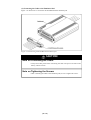
Preface
The M306V2T-RPD-E is an emulation pod for the M306V2 and M306V5 of 16-bit microcomputers.
It's used with a PC4701 emulator.
This user's manual mainly describes specifications of the M306V2T-RPD-E emulation pod and how
to setup it. For details on the following products, which are used with M306V2T-RPD-E, refer to each
product's user's manual.
• Emulator: PC4701M/PC4701HS/PC4701L User's Manual
• Emulator debugger: M3T-PD30 User's Manual
All the components of this product are shown in "2.2 Package Components" (page 19) of this user's
manual. If there is any question or doubt about this product, contact your local distributor.
To use the product properly
Precautions for Safety
• In both this User's Manual and on the product itself, several icons are used to insure
proper handling of this product and also to prevent injuries to you or other persons,
or damage to your properties.
• The icons' graphic images and meanings are given in "Chapter 1. Precautions for
Safety". Be sure to read this chapter before using the product.
When using outside Japan
• When using in Europe, the United States, or Canada, be sure to use both the emulator
and the emulation pod which meet overseas standards. EMI standards are not met
when the M306V2T-RPD-E is used with the PC4700H or PC4700L emulator.
( 3 / 72 )
Contents
Chapter 1. Precautions for Safety ........................................................................................... 7
1.1 Safety Symbols and Meanings .............................................................................. 8
Chapter 2. Preparation .......................................................................................................... 17
2.1 Terminology ........................................................................................................ 18
2.2 Package Components .......................................................................................... 19
2.3 Other Tool Products Required for Development ................................................ 19
2.4 Name of Each Part .............................................................................................. 20
(1) System Configuration ............................................................................... 20
(2) Inside of Emulation Pod ........................................................................... 21
2.5 When Using the Emulator for the First Time ...................................................... 22
Chapter 3. Setting Up ........................................................................................................... 23
3.1 Removing the Upper Cover ................................................................................ 24
3.2 Switch Settings .................................................................................................... 25
3.3 Selecting Clock Supply ....................................................................................... 29
(1) Using the Oscillator Circuit on the Target System .................................. 30
(2) Changing the Internal Oscillator Circuit of Emulation Pod ..................... 31
(3) Replacing the Oscillator Circuit Boards .................................................. 32
3.4 Circuits of Data Slicer I/O Signal and OSD Clock I/O Signal ........................... 33
3.5 A-D Conversion Bypass Capacitor ..................................................................... 35
3.6 Connecting the PC4701 and Emulation Pod ....................................................... 36
(1) Connecting the Cable to the PC4701 ....................................................... 36
(2) Connecting the Cable to the Emulation Pod ............................................ 37
3.7 Connecting the Target System ............................................................................ 38
Chapter 4. Usage .................................................................................................................. 39
4.1 Turning On the Power ......................................................................................... 40
(1) Checking the Connection of Emulator System ........................................ 40
(2) Turning On the Power .............................................................................. 40
(3) LED Display When PC4701 Starts Up Normally .................................... 41
4.2 Downloading Firmware ...................................................................................... 42
(1) When It is Necessary to Download Firmware ......................................... 42
(2) Downloading Firmware in Maintenance Mode ....................................... 42
4.3 Self-checks .......................................................................................................... 43
(1) Self-check Procedure ............................................................................... 43
(2) If an Error is Detected in Self-checks ...................................................... 43
( 4 / 72 )
Chapter 5. Specifications ...................................................................................................... 45
5.1 Specifications ...................................................................................................... 46
5.2 Operation Timing in Memory Expansion and Microprocessor Modes (5V) ...... 47
(1) Separate Bus, No-Wait ............................................................................. 47
(2) Separate Bus, With Wait, Accessing External Memory Area .................49
(3) Multiplex Bus, With Wait, Accessing External Memory Area ............... 51
(4) Timing Requirements ............................................................................... 53
5.3 Electrical Characteristics ..................................................................................... 55
5.4 Connection Diagram ........................................................................................... 56
5.5 External Dimensions ........................................................................................... 58
(1) External Dimensions of Emulation Pod ................................................... 58
(2) External Dimensions of Pitch Converter Board (FLX-100LCC) ............ 59
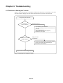
Chapter 6. Troubleshooting .................................................................................................. 61
6.1 Flowchart to Remedy the Troubles ..................................................................... 62
6.2 When the Emulator Debugger Does Not Start Up Properly ............................... 63
(1) When the LED Display of PC4701 is Abnormal ..................................... 63
(2) Errors Occur When the Emulator Debugger Starts Up
(When the target system is connected) .................................... 64
(3) Errors Occur When the Emulator Debugger Starts Up
(When the target system is not connected) .............................65
6.3 Operation Differs from That of Actual MCUs .................................................... 65
(1) A-D Conversion Values are Different from Expected Values ....................65
Chapter 7. Maintenance and Guarantee ................................................................................ 67
7.1 Maintenance ........................................................................................................ 68
7.2 Guarantee ............................................................................................................ 68
7.3 Repair Provisions ................................................................................................ 68
7.4 How to Request for Repair .................................................................................. 69
( 5 / 72 )
MEMO
( 6 / 72 )
Chapter 1. Precautions for Safety
This chapter describes precautions for using this product safely and properly. For precautions for the emulator main unit
and the emulator debugger, refer to each user's manual included with your product.
1.1 Safety Symbols and Meanings ..................................................................................................... 8
WARNING
Warning for Installation ............................................................................................... 9
Warnings for Use Environment ................................................................................... 9
CAUTION
Caution to Be Taken for Modifying This Product ....................................................... 9
Cautions to Be Taken for This Product........................................................................ 9
IMPORTANT
Note on Malfunctions in the PC4701 System .............................................................. 9
Notes on Downloading Firmware .............................................................................. 10
Notes on Target System ............................................................................................. 10
Note on Reset Input ................................................................................................... 10
Notes on Watchdog Function..................................................................................... 10
Note on When the Emulator Debugger Ends ............................................................. 10
Note on DMA Transfer .............................................................................................. 11
Note on Setting the Work Area .................................................................................. 11
Notes on Stack Area................................................................................................... 11
Note on Address 0 Access ......................................................................................... 11
Note on Stop and Wait Modes ................................................................................... 11
Notes on MAP References and Settings .................................................................... 12
Notes on S/W Breaks and H/W Breaks ..................................................................... 12
Note on BRK Instruction ........................................................................................... 12
Note on NMI* Input................................................................................................... 13
Notes on HOLD* Input .............................................................................................. 13
Notes on Address Match Interrupt ............................................................................. 13
Note on Software Reset ............................................................................................. 13
Note on Protect Resister (PRC2) ............................................................................... 13
Note on Setting BCLK Output Disable Bit (PM07) .................................................. 13
Note on Differences between Actual MCU and Emulator ........................................ 14
( 7 / 72 )
Chapter 1. Precautions for Safety
In both the user's manual and on the product itself, several icons are used to insure proper handling
of this product and also to prevent injuries to you or other persons, or damage to your properties.
This chapter describes the precautions which should be taken in order to use this product safely and
properly. Be sure to read this chapter before using this product.
1.1 Safety Symbols and Meanings
WARNING
If the requirements shown in the "WARNING"
sentences are ignored, the equipment may
cause serious personal injury or death.
CAUTION
If the requirements shown in the "CAUTION"
sentences are ignored, the equipment may
malfunction.
IMPORTANT
It means important information on using this
product.
In addition to the three above, the following are also used as appropriate.
means WARNING or CAUTION.
Example:
CAUTION AGAINST AN ELECTRIC SHOCK
means PROHIBITION.
Example:
DISASSEMBLY PROHIBITED
means A FORCIBLE ACTION.
Example:
UNPLUG THE POWER CABLE FROM THE RECEPTACLE.
The following pages describe the symbols "WARNING", "CAUTION", and "IMPORTANT".
( 8 / 72 )
WARNING
Warning for Installation:
• Do not set this product in water or areas of high humidity. Spilling water or some other liquid into
the main unit can cause an unrepairable damage.
Warnings for Use Environment:
• The emulation pod is air-cooled with the ventilation slot. Therefore, do not block the ventilation
slot. When heated to high temperatures, the emulation pod may not work properly.
• This equipment is to be used in an environment with a maximum ambient temperature of 35°C. Care
should be taken that this temperature is not exceeded.
CAUTION
Caution to Be Taken for Modifying This Product:
• Do not disassemble or modify this product. Disassembling or modifying this product can cause
damage. Disassembling and modifying the product will void your warranty.
Cautions to Be Taken for This Product:
• Use caution when handling the main unit. Be careful not to apply a mechanical shock.
• Do not touch the connector pins of the emulator main unit and the target MCU connector pins . Static
electricity may damage the internal circuits.
• Do not pull the emulation pod main unit by the flexible cable (FLX120-RPD) for connecting to the
emulator main unit or the flexible cable (FLX64, FLX100 or FLX160) for connecting the target
system. The cable may cause a break.
• The flexible cable (FLX120-RPD) for connecting to the emulator main unit and the flexible cable
(FLX64, FLX100 or FLX160) for connecting the target system are different from earlier models.
The slits make them more flexible. However, excessive flexing or force may break conductors.
• Do not use inch-size screws for this equipment. The screws used in this equipment are all ISO
(meter-size) type screws. When replacing screws, use same type screws as equipped before.
IMPORTANT
Note on Malfunctions in the PC4701 System
• If the emulator malfunctions because of interference like external noise, do the following to remedy
the trouble.
(1) Press the RESET switch on the emulator front panel.
(2) If normal operation is not restored after step (1), shut OFF power to the emulator once and then
reactivate it.
( 9 / 72 )
IMPORTANT
Notes on Downloading Firmware:
• Before using this product for the first time, it is necessary to download the dedicated firmware
(control software for the emulation pod built into the PC4701). Please note that, to do this, it is
necessary to start up the PC4701 in the maintenance mode. For firmware download procedures, see
"4.2 Downloading Firmware" (page 42). Once the firmware has been downloaded, the product can
be used by simply turning on the power.
• Do not shut off the power while downloading the firmware. If this happens, the product will not
start up properly. If power is shut off unexpectedly, redownload the firmware.
• Except when a target status error occurs, if self-checks are not completed successfully, there may
be trouble with the product. In such case, contact your sales representative. However, perform selfchecks in the below setup.
(1) Target system:
Not connected
(2) Emulation pod internal switches: At their factory settings
Notes on Target System:
• The Vcc pin of emulator is connected to the target system to observe the voltage of the target system.
For this reason, it is impossible to supply the power from the emulator to the target system.
Therefore design your system so that the target system is powered separately.
• The voltage of the target system should be within the range of the MCU specification.
• Do not change the voltage of the target system after turning on the power.
• Before powering on your emulator system, check that the host machine, the emulator main unit,
the converter board and target system are all connected correctly. Next, turn on the power to each
equipment following the procedure below.
(1) Turn ON/OFF the target system and the PC4701 emulator as simultaneously as possible.
(2) When the PC4701 and emulator debugger start up, check the target status LEDs on the
emulator main unit's front panel to see if this product is ready to operate.
• Is the power supplied?
Check that target status LED (POWER) is ON.
For details, refer to "Chapter 4. Usage" (page 39).
Note on Reset Input:
• The reset input from the target system is accepted only while a user program is being executed (only
while the RUN status LED on the PC4701's front panel is lit).
Notes on Watchdog Function:
• The MCU's watchdog timer can be used only while programs are being executed. To use it
otherwise, disable the timer.
• If the reset circuit of the target system has a watchdog timer, disable it when using the emulator.
Note on When the Emulator Debugger Ends:
• To restart the emulator debugger after it ends, always shut power to the emulator module off once
and then on again.
( 10 / 72 )
IMPORTANT
Note on DMA Transfer:
• With this product, the program is stopped with a loop program to a specific address. Therefore, if
a DMA request is generated by a timer or other source while the program is stopped, DMA transfer
is executed. However, make note of the fact that DMA transfer while the program is stopped may
not be performed correctly. Also note that the below registers have been changed to generate DMA
transfer as explained here even when the program is stopped.
DMA0 transfer counter register TCR0
DMA1 transfer counter register TCR1
Note on Setting the Work Area:
• To use this product, it is necessary to set the work area in the internal reserved area of the MCU.
However, do not set it in the last 10 bytes of the internal reserved area. And be sure to set the internal
reserved area to INTERNAL. (Set the work area by the INIT dialog of emulator debugger M3TPD30.)
Example: When debugging the program of the MCU whose internal reserved area is 0180016 to
02BFF16, set the work area within the range of 0180016 to 02BF616.
For instance, when setting the work area at 0180016, the emulator uses 10 bytes area of 0180016 to
0180916.
Notes on Stack Area:
• With this product, a maximum 8 bytes of the user stack is consumed.
• If the user stack does not have enough area, do not use areas which cannot be used as stack (SFR
area, RAM area which stores data, or ROM area) as work area. Using areas like this is a cause of
user program crashes and destabilized emulator control. Therefore, ensure the +8 bytes maximum
capacity used by the user program as the user stack area.
Note on Address 0 Access:
• With the M306V2 and M306V5 MCUs, when a maskable interrupt is generated, the interrupt data
(interrupt No. and interrupt request level) stored in address 0 is read out. Also, the interrupt request
bit is cleared when address 0 is read out. Consequently, when the address 0 readout instruction is
executed or when address 0 is read out in the cause of a program runaway, a malfunction occurs
in that the interrupt is not executed despite the interrupt request, because the request bit of the
highest priority interrupt factor enabled is cleared.
For this malfunction, when the reading out to the 0 address is generated excluding the interrupt, the
yellow LED lights up to alarm. When this LED lights, there is a possibility of wrong access,
therefore check the program. This LED is turned off by the RESET switch of the emulator main
unit.
Note on Stop and Wait Modes:
• Do not perform step execution at addresses in the stop or wait mode. It may cause communication
errors.
( 11 / 72 )
IMPORTANT
Notes on MAP References and Settings:
• For details on referencing and setting MAP information, see User's Manual of emulator debugger
M3T-PD30.
• Be sure to set the SFR area to EXTERNAL.
• When setting 0FFFC16 to 0FFFF16 to EXTERNAL:
This product uses the 4 byte area 0FFFC16 to 0FFFF16 as the stack area when the RESET command
of emulator debugger M3T-PD30 is executed. If this 4 byte memory cannot be read or written to,
reset cannot be properly effected. As a result, you need to alter the map settings if the condition
given below is met.
(1) With the system which shifts from the single-chip mode to the memory expansion (or
microprocessor) mode, using the 4-byte area of 0FFFC16 to 0FFFF16 set to EXTERNAL.
(2) With the system which starts up in microprocessor mode, using the 4-byte area of 0FFFC16
to 0FFFF16 set to EXTERNAL and there is not enough memory to read or write.
The procedures to alter the MAP settings when the conditions (1) or (2) above are met.
(1) Set the 4-byte area of 0FFFC16 to 0FFFF16 to INTERNAL.
(2) Execute the RESET command by use of emulator debugger M3T-PD30.
(3) Set the stack pointer.
(Example)
RESET:
I
#4000H, SP <-- Set the stack pointer
(Stop the program after executing this instruction)
○
○
FCLR
LDC
(4) Set the 4-byte area 0FFFC16 through 0FFFF16 to EXTERNAL.
Notes on S/W Breaks and H/W Breaks:
• S/W breaks generate BRK interrupts by substituting the proper instruction to the BRK instruction.
Therefore, when referencing the result of a trace in bus mode, "0016" is displayed for the instruction
fetch address where a software break is set, and when referencing in reverse assemble mode,
"BRK" instruction is displayed.
• It is not possible to use a S/W break and a H/W break at the same time. If doing so, it may not operate
normally.
• In the area where the MAP setting is EXTERNAL, S/W breaks cannot be used.
Note on BRK Instruction:
• BRK instruction cannot be used.
( 12 / 72 )
IMPORTANT
Note on NMI* Input:
• NMI* input from the target system is accepted only while a user program is being executed (only
while the RUN status LED on the PC4701's front panel is lit).
Notes on HOLD* Input:
• Be sure to input "Low" to the HOLD* pin of the target system during the user program executing
(while the RUN status LED on the PC4701's front panel is lit). Inputting "Low" to the HOLD* pin
when stopping the user program or when run-time debugging may cause a malfunction of the
emulator.
• When inputting "Low" to the HOLD* pin to run into the HOLD state, P00 to P52 will be in the HOLD
state delaying by 2.5 cycles than the actual MCU (see Table 5.5, Figure 5.5).
Notes on Address Match Interrupt:
• Do not set software breaks at the same addresses as address-match interrupts as the program may
run out of control.
• Do not set a hardware break within 4 instructions before an address at which an address-match
interrupt occurs. If you do set a hardware break in this range, the program will run out of control.
• When an address at which an address-match interrupt occurs is executed in one-step mode, the
program stops after executing the first instruction after returning from the address-match interrupt
processing.
Note on Software Reset:
• Do not use a software reset.
Note on Protect Resister (PRC2):
• Make note of the fact that the protect is not canceled when the protect register (PRC2), which
enables writing in the port P9 direction register, is changed with the below procedure.
(1) Step execution of the "instruction for setting ("1") PRC2".
(2) Setting the break point from the "instruction for setting ("1") PRC2" to the "setting the register
for the protect".
(3) "Setting ("1") PRC2" from the dump window, script window or others.
Note on Setting BCLK Output Disable Bit (PM07):
• Do not set the 7th bit (PM07: BCLK output disable bit) of the processor mode register 0 (address
000416) to "1". Otherwise, this emulation pod does not work properly.
( 13 / 72 )
IMPORTANT
Note on Differences between Actual MCU and Emulator:
• Operations of the emulator differs from those of actual MCUs as listed below.
(1) Reset condition
Set the time for starting up (0.2Vcc to 0.8Vcc) 1µs or less.
(2) Data values of ROM area at power-on
(3) Internal memories (RAM and ROM) capacities etc.
(4) Characteristics of Port P00 to P57
Ports P00 to P57 are connected via port emulation circuits. The device used for the port
emulation circuit is:
Device: M60074-0111FP
(5) A-D input
As a flexible cable, a pitch converter board and other devices are used between the evaluation
MCU and the target system, some characteristics are slightly different from those of the actual
MCU. Therefore, be sure to evaluate your system with an evaluation MCU. Before starting
mask production, evaluate your system and make final confirmation with an ES (Engineering
Sample) version MCU.
(6) Pull-up control
Port P0-P5 pullup control in this product is different between modes as shown in Table 1.1.
There is not difference for ports P6 to P10.
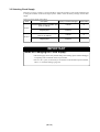
Table 1.1 P0-P5 Pullup control
Single-chip mode
Memory expansion/microprocessor mode
Actual MCU
(1) Enabled for only input Disabled
ports
(Enabled if P44 (CS0) to P47 (CS3) are used
(2) Can be set bitwise as input ports, however.)
This
emulation
pod
(1) Always enabled irrespective of operation mode
(Also enabled when used as address/data bus or output ports)
(2) Cannot be set bitwise
Can only be set in units of 4 bits (P00-P03, P04-P07, ... P50-P53,
P54-P57). If any bit in the 4-bit unit is enabled for pullup, all of the four
bits are enabled for pullup.
(7) Write to pullup control registers 0, 1 (addresses 03FC16, 03FD16)
When you write to pullup control registers 0, 1 (addresses 03FC16, 03FD16), always be sure
to write in units of words beginning with address 03FC16.
This paragraph constitutes a limitation on M306V2T-RPD-E.
(8) Ports P50-P53
When you enable the pullup resistors of these ports in single-chip mode by setting pullup
control register 1 bit 2 (PUR12) to "1", always be sure to set processor mode register 0 bit 2
(PM02) and bit 7 (PM07) both to "0".
This paragraph constitutes a limitation on M306V2T-RPD-E.
( 14 / 72 )
IMPORTANT
(9) Outputs of the actual MCU and this product
Table 1.2 Differences of outputs between actual MCU and this product (when executing program)
Access area
SFR area
(MAP=EXT)
Internal RAM
Signal
Actual MCU
This product
Address
BHE*
Outputs
Outputs
Data
Outputs
(floating during read operating)
Floating
∗
RD*
WR*
Outputs
(WR*=Low at write cycle,
RD*=Low at read cycle)
Does not output
∗
CS*
Does not output
(fixed to High output)
Does not output
(fixed to High output)
ALE
Does not output
(fixed to Low output)
Outputs
∗
Address
BHE*
Retains previous status
Outputs
∗
Data
Floating
Floating
RD*
WR*
Does not output
(fixed to High output)
Does not output
(fixed to High output)
CS*
Does not output
(fixed to High output)
Does not output
(fixed to High output)
ALE
Does not output
(fixed to Low output)
Outputs
Address
BHE*
Outputs
Outputs
Data
Outputs
(inputs external data at read cycle)
Outputs
(inputs external data at read cycle)
RD*
WR*
Outputs
(WR*=Low at write cycle,
RD*=Low at read cycle)
Outputs
(WR*=Low at write cycle,
RD*=Low at read cycle)
CS*
Outputs
Outputs
ALE
Outputs
Outputs
Internal ROM
External area
∗ for difference
∗
Table 1.3 Differences of outputs between actual MCU and this product (when stopping program)
Access area
Signal
Actual MCU
This product
Address
BHE*
Outputs
Data
Floating
RD*
WR*
Outputs RD* only
(WR* is fixed to High output)
CS*
Outputs
ALE
Outputs
( 15 / 72 )
∗ for difference
IMPORTANT
Table 1.4 Differences of outputs between actual MCU and this product (in stop mode)
Access area
Signal
Actual MCU
This product
Address
BHE*
Retains previous status
Retains previous status
Data
Retains previous status
Floating
RD*
WR*
Does not output
(fixed to High output)
Does not output
(fixed to High output)
CS*
Retains previous status
Retains previous status
ALE
Does not output
(fixed to High output)
Does not output
(fixed to High output)
∗ for difference
∗
Table 1.5 Differences of outputs between actual MCU and this product (in wait mode)
Access area
Signal
Actual MCU
This product
Address
BHE*
Retains previous status
Retains previous status
Data
Retains previous status
Floating
RD*
WR*
Does not output
(fixed to High output)
Does not output
(fixed to High output)
CS*
Retains previous status
Retains previous status
ALE
Does not output
(fixed to High output)
Does not output
(fixed to High output)
( 16 / 72 )
∗ for difference
∗
Chapter 2. Preparation
This chapter describes the package components, the system configuration and the preparation for using this product for the
first time.
2.1 Terminology ............................................................................................................................... 18
2.2 Package Components.................................................................................................................. 19
2.3 Other Tool Products Required for Development........................................................................ 19
2.4 Name of Each Part ...................................................................................................................... 20
(1) System Configuration ........................................................................................................... 20
(2) Inside of Emulation Pod ....................................................................................................... 21
2.5 When Using the Emulator for the First Time ............................................................................. 22
( 17 / 72 )
Chapter 2. Preparation
2.1 Terminology
Some specific words used in this user's manual are defined as follows:
Emulator system
This means an emulator system built around the PC4701 emulator. The PC4701 emulator system is
configured with an emulator main unit, emulation pod, host machine and emulator debugger.
Emulator main unit (Hereafter PC4701)
This means a generic name for emulators for 8 and 16-bit MCUs. For details on specific models of
PC4701, visit the Renesas Tools Homepage.
http://www.renesas.com/en/tools
Emulation pod
This means M306V2T-RPD-E (this product). This emulation pod is for M306V2 and M306V5
MCUs.
Host machine
This means a personal computer used to control the emulator and emulation pod.
Emulator debugger
This means a software tool M3T-PD30 to control the emulator from the host machine through an
interface.
Firmware
Program that analyzes contents of communication with the emulator debugger and controls the
emulator hardware. This program is installed in the EEPROM. This program is downloadable from
the emulator debugger to upgrade the firmware or to support other MCUs.
Evaluation MCU
This means the microcomputer mounted on the emulation pod which is operated in the specific mode
for tools.
Target MCU
This means the microcomputer you are going to debug.
Target system
This means a user's application system using the microcomputer to be debugged.
*
In this user's manual, this symbol is used to show active "Low". (e.g. RESET*: Reset signal)
( 18 / 72 )
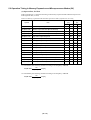
2.2 Package Components
The M306V2T-RPD-E package consists of the following items. When unpacking, check to see if
your M306V2T-RPD-E contains all of these items.
Quantity
Item
M306V2T-RPD-E emulation pod main unit
1
FLX120-RPD flexible cable for connecting PC4701
1
FLX100 flexible cable for connecting pitch converter board (pre-installed in emulation pod)
1
FLX-100LCC pitch converter board for connecting target system
1
OSC-3 (10MHz) oscillator circuit board (pre-installed in emulation pod)
1
OSC-2 (32.768kHz) oscillator circuit board (pre-installed in emulation pod)
1
OSC-2 oscillator circuit board
1
Hardware tool user registration FAX sheet (English)
1
Hardware tool user registration FAX sheet (Japanese)
1
M306V2T-RPD-E user's manual (this manual)
1
M306V2T-RPD-E user's manual (Japanese)
1
Please keep the M306V2T-RPD-E’s packing box and cushion material in your place for reuse at a
later time when sending your product for repair or other purposes. Always use these packing box and
cushion material when transporting this product.
If any of these items are missing or found faulty, please contact your local distributor. Also, if there
is any question or doubt about the packaged product, contact your local distributor.
2.3 Other Tool Products Required for Development
To bring forward programs development on the M306V2 and M306V5 MCUs, the products listed
below are necessary in addition to those contained package above. Get them separately.
Emulator main unit
PC4701
Emulator debugger
M3T-PD30
Pitch converter board
(Required for M306V5 MCU)
M306V5T-PTC
100D0
PCA7412L-100 (necessary for OSD ROM)
M306V2
100P6S
Programming adapter
PCA7412F-100 (necessary for OTP version)
PCA7412L-100 (necessary for OSD ROM)
M306V5
PCA7412E4S-64 (necessary for EPROM version or
OTP version)
To purchase these products, contact your nearest distributer.
( 19 / 72 )
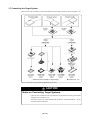
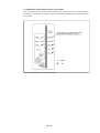
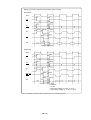
2.4 Name of Each Part
(1) System Configuration
Figure 2.1 System configuration
(1) to (4) in Figure 2.1 are included with this product package.
(1) Emulation pod (M306V2T-RPD-E)
This emulation pod contains an evaluation MCU, emulation memory and circuit to feature the
debugging functions.
(2) Flexible cable (FLX120-RPD)
This is a 120-pin flexible cable for connecting the PC4701 emulator and the emulation pod.
(3) Flexible cable (FLX100)
This is a 100-pin flexible cable for connecting the emulation pod and the target system.
(4) Pitch converter board
This is a pitch converter board for connecting to the target system. For details, refer to "3.7
Connecting the Target System" (page 38).
( 20 / 72 )
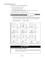
(2) Inside of Emulation Pod
Figure 2.2 Internal view of emulation pod
(1) MCU-dependent board
Board which groups parts (pins and added functions) which vary according to MCU model.
(2) Base board
Board for the M16C/60 Series MCUs which controls the interface with the PC4701 and the
evaluation MCU.
(3) Memory board
Board on which is mounted the emulation memory (1MB) and the map memory (4 bits×1M) for
the M16C/60 Series MCUs.
(4) Oscillation circuit board
Oscillator circuit board on which the 10.000MHz of oscillation module device and 32.768kHz
of crystal oscillator are mounted.
( 21 / 72 )
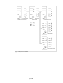
2.5 When Using the Emulator for the First Time
If you have purchased this emulation pod newly, it is necessary to download the firmware. The
download procedure is given in Figure 2.3.
Before attempting to download the firmware, check the emulator debugger is installed and the
emulator is connected to the host machine. For more information, see each user's manual of the
emulator debugger and the PC4701.
Connect the PC4701 and this product.
See "3.6 Connecting the PC4701
and Emulation Pod" (page 36).
Within 2 seconds of turning the power ON, press the
RESET switch of the PC4701 and check the maintenance
mode is accessed.
See "4.2 Downloading Firmware"
(page 42).
Download the firmware using the emulator debugger.
End the emulator debugger and shut the power of the
PC4701 OFF.
Figure 2.3 Firmware download procedure when emulator is used for the first time
To make sure the emulation pod works properly, run the self-checks. For self-check procedures, see
"4.3 Self-checks" (page 43).
( 22 / 72 )
Chapter 3. Setting Up
This chapter describes switch settings required for using this product and how to connect this product to the PC4701 and
the target system.
3.1 Removing the Upper Cover ........................................................................................................ 24
3.2 Switch Settings ........................................................................................................................... 25
3.3 Selecting Clock Supply .............................................................................................................. 29
(1) Using the Oscillator Circuit on the Target System ............................................................... 30
(2) Changing the Internal Oscillator Circuit of Emulation Pod ................................................. 31
(3) Replacing the Oscillator Circuit Boards ............................................................................... 32
3.4 Circuits of Data Slicer I/O Signal and OSD Clock I/O Signal .................................................... 33
3.5 A-D Conversion Bypass Capacitor.............................................................................................. 35
3.6 Connecting the PC4701 and Emulation Pod .............................................................................. 36
(1) Connecting the Cable to the PC4701 .................................................................................... 36
(2) Connecting the Cable to the Emulation Pod ......................................................................... 37
3.7 Connecting the Target System.................................................................................................... 38
( 23 / 72 )
Chapter 3. Setting Up
To use this emulation pod with your target system, it is necessary to set as follows. Set the following
after removing the upper cover.
• Set the switches in the emulation pod corresponding to the condition of the target system.
• Change the oscillation frequency of the emulation pod.
• Change the input frequency of the OSD oscillation.
• Change the constant number of the data slicer I/O signal circuit.
• Install the A-D conversion bypass capacitor.
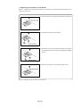
3.1 Removing the Upper Cover
The procedure of removing the upper cover is shown below.
(1) Remove the four screws of both sides of this product and lift off the upper cover. (see Figure 3.1)
(2) Set the switches following the descriptions below.
(3) Replace the upper cover and secure the four screws.
Figure 3.1 Removing the upper cover
CAUTION
Notes on Removing the Upper Cover:
• Always shut OFF power when removing the upper cover or setting the switches.
• Do not touch the connector pins of the emulator main unit and the target MCU
connector pins. Static electricity may damage the internal circuits.
( 24 / 72 )
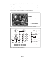
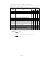
3.2 Switch Settings
Figure 3.2 shows the positions of switches of the M306V2T-RPD-E. Table 3.1 lists how to set
switches.
Figure 3.2 Positions of switches and their factory-settings
( 25 / 72 )
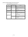
Table 3.1 Switch settings of M306V2T-RPD-E (part 1)
Signal
Switch
Setting
Description
OSD
SW1
P57
Be sure to use this switch in the factory-setting.
PORT
P57/OSD
SW1
(Factory-setting)
SW1
P57
OSD
Can not be used.
PORT
XCIN
Connects P87/XCIN pin of MCU to the target system.
(Uses P87/XCIN pin as port P87.)
P87/XCIN
SW2
P87
SW2
(Factory-setting)
XCIN
Uses P87/XCIN pin as XCIN.
P87
SW2
XCOUT
Connects P8 6/X COUT pin of MCU to the target
system. (Uses P86/XCOUT pin as port P86.)
P86
SW3
(Factory-setting)
XCOUT
P86/XCOUT
Does not connect P86/XCOUT pin of MCU to the
target system. (Uses P86/XCOUT pin as XCOUT and
opens XCOUT.)
SW3
P86
SW3
XCOUT
Connects P8 6/X COUT pin of MCU to the target
system. (Uses P86/XCOUT pin as XCOUT and connects
XCOUT to the target system.)
P86
SW3
( 26 / 72 )
Table 3.1 Switch settings of M306V2T-RPD-E (part 2)
Signal
Switch
Setting
Description
XOUT
Does not connect XOUT pin of MCU to the target
system.
XOUT
SW4
OPEN
SW4
(Factory-setting)
XOUT
Connects XOUT pin of MCU to the target system.
OPEN
SW4
OPEN
SW5
HOLD
RDY
HOLD/RDY
Pulls up HOLD/RDY pin of MCU at 33kΩ.
H
SW5
(Factory-setting)
OPEN
HOLD
RDY
Opens HOLD/RDY pin of MCU.
H
SW5
CNVSS
H
Pulls down CNVSS pin of MCU at 33kΩ.
L
SW6
(Factory-setting)
CNVSS
H
CNVSS
SW6
Does not pull down/up CNVSS pin of MCU.
L
SW6
CNVSS
H
Pulls up CNVSS pin of MCU at 33kΩ.
L
SW6
( 27 / 72 )
Table 3.1 Switch settings of M306V2T-RPD-E (part 3)
Signal
Switch
Setting
Description
BYTE
8
Pulls down BYTE pin of MCU at 33kΩ.
16
SW7
(Factory-setting)
BYTE
8
BYTE
SW7
Does not pull down/up BYTE pin of MCU.
16
SW7
BYTE
8
Pulls up BYTE pin of MCU at 33kΩ.
16
SW7
P70/71
OPEN
Does not pull up P70 and P71.
P70/P71
SW8
H
SW8
(Factory-setting)
P70/71
OPEN
Pulls up P70 and P71 at 470Ω.
H
SW8
( 28 / 72 )
3.3 Selecting Clock Supply
There are two ways to supply a clock to the MCU, using the oscillator circuit of the emulation pod
or using the oscillator circuit on the target system. Table 3.2 lists the factory-settings of each clock
supply.
Table 3.2 Clock supply to the MCU
Clock
Description
Display of emulator debugger Default setting
Internal oscillator circuit of emulation pod
(OSC-3: 10MHz)
Internal
O
Target System
External
-
Internal oscillator circuit of emulation pod
(OSC-2: 32.768kHz)
Internal
O
Target System
External
-
XIN-XOUT
XCIN-XCOUT
IMPORTANT
Notes on Changing the Clock Supply:
• The clock supply can be set by the Init dialog when starting up the emulator debugger
or inputting CLK command on the script window.
• For XCIN-XCOUT pins, it is necessary to set switches in the emulation pod. For details,
refer to "3.2 Switch Settings" (page 25).
( 29 / 72 )
(1) Using the Oscillator Circuit on the Target System
When turning on the power, the internal clock of emulation pod is selected to supply the clock to the
MCU. To use the external clock on the target system, change the clock by the Init dialog when starting
up the emulator debugger or the CLK command on the script window. (For details, refer to the user's
manual of the emulator debugger.)
Figure 3.3 External oscillator circuit
Figure 3.4 Circuit in which oscillation does not occur (same for XCIN-XCOUT)
IMPORTANT
Notes on Using the Oscillator Circuit on the Target System:
• To operate the emulation pod with an external clock, construct the oscillator circuit
as shown in Figure 3.3 in the target system and input the oscillator output at 50% duty
(within the operating range of the evaluation MCU) into the XIN pin. And the XOUT
pin should be open.
• Make note of the fact that in the oscillator circuit shown in Figure 3.4 where a
resonator is connected between the XIN and XOUT pins, oscillation does not occur
because a flexible cable, pitch converter board and other devices are used between
the evaluation MCU and the target system. It is same for sub-clock oscillator circuits
(XCIN and XCOUT).
( 30 / 72 )
(2) Changing the Internal Oscillator Circuit of Emulation Pod
An oscillator circuit board for 10MHz is mounted on this product. To use the emulation pod at a
frequency other than 10MHz, build the desired oscillator circuit on the included OSC-2 oscillator
circuit board (bare board) and replace the board installed in the emulation pod when shipped from
the factory.
Figure 3.5 shows a view of the OSC-2 oscillator circuit board (bare board) and where connector pins
are located. Figure 3.6 shows the circuitry of the OSC-2 oscillator circuit board (bare board). Use the
number of oscillator circuits recommended by the oscillator manufacturer.
J1-4: GND
J1-3: Oscillator output
J1-2: GND
J1-1: Vcc
Bypass capacitor
Figure 3.5 External view of oscillator board (OSC-2) and connector pin assignment
IC1
11
IC1
10
CLK
8
9
J1-3
R1
*
*
X1 ,X 2
C2
*
X3
Vcc
2
1
R2
C1
3
4
5
6
7
13
12
GND
IC1
* X1: 5.08-mm-pitch 2-pin oscillator
* X2: 2.54-mm-pitch 2-pin oscillator
* X3: 2.54-mm-pitch 3-pin oscillator
Figure 3.6 Circuit of oscillator board (OSC-2)
( 31 / 72 )
C3
J1-1
14
IC1
J1-2
J1-4
GND
IC1: Inverter (Unbuffer)
(3) Replacing the Oscillator Circuit Boards
Figure 3.7 shows how to replace the oscillator circuit boards. For the position of the oscillator circuit
board, see Figure 2.2.
(1) Unscrew the screw connecting the oscillator circuit board.
(2) Lift off the oscillator circuit board.
(3) Attach the J1 connector of another oscillator circuit board
for replacement to the J5 connector of the MCU-dependent
board.
(4) Secure the oscillator circuit board with the screw.
Figure 3.7 Replacing the oscillator circuit boards
( 32 / 72 )
3.4 Circuits of Data Slicer I/O Signal and OSD Clock I/O Signal
With this product, the parts used for the data slicer and OSD clock circuit are attached by sockets for
replacement. Figure 3.8 shows the position of each part used for the data slicer and OSD clock
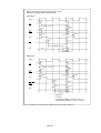
circuits, and Figures 3.9 to 3.12 show the circuit diagram and the constants of board-mounted parts.
Figure 3.8 Position of each part
(1) Figure 3.9 shows the numbers of parts which are connected to the CVIN pin, the constants of parts
and the connection circuits.
Figure 3.9 Signal circuits of CVIN pin
( 33 / 72 )
(2) Figure 3.10 shows the numbers of parts which are connected to HLF pin, the constants of parts
and the connection circuits.
Figure 3.10 Signal circuits of HLF pin
(3) Figure 3.11 shows the number of part which is connected to VHOLD pin, the constant of part and
the connection circuit.
Figure 3.11 Signal circuit of VHOLD pin
(4) Figure 3.12 shows the numbers of parts which are connected to OSC1 and OSC2 pins, the
constants of parts and the connection circuits.
Figure 3.12 Signal circuits of OSC1 and OSC2 pins
( 34 / 72 )
3.5 A-D Conversion Bypass Capacitor
Figure 3.13 shows the foot pattern of the A-D conversion bypass capacitor. The emulation pod has
foot patterns between AVCC and AVSS (C54) on the reverse side of the M306V0T-PRT for mounting
a bypass capacitor. Mount a suitable bypass capacitor as occasion demands.
AVCC-AVSS bypass capacitor
Figure 3.13 Foot patterns of A-D conversion bypass capacitor
IMPORTANT
Note on the A-D Converter:
• Because a flexible board and other devices are used between the emulator MCU and
the target system, the A-D converter operates differently from the actual MCU.
Make the final evaluation of the A-D converter using the actual MCU.
( 35 / 72 )
3.6 Connecting the PC4701 and Emulation Pod
To connect the emulation pod to the PC4701, use the FLX120-RPD 120-pin flexible cable included
in this product package. Connect the PC4701 side connector of FLX120-RPD to the cable connector
of the PC4701, then secure the FLX120-RPD with the screws.
(1) Connecting the Cable to the PC4701
Figure 3.14 shows how to connect the PC4701 and FLX120-RPD.
Figure 3.14 Connecting PC4701 and FLX120-RPD
CAUTION
Note on Connecting the Cable:
• Always shut OFF power before connecting the cable. The power ON state could
destroy internal circuits.
Note on Tightening the Screws:
• After connecting the cable to the emulator main unit PC4701, be sure to tighten the
screws mounted in both sides of the connector.
( 36 / 72 )
(2) Connecting the Cable to the Emulation Pod
Figure 3.15 shows how to connect the FLX120-RPD and the emulation pod.
Figure 3.15 Connecting FLX120-RPD and emulation pod
CAUTION
Note on Connecting the Cable:
• Always shut OFF power before connecting the cable. The power ON state could
destroy internal circuits.
Note on Tightening the Screws:
• After connecting the cable to the emulation pod, be sure to tighten the screws.
( 37 / 72 )
3.7 Connecting the Target System
There are five ways available to connect the emulation pod to target systems as shown in Figure 3.16.
Figure 3.16 Connecting emulation pod and target systems
CAUTION
Notes on Connecting Target Systems:
• Take care not to attach the converter board in a wrong direction. It may cause a fatal
damage to the emulation pod.
• The small connectors of FLX100 and FLX-100LCC are guaranteed for only 20
insertion/removal iterations.
( 38 / 72 )
Chapter 4. Usage
This chapter describes from turning on the power of this product to starting up the emulator debugger.
4.1 Turning On the Power ................................................................................................................ 40
(1) Checking the Connection of Emulator System ..................................................................... 40
(2) Turning On the Power........................................................................................................... 40
(3) LED Display When PC4701 Starts Up Normally ................................................................ 41
4.2 Downloading Firmware .............................................................................................................. 42
(1) When It is Necessary to Download Firmware ...................................................................... 42
(2) Downloading Firmware in Maintenance Mode .................................................................... 42
4.3 Self-checks ................................................................................................................................. 43
(1) Self-check Procedure ............................................................................................................ 43
(2) If an Error is Detected in Self-checks ................................................................................... 43
( 39 / 72 )
Chapter 4. Usage
4.1 Turning On the Power
(1) Checking the Connection of Emulator System
Before turning the power ON, check the connection of the PC4701, emulation pod, converter board
and target system.
(2) Turning On the Power
Power ON/OFF the target system and the PC4701 as simultaneously as possible.
CAUTION
Notes on Power Supply:
• The emulator's VCC pin is connected to the target system in order to monitor target
system voltage. For this reason, the emulator cannot supply power to the target
system. Therefore, provide the target system with a separate power supply from that
of the emulator.
• Keep target system power supply voltage within the MCU's specified range.
• Do not change target system power supply voltage after power has been activated.
( 40 / 72 )
(3) LED Display When PC4701 Starts Up Normally
After the emulator starts up, check the status of the LEDs on the front panel to see whether emulation
pod operation is enabled or not. Figure 4.1 shows front panel LED lighting status when the emulator
is turned ON.
Figure 4.1 LED display when PC4701 turned on
( 41 / 72 )
4.2 Downloading Firmware
(1) When It is Necessary to Download Firmware
It is necessary to download firmware when;
(1) you use this product for the first time.
(2) the firmware has been upgraded.
(3) the emulator debugger has been upgraded.
(4) you use this product with a PC4701 which was used with other emulation pod before.
(2) Downloading Firmware in Maintenance Mode
Download the firmware in the maintenance mode as explained here following. The target system
must not be connected when downloading the firmware.
(1) Within 2 seconds of activating power to the emulator, press the RESET switch on the emulator
front panel. This will switch the emulator to the maintenance mode.
(2) Start up the emulator debugger. When the Init dialog box setup is complete, the dialog which
urges to download the firmware will appear. Download the firmware following messages.
Required time for downloading the firmware depends on the connection of the interface.
• For the serial interface ................ approx. 7 minutes
• For the parallel interface ............. approx. 30 seconds
Figure 4.2 Downloading firmware in maintenance mode
CAUTION
Note on Downloading Firmware:
• Do not shut OFF power while the firmware is being downloaded. Doing so, the
emulator will not start up properly. If power is shut OFF by mistake, redownload the
firmware in the maintenance mode.
( 42 / 72 )
4.3 Self-checks
(1) Self-check Procedure
To run the emulator self-checks, do so as explained here below. While self-checks are in progress,
LEDs will change as shown in Figure 4.4.
(1) Set the switches in the emulation pod same as the factory setting (see Figure 4.3).
(2) When the target system is connected, disconnect it.
(3) Within 2 seconds of activating power to the emulator, press the RESET switch on the emulator
front panel to switch the emulator to the maintenance mode.
(4) Check the "SAFE" LED starts blinking and then press the RESET switch again.
(5) The self-checks will start. If the normal result is displayed in about 2 minutes, self-checks
terminated normally.
Figure 4.3 Switch settings when running self-checks (factory-settings)
(2) If an Error is Detected in Self-checks
If self-checks do not result normally (ERROR 1 and ERROR 2 in Figure 4.4), check the following.
• Check the connection of the emulation pod and the PC4701.
• Download the proper firmware.
• Check if the switches in this product are set same as the factory-settings (Figure 4.3).
CAUTION
Note on Self-checks:
• If self-checks do not result normally (excluding target system errors), the emulation
pod may be damaged. Then contact your local distributor.
( 43 / 72 )
Figure 4.4 Self-check procedure
( 44 / 72 )
Chapter 5. Specifications
This chapter describes specifications of this product.
5.1 Specifications .............................................................................................................................. 46
5.2 Operation Timing in Memory Expansion and Microprocessor Modes (5V) .............................. 47
(1) Separate Bus, No-Wait ......................................................................................................... 47
(2) Separate Bus, With Wait, Accessing External Memory Area .............................................. 49
(3) Multiplex Bus, With Wait, Accessing External Memory Area ............................................ 51
(4) Timing Requirements ........................................................................................................... 53
5.3 Electrical Characteristics ............................................................................................................. 55
5.4 Connection Diagram .................................................................................................................... 56
5.5 External Dimensions ................................................................................................................... 58
(1) External Dimensions of Emulation Pod................................................................................ 58
(2) External Dimensions of Pitch Converter Board (FLX-100LCC) ......................................... 59
( 45 / 72 )
Chapter 5. Specifications
5.1 Specifications
Table 5.1 lists the specifications of M306V2T-RPD-E.
Table 5.1 Specifications of M306V2T-RPD-E
Emulators
PC4701
Applicable MCUs
M306V2 and M306V5 MCUs
Evaluation MCU
M306V2EEFP and M306V2EEFS
Usable modes
Single-chip mode
Memory expansion mode
Microprocessor mode
Emulation memory
1MB
Maximum operating frequency
10MHz
Clock supply
XIN-XOUT
Internal oscillator circuit board (OSC-3)
Switchable to external oscillator input.
XCIN-XCOUT
Internal oscillator circuit board (OSC-2)
Switchable to external oscillator input.
Operating voltage
4.5 to 5.5V
Operating temperature
5 to 35°C (no dew)
Storage temperature
-10 to 60°C (no dew)
Power supply to emulation pod
Supplied from PC4701
Connection to target system
See "3.7 Connecting the Target System" (page 38).
Overseas standards
• U.S. EMI standards (FCC part 15 Class A)
• CE marking (EN55022, EN50082-1)
( 46 / 72 )
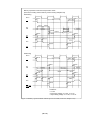
5.2 Operation Timing in Memory Expansion and Microprocessor Modes (5V)
(1) Separate Bus, No-Wait
Table 5.2 and Figure 5.1 show the bus timing in the memory expansion mode and the microprocessor
mode (separate bus, no-wait).
Table 5.2 Memory expansion mode and microprocessor mode (separate bus, no-wait)
Symbol
Item
Actual MCU This product
[ns]
[ns]
Min.
Max.
Min.
Td (BCLK-AD)
Address output delay time
Th (BCLK-AD)
Address output hold time (BCLK standard)
4
See left
Th (RD-AD)
Address output hold time (RD standard)
0
See left
Th (WR-AD)
Address output hold time (WR standard)
0
See left
Td (BCLK-CS)
Chip-select output delay time
Th (BCLK-CS)
Chip-select output hold time (BCLK standard)
34
25
Td (BCLK-ALE) ALE signal output delay time
Th (BCLK-ALE) ALE signal output hold time
52
25
4
See left
25
-4
See left
See left
Td (BCLK-RD)
RD signal output delay time
Th (BCLK-RD)
RD signal output hold time
Td (BCLK-WR)
WR signal output delay time
Th (BCLK-WR)
WR signal output hold time
Td (BCLK-DB)
Data output delay time (BCLK standard)
Th (BCLK-DB)
Data output hold time (BCLK standard)
4
See left
Td (DB-WR)
Data output delay time (WR standard)
(*1)
(*2)
Th (WR-DB)
Data output hold time (WR standard)
0
See left
Td (DB-WR)=
109
f(BCLK)x2
0
109
f(BCLK)x2
0
( 47 / 72 )
32
See left
57
40
-40 [ns]
-42 [ns]
See left
25
*2 Calculated by the following formula according to the frequency of BCLK.
Td (DB-WR)=
32
25
*1 Calculated by the following formula according to the frequency of BCLK.
Max.
Memory expansion mode and microprocessor mode (no-wait)
Read timing
BCLK
CSi
ADi
BHE
ALE
RD
DB
Write timing
BCLK
CSi
ADi
BHE
ALE
WR, WRL,
WRH
DB
Conditions:
• VCC=5V
• Input timing voltage: VIL=0.8V, VIH=2.5V
• Output timing voltage: VOL=0.8V, VOH=2.0V
Figure 5.1 Memory expansion mode and microprocessor mode (no-wait)
( 48 / 72 )
(2) Separate Bus, With Wait, Accessing External Memory Area
Table 5.3 and Figure 5.2 show the bus timing in the memory expansion mode and the microprocessor
mode (with wait, accessing external memory area).
Table 5.3 Memory expansion mode and microprocessor mode (with wait, external memory area)
Symbol
Item
Actual MCU This product
[ns]
[ns]
Min.
Max.
Min.
Td (BCLK-AD)
Address output delay time
Th (BCLK-AD)
Address output hold time (BCLK standard)
4
See left
Th (RD-AD)
Address output hold time (RD standard)
0
See left
Th (WR-AD)
Address output hold time (WR standard)
0
See left
Td (BCLK-CS)
Chip-select output delay time
Th (BCLK-CS)
Chip-select output hold time (BCLK standard)
34
25
Td (BCLK-ALE) ALE signal output delay time
Th (BCLK-ALE) ALE signal output hold time
52
25
4
See left
25
-4
See left
See left
Td (BCLK-RD)
RD signal output delay time
Th (BCLK-RD)
RD signal output hold time
Td (BCLK-WR)
WR signal output delay time
Th (BCLK-WR)
WR signal output hold time
Td (BCLK-DB)
Data output delay time (BCLK standard)
Th (BCLK-DB)
Data output hold time (BCLK standard)
4
See left
Td (DB-WR)
Data output delay time (WR standard)
(*1)
(*2)
Th (WR-DB)
Data output hold time (WR standard)
0
See left
Td (DB-WR)=
109
f(BCLK)
0
109
f(BCLK)
0
( 49 / 72 )
32
See left
57
40
-40 [ns]
-42 [ns]
See left
25
*2 Calculated by the following formula according to the frequency of BCLK.
Td (DB-WR)=
32
25
*1 Calculated by the following formula according to the frequency of BCLK.
Max.
Memory expansion mode and microprocessor mode
(with wait, accessing external memory area)
Read timing
BCLK
CSi
ADi
BHE
ALE
RD
DB
Write timing
BCLK
CSi
ADi
BHE
ALE
WR, WRL,
WRH
DBi
Conditions:
• VCC=5V
• Input timing voltage: VIL=0.8V, VIH=2.5V
• Output timing voltage: VOL=0.8V, VOH=2.0V
Figure 5.2 Memory expansion mode and microprocessor mode (with wait)
( 50 / 72 )
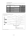
(3) Multiplex Bus, With Wait, Accessing External Memory Area
Table 5.4 and Figure 5.3 show the bus timing in the memory expansion mode and the microprocessor
mode (with wait, accessing external memory area and using multiplex bus).
Table 5.4 Memory expansion mode and microprocessor mode (with wait, multiplex bus)
Symbol
Actual MCU This product
[ns]
[ns]
Item
Min.
Td (BCLK-AD)
Address output delay time
Th (BCLK-AD)
Address output hold time (BCLK standard)
Th (RD-AD)
Max.
Min.
52
25
4
See left
Address output hold time (RD standard)
(*1)
(*2)
Th (WR-AD)
Address output hold time (WR standard)
(*1)
(*2)
Td (BCLK-CS)
Chip-select output delay time
Th (BCLK-CS)
Chip-select output hold time (BCLK standard)
Th (RD-CS)
34
25
4
See left
Chip-select output hold time (RD standard)
(*1)
See left
Th (WR-CS)
Chip-select output hold time (WR standard)
(*1)
See left
Td (BCLK-RD)
RD signal output delay time
Th (BCLK-RD)
RD signal output hold time
Td (BCLK-WR)
WR signal output delay time
Th (BCLK-WR)
WR signal output hold time
Td (BCLK-DB)
Data output delay time (BCLK standard)
Th (BCLK-DB)
Data output hold time (BCLK standard)
4
See left
Td (DB-WR)
Data output delay time (WR standard)
(*1)
See left
Th (WR-DB)
Data output hold time (WR standard)
(*1)
See left
35
25
0
See left
37
25
0
Th (BCLK-ALE) ALE output hold time (BCLK standard)
See left
40
Td (BCLK-ALE) ALE output delay time (BCLK standard)
See left
25
See left
-4
See left
ALE output delay time (Address standard)
(*1)
See left
Th (ALE-AD)
ALE output hold time (Address standard)
30
See left
Td (AD-RD)
After address RD signal output delay time
0
See left
Td (AD-WR)
After address WR signal output delay time
0
See left
Tdz (RD-AD)
Address output floating start time
8
See left
*2 Calculated by the following formulas according to the frequency of BCLK.
f(BCLK)x2
○
○
Th (RD-AD)=
○
109
[ns]
○
f(BCLK)x2
[ns]
Th (WR-AD)=
109
f(BCLK)x2
109
f(BCLK)x2
-14 [ns]
-14 [ns]
f(BCLK)x2
○
○
[ns]
f(BCLK)x2
○
○
○
○
○
[ns]
○
f(BCLK)x2
109
○
109
-40 [ns]
-25 [ns]
○
Td (AD-ALE)=
f(BCLK)x2
○
Th (WR-DB)=
109x3
○
Td (DB-WR)=
Th (RD-CS)=
○
109
○
f(BCLK)x2
[ns]
○
Th (WR-CS)=
109
○
Th (RD-CS)=
○
○
Th (WR-AD)=
109
○
Th (RD-AD)=
○
○
○
○
○
Td (AD-ALE)
*1 Calculated by the following formulas according to the frequency of BCLK.
( 51 / 72 )
Max.
Th (WR-CS)=
109
f(BCLK)x2
109
f(BCLK)x2
-12 [ns]
-12 [ns]
Memory expansion mode and microprocessor mode
(with wait, accessing external memory area and using multiplex bus)
Read timing
BCLK
CSi
ADi
DBi
ADi
BHI
ALE
RD
Write timing
BCLK
CSi
ADi
DBi
ADi
BHI
ALE
WR, WRL,
WRH
Conditions:
• VCC=5V
• Input timing voltage: VIL=0.8V, VIH=2.5V
• Output timing voltage: VOL=0.8V, VOH=2.0V
Figure 5.3 Memory expansion mode and microprocessor mode (with wait, multiplex bus)
( 52 / 72 )
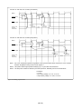
(4) Timing Requirements
Table 5.5, Figures 5.4 and 5.5 show timing requirements in the memory expansion mode and the
microprocessor mode.
Table 5.5 Timing requirements (VCC=5V)
Symbol
Actual MCU This product
[ns]
[ns]
Item
Min.
Tsu (DB-RD)
Data input setup time
Max.
Min.
40
See left
Tsu (RDY-BCLK) RDY* input setup time
30
50
Tsu (HOLD-BCLK) HOLD* input setup time
40
(*1)
Th (RD-DB)
0
See left
Th (BCLK-RDY) RDY* input hold time
0
See left
Th (BCLK-HOLD) HOLD* input hold time
0
See left
Data input hold time
Td (BCLK-HLDA) HLDA* output delay time
40
Max.
See left
*1 Minimum 13ns (The definition is different from that of the actual MCU. For details, see Figure 5.5.)
Memory expansion mode and microprocessor mode
(only for "with wait")
BCLK
RD
(separate bus)
WR, WRL, WRH
(separate bus)
RD
(multiplex bus)
WR, WRL, WRH
(multiplex bus)
RDY input
Conditions:
• VCC=5V
• Input timing voltage: VIL=1.0V, VIH=4.0V
• Output timing voltage: VOL=2.5V, VOH=2.5V
Figure 5.4 Timing requirements
( 53 / 72 )
Common to "with wait" and "no-wait" (actual MCU)
BCLK
HOLD input
HLDA output
P0, P1, P2,
P3, P4,
P50 to P52
Common to "with wait" and "no-wait" (this product)
BCLK
HOLD input
HLDA output
P0, P1, P2,
P3, P4,
P50 to P52
Note 1. P00 to P52 will be high-impedance regardless of the input level of BYTE pin and ports P40 to P43 function
selection bit (PM06) of the processor mode register 0.
Note 2. This product will be high-impedance delaying by 2.5 cycles than the actual MCU.
Note 3. The setup time of HOLD is defined by the startup of BCLK, differently from that of actual MCUs.
Conditions:
• VCC=5V
• Input timing voltage: VIL=1.0V, VIH=4.0V
• Output timing voltage: VOL=2.5V, VOH=2.5V
Figure 5.5 Timing requirements
( 54 / 72 )
5.3 Electrical Characteristics
Tables 5.6 and 5.7 list IC electrical characteristics of the user interface.
Table 5.6 Electrical characteristics of 74HC4066AFT (P100 to P107, AN0 to AN7)
Symbol
Standard values
Parameter
VCC
Min.
3.15
Standard
VIHC
High level control input voltage
4.5
VILC
Low level control input voltage
4.5
RON
ON resistance
4.5
96
RON
Difference of ON resistances
4.5
10
Max.
Unit
V
1.35
V
200
Ω
Ω
Table 5.7 Electrical characteristics of M60074-0111FP (P00 to P57)
Symbol
Standard values
Parameter
Condition
VIL
Min.
Standard
Max.
VCC=4.5V
0
1.35
VCC=5.5V
3.85
5.5
VCC=5.0V
|IO|<1µA
4.95
V
VCC=4.5V
VOL=0.4V
8
mA
V
Input voltage
VIH
VOH
VOL
Output voltage
IOL
Output current
IOH
VCC=4.5V
VOH=4.1V
IIL
VCC=5.5V
VI=0V
IIH
IOZL
Input leak current
OFF state output leak current
IOZH
CIO
Unit
( 55 / 72 )
V
-8
mA
-1
+1
µA
VCC=5.5V
VI=5.5V
-1
+1
µA
VCC=5.5V
VO=0V
-1
+1
µA
VCC=5.5V
VO=5.5V
-1
+1
µA
15
pF
f=1MHz
VCC=0V
I/O pin capacity
0.05
7
5.4 Connection Diagram
Figures 5.6 and 5.7 show the connection diagram of M306V2T-RPD-E. This connection diagram
mainly shows the interface section, and the circuits which are not connected to the target system such
as the emulator's control system are omitted.
∗ : Control signal
Figure 5.6 Connection diagram 1
( 56 / 72 )
∗ : Control signal
Figure 5.7 Connection diagram 2
( 57 / 72 )
5.5 External Dimensions
(1) External Dimensions of Emulation Pod
Unit: mm
Figure 5.8 External dimensions of emulation pod
( 58 / 72 )
(2) External Dimensions of Pitch Converter Board (FLX-100LCC)
Figure 5.9 shows the external dimensions of the pitch converter board FLX-100LCC for 100-pin
LQFP (100D0).
Unit: mm
Figure 5.9 External dimensions of pitch converter board (FLX-100LCC)
( 59 / 72 )
MEMO
( 60 / 72 )
Chapter 6. Troubleshooting
This chapter describes how to troubleshoot when this product does not work properly.
6.1 Flowchart to Remedy the Troubles ............................................................................................ 62
6.2 When the Emulator Debugger Does Not Start Up Properly....................................................... 63
(1) When the LED Display of PC4701 is Abnormal .................................................................. 63
(2) Errors Occur When the Emulator Debugger Starts Up
(When the target system is connected) ...................................................................... 64
(3) Errors Occur When the Emulator Debugger Starts Up
(When the target system is not connected) ................................................................ 65
6.3 Operation Differs from That of Actual MCUs ........................................................................... 65
(1) A-D Conversion Values are Different from Expected Values .................................................. 65
( 61 / 72 )
Chapter 6. Troubleshooting
6.1 Flowchart to Remedy the Troubles
Figure 6.1 shows the flowchart to remedy the troubles from when power to the emulator is activated
until the emulator debugger starts up. Check this while the target system is disconnected.
Turning on the power of PC4701
LED status of
PC4701 front panel
LED status not normal
1. Check emulator system connections.
See, "3.6 Connecting the PC4701 and Emulation Pod"
(page 36).
2. Redownload the firmware.
See "4.2 Downloading Firmware" (page 42).
3. Restart the PC4701 system.
Init dialog box of emulator
debugger displayed
Display not normal.
Error displayed.
1. Check the environmental setting etc. of the emulator debugger.
See the user's manual of the emulator debugger.
2. Reinstall the emulator debugger.
Program window of emulator debugger displayed
Figure 6.1 Flowchart to remedy the troubles
( 62 / 72 )
6.2 When the Emulator Debugger Does Not Start Up Properly
(1) When the LED Display of PC4701 is Abnormal
Table 6.1 LED's abnormal display and its checkpoints
Error
LEDs do not light up.
Connection to
the target system
Checkpoint
-
Recheck the power cable is connected to the
PC4701.
See the instruction manual of the PC4701.
All LEDs remain lit.
The "POWER" LED of
"STATUS OF TARGET"
does not light up.
-
Connected
Recheck the connection between the PC4701 and
this product.
See "3.6 Connecting the PC4701 and Emulation
Pod" (page 36).
Check power is properly supplied to the target
system and that the target system is properly
grounded.
(1) Check both the main and sub clocks of the
emulator debugger are not set to "EXT".
Disconnected
See the CLK command of the emulator
debugger.
(2) Check the oscillation circuit in the emulation
pod is oscillating.
The "CLOCK" LED of
"STATUS OF TARGET"
does not light up.
See "3.3 Selecting Clock Supply" (page 29).
Connected
(1) Check the oscillation circuit in the target system
is oscillating.
(2) Check the switches in the emulation pod are
correctly set.
See "3.2 Switch Settings" (page 25).
( 63 / 72 )
(2) Errors Occur When the Emulator Debugger Starts Up
(When the target system is connected)
Table 6.2 Checkpoints of errors when starting up the emulator debugger (target is connected)
Error
Checkpoint
Check all emulator debugger settings, interface cable
connection and switches on the rear of the PC4701 match.
Communication error occurred
Data was not sent to the target
See the instruction manuals of the PC4701 and the
emulator debugger.
(1) Download the proper firmware.
See "4.2 Downloading Firmware" (page 42).
Target system cannot be properly built
(2) Recheck the connection between the PC4701 and
this product.
See "3.6 Connecting the PC4701 and Emulation
Pod" (page 36).
M3T-PD30 version is not the same version Download the proper firmware.
as the firmware in the target
See "4.2 Downloading Firmware" (page 42).
Target MCU is in the reset state
Check the reset pin of the target system has changed
from "Low" to "High" level.
Target MCU cannot be reset
(1) If the reset circuit of the target system has a watchdog
timer, disable the timer.
(2) Check power is properly supplied to the target system
and that the target system is properly grounded.
(3) The program may be uncontrollable in areas where
memory not allocated. Recheck the map setting.
(1) The MCU is either in the stop mode or wait mode.
Either reset the MCU or cancel the mode with an
interrupt.
Target is in HOLD state
See the MCU specifications.
(2) The program may be uncontrollable in areas where
memory not allocated. Recheck the map setting.
(1) Check the oscillation circuit of the target system is
oscillating properly.
(2) Check the switches in the emulation pod are correctly
set.
Target clock is stopped
See "3.2 Switch Settings" (page 25).
Target MCU is not receiving power
( 64 / 72 )
Check power is properly supplied to the target system
and that the target system is properly grounded.
(3) Errors Occur When the Emulator Debugger Starts Up
(When the target system is not connected)
Table 6.3 Checkpoints of errors when starting up the emulator debugger (target is not connected)
Error
Checkpoint
Check all emulator debugger settings, interface cable
connection and switches on the rear of the PC4701 match.
Communication error occurred
Data was not sent to the target
See the instruction manuals of the PC4701 and the
emulator debugger.
(1) Download the proper firmware.
See "4.2 Downloading Firmware" (page 42).
Target system cannot be properly built
(2) Recheck the connection between the PC4701 and
this product.
See "3.6 Connecting the PC4701 and Emulation Pod"
(page 36).
M3T-PD30 version is not the same version Download the proper firmware.
as the firmware in the target
See "4.2 Downloading Firmware" (page 42).
The program may be uncontrollable in areas where
memory not allocated. Recheck the map setting.
Target MCU cannot be reset
(1) The MCU is either in the stop mode or wait mode.
Either reset the MCU or cancel the mode with an
interrupt.
Target is in HOLD state
See the MCU specifications.
(2) The program may be uncontrollable in areas where
memory not allocated. Recheck the map setting.
Check the switches in the emulation pod are correctly set.
Target clock is stopped
See "3.2 Switch Settings" (page 25).
6.3 Operation Differs from That of Actual MCUs
(1) A-D Conversion Values are Different from Expected Values
As a flexible cable, a pitch converter board and other devices are used between the evaluation MCU
and the target system, the A-D converter operates differently from the actual MCU. Make the final
evaluation of the A-D converter from the actual MCU.
( 65 / 72 )
MEMO
( 66 / 72 )
Chapter 7. Maintenance and Guarantee
This chapter describes how to maintenance, repair provisions and how to request for repair.
7.1 Maintenance ............................................................................................................................... 68
7.2 Guarantee .................................................................................................................................... 68
7.3 Repair Provisions........................................................................................................................ 68
7.4 How to Request for Repair ......................................................................................................... 69
( 67 / 72 )
Chapter 7. Maintenance and Guarantee
7.1 Maintenance
If dust or dirt collects on any equipment of your emulation system, wipe it off with a dry soft cloth.
Do not use thinner or other solvents because these chemicals can cause the equipment's surface
coating to separate.
7.2 Guarantee
If your product becomes faulty within twelve months after its purchase while being used under good
conditions by observing "Precautions for Safety" described in Chapter 1 of this user's manual, we will
repair or replace your faulty product free of charge. Note, however, that if your product's fault is raised
by any one of the following causes, we will repair it or replace it with new one with extra-charge:
• Misuse, abuse, or use under extraordinary conditions
• Unauthorized repair, remodeling, maintenance, and so on
• Inadequate user's system or misuse of it
• Fires, earthquakes, and other unexpected disasters
In the above cases, contact your local distributor. If your product is being leased, consult the leasing
company or the owner.
7.3 Repair Provisions
(1) Repair with extra-charge
The products elapsed more than twelve months after purchase can be repaired with extra-charge.
(2) Replacement with extra-charge
If your product's fault falls in any of the following categories, the fault will be corrected by
replacing the entire product instead of repair, or you will be advised to purchase new one,
depending on the severity of the fault.
• Faulty or broken mechanical portions
• Flaw, separation, or rust in coated or plated portions
• Flaw or cracks in plastic portions
• Faults or breakage caused by improper use or unauthorized repair or modification
• Heavily damaged electric circuits due to overvoltage, overcurrent or shorting of power supply
• Cracks in the printed circuit board or burnt-down patterns
• Wide range of faults that makes replacement less expensive than repair
• Unlocatable or unidentified faults
(3) Expiration of the repair period
When a period of twelve months elapses after the model was dropped from production, repairing
products of the model may become impossible.
(4) Transportation fees at sending your product for repair
Please send your product to us for repair at your expense.
( 68 / 72 )
7.4 How to Request for Repair
If your product is found faulty, follow the procedure below to send your product for repair.
Customer
Fill in the Repair Request Sheet included with this product, then send it
along with this product for repair to your local distributor. Make sure
that information in the Repair Request Sheet is written in as much detail
as possible to facilitate repair.
Distributor
After checking the contents of fault, the distributor should please send
the faulty product along with the Repair Request Sheet to Renesas
Solutions Corp.
Renesas Solutions
When the faulty product is repaired, it will be returned to the customer
at the earliest convenience.
CAUTION
Note on Transporting the Product:
• When sending your product for repair, use the packing box and cushion material supplied with this
product when delivered to you and specify handling caution for it to be handled as precision
equipment. If packing of your product is not complete, it may be damaged during transportation.
When you pack your product in a bag, make sure to use conductive polyvinyl supplied with this
product (usually a blue bag). When you use other bags, they may cause a trouble on your product
because of static electricity.
( 69 / 72 )
MEMO
( 70 / 72 )
M306V2T-RPD-E User's Manual
Rev.1.00
September 1, 2003
REJ10J0266-0100Z
COPYRIGHT ©2003 RENESAS TECHNOLOGY CORPORATION
AND RENESAS SOLUTIONS CORPORATION ALL RIGHTS RESERVED